EP0320015A2 - Appareil de transmission de données par induction - Google Patents
Appareil de transmission de données par induction Download PDFInfo
- Publication number
- EP0320015A2 EP0320015A2 EP88120656A EP88120656A EP0320015A2 EP 0320015 A2 EP0320015 A2 EP 0320015A2 EP 88120656 A EP88120656 A EP 88120656A EP 88120656 A EP88120656 A EP 88120656A EP 0320015 A2 EP0320015 A2 EP 0320015A2
- Authority
- EP
- European Patent Office
- Prior art keywords
- signal
- data
- transmission
- resonance circuit
- oscillator
- Prior art date
- Legal status (The legal status is an assumption and is not a legal conclusion. Google has not performed a legal analysis and makes no representation as to the accuracy of the status listed.)
- Granted
Links
- 230000001939 inductive effect Effects 0.000 title 1
- 230000005540 biological transmission Effects 0.000 claims abstract description 211
- 230000010355 oscillation Effects 0.000 claims abstract description 77
- 239000003990 capacitor Substances 0.000 claims description 33
- 238000001514 detection method Methods 0.000 claims description 7
- 230000005674 electromagnetic induction Effects 0.000 claims description 5
- 238000007493 shaping process Methods 0.000 claims description 2
- 230000008878 coupling Effects 0.000 abstract description 5
- 238000010168 coupling process Methods 0.000 abstract description 5
- 238000005859 coupling reaction Methods 0.000 abstract description 5
- 238000010586 diagram Methods 0.000 description 24
- 238000004891 communication Methods 0.000 description 9
- 230000007423 decrease Effects 0.000 description 6
- 230000003111 delayed effect Effects 0.000 description 6
- 238000005070 sampling Methods 0.000 description 6
- 238000010276 construction Methods 0.000 description 4
- 230000004044 response Effects 0.000 description 4
- 238000013459 approach Methods 0.000 description 3
- 230000004048 modification Effects 0.000 description 3
- 238000012986 modification Methods 0.000 description 3
- 230000002238 attenuated effect Effects 0.000 description 2
- 230000010354 integration Effects 0.000 description 2
- 230000008859 change Effects 0.000 description 1
- 230000005672 electromagnetic field Effects 0.000 description 1
- 230000006870 function Effects 0.000 description 1
- 238000009499 grossing Methods 0.000 description 1
- 230000006698 induction Effects 0.000 description 1
- 230000007257 malfunction Effects 0.000 description 1
- 238000000034 method Methods 0.000 description 1
- 230000002093 peripheral effect Effects 0.000 description 1
- 230000008054 signal transmission Effects 0.000 description 1
Images


Classifications
-
- G—PHYSICS
- G06—COMPUTING; CALCULATING OR COUNTING
- G06K—GRAPHICAL DATA READING; PRESENTATION OF DATA; RECORD CARRIERS; HANDLING RECORD CARRIERS
- G06K19/00—Record carriers for use with machines and with at least a part designed to carry digital markings
- G06K19/06—Record carriers for use with machines and with at least a part designed to carry digital markings characterised by the kind of the digital marking, e.g. shape, nature, code
- G06K19/067—Record carriers with conductive marks, printed circuits or semiconductor circuit elements, e.g. credit or identity cards also with resonating or responding marks without active components
- G06K19/07—Record carriers with conductive marks, printed circuits or semiconductor circuit elements, e.g. credit or identity cards also with resonating or responding marks without active components with integrated circuit chips
- G06K19/0723—Record carriers with conductive marks, printed circuits or semiconductor circuit elements, e.g. credit or identity cards also with resonating or responding marks without active components with integrated circuit chips the record carrier comprising an arrangement for non-contact communication, e.g. wireless communication circuits on transponder cards, non-contact smart cards or RFIDs
-
- G—PHYSICS
- G06—COMPUTING; CALCULATING OR COUNTING
- G06K—GRAPHICAL DATA READING; PRESENTATION OF DATA; RECORD CARRIERS; HANDLING RECORD CARRIERS
- G06K7/00—Methods or arrangements for sensing record carriers, e.g. for reading patterns
- G06K7/0008—General problems related to the reading of electronic memory record carriers, independent of its reading method, e.g. power transfer
-
- H—ELECTRICITY
- H04—ELECTRIC COMMUNICATION TECHNIQUE
- H04B—TRANSMISSION
- H04B5/00—Near-field transmission systems, e.g. inductive loop type
-
- H04B5/22—
-
- H04B5/263—
-
- H04B5/266—
-
- H04B5/77—
Definitions
- the present invention relates to a data communicating apparatus for communicating data between first and second devices which are contactlessly closely arranged or approached to each other by using an induction electromagnetic field and to an oscillator which is used in the communicating apparatus and transmits data by intermittently performing the oscillation.
- JP-A-62-63050 there has been proposed a data transmitting apparatus in which a data storing device to store tool data is provided for a tool shank or the like of a machine tool, the data is serially transmitted and written from a data input/output apparatus into the data storing device, or the content written is read out.
- the data communication between the data input/output apparatus and the data storing device is performed by using predetermined high frequency signals by frequency shift keying (FSK) modulating those high frequency signals.
- FSK frequency shift keying
- each of the data storing device and data input/output apparatus needs a PLL circuit or the like to demodulate the FSK signal, so that a large electric power consumption is required.
- an AC voltage induced from the data input/output (I/O) apparatus is rectified and the data storing device uses the resultant rectified voltage as a power source.
- the electric power consumption is large, the data communication cannot be performed unless the induced voltage is high, so that there is a drawback such that a distance at which the data communication can be performed is short.
- the data storing device has a battery, there is a drawback such that the life of the battery is short.
- the applicant of the present invention has already proposed a system (not published yet) in which in order to reduce the electric power consumption of the data storing device, when data is transmitted from the data storing device to the data I/O apparatus, a resonance frequency of a resonance circuit is discontinuously changed on the basis of the transmission data.
- a resonance frequency of a resonance circuit is discontinuously changed on the basis of the transmission data.
- a Colpits oscillator which is an LC type oscillator to transmit a signal by the electromagnetic induction and transmits a signal by intermittently performing the oscillation.
- a collector of a transistor Tr1 is connected to one end of an LC resonance circuit 51 consisting of a coil L1 and capacitors C21 and C22.
- a feedback resistor R21 is connected between a middle point of the coils C21 and C22 and an emitter of the transistor Tr1.
- the emitter of the transistor Tr1 is connected to the ground through an emitter resistor R22.
- a predetermined DC voltage is applied to one end of the resonance circuit 51.
- a middle point of resistors R23 and R24 to divide the power source voltage is connected to the base of the transistor Tr1.
- a predetermined voltage is applied as a bias to the base of the Tr1 and the base is connected to the ground by a capacitor C23 in an AC manner.
- An FET 52 for switching is provided to intermittently apply and shut off the terminal voltage of the base of the Tr1.
- the FET 52 is intermittently turned on/off in accordance with an input signal and the base of the oscillating transistor Tr1 is connected to the ground or a predetermined bias voltage is applied thereto.
- the oscillation can be intermittently performed in correspondence to the input voltage which is applied to the FET 52.
- the present invention is made in consideration of the foregoing problems in the conventional data transmitting apparatus and it is a technical subject of the invention to enlarge a communication distance by mutually transmitting a transmission signal by using a carrier of a predetermined frequency and by improving a transmission/reception efficiency.
- Another object of the invention is to make the oscillator of the second device unnecessary.
- Still another object of the invention is to improve the S/N ratio upon data transmission.
- Still another object of the invention is to provide an apparatus which can perform the full-duplex data communication by using a carrier of a predetermined frequency.
- the invention is made in consideration of the foregoing problems of the conventional oscillator and it is a technical subject of the invention to enable the oscillation to be started and stopped in an extremely short time in response to an input signal.
- a data communicating apparatus for performing a half-duplex data transmission of serial data between a first device and a second device.
- the first device comprises: an oscillator which has a first coil arranged on a surface which can face the second device; transmission pulse generating means for generating transmission pulse signals of a predetermined period having a first or second duty ratio in correspondence to a transmission data signal upon data transmission and a predetermined third duty ratio upon data reception, and for giving the transmission pulse signal of the predetermined period to the oscillator to cause the oscillator to intermittently perform the oscillation; a first resonance circuit which has a resonance frequency that is substantially equal to an oscillating frequency of the oscillator and which include a second coil arranged on the surface that can face the second device; reception gate signal generating means for receiving a signal corresponding to a transmission pulse of the transmission pulse generating means and for generating a reception gate signal having a timing when the oscillation of the oscillator is stopped; a detecting circuit for detecting an electromagnetic induction signal
- the second device comprises: a second resonance circuit which has a resonance frequency that is substantially equal to the oscillating frequency of the oscillator of the first device and which includes a third coil arranged on the surface that can face the first device ; a detecting circuit to detect a signal obtained in the second resonance circuit; a second comparator for reproducing the transmission pulse signal by discriminating a detection output of the detecting circuit by a predetermined threshold level; data demodulating means for demodulating the transmission data signal by the transmission pulse signals of the first and second duty ratios on the basis of an output of the second comparator upon data reception from the first device; and reverberation control means which has switching elements connected between the second resonance circuit and the ground and controls a reverberation that is caused in the second resonance circuit by turning on/off the switching elements in correspondence to the transmission data at the timing for the stop of the oscillation of the oscillator on the basis of the transmission pulse signal of the third duty ratio which is derived from the second comparator upon data transmission to the first device.
- the oscillation of the oscillator is intermittently performed at a predetermined period and the duty ratio is changed upon transmission, thereby allowing the binary signal to be transmitted to the second device.
- the transmission pulse signal is demodulated. Further, the original transmission data signal is demodulated on the basis of the duty ratio of that signal.
- the oscillation of the oscillator is intermittently performed by the predetermined third duty ratio and the switching elements which are provided for the resonance circuit of the second device are intermittently turned on/off in response to the transmission data signal at the stop of the oscillation, thereby controlling the reverberation obtained in the resonance circuit of the first device.
- the first device generates the reception gate signal of the stop period of the oscillation on the basis of the transmission pulse signal which is given to the oscillator and fetches only the reverberation by the reception gate signal, thereby detecting the reverberation.
- the signal is sampled at a predetermined timing of the reception gate signal and given to the first comparator and discriminated on the basis of the predetermined threshold level, thereby demodulating the transmission signal which is derived from the second device.
- the half-duplex data transmission of serial data is executed between the first and second devices by using the electromagnetic coupling. Since the data demodulating means of the second device demodulates the signal on the basis of the pulse width, there is no need to use a PLL circuit or the like and the circuit arrangement is relatively simple and the electric power consumption is small. Therefore, when the electric power for the second device is obtained from the first device, the transmission distance can be set to a long distance because of the small electric power consumption.
- the second device in the data communicating apparatus further has; a clock discriminating circuit for discriminating an oscillation signal obtained in the second resonance circuit on the basis of a comparison signal of the second comparator and for shaping the discriminated oscillation signal; and above data demodulating means for demodulating the transmission data signal by the transmission pulse signals of the first and second duty ratios on the basis of an output of the second comparator and a clock signal of the clock discriminating circuit upon reception of the data from the first device.
- the clock discriminating circuit in the clock discriminating circuit, the oscillation signal of the oscillator obtained from the first device is shaped to form a clock, the duty ratio is discriminated on the basis of the clock signal, and thereby demodulating the original transmission data signal. Therefore, a clock generator is unnecessary in the second device and the circuit construction is simplified.
- the first device in the data communicating apparatus further has: resonance control means which is connected in parallel with the first resonance circuit and which has a series connection circuit comprising of a resistor and an analog switch that is turned on/off by the reception gate signal and which controls Q of the first resonance circuit.
- the oscillator of the first device When data is transmitted from the second device to the first device, the oscillator of the first device is intermittently driven. When the oscillator is driven, Q of the first resonance circuit is reduced on the basis of an output of the reception gate signal generator and only when the reverberation is received, Q is raised, so that only the reverberation can be accurately detected in the second resonance circuit. Therefore, data can be transmitted from the second device to the first device at a high S/N ratio.
- a data communicating apparatus for performing a data transmission of serial data between a first device and a second device.
- the first device comprises: an oscillator which has a first coil arranged on a surface that can face the second device; transmission pulse generating means for continuously generating a transmission pulse signal of a first or second duty ratio, for switching the first and second duty ratios in correspondence to the transmission data signal upon data transmission, for giving the transmission pulse signal to the oscillator, and thereby for intermittently performing the oscillation of the oscillator; a first resonance circuit which has a resonance frequency that is substantially equal to an oscillating frequency of the oscillator and includes a second coil arranged on the surface that can face the second device; reception gate signal generating means for receiving a signal corresponding to a transmission pulse of the transmission pulse generating means and for generating a reception gate signal having a timing at the stop of the oscillation of the oscillator; a detecting circuit to detect an electromagnetic induction signal obtained in the first resonance circuit for a time when the reception gate signal is
- the second device comprises: a second resonance circuit which has a resonance frequency that is substantially equal to an oscillating frequency of the oscillator of the first device and includes a third coil arranged on the surface that can face the first device; a detecting circuit to detect a signal obtained in the second resonance circuit; a second comparator to reproduce the transmission pulse signal by discriminating the detection output on the basis of a predetermined threshold level; data demodulating means for demodulating the transmission data signal by the transmission pulse signals having the first and second duty ratios on the basis of an output of the second comparator upon reception of the data from the first device; and reverberation control means which has switching elements connected between the second resonance circuit and the ground and controls a reverberation caused in the second resonance circuit by turning on/off the switching elements in correspondence to the transmission data at the timing for the stop of the oscillation of the oscillator on the basis of the transmission pulse signal derived from the second comparator upon data transmission to the first device.
- the first device always generates a transmission pulse of the first or second duty ratio on the basis of the transmission data.
- the duty ratio is changed by the transmission data and the oscillation of the oscillator is intermittently performed and the data is transmitted to the second device.
- the second device detects the transmitted signal and discriminates by the predetermined threshold level, thereby demodulating the transmission pulse signal. Further, the original transmission data signal is demodulated on the basis of the duty ratio of the signal.
- the oscillation of the oscillator is intermittently performed on the basis of the transmission pulse signal of the first or second duty ratio of an arbitrary data series.
- the switching elements which are provided for the resonance circuit of the second device are turned on or off in accordance with the transmission data signal, thereby controlling the reverberation derived in the resonance circuit of the first device.
- the first device generates a reception gate signal for the period of time when the oscillation of the oscillator stops and takes out only the reverberation by the reception gate signal and detectes the reverberation.
- the detected signal is sampled at a predetermined timing of the reception gate signal and given to the first comparator and discriminated on the basis of the predetermined threshold level, thereby demodulating the transmission signal transmitted from the second device.
- the data transmission can be performed between the first and second devices by using the electromagnetic coupling.
- the data transmission is executed by transmitting an arbitrary signal from the first device, so that the full-duplex data transmission can be executed by changing the transmission signal of the first device by the transmission data. Therefore, by sequentially transmitting the data which were mutually transmitted from the other device, the transmission content can be checked every bit.
- an oscillator which is used in a data communicating apparatus to transmit a signal by the intermittent oscillation and comprises: a parallel resonance circuit comprising of resonance elements including a coil and a capacitor; and a transistor whose collector is connected to one end of the parallel resonance circuit and which is fed back to a base from a middle point provided for the resonance elements of the resonance circuit, wherein the oscillator has a switching element which is connected between the coil and the capacitor of the resonance circuit and opens or closes the resonance circuit, and the oscillation is intermittently executed by the switching element.
- the switching element is serially connected to the resonance circuit and the intermittent oscillation is controlled by the switching element. Since a current is directly supplied to the resonance circuit from a power source by closing the switching element, the leading edge can be made sharp. By opening the switching element, the charges in the capacitor of the resonance circuit are discharged through the transistor, so that the oscillation is stopped in an extremely short time.
- the leading time of the oscillation and the stop time of the oscillation can be extremely made fast. Therefore, if the invention is applied to the oscillator of the data communicating apparatus for transmitting a signal by the intermittent oscillation, there are advantages such that the data transmission can be performed at a high speed and the signal transmission can be accurately executed.
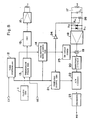
- Fig. 1 is a block diagram showing a whole arrangement of an article identifying system to which a data communicating apparatus according to an embodiment of the present invention is applied.
- the data communicating apparatus has a write/read control unit 1 as a first device and an ID unit 3 as a second device which is attached to an article 2 or the like.
- the write/read control unit 1 is fixedly provided and when an article is moved, the ID unit 3 attached to the article 1 approaches the write/read control unit 1.
- the write/read control unit 1 has first and second coils L1 and L2 at positions where the first and second coils can face the ID unit 3 when the ID unit 3 appraoches to the unit 1.
- the ID unit 3 has a third coil L3 at a position where the third coil can face the first and second coils.
- the write/read control unit 1 is further connected to an upper control unit 4. After the control unit 4 transmitted a transmission control signal CT to the write/read control unit 1, the control unit sends transmission data SD and reads reception data RD which is obtained from the write/read control unit 1.
- the write/read control unit 1 has a clock generator 11 to generate a predetermined clock signal, a time controller 12 to generate a timing signal on the basis of the clock signal, and a transmission pulse generator 13.
- the time controller 12 sends a transmission/reception switching signal to the transmission pulse generator 13 and a reception gate generator 14.
- the control unit 4 transmits the transmission data SD to the transmission pulse generator 13.
- the transmission pulse generator 13 When the transmission/reception switching signal from the time controller 12 indicates the transmission mode, the transmission pulse generator 13 counts the clocks generated from the clock generator 11 for a predetermined period of time and generates a transmission pulse signal having a first or second duty ratio (e.g., 30% or 70%) in accordance with the transmission data SD at a predetermined period of time T. An output of the transmission pulse generator 13 is input to an oscillator 15. When the transmission/reception switching signal indicates the reception mode, the generator 13 generates a transmission pulse signal of a third duty ratio (for instance, 50%). The oscillator 15 oscillates a signal of a predetermined frequency only when the transmission pulse signal is given from the transmission pulse generator 13. An oscillation output of the oscillator 15 is supplied to the first coil L1 for transmission through an amplifier 16.
- a first or second duty ratio e.g. 30% or 70%
- the write/read control unit 1 also has the second coil L2 for reception.
- a capacitor C1 is connected in parallel with the coil L2, thereby constructing a first resonance circuit 17 which resonates with the oscillating frequency of the oscillator 15.
- An induced voltage developed across the first resonance circuit 17 is applied to an amplifier 18.
- the amplifier 18 amplifies the induced voltage and gives an output to a detecting circuit 20 through an analog switch 19.
- the reception gate generator 14 When the transmission/reception switching signal generated from the time controller 12 indicates the reception mode, the reception gate generator 14 generates a reception gate signal which is delayed by a predetermined time corresponding to, e.g., one clock from the trailing edge of the transmission pulse.
- the reception gate signal is given as a gate signal to the analog switch 19.
- the clock signal of the clock generator 11 and reception gate signal of the reception gate generator 14 is also given to a sampling signal generator 21.
- the generator 21 gives a signal of a predetermined timing of the reception gate signal, for instance, a signal of one clock just before the trailing edge as a sampling signal to a sample and hold circuit 22.
- the detecting circuit 20 detects the signal obtained through the analog switch 19, thereby obtaining an integration signal or its envelope signal.
- the detection signal is input to the sample and hold circuit 22.
- the sample and hold circuit 22 holds the input signal on the basis of the sampling signal.
- An output of the sample and hold (S/H) circuit 22 is input to a first comparator 23.
- the comparator 23 obtains a binary signal by discriminating the signal held on the basis of a predetermined threshold level.
- An output of the comparator 23 is input as the reception signal RD to the upper control unit 4.
- the ID unit 3 has a second resonance circuit 30 consisting of a coil L3 and a capacitor C2 provided on the surface which faces the write/read control unit 1.
- An induced voltage across the second resonance circuit 30 is given to a detecting circuit 31.
- the detecting circuit 31 detects the input signal and its output is given to a second comparator 32.
- a predetermined threshold level is set in the comparator 32.
- the detection output is discriminated by the predetermined threshold level.
- An output of the comparator 32 is given to both of a counter 33 and a digital comparator 34.
- the counter 33 is reset by a leading edge of the output of the comparator 32.
- the counter 33 counts the clock signals from a clock generator 35 which are input when the output (transmission pulse) of the comparator 32 is held at the H level.
- a count value is given to the digital comparator 34.
- the digital comparator 34 compares the count value of the counter 33 with a predetermined value at the timing of the trailing edge of the output of the comparator 32, thereby obtaining the "L” or "H” level output depending on whether the count value exceeds the predetermined value or not.
- An output of the digital comparator 34 is input to a memory control unit 36.
- a memory 37 serving as memory means of the ID unit 3 is connected to the memory control unit 36. Signals which are transmitted from the write/read control unit 1 are data and command.
- the memory control unit 36 writes the given data into the memory 37 or reads out the data from the memory 37 on the basis of the command.
- An output of the memory control unit 36 is given to a reverberation control pulse generator 38.
- the reverberation control pulse generator 38 On the basis of the transmission data to be transmitted to the write/read control unit 1 which was read out of the memory 37 by the memory control unit 36 at the timing when the output of the comparator 32 is at the L level, the reverberation control pulse generator 38 generates a reverberation control pulse of a predetermined width when the transmission data is at the L level.
- FETs 39 and 40 as switching elements are connected through resistors between both ends of the resonance circuit 30 and the ground, respectively.
- the FETs 39 and 40 function to connect both ends of the resonance circuit 30 to the ground on the basis of the reverberation control pulse from the generator 38, respectively.
- the ID unit 3 has a battery 41 as shown in the diagram and a power source is supplied from the battery 41 to each section.
- the counter 33, digital comparator 34, and clock generator 35 construct data demodulating means for discriminating the transmission data SD on the basis of the output of the comparator 32 having the first or second duty ratio, that is, the transmission pulse signal which is given from the write/read control unit 1.
- the reverberation control pulse generator 38 and FETs 39 and 40 as the switching elements for connecting both ends of the resonance circuit 30 to the ground construct reverberation control means for controlling the reverberation of the resonance circuit 30.
- the transmission control signal CT is sent from the upper control unit 4 to the time controller 12.
- the time controller 12 gives the transmission/reception switching signal to the transmission pulse generator 13.
- the signal of the transmission data SD (for instance, "HLLH" as shown in the diagram) is sent from the upper control unit 4 to the transmission pulse generator 13.
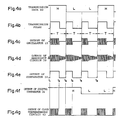
- the transmission pulse generator 13 generates the transmission pulse signal of the first or second duty ratio which corresponds to the H or L logic level of the transmission data and is different from each other at a predetermined period T from times t1, t3, t5 and t6.
- the oscillation of the oscillator 15 is intermittently performed by the transmission pulse signal as shown in Fig. 4c. Therefore, when the ID unit 3 approaches, as shown in Fig. 4d, a signal of a predetermined amplitude is obtained across the resonance circuit 30 for the driving time of the oscillator 15, that is, for the time intervals from t1 to t2, t3 to t4, etc. and the signal is attenuated after that.
- the signal is then detected by the detecting circuit 31 and compared by the comparator 32 on the basis of the predetermined threshold level. Therefore, the same signal as the transmission pulse signal as shown in Fig. 4e is obtained by the comparator 32.
- the signal is input to the counter 33 and digital comparator 34.
- a count value larger than a predetermined value is obtained in the counter 33 at the time point t2 when the output of the comparator 32 trails (the transmission pulse of the first duty ratio corresponding to the H level is obtained).
- a count value lower than the predetermined value is derived in the counter 33 at the time point t4 (the transmission pulse of the second duty ratio corresponding to the L level is obtained).
- the digital comparator 34 discriminates the count value at times t2 and t4 and outputs a signal indicative of the result of the discrimination to the memory control unit 36 at a timing which is delayed by one period T than the transmission data SD as shown in Fig. 4f.
- the data can be transmitted from the write/read control unit 1 to the ID unit 3.
- the signal of a predetermined frequency is merely intermittently supplied or shut off, by making the resonance frequency of the resonance circuit 30 coincide with the oscillating frequency of the oscillator 15, the high efficient data transmission can be performed.
- the voltage level induced in the ID unit 3 rises, so that the communication distance can be enlarged by the oscillation output.
- the transmission/reception switching signal of the time controller 12 of the write/read control unit 1 is switched to the reception mode.
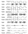
- the transmission pulse generator 13 generates the transmission pulse signal of a predetermined period T having a predetermined third duty ratio of, e.g., 50% as shown in Fig. 5a.
- the comparator 32 outputs a read clock signal of the duty ratio of 50% as shown in Fig. 5c.
- the data signal is read out of the memory 37 by the memory control unit 36.
- FIG. 5d shows an example of the signal in the case where the data read out by the memory control unit 36 is "HLHL".
- the data signal is input to the reverberation control pulse generator 38. Only when the logic level of the data signal is at the L level, the generator 38 generates a reverberation control pulse of a predetermined width as shown in Fig. 5e at the time point of the trailing edge of the output signal of the comparator 32.
- the FETs 39 and 40 are turned on by the reverberation control pulse signal. Therefore, when the FETs 39 and 40 are in the off state (the data signal is at the H level), an attenuation signal is caused in the resonance circuit 30 as shown after time t9 and the like in Fig. 5f.
- both ends of the resonance circuit 30 are connected to the ground after time t11 when the FETs 39 and 40 are turned on (the data signal is at the L level), a reverberation hardly occurs in the resonance circuit 30 of the ID unit 3.
- the signal induced in the resonance circuit 17 by the driving of the coil L1 of the write/read control unit 1 has a predetermined high amplitude level for the time intervals from t8 to t9, t10 to t11, etc. when the oscillator 15 is driven, the reverberation of a low level remains in correspondence to the reverberation of the resonance circuit 30 of the ID unit 3 for the subsequent time intervals from t9 to t10, t11 to t12, etc..
- the reception gate signal which is set to the H level as shown in Fig. 5h is generated from the reception gate signal generator 14.
- the signal induced in the resonance circuit 17 is supplied to the detecting circuit 20 through the analog switch 19 which is closed only for the period of time corresponding to the H level reception gate signal.
- the sampling signal is given to the sample and hold circuit 22 and the output of the detecting circuit 20 is sampled and held. Therefore, the output of the S/H circuit 22 is discriminated by the comparator 23 on the basis of the threshold level, so that a signal as shown in Fig. 5l, that is, the memory read signal of Fig. 5d is transferred to the write/read control unit 1 with a delay time of only the transmission period T.
- the counter to count the clocks and the digital comparator have been used as the data demodulating means of the ID unit 3.
- the data demodulating means can be constructed by an integrating circuit to integrate the signal obtained in the comparator and a comparator to discriminate the integration output by a predetermined threshold level.
- the embodiment shows an example in which an internal battery has been provided as a power source of the ID unit 3, a rectifying and smoothing circuit is connected to the resonance circuit 30 of the ID unit 3 and a DC voltage which is derived from the resonance circuit can be supplied as a power source to each block.
- the transmission data SD which is given from the control unit 4 is further Manchester encoded and the Manchester encoded signal, that is, the "HL" signal with respect to the H logic level or the "LH" signal with regard to the L logic level is given as transmission data to the transmission pulse generator 13, thereby transmitting the transmission data.
- the data transmitting speed becomes 1/2 as compared with the case where the transmission data SD is not Manchester encoded, the average value of the driving times of the oscillator 14 does not fluctuate depending on the time and the oscillation signal of a predetermined average value is given. Consequently, the data transmission can be performed without fluctuating the DC voltage of the ID unit 3.
- Fig. 6 shows a modification of the ID unit 3.
- the same parts and components as those shown in Fig. 3 are designated by the same reference numerals and their descriptions are omitted.
- the induced voltage across the second resonance circuit 30 is given to the detecting circuit 31 and a diode bridge 43.
- the diode bridge 43 full-wave rectifies the induced voltage obtained in the resonance circuit 30 and gives to a voltage regulator 44.
- the voltage regulator 44 smoothes the rectified voltage and supplies as a constant voltage to each block in the ID unit 3.
- a predetermined threshold level is set in the comparator 32.
- the detection output is discriminated by the threshold level.
- the output of the comparator 32 is given to a clock discriminating circuit 42, the counter 33, and the digital comparator 34. As shown in the diagram, an input terminal of the clock discriminating circuit 42 is connected to one end of the resonance circuit 30.
- the clock of the oscillating frequency obtained in the resonance circuit 30 is detected by the circuit 42.
- the clock signal is input to the counter 33.
- the counter 33 counts the clock signal.
- a count value of the counter 33 is given to the digital comparator 34 as mentioned above.
- one end of the resonance circuit 30 is connected to an input terminal of a buffer amplifier 42a through a parallel connection circuit of a resistor R1 and a diode D1 of the clock discriminating circuit 42.
- a pull-up resistor R2 is connected between an input terminal of the buffer amplifier 42a and a power source terminal.
- a clamping diode D2 is connected between the pull-up resistor R2 and an output terminal of the comparator 32. When the output of the comparator 32 is at the L level, the diode D2 fixes an input signal of the buffer amplifier 42a to an almost zero level.
- the resistor R1 is provided so as not to reduce the amplitude of the signal of the resonance circuit 30 during that period of time.
- the diode D1 is provided to make the input signal of the buffer amplifier 42a quickly trail, a time constant due to an input capacitance of the buffer amplifier 42a and the resister R1 is set to a small value, and thereby preventing that Q of the resonance circuit 30 largely decreases.
- the diode D2 is turned off for a time interval from t1 to t2 when the output signal of the comparator 32 is at the H level.
- a signal of a predetermined amplitude shown in Fig. 4d is given to the buffer amplifier 42a through the resistor R1.
- the clock signal is extracted as shown in Fig. 4g and given to the counter 33 and counted.
- the oscillation signal obtained from the write/read control unit is rectified and used as a power source of the ID unit 3. Therefore, as mentioned above, it is preferable to construct in a manner such that the transmission data SD which is given from the control unit 4 is further Manchester encoded such that the average periods of the transmission pulse become constant, and the Manchester encoded signal is given as transmission data to the transmission pulse generator 13, thereby transmitting the transmission data.
- Fig. 8 shows the modification of the write/read control unit 1.
- the same parts and components as those shown in Fig. 2 are designated by the same reference numerals and their descriptions are omitted.
- a series circuit of a resistor R11 and an analog switch 26 is connected across the resonance circuit 17 consisting of the coil L2 and capacitor C1.
- Diodes D11 and D12 are connected in the opposite directions to both ends of the resonance circuit 17 in order to limit the amplitude of the signal to a constant value.
- the analog switch 26 is driven by an inverter 24 to invert the output of the reception gate signal generator 14 and switches the Q of the resonance circuit 17 to a state (Q dump state) in which the resistor R11 is connected and a state in which the resistor R11 is not connected.
- the output across the resonance circuit 17 is given to the amplifier 18.
- reception gate signal generated from the reception gate signal generator 14 is inverted and given as a control signal to the analog switch 26.
- the reception gate signal is also input to the analog switch 19 through an on-delay timer 25 having a micro delay time.
- the resistor R11 and analog switch 26 provided in parallel for the resonance circuit 17 construct resonance control means for controlling the Q of the resonance circuit 17.
- Figs. 9a to 9m Figs. 9a to 9m except Fig. 9h are substantially the same as Figs. 5a to 5l.
- the transmission/reception switching signal of the time controller 12 of the write/read control unit 1 is first switched to the reception mode.
- the transmission pulse generator 13 generates a transmission pulse signal of a predetermined period T of the predetermined third duty ratio of, e.g., 50% as shown in Fig. 9a.
- the oscillation of the oscillator 15 is periodically intermittently performed, so that an oscillation signal as shown in Fig. 9b is transferred from the coil L1 to the ID unit 3. Therefore, the comparator 32 outputs a read clock signal of a duty ratio of 50% as shown in Fig. 9c.
- the data signal is read out of the memory 37 by the memory control unit 36.
- FIGd shows an example of a signal in the case where the "HLHL" signal is read out by the memory control unit 36.
- the data signal is input to the reverberation control pulse generator 38. Only when the logic level of the data signal is at the L level, the generator 38 generates a reverberation control pulse of a predetermined width as shown in Fig. 9e at a time point of the trailing edge of the output signal of the comparator 32.
- the FETs 39 and 40 are turned on by the reverberation control pulse signal. Therefore, when the FETs 39 and 40 are in the off state (the data signal is at the H level), an attenuation signal occurs in the resonance circuit 30 as shown after time t9 and the like in Fig. 9f.
- both end of the resonance circuit 30 is connected to the ground, so that a reverberation hardly occurs in the resonance circuit 30 of the ID unit 3.
- a reception gate signal as shown in Fig. 9g is generated from the reception gate signal generator 14.
- the inverted output of the reception gate signal as shown in Fig. 9h is input to the analog switch 26 of the resonance circuit 17. Therefore, the resistor R11 is connected to the resonance circuit 17 for the time intervals from t8 to t13 and from t10 to t14 and the Q is dumped, so that the Q is set to a low value.
- the Q of the resonance circuit 17 is high and the reverberation caused in the resonance circuit 30 can be easily detected.
- the analog switch 19 is closed with a predetermined micro delay time than time t13. Consequently, as shown in Figs. 9i and 9j, the reverberation can be induced across the resonance circuit 17 for a time interval from t13 to t10 and the signal is supplied to the detecting circuit 22 through the analog switch 19. Just before the signal as shown in Figs. 9k and 9l is extinguished, the sampling signal is given to the sample and hold circuit 22.
- a signal as shown in Fig. 9m is output from the comparator 23. That is, a memory read signal similar to the signal of Fig. 9d is delayed by only the transmission period T and transferred to the write/read control unit 1.
- the upper control unit 4 converts the transmission signal into a modified biphase code, which will be explained hereinlater, and gives as the transmission data SD to the transmission pulse generator 13.
- the transmission pulse generator 13 counts the clocks from the clock generator 11 and generates a transmission pulse signal of the first or second duty ratio such that the duty ratio is set to 7 : 5 when the transmission data SD is at the H level and 3:5 when it is at the L level.
- the output is given to the oscillator 15.
- the oscillator 15 oscillates a signal of a predetermined frequency only when the transmission pulse signal is given from the transmission pulse generator 13.
- the oscillation output is given through the amplifier 16 to the first coil L1 for transmission.
- the digital comparator 34 compares the count value of the counter 33 with a predetermined count value in response to the leading edge of the output of the comparator 32 and obtains the L or H output depending on whether the count value exceeds the predetermined count value or not.
- the counter 33, digital comparator 34, and clock generator 35 construct data demodulating means for discriminating the transmission data SD on the basis of the count value of the counter 33, that is, the transmission pulse signal which is given from the write/read control unit 1.
- the transmission control signal CT is sent from the upper control unit 4 to the time controller 12.
- the time controller 12 supplies the transmission/reception switching signal to the transmission pulse generator 13.
- the transmission data SD as a modified biphase code shown in Fig. 10b is given from the upper control unit 4 in correspondence to transmission data shown in Fig. 10a.
- the transmission data SD is a signal which changes to "HL" when the transmission data is at the "0" logic level and to "LH" when the transmission data is at the "1" logic level.
- the transmission pulse generator 13 generates transmission pulses having the first and second duty ratios of the ratios of 7 : 5 and 3 : 5 for the time intervals from t21 to t23 and from t23 to t25 corresponding to the transmission data "HL" as shown in Fig. 10c.
- the oscillation of the oscillator 15 is intermittently executed by the transmission pulse signal generated as shown in Fig. 10d. Therefore, when the ID unit 3 approaches, a signal of a predetermined amplitude which will be attenuated later is derived across the resonance circuit 30 as shown in Fig.
- the digital comparator 34 discriminates the count value at times t22 and t24 and outputs the same signal as the transmission data at a timing which is delayed by one period than the transmission data SD as shown in Fig. 10g. In this manner, data can be transmitted from the write/read control unit 1 to the ID unit 3. Since the transmission pulse of the duty ratio of 7 : 5 for the H level of the transmission data SD and the duty ratio of 3 : 5 for the L level of the transmission data SD is used, the time intervals when the oscillator 15 outputs the oscillation output largely differ such as 7 : 3. Thus, the discrimination can be certainly executed without confusing those time intervals and the correct reception data can be derived.
- the transmission/reception switching signal of the time controller 12 of the write/read control unit 1 is switched to the reception mode.
- the transmission pulse generator 13 alternately generates the transmission pulse signals of the first and second duty ratios corresponding to arbitrary transmission data, e.g., "HLHL " as shown in Fig. 11a.
- an oscillation signal as shown in Fig. 11b is transferred from the coil L1 to the ID unit 3. Therefore, the comparator 32 outputs a read clock signal corresponding to the transmission pulse as shown in Fig. 11c.
- the data signal is read out of the memory 37 by the memory control unit 36 on the basis of the read clock signal.
- Fig. 11d shows an example of the signal in the case where the signal read out by the memory control unit 36 is "HLLHL " and the signal is input to the reverberation control pulse generator 38.
- the generator 38 outputs a reverberation control pulse of a predetermined width as shown in Fig. 11e in response to the trailing edge of the output signal of the comparator 32 when the logic level of the read signal is at the L level.
- the reverberation control pulse signal is given to the FETs 39 and 40 and the FETs are turned on. Therefore, when the FETs 39 and 40 are in the off state, an attenuation signal occurs in the resonance circuit 30 as shown at time interval after time t29, etc. in Fig. 11f.
- the signal obtained in the resonance circuit 17 of the write/read control unit 1 has a predetermined high amplitude level for the time intervals from t28 to t29, t30 to t31, etc. when the oscillator 15 is driven.
- the reverberation of a low level remains or does not remian in dependence on the presence or absence of the reverberation in the resonance circuit 30 of the ID unit 3 for the subsequent time intervals from t29 to t30, t31 to t32, etc..
- the reception gate signal is generated from the reception gate signal generator 14 as shown in Fig. 11h at a predetermined period shorter than the period when the transmission pulse is at the L level.
- the reverberation signal is supplied to the detecting circuit 20 through the analog switch 19 which is closed for only the period of time when the reception gate signal is generated.
- the sampling signal is input to the sample and hold circuit 22 as shown in Fig. 11k. Since the output of the S/H circuit 22 is compared with the threshold value by the comparator 23, a signal as shown in Fig. 11l, that is, a memory read signal similar to the signal of Fig. 11d is delayed by the transmission period and the delayed signal is transferred to the write/read control unit 1.
- the transmission pulse can be also formed on the basis of the actual transmission data to be transmitted from control unit 1 to ID unit 3, so that the data transmission between the ID unit 3 and the write/read control unit 1 can be simultaneously performed by the full-duplex communication. Consequently, when data is transmitted from the write/read control unit 1, by returning the data received by the ID unit from the ID unit 3 with the delay time of one period, the data is checked and the data transmission can be certainly accomplished. In a manner similar to the above, even when transmitting data from the ID unit 3, by immediately returning the received data from the write/read control unit 1, the reliability in the data transmission can be improved.
- the data when data is transmitted from the write/read control unit 1 to the ID unit 3, the data is transmitted by using the modified Manchester code.
- the transmission signal can be also directly transmitted as transmission data. In such a case, data can be transmitted at a high speed as compared with the case where the Manchester code is used.
- Fig. 12 is a circuit diagram showing an oscillator which is used as the oscillator 15.
- the same parts and components as those in the conventional apparatus shown in Fig. 16 are designated by the same reference numerals.
- the resonance coil L1 and capacitors C21 and C22 are also provided and construct the resonance circuit 51.
- One end of the resonance circuit 51 is connected to the collector of the transistor Tr1.
- the middle point of the capacitors C21 and C22 is connected to the emitter of the transistor Tr1 through the resistor R21.
- the emitter resistor R22 is connected between the emitter and the ground.
- a voltage dividing circuit consisting of biasing resistors R23 and R24 is connected to the base of the transistor Tr1.
- a capacitor C23 to connect the base to the ground in a high frequency manner is connected between the base and the ground in a manner similar to the conventional apparatus mentioned before.
- a switching element consisting of an FET 53 is arranged between the coil L1 and the capacitor C21 in the resonance circuit 51 as shown in the diagram.
- a drain of the FET 53 is connected to the coil L1 and a source is connected to both of the capacitor C21 and the power source side.
- a resistor R25 is connected between the gate and source of the FET 53.
- An FET 54 whose source is connected to the ground is provided as a switching element to turn on or off the FET 53.
- a drain of the FET 54 is connected to a gate of the FET 53 through a resistor R26.
- a gate of the FET 54 is connected to a signal input terminal for intermittently executing the oscillation.
- a current I1 passes through the capacitors C22 and C21 and is refluxed in the resonance circuit 51
- a current I2 flows into the collector of the transistor Tr1 and flows as a resonance current to the resonance circuit 51 through the resistor R21 and capacitor C21
- a current I3 passes through the transistor Tr1 and resistor R22 and flows to the ground. Therefore, as shown in Figs. 13b and 13c, the collector voltage of the transistor Tr1 suddenly rises and the emitter voltage also increases.
- the transistor Tr1 is turned off at time t42 when the emitter voltage exceeds the base voltage, the current flowing through the coil L1 of the resonance circuit 51 becomes the current I1 which is circulated through the capacitors C22 and C21 and a current I4 flowing through the capacitor C22, resistor R21, and emitter resistor R22 as shown in Fig. 14b, so that the collector potential and emitter potential of the transistor Tr1 sebsequently rise as shown in Figs. 13b and 13c.
- the collector voltage reaches the level which is about twice as the power source voltage, the direction of the current flowing through the resonance circuit 51 is inverted.
- a current I5 flows to the coil L1 through the capacitors C21 and C22 from the power source.
- a current I6 also flows through the capacitor C21 and resistors R21 and R22. As shown in Fig. 13d, the emitter voltage of the transistor Tr1 gradually decreases due to the voltage drop at the middle point of the capacitors C21 and C22. The transistor Tr1 is again turned on at time t43 when the emitter voltage is lower than the base voltage. Thus, in addition to the currents I5 and I6, a current I7 flows through the capacitors C21 and C22, transistor Tr1, and emitter resistor R22 as shown in Fig. 14d and the vibration energy is applied to the capacitors C21 and C22. The current I6 flowing from the capacitor C21 through the resistors R21 and R22 decreases and the current I7 increases, thereby reducing the collector voltage as shown in Fig.
- the gate signal of the FET 54 as shown in Fig. 13a is set to the L level.
- the FETs 54 and 53 are turned off, the current flowing through the resonance circuit 51 is shut off. If the FET 53 is turned off for the time interval when the transistor Tr1 is in the ON state, none of the currents I1, I2, and I5 flows through the resonance circuit 51, so that the charges in the capacitors C21 and C22 are immediately discharged through the transistor Tr1 and the oscillation is stopped. If the FET 53 is turned off for the time interval when the transistor Tr1 is in the OFF state, the transistor Tr1 is once turned on when the emitter voltage of the transistor Tr1 decreases.
- the foregoing oscillator is used as the oscillator 15 in Fig. 2 or 8, when the oscillation of the oscillator is intermittently executed in accordance with the transmission pulses and the data transmission is executed, the oscillation is rapidly started or stopped, so that the data transmission speed can be improved. On the other hand, since the amplitude value of the oscillation does not gradually decrease, a possibility of the occurrence of the malfunction can be reduced. Since the foregoing communicating apparatus obtains the data signal from the ID unit 3 by using the reverberation during the stop of the oscillation, the reception mode can be soon set just after the oscillation of the oscillator was stopped. Therefore, the reliability in the data transmission can be also improved.
- the invention can be also applied to a Hartley oscillator by using a capacitor in place of the coil L1 of the oscillator and by using a coil having a middle point tap in place of the two capacitors C21 and C22.
Applications Claiming Priority (11)
| Application Number | Priority Date | Filing Date | Title |
|---|---|---|---|
| JP18740587U JPH0543550Y2 (fr) | 1987-12-09 | 1987-12-09 | |
| JP311291/87 | 1987-12-09 | ||
| JP62311291A JPH0732369B2 (ja) | 1987-12-09 | 1987-12-09 | データ通信装置 |
| JP187405/87U | 1987-12-09 | ||
| JP62311290A JPH0732368B2 (ja) | 1987-12-09 | 1987-12-09 | データ通信装置 |
| JP311290/87 | 1987-12-09 | ||
| JP189066/87U | 1987-12-11 | ||
| JP1987189066U JPH0648971Y2 (ja) | 1987-12-11 | 1987-12-11 | データ通信装置の発振回路 |
| JP63177585A JPH0817405B2 (ja) | 1988-07-15 | 1988-07-15 | データ通信装置 |
| JP177585/88 | 1988-07-15 | ||
| US08/068,263 US5313198A (en) | 1987-12-09 | 1993-05-28 | Data communication apparatus |
Publications (3)
| Publication Number | Publication Date |
|---|---|
| EP0320015A2 true EP0320015A2 (fr) | 1989-06-14 |
| EP0320015A3 EP0320015A3 (en) | 1990-12-12 |
| EP0320015B1 EP0320015B1 (fr) | 1994-07-20 |
Family
ID=27553461
Family Applications (1)
| Application Number | Title | Priority Date | Filing Date |
|---|---|---|---|
| EP88120656A Expired - Lifetime EP0320015B1 (fr) | 1987-12-09 | 1988-12-09 | Appareil de transmission de données par induction |
Country Status (4)
| Country | Link |
|---|---|
| US (1) | US5313198A (fr) |
| EP (1) | EP0320015B1 (fr) |
| AT (1) | ATE108965T1 (fr) |
| DE (1) | DE3850753T2 (fr) |
Cited By (5)
| Publication number | Priority date | Publication date | Assignee | Title |
|---|---|---|---|---|
| EP0461878A2 (fr) * | 1990-06-14 | 1991-12-18 | Mitsubishi Denki Kabushiki Kaisha | Carte à circuit intégré sans contacts et procédé de traitement des signaux correspondants |
| WO1991020135A1 (fr) * | 1990-06-12 | 1991-12-26 | Fraunhofer-Gesellschaft zur Förderung der angewandten Forschung e.V. | Procede et dispositif pour le transfert d'energie et de donnees |
| EP0518329A2 (fr) * | 1991-06-13 | 1992-12-16 | Siemens Aktiengesellschaft | Circuit pour la transmission sans contact d'énergie et de données à l'aide d'une tension alternative et d'un coupleur inductive |
| FR2751149A1 (fr) * | 1996-07-12 | 1998-01-16 | Inside Technologies | Dispositif pour l'emission et la reception de donnees numeriques par induction electromagnetique et couplage inductif |
| US9094913B2 (en) | 2012-11-20 | 2015-07-28 | Georgia Tech Research Corporation | Wideband data and power transmission using pulse delay modulation |
Families Citing this family (49)
| Publication number | Priority date | Publication date | Assignee | Title |
|---|---|---|---|---|
| JPH07212414A (ja) * | 1994-01-11 | 1995-08-11 | Fujitsu Ltd | 信号伝送装置 |
| JP3451506B2 (ja) * | 1995-03-15 | 2003-09-29 | オムロン株式会社 | データキャリア |
| NL1001761C2 (nl) * | 1995-11-28 | 1997-05-30 | Ronald Barend Van Santbrink | Stelsel voor contactloze data-uitwisseling tussen een lees- en schrijf- eenheid en één of meer informatiedragers. |
| US5912632A (en) * | 1997-01-08 | 1999-06-15 | International Business Machines Corporation | Single chip RF tag oscillator circuit synchronized by base station modulation frequency |
| JP3531477B2 (ja) * | 1998-06-05 | 2004-05-31 | 株式会社日立製作所 | 非接触カードの通信方法及び該通信に用いる集積回路 |
| US6229443B1 (en) * | 2000-06-23 | 2001-05-08 | Single Chip Systems | Apparatus and method for detuning of RFID tag to regulate voltage |
| CH693861A5 (de) * | 2000-07-20 | 2004-03-15 | Matthias Schaufelberger | Verfahren zur Bereitstellung einer Geschicklichkeitsanforderung. |
| FR2812142A1 (fr) * | 2000-07-21 | 2002-01-25 | Microcid Sa | Transpondeur passif et lecteur pour une identification sans contact de tels transpondeurs |
| JP4738771B2 (ja) * | 2004-07-29 | 2011-08-03 | ルネサスエレクトロニクス株式会社 | 通信システム、及び通信方法 |
| US7689195B2 (en) * | 2005-02-22 | 2010-03-30 | Broadcom Corporation | Multi-protocol radio frequency identification transponder tranceiver |
| JP5025187B2 (ja) * | 2005-08-23 | 2012-09-12 | パナソニック株式会社 | 間欠動作回路及び変調装置 |
| TW200813091A (en) | 2006-04-10 | 2008-03-16 | Amgen Fremont Inc | Targeted binding agents directed to uPAR and uses thereof |
| US7932813B2 (en) * | 2007-05-03 | 2011-04-26 | Rf Ideas, Inc. | Sampling to obtain signal from RFID card |
| EP2615114B1 (fr) | 2007-08-23 | 2022-04-06 | Amgen Inc. | Protéines de liaison à un antigène pour proprotéine convertase subtilisine kexine de type 9 (PCSK9) |
| JO3519B1 (ar) | 2013-01-25 | 2020-07-05 | Amgen Inc | تركيبات أجسام مضادة لأجل cdh19 و cd3 |
| MX2017013348A (es) | 2015-04-17 | 2018-08-01 | Amgen Res Munich Gmbh | Construcciones de anticuerpos biespecificos contra cdh3 y cd3. |
| TWI829617B (zh) | 2015-07-31 | 2024-01-21 | 德商安美基研究(慕尼黑)公司 | Flt3及cd3抗體構築體 |
| TWI796283B (zh) | 2015-07-31 | 2023-03-21 | 德商安美基研究(慕尼黑)公司 | Msln及cd3抗體構築體 |
| TW202346349A (zh) | 2015-07-31 | 2023-12-01 | 德商安美基研究(慕尼黑)公司 | Dll3及cd3抗體構築體 |
| BR112018015415A2 (pt) | 2016-02-03 | 2018-12-18 | Amgen Res Munich Gmbh | célula t biespecífica de psma e cd3 de engate de construtos de anticorpos |
| UA126657C2 (uk) | 2016-02-03 | 2023-01-11 | Емджен Рісерч (Мюнік) Ґмбг | ОДНОЛАНЦЮГОВА КОНСТРУКЦІЯ АНТИТІЛА ДО BCMA І CD3<font face="Symbol">e</font> |
| JOP20190189A1 (ar) | 2017-02-02 | 2019-08-01 | Amgen Res Munich Gmbh | تركيبة صيدلانية ذات درجة حموضة منخفضة تتضمن بنيات جسم مضاد يستهدف الخلية t |
| JP7325936B2 (ja) | 2017-05-05 | 2023-08-15 | アムジエン・インコーポレーテツド | 改善された貯蔵及び投与のための、二重特異性抗体構築物を含む医薬組成物 |
| TW201940518A (zh) | 2017-12-29 | 2019-10-16 | 美商安進公司 | 針對muc17和cd3之雙特異性抗體構建體 |
| WO2020036149A1 (fr) * | 2018-08-17 | 2020-02-20 | 学校法人慶應義塾 | Circuit de communication et procédé de communication |
| MX2021002332A (es) | 2018-08-27 | 2021-08-11 | Affimed Gmbh | Células nk crioreservadas precargadas con una construcción de anticuerpo. |
| SG11202103275YA (en) | 2018-10-11 | 2021-04-29 | Amgen Inc | Downstream processing of bispecific antibody constructs |
| MX2021014644A (es) | 2019-06-13 | 2022-04-06 | Amgen Inc | Control de perfusion basado en biomasa automatizado en la fabricacion de productos biologicos. |
| CA3152946A1 (fr) | 2019-09-10 | 2021-03-18 | Amgen Inc. | Procede de purification de polypeptides de liaison a un antigene bispecifique presentant une capacite de liaison dynamique de capture de proteine l amelioree |
| AU2020381536A1 (en) | 2019-11-13 | 2022-04-21 | Amgen Inc. | Method for reduced aggregate formation in downstream processing of bispecific antigen-binding molecules |
| UY38995A (es) | 2019-12-20 | 2021-06-30 | Amgen Inc | Constructos de anticuerpo multiespecíficos agonistas de cd40 dirigidos a mesotelina para el tratamiento de tumores sólidos |
| AU2020414409A1 (en) | 2019-12-27 | 2022-06-16 | Affimed Gmbh | Method for the production of bispecific FcyRIIl x CD30 antibody construct |
| WO2021150824A1 (fr) | 2020-01-22 | 2021-07-29 | Amgen Research (Munich) Gmbh | Combinaisons de constructions d'anticorps et d'inhibiteurs du syndrome de libération de cytokine et leurs utilisations |
| TW202200615A (zh) | 2020-03-12 | 2022-01-01 | 美商安進公司 | 用於治療和預防患者的crs之方法 |
| IL296601A (en) | 2020-03-19 | 2022-11-01 | Amgen Inc | Antibodies against mucin 17 and their uses |
| JP2023527293A (ja) | 2020-05-19 | 2023-06-28 | アムジエン・インコーポレーテツド | Mageb2結合構築物 |
| CA3183693A1 (fr) | 2020-05-29 | 2021-12-02 | Amgen Inc. | Administration attenuant des effets indesirables d'une construction d'anticorps bispecifique de liaison a cd33 et cd3 |
| AU2021357841A1 (en) | 2020-10-08 | 2023-06-15 | Affimed Gmbh | Trispecific binders |
| BR112023008629A2 (pt) | 2020-11-06 | 2023-10-03 | Amgen Inc | Construtos de polipeptídeos que se ligam seletivamente a cldn6 e cd3 |
| AU2021374839A1 (en) | 2020-11-06 | 2023-06-08 | Amgen Inc. | Multitargeting bispecific antigen-binding molecules of increased selectivity |
| IL301926A (en) | 2020-11-06 | 2023-06-01 | Amgen Inc | Antigen binding domain with reduced cleavage rate |
| BR112023008670A2 (pt) | 2020-11-06 | 2024-02-06 | Amgen Inc | Construtos polipeptídicos ligados à cd3 |
| AR125290A1 (es) | 2021-04-02 | 2023-07-05 | Amgen Inc | Construcciones de unión a mageb2 |
| IL307672A (en) | 2021-05-06 | 2023-12-01 | Amgen Res Munich Gmbh | CD20 and CD22 targeting antigen-binding molecules for use in proliferative diseases |
| CA3216098A1 (fr) | 2021-07-30 | 2023-02-02 | Uwe Reusch | Corps duplex |
| WO2023079493A1 (fr) | 2021-11-03 | 2023-05-11 | Affimed Gmbh | Liants de cd16a bispécifiques |
| TW202334221A (zh) | 2021-11-03 | 2023-09-01 | 德商安富美德有限公司 | 雙特異性cd16a結合劑 |
| WO2023218027A1 (fr) | 2022-05-12 | 2023-11-16 | Amgen Research (Munich) Gmbh | Molécules bispécifiques multicibles à chaînes multiples de liaison à un antigène à sélectivité accrue |
| WO2024059675A2 (fr) | 2022-09-14 | 2024-03-21 | Amgen Inc. | Composition de stabilisation de molécule bispécifique |
Citations (1)
| Publication number | Priority date | Publication date | Assignee | Title |
|---|---|---|---|---|
| JPS6263050A (ja) | 1985-09-11 | 1987-03-19 | Omron Tateisi Electronics Co | 工具デ−タ管理装置 |
Family Cites Families (34)
| Publication number | Priority date | Publication date | Assignee | Title |
|---|---|---|---|---|
| US2750508A (en) * | 1954-03-17 | 1956-06-12 | Rca Corp | Transistor oscillator circuit |
| US2878386A (en) * | 1957-02-26 | 1959-03-17 | Gen Electric | Stable transistor oscillator |
| US3070757A (en) * | 1960-03-16 | 1962-12-25 | Avco Corp | Stable transistor r-c oscillator |
| US2995709A (en) * | 1960-05-11 | 1961-08-08 | Ill Joseph T Beardwood | Single-cycle-sine-wave generator |
| US3299424A (en) * | 1965-05-07 | 1967-01-17 | Jorgen P Vinding | Interrogator-responder identification system |
| GB1127983A (en) * | 1966-02-04 | 1968-09-25 | Gen Electric Co Ltd | Improvements in or relating to electric switching circuits |
| GB1187383A (en) * | 1966-04-21 | 1970-04-08 | Nat Res Dev | Improvements in or relating to Animal Husbandry |
| US3389391A (en) * | 1967-05-05 | 1968-06-18 | Miner S Keeler | Vehicle identification responder |
| US3541995A (en) * | 1968-11-18 | 1970-11-24 | George H Fathauer | Automatic animal feed control system |
| US3701510A (en) * | 1970-09-14 | 1972-10-31 | James Rollin Logan | Elevational positioning and supporting device |
| US3745569A (en) * | 1971-07-22 | 1973-07-10 | Raytheon Co | Remotely powered transponder |
| SE372686B (fr) * | 1971-12-06 | 1974-12-23 | Sonab Dev Ab | |
| US3859624A (en) * | 1972-09-05 | 1975-01-07 | Thomas A Kriofsky | Inductively coupled transmitter-responder arrangement |
| US4184746A (en) * | 1972-11-06 | 1980-01-22 | Coale Edgar B | Transmissive diffractive phase-grating |
| NL162494C (nl) * | 1973-02-28 | 1980-05-16 | Philips Nv | Inrichting voor het identificeren van voertuigen. |
| US3898619A (en) * | 1973-06-29 | 1975-08-05 | Glenayre Electronics Ltd | Object location/identification system |
| US4262632A (en) * | 1974-01-03 | 1981-04-21 | Hanton John P | Electronic livestock identification system |
| SE384477B (sv) * | 1974-08-16 | 1976-05-10 | Philips Svenska Ab | Sett och anordning for att astadkomma synkronisering i en informationsoverforingsanleggning innefattande en fragestation och ett svarsdon |
| US4087791A (en) * | 1974-09-09 | 1978-05-02 | Minnesota Mining And Manufacturing Company | Electromagnetically responsive device and system for detecting the same |
| US3964024A (en) * | 1974-11-15 | 1976-06-15 | Westinghouse Air Brake Company | Transponder for an automatic vehicle identification system |
| US3981011A (en) * | 1975-03-31 | 1976-09-14 | Sperry Rand Corporation | Object identification system using an RF roll-call technique |
| US4027276A (en) * | 1975-07-31 | 1977-05-31 | The Stanley Works | Transmitter for a coded electronic security system |
| GB1577920A (en) * | 1976-11-01 | 1980-10-29 | Nedap Nv | Detection plate for identification systems |
| US4129855A (en) * | 1977-07-15 | 1978-12-12 | Rodrian J | Animal identification system |
| US4364043A (en) * | 1979-05-30 | 1982-12-14 | The University Of Adelaide | Efficient object identification system |
| US4333072A (en) * | 1979-08-06 | 1982-06-01 | International Identification Incorporated | Identification device |
| DE3035758C2 (de) * | 1980-09-22 | 1982-08-12 | Siemens AG, 1000 Berlin und 8000 München | Signaldarstellung für die beiden Werte von binären Schaltveriablen in elektronischen Schaltwerken der Eisenbahnsicherungstechnik |
| DE3107928A1 (de) * | 1981-03-02 | 1982-09-16 | Vdo Adolf Schindling Ag, 6000 Frankfurt | Einrichtung zum beruehrungslosen uebertragen eines zahlenwertes |
| US4473825A (en) * | 1982-03-05 | 1984-09-25 | Walton Charles A | Electronic identification system with power input-output interlock and increased capabilities |
| JPS60171475A (ja) * | 1984-02-15 | 1985-09-04 | アイデンティフィケ−ション・デバイセス・インコ−ポレ−テッド | 識別システム |
| DE3427581A1 (de) * | 1984-07-26 | 1986-02-06 | Robert Bosch Gmbh, 7000 Stuttgart | Einrichtung zum uebertragen von binaeren daten zwischen einem mobilen datentraeger und einer feststation |
| US4697594A (en) * | 1985-08-21 | 1987-10-06 | North American Philips Corporation | Displaying a single parameter image |
| DE3681384D1 (de) * | 1985-09-11 | 1991-10-17 | Omron Tateisi Electronics Co | Vorrichtung zum erkennen von werkzeugen und zum verwalten von werkzeugdaten. |
| US4724427A (en) * | 1986-07-18 | 1988-02-09 | B. I. Incorporated | Transponder device |
-
1988
- 1988-12-09 DE DE3850753T patent/DE3850753T2/de not_active Expired - Fee Related
- 1988-12-09 AT AT88120656T patent/ATE108965T1/de not_active IP Right Cessation
- 1988-12-09 EP EP88120656A patent/EP0320015B1/fr not_active Expired - Lifetime
-
1993
- 1993-05-28 US US08/068,263 patent/US5313198A/en not_active Expired - Lifetime
Patent Citations (1)
| Publication number | Priority date | Publication date | Assignee | Title |
|---|---|---|---|---|
| JPS6263050A (ja) | 1985-09-11 | 1987-03-19 | Omron Tateisi Electronics Co | 工具デ−タ管理装置 |
Cited By (10)
| Publication number | Priority date | Publication date | Assignee | Title |
|---|---|---|---|---|
| WO1991020135A1 (fr) * | 1990-06-12 | 1991-12-26 | Fraunhofer-Gesellschaft zur Förderung der angewandten Forschung e.V. | Procede et dispositif pour le transfert d'energie et de donnees |
| DE4018814A1 (de) * | 1990-06-12 | 1992-01-02 | Fraunhofer Ges Forschung | Verfahren und system zum uebertragen von energie und daten |
| AU640026B2 (en) * | 1990-06-12 | 1993-08-12 | Fraunhofer-Gesellschaft Zur Forderung Der Angewandten Forschung E.V. | Process and system for transmitting energy and data |
| EP0461878A2 (fr) * | 1990-06-14 | 1991-12-18 | Mitsubishi Denki Kabushiki Kaisha | Carte à circuit intégré sans contacts et procédé de traitement des signaux correspondants |
| EP0461878A3 (en) * | 1990-06-14 | 1997-07-02 | Mitsubishi Electric Corp | Non-contact ic card and signal processing method thereof |
| EP0518329A2 (fr) * | 1991-06-13 | 1992-12-16 | Siemens Aktiengesellschaft | Circuit pour la transmission sans contact d'énergie et de données à l'aide d'une tension alternative et d'un coupleur inductive |
| EP0518329A3 (en) * | 1991-06-13 | 1993-06-16 | Siemens Aktiengesellschaft | Circuit arrangement for the contactless transmission of energy and data with the aid of an ac voltage and an inductive coupler |
| FR2751149A1 (fr) * | 1996-07-12 | 1998-01-16 | Inside Technologies | Dispositif pour l'emission et la reception de donnees numeriques par induction electromagnetique et couplage inductif |
| WO1998002980A1 (fr) * | 1996-07-12 | 1998-01-22 | Inside Technologies | Dispositif pour l'emission et la reception de donnees numeriques par induction electromagnetique et couplage inductif |
| US9094913B2 (en) | 2012-11-20 | 2015-07-28 | Georgia Tech Research Corporation | Wideband data and power transmission using pulse delay modulation |
Also Published As
| Publication number | Publication date |
|---|---|
| ATE108965T1 (de) | 1994-08-15 |
| EP0320015B1 (fr) | 1994-07-20 |
| EP0320015A3 (en) | 1990-12-12 |
| DE3850753T2 (de) | 1995-03-16 |
| DE3850753D1 (de) | 1994-08-25 |
| US5313198A (en) | 1994-05-17 |
Similar Documents
| Publication | Publication Date | Title |
|---|---|---|
| EP0320015B1 (fr) | Appareil de transmission de données par induction | |
| EP0706151B1 (fr) | Carte à circuit intégré sans contact | |
| KR100281401B1 (ko) | 멀티-메모리 전자식 태그 | |
| JPH0561596B2 (fr) | ||
| JP4558259B2 (ja) | コンビネーション型icカード | |
| US6806783B2 (en) | Circuit assembly for generating RF oscillation plucking pulses | |
| JP2004505476A (ja) | 受動トランスポンダ用高感度読み取り装置 | |
| EP0838780B1 (fr) | Systeme de support de donnees dans lequel une carte a memoire sans contact est utilisee | |
| US6307428B1 (en) | Method for ASK demodulation, and ASK demodulator | |
| US6784785B1 (en) | Duplex transmission in an electromagnetic transponder system | |
| JP3451506B2 (ja) | データキャリア | |
| JPH11120306A (ja) | データアクセス方法およびその装置 | |
| JPH01151831A (ja) | データ通信装置 | |
| JP2730051B2 (ja) | データ通信装置 | |
| JP3205260B2 (ja) | 非接触データ送受信方法およびその装置 | |
| JPH0610456Y2 (ja) | データ通信装置 | |
| JPH066272A (ja) | データ通信装置のパルス受信回路 | |
| JPH01151832A (ja) | データ通信装置 | |
| JP2724363B2 (ja) | データ通信装置 | |
| JP2730187B2 (ja) | データ通信システム | |
| JP3470428B2 (ja) | 移動体識別装置 | |
| JPH0817405B2 (ja) | データ通信装置 | |
| JPH0543550Y2 (fr) | ||
| JP2943147B2 (ja) | データ通信装置 | |
| JPH08316889A (ja) | 非接触通信装置及びこれに用いられるデータキャリア |
Legal Events
| Date | Code | Title | Description |
|---|---|---|---|
| PUAI | Public reference made under article 153(3) epc to a published international application that has entered the european phase |
Free format text: ORIGINAL CODE: 0009012 |
|
| 17P | Request for examination filed |
Effective date: 19881209 |
|
| AK | Designated contracting states |
Kind code of ref document: A2 Designated state(s): AT BE CH DE ES FR GB GR IT LI LU NL SE |
|
| PUAL | Search report despatched |
Free format text: ORIGINAL CODE: 0009013 |
|
| AK | Designated contracting states |
Kind code of ref document: A3 Designated state(s): AT BE CH DE ES FR GB GR IT LI LU NL SE |
|
| 17Q | First examination report despatched |
Effective date: 19921126 |
|
| GRAA | (expected) grant |
Free format text: ORIGINAL CODE: 0009210 |
|
| AK | Designated contracting states |
Kind code of ref document: B1 Designated state(s): AT BE CH DE ES FR GB GR IT LI LU NL SE |
|
| PG25 | Lapsed in a contracting state [announced via postgrant information from national office to epo] |
Ref country code: ES Free format text: THE PATENT HAS BEEN ANNULLED BY A DECISION OF A NATIONAL AUTHORITY Effective date: 19940720 Ref country code: AT Effective date: 19940720 Ref country code: CH Effective date: 19940720 Ref country code: LI Effective date: 19940720 Ref country code: GR Free format text: LAPSE BECAUSE OF FAILURE TO SUBMIT A TRANSLATION OF THE DESCRIPTION OR TO PAY THE FEE WITHIN THE PRESCRIBED TIME-LIMIT Effective date: 19940720 Ref country code: BE Effective date: 19940720 |
|
| REF | Corresponds to: |
Ref document number: 108965 Country of ref document: AT Date of ref document: 19940815 Kind code of ref document: T |
|
| ITF | It: translation for a ep patent filed |
Owner name: STUDIO TORTA SOCIETA' SEMPLICE |
|
| REF | Corresponds to: |
Ref document number: 3850753 Country of ref document: DE Date of ref document: 19940825 |
|
| REG | Reference to a national code |
Ref country code: CH Ref legal event code: PL |
|
| ET | Fr: translation filed | ||
| PG25 | Lapsed in a contracting state [announced via postgrant information from national office to epo] |
Ref country code: LU Free format text: LAPSE BECAUSE OF NON-PAYMENT OF DUE FEES Effective date: 19941231 |
|
| EAL | Se: european patent in force in sweden |
Ref document number: 88120656.9 |
|
| PLBE | No opposition filed within time limit |
Free format text: ORIGINAL CODE: 0009261 |
|
| STAA | Information on the status of an ep patent application or granted ep patent |
Free format text: STATUS: NO OPPOSITION FILED WITHIN TIME LIMIT |
|
| 26N | No opposition filed | ||
| PGFP | Annual fee paid to national office [announced via postgrant information from national office to epo] |
Ref country code: NL Payment date: 19951219 Year of fee payment: 8 Ref country code: SE Payment date: 19951219 Year of fee payment: 8 |
|
| PG25 | Lapsed in a contracting state [announced via postgrant information from national office to epo] |
Ref country code: SE Effective date: 19961210 |
|
| PG25 | Lapsed in a contracting state [announced via postgrant information from national office to epo] |
Ref country code: NL Effective date: 19970701 |
|
| NLV4 | Nl: lapsed or anulled due to non-payment of the annual fee |
Effective date: 19970701 |
|
| EUG | Se: european patent has lapsed |
Ref document number: 88120656.9 |
|
| REG | Reference to a national code |
Ref country code: GB Ref legal event code: 746 Effective date: 20000503 |
|
| REG | Reference to a national code |
Ref country code: FR Ref legal event code: D6 |
|
| REG | Reference to a national code |
Ref country code: GB Ref legal event code: IF02 |
|
| PG25 | Lapsed in a contracting state [announced via postgrant information from national office to epo] |
Ref country code: IT Free format text: LAPSE BECAUSE OF NON-PAYMENT OF DUE FEES;WARNING: LAPSES OF ITALIAN PATENTS WITH EFFECTIVE DATE BEFORE 2007 MAY HAVE OCCURRED AT ANY TIME BEFORE 2007. THE CORRECT EFFECTIVE DATE MAY BE DIFFERENT FROM THE ONE RECORDED. Effective date: 20051209 |
|
| PGFP | Annual fee paid to national office [announced via postgrant information from national office to epo] |
Ref country code: GB Payment date: 20061211 Year of fee payment: 19 |
|
| PGFP | Annual fee paid to national office [announced via postgrant information from national office to epo] |
Ref country code: FR Payment date: 20061212 Year of fee payment: 19 |
|
| PGFP | Annual fee paid to national office [announced via postgrant information from national office to epo] |
Ref country code: DE Payment date: 20061229 Year of fee payment: 19 |
|
| GBPC | Gb: european patent ceased through non-payment of renewal fee |
Effective date: 20071209 |
|
| PG25 | Lapsed in a contracting state [announced via postgrant information from national office to epo] |
Ref country code: DE Free format text: LAPSE BECAUSE OF NON-PAYMENT OF DUE FEES Effective date: 20080701 |
|
| REG | Reference to a national code |
Ref country code: FR Ref legal event code: ST Effective date: 20081020 |
|
| PG25 | Lapsed in a contracting state [announced via postgrant information from national office to epo] |
Ref country code: GB Free format text: LAPSE BECAUSE OF NON-PAYMENT OF DUE FEES Effective date: 20071209 |
|
| PG25 | Lapsed in a contracting state [announced via postgrant information from national office to epo] |
Ref country code: FR Free format text: LAPSE BECAUSE OF NON-PAYMENT OF DUE FEES Effective date: 20071231 |