EP0284820A2 - Pièce de connexion électrique et pièce de circuit électrique et dispositif de circuit électrique comprenant la pièce de connexion - Google Patents
Pièce de connexion électrique et pièce de circuit électrique et dispositif de circuit électrique comprenant la pièce de connexion Download PDFInfo
- Publication number
- EP0284820A2 EP0284820A2 EP88103400A EP88103400A EP0284820A2 EP 0284820 A2 EP0284820 A2 EP 0284820A2 EP 88103400 A EP88103400 A EP 88103400A EP 88103400 A EP88103400 A EP 88103400A EP 0284820 A2 EP0284820 A2 EP 0284820A2
- Authority
- EP
- European Patent Office
- Prior art keywords
- bonding
- electric
- intermediary
- metallic
- resin
- Prior art date
- Legal status (The legal status is an assumption and is not a legal conclusion. Google has not performed a legal analysis and makes no representation as to the accuracy of the status listed.)
- Ceased
Links
Images


Classifications
-
- H—ELECTRICITY
- H01—ELECTRIC ELEMENTS
- H01L—SEMICONDUCTOR DEVICES NOT COVERED BY CLASS H10
- H01L24/00—Arrangements for connecting or disconnecting semiconductor or solid-state bodies; Methods or apparatus related thereto
- H01L24/80—Methods for connecting semiconductor or other solid state bodies using means for bonding being attached to, or being formed on, the surface to be connected
- H01L24/83—Methods for connecting semiconductor or other solid state bodies using means for bonding being attached to, or being formed on, the surface to be connected using a layer connector
-
- H—ELECTRICITY
- H01—ELECTRIC ELEMENTS
- H01L—SEMICONDUCTOR DEVICES NOT COVERED BY CLASS H10
- H01L23/00—Details of semiconductor or other solid state devices
- H01L23/12—Mountings, e.g. non-detachable insulating substrates
- H01L23/14—Mountings, e.g. non-detachable insulating substrates characterised by the material or its electrical properties
- H01L23/145—Organic substrates, e.g. plastic
-
- H—ELECTRICITY
- H01—ELECTRIC ELEMENTS
- H01L—SEMICONDUCTOR DEVICES NOT COVERED BY CLASS H10
- H01L23/00—Details of semiconductor or other solid state devices
- H01L23/12—Mountings, e.g. non-detachable insulating substrates
- H01L23/14—Mountings, e.g. non-detachable insulating substrates characterised by the material or its electrical properties
- H01L23/15—Ceramic or glass substrates
-
- H—ELECTRICITY
- H01—ELECTRIC ELEMENTS
- H01L—SEMICONDUCTOR DEVICES NOT COVERED BY CLASS H10
- H01L23/00—Details of semiconductor or other solid state devices
- H01L23/28—Encapsulations, e.g. encapsulating layers, coatings, e.g. for protection
- H01L23/31—Encapsulations, e.g. encapsulating layers, coatings, e.g. for protection characterised by the arrangement or shape
- H01L23/3107—Encapsulations, e.g. encapsulating layers, coatings, e.g. for protection characterised by the arrangement or shape the device being completely enclosed
- H01L23/315—Encapsulations, e.g. encapsulating layers, coatings, e.g. for protection characterised by the arrangement or shape the device being completely enclosed the encapsulation having a cavity
-
- H—ELECTRICITY
- H01—ELECTRIC ELEMENTS
- H01L—SEMICONDUCTOR DEVICES NOT COVERED BY CLASS H10
- H01L23/00—Details of semiconductor or other solid state devices
- H01L23/48—Arrangements for conducting electric current to or from the solid state body in operation, e.g. leads, terminal arrangements ; Selection of materials therefor
- H01L23/488—Arrangements for conducting electric current to or from the solid state body in operation, e.g. leads, terminal arrangements ; Selection of materials therefor consisting of soldered or bonded constructions
- H01L23/495—Lead-frames or other flat leads
- H01L23/49517—Additional leads
- H01L23/49531—Additional leads the additional leads being a wiring board
-
- H—ELECTRICITY
- H01—ELECTRIC ELEMENTS
- H01L—SEMICONDUCTOR DEVICES NOT COVERED BY CLASS H10
- H01L23/00—Details of semiconductor or other solid state devices
- H01L23/48—Arrangements for conducting electric current to or from the solid state body in operation, e.g. leads, terminal arrangements ; Selection of materials therefor
- H01L23/488—Arrangements for conducting electric current to or from the solid state body in operation, e.g. leads, terminal arrangements ; Selection of materials therefor consisting of soldered or bonded constructions
- H01L23/498—Leads, i.e. metallisations or lead-frames on insulating substrates, e.g. chip carriers
- H01L23/49827—Via connections through the substrates, e.g. pins going through the substrate, coaxial cables
-
- H—ELECTRICITY
- H01—ELECTRIC ELEMENTS
- H01L—SEMICONDUCTOR DEVICES NOT COVERED BY CLASS H10
- H01L23/00—Details of semiconductor or other solid state devices
- H01L23/48—Arrangements for conducting electric current to or from the solid state body in operation, e.g. leads, terminal arrangements ; Selection of materials therefor
- H01L23/488—Arrangements for conducting electric current to or from the solid state body in operation, e.g. leads, terminal arrangements ; Selection of materials therefor consisting of soldered or bonded constructions
- H01L23/498—Leads, i.e. metallisations or lead-frames on insulating substrates, e.g. chip carriers
- H01L23/49866—Leads, i.e. metallisations or lead-frames on insulating substrates, e.g. chip carriers characterised by the materials
-
- H—ELECTRICITY
- H01—ELECTRIC ELEMENTS
- H01L—SEMICONDUCTOR DEVICES NOT COVERED BY CLASS H10
- H01L24/00—Arrangements for connecting or disconnecting semiconductor or solid-state bodies; Methods or apparatus related thereto
- H01L24/01—Means for bonding being attached to, or being formed on, the surface to be connected, e.g. chip-to-package, die-attach, "first-level" interconnects; Manufacturing methods related thereto
- H01L24/26—Layer connectors, e.g. plate connectors, solder or adhesive layers; Manufacturing methods related thereto
- H01L24/28—Structure, shape, material or disposition of the layer connectors prior to the connecting process
- H01L24/29—Structure, shape, material or disposition of the layer connectors prior to the connecting process of an individual layer connector
-
- H—ELECTRICITY
- H01—ELECTRIC ELEMENTS
- H01L—SEMICONDUCTOR DEVICES NOT COVERED BY CLASS H10
- H01L24/00—Arrangements for connecting or disconnecting semiconductor or solid-state bodies; Methods or apparatus related thereto
- H01L24/01—Means for bonding being attached to, or being formed on, the surface to be connected, e.g. chip-to-package, die-attach, "first-level" interconnects; Manufacturing methods related thereto
- H01L24/26—Layer connectors, e.g. plate connectors, solder or adhesive layers; Manufacturing methods related thereto
- H01L24/31—Structure, shape, material or disposition of the layer connectors after the connecting process
- H01L24/32—Structure, shape, material or disposition of the layer connectors after the connecting process of an individual layer connector
-
- H—ELECTRICITY
- H01—ELECTRIC ELEMENTS
- H01L—SEMICONDUCTOR DEVICES NOT COVERED BY CLASS H10
- H01L2224/00—Indexing scheme for arrangements for connecting or disconnecting semiconductor or solid-state bodies and methods related thereto as covered by H01L24/00
- H01L2224/01—Means for bonding being attached to, or being formed on, the surface to be connected, e.g. chip-to-package, die-attach, "first-level" interconnects; Manufacturing methods related thereto
- H01L2224/10—Bump connectors; Manufacturing methods related thereto
- H01L2224/15—Structure, shape, material or disposition of the bump connectors after the connecting process
- H01L2224/16—Structure, shape, material or disposition of the bump connectors after the connecting process of an individual bump connector
- H01L2224/161—Disposition
- H01L2224/16151—Disposition the bump connector connecting between a semiconductor or solid-state body and an item not being a semiconductor or solid-state body, e.g. chip-to-substrate, chip-to-passive
- H01L2224/16221—Disposition the bump connector connecting between a semiconductor or solid-state body and an item not being a semiconductor or solid-state body, e.g. chip-to-substrate, chip-to-passive the body and the item being stacked
- H01L2224/16225—Disposition the bump connector connecting between a semiconductor or solid-state body and an item not being a semiconductor or solid-state body, e.g. chip-to-substrate, chip-to-passive the body and the item being stacked the item being non-metallic, e.g. insulating substrate with or without metallisation
-
- H—ELECTRICITY
- H01—ELECTRIC ELEMENTS
- H01L—SEMICONDUCTOR DEVICES NOT COVERED BY CLASS H10
- H01L2224/00—Indexing scheme for arrangements for connecting or disconnecting semiconductor or solid-state bodies and methods related thereto as covered by H01L24/00
- H01L2224/01—Means for bonding being attached to, or being formed on, the surface to be connected, e.g. chip-to-package, die-attach, "first-level" interconnects; Manufacturing methods related thereto
- H01L2224/26—Layer connectors, e.g. plate connectors, solder or adhesive layers; Manufacturing methods related thereto
- H01L2224/28—Structure, shape, material or disposition of the layer connectors prior to the connecting process
- H01L2224/29—Structure, shape, material or disposition of the layer connectors prior to the connecting process of an individual layer connector
- H01L2224/29001—Core members of the layer connector
- H01L2224/29099—Material
- H01L2224/291—Material with a principal constituent of the material being a metal or a metalloid, e.g. boron [B], silicon [Si], germanium [Ge], arsenic [As], antimony [Sb], tellurium [Te] and polonium [Po], and alloys thereof
- H01L2224/29101—Material with a principal constituent of the material being a metal or a metalloid, e.g. boron [B], silicon [Si], germanium [Ge], arsenic [As], antimony [Sb], tellurium [Te] and polonium [Po], and alloys thereof the principal constituent melting at a temperature of less than 400°C
- H01L2224/29111—Tin [Sn] as principal constituent
-
- H—ELECTRICITY
- H01—ELECTRIC ELEMENTS
- H01L—SEMICONDUCTOR DEVICES NOT COVERED BY CLASS H10
- H01L2224/00—Indexing scheme for arrangements for connecting or disconnecting semiconductor or solid-state bodies and methods related thereto as covered by H01L24/00
- H01L2224/01—Means for bonding being attached to, or being formed on, the surface to be connected, e.g. chip-to-package, die-attach, "first-level" interconnects; Manufacturing methods related thereto
- H01L2224/26—Layer connectors, e.g. plate connectors, solder or adhesive layers; Manufacturing methods related thereto
- H01L2224/28—Structure, shape, material or disposition of the layer connectors prior to the connecting process
- H01L2224/29—Structure, shape, material or disposition of the layer connectors prior to the connecting process of an individual layer connector
- H01L2224/29001—Core members of the layer connector
- H01L2224/29099—Material
- H01L2224/291—Material with a principal constituent of the material being a metal or a metalloid, e.g. boron [B], silicon [Si], germanium [Ge], arsenic [As], antimony [Sb], tellurium [Te] and polonium [Po], and alloys thereof
- H01L2224/29138—Material with a principal constituent of the material being a metal or a metalloid, e.g. boron [B], silicon [Si], germanium [Ge], arsenic [As], antimony [Sb], tellurium [Te] and polonium [Po], and alloys thereof the principal constituent melting at a temperature of greater than or equal to 950°C and less than 1550°C
- H01L2224/29139—Silver [Ag] as principal constituent
-
- H—ELECTRICITY
- H01—ELECTRIC ELEMENTS
- H01L—SEMICONDUCTOR DEVICES NOT COVERED BY CLASS H10
- H01L2224/00—Indexing scheme for arrangements for connecting or disconnecting semiconductor or solid-state bodies and methods related thereto as covered by H01L24/00
- H01L2224/01—Means for bonding being attached to, or being formed on, the surface to be connected, e.g. chip-to-package, die-attach, "first-level" interconnects; Manufacturing methods related thereto
- H01L2224/26—Layer connectors, e.g. plate connectors, solder or adhesive layers; Manufacturing methods related thereto
- H01L2224/28—Structure, shape, material or disposition of the layer connectors prior to the connecting process
- H01L2224/29—Structure, shape, material or disposition of the layer connectors prior to the connecting process of an individual layer connector
- H01L2224/29001—Core members of the layer connector
- H01L2224/29099—Material
- H01L2224/2919—Material with a principal constituent of the material being a polymer, e.g. polyester, phenolic based polymer, epoxy
-
- H—ELECTRICITY
- H01—ELECTRIC ELEMENTS
- H01L—SEMICONDUCTOR DEVICES NOT COVERED BY CLASS H10
- H01L2224/00—Indexing scheme for arrangements for connecting or disconnecting semiconductor or solid-state bodies and methods related thereto as covered by H01L24/00
- H01L2224/01—Means for bonding being attached to, or being formed on, the surface to be connected, e.g. chip-to-package, die-attach, "first-level" interconnects; Manufacturing methods related thereto
- H01L2224/26—Layer connectors, e.g. plate connectors, solder or adhesive layers; Manufacturing methods related thereto
- H01L2224/28—Structure, shape, material or disposition of the layer connectors prior to the connecting process
- H01L2224/29—Structure, shape, material or disposition of the layer connectors prior to the connecting process of an individual layer connector
- H01L2224/29001—Core members of the layer connector
- H01L2224/29099—Material
- H01L2224/29198—Material with a principal constituent of the material being a combination of two or more materials in the form of a matrix with a filler, i.e. being a hybrid material, e.g. segmented structures, foams
- H01L2224/29298—Fillers
- H01L2224/29499—Shape or distribution of the fillers
-
- H—ELECTRICITY
- H01—ELECTRIC ELEMENTS
- H01L—SEMICONDUCTOR DEVICES NOT COVERED BY CLASS H10
- H01L2224/00—Indexing scheme for arrangements for connecting or disconnecting semiconductor or solid-state bodies and methods related thereto as covered by H01L24/00
- H01L2224/01—Means for bonding being attached to, or being formed on, the surface to be connected, e.g. chip-to-package, die-attach, "first-level" interconnects; Manufacturing methods related thereto
- H01L2224/26—Layer connectors, e.g. plate connectors, solder or adhesive layers; Manufacturing methods related thereto
- H01L2224/31—Structure, shape, material or disposition of the layer connectors after the connecting process
- H01L2224/32—Structure, shape, material or disposition of the layer connectors after the connecting process of an individual layer connector
- H01L2224/321—Disposition
- H01L2224/32151—Disposition the layer connector connecting between a semiconductor or solid-state body and an item not being a semiconductor or solid-state body, e.g. chip-to-substrate, chip-to-passive
- H01L2224/32221—Disposition the layer connector connecting between a semiconductor or solid-state body and an item not being a semiconductor or solid-state body, e.g. chip-to-substrate, chip-to-passive the body and the item being stacked
- H01L2224/32245—Disposition the layer connector connecting between a semiconductor or solid-state body and an item not being a semiconductor or solid-state body, e.g. chip-to-substrate, chip-to-passive the body and the item being stacked the item being metallic
-
- H—ELECTRICITY
- H01—ELECTRIC ELEMENTS
- H01L—SEMICONDUCTOR DEVICES NOT COVERED BY CLASS H10
- H01L2224/00—Indexing scheme for arrangements for connecting or disconnecting semiconductor or solid-state bodies and methods related thereto as covered by H01L24/00
- H01L2224/01—Means for bonding being attached to, or being formed on, the surface to be connected, e.g. chip-to-package, die-attach, "first-level" interconnects; Manufacturing methods related thereto
- H01L2224/42—Wire connectors; Manufacturing methods related thereto
- H01L2224/44—Structure, shape, material or disposition of the wire connectors prior to the connecting process
- H01L2224/45—Structure, shape, material or disposition of the wire connectors prior to the connecting process of an individual wire connector
- H01L2224/45001—Core members of the connector
- H01L2224/4501—Shape
- H01L2224/45012—Cross-sectional shape
- H01L2224/45015—Cross-sectional shape being circular
-
- H—ELECTRICITY
- H01—ELECTRIC ELEMENTS
- H01L—SEMICONDUCTOR DEVICES NOT COVERED BY CLASS H10
- H01L2224/00—Indexing scheme for arrangements for connecting or disconnecting semiconductor or solid-state bodies and methods related thereto as covered by H01L24/00
- H01L2224/01—Means for bonding being attached to, or being formed on, the surface to be connected, e.g. chip-to-package, die-attach, "first-level" interconnects; Manufacturing methods related thereto
- H01L2224/42—Wire connectors; Manufacturing methods related thereto
- H01L2224/44—Structure, shape, material or disposition of the wire connectors prior to the connecting process
- H01L2224/45—Structure, shape, material or disposition of the wire connectors prior to the connecting process of an individual wire connector
- H01L2224/45001—Core members of the connector
- H01L2224/45099—Material
- H01L2224/451—Material with a principal constituent of the material being a metal or a metalloid, e.g. boron (B), silicon (Si), germanium (Ge), arsenic (As), antimony (Sb), tellurium (Te) and polonium (Po), and alloys thereof
- H01L2224/45138—Material with a principal constituent of the material being a metal or a metalloid, e.g. boron (B), silicon (Si), germanium (Ge), arsenic (As), antimony (Sb), tellurium (Te) and polonium (Po), and alloys thereof the principal constituent melting at a temperature of greater than or equal to 950°C and less than 1550°C
- H01L2224/45144—Gold (Au) as principal constituent
-
- H—ELECTRICITY
- H01—ELECTRIC ELEMENTS
- H01L—SEMICONDUCTOR DEVICES NOT COVERED BY CLASS H10
- H01L2224/00—Indexing scheme for arrangements for connecting or disconnecting semiconductor or solid-state bodies and methods related thereto as covered by H01L24/00
- H01L2224/01—Means for bonding being attached to, or being formed on, the surface to be connected, e.g. chip-to-package, die-attach, "first-level" interconnects; Manufacturing methods related thereto
- H01L2224/42—Wire connectors; Manufacturing methods related thereto
- H01L2224/47—Structure, shape, material or disposition of the wire connectors after the connecting process
- H01L2224/48—Structure, shape, material or disposition of the wire connectors after the connecting process of an individual wire connector
- H01L2224/4805—Shape
- H01L2224/4809—Loop shape
- H01L2224/48091—Arched
-
- H—ELECTRICITY
- H01—ELECTRIC ELEMENTS
- H01L—SEMICONDUCTOR DEVICES NOT COVERED BY CLASS H10
- H01L2224/00—Indexing scheme for arrangements for connecting or disconnecting semiconductor or solid-state bodies and methods related thereto as covered by H01L24/00
- H01L2224/01—Means for bonding being attached to, or being formed on, the surface to be connected, e.g. chip-to-package, die-attach, "first-level" interconnects; Manufacturing methods related thereto
- H01L2224/42—Wire connectors; Manufacturing methods related thereto
- H01L2224/47—Structure, shape, material or disposition of the wire connectors after the connecting process
- H01L2224/48—Structure, shape, material or disposition of the wire connectors after the connecting process of an individual wire connector
- H01L2224/481—Disposition
- H01L2224/48151—Connecting between a semiconductor or solid-state body and an item not being a semiconductor or solid-state body, e.g. chip-to-substrate, chip-to-passive
- H01L2224/48221—Connecting between a semiconductor or solid-state body and an item not being a semiconductor or solid-state body, e.g. chip-to-substrate, chip-to-passive the body and the item being stacked
- H01L2224/48245—Connecting between a semiconductor or solid-state body and an item not being a semiconductor or solid-state body, e.g. chip-to-substrate, chip-to-passive the body and the item being stacked the item being metallic
- H01L2224/48247—Connecting between a semiconductor or solid-state body and an item not being a semiconductor or solid-state body, e.g. chip-to-substrate, chip-to-passive the body and the item being stacked the item being metallic connecting the wire to a bond pad of the item
-
- H—ELECTRICITY
- H01—ELECTRIC ELEMENTS
- H01L—SEMICONDUCTOR DEVICES NOT COVERED BY CLASS H10
- H01L2224/00—Indexing scheme for arrangements for connecting or disconnecting semiconductor or solid-state bodies and methods related thereto as covered by H01L24/00
- H01L2224/01—Means for bonding being attached to, or being formed on, the surface to be connected, e.g. chip-to-package, die-attach, "first-level" interconnects; Manufacturing methods related thereto
- H01L2224/42—Wire connectors; Manufacturing methods related thereto
- H01L2224/47—Structure, shape, material or disposition of the wire connectors after the connecting process
- H01L2224/48—Structure, shape, material or disposition of the wire connectors after the connecting process of an individual wire connector
- H01L2224/484—Connecting portions
- H01L2224/48463—Connecting portions the connecting portion on the bonding area of the semiconductor or solid-state body being a ball bond
- H01L2224/48465—Connecting portions the connecting portion on the bonding area of the semiconductor or solid-state body being a ball bond the other connecting portion not on the bonding area being a wedge bond, i.e. ball-to-wedge, regular stitch
-
- H—ELECTRICITY
- H01—ELECTRIC ELEMENTS
- H01L—SEMICONDUCTOR DEVICES NOT COVERED BY CLASS H10
- H01L2224/00—Indexing scheme for arrangements for connecting or disconnecting semiconductor or solid-state bodies and methods related thereto as covered by H01L24/00
- H01L2224/01—Means for bonding being attached to, or being formed on, the surface to be connected, e.g. chip-to-package, die-attach, "first-level" interconnects; Manufacturing methods related thereto
- H01L2224/42—Wire connectors; Manufacturing methods related thereto
- H01L2224/47—Structure, shape, material or disposition of the wire connectors after the connecting process
- H01L2224/49—Structure, shape, material or disposition of the wire connectors after the connecting process of a plurality of wire connectors
- H01L2224/491—Disposition
- H01L2224/4912—Layout
- H01L2224/49171—Fan-out arrangements
-
- H—ELECTRICITY
- H01—ELECTRIC ELEMENTS
- H01L—SEMICONDUCTOR DEVICES NOT COVERED BY CLASS H10
- H01L2224/00—Indexing scheme for arrangements for connecting or disconnecting semiconductor or solid-state bodies and methods related thereto as covered by H01L24/00
- H01L2224/73—Means for bonding being of different types provided for in two or more of groups H01L2224/10, H01L2224/18, H01L2224/26, H01L2224/34, H01L2224/42, H01L2224/50, H01L2224/63, H01L2224/71
- H01L2224/732—Location after the connecting process
- H01L2224/73251—Location after the connecting process on different surfaces
- H01L2224/73253—Bump and layer connectors
-
- H—ELECTRICITY
- H01—ELECTRIC ELEMENTS
- H01L—SEMICONDUCTOR DEVICES NOT COVERED BY CLASS H10
- H01L2224/00—Indexing scheme for arrangements for connecting or disconnecting semiconductor or solid-state bodies and methods related thereto as covered by H01L24/00
- H01L2224/73—Means for bonding being of different types provided for in two or more of groups H01L2224/10, H01L2224/18, H01L2224/26, H01L2224/34, H01L2224/42, H01L2224/50, H01L2224/63, H01L2224/71
- H01L2224/732—Location after the connecting process
- H01L2224/73251—Location after the connecting process on different surfaces
- H01L2224/73265—Layer and wire connectors
-
- H—ELECTRICITY
- H01—ELECTRIC ELEMENTS
- H01L—SEMICONDUCTOR DEVICES NOT COVERED BY CLASS H10
- H01L2224/00—Indexing scheme for arrangements for connecting or disconnecting semiconductor or solid-state bodies and methods related thereto as covered by H01L24/00
- H01L2224/80—Methods for connecting semiconductor or other solid state bodies using means for bonding being attached to, or being formed on, the surface to be connected
- H01L2224/83—Methods for connecting semiconductor or other solid state bodies using means for bonding being attached to, or being formed on, the surface to be connected using a layer connector
- H01L2224/8319—Arrangement of the layer connectors prior to mounting
-
- H—ELECTRICITY
- H01—ELECTRIC ELEMENTS
- H01L—SEMICONDUCTOR DEVICES NOT COVERED BY CLASS H10
- H01L2224/00—Indexing scheme for arrangements for connecting or disconnecting semiconductor or solid-state bodies and methods related thereto as covered by H01L24/00
- H01L2224/80—Methods for connecting semiconductor or other solid state bodies using means for bonding being attached to, or being formed on, the surface to be connected
- H01L2224/83—Methods for connecting semiconductor or other solid state bodies using means for bonding being attached to, or being formed on, the surface to be connected using a layer connector
- H01L2224/8338—Bonding interfaces outside the semiconductor or solid-state body
- H01L2224/83399—Material
- H01L2224/834—Material with a principal constituent of the material being a metal or a metalloid, e.g. boron [B], silicon [Si], germanium [Ge], arsenic [As], antimony [Sb], tellurium [Te] and polonium [Po], and alloys thereof
- H01L2224/83438—Material with a principal constituent of the material being a metal or a metalloid, e.g. boron [B], silicon [Si], germanium [Ge], arsenic [As], antimony [Sb], tellurium [Te] and polonium [Po], and alloys thereof the principal constituent melting at a temperature of greater than or equal to 950°C and less than 1550°C
- H01L2224/83439—Silver [Ag] as principal constituent
-
- H—ELECTRICITY
- H01—ELECTRIC ELEMENTS
- H01L—SEMICONDUCTOR DEVICES NOT COVERED BY CLASS H10
- H01L2224/00—Indexing scheme for arrangements for connecting or disconnecting semiconductor or solid-state bodies and methods related thereto as covered by H01L24/00
- H01L2224/80—Methods for connecting semiconductor or other solid state bodies using means for bonding being attached to, or being formed on, the surface to be connected
- H01L2224/83—Methods for connecting semiconductor or other solid state bodies using means for bonding being attached to, or being formed on, the surface to be connected using a layer connector
- H01L2224/838—Bonding techniques
-
- H—ELECTRICITY
- H01—ELECTRIC ELEMENTS
- H01L—SEMICONDUCTOR DEVICES NOT COVERED BY CLASS H10
- H01L24/00—Arrangements for connecting or disconnecting semiconductor or solid-state bodies; Methods or apparatus related thereto
- H01L24/01—Means for bonding being attached to, or being formed on, the surface to be connected, e.g. chip-to-package, die-attach, "first-level" interconnects; Manufacturing methods related thereto
- H01L24/42—Wire connectors; Manufacturing methods related thereto
- H01L24/44—Structure, shape, material or disposition of the wire connectors prior to the connecting process
- H01L24/45—Structure, shape, material or disposition of the wire connectors prior to the connecting process of an individual wire connector
-
- H—ELECTRICITY
- H01—ELECTRIC ELEMENTS
- H01L—SEMICONDUCTOR DEVICES NOT COVERED BY CLASS H10
- H01L24/00—Arrangements for connecting or disconnecting semiconductor or solid-state bodies; Methods or apparatus related thereto
- H01L24/01—Means for bonding being attached to, or being formed on, the surface to be connected, e.g. chip-to-package, die-attach, "first-level" interconnects; Manufacturing methods related thereto
- H01L24/42—Wire connectors; Manufacturing methods related thereto
- H01L24/47—Structure, shape, material or disposition of the wire connectors after the connecting process
- H01L24/48—Structure, shape, material or disposition of the wire connectors after the connecting process of an individual wire connector
-
- H—ELECTRICITY
- H01—ELECTRIC ELEMENTS
- H01L—SEMICONDUCTOR DEVICES NOT COVERED BY CLASS H10
- H01L24/00—Arrangements for connecting or disconnecting semiconductor or solid-state bodies; Methods or apparatus related thereto
- H01L24/01—Means for bonding being attached to, or being formed on, the surface to be connected, e.g. chip-to-package, die-attach, "first-level" interconnects; Manufacturing methods related thereto
- H01L24/42—Wire connectors; Manufacturing methods related thereto
- H01L24/47—Structure, shape, material or disposition of the wire connectors after the connecting process
- H01L24/49—Structure, shape, material or disposition of the wire connectors after the connecting process of a plurality of wire connectors
-
- H—ELECTRICITY
- H01—ELECTRIC ELEMENTS
- H01L—SEMICONDUCTOR DEVICES NOT COVERED BY CLASS H10
- H01L2924/00—Indexing scheme for arrangements or methods for connecting or disconnecting semiconductor or solid-state bodies as covered by H01L24/00
- H01L2924/0001—Technical content checked by a classifier
- H01L2924/00015—Technical content checked by a classifier the subject-matter covered by the group, the symbol of which is combined with the symbol of this group, being disclosed as prior art
-
- H—ELECTRICITY
- H01—ELECTRIC ELEMENTS
- H01L—SEMICONDUCTOR DEVICES NOT COVERED BY CLASS H10
- H01L2924/00—Indexing scheme for arrangements or methods for connecting or disconnecting semiconductor or solid-state bodies as covered by H01L24/00
- H01L2924/01—Chemical elements
- H01L2924/01005—Boron [B]
-
- H—ELECTRICITY
- H01—ELECTRIC ELEMENTS
- H01L—SEMICONDUCTOR DEVICES NOT COVERED BY CLASS H10
- H01L2924/00—Indexing scheme for arrangements or methods for connecting or disconnecting semiconductor or solid-state bodies as covered by H01L24/00
- H01L2924/01—Chemical elements
- H01L2924/01006—Carbon [C]
-
- H—ELECTRICITY
- H01—ELECTRIC ELEMENTS
- H01L—SEMICONDUCTOR DEVICES NOT COVERED BY CLASS H10
- H01L2924/00—Indexing scheme for arrangements or methods for connecting or disconnecting semiconductor or solid-state bodies as covered by H01L24/00
- H01L2924/01—Chemical elements
- H01L2924/01012—Magnesium [Mg]
-
- H—ELECTRICITY
- H01—ELECTRIC ELEMENTS
- H01L—SEMICONDUCTOR DEVICES NOT COVERED BY CLASS H10
- H01L2924/00—Indexing scheme for arrangements or methods for connecting or disconnecting semiconductor or solid-state bodies as covered by H01L24/00
- H01L2924/01—Chemical elements
- H01L2924/01013—Aluminum [Al]
-
- H—ELECTRICITY
- H01—ELECTRIC ELEMENTS
- H01L—SEMICONDUCTOR DEVICES NOT COVERED BY CLASS H10
- H01L2924/00—Indexing scheme for arrangements or methods for connecting or disconnecting semiconductor or solid-state bodies as covered by H01L24/00
- H01L2924/01—Chemical elements
- H01L2924/01014—Silicon [Si]
-
- H—ELECTRICITY
- H01—ELECTRIC ELEMENTS
- H01L—SEMICONDUCTOR DEVICES NOT COVERED BY CLASS H10
- H01L2924/00—Indexing scheme for arrangements or methods for connecting or disconnecting semiconductor or solid-state bodies as covered by H01L24/00
- H01L2924/01—Chemical elements
- H01L2924/01015—Phosphorus [P]
-
- H—ELECTRICITY
- H01—ELECTRIC ELEMENTS
- H01L—SEMICONDUCTOR DEVICES NOT COVERED BY CLASS H10
- H01L2924/00—Indexing scheme for arrangements or methods for connecting or disconnecting semiconductor or solid-state bodies as covered by H01L24/00
- H01L2924/01—Chemical elements
- H01L2924/0102—Calcium [Ca]
-
- H—ELECTRICITY
- H01—ELECTRIC ELEMENTS
- H01L—SEMICONDUCTOR DEVICES NOT COVERED BY CLASS H10
- H01L2924/00—Indexing scheme for arrangements or methods for connecting or disconnecting semiconductor or solid-state bodies as covered by H01L24/00
- H01L2924/01—Chemical elements
- H01L2924/01023—Vanadium [V]
-
- H—ELECTRICITY
- H01—ELECTRIC ELEMENTS
- H01L—SEMICONDUCTOR DEVICES NOT COVERED BY CLASS H10
- H01L2924/00—Indexing scheme for arrangements or methods for connecting or disconnecting semiconductor or solid-state bodies as covered by H01L24/00
- H01L2924/01—Chemical elements
- H01L2924/01025—Manganese [Mn]
-
- H—ELECTRICITY
- H01—ELECTRIC ELEMENTS
- H01L—SEMICONDUCTOR DEVICES NOT COVERED BY CLASS H10
- H01L2924/00—Indexing scheme for arrangements or methods for connecting or disconnecting semiconductor or solid-state bodies as covered by H01L24/00
- H01L2924/01—Chemical elements
- H01L2924/01027—Cobalt [Co]
-
- H—ELECTRICITY
- H01—ELECTRIC ELEMENTS
- H01L—SEMICONDUCTOR DEVICES NOT COVERED BY CLASS H10
- H01L2924/00—Indexing scheme for arrangements or methods for connecting or disconnecting semiconductor or solid-state bodies as covered by H01L24/00
- H01L2924/01—Chemical elements
- H01L2924/01028—Nickel [Ni]
-
- H—ELECTRICITY
- H01—ELECTRIC ELEMENTS
- H01L—SEMICONDUCTOR DEVICES NOT COVERED BY CLASS H10
- H01L2924/00—Indexing scheme for arrangements or methods for connecting or disconnecting semiconductor or solid-state bodies as covered by H01L24/00
- H01L2924/01—Chemical elements
- H01L2924/01029—Copper [Cu]
-
- H—ELECTRICITY
- H01—ELECTRIC ELEMENTS
- H01L—SEMICONDUCTOR DEVICES NOT COVERED BY CLASS H10
- H01L2924/00—Indexing scheme for arrangements or methods for connecting or disconnecting semiconductor or solid-state bodies as covered by H01L24/00
- H01L2924/01—Chemical elements
- H01L2924/0103—Zinc [Zn]
-
- H—ELECTRICITY
- H01—ELECTRIC ELEMENTS
- H01L—SEMICONDUCTOR DEVICES NOT COVERED BY CLASS H10
- H01L2924/00—Indexing scheme for arrangements or methods for connecting or disconnecting semiconductor or solid-state bodies as covered by H01L24/00
- H01L2924/01—Chemical elements
- H01L2924/01033—Arsenic [As]
-
- H—ELECTRICITY
- H01—ELECTRIC ELEMENTS
- H01L—SEMICONDUCTOR DEVICES NOT COVERED BY CLASS H10
- H01L2924/00—Indexing scheme for arrangements or methods for connecting or disconnecting semiconductor or solid-state bodies as covered by H01L24/00
- H01L2924/01—Chemical elements
- H01L2924/01041—Niobium [Nb]
-
- H—ELECTRICITY
- H01—ELECTRIC ELEMENTS
- H01L—SEMICONDUCTOR DEVICES NOT COVERED BY CLASS H10
- H01L2924/00—Indexing scheme for arrangements or methods for connecting or disconnecting semiconductor or solid-state bodies as covered by H01L24/00
- H01L2924/01—Chemical elements
- H01L2924/01042—Molybdenum [Mo]
-
- H—ELECTRICITY
- H01—ELECTRIC ELEMENTS
- H01L—SEMICONDUCTOR DEVICES NOT COVERED BY CLASS H10
- H01L2924/00—Indexing scheme for arrangements or methods for connecting or disconnecting semiconductor or solid-state bodies as covered by H01L24/00
- H01L2924/01—Chemical elements
- H01L2924/01047—Silver [Ag]
-
- H—ELECTRICITY
- H01—ELECTRIC ELEMENTS
- H01L—SEMICONDUCTOR DEVICES NOT COVERED BY CLASS H10
- H01L2924/00—Indexing scheme for arrangements or methods for connecting or disconnecting semiconductor or solid-state bodies as covered by H01L24/00
- H01L2924/01—Chemical elements
- H01L2924/0105—Tin [Sn]
-
- H—ELECTRICITY
- H01—ELECTRIC ELEMENTS
- H01L—SEMICONDUCTOR DEVICES NOT COVERED BY CLASS H10
- H01L2924/00—Indexing scheme for arrangements or methods for connecting or disconnecting semiconductor or solid-state bodies as covered by H01L24/00
- H01L2924/01—Chemical elements
- H01L2924/01073—Tantalum [Ta]
-
- H—ELECTRICITY
- H01—ELECTRIC ELEMENTS
- H01L—SEMICONDUCTOR DEVICES NOT COVERED BY CLASS H10
- H01L2924/00—Indexing scheme for arrangements or methods for connecting or disconnecting semiconductor or solid-state bodies as covered by H01L24/00
- H01L2924/01—Chemical elements
- H01L2924/01074—Tungsten [W]
-
- H—ELECTRICITY
- H01—ELECTRIC ELEMENTS
- H01L—SEMICONDUCTOR DEVICES NOT COVERED BY CLASS H10
- H01L2924/00—Indexing scheme for arrangements or methods for connecting or disconnecting semiconductor or solid-state bodies as covered by H01L24/00
- H01L2924/01—Chemical elements
- H01L2924/01076—Osmium [Os]
-
- H—ELECTRICITY
- H01—ELECTRIC ELEMENTS
- H01L—SEMICONDUCTOR DEVICES NOT COVERED BY CLASS H10
- H01L2924/00—Indexing scheme for arrangements or methods for connecting or disconnecting semiconductor or solid-state bodies as covered by H01L24/00
- H01L2924/01—Chemical elements
- H01L2924/01078—Platinum [Pt]
-
- H—ELECTRICITY
- H01—ELECTRIC ELEMENTS
- H01L—SEMICONDUCTOR DEVICES NOT COVERED BY CLASS H10
- H01L2924/00—Indexing scheme for arrangements or methods for connecting or disconnecting semiconductor or solid-state bodies as covered by H01L24/00
- H01L2924/01—Chemical elements
- H01L2924/01079—Gold [Au]
-
- H—ELECTRICITY
- H01—ELECTRIC ELEMENTS
- H01L—SEMICONDUCTOR DEVICES NOT COVERED BY CLASS H10
- H01L2924/00—Indexing scheme for arrangements or methods for connecting or disconnecting semiconductor or solid-state bodies as covered by H01L24/00
- H01L2924/01—Chemical elements
- H01L2924/01082—Lead [Pb]
-
- H—ELECTRICITY
- H01—ELECTRIC ELEMENTS
- H01L—SEMICONDUCTOR DEVICES NOT COVERED BY CLASS H10
- H01L2924/00—Indexing scheme for arrangements or methods for connecting or disconnecting semiconductor or solid-state bodies as covered by H01L24/00
- H01L2924/013—Alloys
- H01L2924/0132—Binary Alloys
-
- H—ELECTRICITY
- H01—ELECTRIC ELEMENTS
- H01L—SEMICONDUCTOR DEVICES NOT COVERED BY CLASS H10
- H01L2924/00—Indexing scheme for arrangements or methods for connecting or disconnecting semiconductor or solid-state bodies as covered by H01L24/00
- H01L2924/013—Alloys
- H01L2924/0132—Binary Alloys
- H01L2924/01327—Intermediate phases, i.e. intermetallics compounds
-
- H—ELECTRICITY
- H01—ELECTRIC ELEMENTS
- H01L—SEMICONDUCTOR DEVICES NOT COVERED BY CLASS H10
- H01L2924/00—Indexing scheme for arrangements or methods for connecting or disconnecting semiconductor or solid-state bodies as covered by H01L24/00
- H01L2924/013—Alloys
- H01L2924/014—Solder alloys
-
- H—ELECTRICITY
- H01—ELECTRIC ELEMENTS
- H01L—SEMICONDUCTOR DEVICES NOT COVERED BY CLASS H10
- H01L2924/00—Indexing scheme for arrangements or methods for connecting or disconnecting semiconductor or solid-state bodies as covered by H01L24/00
- H01L2924/06—Polymers
- H01L2924/0665—Epoxy resin
-
- H—ELECTRICITY
- H01—ELECTRIC ELEMENTS
- H01L—SEMICONDUCTOR DEVICES NOT COVERED BY CLASS H10
- H01L2924/00—Indexing scheme for arrangements or methods for connecting or disconnecting semiconductor or solid-state bodies as covered by H01L24/00
- H01L2924/06—Polymers
- H01L2924/078—Adhesive characteristics other than chemical
- H01L2924/0781—Adhesive characteristics other than chemical being an ohmic electrical conductor
-
- H—ELECTRICITY
- H01—ELECTRIC ELEMENTS
- H01L—SEMICONDUCTOR DEVICES NOT COVERED BY CLASS H10
- H01L2924/00—Indexing scheme for arrangements or methods for connecting or disconnecting semiconductor or solid-state bodies as covered by H01L24/00
- H01L2924/15—Details of package parts other than the semiconductor or other solid state devices to be connected
- H01L2924/151—Die mounting substrate
- H01L2924/1517—Multilayer substrate
- H01L2924/15172—Fan-out arrangement of the internal vias
- H01L2924/15174—Fan-out arrangement of the internal vias in different layers of the multilayer substrate
-
- H—ELECTRICITY
- H01—ELECTRIC ELEMENTS
- H01L—SEMICONDUCTOR DEVICES NOT COVERED BY CLASS H10
- H01L2924/00—Indexing scheme for arrangements or methods for connecting or disconnecting semiconductor or solid-state bodies as covered by H01L24/00
- H01L2924/15—Details of package parts other than the semiconductor or other solid state devices to be connected
- H01L2924/151—Die mounting substrate
- H01L2924/153—Connection portion
- H01L2924/1531—Connection portion the connection portion being formed only on the surface of the substrate opposite to the die mounting surface
- H01L2924/15312—Connection portion the connection portion being formed only on the surface of the substrate opposite to the die mounting surface being a pin array, e.g. PGA
-
- H—ELECTRICITY
- H01—ELECTRIC ELEMENTS
- H01L—SEMICONDUCTOR DEVICES NOT COVERED BY CLASS H10
- H01L2924/00—Indexing scheme for arrangements or methods for connecting or disconnecting semiconductor or solid-state bodies as covered by H01L24/00
- H01L2924/15—Details of package parts other than the semiconductor or other solid state devices to be connected
- H01L2924/151—Die mounting substrate
- H01L2924/153—Connection portion
- H01L2924/1532—Connection portion the connection portion being formed on the die mounting surface of the substrate
-
- H—ELECTRICITY
- H01—ELECTRIC ELEMENTS
- H01L—SEMICONDUCTOR DEVICES NOT COVERED BY CLASS H10
- H01L2924/00—Indexing scheme for arrangements or methods for connecting or disconnecting semiconductor or solid-state bodies as covered by H01L24/00
- H01L2924/15—Details of package parts other than the semiconductor or other solid state devices to be connected
- H01L2924/151—Die mounting substrate
- H01L2924/156—Material
- H01L2924/157—Material with a principal constituent of the material being a metal or a metalloid, e.g. boron [B], silicon [Si], germanium [Ge], arsenic [As], antimony [Sb], tellurium [Te] and polonium [Po], and alloys thereof
- H01L2924/15738—Material with a principal constituent of the material being a metal or a metalloid, e.g. boron [B], silicon [Si], germanium [Ge], arsenic [As], antimony [Sb], tellurium [Te] and polonium [Po], and alloys thereof the principal constituent melting at a temperature of greater than or equal to 950 C and less than 1550 C
- H01L2924/1576—Iron [Fe] as principal constituent
-
- H—ELECTRICITY
- H01—ELECTRIC ELEMENTS
- H01L—SEMICONDUCTOR DEVICES NOT COVERED BY CLASS H10
- H01L2924/00—Indexing scheme for arrangements or methods for connecting or disconnecting semiconductor or solid-state bodies as covered by H01L24/00
- H01L2924/15—Details of package parts other than the semiconductor or other solid state devices to be connected
- H01L2924/161—Cap
- H01L2924/1615—Shape
- H01L2924/16152—Cap comprising a cavity for hosting the device, e.g. U-shaped cap
-
- H—ELECTRICITY
- H01—ELECTRIC ELEMENTS
- H01L—SEMICONDUCTOR DEVICES NOT COVERED BY CLASS H10
- H01L2924/00—Indexing scheme for arrangements or methods for connecting or disconnecting semiconductor or solid-state bodies as covered by H01L24/00
- H01L2924/15—Details of package parts other than the semiconductor or other solid state devices to be connected
- H01L2924/181—Encapsulation
-
- H—ELECTRICITY
- H01—ELECTRIC ELEMENTS
- H01L—SEMICONDUCTOR DEVICES NOT COVERED BY CLASS H10
- H01L2924/00—Indexing scheme for arrangements or methods for connecting or disconnecting semiconductor or solid-state bodies as covered by H01L24/00
- H01L2924/20—Parameters
- H01L2924/207—Diameter ranges
- H01L2924/20752—Diameter ranges larger or equal to 20 microns less than 30 microns
-
- H—ELECTRICITY
- H01—ELECTRIC ELEMENTS
- H01L—SEMICONDUCTOR DEVICES NOT COVERED BY CLASS H10
- H01L2924/00—Indexing scheme for arrangements or methods for connecting or disconnecting semiconductor or solid-state bodies as covered by H01L24/00
- H01L2924/30—Technical effects
- H01L2924/301—Electrical effects
- H01L2924/3025—Electromagnetic shielding
-
- H—ELECTRICITY
- H01—ELECTRIC ELEMENTS
- H01L—SEMICONDUCTOR DEVICES NOT COVERED BY CLASS H10
- H01L2924/00—Indexing scheme for arrangements or methods for connecting or disconnecting semiconductor or solid-state bodies as covered by H01L24/00
- H01L2924/30—Technical effects
- H01L2924/35—Mechanical effects
- H01L2924/351—Thermal stress
Definitions
- the present invention relates to an electrically connecting member for electrically connecting between electric circuit parts, and to an electric circuit member and an electric circuit device using the connecting member.
- Figs. 1 and 2 show a typical example of a semiconductor device having components connected and sealed by wire bonding method.
- the wire bonding method will be explained hereinunder with reference to Figs. 1 and 2.
- a semiconductor element 4 is fixed to and supported by an element mounting portion 2 by means of, for example, an Ag paste 3. Subsequently, the bonding portions 5 of the semiconductor element 4 and the desired connecting portions 6 of a lead frame 1 are bonded through an ultra-fine metallic wires 7 such as of gold.
- the semiconductor element 4 and the lead frame 1 are sealed by means of a resin 8 and, thereafter, the unnecessary portion of the lead frame 1 extending outward from the sealing resin is cut and bent, whereby a semiconductor device 9 is obtained.
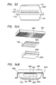
- Fig. 3 shows a typical example of a semiconductor device having elements connected and sealed by TAB method. Briefly, this method is an automatic bonding method making use of tape carrier system. Referring to Fig. 3, after the carrier film substrate 16 and a semiconductor element 4 are located, the inner lead portion 17 of the carrier film substrate 16 and the connecting portion 5 of the semiconductor element 4 are heat-bonded. Thereafter, the inner lead 17 and the semiconductor element 4 are sealed by resins 20 and 21.
- Fig. 4 shows a typical example of a semiconductor device having elements connected and sealed by CCB method. This method, which also is referred to as flip chip bonding method, will be explained with reference to Fig. 4.
- a semiconductor element 4, which is beforehand provided with solder bumps 31, are located and placed on a circuit board 32. Thereafter, the solder is heated and molten so that the semiconductor element 4 is connected to the circuit board 32. Then, after washing away the flux, the semiconductor element 4 is sealed so that a semiconductor device 9 is obtained.
- An insulating film 71 of, for example, polyimide is formed on the portion of a first semiconductor element 4 other than the connecting portion 5, while a metallic member 70 such as of Au is placed on the connecting portion 5. Then, the exposed surfaces 73, 72 of the metallic member 70 and the insulating film 71 are flattened.
- an insulating film 71 ⁇ of, for example, polyimide is formed on the portion of a second semiconductor element 4 ⁇ other than the connecting portion 5 ⁇ , while a metallic member 70 ⁇ such as of Au is placed on the connecting portion 5. Then, the exposed surfaces 73 ⁇ , 72 ⁇ of the metallic member 70 ⁇ and the insulating film 71 ⁇ are flattened.
- first semiconductor device 4 and the second semiconductor device 4 ⁇ are located with respect to each other as shown in Fig. 6 and heat and pressure are applied to both semiconductor devices, whereby the connecting portions 5 and 5 ⁇ of the first and second semiconductor elements 4 and 4 ⁇ are connected to each other through the metallic members 70, 70 ⁇ .
- a first circuit board 75 and a second circuit board 75 ⁇ are located with respect to each other through the intermediary of an anisotropic conductive film 78 having conductive particles dispersed in an insulating material 77. Then, pressure or pressure and heat are applied to the first and second circuit boards, whereby both circuit boards are connected at their connecting portions 76 and 76 ⁇
- a first circuit board 75 and a second circuit board 75 ⁇ are located with respect to each other through the intermediary of an elastic connector 83 composed of an insulating material 81 and metallic wires of Fe. Cu or the like unidirectionally disposed in the insulating material 81. Then, pressure is applied to both circuit boards, whereby both circuit boards are connected at their connecting portions 76, 76 ⁇ .
- the present invention may provide highly concentrated multiple connections and an improvement in various properties such as a thermal property as well as replacement of connection from the conventional connecting methods.
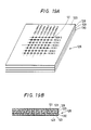
- It is another object to provide an element for use in electrical connection comprising a holding member having an insulator and metallic powder dispersed in said insulator and a conductive member laid in said holding member said conductive member having an end which is exposed on the surface of one side of said holding member and another end which is exposed on the surface of the other side of said holding member.
- It is a further object to provide an element for use in electrical connection comprising a holding member having an insulator and metallic fiber dispersed in said insulator and a conductive member laid in said holding member said conductive member having an end which is exposed on the surface of one side of said holding member and another end which is exposed on the surface of the other side of said holding member.
- It is a further object to provide an element for use in electrical connection comprising a holding member having an insulator and metallic body laid in said insulator and a conductive member laid in said holding member said conductive member having an end which is exposed on the surface of one side of said holding member and another end which is exposed on the surface of the other side of said holding member.
- It is a further object to provide an element for use in electrical connection comprising a holding member having an inorganic insulator and a conductive member laid in said holding member said conductive member having an end which is exposed on the surface of one side of said holding member and another end which is exposed on the surface of the other side of said holding member.
- It is a further object to provide an element comprising a holding member a conductive member laid in said holding member said conductive member having one end which is exposed on the surface of one side of said holding member and another end which is exposed on the surface of the other side of said holding member a first electrical circuit member having a first connecting portion to which said one end of said conductive member is connected and a second electrical circuit member having a second connecting portion to which said another end of said conductive member is connected said first connecting portion and said one end and/or said second connecting portion and said another end being connected by alloying.
- an electrical circuit device comprising a holding member a conductive member laid in said holding member said conductive member having one end which is exposed on the surface of one side of said holding member and another end which is exposed on the surface of the other side of said holding member a first electrical circuit member having a first connecting portion to which said one end of said conductive member is connected a second electrical circuit member having a second connecting portion to which said another end of said conductive member is connected and a sealing element for sealing at least one of said first electrical circuit member and said second electrical circuit member by laying therein.
- an electrical circuit device comprising a holding member a conductive member laid in said holding member said conductive member having one end which is exposed on the surface of one side of said holding member and another end which is exposed on the surface of the other side of said holding member a first electrical circuit member having a first connecting portion to which said one end of said conductive member is connected a second electrical circuit member having a second connecting portion to which said another end of said conductive member is connected and a cap for cap-sealing at least one of said first electrical circuit member and said second electrical circuit member.
- a first electric circuit component and a second electric circuit component are connected to each other through an electrical connecting member or electrical bonding intermediary.
- the present invention provides an electric circuit device composed of a first electric circuit component provided with bonding portions, a second electric circuit component having bonding areas, and an electric bonding intermediary placed and connected between the first and second electric circuit components so as to attain electrical connection between the first and second electric circuit components at their bonding areas
- the electric bonding intermediary includes a pluralilty of conductive members of embedded in holding member in such a manner that they are electrically insulated from one another, with their one ends exposed in a first surface of the holding member facing the first electric circuit component while their other ends are exposed in a second surface of the holding member facing the second electric circuit component, the ends of the conductive members exposed in the same side as the first electric circuit component are connected to the bonding areas of the first electric circuit component, while the ends of the conductive members exposed in the same side as the second electric circuit component are connected to the bonding areas of the second electric circuit component.
- the electric bonding intermediary may have a single-layered structure or may have a laminated structure composed of two or more layers.
- the electric circuit device of the present invention is composed of a first electric circuit component which may be any one of the above-mentioned devices or circuit boards and a second electric circuit component which also may be any one of the above-mentioned devices or circuit boards.
- one or more electrical circuit component to be connected to the electrical bonding intermediary may be provided on one of the surfaces of the holding member.
- any type of electric parts having bonding areas are usable as the electric circuit component in the present invention, regardless of the number of the bonding areas, though the advantage brought about by the invention becomes more appreciable as the number of the bonding area is increased. It is also to be understood that there is no restriction in the positions of the bonding areas. It is to be noted, however, that the advantage of the present invention becomes more remarkable when the bonding areas are located in the inner portion of the electric circuit component.
- the conductive member according to the invention includes, for example metallic material.
- Gold is used most suitably as the material of the metallic members of the electric bonding intermediary used in the present invention, but other metals or alloys can also be used satisfactorily, such as Ag, Be, Ca, Mg. Mo, Ni, W, Fe, Ti, In, Ta, Zn, Cu, Al, Sn, Pb-Sn, and so forth.
- the same metals or different metals may be present in the same electrical bonding intermediary.
- One of the metallic members of the electrical bonding intermediary may be formed by the same metals or alloys, or different metals or alloys.
- the material in which the organic and/on inorganic material is included in the metal may be used as a metallic member if it has the electrical conductivity.
- the conductive material combined with organic and inorganic materials may also used. It is to be noted that the super conductive material may be used as the conductive member.
- the metallic member can have any desired cross-sectional shape such as circular, square of other shape.
- the diameter or size of the metallic member also can be selected freely.
- the diameter is determined to be not smaller than 20 ⁇ m, taking into account the pitch of the bonding areas on the electric circuit components, through it may be determined to be not greater than 20 ⁇ m.
- the exposed portion of the metallic member may be flush with the insulating holder or may be projected therefrom.
- the arrangement may be such that the metallic members project only at one side of the holder or at both sides thereof.
- the projected ends of the metallic members may be shaped in the form of bumps.
- the pitch of the metallic members may be equal to or smaller than the pitch of the bonding areas of the electric circuit components.
- the connection between the electric circuit component and the electric bonding intermediary can be attained without requiring precise location of these two members.
- metallic member extends vertically through the insulating holder.
- the metallic members may extend slantwise from the end adjacent to the first electric circuit component to the end adjacent to the second electric circuit component.
- the holding member of the electric bonding intermediary used in the present invention may include, for example, a member using electrically insulating material.
- the organic and inorganic material may be used as the electrically insulating material.
- the metallic material may also be used when it is treated to electrically insulate the conductive members each other.
- one kind or a plurality of kinds of powder, fiber or material having desired shape all of which comprise the inorganic or metallic material may be dispersed in the organic material.
- one kind or a plurality of kinds of power, fiber or material having desired shape all of which comprise the organic or metallic material may be dispersed in the inorganic material.
- one kind or a plurality of kinds of powder, fiber or material having desired shape all of which comprise the organic or inorganic material may be dispersed in the metallic material.
- the holding member comprises the metallic material
- elecrically insulating material such as resin may be provided between the electrically conductive member and the holding member.
- an insulating resin as organic material can be used satisfactorily.
- the type of the insulating resin is not limited. Both thermosetting, ultraviolet curing resin and thermoplastic resins can be used equally well.
- resins suitably used are polyimide resin, polyphenylene sulfide resin, polyether sulfone resin, polyether imide resin, polysulfone resin, silicone reisn, fluororesin, polycarbonate resin, polydiphenylether resin, polybenzyl imidazole resin, phenol resin, urea resin, melamine resin, alkyd resin, epoxy resin, polyamideimide resin, polypropylene resin, polyvinyl chloride resin, polystylene resin, methacrylate methyl, polyphenylene oxide, methacrylic resins, vinylidene chloride, and so forth.
- the resin used as the material of the insulating holder has a thermal expansion coefficient which well approximates that of the circuit substrate so that any trouble attributable to thermal expansion and contraction may be eliminated, thus assuring high reliability of the product device.
- the electric bonding intermediary used in the present invention can have various forms as exemplarily shown in I to VI below.
- This electric bonding intermediary has a plurality of conductive member (to be referred "metallic members” hereinafter) embedded in an insulator.
- the metallic members are electrically insulated from one another by the material of the insulator. One ends of the metallic members are exposed in the face of the insulator adjacent to the first electric circuit component, while other ends are exposed in the face of the insulator adjacent to the second electric circuit component.
- This electric bonding intermediary has a plurality of metallic members embedded in an insulator.
- the metallic member are elecrically insulated from one another by the material of the insulator.
- One ends of the metallic members are exposed in the face of the insulator adjacent to the first electric circuit component, while other ends are exposed in the face of the insulator adjacent to the second electric circuit component.
- Fillers such as powder particles and/or fibers of a metal or an alloy are dispersed in the insulator.
- the electric bonding intermediary of this example has an insulator in which are dispersed fillers such as powder particles and/or fibers of one, two or more of these metals and alloys. That is, the insulator may contain either one or both of powder particles and the fibers.
- the powder particles and the fibers may or may not have been subjected to a surface treatment such as plating.
- Factors such as the size, shape, location and quantity of the powder particles and fibers dispersed in the insulator may be determined suitably such that the dispersed powder particles and the fibers do not cause troubles such as mutual contact between adjacent metallic members, short-circuiting, breakdown of the metallic members, and so forth. It is, however, preferred that the size of the powder particles or the fibers is smaller than the distance between adjacent metallic members, so that adjacent metallic members may not electrically contact with each other through the powder particles and fibers.
- the dispersed powder particles and/or the fibers may be exposed to the outside provided that they do not impair the desired electrical connection between the electric circuit component.
- the powder particles, as well as the fibers may or may not contact with adjacent ones.
- the dispersion of the powder particles or the fibers can be effected by adding the powder particles and/or the fibers to the resin and then mixing the resin, although other dispersion method may be employed.
- This electric bonding intermediary features a high heat conductivity by virtue of the dispersion of the powder particles and/or fibers of a metal or an alloy.
- This type of electric bonding intermediary therefore, can suitably be used in such a case that the first electric circuit component produces much heat, while the second electric circuit component is comparatively resistant to heat. In such a case, the heat generated in the first electric circuit component is transmitted through the electric bonding intermediary to the second electric circuit component and then radiated from the latter. It is thus possible to obtain an electric circuit device having superior heat radiation characteristic.
- This electric bonding intermediary has a plurality of metallic members embedded in an insulator.
- the metallic members are electrically insulated from one another by the material of the insulator.
- One ends of the metallic members are exposed in the face of the insulator adjacent to the first electric circuit component, while other ends are exposed in the face of the insulator adjacent to the second electric circuit component.
- Fillers such as powder particles and/or fibers of an inorganic material are dispersed in the insulator.
- the term "inorganic material” in this specification is used to generally mean a material other than metallic materials and organic materials.
- examples of such inorganic material are ceramics such as SiC, BeO, B2C, TaC, TiB2, CrB2, TiN, BP, BN, AlN, Si3N4 and SiO2, diamond, C, B, glass, and so forth.
- the electric bonding intermediary of this example has an insulator in which are dispersed powder particles and/or fibers of one, two or more of these inorganic materials. That is, the insulator may contain either one or both of powder particles and the fibers.
- Factors such as the size, shape, location and quantity of the powder particles and fibers dispersed in the insulator may be determined suitably such that the dispersed powder particles and the fibers do not cause troubles such as mutual contact between adjacent metallic members, short-circuiting, breakdown of the metallic members, and so forth. It is, however, preferred that the size of the powder particles or the fibers is smaller than the distance between adjacent metallic members, so that adjacent metallic members may not electrically contact with each other through the powder particles and fibers.
- the dispersed powder particles and/or the fibers may or may not be exposed to the outside.
- the powder particles, as well as the fibers, may or may not contact with adjacent ones.
- the dispersion of the powder particles or the fibers can be effected by adding the powder particles and/or the fibers to the resin and then mixing the resin. although other dispersion method may be employed.
- This electric bonding intermediary features a high heat conductivity from the first electric circuit component to the second electric circuit component, by virtue of the dispersion of the powder particles and/or fibers.
- This type of electric bonding intermediary therefore, can suitably be used in such a case that the first electric circuit component produces much heat, while the second electric circuit component is comparatively resistant to heat. In such a case, the heat generated in the first electric circuit component is transmitted through the electric bonding intermediary to the second electric circuit component and then radiated from the latter. It is thus possible to obtain an electric circuit device having superior heat radiation characteristic.
- the inorganic powder particles or fibers produce only small thermal stress when the electric bonding intermediary is heated. It is therefore possible to obtain high reliability of the electric circuit components and, hence, high reliability of semiconductor devices.
- This electric bonding intermediary has a plurality of metallic members embedded in an insulator.
- the metallic members are electrically insulated from one another by the material of the insulator. One ends of the metallic members are exposed in the face of the insulator adjacent to the first electric circuit component, while other ends are exposed in the face of the insulator adjacent to the second electric circuit component.
- Metallic pieces and/or inorganic pieces of any desired forms are embedded in the insulator.
- the metallic pieces and/or inorganic pieces embedded in the insulator may have any suitable form such as tabular form, rod-like form with various cross-sectional shapes, spheres, and so forth.
- the electric bonding intermediary of this example has an insulator which contains two or more of these inorganic materials. That is, the insulator may contain at least one kind of metallic filler and/or at least one kind of inorganic filler.
- Factors such as the size, shape, location and quantity of the metallic pieces and/or the inorganic pieces in the insulator may be determined suitably such that the dispersed metallic or inorganic pieces do not cause troubles such as mutual contact between adjacent metallic members, short-circuiting, breakdown of the metallic members, and so forth.
- the metallic fillers and/or the inorganic fillers need not be uniformly dispersed. Namely, they may be dispersed locally only in limited regions in the insulator. In other words, the insulator may have local regions which are devoid of such fillers.
- the metallic pieces and/or inorganic pieces may or may not be exposed to the outside and may or may not contact with adjacent ones.
- This electric bonding intermediary features a high heat conductivity from the first electric circuit component to the second electric circuit component and vice versa, by virtue of the presence of the metallic pieces or inorganic pieces of desired shape in the insulator.
- This type of electric bonding intermediary therefore, can suitably be used in such a case that the first electric circuit component produces much heat, while the second electric circuit component is comparatively resistant to heat. In such a case, the heat generated in the first electric circuit component is transmitted through the electric bonding intermediary to the second electric circuit component and then radiated from the latter. It is thus possible to obtain an electric circuit device having superior heat radiation characteristic.
- the insulator contains pieces of an inorganic material which has a thermal expansion coefficient approximating that of the electric circuit component, so that the insulator of the electric bonding intermediary exhibits a thermal expansion coefficient approximating that of the electric circuit component, thereby preventing undesirable effects such as rupture of the insulator or the metallic members, as well as degradation of the characteristics of the electric circuit part, thus assuring high reliability of the semiconductor device.
- This example of the electric bonding intermediary offers remarkable advantage particularly when a large difference of thermal expansion coefficient exists between the first electric circuit component and the second electric circuit component.
- the metallic fillers embedded in the insulator effectively prevents any noise of the electric circuit component from leaking outside, while excluding external noises.
- This electric bonding intermediary has a plurality of metallic members embedded in a metallic or alloy holder through the intermediaries of insulating members. One ends of the metallic members are exposed in the face of the holder adjacent to the first electric circuit component, while other ends are exposed in the face of the holder adjacent to the second electric circuit component.
- Examples of the metallic or alloy material suitably used as the material of the holder are Ag, Cu, Au, Al, Be, Ca, Mg, Mo, Ni, Si, W, Fe, Ti, In, Sn, Zn, and so forth, as well as alloys of these metals.
- each metallic member and the holder may be realized in various methods.
- the holder when the holder is made of a material which can be anode-oxidated, e.g., Al or Ti, bores are formed in predetermined portions of the holder so as to receive the metallic members and then the holder is subjected to anode oxidation so that anode-oxidation films which effectively serve as insulating layers are formed on the surfaces of the bores.
- a material which can be anode-oxidated e.g., Al or Ti
- bores are formed in predetermined portions of the holder so as to receive the metallic members and then the holder is subjected to anode oxidation so that anode-oxidation films which effectively serve as insulating layers are formed on the surfaces of the bores.
- the insulating material by subjecting the holder to flame spraying or evaporation with, for example, ceramics, after forming bores in the holder.
- the insulating material also may be formed by applying a resin to the surfaces of bores formed in the holder.
- a suitable treatment such as oxidation, nitriding, boriding or carburizing is effected on the boundaries between the metallic members and the holder so that the metallic members are electrically isolated from the holder.
- the holder and the metallic member are made of the same metal or alloy.
- the formation of the insulating material may be effected on both sides of the electric bonding intermediary, or only on the side of the electric bonding intermediary adjacent to the first electric circuit component or the side adjacent to the second electric circuit component.
- an intermediary member made of a resin or an inorganic material is disposed between each metallic member and the wall of the bore in the holder receiving each metallic member.
- a tubular member is fitted in each bore so as to fit on each metallic member.
- the intermediary member is made of a resin
- the invention does not restrict the type of resin.
- an electrically insulating resin material can suitably be used.
- resins suitably used are polyimide resin, polyphenylene sulfide resin, polyether sulfone resin, polyether imide resin, polysulfone resin, silicone resin, fluororesin, polycarbonate resin, polydiphenylether resin, polybenzyl imidazole resin, phenol resin, urea resin, melamine resin, alkyd resin, epoxy resin, polyamideimide resin, polypropylene resin, polyvinyl chloride resin, polystylene resin, and so forth.
- the resin may contain fillers such as powder particles and/or fibers of a metallic material or an inorganic material dispersed therein.
- the invention does not limit the shape, size and location of the powder particles or fibers, although due consideration has to be paid such as to prevent any electrical contact between the metallic members and the holder through such powder particles or fibers. It is also possible to disperse tabular member, rod-shaped members or spherical members of a metallic or inorganic material in the resin. The locations, shapes and sizes of the tabular, rod-shaped or spherical members can also be selected freely also in this case.
- the inorganic material may be one selected from ceramics such as SiO2, B2O3, Al2O3, Na2O, K2O, CaO, ZnO, BaO, PbO, Sb2O3, As2O3, La2O3, ZrO2, BaO, P2O5, TiO2, MgO, SiC, BeO, BP, BN, AlN, B4C, TaC, TiB2, CrB2, TiN, Si3N4, and Ta2O5, diamond, C, B, glass, and so forth.
- ceramics such as SiO2, B2O3, Al2O3, Na2O, K2O, CaO, ZnO, BaO, PbO, Sb2O3, As2O3, La2O3, ZrO2, BaO, P2O5, TiO2, MgO, SiC, BeO, BP, BN, AlN, B4C, TaC, TiB2, CrB2, TiN, Si3N4, and Ta2O5, diamond, C, B, glass, and so forth.
- the resin used has a high heat conductivity so that heat produced by the semiconductor device may be radiated through the resin or inorganic material.
- This electric bonding intermediary features a high heat conductivity from the first electric circuit component to the second electric circuit component and vice versa, by virtue of the holder which is made of a metal or an alloy.
- This type of electric bonding intermediary therefore, can suitably be used in such a case that the first electric circuit component produces much heat, while the second electric circuit component is comparatively resistant to heat. In such a case, the heat generated in the first electric circuit component is transmitted through the electric bonding intermediary to the second electric circuit component and then radiated from the latter. It is thus possible to obtain an electric circuit device having superior heat radiation characteristic.
- the metallic or alloy holder effectively prevents any noise of the electric circuit component from leaking outside, while excluding external noises.
- This electric bonding intermediary has metallic members embedded in a holder made of an inorganic material. One ends of the metallic members are exposed in the face of the holder adjacent to the first electric circuit component, while the other ends are exposed in the face adjacent to the second electric circuit component.
- Examples of the resin suitable for use as the material of the holder are SiO2, B2O3, Al2O3, Na2O, K2O, CaO, ZnO, BaO, PbO, Sb2O3, As2O3, La2O3, ZrO2, BaO, P2O5, TiO2, MgO, SiC, BeO, BP, BN, AlN, B4C, TaC, TiB2, CrB2, TiN, Si3N4, and Ta2O5, diamond, C, B, glass, and so forth.
- the inorganic material of the holder of the electric bonding intermediary can contain fillers such as of a metal, resin or the like dispersed therein in such a manner as to avoid short-circuiting between metallic members.
- an intermediate member made of an electrically insulating material such as an inorganic material or a resin is placed between each electric member and the holder so as to electrically insulate the metallic member.
- the use of the intermediate member is not necessary when the inorganic material used as the material of the holder is a non-conductive material. In such a case, however, an intermediate member such as of a metal, an inorganic material or a resin may be used for the purpose of improving conduction of heat thereby enhancing heat radiation.
- Examples of the metallic material suitably used as the material of such an intermediate member are Ag, Cu, Au, Al, Be, Ca, Mg, Mo, Ni, Si, W, Fe, Ti, In, Sn, Zn and so forth, as well as alloys of thee metals.
- thermosetting resin any thermosetting resin, ultraviolet setting resin and thermoplastic resin can be used suitably.
- the resins suitably used are polyimide resin, polyphenylene sulfide resin, polyether sulfone resin, polyether imide resin, polysulfone resin, silicone resin, fluororesin, polycarbonate resin, polydiphenylether resin, polybenzyl imidazole resin, phenol resin, urea resin, melamine resin, alkyd resin, epoxy resin, polyamideimide resin, polypropylene resin, polyvinyl chloride resin, polystylene resin, and so forth.
- the resin contain metallic and/or inorganic fillers in the form of powder particles and.or fibers dispersed therein.
- the shape, size, location and quantity of such fillers are not limited, although due consideration has to be paid to avoid any electrical contact between the metallic members and the holder through such fillers.
- the resin also may contain at least one of tabular fillers, rod-shaped fillers and spherical fillers of either one or both of a metallic material and an inorganic material.
- the shape, size, location and quantity of such fillers also are unlimited.
- the fillers in the form of powder particles, fibers, tabular members and spherical members may contact with one another. These fillers also may partially exposed to the outside of the holder. It is, however, essential that the fillers are dispersed in such a manner as to avoid any short-circuiting between different metallic members, breakage of the metallic members, and other inconveniences.
- the metal, resin or the inorganic material used as the material of the intermediate member has high heat conductivity so that the heat generated in the semiconductor device may efficiently radiate through the intermediate member.
- the holder is made of an inorganic material which usually has an appreciable level of heat conductivity, so that efficient conduction of heat from the first electric circuit component to the second electric circuit component and vice versa is assured.
- this example of the electric bonding intermediary features a high level of heat conductivity and, therefore, can suitably be used in such cases where a component having a large heat generation is used as the first electric circuit component while the second electric circuit component has a high durability to heat. In such cases, the heat generated in the first electric circuit component is quickly transmitted to the second electric circuit component and efficiently radiated therefrom. It is thus possible to obtain an electric circuit device having superior heat radiation characteristics.
- the holder of the bonding intermediary made of an inorganic material exhibits thermal expansion which well approximates that of the substrates of the electric circuit components which are usually made of an inorganic material.
- the thermal stress is sufficiently suppressed to avoid occurrence of above-mentioned failure or trouble, thus ensuring high level of reliability of product electric circuit device, e.g., a semiconductor device.
- the bonding between the first and second electric circuit components through the bonding intermediary of the invention can broadly be sorted into the following three types A, B and C.
- the first and the second electric circuit components are bonded to each other through the bonding intermediary.
- the bonding is effected by any known method such as a mechanical method consisting in pressing the electric circuit components together while placing the bonding intermediary therebetween.
- the bonding areas of the first electric circuit component are bonded by alloying to the ends of the metallic members exposed in the side of the bonding intermediary adjacent to the first electric circuit component or, alternatively, the bonding areas of the second electric circuit component are bonded by alloying to the ends of the metallic members exposed in the side of the bonding intermediary adjacent to the second electric circuit component.
- alloying of the bonding areas is effected on either one of the first electric circuit component and the second electric circuit component.
- the alloying may simply be effected by placing corresponding bonding areas in contact with each other and heating them at a suitable temperature. As a result of the heating, diffusion of atoms and other phenomenon take place to form a solid-solution or intermetallic compound layer at the boundary, thus alloying and bonding the bonding areas of the two members.
- the alloying heating temperature preferably ranges between 200 and 350°C.
- the bonding between the bonding intermediary and the other electric circuit component which is not alloyed may be achieved by any suitable method, e.g., by pressing them together.
- the alloying of the bonding area for the electrical connection is effected on only one of the first and the second circuit components. Therefore, when one of the first and the second circuit components involves a risk of degradation due to heat applied during alloying, such electric circuit component is bonded by other means than alloying, e.g., by mechanical pressing, while the bonding by alloying is conducted with the other electric circuit component.
- the occasion may demand that either one of the electric circuit components is freely demountable even after the completion of the electric circuit device.
- the electric circuit component which is to be demountable is connected by a mere pressing, without being alloyed.
- the bonding areas of the first electric circuit component are bonded by alloying to the ends of the metallic members exposed in the side of the bonding intermediary adjacent to the first electric circuit component and, at the same time, the bonding areas of the second electric circuit component are bonded by alloying to the ends of the metallic members exposed in the side of the bonding intermediary adjacent to the second electric circuit component.
- alloying of the bonding areas is effected on both of the first electric circuit component and the second electric circuit component.
- the alloying method may be similar to that used in the type B of bonding.
- both electric circuit components are rigidly (strongly) bonded together, by virtue of the alloying bonding between the bonding intermediary and the bonding areas of both electric circuit components.
- electric circuit device of superior mechanical strength can be produced with extremely low rate of rejection.
- the resistance of the electrical connection between both electric circuit components is reduced as compared with the type B of bonding which employs alloying of only one of the electric circuit components, because both the first and the second electric circuit components are bonded through alloying.
- connection therebetween by alloying has the same crystal structure as the conductive member and the connecting portions.
- An example of the alloying is heating at an appropriate temperature after contacting an edge of the conductive member with a connecting portion corresponding to the edge. The heating causes diffusion of atoms near the contact. The diffusion area becomes an alloy condition to form the connection.
- connection is an alloy of the metals.
- the alloying process is heating at an appropriate temperature after contacting an edge of the conductive member and the connecting portion corresponding to the edge. The heating causes diffusion of atoms near the contact area, forming a layer of a solid solution or an intermetallic compound. The layer becomes the connection.
- connection becomes their alloy.
- the conductive member and the connecting member be an alloy or alloys at their contacting areas. But the other areas of the members can be a state in which a resin is impregnated in glass fibers.
- the contact areas have small surface roughness, preferably less than 0.3 ⁇ m, in order to enhance a strength of the connection. Furthermore, a layer of plating of an easily alloyed metal or an alloy may be given on a surface to be connected.
- the electric circuit parts may be sealed by a sealing material.
- the sealing may be effected on one or a plurality of the electric circuit parts.
- thermoplastic resin may be used as a sealing material.
- the thermoplastic material can be selected from the following: polyimide, polyphenylene sulfide, polyether sulfone, polyether imide, polysulfone, fluororesin, polycarbonate, polydiphenylether, polybenzylimidazole, polyamidimide, polypropylene, polyvinyl chloride, polystyrene, methyl methacrylate, other resins.
- the sealing may be one of the above resins or the resin with dispersion of either or both of powers and fibers of one or more of metals, alloys and inorganic materials.
- the dispersion may be performed by adding the powders or fibers to the resin and agitating them. However, the dispersion may also be done by any other method.
- the metals or the alloys may be selected from Ag, Cu, Au, Al, Be, Ca, Mg, Mo, Fe, Ni, Si, Co, Mn, W, etc.
- the inorganic materials may be selected from ceramics: SiO2, B2O3, Al2O3, Na2O, K2O, CaO, ZnO, BaO, PbO, Sb2O3, As2O3, La2O3, ZrO2, BaO, P2O5, TiO2, MgO, SiC, BeO, BP, BN, AlN, B4C, TaC, TiB2, CrB2, TiN, Si3N4, Ta2O5, etc.; diamond; glass; carbon; boron; and other inorganic materials.
- a size, a shape, a dispersion position, and an amount of dispersed powders and fibers may be chosen within a range where metal members embedded in insulator are without contact or short-circuit with each other through the powders or the fibers. It is, however, preferable that the size of the powders and the fibers is smaller than a distance between two neighboring metal member. That is, the electrically conductive members should not preferably contact with each other even through the powders and the fibers.
- the powders and the fibers may or may not be exposed outside the insulator. The powders and the fibers may or may not contact with each other.
- the electric circuit device has a superior heat dissipation because heat generated in the electric circuit parts is transmitted earlier to the outside. Further, the electric circuit device has a high shielding property.
- the sealing process is i) setting in a molding cavity the electric circuit member which comprises an electrically connecting member and electric circuit members connected to the connected member, ii) injecting a sealing material into the cavity by injection molding to seal them.
- the electric circuit member may be sealed by such injection molding, extrusion molding, cast molding, blow molding and any other method.
- a plate may be sticked to at least one of surfaces of the sealings.
- the plate may also be sticked to another face of the electric circuit part opposite the electrically connecting member. It's unnecessary that the plate is sticked to all the electric circuit parts. It is sufficient that a plate is sticked to at least a portion of at least one electric circuit member.
- At least one plate or a plate assembly may be placed near a face of the circuit part opposite the connecting member or a side face thereof. Such plate is not always placed near all the electric circuit parts. It is essential that a plate is placed near at least one electric circuit part.
- the plate may be made of any material different from that of the sealing.
- the plate has a thickness, e.g. preferably of 0.05 to 0.5 mm in case of a stainless steel plate.
- the plate may be sticked by an adhesive. Any other method can be employed if the plate may hold the electric circuit device.
- the thus disposed plate may prevent a stress concentration due to an interval stress or an external stress, and as a result cracks caused by the stress concentration.
- the plate lengthens a pass from the outside to the electric circuit parts, thus making it difficult for foreign materials such as water to reach the electric circuit parts. This enhances a reliability of the device.
- the plate is made of metals such as stainless steel; ceramics, carbon and diamond with high heat conductivity, heat generated by the electric circuit parts may be dissipated fast to the outside, thus resulting in providing an electric circuit device superior in heat dissipation property.
- heat generated by the electric circuit parts may be dissipated fast to the outside, thus resulting in providing an electric circuit device superior in heat dissipation property.
- the plate is made of a metal, noises from the outside and electromagnetic noises generated from the electric circuit parts may effectively be shielded, providing an electric circuit device superior in a shielding property.
- the electric circuit device of the present invention may have a cap for cap-sealing the electric circuit parts.
- the "cap-sealing” means covering and sealing the electric circuit parts to provide an internal hollowed space.
- the cap may be provided for one or plural electric circuit parts.
- the sealing should preferably be effected such that the electric circuit parts are held tight on the electrically connecting member.
- an inside face of the cap is shaped corresponding to an outer surface of the electric circuit parts and is made contacting the outer surface of the circuit part to effect the cap-sealing.
- the cap may be sticked to an electric circuit part or another cap which is provided for another electric circuit part to be cap-sealed if any by an adhering method with an adhesive, a mechanical method, a fusion, and any other method.
- the cap may be made of either of metals, inorganics or organics.
- the metals may be, for example, ceramics such as SiO2, B2O3, Al2O3, Na2O, K2O, CaO, ZnO, BaO, PbO, Sb2O3, As2O3, La2O3, ZrO2, BaO, P2O5, TiO2, MgO, SiC, BeO, BP, BN, AlN, B4C, TaC, TiB2, CrB2, TiN, Si3N4, Ta2O5; diamond; glass; carbon; boron; others.
- ceramics such as SiO2, B2O3, Al2O3, Na2O, K2O, CaO, ZnO, BaO, PbO, Sb2O3, As2O3, La2O3, ZrO2, BaO, P2O5, TiO2, MgO, SiC, BeO, BP, BN, AlN, B4C, TaC, TiB2, CrB2, TiN, Si3N4, Ta2O5; diamond; glass; carbon; boron; others.
- a metal material In the inorganic materials a metal material, a resin or other material may be dispersed.
- the organic materials may be any of thermosetting resins, ultraviolet curable resins, and thermoplastic resins.
- either of both of powders and fibers of metals and inorganics may be dispersed in the resins. If dispersed, a shape, a size, a dispersion position and an amount of the dispersed powders and the fibers are not limited. Also, at least one of plates, rods and balls of either or both of metals and/or inorganics may be embedded within the resins. A location of the embedding, a shape, a size and an amount of the embedded plates rods and/or balls are not limited. The powders, the fibers, the plates, the rods and the balls may contact with each other in the resins.
- an adjusting member may be disposed between the cap and the electric circuit part.
- the adjusting member may be made of either of metals, inorganics and organics, which is preferably elastic.
- a shape of the adjusting member is not limited to a specific one if it can adjust a height of the electric circuit part.
- the intervention of the adjusting member between the electric circuit part and the cap allows adjustment of the height of the electric circuit part, resulting in avoiding preparation of various inside shapes of the cap fitting the electric circuit part. Also, deviation of dimensions upon assembling may be adjusted by the adjusting member. Such an adjusting member is especially effective to the cap-sealing of various electric circuit devices.
- the first embodiment is an electric circuit device which includes a circuit board 101 as a first electric circuit component with bonding areas 102, a second circuit board 104 as a second electric circuit component with bonding areas 105, and an electric bonding intermediary 125 placed between both circuit boards 101, 104 and connected to the bonding areas 102, 105 thereby providing electrical connection between the first and the second circuit boards, wherein the electric bonding intermediary 125 includes an insulator 111 and a plurality of metallic members 107 of a metal or an alloy embedded in the insulator 101 in such a manner that the metallic members 107 are electrically insulated from one another and that one ends of the metallic members 107 are exposed on one side of the insulator adjacent to the first circuit board 101 while other ends are exposed on the other side of the insulator 111 adjacent to the second circuit board 104, and wherein bonding is attained by alloying between the bonding areas 102 of the first circuit board 101 and the ends of the metallic members 107 exposed to the same side as the first circuit board 101 or, alternatively
- Figs. 10A to 10C illustrate an example of the process for producing the electric bonding intermediary 125 used in the first embodiment.
- a metallic wire 121 made of a metal such as gold or a suitable alloy and having a diameter of about 20 ⁇ m is turned around a plurality of bars 122 at a pitch of 40 ⁇ m, and the wire 121 together with the bars 122 are embedded in a resin body 123 such as of polyimide resin.
- the resin after setting serves as an insulator.
- the resin body 123 is sliced as indicated by broken lines 124, whereby a plurality of electric bonding intermediary 125 are obtained as shown in Figs. 10B and 10C.
- the metallic wires 121 as the metallic members are insulated from one another by the resin 123. It will be seen that one ends of the metallic wires 121 are exposed on the surface of the electric bonding intermediary 125 adjacent to the first circuit board 101, while the other ends of the same are exposed on the surface of the electric bonding intermediary 125 adjacent to the second circuit board 104. These exposed portions of the metallic wires 121 constitute bonding areas 108, 109 where the bonding intermediary is to be bonded to the circuit boards 101 and 104.
- the first and the second circuit boards 101 and 104 are then set together with the electric bonding intermediary 125 interposed therebetween.
- the circuit boards 101, 104 are provided with a multiplicity of bonding areas 102, 105 within the areas thereof.
- the bonding areas 102 of the first circuit board 101 are exposed at positions corresponding to the bonding areas 105 of the second circuit board 104 and the bonding areas 108, 109 of the electric bonding intermediary 125.
- the first circuit board 101 and the electric bonding intermediary 125 are located with respect to each other such that the bonding areas 102 on the first circuit board 101 and the bonding areas 108 of the electric bonding intermediary 125 are aligned, and then the aligned bonding areas are mutually alloyed.
- the second circuit board 104 and the electric bonding intermediary 125 are located with respect to each other such that the bonding areas 105 on the second circuit board 104 and the bonding areas 109 of the electric bonding intermediary 125 are aligned, and then the aligned bonding areas are mutually alloyed.
- the other circuit board is connected by, for example, mechanical pressing.
- the first embodiment can be assembled by either one of the following two methods (1) and (2).
- Figs. 11A and 11B show a second embodiment of the invention.
- the second embodiment was constructed by using, as the first electric circuit component, a circuit board 51 having bonding areas 52 and, as the second electric circuit component, a semiconductor device 4 having a multiplicity of bonding areas 5 within the area thereof.
- the bonding by alloying was effected to achieve electrical connection between the bonding areas 5 of the semiconductor device 4 and the bonding areas 54 of the electric bonding intermediary 125.
- the electric bonding intermediary 125 was designed to be equal in size to the semiconductor device 4.
- a lead frame 55 was connected to the underside of the circuit board 51.
- Fig. 12 shows a third embodiment of the present invention.
- the third embodiment was constructed by using the semiconductor device 4 as the first electric circuit component and the circuit board 51 as the second electric circuit component.
- a lead frame 1 was connected to the upper side of the circuit board 51 and then the upper surface of the thus obtained assembly was sealed with a resin 63.
- Fig. 13 shows a fourth embodiment of the invention.
- the fourth embodiment was constructed by using the semiconductor device 4 as the first electric circuit component and another semiconductor device 4 ⁇ as the second electric circuit component.
- the electric bonding intermediary was designed to correspond in size to the semiconductor device 4 ⁇ and a lead frame 1 was connected to the ends of the metallic members of the bonding intermediary 125 exposed to the same side as the semiconductor device 4.
- Figs. 14A and 14B show a fifth embodiment of the invention.
- circuit boards 101, 104 which are coated by insulating films 103, 106 at portions other than the bonding areas, are used as the first and second electric circuit components, respectively.
- the exposed ends of the metallic members 107 are slightly projected from the surfaces of the resin insulator 111.
- This type of electric bonding intermediary 125 can be fabricated by preparing a member of the type shown in Figs. 10B and 10C described before, and subjecting the surfaces of the member to an etching until the metallic wires 121 project from the surfaces of the polyimide resin body 123 by a length of, for example, 10 ⁇ m or so.
- bumps 150 as shown in Figs. 16A and 16B, by placing the electric bonding intermediary 125 between a pair of dies having recesses corresponding to the metallic wires 121 and then compacting the dies so as to collapse the projecting portions 126 of the metallic wires 121.
- the provision of the bumps 150 effectively prevent the metallic wires from coming off the insulator 111.
- the bumps may also be formed by heating and melting the projections or other suitable method.
- Figs. 17A and 17B show a sixth embodiment. This embodiment features the use of a semiconductor device 4 as the first electric circuit component and a lead frame 1 as the second circuit component.
- Figs. 18A and 18B show a seventh embodiment.
- This embodiment features the use of an electric bonding intermediary 125 which is a modification of that 125 used in the fifth embodiment. More specifically, the bonding intermediary 125 used in the seventh embodiment has a smaller pitch of the metallic members than that in the fifth embodiment. Thus, in the seventh embodiment, the pitch of the metallic members 107 used in the electric bonding intermediary is smaller than the pitch of the bonding areas of the first electric circuit component.
- the fifth embodiment described before essentially requires that the electric bonding intermediary 125 be located with respect to the first and the second circuit boards 101, 104 because the bonding areas of the electric bonding intermediary 125 are positioned to correspond to the bonding areas of the first and the second circuit boards 101, 104.
- the seventh embodiment it is possible to attain the electrical connection without requiring any precise location of the electric bonding intermediary 125 provided that the size and pitch (d11, P11) of the bonding areas of the first and second circuit boards and those (d12, P12) of the bonding areas of the electric bonding intermediary are suitably determined in relation to each other.
- Figs. 19A and 19B show an electric bonding intermediary suitable for use in eighth embodiment of the present invention, in perspective view and in sectional view, respectively.
- the metallic wires 121 are so located that the position of the metallic wire 121 in a row m and a column n is offset from the center by amounts ma and nb in the line and column directions.
- the metallic wires 121 are so located that the position of the metallic wire 121 in row m and column n is offset from the center by amounts mac and nbc in the line and column directions.
- the metallic wires 121 are so located that the position of the metallic wire 121 in row m and column n is offset from the center by amounts mad and nbd in the line and column directions.
- the values a , b , c and d are so determined that the metallic members in each piece can make electric contact only with the metallic members which are immediately above and below these metallic members but do not contact with metallic members laterally offset therefrom. Then, the electric bonding intermediary 125 is completed by stacking three pieces of the member and then bonding them together by, for example, applying heat and pressure.
- each piece of elementary bonding intermediary member are regularly arranged in the form of a matrix having m rows and n columns, this is not exclusive and the metallic members in each piece may be disposed in a random manner, provided that the metallic members in each piece can make electric contact only with the metallic members which are immediately above and below these metallic members but do not contact with metallic members laterally offset therefrom.
- the electric bonding intermediary may be composed of two pieces of elementary members or four or more elementary members, although a bonding intermediary consisting of three elementary members was specifically mentioned.
- the bonding by application of heat and pressure also is illustrative, and various other suitable methods such as a mere pressing and adhesion can be employed as the occasion demands.
- the electric bonding intermediary may be modified such that it has projections as is the case of the bonding intermediary shown in Figs. 15A, 15B or such that it has bumps as is the case of the bonding intermediary shown in Figs. 16A, 16B.
- Fig. 20A is a sectional view of a half-finished electric bonding intermediary suitable for use in the ninth embodiment of the present invention.
- Figs. 20B and 20C are a perspective view and a sectional view of the bonding intermediary.
- This bonding intermediary is prepared by the following method.
- a pair of metal wire guide plates 131 and 132 are prepared and metal wires 121 are threaded through holes 133, 134 formed in these guide plates 131, 132. Then, the wires are tensed at a suitable level of tension. Subsequently, the space between the guide plates 131, 132 is filled with a resin 123. After the setting of the resin, the guide plates 131, 132 are demounted, whereby the electric bonding intermediary 125 is formed.
- the electric bonding intermediary may be modified such that it has projections as is the case of the bonding intermediary shown in Figs. 15A, 15B or such that it has bumps as is the case of the bonding intermediary shown in Figs. 16A, 16B.
- Each of the first and second electric circuit components 101 and 104 may be one selected from a group of components including semiconductor devices, circuit boards and lead frames.
- the 10th embodiment is an electric circuit device which includes a circuit board 101 as a first electric circuit component with bonding areas 102, a second circuit board 104 as a second electric circuit component with bonding areas 105, and an electric bonding intermediary 125 placed between both circuit boards 101, 104 and bonded to the bonding areas 102, 105 thereby providing electrical connection between the first and the second circuit boards, wherein the electric bonding intermediary 125 includes an insulator 111 and a plurality of metallic members 107 of a metal or an alloy embedded in the insulator 101 in such a manner that the metallic members 107 are electrically insulated from one another and that one ends of the metallic members 107 are exposed on one side of the insulator adjacent to the first circuit board 101 while other ends are exposed on the other side of the insulator 111 adjacent to the second circuit board 104, and wherein bonding is attained by alloying between the bonding areas 102 of the first circuit board 101 and the ends of the metallic members 107 exposed to the same side as the first circuit board 101 and also
- Figs. 10A to 10C illustrate an example of the process for producing the electric bonding intermediary 125 used in the first embodiment.
- a metallic wire 121 made of a metal such as gold or a suitable alloy and having a diameter of about 20 ⁇ m is turned around a plurality of bars 122 at a pitch of 40 ⁇ m, and the wire 121 together with the bars 122 are embedded in a resin body 123 such as of polyimide resin.
- the resin after setting serves as an insulator.
- the resin body 123 is sliced as indicated by broken lines 124, whereby a plurality of electric bonding intermediary 125 are obtained as shown in Figs. 10B and 10C.
- the metallic wires 121 as the metallic members are insulated from one another by the resin 123. It will be seen that one ends of the metallic wires 121 are exposed on the surface of the electric bonding intermediary 125 adjacent to the first circuit board 101, while the other ends of the same are exposed on the surface of the electric bonding intermediary 125 adjacent to the second circuit board 104. These exposed portions of the metallic wires 121 constitute bonding areas 108, 109 where the bonding intermediary is to be bonded to the circuit boards 101 and 104.
- the first and the second circuit boards 101 and 104 are then set together with the electric bonding intermediary 125 interposed therebetween.
- the circuit boards 101, 104 are provided with a multiplicity of bonding areas 102, 105 within the areas thereof.
- the bonding areas 102 of the first circuit board 101 are exposed at positions corresponding to the bonding areas 105 of the second circuit board 104 and the bonding areas 108, 109 of the electric bonding intermediary 125.
- the first circuit board 101 and the electric bonding intermediary 125 are located with respect to each other such that the bonding areas 102 on the first circuit board 101 and the bonding areas 108 of the electric bonding intermediary 125 are aligned, and then the aligned bonding areas are mutually alloyed.
- the second circuit board 104 and the electric bonding intermediary 125 are located with respect to each other such that the bonding areas 105 on the second circuit board 104 and the bonding areas 109 of the electric bonding intermediary 125 are aligned, and then the aligned bonding areas are mutually alloyed.
- the other circuit board is connected by, for example, mechanical pressing.
- the bonding of the first circuit board 101, electric bonding intermediary 125 and the second circuit board 104 can be conducted by any one of the following three methods (1), (2) and (3).
- Figs. 11A and 11B show an 11th embodiment of the invention.
- the 11th embodiment was constructed by using, as the first electric circuit component, a circuit board 51 having bonding areas 52 and, as the second electric circuit component, a semiconductor device 4 having a multiplicity of bonding areas 5 within the area thereof.
- the bonding by alloying was effected to achieve electrical connection between the bonding areas 5 of the semiconductor device 4 and the bonding areas 54 of the electric bonding intermediary 125.
- the electric bonding intermediary 125 was designed to be equal in size to the semiconductor device 4.
- a lead frame 55 was connected to the underside of the circuit board 51.
- Fig. 12 shows a 12th embodiment of the present invention.
- the 12th embodiment was constructed by using the semiconductor device 4 as the first electric circuit component and the circuit board 51 as the second electric circuit component.
- a lead frame 1 was connected to the upper side of the circuit board 51 and then the upper surface of the thus obtained assembly was sealed with a resin 63.
- Fig. 13 shows a 13th embodiment of the invention.
- the 13th embodiment was constructed by using the semiconductor device 4 as the first electric circuit component and another semiconductor device 4 ⁇ as the second electric circuit component.
- the electric bonding intermediary 125 was designed to correspond in size to the semiconductor device 4 ⁇ and a lead frame 1 was connected to the ends of the metallic members of the bonding intermediary 125 exposed to the same side as the semiconductor device 4.
- Figs. 14A and 14B show a 14th embodiment of the invention.
- circuit boards 101, 104 which are coated by insulating films 103, 106 at portions other than the bonding areas, are used as the first and second electric circuit components, respectively.
- the exposed ends of the metallic members 107 are slightly projected from the surfaces of the resin insulator 111.
- This type of electric bonding intermediary 125 can be fabricated by preparing a member of the type shown in Figs. 10B and 10C described before, and subjecting the member to an etching until the metallic wires 121 project from the surfaces of the polyimide resin body 123 by a length of, for example, 10 ⁇ m or so.
- bumps 150 as shown in Figs. 16A and 16B, by placing the electric bonding intermediary 125 between a pair of dies having recesses corresponding to the metallic wires 121 and then compacting the dies so as to collapse the projecting portions 126 of the metallic wires 121.
- the provision of the bumps 150 effectively prevent the metallic wires from coming off the insulator 111.
- the bumps may also be formed by heating and melting the projections or other suitable method.
- Figs. 17A and 17B show a 15th embodiment. This embodiment features the use of a semiconductor device 4 as the first electric circuit component and a lead frame 1 as the second circuit component.
- Figs. 18A and 18B show a 16th embodiment.
- This embodiment features the use of an electric bonding intermediary 125 which is a modification of that 125 used in the 14th embodiment. More specifically, the bonding intermediary 125 used in the 16th embodiment has a smaller pitch of the metallic members than that in the 14th embodiment. Thus, in the 16th embodiment, the pitch of the metallic members 107 used in the electric bonding intermediary is smaller than the pitch of the bonding areas of the first electric circuit component.
- the 14th embodiment described before essentially requires that the electric bonding intermediary 125 be located with respect to the first and the second circuit boards 101, 104 because the bonding areas of the electric bonding intermediary 125 are positioned to correspond to the bonding areas of the first and the second circuit boards 101, 104. In the 14th embodiment, however, it is not necessary to precisely locate the electric bonding intermediary 125 with respect to both circuit boards 101, 104, though the circuit boards 101, 104 have to be precisely located with respect to each other.
- the 14th embodiment it is possible to attain the electrical connection without requiring any precise location of the electric bonding intermediary 125 provided that the size and pitch (d11, P11) of the bonding areas of the first and second circuit boards and those (d12, P12) of the bonding areas of the electric bonding intermediary are suitably determined in relation to each other.
- Figs. 19A and 19B show an electric bonding intermediary suitable for use in 17th embodiment of the present invention, in perspective view and in sectional view, respectively.
- the metallic wires 121 are so located that the position of the metallic wire 121 in a row m and a column n is offset from the center by amounts ma and nb in the row and column directions.
- the metallic wires 121 are so located that the position of the metallic wire 121 in the row m and column n is offset from the center by amounts mac and nbc in the row and column directions.
- the metallic wires 121 are so located that the position of the metallic wire 121 in row m and column n is offset from the center by amounts mad and nbd in the line and column directions.
- the values a , b , c and d are so determined that the metallic members in each piece can make electric contact only with the metallic members which are immediately above and below these metallic members but do not contact with metallic members laterally offset therefrom. Then, the electric bonding intermediary 125 is completed by stacking three pieces of the member and then bonding them together by, for example, applying heat and pressure.
- each piece of elementary bonding intermediary member are regularly arranged in the form of a matrix having m rows and n columns, this is not exclusive and the metallic members in each piece may be disposed in a random manner, provided that the metallic members in each piece can make electric contact only with the metallic members which are immediately above and below these metallic members but do not contact with metallic members laterally offset therefrom.
- the electric bonding intermediary may be composed of two pieces of elementary members or four or more elementary members, although a bonding intermediary consisting of three elementary members was specifically mentioned.
- the bonding by application of heat and pressure also is illustrative, and various other suitable methods such as a mere pressing and adhesion can be employed as the occasion demands.
- the electric bonding intermediary may be modified such that it has projections as is the case of the bonding intermediary shown in Figs. 15A, 15B or such that it has bumps as is the case of the bonding intermediary shown in Figs. 16A, 16B.
- Fig. 20A is a sectional view of a half-finished electric bonding intermediary suitable for use in the 18th embodiment of the present invention.
- Figs. 20B and 20C are a perspective view and a sectional view of the bonding intermediary.
- This bonding intermediary is prepared by the following method.
- a pair of metal wire guide plates 131 and 132 are prepared and metal wires 121 are threaded through holes 133, 134 formed in these guide plates 131, 132. Then, the wires are tensed at a suitable level of tension. Subsequently, the space between the guide plates 131, 132 is filled with a resin 123. After the setting of the resin, the guide plates 131, 132 are demounted, whereby the electric bonding intermediary 125 is formed.
- the electric bonding intermediary may be modified such that it has projections as is the case of the bonding intermediary shown in Figs. 15A, 15B or such that it has bumps as is the case of the bonding intermediary shown in Figs. 16A, 16B.
- Each of the first and second electric circuit components 101 and 104 may be one selected from a group of components including semiconductor devices, circuit boards and lead frames.
- the 19th embodiment has an electric bonding intermediary 125 which includes an insulator 111 and a plurality of metallic members 107 of a metal or an alloy embedded in the insulator 101 in such a manner that the metallic members 107 are electrically insulated from one another and that one ends of the metallic members 107 are exposed on one side of the insulator adjacent to the first circuit board 101 while other ends are exposed on the other side of the insulator 111 adjacent to the second circuit board 104, the insulator 111 containing fillers (not shown) of a metal or an alloy in the form of powder particles or fibers dispersed therein.
- the electric circuit device of the 19th embodiment includes the circuit board 101 as a first electric circuit component with bonding areas 102, the second circuit board 104 as a second electric circuit component with bonding areas 105, and the electric bonding intermediary 125 placed between both circuit boards 101, 104 and connected to the bonding areas 102, 105 thereby providing electrical connection between the first and the second circuit boards 101 and 104.
- Figs. 10A to 10C illustrate an example of the process for producing the electric bonding intermediary 125 used in the 19th embodiment.
- a metallic wire 121 made of a metal such as gold or a suitable alloy and having a diameter of about 20 ⁇ m is turned around a plurality of bars 122 at a pitch of 40 ⁇ m, and the wire 121 together with the bars 122 are embedded in a resin body 123 such as of polyimide resin.
- a resin body 123 such as of polyimide resin.
- powdered Ag is mixed in the resin material and the resin material was stirred so that the powdered Ag is dispersed in the resin material.
- the resin after setting serves as an insulator.
- the resin body 123 is sliced as indicated by broken lines 124, whereby a plurality of pieces of elementary electric bonding intermediary 125 are obtained as shown in Figs. 10B and 10C.
- dispersion of the powder fillers is effected by stirring the resin, this is only illustrative and other suitable dispersing method can be used equally well.
- the segments of the metallic wires 121 constitute the metallic members 107, while the resin body 123 constitutes the insulator 111.
- the metallic wires 121 as the metallic members are insulated from one another by the resin 123. It will be seen that one ends of the metallic wires 121 are exposed on the surface of the electric bonding intermediary 125 adjacent to the first circuit board 101, while the other ends of the same are exposed on the surface of the electric bonding intermediary 125 adjacent to the second circuit board 104. These exposed portions of the metallic wires 121 constitute bonding areas 108, 109 where the bonding intermediary is to be bonded to the circuit boards 101 and 104.
- the first and the second circuit boards 101 and 104 are then set together with the electric bonding intermediary 125 interposed therebetween.
- the circuit boards 101, 104 are provided with a multiplicity of bonding areas 102, 105 within the areas thereof.
- the bonding areas 102 of the first circuit board 101 are exposed at positions corresponding to the bonding areas 105 of the second circuit board 104 and the bonding areas 108, 109 of the electric bonding intermediary 125.
- the first circuit board 101 and the electric bonding intermediary 125 are located with respect to each other such that the bonding areas 102 on the first circuit board 101 and the bonding areas 108 of the electric bonding intermediary 125 are aligned, and then the aligned bonding areas are mutually alloyed.
- the second circuit board 104 and the electric bonding intermediary 125 are located with respect to each other such that the bonding areas 105 on the second circuit board 104 and the bonding areas 109 of the electric bonding intermediary 125 are aligned, and then the aligned bonding areas are mutually connected.
- Figs. 11A and 11B show a 20th embodiment of the invention.
- the 20th embodiment was constructed by using, as the first electric circuit component, a circuit board 51 having bonding areas 52 and, as the second electric circuit component, a semiconductor device 4 having a multiplicity of bonding areas 5 within the area thereof.
- the electric bonding intermediary 125 containing fillers in the form of powder particles and/or fibers dispersed therein, was designed to be equal in size to the semiconductor device 4.
- the 21st embodiment is constructed by using the semiconductor device 4 as the first electric circuit component and the circuit board 51 as the second electric circuit component.
- a lead frame 1 was connected to the upper side of the circuit board 51 and then the upper surface of the thus obtained assembly was sealed with a resin 63.
- the 22nd embodiment was constructed by using the semiconductor device 4 as the first electric circuit component and another semiconductor device 4 ⁇ as the second electric circuit component.
- the electric bonding intermediary is designed to correspond in size to the semiconductor device 4 ⁇ and a lead frame 1 is connected to the ends of the metallic members of the bonding intermediary 125 exposed to the same side as the semiconductor device 4.
- circuit boards 101, 104 which are coated by insulating films 103, 106 at portions other than the bonding areas, are used as the first and second electric circuit components, respectively.
- the exposed ends of the metallic members 107 are slightly projected from the surfaces of the resin insulator 111.
- This type of electric bonding intermediary 125 can be fabricated by preparing a member of the type shown in Figs. 10B and 10C described before by following the process explained in connection with the 19th embodiment, and subjecting the member to an etching until the metallic wires 121 project from the surfaces of the polyimide resin body 123 by a length of, for example, 10 ⁇ m or so.
- bumps 150 as shown in Figs. 16A and 16B, by placing the electric bonding intermediary 125 between a pair of dies having recesses corresponding to the metallic wires 121 and then compacting the dies so as to collapse the projecting portions 126 of the metallic wires 121.
- the provision of the bumps 150 effectively prevent the metallic wires from coming off the insulator 111.
- the segments of the metallic wire 121 constitute the metallic members 107, while the resin body 123 constitutes the insulator 111.
- the formation of the bumps may be heating and melting the projections or by other suitable method.
- a 24th embodiment will be described with reference to Figs. 17A and 17B.
- This embodiment features the use of a semiconductor device 4 as the first electric circuit component and a lead frame 1 as the second circuit component.
- This embodiment features the use of an electric bonding intermediary 125 which is a modification of that 125 used in the 23rd embodiment. More specifically, the bonding intermediary 125 used in the 25th embodiment has a smaller pitch of the metallic members than that in the 23rd embodiment. Thus, in the 23rd embodiment, the pitch of the metallic members 107 used in the electric bonding intermediary is smaller than the pitch of the bonding areas of the first electric circuit component.
- the 23rd embodiment described before essentially requires that the electric bonding intermediary 125 be located with respect to the first and the second circuit boards 101, 104 because the bonding areas of the electric bonding intermediary 125 are positioned to correspond to the bonding areas of the first and the second circuit boards 101, 104.
- the seventh embodiment it is possible to attain the electrical connection without requiring any precise location of the electric bonding intermediary 125 provided that the size and pitch (d11, P11) of the bonding areas of the first and second circuit boards and those (d12, P12) of the bonding areas of the electric bonding intermediary are suitably determined in relation to each other.
- Figs. 21A and 21B show an electric bonding intermediary suitable for use in 26th embodiment of the present invention, in perspective view and in sectional view, respectively.
- the metallic wires 121 are so located that the position of the metallic wire 121 in a row m and a column n is offset from the center by amounts ma and nb in the line and column directions.
- the metallic wires 121 are so located that the position of the metallic wire 121 in row m and column n is offset from the center by amounts mac and nbc in the line and column directions.
- the metallic wires 121 are so located that the position of the metallic wire 121 in row m and column n is offset from the center by amounts mad and nbd in the line and column directions.
- the values a , b , c and d are so determined that the metallic members in each piece can make electric contact only with the metallic members which are immediately above and below these metallic members but do not contact with metallic members laterally offset therefrom. Then, the electric bonding intermediary 125 is completed by stacking three pieces of the member and then bonding them together by,for example, applying heat and pressure.
- each piece of elementary bonding intermediary member are regularly arranged in the form of a matrix having m rows and n columns, this is not exclusive and the metallic members in each piece may be disposed in a random manner, provided that the metallic members in each piece can make electric contact only with the metallic members which are immediately above and below these metallic members but do not contact with metallic members laterally offset therefrom.
- the electric bonding intermediary may be composed of two pieces of elementary members or four or more elementary members, although a bonding intermediary consisting of three elementary members was specifically mentioned.
- the bonding by application of heat and pressure also is illustrative, and various other suitable methods such as a mere pressing and adhesion can be employed as the occasion demands.
- the electric bonding intermediary may be modified such that it has projections as is the case of the bonding intermediary shown in Figs. 15A, 15B or such that it has bumps as is the case of the bonding intermediary shown in Figs. 16A, 16B.
- Fig. 20A is a sectional view of a half-finished electric bonding intermediary suitable for use in the 27th embodiment of the present invention.
- Figs. 20B and 20C are a perspective view and a sectional view of the bonding intermediary.
- This bonding intermediary is prepared by the following method.
- a pair of metal wire guide plates 131 and 132 are prepared and metal wires 121 are threaded through holes 133, 134 formed in these guide plates 131, 132. Then, the wires are tensed at a suitable level of tension. Subsequently, the space between the guide plates 131, 132 is filled with a resin 123. Before the filling, fillers in the form of powder particles or fibers are mixed and dispersed in the resin 123. After the setting of the resin, the guide plates 131, 132 are demounted, whereby the electric bonding intermediary 125 is formed.
- the electric bonding intermediary may be modified such that it has projections as is the case of the bonding intermediary shown in Figs. 15A, 15B or such that it has bumps as is the case of the bonding intermediary shown in Figs. 16A, 16B.
- Each of the first and second electric circuit components 101 and 104 may be one selected from a group of components including semiconductor devices, circuit boards and lead frames.
- the 28th embodiment is an electric circuit device which includes a circuit board 101 as a first electric circuit component with bonding areas 102, a second circuit board 104 as a second electric circuit component with bonding areas 105, and an electric bonding intermediary 125 placed between both circuit boards 101, 104 and bonded to the bonding areas 102, 105 thereby providing electrical connection between the first and the second circuit boards, wherein the electric bonding intermediary 125 includes an insulator 111 and a plurality of metallic members 107 embedded in the insulator 101 in such a manner that the metallic members 107 are electrically insulated from one another and that one ends of the metallic members 107 are exposed on one side of the insulator adjacent to the first circuit board 101 while other ends are exposed on the other side of the insulator 111 adjacent to the second circuit board 104, the insulator containing powder particles and/or fibers (both not shown) of a metal or an alloy, and wherein bonding is attained by alloying between the bonding areas 102 of the first circuit board 101 and the ends
- Figs. 10A to 10C illustrate an example of the process for producing the electric bonding intermediary 125 used in the first embodiment.
- a metallic wire 121 made of a metal such as gold or a suitable alloy and having a diameter of about 20 ⁇ m ⁇ is turned around a plurality of bars 122 at a pitch of 40 ⁇ m, and the wire 121 together with the bars 122 are embedded in a resin body 123 such as of polyimide resin.
- a resin body 123 such as of polyimide resin.
- powdered Ag is mixed with the resin and the resin is stirred so that the powder particles of Ag are dispersed in the resin 123.
- the resin 123 after setting serves as the insulator.
- the resin body 123 is sliced as indicated by broken lines 124, whereby a plurality of pieces of elementary electric bonding intermediary 125 are obtained as shown in Figs. 10B and 10C.
- the dispersion is effected in this embodiment by stirring the resin containing the powder particles mixed therein, the dispersion may be effected by other means than stirring.
- the segments of the metallic wire 121 constitute the metallic members 107, while the resin 123 constitutes the insulator 111.
- the metallic wires 121 as the metallic members are insulated from one another by the resin 123. It will be seen that one ends of the metallic wires 121 are exposed on the surface of the electric bonding intermediary 125 adjacent to the first circuit board 101, while the other ends of the same are exposed on the surface of the electric bonding intermediary 125 adjacent to the second circuit board 104. These exposed portions of the metallic wires 121 constitute bonding areas 108, 109 where the bonding intermediary is to be bonded to the circuit boards 101 and 104.
- the first and the second circuit boards 101 and 104 are then set together with the electric bonding intermediary 125 interposed therebetween.
- the circuit boards 101, 104 are provided with a multiplicity of bonding areas 102, 105 within the areas thereof.
- the bonding areas 102 of the first circuit board 101 are exposed at positions corresponding to the bonding areas 105 of the second circuit board 104 and the bonding areas 108, 109 of the electric bonding intermediary 125.
- the first circuit board 101 and the electric bonding intermediary 125 are located with respect to each other such that the bonding areas 102 on the first circuit board 101 and the bonding areas 108 of the electric bonding intermediary 125 are aligned, and then one pair of the aligned bonding areas is connected by alloying. Another pair of the bonding areas is connected by any other suitable methods.
- the second circuit board 104 and the electric bonding intermediary 125 are located with respect to each other such that the bonding areas 105 on the second circuit board 104 and the bonding areas 109 of the electric bonding intermediary 125 are aligned, and then the aligned bonding areas are mutually alloyed. Then, the other circuit board is connected by another suitable connecting method.
- the first embodiment can be assembled by either one of the following two methods (1) and (2).
- the 29th embodiment was constructed by using, as the first electric circuit component, a circuit board 51 having bonding areas 52 and, as the second electric circuit component, a semiconductor device 4 having a multiplicity of bonding areas 5 within the area thereof.
- the bonding by alloying was effected to achieve electrical connection between the bonding areas 5 of the semiconductor device 4 and the bonding areas 54 of the electric bonding intermediary 125 containing powder particles and/or fibers of a metal or an alloy dispersed in the insulator thereof.
- the electric bonding intermediary 125 containing powder particles and/or fibers of a metal or an alloy dispersed in the insulator thereof, was designed to be equal in size to the semiconductor device 4.
- a lead frame 55 was connected to the underside of the circuit board 51.
- the 30th embodiment is constructed by using the semiconductor device 4 as the first electric circuit component and the circuit board 51 as the second electric circuit component.
- a lead frame 1 was connected to the upper side of the circuit board 51 and then the upper surface of the thus obtained assembly was sealed with a resin 63.
- the 31st embodiment is constructed by using the semiconductor device 4 as the first electric circuit component and another semiconductor device 4 ⁇ as the second electric circuit component.
- the electric bonding intermediary is designed to correspond in size to the semiconductor device 4 ⁇ and a lead frame 1 is connected to the ends of the metallic members of the bonding intermediary 125 exposed to the same side as the semiconductor device 4.
- circuit boards 101, 104 which are coated by insulating films 103, 106 at portions other than the bonding areas, are used as the first and second electric circuit components, respectively.
- the exposed ends of the metallic members 107 are slightly projected from the surfaces of the resin insulator 111.
- This type of electric bonding intermediary 125 can be fabricated by preparing a member of the type shown in Figs. 10B and 10C described before by following the process explained in connection with the 28th embodiment, and subjecting both surfaces of the member to an etching until the metallic wires 121 project from the surfaces of the polyimide resin body 123 by a length of, for example, 10 ⁇ m or so.
- bumps 150 as shown in Figs. 16A and 16B, by placing the electric bonding intermediary 125 between a pair of dies having recesses corresponding to the metallic wires 121 and then compacting the dies so as to collapse the projecting portions 126 of the metallic wires 121.
- the provision of the bumps 150 effectively prevent the metallic wires from coming off the insulator 111.
- the segments of the metallic wire 121 constitute the metallic members 107, while the resin 123 constitutes the insulator 111.
- the bumps may also be formed by heating and melting the projections or other suitable method.
- a 33th embodiment will be described with reference to Figs. 17A and 17B.
- This embodiment features the use of a semiconductor device 4 as the first electric circuit component and a lead frame 1 as the second circuit component.
- This embodiment features the use of an electric bonding intermediary 125 which is a modification of that 125 used in the 32nd embodiment. More specifically, the bonding intermediary 125 used in the 34th embodiment has a smaller pitch of the metallic members than that in the 32nd embodiment. Thus, in the 34th embodiment, the pitch of the metallic members 107 used in the electric bonding intermediary is smaller than the pitch of the bonding areas of the first electric circuit component.
- the 32nd embodiment described before essentially requires that the electric bonding intermediary 125 be located with respect to the first and the second circuit boards 101, 104 because the bonding areas of the electric bonding intermediary 125 are positioned to correspond to the bonding areas of the first and the second circuit boards 101, 104. In the 34th embodiment, however, it is not necessary to precisely locate the electric bonding intermediary 125 with respect to both circuit boards 101, 104, though these circuit boards 101, 104 have to be precisely located with respect to each other.
- the seventh embodiment it is possible to attain the electrical connection without requiring any precise location of the electric bonding intermediary 125 provided that the size and pitch (d11, P11) of the bonding areas of the first and second circuit boards and those (d12, P12) of the bonding areas of the electric bonding intermediary are suitably determined in relation to each other.
- FIGS. 21A and 21B are a perspective view and a sectional view of the bonding intermediary.
- the metallic wires 121 are so located that the position of the metallic wire 121 in a row m and a column n is offset from the center by amounts ma and nb in the line and column directions.
- the metallic wires 121 are so located that the position of the metallic wire 121 in row m and column n is offset from the center by amounts mac and nbc in the line and column directions.
- the metallic wires 121 are so located that the position of the metallic wire 121 in row m and column n is offset from the center by amounts mad and nbd in the line and column directions.
- the values a , b , c and d are so determined that the metallic members in each piece can make electric contact only with the metallic members which are immediately above and below these metallic members but do not contact with metallic members laterally offset therefrom. Then, the electric bonding intermediary 125 is completed by stacking three pieces of the member and then bonding them together by, for example, applying heat and pressure.
- each piece of elementary bonding intermediary member are regularly arranged in the form of a matrix having m rows and n columns, this is not exclusive and the metallic members in each piece may be disposed in a random manner, provided that the metallic members in each piece can make electric contact only with the metallic members which are immediately above and below these metallic members but do not contact with metallic members laterally offset therefrom.
- the electric bonding intermediary may be composed of two pieces of elementary members or four or more elementary members, although a bonding intermediary consisting of three elementary members was specifically mentioned.
- the bonding by application of heat and pressure also is illustrative, and various other suitable methods such as a mere pressing and adhesion can be employed as the occasion demands.
- the electric bonding intermediary may be modified such that it has projections as is the case of the bonding intermediary shown in Figs. 15A, 15B or such that it has bumps as is the case of the bonding intermediary shown in Figs. 16A, 16B.
- FIG. 20A is a sectional view of a half-finished electric bonding intermediary suitable for use in the 63rd embodiment of the present invention.
- Figs. 20B and 20C are a perspective view and a sectional view of the bonding intermediary.
- This bonding intermediary is prepared by the following method.
- a pair of metal wire guide plates 131 and 132 are prepared and metal wires 121 are threaded through holes 133, 134 formed in these guide plates 131, 132. Then, the wires are tensed at a suitable level of tension. Subsequently, the space between the guide plates 131, 132 is filled with a resin 123.
- the fillers in the form of powder particles or fibers are beforehand added to and dispersed in the resin 123.
- the guide plates 131, 132 are demounted, whereby the electric bonding intermediary 125 is formed.
- the electric bonding intermediary may be modified such that it has projections as is the case of the bonding intermediary shown in Figs. 15A, 15B or such that it has bumps as is the case of the bonding intermediary shown in Figs. 16A, 16B.
- Each of the first and second electric circuit components 101 and 104 may be one selected from a group of components including semiconductor devices, circuit boards and lead frames.
- the 37th embodiment is an electric circuit device which includes a circuit board 101 as a first electric circuit component with bonding areas 102, a second circuit board 104 as a second electric circuit component with bonding areas 105, and an electric bonding intermediary 125 placed between both circuit boards 101, 104 and bonded to the bonding areas 102, 105 thereby providing electrical connection between the first and the second circuit boards, wherein the electric bonding intermediary 125 includes an insulator 111 and a plurality of metallic members 107 embedded in the insulator 101 in such a manner that the metallic members 107 are electrically insulated from one another and that one ends of the metallic members 107 are exposed on one side of the insulator adjacent to the first circuit board 101 while other ends are exposed on the other side of the insulator 111 adjacent to the second circuit board 104, the insulator 111 containing powder particles and/or fibers of a metal or an alloy dispersed therein, and wherein bonding is attained by alloying between the bonding areas 102 of the first circuit board 101 and
- Figs. 10A to 10C illustrate an example of the process for producing the electric bonding intermediary 125 used in the 37th embodiment.
- a metallic wire 121 made of a metal such as gold or a suitable alloy and having a diameter of about 20 ⁇ m ⁇ is turned around a plurality of bars 122 at a pitch of 40 ⁇ m, and the wire 121 together with the bars 122 are embedded in a resin body 123 such as of polyimide resin.
- a resin body 123 such as of polyimide resin.
- powdered Ag is added to the resin and the resin is stirred so that the particles of Ag are dispersed in the resin.
- the resin after setting serves as the insulator.
- the resin body 123 is sliced as indicated by broken lines 124, whereby a plurality of pieces of electric bonding intermediary 125 are obtained as shown in Figs. 108 and 10C.
- the segments of the metal wires 121 constitute the metallic members 107, while the resin 123 constitutes the insulator 111.
- the metallic wires 121 as the metallic members are insulated from one another by the resin 123. It will be seen that one ends of the metallic wires 121 are exposed on the surface of the electric bonding intermediary 125 adjacent to the first circuit board 101, while the other ends of the same are exposed on the surface of the electric bonding intermediary 125 adjacent to the second circuit board 104. These exposed portions of the metallic wires 121 constitute bonding areas 108, 109 where the bonding intermediary is to be bonded to the circuit boards 101 and 104.
- the first and the second circuit boards 101 and 104 are then set together with the electric bonding intermediary 125 interposed therebetween.
- the circuit boards 101, 104 used in this embodiment are provided with a multiplicity of bonding areas 102, 105 within the areas thereof.
- the bonding areas 102 of the first circuit board 101 are exposed at positions corresponding to the bonding areas 105 of the second circuit board 104 and the bonding areas 108, 109 of the electric bonding intermediary 125.
- the first circuit board 101 and the electric bonding intermediary 125 are located with respect to each other such that the bonding areas 102 on the first circuit board 101 and the bonding areas 108 of the electric bonding intermediary 125 are aligned, and then the aligned bonding areas are mutually alloyed.
- the second circuit board 104 and the electric bonding intermediary 125 are located with respect to each other such that the bonding areas 105 on the second circuit board 104 and the bonding areas 109 of the electric bonding intermediary 125 are aligned, and then the aligned bonding areas are mutually alloyed.
- the other circuit board is connected by, for example, mechanical pressing.
- the bonding of the first circuit board 101, electric bonding intermediary 125 and the second circuit board 104 can be conducted by any one of the following three methods (1), (2) and (3).
- the state of electrical connection or bonding in the 10th embodiment thus constructed was examined and superior reliability of the electrical connection was confirmed. Heat radiation characteristics also were found to be excellent.
- the 38th embodiment was constructed by using, as the first electric circuit component, a circuit board 51 having bonding areas 52 and, as the second electric circuit component, a semiconductor device 4 having a multiplicity of bonding areas 5 within the area thereof.
- the bonding by alloying was effected to achieve electrical connection between the bonding areas 5 of the semiconductor device 4 and the bonding areas 54 of the electric bonding intermediary 125 which contains powder particles and/or fibers of a metal or an alloy, as well as between the bonding areas 52 of the circuit board 51 and the bonding areas of the electric bonding intermediary 125.
- the electric bonding intermediary 125 which contains powder particles and/or fibers of a metal or an alloy, was designed to be equal in size to the semiconductor device 4.
- a lead frame 55 was connected to the underside of the circuit board 51.
- the 39th embodiment is constructed by using the semiconductor device 4 as the first electric circuit component and the circuit board 51 as the second electric circuit component.
- a lead frame 1 is connected to the upper side of the circuit board 51 and then the upper surface of the thus obtained assembly is sealed with a resin 63.
- the 40th embodiment is constructed by using the semiconductor device 4 as the first electric circuit component and another semiconductor device 4 ⁇ as the second electric circuit component.
- the electric bonding intermediary 125 is designed to correspond in size to the semiconductor device 4 ⁇ and a lead frame 1 is connected to the ends of the metallic members of the bonding intermediary 125 exposed to the same side as the semiconductor device 4.
- Figs. 14A and 14B show a 41st embodiment of the invention.
- circuit boards 101, 104 which are coated by insulating films 103, 106 at portions other than the bonding areas, are used as the first and second electric circuit components, respectively.
- the exposed ends of the metallic members 107 are slightly projected from the surfaces of the resin insulator 111.
- This type of electric bonding intermediary 125 can be fabricated, for example, by preparing a member of the type shown in Figs. 10B and 10C described before, and subjecting both surfaces of the member to an etching until the metallic wires 121 project from the surfaces of the polyimide resin body 123 by a length of, for example, 10 ⁇ m or so.
- bumps 150 as shown in Figs. 16A and 16B, by placing the electric bonding intermediary 125 between a pair of dies having recesses corresponding to the metallic wires 121 and then compacting the dies so as to collapse the projecting portions 126 of the metallic wires 121.
- the provision of the bumps 150 effectively prevent the metallic wires from coming off the insulator 111.
- the segments of the metallic wire 121 constitute the metallic members 107, while the resin 123 constitutes the insulator 111.
- the bumps may also be formed by heating and melting the projections or other suitable method.
- Figs. 17A and 17B show a 42nd embodiment. This embodiment features the use of a semiconductor device 4 as the first electric circuit component and a lead frame 1 as the second circuit component.
- Figs. 18A and 18B show a 43rd embodiment.
- This embodiment features the use of an electric bonding intermediary 125 which is a modification of that 125 used in the 41st embodiment. More specifically, the bonding intermediary 125 used in the 43rd embodiment has a smaller pitch of the metallic members than that in the 41st embodiment. Thus, in the 43rd embodiment, the pitch of the metallic members 107 used in the electric bonding intermediary is smaller than the pitch of the bonding areas of the first electric circuit component.
- the 41st embodiment described before essentially requires that the electric bonding intermediary 125 be located with respect to the first and the second circuit boards 101, 104 because the bonding areas of the electric bonding intermediary 125 are positioned to correspond to the bonding areas of the first and the second circuit boards 101, 104. In the 43rd embodiment, however, it is not necessary to precisely locate the electric bonding intermediary 125 with respect to both circuit boards 101, 104, though the circuit boards 101, 104 have to be precisely located with respect to each other.
- the 14th embodiment it is possible to attain the electrical connection without requiring any precise location of the electric bonding intermediary 125 provided that the size and pitch (d11, P11) of the bonding areas of the first and second circuit boards and those (d12, P12) of the bonding areas of the electric bonding intermediary are suitably determined in relation to each other.
- Figs. 21A and 21B show an electric bonding intermediary suitable for use in the 44th embodiment of the present invention, in perspective view and in sectional view, respectively.
- the metallic wires 121 are so located that the position of the metallic wire 121 in a row m and a column n is offset from the center by amounts ma and nb in the row and column directions.
- the metallic wires 121 are so located that the position of the metallic wire 121 in the row m and column n is offset from the center by amounts mac and nbc in the row and column directions.
- the metallic wires 121 are so located that the position of the metallic wire 121 in row m and column n is offset from the center by amounts mad and nbd in the line and column directions.
- the values a , b , c and d are so determined that the metallic members in each piece can make electric contact only with the metallic members which are immediately above and below these metallic members but do not contact with metallic members laterally offset therefrom. Then, the electric bonding intermediary 125 is completed by stacking three pieces of the member and then bonding them together by,for example, applying heat and pressure.
- each piece of elementary bonding intermediary member are regularly arranged in the form of a matrix having m rows and n columns, this is not exclusive and the metallic members in each piece may be disposed in a random manner, provided that the metallic members in each piece can make electric contact only with the metallic members which are immediately above and below these metallic members but do not contact with metallic members laterally offset therefrom.
- the electric bonding intermediary may be composed of two pieces of elementary members or four or more elementary members, although a bonding intermediary consisting of three elementary members was specifically mentioned.
- the bonding by application of heat and pressure also is illustrative, and various other suitable methods such as a mere pressing and adhesion can be employed as the occasion demands.
- the electric bonding intermediary may be modified such that it has projections as is the case of the bonding intermediary shown in Figs. 15A, 15B or such that it has bumps as is the case of the bonding intermediary shown in Figs. 16A, 16B.
- FIG. 20A is a sectional view of a half-finished electric bonding intermediary suitable for use in the 45th embodiment of the present invention.
- Figs. 20B and 20C are a perspective view and a sectional view of the bonding intermediary.
- This bonding intermediary is prepared by the following method.
- a pair of metal wire guide plates 131 and 132 are prepared and metal wires 121 are threaded through holes 133, 134 formed in these guide plates 131, 132. Then, the wires are tensed at a suitable level of tension. Subsequently, the space between the guide plates 131, 132 is filled with a resin 123. Before the filling, the powdered particles and/or the fibers are added to and dispersed in the resin. After the setting of the resin, the guide plates 131, 132 are demounted, whereby the electric bonding intermediary 125 is formed.
- the electric bonding intermediary may be modified such that it has projections as is the case of the bonding intermediary shown in Figs. 15A, 15B or such that it has bumps as is the case of the bonding intermediary shown in Figs. 16A, 168.
- Each of the first and second electric circuit components 101 and 104 may be one selected from a group of components including semiconductor devices, circuit boards and lead frames.
- the 46th embodiment has an electric bonding intermediary 125 which includes an insulator 111 and a plurality of metallic members 107 of a metal or an alloy embedded in the insulator 101 in such a manner that the metallic members 107 are electrically insulated from one another and that one ends of the metallic members 107 are exposed on one side of the insulator adjacent to the first circuit board 101 while other ends are exposed on the other side of the insulator 111 adjacent to the second circuit board 104, the insulator 111 containing fillers (not shown) of an inorganic material in the form of powder particles or fibers dispersed therein.
- the electric circuit device of the 46th embodiment includes the circuit board 101 as a first electric circuit component with bonding areas 102, the second circuit board 104 as a second electric circuit component with bonding areas 105, and the electric bonding intermediary 125 placed between both circuit boards 101, 104 and connected to the bonding areas 102, 105 thereby providing electrical connection between the first and the second circuit boards 101 and 104.
- Figs. 10A to 10C illustrate an example of the process for producing the electric bonding intermediary 125 used in the 46th embodiment.
- a metallic wire 121 made of a metal such as gold or a suitable alloy and having a diameter of about 20 ⁇ m ⁇ is turned around a plurality of bars 122 at a pitch of 40 ⁇ m, and the wire 121 together with the bars 122 are embedded in a resin body 123 such as of polyimide resin.
- a resin body 123 such as of polyimide resin.
- powder of SiO2 is mixed in the resin material and the resin material was stirred so that the powdered SiO2 is dispersed in the resin material.
- the resin after setting serves as an insulator.
- the resin body 123 is sliced as indicated by broken lines 124, whereby a plurality of pieces of elementary electric bonding intermediary 125 are obtained as shown in Figs. 10B and 10C.
- dispersion of the resin powder is effected by stirring the resin, this is only illustrative and other suitable dispersing method can be used equally well.
- SiO2 powder is not exclusive and any other suitable inorganic material in the form of powder particles or fibers can be used instead the SiO2 powder.
- the segments of the metallic wires 121 constitute the metallic members 107, while the resin body 123 constitutes the insulator 111.
- the metallic wires 121 as the metallic members are insulated from one another by the resin 123. It will be seen that one ends of the metallic wires 121 are exposed on the surface of the electric bonding intermediary 125 adjacent to the first circuit board 101, while the other ends of the same are exposed on the surface of the electric bonding intermediary 125 adjacent to the second circuit board 104. These exposed portions of the metallic wires 121 constitute bonding areas 108, 109 where the bonding intermediary is to be bonded to the circuit boards 101 and 104.
- the first and the second circuit boards 101 and 104 are then set together with the electric bonding intermediary 125 interposed therebetween.
- the circuit boards 101, 104 are provided with a multiplicity of bonding areas 102, 105 within the areas thereof.
- the bonding areas 102 of the first circuit board 101 are exposed at positions corresponding to the bonding areas 105 of the second circuit board 104 and the bonding areas 108, 109 of the electric bonding intermediary 125.
- the first circuit board 101 and the electric bonding intermediary 125 are located with respect to each other such that the bonding areas 102 on the first circuit board 101 and the bonding areas 108 of the electric bonding intermediary 125 are aligned, and then the aligned bonding areas are mutually alloyed.
- the second circuit board 104 and the electric bonding intermediary 125 are located with respect to each other such that the bonding areas 105 on the second circuit board 104 and the bonding areas 109 of the electric bonding intermediary 125 are aligned, and then the aligned bonding areas are mutually alloyed.
- the 47th embodiment is constructed by using, as the first electric circuit component, a circuit board 51 having bonding areas 52 and, as the second electric circuit component, a semiconductor device 4 having a multiplicity of bonding areas 5 within the area thereof.
- the electric bonding intermediary 125 containing fillers in the form of powder particles and/or fibers dispersed therein, was designed to be equal in size to the semiconductor device 4.
- the 48th embodiment is constructed by using the semiconductor device 4 as the first electric circuit component and the circuit board 51 as the second electric circuit component.
- a lead frame 1 was connected to the upper side of the circuit board 51 and then the upper surface of the thus obtained assembly was sealed with a resin 63.
- the 49th embodiment was constructed by using the semiconductor device 4 as the first electric circuit component and another semiconductor device 4 as the second electric circuit component.
- the electric bonding intermediary is designed to correspond in size to the semiconductor device 4 ⁇ and a lead frame 1 is connected to the ends of the metallic members of the bonding intermediary 125 exposed to the same side as the semiconductor device 4.
- a 50th embodiment of the present invention will be described with reference to Figs. 14A and 14B.
- circuit boards 101, 104 which are coated by insulating films 103, 106 at portions other than the bonding areas, are used as the first and second electric circuit components, respectively.
- the exposed ends of the metallic members 107 are slightly projected from the surfaces of the resin insulator 111.
- This type of electric bonding intermediary 125 can be fabricated by preparing a member of the type shown in Figs. 10B and 10C described before by following the process explained in connection with the 46th embodiment, and subjecting both surfaces of the member to an etching until the metallic wires 121 project from the surfaces of the polyimide resin body 123 by a length of, for example, 10 ⁇ m or so.
- bumps 150 as shown in Figs. 16A and 16B, by placing the electric bonding intermediary 125 between a pair of dies having recesses corresponding to the metallic wires 121 and then compacting the dies so as to collapse the projecting portions 126 of the metallic wires 121.
- the provision of the bumps 150 effectively prevent the metallic wires from coming off the insulator 111.
- the segments of the metallic wire 121 constitute the metallic members 107, while the resin body 123 constitutes the insulator 111.
- the formation of the bumps may be heating and melting the projections or by other suitable method.
- a 51st embodiment will be described with reference to Figs. 17A and 17B.
- This embodiment features the use of a semiconductor device 4 as the first electric circuit component and a lead frame 1 as the second circuit component.
- This embodiment features the use of an electric bonding intermediary 125 which is a modification of that 125 used in the 50th embodiment. More specifically, the bonding intermediary 125 used in the 52nd embodiment has a smaller pitch of the metallic members than that in the 50th embodiment. Thus, in the 50th embodiment, the pitch of the metallic members 107 used in the electric bonding intermediary is smaller than the pitch of the bonding areas of the first electric circuit component.
- the 50th embodiment described before essentially requires that the electric bonding intermediary 125 be located with respect to the first and the second circuit boards 101, 104 because the bonding areas of the electric bonding intermediary 125 are positioned to correspond to the bonding areas of the first and the second circuit boards 101, 104.
- the seventh embodiment it is possible to attain the electrical connection without requiring any precise location of the electric bonding intermediary 125 provided that the size and pitch (d11, P11) of the bonding areas of the first and second circuit boards and those (d12, P12) of the bonding areas of the electric bonding intermediary are suitably determined in relation to each other.
- Figs. 21A and 21B show an electric bonding intermediary suitable for use in 53rd embodiment of the present invention, in perspective view and in sectional view, respectively.
- the metallic wires 121 are so located that the position of the metallic wire 121 in a row m and a column n is offset from the center by amounts ma and nb in the line and column directions.
- the metallic wires 121 are so located that the position of the metallic wire 121 in row m and column n is offset from the center by amounts mac and nbc in the line and column directions.
- the metallic wires 121 are so located that the position of the metallic wire 121 in row m and column n is offset from the center by amounts mad and nbd in the line and column directions.
- the values a , b , c and d are so determined that the metallic members in each piece can make electric contact only with the metallic members which are immediately above and below these metallic members but do not contact with metallic members laterally offset therefrom. Then, the electric bonding intermediary 125 is completed by stacking three pieces of the member and then bonding them together by,for example, applying heat and pressure.
- each piece of elementary bonding intermediary member are regularly arranged in the form of a matrix having m rows and n columns, this is not exclusive and the metallic members in each piece may be disposed in a random manner, provided that the metallic members in each piece can make electric contact only with the metallic members which are immediately above and below these metallic members but do not contact with metallic members laterally offset therefrom.
- the electric bonding intermediary may be composed of two pieces of elementary members or four or more elementary members, although a bonding intermediary consisting of three elementary members was specifically mentioned.
- the bonding by application of heat and pressure also is illustrative, and various other suitable methods such as a mere pressing and adhesion can be employed as the occasion demands.
- the electric bonding intermediary may be modified such that it has projections as is the case of the bonding intermediary shown in Figs. 15A, 15B or such that it has bumps as is the case of the bonding intermediary shown in Figs. 16A, 16B.
- Fig. 20A is a sectional view of a half-finished electric bonding intermediary suitable for use in the 54th embodiment of the present invention.
- Figs. 20B and 20C are a perspective view and a sectional view of the bonding intermediary.
- This bonding intermediary is prepared by the following method.
- a pair of metal wire guide plates 131 and 132 are prepared and metal wires 121 are threaded through holes 133, 134 formed in these guide plates 131, 132. Then, the wires are tensed at a suitable level of tension. Subsequently, the space between the guide plates 131, 132 is filled with a resin 123. Before the filling, fillers in the form of powder particles or fibers are mixed and dispersed in the resin 123. After the setting of the resin, the guide plates 131, 132 are demounted, whereby the electric bonding intermediary 125 is formed.
- the electric bonding intermediary may be modified such that it has projections as is the case of the bonding intermediary shown in Figs.
- Each of the first and second electric circuit components 101 and 104 may be one selected from a group of components including semiconductor devices, circuit boards and lead frames.
- a 55th embodiment of the present invention will be described with specific reference to Figs. 9A, 9B and 10A to 10C.
- the 55th embodiment is an electric circuit device which includes a circuit board 101 as a first electric circuit component with bonding areas 102, a second circuit board 104 as a second electric circuit component with bonding areas 105, and an electric bonding intermediary 125 placed between both circuit boards 101, 104 and bonded to the bonding areas 102, 105 thereby providing electrical connection between the first and the second circuit boards, wherein the electric bonding intermediary 125 includes an insulator 111 and a plurality of metallic members 107 embedded in the insulator 101 in such a manner that the metallic members 107 are electrically insulated from one another and that one ends of the metallic members 107 are exposed on one side of the insulator adjacent to the first circuit board 101 while other ends are exposed on the other side of the insulator 111 adjacent to the second circuit board 104, the insulator containing powder particles and/or fibers (both not shown) of an inorganic material, and wherein bonding is attained by alloying between the bonding areas 102 of the first circuit board 101 and the ends of
- Figs. 10A to 10C illustrate an example of the process for producing the electric bonding intermediary 125 used in the first embodiment.
- a metallic wire 121 made of a metal such as gold or a suitable alloy and having a diameter of about 20 ⁇ m is turned around a plurality of bars 122 at a pitch of 40 ⁇ m, and the wire 121 together with the bars 122 are embedded in a resin body 123 such as of polyimide resin.
- a resin body 123 such as of polyimide resin.
- powder particles of SiO2 are mixed with the resin and the resin is stirred so that the powder particles of SiO2 are dispersed in the resin 123.
- the resin 123 after setting serves as the insulator.
- the resin body 123 is sliced as indicated by broken lines 124, whereby a plurality of pieces of elementary electric bonding intermediary 125 are obtained as shown in Figs. 10B and 10C.
- the dispersion is effected in this embodiment by stirring the resin containing the powder particles mixed therein, the dispersion may be effected by other means than stirring.
- SiO2 powder particles is only illustrative and any other suitable inorganic material in the form of powder particles and/or fibers can be used equally well.
- the segments of the metallic wire 121 constitute the metallic members 107, while the resin 123 constitutes the insulator 111.
- the metallic wires 121 as the metallic members are insulated from one another by the resin 123. It will be seen that one ends of the metallic wires 121 are exposed on the surface of the electric bonding intermediary 125 adjacent to the first circuit board 101, while the other ends of the same are exposed on the surface of the electric bonding intermediary 125 adjacent to the second circuit board 104. These exposed portions of the metallic wires 121 constitute bonding areas 108, 109 where the bonding intermediary is to be bonded to the circuit boards 101 and 104.
- the first and the second circuit boards 101 and 104 are then set together with the electric bonding intermediary 125 interposed therebetween.
- the circuit boards 101, 104 are provided with a multiplicity of bonding areas 102, 105 within the areas thereof.
- the bonding areas 102 of the first circuit board 101 are exposed at positions corresponding to the bonding areas 105 of the second circuit board 104 and the bonding areas 108, 109 of the electric bonding intermediary 125.
- the first circuit board 101 and the electric bonding intermediary 125 are located with respect to each other such that the bonding areas 102 on the first circuit board 101 and the bonding areas 108 of the electric bonding intermediary 125 are aligned, and then the aligned bonding areas are mutually alloyed.
- the second circuit board 104 and the electric bonding intermediary 125 are located with respect to each other such that the bonding areas 105 on the second circuit board 104 and the bonding areas 109 of the electric bonding intermediary 125 are aligned, and then one pair of the aligned bonding areas is connected by alloying. Then, another pair of the bonding areas is connected by any other suitable methods.
- the first embodiment can be assembled by either one of the following two methods (1) and (2).
- the 56th embodiment was constructed by using, as the first electric circuit component, a circuit board 51 having bonding areas 52 and, as the second electric circuit component, a semiconductor device 4 having a multiplicity of bonding areas 5 within the area thereof.
- the bonding by alloying was effected to achieve electrical connection between the bonding areas 5 of the semiconductor device 4 and the bonding areas 54 of the electric bonding intermediary 125 containing powder particles and/or fibers of inorganic material dispersed in the insulator thereof.
- the electric bonding intermediary 125 containing powder particles and/or fibers of inorganic material in the insulator thereof, was designed to be equal in size to the semiconductor device 4.
- a lead frame 55 was connected to the underside of the circuit board 51.
- the 57th embodiment is constructed by using the semiconductor device 4 as the first electric circuit component and the circuit board 51 as the second electric circuit component.
- a lead frame 1 was connected to the upper side of the circuit board 51 and then the upper surface of the thus obtained assembly was sealed with a resin 63.
- the 58th embodiment is constructed by using the semiconductor device 4 as the first electric circuit component and another semiconductor device 4 ⁇ as the second electric circuit component.
- the electric bonding intermediary is designed to correspond in size to the semiconductor device 4 ⁇ and a lead frame 1 is connected to the ends of the metallic members of the bonding intermediary 125 exposed to the same side as the semiconductor device 4.
- circuit boards 101, 104 which are coated by insulating films 103, 106 at portions other than the bonding areas, are used as the first and second electric circuit components, respectively.
- the exposed ends of the metallic members 107 are slightly projected from the surfaces of the resin insulator 111.
- This type of electric bonding intermediary 125 can be fabricated by preparing a member of the type shown in Figs. 10B and 10C described before by following the method explained in connection with the 55th embodiment, and subjecting both surfaces of the member to an etching until the metallic wires 121 project from the surfaces of the polyimide resin body 123 by a length of, for example, 10 ⁇ m or so.
- the amount of projection of the metallic wires 121 may be set at any other values other than 10 ⁇ m.
- bumps 150 as shown in Figs. 16A and 16B, by placing the electric bonding intermediary 125 between a pair of dies having recesses corresponding to the metallic wires 121 and then compacting the dies so as to collapse the projecting portions 126 of the metallic wires 121.
- the provision of the bumps 150 effectively prevent the metallic wires from coming off the insulator 111.
- the segments of the metallic wire 121 constitutes the metallic members while the resin 123 constitutes the insulator.
- the bumps may also be formed by heating and melting the projections or other suitable method.
- a 60th embodiment will be described with reference to Figs. 17A and 17B.
- This embodiment features the use of a semiconductor device 4 as the first electric circuit component and a lead frame 1 as the second circuit component.
- This embodiment features the use of an electric bonding intermediary 125 which is a modification of that 125 used in the 59th embodiment. More specifically, the bonding intermediary 125 used in the 59th embodiment has a smaller pitch of the metallic members than that in the 59th embodiment. Thus, in the 61st embodiment, the pitch of the metallic members 107 used in the electric bonding intermediary is smaller than the pitch of the bonding areas of the first electric circuit component.
- the 59th embodiment described before essentially requires that the electric bonding intermediary 125 be located with respect to the first and the second circuit boards 101, 104 because the bonding areas of the electric bonding intermediary 125 are positioned to correspond to the bonding areas of the first and the second circuit boards 101, 104. In the 34th embodiment, however, it is not necessary to precisely locate the electric bonding intermediary 125 with respect to both circuit boards 101, 104, though these circuit boards 101, 104 have to be precisely located with respect to each other.
- the seventh embodiment it is possible to attain the electrical connection without requiring any precise location of the electric bonding intermediary 125 provided that the size and pitch (d11, P11) of the bonding areas of the first and second circuit boards and those (d12, P12) of the bonding areas of the electric bonding intermediary are suitably determined in relation to each other.
- FIG. 21A and 21B are a perspective view and a sectional view of the bonding intermediary.
- the metallic wires 121 are so located that the position of the metallic wire 121 in a row m and a column n is offset from the center by amounts ma and nb in the line and column directions.
- the metallic wires 121 are so located that the position of the metallic wire 121 in row m and column n is offset from the center by amounts mac and nbc in the line and column directions.
- the metallic wires 121 are so located that the position of the metallic wire 121 in row m and column n is offset from the center by amounts mad and nbd in the line and column directions.
- the values a , b , c and d are so determined that the metallic members in each piece can make electric contact only with the metallic members which are immediately above and below these metallic members but do not contact with metallic members laterally offset therefrom. Then, the electric bonding intermediary 125 is completed by stacking three pieces of the member and then bonding them together by, for example, applying heat and pressure.
- each piece of elementary bonding intermediary member are regularly arranged in the form of a matrix having m rows and n columns, this is not exclusive and the metallic members in each piece may be disposed in a random manner, provided that the metallic members in each piece can make electric contact only with the metallic members which are immediately above and below these metallic members but do not contact with metallic members laterally offset therefrom.
- the electric bonding intermediary may be composed of two pieces of elementary members or four or more elementary members, although a bonding intermediary consisting of three elementary members was specifically mentioned.
- the bonding by application of heat and pressure also is illustrative, and various other suitable methods such as a mere pressing and adhesion can be employed as the occasion demands.
- the electric bonding intermediary may be modified such that it has projections as is the case of the bonding intermediary shown in Figs. 15A, 15B or such that it has bumps as is the case of the bonding intermediary shown in Figs. 16A, 16B.
- FIG. 20A is a sectional view of a half-finished electric bonding intermediary suitable for use in the 63rd embodiment of the present invention.
- Figs. 20B and 20C are a perspective view and a sectional view of the bonding intermediary.
- This bonding intermediary is prepared by the following method.
- a pair of metal wire guide plates 131 and 132 are prepared and metal wires 121 are threaded through holes 133, 134 formed in these guide plates 131, 132. Then, the wires are tensed at a suitable level of tension. Subsequently, the space between the guide plates 131, 132 is filled with a resin 123.
- the fillers in the form of powder particles or fibers are beforehand added to and dispersed in the resin 123.
- the guide plates 131, 132 are demounted, whereby the electric bonding intermediary 125 is formed.
- the electric bonding intermediary may be modified such that it has projections as is the case of the bonding intermediary shown in Figs.
- Each of the first and second electric circuit components 101 and 104 may be one selected from a group of components including semiconductor devices, circuit boards and lead frames.
- the 64th embodiment is an electric circuit device which includes a circuit board 101 as a first electric circuit component with bonding areas 102, a second circuit board 104 as a second electric circuit component with bonding areas 105, and an electric bonding intermediary 125 placed between both circuit boards 101, 104 and bonded to the bonding areas 102, 105 thereby providing electrical connection between the first and the second circuit boards, wherein the electric bonding intermediary 125 includes an insulator 111 and a plurality of metallic members 107 embedded in the insulator 111 in such a manner that the metallic members 107 are electrically insulated from one another and that one ends of the metallic members 107 are exposed on one side of the insulator adjacent to the first circuit board 101 while other ends are exposed on the other side of the insulator 111 adjacent to the second circuit board 104, the insulator 111 containing powder particles and/or fibers of an inorganic material dispersed therein, and wherein bonding is attained by alloying between the bonding areas 102 of the first circuit board 101 and
- Figs. 10A to 10C illustrate an example of the process for producing the electric bonding intermediary 125 used in the 37th embodiment.
- a metallic wire 121 made of a metal such as gold or a suitable alloy and having a diameter of about 20 ⁇ m ⁇ is turned around a plurality of bars 122 at a pitch of 40 ⁇ m, and the wire 121 together with the bars 122 are embedded in a resin body 123 such as of polyimide resin.
- a resin body 123 such as of polyimide resin.
- Powder particles of SiO2 are added to the resin and the resin is stirred so that the powder particles of SiO2 are dispersed in the resin.
- the resin after setting serves as the insulator.
- the resin body 123 is sliced as indicated by broken lines 124, whereby a plurality of pieces of electric bonding intermediary 125 are obtained as shown in Figs. 10B and 10C.
- powder of SiO2 is specifically mentioned, powder particles or fibers of other suitable inorganic materials can be used equally well.
- the segments of the metal wires 121 constitute the metallic members 107, while the resin 123 constitutes the insulator 111.
- the metallic wires 121 as the metallic members are insulated from one another by the resin 123. It will be seen that one ends of the metallic wires 121 are exposed on the surface of the electric bonding intermediary 125 adjacent to the first circuit board 101, while the other ends of the same are exposed on the surface of the electric bonding intermediary 125 adjacent to the second circuit board 104. These exposed portions of the metallic wires 121 constitute bonding areas 108, 109 where the bonding intermediary is to be bonded to the circuit boards 101 and 104.
- the first and the second circuit boards 101 and 104 are then set together with the electric bonding intermediary 125 interposed therebetween.
- the circuit boards 101, 104 used in this embodiment are provided with a multiplicity of bonding areas 102, 105 within the areas thereof.
- the bonding areas 102 of the first circuit board 101 are exposed at positions corresponding to the bonding areas 105 of the second circuit board 104 and the bonding areas 108, 109 of the electric bonding intermediary 125.
- the first circuit board 101 and the electric bonding intermediary 125 are located with respect to each other such that the bonding areas 102 on the first circuit board 101 and the bonding areas 108 of the electric bonding intermediary 125 are aligned, and then the aligned bonding areas are mutually alloyed.
- the second circuit board 104 and the electric bonding intermediary 125 are located with respect to each other such that the bonding areas 105 on the second circuit board 104 and the bonding areas 109 of the electric bonding intermediary 125 are aligned, and then the aligned bonding areas are mutually alloyed.
- the bonding of the first circuit board 101, electric bonding intermediary 125 and the second circuit board 104 can be conducted by any one of the following three methods (1), (2) and (3).
- the state of electrical connection or bonding in the 10th embodiment thus constructed was examined and superior reliability of the electrical connection was confirmed. Heat radiation characteristics also were found to be excellent.
- a 65th embodiment will be described by making reference back to Figs. 11A and 11B.
- the 65th embodiment is constructed by using, as the first electric circuit component, a circuit board 51 having bonding areas 52 and, as the second electric circuit component, a semiconductor device 4 having a multiplicity of bonding areas 5 within the area thereof.
- the bonding by alloying is effected to achieve electrical connection between the bonding areas 5 of the semiconductor device 4 and the bonding areas 54 of the electric bonding intermediary 125 which contains powder particles and/or fibers of inorganic material, as well as between the bonding areas 52 of the circuit board 51 and the bonding areas of the electric bonding intermediary 125.
- the electric bonding intermediary 125 which contains powder particles and/or fibers of inorganic material, was designed to be equal in size to the semiconductor device 4.
- a lead frame 55 is connected to the underside of the circuit board 51.
- the 66th embodiment is constructed by using the semiconductor device 4 as the first electric circuit component and the circuit board 51 as the second electric circuit component.
- a lead frame 1 is connected to the upper side of the circuit board 51 and then the upper surface of the thus obtained assembly is sealed with a resin 63.
- the 67th embodiment is constructed by using the semiconductor device 4 as the first electric circuit component and another semiconductor device 4 ⁇ as the second electric circuit component.
- the electric bonding intermediary 125 is designed to correspond in size to the semiconductor device 4 ⁇ and a lead frame 1 is connected to the ends of the metallic members of the bonding intermediary 125 exposed to the same side as the semiconductor device 4.
- Figs. 14A and 14B show a 68th embodiment of the invention.
- circuit boards 101, 104 which are coated by insulating films 103, 106 at portions other than the bonding areas, are used as the first and second electric circuit components, respectively.
- the exposed ends of the metallic members 107 are slightly projected from the surfaces of the resin insulator 111 containing powder particles and/or fibers of inorganic material.
- This type of electric bonding intermediary 125 can be fabricated, for example, by preparing a member of the type shown in Figs. 10B and 10C described before, and subjecting both surfaces of the member to an etching until the metallic wires 121 project from the surfaces of the polyimide resin body 123 by a length of, for example, 10 ⁇ m or so.
- bumps 150 as shown in Figs. 16A and 16B, by placing the electric bonding intermediary 125 between a pair of dies having recesses corresponding to the metallic wires 121 and then compacting the dies so as to collapse the projecting portions 126 of the metallic wires 121.
- the provision of the bumps 150 effectively prevent the metallic wires from coming off the insulator 111.
- the segments of the metallic wire 121 constitute the metallic members 107, while the resin 123 constitutes the insulator 111.
- the bumps may also be formed by heating and melting the projections or other suitable method.
- Figs. 17A and 17B show a 69th embodiment. This embodiment features the use of a semiconductor device 4 as the first electric circuit component and a lead frame 1 as the second circuit component.
- Figs. 18A and 18B show a 70th embodiment.
- This embodiment features the use of an electric bonding intermediary 125 which is a modification of that 125 used in the 68th embodiment. More specifically, the bonding intermediary 125 used in the 70th embodiment has a smaller pitch of the metallic members than that in the 68th embodiment. Thus, in the 70th embodiment, the pitch of the metallic members 107 used in the electric bonding intermediary is smaller than the pitch of the bonding areas of the first electric circuit component.
- the 68th embodiment described before essentially requires that the electric bonding intermediary 125 be located with respect to the first and the second circuit boards 101, 104 because the bonding areas of the electric bonding intermediary 125 are positioned to correspond to the bonding areas of the first and the second circuit boards 101, 104.
- the 14th embodiment it is possible to attain the electrical connection without requiring any precise location of the electric bonding intermediary 125 provided that the size and pitch (d11, P11) of the bonding areas of the first and second circuit boards and those (d12, P12) of the bonding areas of the electric bonding intermediary are suitably determined in relation to each other.
- Figs. 21A and 21B show an electric bonding intermediary suitable for use in the 64th embodiment of the present invention, in perspective view and in sectional view, respectively.
- the metallic wires 121 are so located that the position of the metallic wire 121 in a row m and a column n is offset from the center by amounts ma and nb in the row and column directions.
- the metallic wires 121 are so located that the position of the metallic wire 121 in the row m and column n is offset from the center by amounts mac and nbc in the row and column directions.
- the metallic wires 121 are so located that the position of the metallic wire 121 in row m and column n is offset from the center by amounts mad and nbd in the line and column directions.
- the values a , b , c and d are so determined that the metallic members in each piece can make electric contact only with the metallic members which are immediately above and below these metallic members but do not contact with metallic members laterally offset therefrom. Then, the electric bonding intermediary 125 is completed by stacking three pieces of the member and then bonding them together by, for example, applying heat and pressure.
- each piece of elementary bonding intermediary member are regularly arranged in the form of a matrix having m rows and n columns, this is not exclusive and the metallic members in each piece may be disposed in a random manner, provided that the metallic members in each piece can make electric contact only with the metallic members which are immediately above and below these metallic members but do not contact with metallic members laterally offset therefrom.
- the electric bonding intermediary may be composed of two pieces of elementary members or four or more elementary members, although a bonding intermediary consisting of three elementary members was specifically mentioned.
- the bonding by application of heat and pressure also is illustrative, and various other suitable methods such as a mere pressing and adhesion can be employed as the occasion demands.
- the electric bonding intermediary may be modified such that it has projections as is the case of the bonding intermediary shown in Figs. 15A, 15B or such that it has bumps 150 as is the case of the bonding intermediary shown in Figs. 16A, 16B.
- FIG. 20A is a sectional view of a half-finished electric bonding intermediary suitable for use in the 72nd embodiment of the present invention.
- Figs. 20B and 20C are a perspective view and a sectional view of the bonding intermediary.
- This bonding intermediary is prepared by the following method.
- a pair of metal wire guide plates 131 and 132 are prepared and metal wires 121 are threaded through holes 133, 134 formed in these guide plates 131, 132. Then, the wires are tensed at a suitable level of tension. Subsequently, the space between the guide plates 131, 132 is filled with a resin 123. Before the filling, the powdered particles and/or the fibers are added to and dispersed in the resin. After the setting of the resin, the guide plates 131, 132 are demounted, whereby the electric bonding intermediary 125 is formed.
- the electric bonding intermediary may be modified such that it has projections as is the case of the bonding intermediary shown in Figs.
- Each of the first and second electric circuit components 101 and 104 may be one selected from a group of components including semiconductor devices, circuit boards and lead frames.
- the 73rd embodiment has an electric bonding intermediary 125 which includes an insulator 111 and a plurality of metallic members 107 of a metal or an alloy embedded in the insulator 101 in such a manner that the metallic members 107 are electrically insulated from one another and that one ends of the metallic members 107 are exposed on one side of the insulator adjacent to the first circuit board 101 while other ends are exposed on the other side of the insulator 111 adjacent to the second circuit board 104, the insulator 111 containing iron plates 156 embedded therein.
- the electric circuit device of the 73rd embodiment includes the circuit board 101 as a first electric circuit component with bonding areas 102, the second circuit board 104 as a second electric circuit component with bonding areas 105, and the electric bonding intermediary 125 placed between both circuit boards 101, 104 and connected to the bonding areas 102, 105 thereby providing electrical connection between the first and the second circuit boards 101 and 104.
- Figs. 23A to 23C illustrate an example of the process for producing the electric bonding intermediary 125 used in the 73rd embodiment.
- an insulating sheet 155 is adhered to each side of an iron plate 156. Then, bores 157 are formed at a pitch of 40 ⁇ m at positions where a metallic wire 121 of a metal such as gold or an alloy, having a diameter of 20 ⁇ m ⁇ , is to be inserted. The diameter of the bores 157 is slightly greater than the diameter of the metallic wire 121.
- the bores 157 are charged with a resin 123.
- the resin 123 constitutes an insulator so that each section of the metallic wire is insulated from one another.
- the resin body 123 is sliced as indicated by broken lines 124, whereby a plurality of pieces of elementary electric bonding intermediary 125 are obtained as shown in Figs. 23B and 23C.
- the iron plates 156 are dispersed, this is only illustrative and the iron plates 156 may be substituted by other metallic materials or inorganic material in the form of bars, spheres or members of other shapes. It is also to be noted that the insulation between the iron plates 156 and the metallic wire 121, which is accomplished in the illustrated embodiment by the resin 123, may be achieved by effecting a suitable treatment to render the surfaces of the bores 157 in the iron plate 156 electrically insulating. The described method for preparing the bonding intermediary is only illustrative and any other suitable method can be employed.
- the segments of the metallic wires 121 constitute the metallic members 107, while the resin body 123 constitutes the insulator the iron plate 156, insulating sheet 155 and the resin 123 constitute the insulator 111.
- the segments of the metallic wires 121 as the metallic members are insulated from one another by the resin 123. It will be seen that one ends of the metallic wires 121 are exposed on the surface of the electric bonding intermediary 125 adjacent to the first circuit board 101, while the other ends of the same are exposed on the surface of the electric bonding intermediary 125 adjacent to the second circuit board 104. These exposed portions of the metallic wires 121 constitute bonding areas 108, 109 where the bonding intermediary is to be bonded to the circuit boards 101 and 104.
- the first and the second circuit boards 101 and 104 are then set together with the electric bonding intermediary 125 interposed therebetween.
- the circuit boards 101, 104 are provided with a multiplicity of bonding areas 102, 105 within the areas thereof.
- the bonding areas 102 of the first circuit board 101 are exposed at positions corresponding to the bonding areas 105 of the second circuit board 104 and the bonding areas 108, 109 of the electric bonding intermediary 125.
- the first circuit board 101 and the electric bonding intermediary 125 are located with respect to each other such that the bonding areas 102 on the first circuit board 101 and the bonding areas 108 of the electric bonding intermediary 125 are aligned, and then the aligned bonding areas are mutually alloyed.
- the second circuit board 104 and the electric bonding intermediary 125 are located with respect to each other such that the bonding areas 105 on the second circuit board 104 and the bonding areas 109 of the electric bonding intermediary 125 are aligned, and then the aligned bonding areas are mutually alloyed.
- the 74th embodiment is constructed by using, as the first electric circuit component, a circuit board 51 having bonding areas 52 and, as the second electric circuit component, a semiconductor device 4 having a multiplicity of bonding areas 5 within the area thereof.
- the insulator contains fillers of a metal and/or an inorganic material having any suitable form.
- the electric bonding intermediary 125 was designed to be equal in size to the semiconductor device 4.
- the 21st embodiment is constructed by using the semiconductor device 4 as the first electric circuit component and the circuit board 51 as the second electric circuit component.
- a lead frame 1 was connected to the upper side of the circuit board 51 and then the upper surface of the thus obtained assembly was sealed with a resin 63.
- the 76th embodiment was constructed by using the semiconductor device 4 as the first electric circuit component and another semiconductor device 4 ⁇ as the second electric circuit component.
- the electric bonding intermediary is designed to correspond in size to the semiconductor device 4 ⁇ and a lead frame 1 is connected to the ends of the metallic members of the bonding intermediary 125 exposed to the same side as the semiconductor device 4.
- circuit boards 101, 104 which are coated by insulating films 103, 106 at portions other than the bonding areas, are used as the first and second electric circuit components, respectively.
- the exposed ends of the metallic members 107 are slightly projected from the surfaces of the resin insulator 111.
- This type of electric bonding intermediary 125 can be fabricated by preparing a member of the type shown in Figs. 23B and 23C described before by following the process explained in connection with the 73rd embodiment, and subjecting both surfaces of the member to an etching until the metallic wires 121 project from the surfaces of the polyimide resin body 123 by a length of, for example, 10 ⁇ m or so.
- bumps 150 as shown in Figs. 27A and 27B, by placing the electric bonding intermediary 125 between a pair of dies having recesses corresponding to the metallic wires 121 and then compacting the dies so as to collapse the projecting portions 126 of the metallic wires 121.
- the provision of the bumps 150 effectively prevent the metallic wires from coming off the insulator 111.
- the segments of the metallic wire 121 constitute the metallic members 107, while the resin body 123, the metal plate 156 and insulating sheet 155 constitute the insulator 111.
- the formation of the bumps may be heating and melting the projections or by other suitable method.
- a 78th embodiment will be described with reference to Figs. 17A and 17B.
- This embodiment features the use of a semiconductor device 4 as the first electric circuit component and a lead frame 1 as the second circuit component.
- This embodiment features the use of an electric bonding intermediary 125 which is a modification of that 125 used in the 77th embodiment. More specifically, the bonding intermediary 125 used in the 79th embodiment has a smaller pitch of the metallic members than that in the 77th embodiment. Thus, in the 79th embodiment, the pitch of the metallic members 107 used in the electric bonding intermediary is smaller than the pitch of the bonding areas of the first electric circuit component.
- the 77th embodiment described before essentially requires that the electric bonding intermediary 125 be located with respect to the first and the second circuit boards 101, 104 because the bonding areas of the electric bonding intermediary 125 are positioned to correspond to the bonding areas of the first and the second circuit boards 101, 104.
- the seventh embodiment it is possible to attain the electrical connection without requiring any precise location of the electric bonding intermediary 125 provided that the size and pitch (d11, P11) of the bonding areas of the first and second circuit boards and those (d12, P12) of the bonding areas of the electric bonding intermediary are suitably determined in relation to each other.
- Figs. 29A and 29B show an electric bonding intermediary suitable for use in 80th embodiment of the present invention, in perspective view and in sectional view, respectively.
- the metallic wires 121 are so located that the position of the metallic wire 121 in a row m and a column n is offset from the center by amounts ma and nb in the line and column directions.
- the metallic wires 121 are so located that the position of the metallic wire 121 in row m and column n is offset from the center by amounts mac and nbc in the line and column directions.
- the metallic wires 121 are so located that the position of the metallic wire 121 in row m and column n is offset from the center by amounts mad and nbd in the line and column directions.
- the values a , b , c and d are so determined that the metallic members in each piece can make electric contact only with the metallic members which are immediately above and below these metallic members but do not contact with metallic members laterally offset therefrom. Then, the electric bonding intermediary 125 is completed by stacking three pieces of the member and then bonding them together by, for example, applying heat and pressure.
- each piece of elementary bonding intermediary member are regularly arranged in the form of a matrix having m rows and n columns, this is not exclusive and the metallic members in each piece may be disposed in a random manner, provided that the metallic members in each piece can make electric contact only with the metallic members which are immediately above and below these metallic members but do not contact with metallic members laterally offset therefrom.
- the electric bonding intermediary may be composed of two pieces of elementary members or four or more elementary members, although a bonding intermediary consisting of three elementary members was specifically mentioned.
- the bonding by application of heat and pressure also is illustrative, and various other suitable methods such as a mere pressing and adhesion can be employed as the occasion demands.
- the electric bonding intermediary may be modified such that it has projections as is the case of the bonding intermediary shown in Figs. 26A, 26B or such that it has bumps as is the case of the bonding intermediary shown in Figs. 27A, 27B.
- Fig. 30A is a sectional view of a half-finished electric bonding intermediary suitable for use in the 81st embodiment of the present invention.
- Figs. 30B and 30C are a perspective view and a sectional view of the bonding intermediary.
- This bonding intermediary is prepared by the following method. A pair of metal wire guide plates 131 and 132 and an iron plate 156 are prepared and the iron plate 156 is placed and held between the metallic wire guide plates 131 and 132. Then, the metal wires 121 are threaded through holes 133, 134 formed in these guide plates 131, 132. Then, the wires are tensed at a suitable level of tension. Subsequently, the space between the guide plates 131, 132 is filled with a resin 123. After the setting of the resin, the guide plates 131, 132 are demounted, whereby the electric bonding intermediary 125 is formed.
- the electric bonding intermediary may be modified such that it has projections as is the case of the bonding intermediary shown in Figs.
- Each of the first and second electric circuit components 101 and 104 may be one selected from a group of components including semiconductor devices, circuit boards and lead frames.
- the 55th embodiment is an electric circuit device which includes a circuit board 101 as a first electric circuit component with bonding areas 102, a second circuit board 104 as a second electric circuit component with bonding areas 105, and an electric bonding intermediary 125 placed between both circuit boards 101, 104 and bonded to the bonding areas 102, 105 thereby providing electrical connection between the first and the second circuit boards, wherein the electric bonding intermediary 125 includes an insulator 111 and a plurality of metallic members 107 embedded in the insulator 111 in such a manner that the metallic members 107 are electrically insulated from one another and that one ends of the metallic members 107 are exposed on one side of the insulator adjacent to the first circuit board 101 while other ends are exposed on the other side of the insulator 111 adjacent to the second circuit board 104, the insulator 111 containing an iron plate 156 embedded therein, and wherein bonding is attained by alloying between the bonding areas 102 of the first circuit board 101 and the ends of the metallic members 107 exposed to
- Figs. 23A to 23C illustrate an example of the process for producing the electric bonding intermediary 125 used in the first embodiment.
- an insulating sheet 155 is adhered to each side of the iron plate 156.
- bores 157 are formed at a pitch of 40 ⁇ m at positions where a metallic wire 121 of a metal such as gold or an alloy and having a diameter of 20 ⁇ m is to be threaded.
- the bores 157 has a diameter slightly greater than that of the metallic wire 121.
- the resin 123 after setting serves as the insulator, so that individual segments of the metallic wire 121 are insulated from one another.
- the resin body 123 is sliced as indicated by broken lines 124, whereby a plurality of pieces of elementary electric bonding intermediary 125 are obtained as shown in Figs. 23B and 23C.
- the described embodiment employs an iron plate 156
- the iron plate 156 may be substituted by bars, spheres and so forth of other metallic materials or inorganic materials.
- the insulation between the iron plate 156 and the metallic wire 121 is achieved by the resin 123 charged into the bores 157 in the iron plate 156. This, however, is not exclusive and the insulation may be achieved by effecting a suitable treatment for rendering the surfaces of the bores 157 electrically insulating.
- the segments of the metallic wire 121 constitute the metallic members 107, while the iron plate 156, insulating sheets 155 and the resin 123 constitute the insulator 111.
- the segments of metallic wires 121 as the metallic members are insulated from one another by the resin 123. It will be seen that one ends of the metallic wires 121 are exposed on the surface of the electric bonding intermediary 125 adjacent to the first circuit board 101, while the other ends of the same are exposed on the surface of the electric bonding intermediary 125 adjacent to the second circuit board 104. These exposed portions of the metallic wires 121 constitute bonding areas 108, 109 where the bonding intermediary is to be bonded to the circuit boards 101 and 104.
- the first and the second circuit boards 101 and 104 are then set together with the electric bonding intermediary 125 interposed therebetween.
- the circuit boards 101, 104 are provided with a multiplicity of bonding areas 102, 105 within the areas thereof.
- the bonding areas 102 of the first circuit board 101 are exposed at positions corresponding to the bonding areas 105 of the second circuit board 104 and the bonding areas 108, 109 of the electric bonding intermediary 125.
- the first circuit board 101 and the electric bonding intermediary 125 are located with respect to each other such that the bonding areas 102 on the first circuit board 101 and the bonding areas 108 of the electric bonding intermediary 125 are aligned, and then the aligned bonding areas are mutually alloyed.
- the second circuit board 104 and the electric bonding intermediary 125 are located with respect to each other such that the bonding areas 105 on the second circuit board 104 and the bonding areas 109 of the electric bonding intermediary 125 are aligned, and then the aligned bonding areas are mutually alloyed.
- the other circuit board is connected by another suitable connecting method.
- the first embodiment can be assembled by either one of the following two methods (1) and (2).
- the 83rd embodiment is constructed by using, as the first electric circuit component, a circuit board 51 having bonding areas 52 and, as the second electric circuit component, a semiconductor device 4 having a multiplicity of bonding areas 5 within the area thereof.
- the bonding by alloying was effected to achieve electrical connection between the bonding areas 5 of the semiconductor device 4 and the bonding areas 54 of the electric bonding intermediary 125 containing fillers of a metal and/or an inorganic material of any desired shape.
- the electric bonding intermediary 125 containing fillers of a metal and/or an inorganic material of any desired shape in the insulator thereof, was designed to be equal in size to the semiconductor device 4.
- a lead frame 55 was connected to the underside of the circuit board 51.
- the 84th embodiment is constructed by using the semiconductor device 4 as the first electric circuit component and the circuit board 51 as the second electric circuit component.
- a lead frame 1 was connected to the upper side of the circuit board 51 and then the upper surface of the thus obtained assembly was sealed with a resin 63.
- the 85th embodiment is constructed by using the semiconductor device 4 as the first electric circuit component and another semiconductor device 4 ⁇ as the second electric circuit component.
- the electric bonding intermediary is designed to correspond in size to the semiconductor device 4 ⁇ and a lead frame 1 is connected to the ends of the metallic members of the bonding intermediary 125 exposed to the same side as the semiconductor device 4.
- circuit boards 101, 104 which are coated by insulating films 103, 106 at portions other than the bonding areas, are used as the first and second electric circuit components, respectively.
- This type of electric bonding intermediary 125 can be fabricated by preparing a member of the type shown in Figs. 23B and 23C described before by following the method explained in connection with the 82nd embodiment, and subjecting both surfaces of the member to an etching until the metallic wires 121 project from the surfaces of the an insulating sheet 155 by a length of, for example, 10 ⁇ m or so.
- bumps 150 as shown in Figs. 27A and 27B, by placing the electric bonding intermediary 125 between a pair of dies having recesses corresponding to the metallic wires 121 and then compacting the dies so as to collapse the projecting portions 126 of the metallic wires 121.
- the provision of the bumps 150 effectively prevent the metallic wires from coming off the insulator 111.
- the segments of the metallic wire 121 constitutes the metallic members 107 while the iron plate 156, insulating sheets 155 and the resin 123 constitute the insulator 111.
- the bumps may also be formed by heating and melting the projections or other suitable method.
- FIG. 17A and 17B An 87th embodiment will be described with reference to Figs. 17A and 17B.
- This embodiment features the use of a semiconductor device 4 as the first electric circuit component and a lead frame 1 as the second circuit component.
- This embodiment features the use of an electric bonding intermediary 125 which is a modification of that 125 used in the 86th embodiment. More specifically, the bonding intermediary 125 used in the 88th embodiment has a smaller pitch of the metallic members than that in the 86th embodiment. Thus, in the 88th embodiment, the pitch of the metallic members 107 used in the electric bonding intermediary is smaller than the pitch of the bonding areas of the first electric circuit component.
- the 86th embodiment described before essentially requires that the electric bonding intermediary 125 be located with respect to the first and the second circuit boards 101, 104 because the bonding areas of the electric bonding intermediary 125 are positioned to correspond to the bonding areas of the first and the second circuit boards 101, 104. In the 34th embodiment, however, it is not necessary to precisely locate the electric bonding intermediary 125 with respect to both circuit boards 101, 104, though these circuit boards 101, 104 have to be precisely located with respect to each other.
- the seventh embodiment it is possible to attain the electrical connection without requiring any precise location of the electric bonding intermediary 125 provided that the size and pitch (d11, P11) of the bonding areas of the first and second circuit boards and those (d12, P12) of the bonding areas of the electric bonding intermediary are suitably determined in relation to each other.
- FIGS. 29A and 29B are a perspective view and a sectional view of the bonding intermediary.
- the metallic wires 121 are so located that the position of the metallic wire 121 in a row m and a column n is offset from the center by amounts ma and nb in the line and column directions.
- the metallic wires 121 are so located that the position of the metallic wire 121 in row m and column n is offset from the center by amounts mac and nbc in the line and column directions.
- the metallic wires 121 are so located that the position of the metallic wire 121 in row m and column n is offset from the center by amounts mad and nbd in the line and column directions.
- the values a , b , c and d are so determined that the metallic members in each piece can make electric contact only with the metallic members which are immediately above and below these metallic members but do not contact with metallic members laterally offset therefrom. Then, the electric bonding intermediary 125 is completed by stacking three pieces of the member and then bonding them together by, for example, applying heat and pressure.
- each piece of elementary bonding intermediary member are regularly arranged in the form of a matrix having m rows and n columns, this is not exclusive and the metallic members in each piece may be disposed in a random manner, provided that the metallic members in each piece can make electric contact only with the metallic members which are immediately above and below these metallic members but do not contact with metallic members laterally offset therefrom.
- the electric bonding intermediary may be composed of two pieces of elementary members or four or more elementary members, although a bonding intermediary consisting of three elementary members was specifically mentioned.
- the bonding by application of heat and pressure also is illustrative, and various other suitable methods such as a mere pressing and adhesion can be employed as the occasion demands.
- the electric bonding intermediary may be modified such that it has projections as is the case of the bonding intermediary shown in Figs. 26A, 26B or such that it has bumps 150 as is the case of the bonding intermediary shown in Figs. 27A, 27B.
- FIG. 30A is a sectional view of a half-finished electric bonding intermediary suitable for use in the 63rd embodiment of the present invention.
- Figs. 30B and 30C are a perspective view and a sectional view of the bonding intermediary.
- This bonding intermediary is prepared by the following method.
- a pair of metal wire guide plates 131 and 132 and an iron plate 156 are prepared and the iron plate 156 is placed and held between the metallic wire guide plates 131, 132.
- the metal wires 121 are threaded through holes 133, 134 formed in these guide plates 131, 132.
- the wires are tensed at a suitable level of tension.
- the space between the guide plates 131, 132 is filled with a resin 123.
- the fillers in the form of powder particles or fibers are beforehand added to and dispersed in the resin 123.
- the guide plates 131, 132 are demounted, whereby the electric bonding intermediary 125 is formed.
- the electric bonding intermediary may be modified such that it has projections as is the case of the bonding intermediary shown in Figs. 26A, 26B or such that it has bumps 150 as is the case of the bonding intermediary shown in Figs. 27A, 27B.
- Each of the first and second electric circuit components 101 and 104 may be one selected from a group of components including semiconductor devices, circuit boards and lead frames.
- the 91st embodiment is an electric circuit device which includes a circuit board 101 as a first electric circuit component with bonding areas 102, a second circuit board 104 as a second electric circuit component with bonding areas 105, and an electric bonding intermediary 125 placed between both circuit boards 101, 104 and bonded to the bonding areas 102, 105 thereby providing electrical connection between the first and the second circuit boards, wherein the electric bonding intermediary 125 includes an insulator 111 and a plurality of metallic members 107 embedded in the insulator 111 in such a manner that the metallic members 107 are electrically insulated from one another and that one ends of the metallic members 107 are exposed on one side of the insulator adjacent to the first circuit board 101 while other ends are exposed on the other side of the insulator 111 adjacent to the second circuit board 104, the insulator 111 containing a metallic and/or inorganic member of any desired shape embedded therein, and wherein bonding is attained by alloying between the bonding areas 102 of the first circuit board 101
- Figs. 23A to 23C illustrate an example of the process for producing the electric bonding intermediary 125 used in the 37th embodiment.
- an insulating sheet 155 is adhered to each side of an iron plate 156.
- bores 157 are formed at a pitch of 40 ⁇ m in the portions of the iron plate 156 where a metallic wire of a metal such as gold or an alloy and having a diameter of 20 ⁇ m is to be inserted.
- the metallic wire 121 is threaded through the bores 157 and the bores 157 are charged with the resin 123.
- the resin 123 after setting serves as the insulator.
- the metallic wires 121 are insulated each other and the resin body 123 is sliced as indicated by broken lines 124, whereby a plurality of pieces of electric bonding intermediary 125 are obtained as shown in Figs. 23B and 23C.
- the iron plate 156 is used in the described embodiment, this is only illustrative and the iron plate 156 may be substituted by other types of members of a metallic or an inorganic material in the form of bars or spheres.
- the insulation between the segments of the metallic wire 121 and the iron plate 156, which is achieved in the illustrated embodiment by the resin 123 charged into the bores 157 in the iron pate 156, may be accomplished by effecting a suitable treatment so as to render the surfaces of the bores 157 electrically insulating.
- the segments of the metal wires 121 constitute the metallic members 107, while the iron plate 156, insulating sheets 155 and the resin 123 constitute the insulator 111.
- the segments of the metallic wire 121 as the metallic members are insulated from one another by the resin 123. It will be seen that one ends of the metallic wires 121 are exposed on the surface of the electric bonding intermediary 125 adjacent to the first circuit board 101, while the other ends of the same are exposed on the surface of the electric bonding intermediary 125 adjacent to the second circuit board 104. These exposed portions of the metallic wires 121 constitute bonding areas 108, 109 where the bonding intermediary is to be bonded to the circuit boards 101 and 104.
- the first and the second circuit boards 101 and 104 are then set together with the electric bonding intermediary 125 interposed therebetween.
- the circuit boards 101, 104 used in this embodiment are provided with a multiplicity of bonding areas 102, 105 within the areas thereof.
- the bonding areas 102 of the first circuit board 101 are exposed at positions corresponding to the bonding areas 105 of the second circuit board 104 and the bonding areas 108, 109 of the electric bonding intermediary 125.
- the first circuit board 101 and the electric bonding intermediary 125 are located with respect to each other such that the bonding areas 102 on the first circuit board 101 and the bonding areas 108 of the electric bonding intermediary 125 are aligned, and then the aligned bonding areas are mutually alloyed.
- the second circuit board 104 and the electric bonding intermediary 125 are located with respect to each other such that the bonding areas 105 on the second circuit board 104 and the bonding areas 109 of the electric bonding intermediary 125 are aligned, and then the aligned bonding areas are mutually alloyed.
- the bonding of the first circuit board 101, electric bonding intermediary 125 and the second circuit board 104 can be conducted by any one of the following three methods (1), (2) and (3).
- the state of electrical connection or bonding in the 10th embodiment thus constructed was examined and superior reliability of the electrical connection was confirmed. Heat radiation characteristics also were found to be excellent.
- the 92nd embodiment is constructed by using, as the first electric circuit component, a circuit board 51 having bonding areas 52 and, as the second electric circuit component, a semiconductor device 4 having a multiplicity of bonding areas 5 within the area thereof.
- the bonding by alloying is effected to achieve electrical connection between the bonding areas 5 of the semiconductor device 4 and the bonding areas 54 of the electric bonding intermediary 125 which contains metallic and/or inorganic filler of any desired shape embedded in the insulator thereof, as well as between the bonding areas 52 of the circuit board 51 and the bonding areas of the electric bonding intermediary 125.
- the electric bonding intermediary 125 which contains powder particles and/or fibers of inorganic material, was designed to be equal in size to the semiconductor device 4.
- a lead frame 55 is connected to the underside of the circuit board 51.
- the 93rd embodiment is constructed by using the semiconductor device 4 as the first electric circuit component and the circuit board 51 as the second electric circuit component.
- a lead frame 1 is connected to the upper side of the circuit board 51 and then the upper surface of the thus obtained assembly is sealed with a resin 63.
- the semiconductor element 4 is used as the first electric circuit component and the semiconductor element 4 ⁇ is used as the second electric circuit component.
- the electrical bonding intermediary one having dimensions corresponding to the semiconductor element 4 ⁇ is used, and the lead frame 1 is connected to the metallic members provided in the electrical bonding intermediary 125 and exposed on the side of the first semiconductor element 4.
- Figs. 25A and 25B illustrate a 95th embodiment.
- the 95th embodiment is an example in which the circuit boards 101 and 104 in which portions other than the bonding portions are covered with insulating films 103, 106 are used as the first electric circuit component and the second electric circuit component.
- the electrical bonding intermediary the one shown in Figs. 26A and 26B is used. Namely, in the electrical bonding intermediary 125 in which the iron plate 156 is buried in the insulator 111, as shown in Fig. 26A, exposed portions of the metallic members 107 project from the surface of the resin insulator 111.
- the production of such an electrical bonding intermediary 125 may be effected, for instance, as follows.
- the electrical bonding intermediary as shown in Figs. 23B, 23C is prepared in accordance with the method described in the 91st embodiment. Next, it suffices if both surfaces of the electrical bonding intermediary are provided with etching until the metallic wires 121 project from each insulating sheet 155 by 10 ⁇ m or thereabout.
- the amount of projection of the metallic wires 121 is set to 10 ⁇ m or thereabout, but any amount will suffice.
- the method of causing the metallic wires 121 to project is not restricted to etching, and a different chemical or mechanical method may be used.
- the metallic wires 121 constitute the metallic members 107, while the iron plate 156, the insulating sheets 155, and the resin 123 constitute the insulator 111.
- the bumps may be formed by thermally fusing the projections or by any other means.
- the semiconductor element 4 is used as the first electric circuit component, and the lead frame 1 is used as the second electric component.
- the electrical bonding intermediary 125 is different from that shown in the 95th embodiment. Namely, in the electrical bonding intermediary 125 in accordance with this embodiment, the pitch between the adjacent metallic members is narrower than that shown in the 95th embodiment. In other words, in this embodiment, the pitch between the adjacent metallic members 107 is set to be narrower than that between the adjacent bonding areas of the first circuit board.
- the bonding areas of the electrical bonding intermediary 125 are disposed such as to align with the bonding areas of the first and second circuit boards 101, 104, it is necessary to effect positioning of the electrical bonding intermediary 125 with respect to those bonding areas. In this embodiment, however, although the positioning of the first and second circuit boards 101, 104 with respect to each other is necessary, the positioning of the electrical bonding intermediary 125 with respect to those bonding areas becomes unnecessary.
- bonding pitches (d11, P11) for the first and second circuit boards and as bonding pitches (d12, P12) for the electrical bonding intermediary 125 it is possible to effect bonding without performing the positioning of the electrical bonding intermediary 125 with respect to the first and second circuit boards. In this embodiment as well, it was confirmed that the bonds display a high degree of reliability in terms of electrical connection.
- Fig. 29A is a perspective view of the electrical bonding intermediary, while Fig. 29B is a cross-sectional view thereof.
- each of the metallic wires 121 in the first sheet 128 is offset from a center by amounts ma, nb at row m and column n.
- the position of each of the metallic wires 121 in the second sheet 129 is offset from the center by amounts mac, nbc at row m and column n.
- the position of the metallic wire 121 in the third sheet 130 is offset from the center by amounts mad, nbd at row m and column.
- the values a, b, c, and d those that allow the respective superposed metallic wires 121 to be conductive vertically but do not allow them to be conductive horizontally are selected.
- the three bonding intermediaries are positioned and are laminated by thermocompression bonding or another similar method, thereby preparing the electrical bonding intermediary 125.
- any number of layers may be formed insofar as two or more layers are formed.
- the lamination is effected by thermocompression bonding or another similar method, compression bonding, adhesion, or the like may be used.
- projections such as those shown in Fig. 26 may be provided by machining the electrical bonding intermediary of this embodiment, and the bumps 150 shown in Fig. 27 may also be provided.
- Figs. 30A to 30C illustrate an electrical bonding intermediary used in a 99th embodiment.
- the metallic wire guide plats 131, 132 and the iron plate 156 are prepared.
- the iron plate 156 is inserted between the metallic wire guide plates 131, 132 and is held therebetween.
- the metallic wires 121 are respectively inserted through the predetermined holes 133, 134 provided in the the metallic wire guide plates 131, 132 and are stretched with appropriate tension.
- the resin 123 is poured into the space between the metallic wire guide plates 131, 132 and is allowed to harden. In due course of time, the guide plates are removed, thereby to prepare the electrically bonding intermediary 125.
- the first electric circuit component and the second electric circuit component of this embodiment are selected from circuit base materials such as a semiconductor element, circuit board, and lead frame.
- the electrical bonding intermediary 125 is arranged as follows: The plurality of metallic members 107 formed of a metal or an alloy are buried in a holder 122 formed of a metal or an alloy with an insulating material 140 disposed around each of the metallic members 107 in such a manner that one end of each of the metallic members 107 is exposed on the side of the first circuit board 101 and the other end thereof is exposed on the side of the second circuit board 104.
- the electric circuit device is arranged such that the circuit board 101 which has the bonding areas 102 and constitutes the first electric circuit component and the circuit board 104 which has the bonding areas 105 and constitutes the second electric circuit component are connected to each other at the bonding areas 102, 105 of the two circuit boards 101, 104 with the electrical bonding intermediary 125 interposed therebetween to electrically connect the two circuit boards 101, 104.
- the electrical bonding intermediary 125 will be described concurrently with a description of an example of producing the electrical bonding intermediary 125.
- FIG. 32A to 32C An example of production is shown in Figs. 32A to 32C.
- the holes 142 with an inside diameter greater than 20 ⁇ m are bored in the holder 122 consisting of aluminum at pitches of 40 ⁇ m.
- the holder 122 is subjected to anodization treatment, and then the metallic wires 121 having a 20 ⁇ m-diameter and formed of a metal such as gold or an alloy are inserted through the holes 142 of the holder 122.
- the resin 123 is then poured into spaces between the holder 122 formed of aluminum and the metallic wires 121, and the resin 123 is allowed to harden.
- the hardened resin 123 and anodized aluminum films (not shown) formed by anodization treatment serve as insulators.
- the metallic wires 121 are sliced at the positions of the dotted lines 124 thereby to prepare the electrical bonding intermediary 125.
- the metallic wires 121 are inserted and the resin 123 is then allowed to harden.
- anodization treatment may be provided after hardening of the resin 123.
- the slicing of the metallic wires 121 may be effected in a process preceding or following the process of anodization treatment.
- the resin 123 is placed between each of the metallic wires 121 and aluminum holder 122, any electrically insulating material may be used instead of the resin 123.
- the metallic wires 121 may be brought into direct contact with the anodized aluminum films of the aluminum holder 122. In this case, the anodization treatment is effected before the electric wires 121 are inserted.
- grinding may be performed to eliminate any drooping portions of the metallic wires 121.
- the drooping portions may be eliminated by another method without relaying on grinding.
- anodization treatment is provided has been illustrated, but since the resin 123, even if used singly, can serve as an insulating material, anodization treatment may not be carried out.
- the metallic wires 121 constitute the metallic members 107
- the resin 123 and the anodized aluminum films constitute the insulators 140
- the holder 122, the insulators 140, and the metallic members 107 constitute the electrical bonding intermediary 125.
- the metallic wires 121 serving as the metallic members are electrically insulated from each other by means of the resin 123.
- one end of each of the metallic wires 121 is exposed on the side of the circuit board 101, while the other end thereof is exposed on the side of the circuit board 104.
- These exposed portions constitute bonding areas 108, 109 to be electrically connected with the circuit boards 101, 104, respectively.
- the circuit boards 101, 104 that are used in this embodiment are provided with the multiplicity of bonding areas 102, 105, as shown in Figs. 31A, 31B.
- each of the bonding areas 102 of the first circuit board 101 has a metal exposed at a position corresponding to the bonding area 105 of the second circuit board 104 and each of the bonding areas 108, 109 of the electrical bonding intermediary 125.
- Positioning is effected in such a manner that the bonding areas 102 of the first circuit board 101 respectively correspond with the bonding areas 108 of the electrical bonding intermediary 125, or the bonding areas 105 of the second circuit board 104 respectively correspond with the bonding areas 109 of the electrical bonding intermediary 125, and bonding is effected after the positioning.
- the circuit board 51 is used as the first electric circuit component having the bonding areas 52, and the semiconductor element 4 having the multiplicity of bonding areas 5 is used as the second electric circuit component.
- the lead frame 1 is connected to the upper surface of the circuit board 51, and the two members are sealed with the sealant 63.
- the semiconductor element 4 is used as the first electric circuit component, and the semiconductor element 4 ⁇ is used as the second electric circuit component.
- the electrical bonding intermediary one having dimensions corresponding to the semiconductor element 4 ⁇ is used, and the lead frame 1 is bonded to the metallic members provided in the electrical bonding intermediary 125 and exposed on the side of the first semiconductor element 4.
- Figs. 33A and 33B illustrate 104th embodiment.
- the circuit boards 101, 104 in which portions other than the bonding areas are covered with the insulating films 103, 106 are used as the first and second electric circuit components.
- the electrical bonding intermediary the one shown in Fig. 34 is used. Namely, as shown in Fig. 34, in the electrical bonding intermediary 125 in which the metallic members 107 are buried in the holder 122 formed of a metal or an alloy, via the resin 123, i.e., an insulating material, the exposed portions of the metallic members 107 project from both surfaces of the holder 122.
- the preparation of such an electrical bonding intermediary 125 may, for example, be effected as follows.
- the resin is applied to the surfaces of the holder 122 with a thickness of 10 ⁇ m or thereabout, and is allowed to harden. Subsequently, the metallic wires 121 are cut at the positions at which they project 10 ⁇ m or thereabout from both surfaces of the holder 122. Subsequently, if the applied resin is removed by etching, the electrical bonding intermediary 125 in which the metallic wires 121 projecting by 10 ⁇ m from both surfaces of the holder 122 is obtained.
- the amount of projection of the metallic wires 121 is set to be 10 ⁇ m, any amount will suffice.
- the method of causing the metallic wires 121 to project is not restricted to etching, and a different chemical or mechanical method may be employed.
- the projecting portions may be formed such that the electrical bonding intermediary 125 is clamped by dies having recesses at the positions of the metallic wires 121, and the bumps 150 such as those shown in Fig. 35 may be formed by crushing the projections 126 of the metallic wires 121. In this case, it becomes difficult for the metallic wires 121 to come off from the holder 122.
- the metallic wires 121 constitute the metallic members 107
- the holder 122 is formed of aluminum
- the anodized aluminum films (not shown) and the resin 123 constitute the insulating material 140.
- the bumps may be formed by thermally fusing the projections or by any other method.
- Figs. 36A and 36B illustrate a 105th embodiment.
- the semiconductor element 4 is used as the first electric circuit component, and the lead frame 1 as the second electric circuit component.
- Figs. 37A and 37B illustrate a 106th embodiment.
- the electrical bonding intermediary 125 differs from that shown in the 104th embodiment. Namely, in the electrical bonding intermediary 125 of this embodiment, the pitches between the adjacent metallic members are narrower than those shown in the 104th embodiment. In other words, in this embodiment, the pitches of the adjacent metallic members 107 are set to be narrower than those of the bonding areas of the first circuit board.
- the bonding areas of the electrical bonding intermediary 125 are disposed such as to align with the bonding areas of the first and second circuit boards 101, 104, it is necessary to effect positioning of the electrical bonding intermediary 125 with respect to those bonding areas. In this embodiment, however, although the positioning of the first and second circuit boards 101, 104 with respect to each other is necessary, the positioning of the electrical bonding intermediary 125 with respect to those bonding areas becomes unnecessary.
- bonding pitches (d11, P11) for the first and second circuit boards and as bonding pitches (d12, P12) for the electrical bonding intermediary 125 it is possible to effect bonding without performing the positioning of the electrical bonding intermediary 125 with respect to the first and second circuit boards.
- the holder formed of aluminum is subjected to anodization to form anodized films, and these films are used as the insulating material.
- Figs. 38A and 38B illustrate the electrical bonding intermediary used in a 107th embodiment.
- Figs. 38A is a perspective view of the electrical bonding intermediary, while Fig. 38B is a cross-sectional view thereof.
- three bonding intermediaries 128, 129, 130 in which the metallic members are respectively buried in the holder via the insulating material are prepared by using the production method shown in the 100th embodiment.
- each of the metallic wires 121 in the first sheet 128 is offset from a center by amounts ma, nb at row m and column n.
- the position of each of the metallic wires 121 in the second sheet 129 is offset from the center by amounts mac, nbc at row m and column n.
- the position of the metallic wire 121 in the third sheet 130 is offset from the center by amounts mad, nbd at row m and column.
- the values a, b, c, and d those that allow the respective superposed metallic wires 121 to be conductive vertically but do not allow them to be conductive horizontally are selected.
- the three bonding intermediaries are positioned and are laminated by thermocompression bonding or another similar method, thereby preparing the electrical bonding intermediary 125.
- any number of layers may be formed insofar as two or more layers are formed.
- the lamination is effected by thermocompression bonding or the like, compression bonding, adhesion, or another similar method may be used.
- projections such as those shown in Fig. 34 may be provided by machining the electrical bonding intermediary of this embodiment, and the bumps 150 shown in Fig. 35 may also be provided.
- Figs. 39A to 39C illustrate the electrical bonding intermediary used in a 108th embodiment.
- Fig. 39A is a cross-sectional view of the electrical bonding intermediary being processed
- Fig. 39B is a perspective view thereof
- Fig. 39C is a cross-sectional view thereof.
- the holes 142 with an inside diameter greater than 20 ⁇ m are bored in the holder 122 provided with insulating films in advance.
- the metallic wires 121 having a 20 ⁇ m-diameter and formed of a metal such as gold or an alloy are inserted through the holes 142, the resin 123 is poured into spaces between the holder 122 and the metallic wires 121 and is allowed to harden.
- the hardened resin 123 and the insulating films serve as insulating materials.
- the metallic wires 121 are sliced at the positions of the dotted lines 124 thereby to prepare the electrical bonding intermediary 125.
- the electrical bonding intermediary 125 thus prepared is shown in Figs. 39B, 39C.
- projections may be provided by machining the electrical bonding intermediary of this embodiment, as shown in Fig. 34, or the bumps 150 may be provided, as shown in Fig. 35.
- a circuit base material such as a semiconductor element, circuit board, or lead frame is used as the first and second electric circuit components of this embodiment, respectively.
- the bonds display a high degree of reliability in terms of electrical connection.
- the circuit board 101 serving as the first electric circuit component having the bonding areas 102 and the circuit board 104 serving as the second electric circuit component having the bonding areas 105 are connected to each other at the bonding areas 102, 105 of the two circuit boards 101, 104 with the electrical bonding intermediary 125 interposed therebetween to electrically connect the two circuit boards 101, 104.
- the electrical bonding intermediary 125 is arranged such that the plurality of metallic members 107 formed of a metal or an alloy are buried in a holder consisting of a metal or an alloy via an insulating material with one end of each of the metallic members 107 exposed on the side of the first circuit board 101 and the other end of each of the metallic members 107 exposed on the side of the second circuit board 104.
- Each of the bonding areas 102 of the first circuit board 101 and one end of each of the metallic members 107 exposed on the side of the first circuit board 101 are bonded to each other by being formed into an alloy, or each of the bonding areas 105 of the second circuit board 104 and one end of each of the metallic members 107 exposed on the side of the second circuit board 104 are bonded to each other by being formed into an alloy.
- the electrical bonding intermediary 125 will be described concurrently with a description of an example of producing the electrical bonding intermediary 125.
- Fig. 32 illustrates an example of production.
- the holes 142 with an inside diameter greater than 20 ⁇ m are bored in the holder 122 consisting of aluminum at pitches of 40 ⁇ m.
- the holder 122 is subjected to anodization treatment, and then the metallic wires 121 having a 20 ⁇ m-diameter and formed of a metal such as fold or an alloy are inserted through the holes 142 of the holder 122.
- the resin 123 is then poured into spaces between the holder 122 formed of aluminum and the metallic wires 121, and the resin 123 is allowed to harden.
- the hardened resin 123 and anodized aluminum films (not shown) formed by anodization treatment serve as insulators.
- the metallic wires 121 are sliced at the positions of the dotted lines 124 thereby to prepare the electrical bonding intermediary 125.
- the metallic wires 121 are inserted and the resin 123 is then allowed to harden.
- anodization treatment may be provided after hardening of the resin 123.
- the slicing of the metallic wires 121 may be effected in a process preceding or following the process of anodization treatment.
- the resin 123 is placed between each of the metallic wires 121 and aluminum holder 122, any electrically insulating material may be used instead of the resin 123.
- the metallic wires 121 may be brought into direct contact with the anodized aluminum films of the aluminum holder 122. In this case, the anodization treatment is effected before the electric wires 121 are inserted.
- grinding may be performed to eliminate any drooping portions of the metallic wires 121.
- the drooping portions may be eliminated by another method without relaying on grinding.
- anodization treatment is provided has been illustrated, but since the resin 123, even if used singly, can serve as an insulating material, anodization treatment may not be carried out.
- the metallic wires 121 constitute the metallic members 107
- the resin 123 and the anodized aluminum films constitute the insulators 140
- the holder 122, the insulators 140, and the metallic members 107 constitute the electrical bonding intermediary 125.
- the metallic wires 121 serving as the metallic members are electrically insulated from each other by means of the resin 123.
- one end of each of the metallic wires 121 is exposed on the side of the circuit board 101, while the other end thereof is exposed on the side of the circuit board 104.
- These exposed portions constitute bonding areas 108, 109 to be electrically connected with the circuit boards 101, 104, respectively.
- the circuit boards 101, 104 that are used in this embodiment are provided with the multiplicity of bonding areas 102, 105, as shown in Figs. 31A, 31B.
- each of the bonding areas 102 of the first circuit board 101 has a metal exposed at a position corresponding to the bonding area 105 of the second circuit board 104 and each of the bonding areas 108, 109 of the electrical bonding intermediary 125.
- Positioning is effected in such a manner that the bonding areas 102 of the first circuit board 101 respectively correspond with the bonding areas 108 of the electrical bonding intermediary 125, or the bonding areas 105 of the second circuit board 104 respectively correspond with the bonding areas 109 of the electrical bonding intermediary 125, and, after positioning, either group of the bonding areas are bonded to each other by being formed into an alloy, and the other group of the bonding areas are bonded to each other by another method.
- the following two methods are available to connect the first circuit board 101, the electrical bonding intermediary 125, and the second circuit board 104, but either method may be used.
- the circuit board 51 is used as the first electric circuit component having the bonding areas 52, and the semiconductor element 4 having the multiplicity of bonding areas 5 is used as the second electric circuit component.
- the lead frame 1 is connected to the upper surface of the circuit board 51, and the two members are sealed with the sealant 63.
- the semiconductor element 4 is used as the first electric circuit component, and the semiconductor element 4 ⁇ is used as the second electric circuit component.
- the electrical bonding intermediary one having dimensions corresponding to the semiconductor element 4 ⁇ is used, and the lead frame 1 is bonded to the metallic members provided in the electrical bonding intermediary 125 and exposed on the side of the first semiconductor element 4.
- Figs. 33A and 33B illustrate a 113th embodiment.
- the circuit boards 101, 104 in which portions other than the bonding areas are covered with the insulating films 103, 106 are used as the first and second electric circuit components.
- the electrical bonding intermediary the one shown in Fig. 34 is used. Namely, as shown in Fig. 34, in the electrical bonding intermediary 125 in which the metallic members 107 are buried in the holder 122 formed of a metal or an alloy, via the resin 123, i.e., an insulating material, the exposed portions of the metallic members 107 project from both surfaces of the holder 122.
- the preparation of such an electrical bonding intermediary 125 may, for example, be effected as follows.
- the resin is applied to the surfaces of the holder 122 with a thickness of 10 ⁇ m or thereabout, and is allowed to harden. Subsequently, the metallic wires 121 are cut at the positions at which they project 10 ⁇ m or thereabout from both surfaces of the holder 122. Subsequently, if the applied resin is removed by etching, the electrical bonding intermediary 125 in which the metallic wires 121 projecting by 10 ⁇ m from both surfaces of the holder 122 is obtained.
- the amount of projection of the metallic wires 121 is set to be 10 ⁇ m, any amount will suffice.
- the method of causing the metallic wires 121 to project is not restricted to etching, and a different chemical or mechanical method may be employed.
- the projecting portions may be formed such that the electrical bonding intermediary 125 is clamped by dies having recesses at the positions of the metallic wires 121, and the bumps 150 such as those shown in Fig. 35 may be formed by crushing the projections 126 of the metallic wires 121. In this case, it becomes difficult for the metallic wires 121 to come off from the holder 122.
- the metallic wires 121 constitute the metallic members 107
- the holder 122 is formed of aluminum
- the anodized aluminum films (not shown) and the resin 123 constitute the insulating material 140.
- the bumps may be formed by thermally fusing the projections or by any other method.
- the semiconductor element 4 is used as the first electric circuit component, and the lead frame 1 as the second electric circuit component.
- the electrical bonding intermediary 125 differs from that shown in the 113th embodiment. Namely, in the electrical bonding intermediary 125 of this embodiment, the pitches between the adjacent metallic members are narrower than those shown in the 113th embodiment. In other words, in this embodiment, the pitches of the adjacent metallic members 107 are set to be narrower than those of the bonding areas of the first circuit board.
- the bonding areas of the electrical bonding intermediary 125 are disposed such as to align with the bonding areas of the first and second circuit boards 101, 104, it is necessary to effect positioning of the electrical bonding intermediary 125 with respect to those bonding areas. In this embodiment, however, although the positioning of the first and second circuit boards 101, 104 with respect to each other is necessary, the positioning of the electrical bonding intermediary 125 with respect to those bonding areas becomes unnecessary.
- bonding pitches (d11, P11) for the first and second circuit boards and as bonding pitches (d12, P12) for the electrical bonding intermediary 125 it is possible to effect bonding without performing the positioning of the electrical bonding intermediary 125 with respect to the first and second circuit boards.
- the holder formed of aluminum is subjected to anodization to form anodized films, and these films are used as the insulating material.
- Figs. 38A is a perspective view of the electrical bonding intermediary, while Fig. 38B is a cross-sectional view thereof.
- three bonding intermediaries 128, 129, 130 in which the metallic members are respectively buried in the holder via the insulating material are prepared by using the production method shown in the 100th embodiment.
- each of the metallic wires 121 in the first sheet 128 is offset from a center by amounts ma, nb at row m and column n.
- the position of each of the metallic wires 121 in the second sheet 129 is offset from the center by amounts mac, nbc at row m and column n.
- the position of the metallic wire 121 in the third sheet 130 is offset from the center by amounts mad, nbd at row m and column.
- the values a, b, c, and d those that allow the respective superposed metallic wires 121 to be conductive vertically but do not allow them to be conductive horizontally are selected.
- the three bonding intermediaries are positioned and are laminated by thermocompression bonding or another similar method, thereby preparing the electrical bonding intermediary 125.
- any number of layers may be formed insofar as two or more layers are formed.
- the lamination is effected by thermocompression bonding or the like, compression bonding, adhesion, or another similar method may be used.
- projections such as those shown in Fig. 34 may be provided by machining the electrical bonding intermediary of this embodiment, and the bumps 150 shown in Fig. 35 may also be provided.
- Fig. 39A is a cross-sectional view of the electrical bonding intermediary being processed
- Fig. 39B is a perspective view thereof
- Fig. 39C is a cross-sectional view thereof.
- the holes 142 with an inside diameter greater than 20 ⁇ m are bored in the holder 122 provided with insulating films in advance.
- the metallic wires 121 having a 20 ⁇ m-diameter and formed of a metal such as gold or an alloy are inserted through the holes 142, the resin 123 is poured into spaces between the holder 122 and the metallic wires 121 and is allowed to harden.
- the hardened resin 123 and the insulating films serve as insulating materials.
- the metallic wires 121 are sliced at the positions of the dotted lines 124 thereby to prepare the electrical bonding intermediary 125.
- the electrical bonding intermediary 125 thus prepared is shown in Figs. 39B, 39C.
- projections may be provided by machining the electrical bonding intermediary of this embodiment, as shown in Fig. 34, or the bumps 150 may be provided, as shown in Fig. 35.
- a circuit base material such as a semiconductor element, circuit board, or lead frame is used as the first and second electric circuit components of this embodiment, respectively.
- the bonds display a high degree of reliability in terms of electrical connection.
- the circuit board 101 serving as the first electric circuit component having the bonding area 102 and the circuit board 104 serving as the second electric circuit component having the bonding area 105 are connected to each other at the bonding areas 102, 105 of the two circuit boards 101, 104 with the electrical bonding intermediary 125 interposed therebetween to electrically connect the two circuit boards 101, 104.
- the electrical bonding intermediary 125 is arranged such that the plurality of metallic members 107 formed of a metal or an alloy are buried through the insulating material in a holder 122 consisting of a metal or an alloy in such a manner that the respective metallic members 107 are electrically insulated from each other, with one end of each of the metallic members 107 exposed on the side of the first circuit board 101 and the other end of each of the metallic members 107 exposed on the side of the second circuit board 104.
- Each of the bonding areas 102 of the first circuit board 101 and one end of each of the metallic members 107 exposed on the side of the first circuit board 101 are bonded to each other by being formed into an alloy, or each of the bonding areas 105 of the second circuit board 104 and one end of each of the metallic members 107 exposed on the side of the second circuit board 104 are bonded to each other by being formed into an alloy.
- the electrical bonding intermediary 125 will be described concurrently with a description of an example of producing the electrical bonding intemediary 125.
- Fig. 32 illustrates an example of production.
- the holes 142 with an inside diameter greater than 20 ⁇ m are bored in the holder 122 consisting of aluminum at pitches of 40 ⁇ m.
- the holder 122 is subjected to anodization treatment, and then the metallic wires 121 having a 20 ⁇ m-diameter and formed of a metal such as gold or an alloy are inserted through the holes 142 of the holder 122.
- the resin 123 is then poured into spaces between the holder 122 formed of aluminum and the metallic wires 121, and the resin 123 is allowed to harden.
- the hardened resin 123 and anodized aluminum films (not shown) formed by anodization treatment serve as insulators.
- the metallic wires 121 are sliced at the positions of the dotted lines 124 thereby to prepare the electrical bonding intermediary 125.
- the metallic wires 121 are inserted and the resin 123 is then allowed to harden.
- anodization treatment may be provided after hardening of the resin 123.
- the slicing of the metallic wires 121 may be effected in a process preceding or following the process of anodization treatment.
- the resin 123 is placed between each of the metallic wires 121 and aluminum holder 122, any electrically insulating material may be used instead of the resin 123.
- the metallic wires 121 may be brought into direct contact with the anodized aluminum films of the aluminum holder 122. In this case, the anodization treatment is effected before the electric wires 121 are inserted.
- grinding may be performed to eliminate any drooping portions of the metallic wires 121.
- the drooping portions may be eliminated by another method without relaying on grinding.
- anodization treatment is provided has been illustrated, but since the resin 123, even if used singly, can serve as an insulating material, anodization treatment may not be carried out.
- the metallic wires 121 constitute the metallic members 107
- the resin 123 and the anodized aluminum films constitute the insulators 140
- the holder 122, the insulators 140, and the metallic members 107 constitute the electrical bonding intermediary 125.
- the metallic wires 121 serving as the metallic members are electrically insulated from each other by means of the resin 123.
- one end of each of the metallic wires 121 is exposed on the side of the circuit board 101, while the other end thereof is exposed on the side of the circuit board 104.
- These exposed portions constitute bonding areas 108, 109 to be electrically connected with the circuit boards 101, 104, respectively.
- the circuit boards 101, 104 that are used in this embodiment are provided with the multiplicity of bonding areas 102, 105, as shown in Figs. 31A, 31B.
- each of the bonding areas 102 of the first circuit board 101 has a metal exposed at a position corresponding to the bonding area 105 of the second circuit board 104 and each of the bonding areas 108, 109 of the electrical bonding intermediary 125.
- Positioning is effected in such a manner that the bonding areas 102 of the first circuit board 101 respectively correspond with the bonding areas 108 of the electrical bonding intermediary 125, or the bonding areas 105 of the second circuit board 104 respectively correspond with the bonding areas 109 of the electrical bonding intermediary 125, and, bonding is performed after positioning.
- the circuit board 51 is used as the first electric circuit component having the bonding areas 52, and the semiconductor element 4 having the multiplicity of bonding areas 5 is used as the second electric circuit component.
- the lead frame 1 is connected to the upper surface of the circuit board 51, and the two members are sealed with the sealant 63.
Priority Applications (1)
| Application Number | Priority Date | Filing Date | Title |
|---|---|---|---|
| EP98102122A EP0854506A3 (fr) | 1987-03-04 | 1988-03-04 | Pièce de connexion électrique et pièce de circuit électrique |
Applications Claiming Priority (43)
| Application Number | Priority Date | Filing Date | Title |
|---|---|---|---|
| JP49584/87 | 1987-03-04 | ||
| JP62049584A JPS63216351A (ja) | 1987-03-04 | 1987-03-04 | 電気回路部材 |
| JP62050936A JPS63304582A (ja) | 1987-03-05 | 1987-03-05 | 電気回路部材 |
| JP50936/87 | 1987-03-05 | ||
| JP63498/87 | 1987-03-18 | ||
| JP63497/87 | 1987-03-18 | ||
| JP6349787A JPS63228726A (ja) | 1987-03-18 | 1987-03-18 | 電気的接続部材及びそれを用いた電気回路部材 |
| JP62063498A JPS63231888A (ja) | 1987-03-18 | 1987-03-18 | 電気回路部材 |
| JP62065208A JPS63239787A (ja) | 1987-03-19 | 1987-03-19 | 電気回路部材 |
| JP65208/87 | 1987-03-19 | ||
| JP6520987A JPS63231890A (ja) | 1987-03-19 | 1987-03-19 | 電気的接続部材及びそれを用いた電気回路部材 |
| JP65209/87 | 1987-03-19 | ||
| JP66484/87 | 1987-03-20 | ||
| JP62066484A JPS63232279A (ja) | 1987-03-20 | 1987-03-20 | 電気回路部材 |
| JP66485/87 | 1987-03-20 | ||
| JP62066485A JPH0828400B2 (ja) | 1987-03-20 | 1987-03-20 | 電気回路部材 |
| JP71979/87 | 1987-03-26 | ||
| JP62071979A JPH0828401B2 (ja) | 1987-03-26 | 1987-03-26 | 電気回路部材 |
| JP62071978A JPS63237374A (ja) | 1987-03-26 | 1987-03-26 | 電気回路部材 |
| JP71978/87 | 1987-03-26 | ||
| JP62071977A JPS63237373A (ja) | 1987-03-26 | 1987-03-26 | 電気的接続部材及びそれを用いた電気回路部材 |
| JP71977/87 | 1987-03-26 | ||
| JP79009/87 | 1987-03-31 | ||
| JP62079009A JPS63244850A (ja) | 1987-03-31 | 1987-03-31 | 電気回路部材 |
| JP7900887A JPS63245875A (ja) | 1987-03-31 | 1987-03-31 | 電気回路部材 |
| JP79008/87 | 1987-03-31 | ||
| JP62079007A JPS63245874A (ja) | 1987-03-31 | 1987-03-31 | 電気的接続部材及びそれを用いた電気回路部材 |
| JP79007/87 | 1987-03-31 | ||
| JP62082037A JPS63246835A (ja) | 1987-04-02 | 1987-04-02 | 電気的接続部材及びそれを用いた電気回路部材 |
| JP82039/87 | 1987-04-02 | ||
| JP62082039A JPS63246837A (ja) | 1987-04-02 | 1987-04-02 | 電気回路部材 |
| JP62082038A JPS63246836A (ja) | 1987-04-02 | 1987-04-02 | 電気回路部材 |
| JP82037/87 | 1987-04-02 | ||
| JP82038/87 | 1987-04-02 | ||
| JP63038864A JPH01214034A (ja) | 1988-02-22 | 1988-02-22 | 電気回路装置 |
| JP38862/87 | 1988-02-22 | ||
| JP38861/87 | 1988-02-22 | ||
| JP38860/87 | 1988-02-22 | ||
| JP63038862A JPH01214032A (ja) | 1988-02-22 | 1988-02-22 | 電気回路装置 |
| JP63038860A JPH01214030A (ja) | 1988-02-22 | 1988-02-22 | 電気回路装置 |
| JP63038865A JPH01214035A (ja) | 1988-02-22 | 1988-02-22 | 電気回路装置 |
| JP63038861A JPH01214031A (ja) | 1988-02-22 | 1988-02-22 | 電気回路装置 |
| JP63038863A JPH01214033A (ja) | 1988-02-22 | 1988-02-22 | 電気回路装置 |
Related Child Applications (1)
| Application Number | Title | Priority Date | Filing Date |
|---|---|---|---|
| EP98102122A Division EP0854506A3 (fr) | 1987-03-04 | 1988-03-04 | Pièce de connexion électrique et pièce de circuit électrique |
Publications (2)
| Publication Number | Publication Date |
|---|---|
| EP0284820A2 true EP0284820A2 (fr) | 1988-10-05 |
| EP0284820A3 EP0284820A3 (fr) | 1989-03-08 |
Family
ID=27586681
Family Applications (2)
| Application Number | Title | Priority Date | Filing Date |
|---|---|---|---|
| EP88103400A Ceased EP0284820A3 (fr) | 1987-03-04 | 1988-03-04 | Pièce de connexion électrique et pièce de circuit électrique et dispositif de circuit électrique comprenant la pièce de connexion |
| EP98102122A Withdrawn EP0854506A3 (fr) | 1987-03-04 | 1988-03-04 | Pièce de connexion électrique et pièce de circuit électrique |
Family Applications After (1)
| Application Number | Title | Priority Date | Filing Date |
|---|---|---|---|
| EP98102122A Withdrawn EP0854506A3 (fr) | 1987-03-04 | 1988-03-04 | Pièce de connexion électrique et pièce de circuit électrique |
Country Status (2)
| Country | Link |
|---|---|
| US (1) | US5967804A (fr) |
| EP (2) | EP0284820A3 (fr) |
Cited By (14)
| Publication number | Priority date | Publication date | Assignee | Title |
|---|---|---|---|---|
| EP0344702A2 (fr) * | 1988-05-30 | 1989-12-06 | Canon Kabushiki Kaisha | Appareil à circuit électronique |
| EP0344719A2 (fr) * | 1988-05-31 | 1989-12-06 | Canon Kabushiki Kaisha | Dispositif à circuit électrique |
| FR2634340A1 (fr) * | 1988-07-13 | 1990-01-19 | Thomson Csf | Dispositif d'interconnexion entre un circuit integre et un circuit electrique, application du dispositif a la connexion d'un circuit integre notamment a un circuit imprime, et procede de fabrication du dispositif |
| EP0407103A2 (fr) * | 1989-06-29 | 1991-01-09 | Digital Equipment Corporation | Procédé pour l'empaquetage et l'alimentation de puces à circuit intégré et l'assemblage de puces obtenu |
| WO1991000619A1 (fr) * | 1989-06-30 | 1991-01-10 | Raychem Corporation | Fils volants pour circuits integres |
| EP0475022A1 (fr) * | 1990-09-13 | 1992-03-18 | International Business Machines Corporation | Fixation directe de plaquettes semi-conductrices sur un substrat avec une pièce intermédiaire thermoplastique |
| US5197892A (en) * | 1988-05-31 | 1993-03-30 | Canon Kabushiki Kaisha | Electric circuit device having an electric connecting member and electric circuit components |
| US5283468A (en) * | 1988-05-30 | 1994-02-01 | Canon Kabushiki Kaisha | Electric circuit apparatus |
| US5347429A (en) * | 1990-11-14 | 1994-09-13 | Hitachi, Ltd. | Plastic-molded-type semiconductor device |
| US5420620A (en) * | 1990-02-13 | 1995-05-30 | Canon Kabushiki Kaisha | Recording apparatus having a recording head using an electrically conductive sheet |
| EP0802566A2 (fr) * | 1996-04-15 | 1997-10-22 | Nissin Co., Ltd | Dispositif semi-conducteur, méthode de connexion et connecteur pour dispositifs semi-conducteurs |
| EP0811245A1 (fr) * | 1995-09-27 | 1997-12-10 | Texas Instruments Incorporated | Assemblages microelectroniques comprenant des films conducteurs suivant l'axe des z |
| US5860818A (en) * | 1991-02-22 | 1999-01-19 | Canon Kabushiki Kaisha | Electrical connecting member |
| US20190013347A1 (en) * | 2016-04-08 | 2019-01-10 | Olympus Corporation | Semiconductor device and method of manufacturing semiconductor device |
Families Citing this family (27)
| Publication number | Priority date | Publication date | Assignee | Title |
|---|---|---|---|---|
| US6858526B2 (en) * | 1998-07-14 | 2005-02-22 | Micron Technology, Inc. | Methods of forming materials between conductive electrical components, and insulating materials |
| US6333556B1 (en) * | 1997-10-09 | 2001-12-25 | Micron Technology, Inc. | Insulating materials |
| US6350132B1 (en) * | 1998-11-23 | 2002-02-26 | Glatts, Iii George F. | Elastomeric connector and associated method of manufacture |
| DE19912256C1 (de) * | 1999-03-18 | 2000-11-16 | Siemens Ag | Herstellungsverfahren für ein elektronisches Gerät und elektronisches Gerät mit Kunststoffgehäuse |
| US6350679B1 (en) * | 1999-08-03 | 2002-02-26 | Micron Technology, Inc. | Methods of providing an interlevel dielectric layer intermediate different elevation conductive metal layers in the fabrication of integrated circuitry |
| JP3427086B2 (ja) * | 2000-02-23 | 2003-07-14 | Necエレクトロニクス株式会社 | Icソケット |
| WO2001075970A2 (fr) * | 2000-03-31 | 2001-10-11 | Dyconex Patente Ag | Element et procedes de connexion de composants d'un ensemble electronique |
| JP2002042921A (ja) * | 2000-04-18 | 2002-02-08 | Nitto Denko Corp | 異方導電性フィルムの製造方法及び異方導電性フィルム |
| US6459039B1 (en) * | 2000-06-19 | 2002-10-01 | International Business Machines Corporation | Method and apparatus to manufacture an electronic package with direct wiring pattern |
| US6332782B1 (en) * | 2000-06-19 | 2001-12-25 | International Business Machines Corporation | Spatial transformation interposer for electronic packaging |
| AU2002230610A1 (en) * | 2000-12-05 | 2002-06-18 | E-Ink Corporation | Portable eclectronic apparatus with additional electro-optical display |
| US6386890B1 (en) | 2001-03-12 | 2002-05-14 | International Business Machines Corporation | Printed circuit board to module mounting and interconnecting structure and method |
| US6695623B2 (en) | 2001-05-31 | 2004-02-24 | International Business Machines Corporation | Enhanced electrical/mechanical connection for electronic devices |
| KR20030065698A (ko) * | 2002-01-30 | 2003-08-09 | 삼성전자주식회사 | 볼의 피치가 작은 반도체 패키지의 테스트를 용이하게 할수 있는 반도체 패키지 테스트 보드 |
| US6921272B2 (en) * | 2003-05-12 | 2005-07-26 | International Business Machines Corporation | Method and apparatus for providing positive contact force in an electrical assembly |
| US7131103B2 (en) * | 2004-03-04 | 2006-10-31 | Lsi Logic Corporation | Conductor stack shifting |
| US7592796B2 (en) * | 2004-05-18 | 2009-09-22 | Circuit Check | Plate with an indicator for discerning among pre-identified probe holes in the plate |
| KR100652397B1 (ko) * | 2005-01-17 | 2006-12-01 | 삼성전자주식회사 | 매개 인쇄회로기판을 사용하는 적층형 반도체 패키지 |
| WO2006107126A1 (fr) * | 2005-04-07 | 2006-10-12 | Isc Technology Co., Ltd. | Appareil de connexion de circuit employant un contacteur de silicone intégré. |
| JP4665848B2 (ja) * | 2006-03-15 | 2011-04-06 | 日立電線株式会社 | コネクタ構造 |
| KR100885121B1 (ko) * | 2007-08-29 | 2009-02-20 | 가부시키가이샤 아사히 덴카 겐큐쇼 | 전기 접속구조 |
| JP2011090865A (ja) * | 2009-10-22 | 2011-05-06 | Shinko Electric Ind Co Ltd | 導電フィルムおよびその製造方法、並びに半導体装置およびその製造方法 |
| CN103094737A (zh) * | 2011-11-05 | 2013-05-08 | 宝宸(厦门)光学科技有限公司 | 引脚结构与引脚连接结构 |
| US9040837B2 (en) * | 2011-12-14 | 2015-05-26 | Ibiden Co., Ltd. | Wiring board and method for manufacturing the same |
| US20210235581A1 (en) * | 2019-04-23 | 2021-07-29 | Qing Ding Precision Electronics (Huaian) Co.,Ltd | Adapter board and method for making adaptor board |
| CN112290338A (zh) * | 2019-07-24 | 2021-01-29 | 庆鼎精密电子(淮安)有限公司 | 转接板的制作方法 |
| US11394154B1 (en) | 2022-03-09 | 2022-07-19 | Jeffrey G. Buchoff | Pliant electrical interface connector and its associated method of manufacture |
Citations (2)
| Publication number | Priority date | Publication date | Assignee | Title |
|---|---|---|---|---|
| FR2146869A5 (fr) * | 1971-07-22 | 1973-03-02 | Plessey Handel Investment Ag | |
| EP0245179A2 (fr) * | 1986-05-07 | 1987-11-11 | Digital Equipment Corporation | Système de montage amovible pour semi-conducteurs sur un substrat conducteur |
Family Cites Families (43)
| Publication number | Priority date | Publication date | Assignee | Title |
|---|---|---|---|---|
| US2896135A (en) * | 1956-07-16 | 1959-07-21 | Sydney Hirst | Insulating material |
| US3107414A (en) * | 1959-12-24 | 1963-10-22 | Ibm | Method of forming circuit cards |
| NL132800C (fr) * | 1960-11-16 | |||
| US3324445A (en) * | 1964-04-13 | 1967-06-06 | Jack V Miller | Electrical connectors |
| US3320658A (en) * | 1964-06-26 | 1967-05-23 | Ibm | Method of making electrical connectors and connections |
| US3787958A (en) * | 1965-08-18 | 1974-01-29 | Atomic Energy Commission | Thermo-electric modular structure and method of making same |
| US3296099A (en) * | 1966-05-16 | 1967-01-03 | Western Electric Co | Method of making printed circuits |
| US3662230A (en) * | 1968-06-25 | 1972-05-09 | Texas Instruments Inc | A semiconductor interconnecting system using conductive patterns bonded to thin flexible insulating films |
| US3541222A (en) * | 1969-01-13 | 1970-11-17 | Bunker Ramo | Connector screen for interconnecting adjacent surfaces of laminar circuits and method of making |
| US3668755A (en) * | 1971-01-25 | 1972-06-13 | Mallory & Co Inc P R | Bonding of metallic members with lithium and lithium containing alloys |
| GB1353671A (en) * | 1971-06-10 | 1974-05-22 | Int Computers Ltd | Methods of forming circuit interconnections |
| US3904934A (en) * | 1973-03-26 | 1975-09-09 | Massachusetts Inst Technology | Interconnection of planar electronic structures |
| US4074342A (en) * | 1974-12-20 | 1978-02-14 | International Business Machines Corporation | Electrical package for lsi devices and assembly process therefor |
| US3923231A (en) * | 1975-04-11 | 1975-12-02 | Us Energy | Diffusion bonding of gold to gold |
| US4000842A (en) * | 1975-06-02 | 1977-01-04 | National Semiconductor Corporation | Copper-to-gold thermal compression gang bonding of interconnect leads to semiconductive devices |
| US4003621A (en) * | 1975-06-16 | 1977-01-18 | Technical Wire Products, Inc. | Electrical connector employing conductive rectilinear elements |
| US4209481A (en) * | 1976-04-19 | 1980-06-24 | Toray Industries, Inc. | Process for producing an anisotropically electroconductive sheet |
| JPS5357481A (en) * | 1976-11-04 | 1978-05-24 | Canon Inc | Connecting process |
| JPS5362570A (en) * | 1976-11-16 | 1978-06-05 | Seiko Instr & Electronics Ltd | Electronic watch |
| JPS5915376B2 (ja) * | 1977-10-18 | 1984-04-09 | 信越ポリマ−株式会社 | 電子回路部品 |
| DE2819499C3 (de) * | 1978-05-03 | 1981-01-29 | Siemens Ag, 1000 Berlin Und 8000 Muenchen | Gehäuse für eine Halbleiteranordnung |
| US4420767A (en) * | 1978-11-09 | 1983-12-13 | Zilog, Inc. | Thermally balanced leadless microelectronic circuit chip carrier |
| US4249302A (en) * | 1978-12-28 | 1981-02-10 | Ncr Corporation | Multilayer printed circuit board |
| US4240198A (en) * | 1979-02-21 | 1980-12-23 | International Telephone And Telegraph Corporation | Method of making conductive elastomer connector |
| US4251852A (en) * | 1979-06-18 | 1981-02-17 | International Business Machines Corporation | Integrated circuit package |
| US4449774A (en) * | 1981-02-05 | 1984-05-22 | Shin-Etsu Polymer Co., Ltd. | Electroconductive rubbery member and elastic connector therewith |
| JPS57152147A (en) * | 1981-03-16 | 1982-09-20 | Matsushita Electric Ind Co Ltd | Formation of metal projection on metal lead |
| JPS58446U (ja) * | 1981-06-25 | 1983-01-05 | 富士通株式会社 | 混成集積回路装置 |
| US4498122A (en) * | 1982-12-29 | 1985-02-05 | At&T Bell Laboratories | High-speed, high pin-out LSI chip package |
| DE3479463D1 (en) * | 1983-03-29 | 1989-09-21 | Nec Corp | High density lsi package for logic circuits |
| US4705205A (en) * | 1983-06-30 | 1987-11-10 | Raychem Corporation | Chip carrier mounting device |
| JPS6189643A (ja) * | 1984-10-09 | 1986-05-07 | Toshiba Corp | 半導体装置及びその製造方法 |
| JPS61177752A (ja) * | 1985-01-31 | 1986-08-09 | Mitsubishi Electric Corp | 多層セラミツク基板 |
| EP0196865B1 (fr) * | 1985-03-27 | 1990-09-12 | Ibiden Co, Ltd. | Substrats pour circuits électroniques |
| US4640010A (en) * | 1985-04-29 | 1987-02-03 | Advanced Micro Devices, Inc. | Method of making a package utilizing a self-aligning photoexposure process |
| US4699831A (en) * | 1985-06-21 | 1987-10-13 | Corning Glass Works | Electrically insulating body |
| US4783722A (en) * | 1985-07-16 | 1988-11-08 | Nippon Telegraph And Telephone Corporation | Interboard connection terminal and method of manufacturing the same |
| US4754546A (en) * | 1985-07-22 | 1988-07-05 | Digital Equipment Corporation | Electrical connector for surface mounting and method of making thereof |
| JPH0634452B2 (ja) * | 1985-08-05 | 1994-05-02 | 株式会社日立製作所 | セラミツクス回路基板 |
| JPS6253417A (ja) * | 1985-09-03 | 1987-03-09 | Mitsubishi Chem Ind Ltd | 窒化アルミニウム繊維およびその製法 |
| US4874721A (en) * | 1985-11-11 | 1989-10-17 | Nec Corporation | Method of manufacturing a multichip package with increased adhesive strength |
| US4793814A (en) * | 1986-07-21 | 1988-12-27 | Rogers Corporation | Electrical circuit board interconnect |
| EP0260490A1 (fr) * | 1986-08-27 | 1988-03-23 | Kabushiki Kaisha Toshiba | Couche de liaison pour un composant électronique, et méthode pour lier ledit composant utilisant cette couche |
-
1988
- 1988-03-04 EP EP88103400A patent/EP0284820A3/fr not_active Ceased
- 1988-03-04 EP EP98102122A patent/EP0854506A3/fr not_active Withdrawn
-
1996
- 1996-02-08 US US08/597,383 patent/US5967804A/en not_active Expired - Fee Related
Patent Citations (2)
| Publication number | Priority date | Publication date | Assignee | Title |
|---|---|---|---|---|
| FR2146869A5 (fr) * | 1971-07-22 | 1973-03-02 | Plessey Handel Investment Ag | |
| EP0245179A2 (fr) * | 1986-05-07 | 1987-11-11 | Digital Equipment Corporation | Système de montage amovible pour semi-conducteurs sur un substrat conducteur |
Non-Patent Citations (3)
| Title |
|---|
| IBM TECHNICAL DISCLOSURE BULLETIN, vol. 21, no. 6, November 1978, pages 2320-2321, New York, US; A.H. JOHNSON: "Wire fan-out device carrier" * |
| IBM TECHNICAL DISCLOSURE BULLETIN, vol. 27, no. 8, January 1985, page 4855, New York, US; K. HINRICHSMEYER et al.: "Solder-filled elastomeric spacer" * |
| PATENT ABSTRACTS OF JAPAN, vol. 11, no. 257 (E-534)[2704], 20th August 1987; & JP-A-62 067 847 (FUJITSU LTD) 27-03-1987 * |
Cited By (22)
| Publication number | Priority date | Publication date | Assignee | Title |
|---|---|---|---|---|
| EP0344702A2 (fr) * | 1988-05-30 | 1989-12-06 | Canon Kabushiki Kaisha | Appareil à circuit électronique |
| EP0344702A3 (en) * | 1988-05-30 | 1990-07-25 | Canon Kabushiki Kaisha | Electric circuit apparatus |
| US5283468A (en) * | 1988-05-30 | 1994-02-01 | Canon Kabushiki Kaisha | Electric circuit apparatus |
| EP0344719A2 (fr) * | 1988-05-31 | 1989-12-06 | Canon Kabushiki Kaisha | Dispositif à circuit électrique |
| EP0344719A3 (en) * | 1988-05-31 | 1990-08-16 | Canon Kabushiki Kaisha | Electric circuit device |
| US5197892A (en) * | 1988-05-31 | 1993-03-30 | Canon Kabushiki Kaisha | Electric circuit device having an electric connecting member and electric circuit components |
| FR2634340A1 (fr) * | 1988-07-13 | 1990-01-19 | Thomson Csf | Dispositif d'interconnexion entre un circuit integre et un circuit electrique, application du dispositif a la connexion d'un circuit integre notamment a un circuit imprime, et procede de fabrication du dispositif |
| EP0353114A1 (fr) * | 1988-07-13 | 1990-01-31 | Thomson-Csf | Dispositif d'interconnexion entre un circuit intégré et un circuit électrique et procédé de fabrication du dispositif |
| US4993954A (en) * | 1988-07-13 | 1991-02-19 | Thomson-Csf | Device for interconnection between and integrated circuit and an electrical circuit |
| EP0407103A2 (fr) * | 1989-06-29 | 1991-01-09 | Digital Equipment Corporation | Procédé pour l'empaquetage et l'alimentation de puces à circuit intégré et l'assemblage de puces obtenu |
| EP0407103A3 (en) * | 1989-06-29 | 1991-09-11 | Digital Equipment Corporation | Method of packaging and powering integrated circuit chips and the chip assembly formed thereby |
| WO1991000619A1 (fr) * | 1989-06-30 | 1991-01-10 | Raychem Corporation | Fils volants pour circuits integres |
| US5420620A (en) * | 1990-02-13 | 1995-05-30 | Canon Kabushiki Kaisha | Recording apparatus having a recording head using an electrically conductive sheet |
| EP0475022A1 (fr) * | 1990-09-13 | 1992-03-18 | International Business Machines Corporation | Fixation directe de plaquettes semi-conductrices sur un substrat avec une pièce intermédiaire thermoplastique |
| US5347429A (en) * | 1990-11-14 | 1994-09-13 | Hitachi, Ltd. | Plastic-molded-type semiconductor device |
| US5860818A (en) * | 1991-02-22 | 1999-01-19 | Canon Kabushiki Kaisha | Electrical connecting member |
| US6511607B1 (en) | 1991-02-22 | 2003-01-28 | Canon Kabushiki Kaisha | Method of making an electrical connecting member |
| EP0811245A1 (fr) * | 1995-09-27 | 1997-12-10 | Texas Instruments Incorporated | Assemblages microelectroniques comprenant des films conducteurs suivant l'axe des z |
| EP0811245A4 (fr) * | 1995-09-27 | 1998-11-18 | Texas Instruments Inc | Assemblages microelectroniques comprenant des films conducteurs suivant l'axe des z |
| EP0802566A2 (fr) * | 1996-04-15 | 1997-10-22 | Nissin Co., Ltd | Dispositif semi-conducteur, méthode de connexion et connecteur pour dispositifs semi-conducteurs |
| EP0802566B1 (fr) * | 1996-04-15 | 2004-11-03 | Nissin Co., Ltd | Dispositif semi-conducteur, méthode de connexion et connecteur pour dispositifs semi-conducteurs |
| US20190013347A1 (en) * | 2016-04-08 | 2019-01-10 | Olympus Corporation | Semiconductor device and method of manufacturing semiconductor device |
Also Published As
| Publication number | Publication date |
|---|---|
| EP0854506A3 (fr) | 1999-03-31 |
| US5967804A (en) | 1999-10-19 |
| EP0854506A2 (fr) | 1998-07-22 |
| EP0284820A3 (fr) | 1989-03-08 |
Similar Documents
| Publication | Publication Date | Title |
|---|---|---|
| EP0284820A2 (fr) | Pièce de connexion électrique et pièce de circuit électrique et dispositif de circuit électrique comprenant la pièce de connexion | |
| US5058800A (en) | Method of making electric circuit device | |
| CN101553918B (zh) | 半导体结构以及组装方法 | |
| CN1159956C (zh) | 装有芯片封装的电路基板的端电极及其制造方法 | |
| US7550843B2 (en) | Semiconductor device including a base member and a semiconductor constructing body directly fixed to thermosetting resin of the base member | |
| US6335491B1 (en) | Interposer for semiconductor package assembly | |
| US6104090A (en) | Integrated circuit subassembly with thermally anisotropic heat transfer element | |
| US20080142963A1 (en) | Semiconductor Package Having Non-Ceramic Based Window Frame | |
| CN101241903B (zh) | 有布线基板的半导体装置 | |
| KR101907953B1 (ko) | 일체형 다이아몬드 열 스프레더를 갖는 전자 장치 컴포넌트 | |
| JP3459804B2 (ja) | 半導体装置 | |
| US4470063A (en) | Copper matrix electrode having carbon fibers therein | |
| CN101160656A (zh) | 多芯片模块及其制造方法 | |
| CN101989589A (zh) | 功率器件封装及其制造方法 | |
| JP4261713B2 (ja) | 熱伝導基板とその製造方法 | |
| US20020137257A1 (en) | Substrate of semiconductor package | |
| EP0238418B1 (fr) | Procédé pour la fabrication de dispositifs à semi-conducteur ayant une structure à boîtier | |
| CN1523664A (zh) | 封装基板和倒装型半导体器件 | |
| CN110783300B (zh) | 具有调节件及防裂结构的导线架衬底及其覆晶组体 | |
| JP2002270647A (ja) | 半導体チップ実装基板およびその製造方法 | |
| US11830784B2 (en) | Leadframe spacer for double-sided power module | |
| CN1156003C (zh) | 一种组件结构 | |
| CN112838061A (zh) | 包括容纳包封物嵌埋的半导体裸片的罐的半导体装置 | |
| EP0344719B1 (fr) | Dispositif à circuit électrique | |
| US20230269868A1 (en) | Semiconductor device and method of manufacturing semiconductor device |
Legal Events
| Date | Code | Title | Description |
|---|---|---|---|
| PUAI | Public reference made under article 153(3) epc to a published international application that has entered the european phase |
Free format text: ORIGINAL CODE: 0009012 |
|
| AK | Designated contracting states |
Kind code of ref document: A2 Designated state(s): DE FR GB IT NL |
|
| PUAL | Search report despatched |
Free format text: ORIGINAL CODE: 0009013 |
|
| AK | Designated contracting states |
Kind code of ref document: A3 Designated state(s): DE FR GB IT NL |
|
| 17P | Request for examination filed |
Effective date: 19890721 |
|
| 17Q | First examination report despatched |
Effective date: 19910117 |
|
| APAB | Appeal dossier modified |
Free format text: ORIGINAL CODE: EPIDOS NOAPE |
|
| STAA | Information on the status of an ep patent application or granted ep patent |
Free format text: STATUS: THE APPLICATION HAS BEEN REFUSED |
|
| 18R | Application refused |
Effective date: 19980302 |
|
| APAF | Appeal reference modified |
Free format text: ORIGINAL CODE: EPIDOSCREFNE |