EP0284693A2 - Plasmaverfahren zur Herstellung mittels einer Plasmaentladung hergestellter Schichten bei niedriger Temperatur - Google Patents
Plasmaverfahren zur Herstellung mittels einer Plasmaentladung hergestellter Schichten bei niedriger Temperatur Download PDFInfo
- Publication number
- EP0284693A2 EP0284693A2 EP87310966A EP87310966A EP0284693A2 EP 0284693 A2 EP0284693 A2 EP 0284693A2 EP 87310966 A EP87310966 A EP 87310966A EP 87310966 A EP87310966 A EP 87310966A EP 0284693 A2 EP0284693 A2 EP 0284693A2
- Authority
- EP
- European Patent Office
- Prior art keywords
- plasma
- substrate
- hydrogen
- reactive
- gasifier
- Prior art date
- Legal status (The legal status is an assumption and is not a legal conclusion. Google has not performed a legal analysis and makes no representation as to the accuracy of the status listed.)
- Granted
Links
Images


Classifications
-
- H—ELECTRICITY
- H01—ELECTRIC ELEMENTS
- H01J—ELECTRIC DISCHARGE TUBES OR DISCHARGE LAMPS
- H01J37/00—Discharge tubes with provision for introducing objects or material to be exposed to the discharge, e.g. for the purpose of examination or processing thereof
- H01J37/32—Gas-filled discharge tubes
- H01J37/32009—Arrangements for generation of plasma specially adapted for examination or treatment of objects, e.g. plasma sources
- H01J37/32192—Microwave generated discharge
-
- B—PERFORMING OPERATIONS; TRANSPORTING
- B32—LAYERED PRODUCTS
- B32B—LAYERED PRODUCTS, i.e. PRODUCTS BUILT-UP OF STRATA OF FLAT OR NON-FLAT, e.g. CELLULAR OR HONEYCOMB, FORM
- B32B17/00—Layered products essentially comprising sheet glass, or glass, slag, or like fibres
- B32B17/06—Layered products essentially comprising sheet glass, or glass, slag, or like fibres comprising glass as the main or only constituent of a layer, next to another layer of a specific material
- B32B17/10—Layered products essentially comprising sheet glass, or glass, slag, or like fibres comprising glass as the main or only constituent of a layer, next to another layer of a specific material of synthetic resin
- B32B17/10005—Layered products essentially comprising sheet glass, or glass, slag, or like fibres comprising glass as the main or only constituent of a layer, next to another layer of a specific material of synthetic resin laminated safety glass or glazing
- B32B17/10009—Layered products essentially comprising sheet glass, or glass, slag, or like fibres comprising glass as the main or only constituent of a layer, next to another layer of a specific material of synthetic resin laminated safety glass or glazing characterized by the number, the constitution or treatment of glass sheets
- B32B17/10018—Layered products essentially comprising sheet glass, or glass, slag, or like fibres comprising glass as the main or only constituent of a layer, next to another layer of a specific material of synthetic resin laminated safety glass or glazing characterized by the number, the constitution or treatment of glass sheets comprising only one glass sheet
-
- C—CHEMISTRY; METALLURGY
- C23—COATING METALLIC MATERIAL; COATING MATERIAL WITH METALLIC MATERIAL; CHEMICAL SURFACE TREATMENT; DIFFUSION TREATMENT OF METALLIC MATERIAL; COATING BY VACUUM EVAPORATION, BY SPUTTERING, BY ION IMPLANTATION OR BY CHEMICAL VAPOUR DEPOSITION, IN GENERAL; INHIBITING CORROSION OF METALLIC MATERIAL OR INCRUSTATION IN GENERAL
- C23C—COATING METALLIC MATERIAL; COATING MATERIAL WITH METALLIC MATERIAL; SURFACE TREATMENT OF METALLIC MATERIAL BY DIFFUSION INTO THE SURFACE, BY CHEMICAL CONVERSION OR SUBSTITUTION; COATING BY VACUUM EVAPORATION, BY SPUTTERING, BY ION IMPLANTATION OR BY CHEMICAL VAPOUR DEPOSITION, IN GENERAL
- C23C16/00—Chemical coating by decomposition of gaseous compounds, without leaving reaction products of surface material in the coating, i.e. chemical vapour deposition [CVD] processes
- C23C16/22—Chemical coating by decomposition of gaseous compounds, without leaving reaction products of surface material in the coating, i.e. chemical vapour deposition [CVD] processes characterised by the deposition of inorganic material, other than metallic material
- C23C16/30—Deposition of compounds, mixtures or solid solutions, e.g. borides, carbides, nitrides
-
- C—CHEMISTRY; METALLURGY
- C23—COATING METALLIC MATERIAL; COATING MATERIAL WITH METALLIC MATERIAL; CHEMICAL SURFACE TREATMENT; DIFFUSION TREATMENT OF METALLIC MATERIAL; COATING BY VACUUM EVAPORATION, BY SPUTTERING, BY ION IMPLANTATION OR BY CHEMICAL VAPOUR DEPOSITION, IN GENERAL; INHIBITING CORROSION OF METALLIC MATERIAL OR INCRUSTATION IN GENERAL
- C23C—COATING METALLIC MATERIAL; COATING MATERIAL WITH METALLIC MATERIAL; SURFACE TREATMENT OF METALLIC MATERIAL BY DIFFUSION INTO THE SURFACE, BY CHEMICAL CONVERSION OR SUBSTITUTION; COATING BY VACUUM EVAPORATION, BY SPUTTERING, BY ION IMPLANTATION OR BY CHEMICAL VAPOUR DEPOSITION, IN GENERAL
- C23C16/00—Chemical coating by decomposition of gaseous compounds, without leaving reaction products of surface material in the coating, i.e. chemical vapour deposition [CVD] processes
- C23C16/44—Chemical coating by decomposition of gaseous compounds, without leaving reaction products of surface material in the coating, i.e. chemical vapour deposition [CVD] processes characterised by the method of coating
- C23C16/50—Chemical coating by decomposition of gaseous compounds, without leaving reaction products of surface material in the coating, i.e. chemical vapour deposition [CVD] processes characterised by the method of coating using electric discharges
- C23C16/511—Chemical coating by decomposition of gaseous compounds, without leaving reaction products of surface material in the coating, i.e. chemical vapour deposition [CVD] processes characterised by the method of coating using electric discharges using microwave discharges
-
- H—ELECTRICITY
- H01—ELECTRIC ELEMENTS
- H01J—ELECTRIC DISCHARGE TUBES OR DISCHARGE LAMPS
- H01J37/00—Discharge tubes with provision for introducing objects or material to be exposed to the discharge, e.g. for the purpose of examination or processing thereof
- H01J37/32—Gas-filled discharge tubes
- H01J37/32009—Arrangements for generation of plasma specially adapted for examination or treatment of objects, e.g. plasma sources
- H01J37/32192—Microwave generated discharge
- H01J37/32211—Means for coupling power to the plasma
- H01J37/3222—Antennas
-
- H—ELECTRICITY
- H01—ELECTRIC ELEMENTS
- H01J—ELECTRIC DISCHARGE TUBES OR DISCHARGE LAMPS
- H01J37/00—Discharge tubes with provision for introducing objects or material to be exposed to the discharge, e.g. for the purpose of examination or processing thereof
- H01J37/32—Gas-filled discharge tubes
- H01J37/32009—Arrangements for generation of plasma specially adapted for examination or treatment of objects, e.g. plasma sources
- H01J37/32192—Microwave generated discharge
- H01J37/32266—Means for controlling power transmitted to the plasma
- H01J37/32275—Microwave reflectors
-
- H—ELECTRICITY
- H10—SEMICONDUCTOR DEVICES; ELECTRIC SOLID-STATE DEVICES NOT OTHERWISE PROVIDED FOR
- H10P—GENERIC PROCESSES OR APPARATUS FOR THE MANUFACTURE OR TREATMENT OF DEVICES COVERED BY CLASS H10
- H10P14/00—Formation of materials, e.g. in the shape of layers or pillars
- H10P14/20—Formation of materials, e.g. in the shape of layers or pillars of semiconductor materials
- H10P14/24—Formation of materials, e.g. in the shape of layers or pillars of semiconductor materials using chemical vapour deposition [CVD]
-
- H—ELECTRICITY
- H10—SEMICONDUCTOR DEVICES; ELECTRIC SOLID-STATE DEVICES NOT OTHERWISE PROVIDED FOR
- H10P—GENERIC PROCESSES OR APPARATUS FOR THE MANUFACTURE OR TREATMENT OF DEVICES COVERED BY CLASS H10
- H10P14/00—Formation of materials, e.g. in the shape of layers or pillars
- H10P14/20—Formation of materials, e.g. in the shape of layers or pillars of semiconductor materials
- H10P14/29—Formation of materials, e.g. in the shape of layers or pillars of semiconductor materials characterised by the substrates
- H10P14/2901—Materials
-
- H—ELECTRICITY
- H10—SEMICONDUCTOR DEVICES; ELECTRIC SOLID-STATE DEVICES NOT OTHERWISE PROVIDED FOR
- H10P—GENERIC PROCESSES OR APPARATUS FOR THE MANUFACTURE OR TREATMENT OF DEVICES COVERED BY CLASS H10
- H10P14/00—Formation of materials, e.g. in the shape of layers or pillars
- H10P14/20—Formation of materials, e.g. in the shape of layers or pillars of semiconductor materials
- H10P14/29—Formation of materials, e.g. in the shape of layers or pillars of semiconductor materials characterised by the substrates
- H10P14/2901—Materials
- H10P14/2922—Materials being non-crystalline insulating materials, e.g. glass or polymers
-
- H—ELECTRICITY
- H10—SEMICONDUCTOR DEVICES; ELECTRIC SOLID-STATE DEVICES NOT OTHERWISE PROVIDED FOR
- H10P—GENERIC PROCESSES OR APPARATUS FOR THE MANUFACTURE OR TREATMENT OF DEVICES COVERED BY CLASS H10
- H10P14/00—Formation of materials, e.g. in the shape of layers or pillars
- H10P14/20—Formation of materials, e.g. in the shape of layers or pillars of semiconductor materials
- H10P14/29—Formation of materials, e.g. in the shape of layers or pillars of semiconductor materials characterised by the substrates
- H10P14/2924—Structures
- H10P14/2925—Surface structures
-
- H—ELECTRICITY
- H10—SEMICONDUCTOR DEVICES; ELECTRIC SOLID-STATE DEVICES NOT OTHERWISE PROVIDED FOR
- H10P—GENERIC PROCESSES OR APPARATUS FOR THE MANUFACTURE OR TREATMENT OF DEVICES COVERED BY CLASS H10
- H10P14/00—Formation of materials, e.g. in the shape of layers or pillars
- H10P14/20—Formation of materials, e.g. in the shape of layers or pillars of semiconductor materials
- H10P14/34—Deposited materials, e.g. layers
- H10P14/3402—Deposited materials, e.g. layers characterised by the chemical composition
- H10P14/3404—Deposited materials, e.g. layers characterised by the chemical composition being Group IVA materials
- H10P14/3411—Silicon, silicon germanium or germanium
-
- B—PERFORMING OPERATIONS; TRANSPORTING
- B32—LAYERED PRODUCTS
- B32B—LAYERED PRODUCTS, i.e. PRODUCTS BUILT-UP OF STRATA OF FLAT OR NON-FLAT, e.g. CELLULAR OR HONEYCOMB, FORM
- B32B2375/00—Polyureas; Polyurethanes
Definitions
- This invention relates to glow discharge methods of fabricating alloy films or coatings either substantially hydrogen free or of controlled hydrogen content, and to the alloys films or coatings prepared thereby.
- the alloys, substantially hydrogen free or of controlled hydrogen content which can have the characteristics of ceramics, dielectrics, and semiconductors, find general utility e.g., as hard coatings, and as passivation structures.
- this invention relates to methods of depositing hard coatings exemplified by tool coatings, and optically transmissive hard coatings, to the hard coatings prepared thereby, and to articles formed of a material subject to abrasion or other degradation, with hard coatings, as optically transmissive hard coatings, thereon.
- the invention more particularly relates to methods of depositing such coatings at relatively low temperatures by plasma deposition from feedstock gases free of chemically bonded hydrogen and hydrides, where the plasmas are electrically excited, for example, by microwave energy.
- amorphous or substantially amorphous alloys or films each of which can encompass relatively large areas, if desired, limited only by the size of the deposition equipment.
- This work was originally concentrated in the field of amorphous silicon alloys.
- Thin films may be deposited by plasma enhanced chemical vapor deposition.
- plasma enhanced chemical vapor deposition also referred to as glow discharge deposition
- a hydrogen containing feed stock gas such as a hydride or polyhydride
- a hydrogen containing feed stock gas such as a hydride or polyhydride
- unstable precursor species i.e., molecular fragments, principally hydrogen containing free radicals.
- the substrate temperature is the greatest single determinant of the hydrogen content of the deposited film. This is because the hydrogen elimination reaction is strongly dependent on the substrate temperature, and is more efficient at high substrate temperatures.
- the deposited film's optical, electrical, and mechanical properties are known to be strongly dependent on the hydrogen content and bonding type. For example, amorphous silicon deposited by conventional plasma assisted chemical vapor deposition from silane feedstock onto a cold substrate has a high hydrogen content, many (Si-H2) n bonds, poor abrasion resistance, poor corrosion resistance, and poor semiconductor properties.
- Fluorinated feedstock gases have also been used with the glow discharge process to deposit thin films on substrates.
- Fluorine is a highly reactive element which forms species in the plasma principally fluorine free radicals, which are capable of etching the substrate and the deposited film and can thus prevent the film from forming unless controlled.
- fluorinated feedstock gases are used with hydrides or polyhydrides, hydrogen acts as a carrier to combine with excess fluorine to form, for example, HF and thereafter remove some of the fluorine from the plasma. Provided the proportions are properly chosen, this fluorine removal process causes a reduction in the etching process otherwise produced by the fluorine, which balances the deposition kinetics in favor of film growth to allow the deposition to take place.
- the one group which has reported glow discharge amorphous silicon-hydrogen semiconductor alloy deposition utilizing microwave energy at 2.54 GHz treated the microwave energy as just another source of plasma excitation by performing the deposition in a plasma operating at pressures typical of conventional RF or DC glow discharge processes.
- C. Mailhoit et al. in the Journal of Non-Crystalline Solids, Vol. 35 and 36, p. 207-212 (1980) describe films deposited at 0.17 Torr to 0.30 Torr at deposition rates of between 23 and 34 Angstroms/sec. They report that their films, which are of poor electrical quality, show clear indication of non-homogeneous structure.
- Low pressure deposition which is achieved with microwave plasmas without substantial increases in power allows for powderless depositions of a film with only small amounts of incorporated polymeric material. Still further, the higher frequency, and thus the more effective excitation results in the formation of reactive species not previously obtainable in sufficiently large concentrations with prior art processes. As a result, new amorphous semiconductor alloys can be produced having substantially different material properties than previously obtainable. All of the above results, by virtue of operation at microwave frequencies, and operation at lower pressures provide alloys having improved characteristics made at substantially increased rates. In addition, in order to operate in the most economic manner, it is further necessary to operate in the vicinity of the minimum of the Paschen curve.
- new and improved amorphous and substantially amorphous semiconductor alloys and devices can be made which are stable and composed of chemical configurations which are determined by basic bonding considerations.
- One of these considerations is that the material is as tetrahedrally bonded as possible to permit minimal distortion of the material without long-range order.
- Fluorine for example, when incorporated into these alloy materials performs the function of promoting tetrahedral bonding configurations.
- Amorphous semiconductor materials having such tetrahedral structures exhibit low densities of dangling bonds making the materials suitable for electronic and photovoltaic applications.
- pyrophoric hydride gases as SiH4
- SiH4 pyrophoric hydride gases
- these costs while they may be already a part of the manufacturing costs of, for example, crystalline silicon semiconductor devices represent new costs for manufacturers who will use plasma deposited coatings in activities such as manufacturing and stamping data storage discs, manufacturing plastic headlight and tail light lenses, and manufacturing opthalmic lenses.
- the presence of large amounts of hydrogen in the deposited alloy reduces the hardness of the deposited alloys, limiting their utility as protective coatings. Moreover, heating the substrate during deposition, e.g. to drive off hydrogen can damage temperatures sensitive substrates, as plastic substrates and substrates bearing electronic circuit elements and devices.
- the inability to provide an adherent, abrasion resistant, substantially transparent coating impervious to moisture and oxygen on the plastic substrate without damaging or otherwise degrading the plastic substrate has limited the full potential of the transparent plastics and other soft substrates.
- Plastics find many applications requiring the transmission, of optical energy. These applications include, for example, opthalmic and optical elements, windows and glazing units, and protective overlays, for example, protective overlays on optical data storage media and photovoltaically operatively activated devices.
- Plastic overlays are used to protect optical data storage media.
- Information may be stored in the form of optically detectable differences in the properties of a medium, such as metal, an alloy, a phase change alloy, an organic or inorganic polymer, or an organic or inorganic dye.
- a medium such as metal, an alloy, a phase change alloy, an organic or inorganic polymer, or an organic or inorganic dye.
- These media are particularly susceptible to environmental degradation, for example the effects of oxygen and moisture in the air.
- an organic polymeric overlay as a poly (acrylate) overlay, e.g., poly (methyl methacrylate), or a poly (carbonate) overlay, as a bisphenol-A based heterochain polymeric overlay or an allyl carbonate heterochain polymeric overlay.
- optically transmissive polymers are water and air permeable and susceptible to surface degradation, as abrasion, scratching, and erosion. Even the slightest transport of air or water vapor across the barrier can force catastrophic failure of the information storage media. The surface degradation can cause skips, and incorrect data reading.
- Plastic is also used as the refractive element in lenses, for example opthalmic lenses, photographic lenses, and telescope lenses.
- polycarbonate and polyallyl carbonate polymers for opthalmic, sun glass, and safety goggle applications, and polymethyl methacrylate polymers for camera lenses, binocular lenses, telescope lenses, microscope objectives and the like.
- Plastic lenses have found good market acceptance and market penetration.
- the full potential of plastic lenses has been limited by their low resistance to abrasion, hazing, and scratching.
- Prior art abrasion resistant coatings exemplified by polysilicate coatings and polysiloxane coatings, have not eliminated the problem of poor adhesion and poor abrasion resistance.
- Plastic sheets with scratch and abrasion resistant coatings have found market acceptance in various automotive applications. These include headlight panels, parking light lenses, tail light lenses, sunroofs, side windows, and rear windows.
- headlight panels parking light lenses
- tail light lenses sunroofs
- side windows side windows
- rear windows rear windows
- the fuller utilization of plastic sheet material has been limited by the susceptibility of the plastic to scratching and abrasion, and the poor adhesion, and mismatch of thermal expansion coefficients between the plastic and the prior art protective coating.
- Bi-layer windshields have a single sheet of glass on the weather incident side of the windshield, and a polymeric film, for example a polyurethane film, adherent to the glass on the interior side. These bi-layer windshields have not found market acceptance because of the very poor resistance to scratching and abrasion of the internal, polyurethane coating thereof.
- semiconductors e.g., photosensitive semiconductors.
- Exposed layers of semiconductor alloy films utilized in, for example, imagers, photovoltaic cells, electronic devices, and electrophotographic drums, are subject to abrasion, scratching, and hazing. Photovoltaic cells are subject to these insults during manufacturing and service, while imagers and electrophotographic drums are subject to the scratching, scraping, and abrading effects of rough sliding documents. In the case of electrophotographic drums, these effects are exacerbated by submicron, particulate toners.
- the invention described herein allows for the independent control or even the elimination of hydrogen from the film while permitting deposition at an independently chosen substrate temperature.
- the thin films have controlled hydrogen content.
- controlled hydrogen content is meant that the hydrogen content of the films is decoupled from the substrate temperature and can therefore be controlled independently of the substrate temperature. This allows achievement of a desired level of hydrogen content in the film to optimize parameters dependent on hydrogen e.g., elastic and plastic properties, and tensile, compressive, shear, and thermal expansion properties, or to eliminate hydrogen altogether where the desired properties are adversely affected by hydrogen.
- Decoupling of hydrogen content from substrate temperatures allows hard, corrosion resistance, abrasion resistant, and/or dielectric films to be deposited on temperature sensitive and/or thermally degradable substrates without damage thereto.
- the present invention provides a process for the control or elimination of hydrogen from the deposit without any necessity of establishing or maintaining electron cyclotron resonance or near electron cyclotron resonance in the vicinity of the plasma.
- the deposition plasma is formed in a volume in which the magnetic fields present, if any, need not and can not create an electron cyclotron resonance condition or a condition approaching an electron cyclotron resonance condition. Extraneous magnetic fields, as terrestial magnetism and magnetic fields of nearby apparatus can be tolerated, and are not coupled to the plasma.
- the present invention provides a process for depositing adherent, hard, hydrogen free or controlled hydrogen content, amorphous alloy films where the fluorine content is determined by the stoichiometry of the films, at substantially lower substrate temperatures, higher deposition rates, and lower hydrogen and fluorine contents than possible in the prior art. Even though deposition occurs at a higher deposition rates and lower substrate temperatures, the alloys exhibit high-quality properties suitable for many applications especially including hard coatings.
- the process includes the steps establishing a vacuum deposition region and positioning a substrate therein.
- a feedstock composition substantially free of hydrogen bonded to a hetero-atom, as hydride hydrogen or acid hydrogen, is fed to this region.
- the feedstock includes a first gas compound or a mixture of first gas compounds of (a) the element or elements to be deposited, and (b) a reactive gasifier element which bonds with the element or elements to be deposited so as to produce a gas which will allow vapor transport of the desired element or elements, and a second gas, in substantial excess, which contains a scavenger for the reactive gasifier element of the first compound.
- the second gas may be in addition to the scavenger species elements or it may be a multielement compound containing an element to be deposited.
- a feed free of combined hydrogen is meant a feed stock that is: (1) free of hydrides, M x -H y where M is a metal or semimetal other then hydrogen, (2) free of compounds of the type H y X x where X is a semi-metal, and (3) free of hydrocarbons, hydrosilanes, and hydrogermanes, except to the extent that such compounds and H2 may be added to the feed stock to controllably add hydrgen to the alloy.
- the present invention provides a process for depositing adherent, hard films, hydrogen free or of controlled hydrogen content by plasma deposition of a gas mixture containing at least:
- the reactive gasifier element is a ligand that enables the film constituent species - reactive gasifier compound to be a gaseous compound at plasma decomposition and/or deposition conditions. As such it must be chosen to covalently bond with the film constituent species creating a closed coordination shell, rather than having a tendency to form a network or to form ionic bonds.
- Group IIIB (B,Al), Group IVB (C, Si, and Ge), and Group VB (P,As) fluorine is a reactive gasifier element providing gaseous compounds with a full coordination sphere.
- the reactive gasifier may be Cl, as in TiCl4, ZrCl4, and HfCl4.
- the reactive gasifier may be either F or Cl, as WF6, MoF5, NbF5, or TaF5.
- iron triad (Fe,Co,Ni) and the lighter platinum group metals (Ru,Rh,Pd) provide gaseous compounds.
- the second gas which scavenges the excess reactive gasifier, e.g., the fluorine or chlorine, may be nitrogen, or a nitrogen compound, as N2O, NO, NO2, N2O5, or (CN)2.
- a source of energy is activated and coupled to the feedstock gas to form a plasma.
- a portion of the plasma is positioned in proximity to the substrate onto which the low hydrogen alloy film is to be deposited.
- the vessel is maintained at a low enough deposition pressure to deposit the film at high deposition rates, and high gas conversion efficiencies without any significant powder or polymeric inclusions and the substrate need not be heated.
- the plasma excitation energy and the feedstock gases form a glow discharge plasma within the vessel to deposit an amorphous film onto the substrate.
- the film is an alloy of silicon and/or germanium with nitrogen, carbon, oxygen, and/or boron.
- the feedstock gases can include silicon tetrafluoride (SiF4), disilane hexafluoride (Si2F6), and higher homologues, germane tetrafluoride (GeF4), and digermane tetrafluorine (Ge2F6), with NO2, N2, N2O, cyanogen, halogenated hydrocarbons, or the like.
- the method of the invention can be used to deposit boron containing films, including boron nitride or boron carbide films from, e.g., a BF3 and nitrogen containing feed stock gas in a glow discharge plasma.
- the present invention also provides hydrogen free, or controlled hydrogen content hard, substantially transparent alloy coated plastic articles where the coatings hard, abrasion resistant, transparent coatings, characterized by high transparency and low absorption across a relevant portion of the visible or infrared spectrum.
- a fluorinated feedstock gas as a perfluorosilane, a perfluorogermane, or BF3
- exemplary reaction pairs, and products include, among others:
- the method of the invention breaks (1) the necessity for hydrogen in the feedstock gas, and (2) the dependence of the hardness on high substrate temperatures heretofore required to drive off hydrogen, and provides a rapid, high deposition rate, high through-put process throughput for depositing hard coatings at low substrate temperatures.
- Optically transparent, hard, protective coatings for example, which are prepared utilizing the method of the invention are characterized by hardness, adhesion to the substrate, and optical smoothness, i.e., freedom from scattering.
- abrasion resistance is meant that the protective coatings have either or both of: (1) less than a 10 percentage point increase in haze by the method of either ASTM Standard D-4060-84, Abrasion Resistance of Organic Coatings by the Taber Abraser, or ASTM Standard D-1003-61 (1977), Haze and Luminous Transmittance of Transparent Plastics, or (2) less than 10 percent haze after 600 strokes by the method of ASTM Standard F-735-81, Abrasion Resistance of Transparent Plastics and Coatings Using the Oscillating Sand Method.
- Absorption and optical transparency are functions of optical absorption and reflectance at the coating-substrate interface.
- optical transparency is meant that the optical absorption measured through a 3 micron thick film is less than 10 percent across a selected portion of the visible or infrared spectrum.
- the present invention further provides a new and improved process for depositing optically transmissive hard coatings on substrates.
- the inventive process herein provides substantially increased deposition rates and reaction gas feed stock utilization.
- the films, coatings, and layers may be optically transmissive, and may be of compositionally and structurally controlled optical band gap. All of the above results are obtained by virtue of the present invention having improved optical and mechanical characteristics while being deposited at substantially increased rates, and feedstock gas utilizations.
- coated articles prepared thereby are characterized by surface toughness, high optical transmission through the deposited layer, and low reflectivity at the layer-substrate interface.
- the method of the invention allows deposition to be carried out with the substrate below the temperatures at which organic polymeric substrate degrade, e.g., decompose, melt, soften, and/or undergo phase transformations, typically 170°C, as well as be below the temperatures at which thermal diffusion effects interfere with the operation of solid state junction devices, e.g., 380 degrees C or lower, and even as low as 300°C, as well as at standard temperature (20-27°C).
- thermal degradation of the underlying microelectronic circuit element substrates, data storage materials, or thermally degradable, e.g., plastic, substrates is avoided.
- the low temperature method of the invention is especially useful in depositing hard alloys on substrates that are sensitive to thermal damage decomposition, or degradation.
- substrates include organic polymeric substrates, as used in lenses, transparent articles, and optically transmissive coatings.
- Organic polymers of commercial interest have glass transition temperatures of from as high as about 170°C or higher, in the case of bisphenol-A polycarbonates, polyacrylamides and poly (N-vinyl pyrrolidones) to as low as 75 to 105°C in the case of such commercially important organic polymers as poly acrylic acids polystyrenes, polyacrylonitrides, polyvinyl chlorides, polymethyl methacrylates, diethylene glycol bis (allyl carbonates), and terephthalic acid polycarbonate.
- the herein contemplated hard coatings may be deposited on these organic polymeric substrates while maintaining the substrate temperature below 170°C, preferably below 75°C, and in a particularly preferred exemplification at room temperature, so as to avoid thermal degradation of the substrate
- the low temperature deposition process of the invention may also be utilized to deposit hard, optically transmissive, barrier layers atop data storage media, e.g., chalcogenide data storage media, magneto-optic data storage media, ablated data storage media, color change data storage media and the like. In this way damage to thermally sensitive data storage media is avoided.
- data storage media e.g., chalcogenide data storage media, magneto-optic data storage media, ablated data storage media, color change data storage media and the like.
- electronic features may be deposited e.g., as passivation layers, atop underlying electronic features of controlled dopant content without causing deleterious thermal effects on the dopant content or distribution, or to the function performed by the circuit element.
- the present invention provides a process for depositing adherent, hard films, hydrogen free or of controlled hydrogen content, by plasma deposition.
- the plasma may be a d.c. plasma, a radio frequency plasma (e.g., a 13.56 mHz plasma), or a microwave plasma (e.g., a plasma excited by a frequency in the Gigahertz range, and exemplified by a 2.45 GHz excited plasma).
- the feed stock gas mixture contains at least
- the feed stock gas mixture may also contain a plasma sustaining gas, as helium and/or argon, as well as controlled amounts of hydrogen (H2) to provide a controlled hydrogen content in the deposit.
- a plasma sustaining gas as helium and/or argon
- H2 controlled amounts of hydrogen
- the reactive gasifier element is a ligand that enables the film constituent species - reactive gasifier compound to be a gaseous compound at plasma decomposition and/or deposition conditions.
- the reactive gasifier must covalently bond with the film constituent species, in a way which will not form a network e.g., as a metallic, polymeric, or crystalline network, or an ionic bond.
- fluorine is a reactive, gasifier element providing gaseous compounds with full coordination spheres and the fluorides of these elements are preferred, as CF4, C2F6, SiF4, Si2F6, BF3, PF3, AlF3, GeF4, Ge2F6, and AsF3.
- perfluorosilanes SiF4, Si2F6, and Si3F8.
- the reactive gasifier may be Cl, as in TiCl4, ZrCl4, and HfCl4.
- the reactive gasifier may be either F or Cl, as WF6, MoF5, NbF5, or TaF5.
- iron triad Fe,Co,Ni
- Ru,Rh,Pd lighter platinum group metals
- the second gas which scavenges the excess reactive gasifier, e.g., the fluorine, may be nitrogen, or a nitrogen compound, as N2O, NO, NO2, N2O5, or (CN)2.
- the scavenger element bonds with the reactive gasifier to form a chemical compound that is carried off at rates sufficient to remove reactive gasifier from the vicinity fo the substrate. This prevents etching of the deposit, and provides net film deposition.
- composition of the film, and especially the amount of incorporated reactive gasifier incorporated therein, is controlled by controlling the amount, i.e., the presence or absence of a stoichiometric excess, of the scavenger gas.
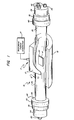
- a microwave deposition apparatus suitable for practicing the process of the present invention, is generally designated 10.
- the apparatus 10 comprises a tubular chamber or vessel 12 containing a substrate 14 upon which the amorphous semiconductor alloy films are to be deposited.
- the substrate may, but need not be heated by a radiant heater 16.
- the exterior of the chamber is irradiated by an energy source 17 to the plasma.
- Reaction gases passing from inlets 46 to an outlet 20 at opposite ends of the chamber 12 receive plasma igniting and maintaining energy, e.g., microwave energy, from the source 17 in the area of the substrate.
- the combination of the reaction gases and the energy from the source 17 causes the formation of the plasma and the deposit of the film 22 in the area of the substrate.
- the feedstock gases are substantially free of hydrogen compounds where hydrogen is bonded to another element, and include at least one multielement compound of an element to be deposited.
- the feedstock gas includes at least two components, one component being a halide of an element to be deposited, e.g., a fluoride or a chloride, and the other component including one or more elements, at least one element particularly adapted for scavenging the halogen, and at least one element forming the deposit, the two components being substantially free of hydrogen.
- the temperature of the substrate can be between room temperature and about 380 degrees Centigrade and the frequency of the microwave energy can be 2.45 Gigahertz and preferably above 2.45 Gigahertz.
- the combined plasma igniting and maintaining energy and the reaction gases form the plasma to permit the deposition process to proceed.
- the film 22 is spared from the potentially damaging effects of ion bombardment because of the reduced substrate self bias.
- the tubular chamber 12 comprises a central quartz portion 24 and end portions 26 at opposite ends thereof.
- the end portions 26 are closed by a pair of end fittings 30 and 32 to complete the chamber.
- Each of the end fittings includes a sleeve portion 34 extending from a closed end 36 to an open end portion.
- the open end portion is threaded to receive a collar 40 having an inwardly extending annular flange 42 at one end thereof.
- An o-ring (not shown) is confined in a space between the flange 42 and the end portion for compression thereof against the quartz portion 26.
- An air-tight seal is provided in this way between the end fittings 30 and 32 and the tubular chamber 12.
- the end fittings 30 and 32 are preferably made of stainless steel or other suitable non-corrosive metal, with the closed ends 36 being welded or otherwise permanently joined to the sleeve portions 34.
- the closed end 36 of the end fitting 32 is provided with gas inlets 46 through which the deposition gases are introduced into the vessel 12.
- An inert gas such as argon can be introduced through one inlet 46 to assist in sustaining the plasma.
- the gas inlets 46 are preferably connected to a conventional gas rack (not shown) for establishing regulated flows of feedstock gases therein.
- the outlet 20 is provided at the closed end 36 to the end fitting 30 for connection to selectable first and second pumps.
- the first pump provides for initial evacuation of the chamber.
- the second pump provides withdrawal of unused reaction gases during operation and maintenance of the proper deposition pressure of about 0.1 Torr or lower, e.g. 0.004 to 0.01 Torr.
- the energy source e.g., a microwave energy source 17, preferably comprises a microwave energy generator 18 coupled to an antenna 19.
- the antenna 19 is housed within a reflective housing 21 for concentration of the microwave energy into the chamber 12.
- the antenna as illustrated is a vertical antenna being preferably one-quarter wavelength long. The tip of the antenna just touches the outer surface of the vessel 12 to maximize transmission of its output to the reaction gases.
- Microwave excitation of a multicomponent, multielement feedstock gas forms a plasma that yields a hard, adherent deposit on a substrate 14 at temperatures as low as standard temperature (20-27 degrees Centigrade).
- a substrate may be heated if necessary, e.g., to control the morphology of the deposit. Heating may be done by radiant heater 16.
- the radiant heater 16 preferably comprises a conventional resistive heater. Heat is transmitted to the substrate 14 and the chamber 12 by radiation. Without significant direct heating of the reaction gases.
- a resistive heating arrangement may be provided within the chamber 12 for heating the substrate 14. In that case, power lines for the heating element would be passed through the closed end 36 of one of the end fittings.
- cooling can be supplied to the substrate 14 or substrate carrier to prevent thermal degradation of the substrate.
- the system 10 is first pumped down to below a desired deposition pressure such as 10 ⁇ 5 Torr.
- the feedstock gases i.e., a hydrogen free, multielement, multiatomic halide compound of the metal or semi-metal to be deposited, and a hydrogen free multiatomic molecular compound of the non-metal to be co-deposited therewith, and of the element to scavenge the halogen, are fed into the chamber 24.
- Exemplary are silicon tetrafluoride i.e., silane tetrafluoride, (SiF4), disilane hexafluoride (Si2F6), and higher homologues thereof; germane tetrafluoride, digermane hexafluoride, and higher homologues; boron trifluoride, BF3 and phosphorous trifluoride, PF3, with the N2, NH3, NO2, cyanogen [(CN)2], optimally with O2, and/or a fluorocarbon.
- SiF4 silane tetrafluoride
- Si2F6 disilane hexafluoride
- germane tetrafluoride digermane hexafluoride
- boron trifluoride BF3 and phosphorous trifluoride, PF3, with the N2, NH3, NO2, cyanogen [(CN)2], optimally with O2, and/or a fluorocarbon.
- the feedstock gases are fed into the inlet chamber 24 through inlet conduits, as separate inlet conduits 46 and chamber 12 is brought up to the desired operating pressure of, for example, about an order of magnitude below that of a comparable r.f., e.g., up to about 0.05 Torr.
- the precursor feed stock gas is a hydrogen free gas. That is, it is free of combined hydrogen, silanes, partially halogenated silanes, hydrocarbons, and partially substituted hydrocarbons, and contains only enough molecular hydrogen, H2 as may be necessary to control or modify the deposit properties. It is noted that the presence or degree of presence of H2 is optional and controllable.
- the microwave energy from the antenna 19 is directed by the reflective housing 21 into the vessel 12 to form a plasma in the area of the substrate.
- a film 22, such as a substantially optically transmissive, hard protective film 22 is deposited onto the substrate 14.
- the heater 16, when present, may maintain the substrate 14 at a temperature between about 20° Centigrade and a temperature below the onset of thermal degradation thereof.
- the use of a microwave excited per fluorosilane allows the substrate 14 to be at ambient temperature, obviating the necessity of a substrate heater.
- the output power of the microwave energy generator 18 is adjusted between about 20 and 120 watts depending on the volume of the gas contained in the plasma and the composition of the gas. These power outputs preferably correlate to about 0.1 to 1 watt per cubic centimeter in power density.
- the flow rate of the reaction gases can be between 1 to 50 SCCM. With the foregoing system parameters, deposition rates of 25A to 250A per second can be obtained.
- band gap increasing elements such as carbon or nitrogen can be incorporated into the films by introducing a halocarbon, nitrogen oxide, nitrogen halide, or other non-hydrogen containing gas into the vessel during deposition.
- the reaction gases can be sequentially introduced to result in the formation of any desired layer morphology, composition, or mechanical properties.
- a plasma sustaining gas can be introduced into one of the inlets 46.
- Argon gas can be utilized for this purpose.
- the method of the invention may be carried out with DC excited plasmas, and with AC excited plasmas, e.g., in the RF domain, the maximum benefits of the invention are obtained with a microwave maintained plasma.
- the deposition of substantially hydrogen free, hard alloy films by the foregoing inventive process utilizing a microwave initiated and maintained plasma has demonstrated many advantages over prior deposition processes. Firstly, the microwave energy provides a higher density of free radicals than previously possible. This results in higher deposition rates, nearly total utilization of the feed stock reaction gases. Secondly, the higher plasma electron temperature results in formation in the plasma of reactive species otherwise not obtainable and therefore one can deposit films containing unusual elements or combinations of elements or deposit films from unusual gas mixtures. This can result in new materials having unique compositional and structural properties.
- amorphous is meant an alloy or material which has long range disorder, although it may have short or intermediate order or even contain at times some crystalline inclusions. Pursuant to this definition, it should be noted that microcrystalline semiconductor alloy material will fall into the generic category of amorphous films.
- Figures 2 and 3 are side-by-side comparisons of the modified Paschen curve for SiH4. The curves are shown for SiH4 rather then for SiF4, because of the greater availability of data for SiH4, enabling SiH4 to be a standardized basis of comparison.
- FIGURE 2 illustrates a curve 260 which is produced utilizing conventional RF deposition techniques of SiH4, which is a modified Paschen curve.
- the Paschen curve shows the voltage needed to sustain a plasma as a function of pressure.
- the modified curve is related to the power needed to sustain a plasma as a function of pressure.
- the normal operating range is dictated by the minimum of the curve, which for the curve shown is about 0.2 to 0.25 Torr.
- FIGURE 3 illustrates a modified Paschen curve 262 for the microwave deposition process of the invention again utilizing SiH4 as the reaction gas.
- the curve 262 shows the clear shift in the curve to lower pressure for the microwave deposition process of the invention, which results in an operating range of about 0.075 to 0.1 Torr or below for the invention.
- the curve shifts for other reaction gases and deposition system dimensions.
- the hard, optically transparent, protective layer is characterized by an optical absorption through a 3 micron film of less than ten percent at a relevant bandwidth.
- the relevant bandwidth may be the visible spectrum (600 nanometers to 400 nanometers) or the infrared spectrum (longer than 600 nanometers and even longer than 700 nanometers). This requires an optical bandgap of greater than 3.5 electron volts for transmission in the visible spectrum, and greater than 2.5 electron volts for transmission in the infrared spectrum.
- Exemplary, transparent, low cost, hard, abrasion resistant materials include the silicon compounds, especially the silicon carbides, SiCx with x from 0 to 2.0, the silicon nitrides SiN y where y is from 0 to 4/3, the silicon oxides, SiO z , where z is from 0 to 2, and related compositions as SiC x O z , SiC x N y , SiN y O z , and SiC x N y O z , where x, y, and z are as defined above, and the sum of x/2 plus 3y/y plus z/2 approaches 1.00.
- Illustative materials are:
- the above described coatings may be deposited directly on the substrate.
- an inner layer or underlayer may be deposited directly on the substrate, with the above described hard coating deposited atop the inner layer or underlayer.
- the inner layer or underlayer may serve as a stress relieving layer, allowing bending of the laminate and reducing the tendency for stress cracking in the dielectric layer. This allows a thicker layer to be deposited.
- This also allows a flat substrate as a thermoplastic film or sheet to be coated with the inner layer and the external hard layer and thereafter shaped or formed, i.e., bent, molded, extruded, drawn, oriented, or otherwise thermoformed, without cracking, crazing, hazing, or delumination.
- the coating may be deposited on a large flexible plastic substrate at one site or factory in one apparatus by one manufacturing enterprise, and the coated plastic substrate shaped or formed in another apparatus, or at a different site or factory, and even by a different manufacturing enterprise.
- the underlayer or inner layer may also act as an optical filter, being of controlled band gap, so as to selectively block portions of the spectrum, as ultraviolet and/or blue light.
- the inner layer when present, should be formed of a material that is compatible with the substrate in one or more of coefficient of thermal expansion, modulus of elasticity, plasticity, or lattice dimensions.
- the inner layer is deposited carbon.
- the deposited carbon may be amorphous, microcrystalline, or polycrystalline, and may exhibit tetrahedral short range order and/or graphitic short range order.
- the carbon may be deposited by sputtering a carbon target, chemical vapor deposition, glow discharge from a halocarbon feedstock gas, or microwave deposition fro a halocarbon feedstock gas.
- the inner layer of the dielectric is formed of an alloy hydrogen and the same constituents as the outer portion of dielectric.
- the hydrogen content of the inner layer of the dielectric is controlled by introducing a separate hydrogen containing feedstock gas, as a hydride, e.g., silane or germane, or molecular hydrogen.
- a separate hydrogen containing feedstock gas as a hydride, e.g., silane or germane, or molecular hydrogen.
- a separate hydrogen containing feedstock gas as a hydride, e.g., silane or germane, or molecular hydrogen.
- the deposition rate and substrate temperature are controlled independently of the hydrogen feed rate, it is possible to incorporate hydrogen at a concentration that will relieve stresses within the dielectric layer, thereby reducing hazing, crazing, and delamination.
- the inner layer whether a carbonaceous under layer or hydrogen alloy inner layer, may be of uniform composition and properties or of graded composition and properties.
- the inner layer when present, has a thickness of from about 0.05 micron (500 Angstroms) to about 2 micron, with a thickness of about 0.1 micron to 1.5 micron being particularly preferred for stress relieving SiO2 alloys on polycarbonates and polymers of like mechanical and thermal properties.
- the coating may contain a gas-impervious intermediate layer, as a Si3N4 layer, to hermetically seal an environmentally degradable substrate, as polycarbonate, or polyurethane, from oxygen and/or water vapor, an outer layer of, e.g., SiO2, for hardness, and an adhesion layer or layers, e.g., of C or SiO2, or both C and SiO2 for adhesion, bonding, and mechanical parameter matching.
- a gas-impervious intermediate layer as a Si3N4 layer
- an environmentally degradable substrate as polycarbonate, or polyurethane
- an outer layer e.g., SiO2 for hardness
- an adhesion layer or layers e.g., of C or SiO2, or both C and SiO2 for adhesion, bonding, and mechanical parameter matching.
- a polycarbonate or polyurethane substrate may have a hard coating and be protected from moisture and/or O2 by a multilayer coating of (1) SiO2, e.g., as an adhesion layer, (2) Si3N4, e.g., as a hermetic seal layer, and (3) SiO2, e.g. as a hard outer layer.
- the SiO2 layers have a thickness of about 1 to 2.5 microns, and the Si3N4 layer has a thickness sufficient to substantially prevent the permeation of gas, as O2 or H2O, therethrough, e.g, about 0.5 micron to 2 microns thick.
- a carbon film may be deposited on the substrate, and the layers of SiO2 and Si3N4 deposited sequentially, e.g., as described above, atop the carbon layer.
- SiO2 and Si3N4 deposited sequentially, e.g., as described above, atop the carbon layer.
- a multilayer coating may be deposited having an inorganic photochromic or electrochromic composition, as a hexa-coordinated tungsten composition, encapsulated between hermetically sealing layers of silicon nitride, with an external layer of silicon oxide.
- the photochromic may be deposited by low temperature CVD, from organic solution or by condensation from an organic vapor, as is well known in the art.
- This multilayer coating may be deposited atop, e.g., a poly(acrylic), poly(carbonate), or poly(allyl glycol carbonate) homopolymer, copolymer, or interpolymer substrate, optionally with a carbonaceous and/or silicon oxide containing bottom layer, a first silicon nitride encapsulating layer, the photochromic or electrochromic layer, a second silicon nitride encapsulating layer, and an external layer of silicon dioxide.
- the first silicon oxide layer may be dispensed with and the photochromic or electrochromic layer deposited onto the silicon oxide and/or carbon containing under layer, or even directly onto the organic polymeric substrate.
- Microwave plasma deposited protective, optically transmitting layers meeting these criteria find utility in combination with optically transmissive organic polymeric substrates.
- Exemplary polyolefins include polyethylene, polyethylene-polyvinyl acetate copolymers, polyethylene-polyethyl acrylate copolymers, polyethylene-polyacrylic acid copolymers, polypropylene - polymethacrylic acid copolymers, polypropylene, polyethylene-polypropylene copolymers, polyethylene-polypropylene-polydiene terpolymers, chlorinated polyethylene, chlorosulfonated polyethylene, polyisobutylene-polyisoprene copolymers, and poly 4-methyl pentene-1.
- Exemplary aromatic carbon chain polymers include polystyrene, polystyrene-acrylonitrile copolymers, polystyrene-polybutadiene copolymers, polystyrene-divinylbenzene copolymers and terpolymers and polystyrene-polyester copolymers.
- Exemplary diene polymers include polybutadiene, polybutadiene-polyacrylonitrile copolymers, polyisoprene, polychloroprene, polyisoprene-polystyrene copolymers, and polyisoprene-polymethyl methacrylate copolymers.
- Exemplary vinyl polymers include polyvinyl chloride, polyvinylidene chloride, polyvinyl chloride - polyvinylidene chloride copolymers, polyvinyl chloride-polyvinylidene chloride, polyvinyl chloride-polyethylene, polyvinyl acetate, polyvinyl chloride - polyvinyl acetate, hydrolyzed polyvinyl acetate, also known as polyvinyl alcohol, poly N-vinyl pyrrolidone, poly 2-vinyl pyridene, poly vinyl-methyl ether, poly vinyl formal, poly vinyl butyral, and poly acrylic acid-polyethylene copolymers.
- Exemplary acrylic polymers include polymethacrylic acid, polyethyl acrylate, polymethylmenacrylate, polyethyl acrylate - poly methyl melhacrylate copolymers, poly methyl methacrylate - polystyrene copolymers, and polyacrylamides.
- Exemplary fluorocarbons include polyvinyl fluoride, poly tetrafluoroethylene, polychlorotrifluoroethylene, polyperfluoropropylene, polyvinylidene fluoride, polyperfluoropropylene - polytetrafluoroethylene copolymers, polyperfluoropropylene-polyvinylidene fluoride copolymers, and polyvinylidene fluoride - poly chlorotrifluoroethylene copolymers.
- the above enumeration is intended to be illustrative and not exclusive and the useful polymers include various analogs, homologs, and adducts thereof.
- Especially preferred carbon chain polymers include high density, crystalline polyolefins, with a molecular weight above about 100,000
- the method of this invention is also useful in providing hard coatings on substrates of heterochain polymers such as polyesters, polyethers, polyamides and polyimides, polyols, polyurethanes, and polysilicones.
- exemplary polyesters include alkyds (as alkyd films having the herein contemplated and described dielectric coatings therein), gylcol-maleic acid anhydride ester polymers, glycol-allyl carbonate polymers (as allyl glycol carbonate polymers, exemplified by diethylene glycol bis(allyl carbonate)), saturated ester polyesters as terephthelate polyesters, and polycarbonates (e.g.
- polyethers include polyacetal, polyalkylene oxides (as polyethylene oxides, polypropylene oxides, and polyepichlorohydrin), urethane-polyol copolymers, polytetrahydrofuran, polyphenylene oxides, and polysulfones.
- exemplary useful polyamides and polyimides include nylons, "dimer acids", aryl nylons, the polymeric reaction products of, e.g., 4-4 ⁇ -Diaminophenyloxide and pyromellitic dianhydride, and the polymeric reaction products of diphenylisophthalates.
- Exemplary polyals include the melamines.
- Exemplary useful polyurethanes include those used to form elastomers (as cast and thermoplastic polyurethanes) by the reaction of a diisocyanate, methylene-bis (4) phenyl isocyanite, or hexamethylene diisocyanate, optionally with a chain extending agent, and a diol, as a polyester diol.
- the above enumeration of heters chain polymers is intended to be illustrative and not exclusive or limiting.
- the monomers may be homopolymers or copolymers, as terpolymers.
- the copolymers may be random copolymers or block copolymers.
- the organic polymeric substrate is generally substantially cured prior to deposition of the transparent, multielement alloy film
- the organic polymer may be partially polymerized, i.e., still containing monomeric bonds, e.g., gummy and viscous, or even having liquid portions, and may contain a photoinitiatar or photocatalyst, which completes the polymerization or cure during the glow discharge deposition of the multielement alloy.
- the organic polymeric substrate may contain a partially polymerized vinyl or acrylic material and an optical radiation or ultra violet initiated catalyst, as riboflavin-S-phosphate and sodium, which is initiated by the optical or U.V. radiation from the plasma, to increase the degree of polymerization and further bond the multiple element alloy to the organic polymeric substrate.
- FIGURE 4 shows an optical data storage device 310 as disk 310.
- the disk 310 includes a grooved substrate 320, carrying a data storage medium 330, and overlaid with a plastic protective overlay 340.
- Information is stored in the data storage medium by changing the state thereof, e.g., the microstructure, the surface morphology, the reflectivity, the presence or absence of bubbles or hollows, or ablation of the medium.
- the individual memory cells of the disk 310 are small, on the order of 0.1 to 2.0 microns. As a result, any scratches, pits, gauges, imperfections, dust, or the like in the plastic overlay 340 can give rise to improper readings, skips, or the like. However, these defects in the optical path through the plastic overlay 340 are substantially reduced by the hard, optically transmissive protective layer 350.
- FIGURE 5 shows an opthalmic lens 401 having a plastic substrate 411 with the herein contemplated hard coating 420 therein.
- the plastic substrate may be a polycarbonate a polyacrylate, such as poly(methyl methacrylate) or a poly(allyl carbonate) such as PPG Industries "CR-39” (R) diethylene glycol bis (allyl carbonate), polymerized with a suitable peroxide initiator to form a hard, substantially light transmissive polymer.
- the coating 420 is generally from about 1 to about 10 microns thick and particularly from about 2 to about 5 microns thick. It may be a graded coating, with a carbon underlayer, as a vacuum deposited carbon coating, film, or layer of 0.5 to 2.0 micron thickness, and of graphitic or partially graphitic structure, and a silicon alloy layer atop the carbon layer.
- the silicon containing alloy layer may be comprised of: silicon dioxide, silicon carbide, silicon nitride, silicon carboxynitride, or other microwave deposited, transparent silicon alloy hard coating.
- the coating 420 may be of narrow optical band gap so as to block and/or reflect certain optical band widths, i.e., as an optical filter.
- the coating is a multilayer coating with a deposited carbon underlayer on the plastic substrate 411.
- the carbon e.g., the deposited amorphous, graphitic or tetrahedrally coordinated material may have an optical band gap to selectively absorb blue and ultraviolet.
- the plastic substrate could also be a plastic optical fiber, or laser mirror, or a plastic sheet, as a door, window, sun roof insert, or the like.
- the coated article may be a glass-plastic laminate having the contemplated hard coating on the surface of the plastic unprotected from the glass.
- exemplary is a windshield 501 as shown in Figures 6 and 7.
- the article could be a window, a storm door glazing unit, or a sliding door glazing unit.
- the windshield 501 includes a glass substrate 521 with a thin adhesive layer 523 of, for example, polyvinyl alcohol, and a plastic film 525, for example a substantially water white polyurethane.
- the hard coating for example the silicon carbide, silicon nitride, or silicon oxide hard coating 531 is on the unprotected surface of the plastic layer 525. This results in a significant reduction in abrasion and scratching of the plastic 525.
- FIG. 8 An alternative exemplification is shown in Figure 8.
- the exemplification shown in Figure 8 is a plastic sheet 601 having the hard coating 635 on at least the surface exposed to abrasion.
- hard coatings 635 may be on both surfaces of the plastic sheet 601. In this way both the weather incident surface and the interior surface have abrasion resistant coatings.
- FIG. 9 A still further exemplification is shown in Figure 9 where a plastic head light lens 701 is shown.
- the plastic head light lens 701 has a plastic substrate, as an injection molded plastic substrate 701, with a thin film of the herein contemplated hard coating deposited thereon.
- the film is used as a passivation layer for an electronic device or as an interlevel insulator gate dielectric for a MOSFET, such as a Si3N4 or SiO2 thin film, and especially on Si3N4 film, optionally containing fluorine.
- the dielectric is deposited at a low device temperature, that is, at a temperature low enough to avoid diffusion of sharp profiles of ion implanted dopants across.
- a feedstock gas of a halocarbon as CF4 or C2F6, boron trifluoride, and a nitrogen source, as N2 or cyanogen (CN)2
- a precursor gas that deposits to form a disordered boron-carbon coating can be decomposed by microwave energy to form a precursor gas that deposits to form a disordered boron-carbon coating.
- the disordered boron-carbon composition which may have proportions approaching B4C, is a hard material useful as, for example, a wear coating, as on razor blades, scissors, cutlery, cutting tools, and the like.
- a disordered B4C coating of about 0.5 to 5 microns thick is applied to a cutting surface, as a scissor, razor blade, or knife, by the microwave plasma decomposition of a feedstock gas of (1) at least one alocarbon chosen from CF4, C2F6, and volatile homologous thereof; (2) BF3, and (3) a nitrogen source as N2 or (CN)2.
- An NF3 gas is recovered during the deposition.
- a photovoltaic cell formed of a plurality of successively deposited n-i-p layers, each of which comprises a substantially amorphous thin film semiconductor alloy material is shown generally by the reference numeral 810.
- Figure 10 shows a tandem n-i-p type photovoltaic device, such as a solar cell, made up of individual n-i-p type cells 812 a , 812 b and 812 c .
- a substrate 11 which may be formed of a transparent glass or synthetic polymeric member; or formed from a metallic material such as stainless steel, aluminum, tantalum, molybdenum, chrome; or formed from metallic particles embedded within an insulator.
- the term "substrate” shall include not only a flexible film, but also any elements added thereto by preliminary processing.
- Each of the cells 812 a , 812 b and 812 c are preferably fabricated with a thin film semiconductor body containing at least a silicon or silicon:germanium alloy.
- Each of the semiconductor bodies includes a p-type conductivity semiconductor layer 820 a , 820 b and 820 c ; a substantially intrinsic semiconductor layer 818 a , 818 b and 818 c ; and an n-type conductivity semiconductor layer 816 a , 816 b and 816 c .
- the intrinsic layer may include traces of n-type or p-type dopant material without forfeiting its characteristic neutrality, hence it may be referred to herein as a "substantially intrinsic layer".
- cell 812 b is an intermediate cell and, as indicated in Figure 13, additional intermediate cells may be stacked atop the illustrated cells without departing from the spirit or scope of the present invention.
- the tandem cell may include only two stacked cells.
- n-i-p photovoltaic cells are illustrated, this invention may be advantageously practiced with differently configured photovoltaic cells including single or multiple p-i-n cells, Schottky barrier cells, p-n cells as well as with any other semiconductor device having an appropriate top electrode.
- n-i-p type as used herein is meant to include any aggregation of n, i and p layers operatively disposed to provide a photoactive region for generating charge carriers in response to the absorption of photon energy.
- a further deposition process may be either performed in a separate environment or as a part of a continuous process.
- a TCO (transparent conductive oxide) layer 822 preferably formed of a material such as tin oxide, indium oxide, indium tin oxide, zinc oxide, cadmium stannate or combinations thereof is added atop the p-layer 820 c of the top most cell 812 c , to function as the top electrode of the cell 10.
- An electrode grid 824 may be added to the device where the cell is of a sufficiently large area, or if the conductivity of the TCO layer 822 is insufficient to obtain efficient collection of photogenerated current.
- the grid 824 is adapted to shorten the carrier path and increase the conduction efficiency.
- the intrinsic layers 818 a , 818 b and 818 c of the cells 812 a , 812 b and 812 c may be and preferably are formed from semiconductor alloy materials having different bandgaps.
- intrinsic layer 818 c of cell 812 c may have a band gap of approximately 1.7 eV
- intrinsic layer 818 b of cell 812 b may have a band gap of approximately 1.5 eV
- intrinsic layer 818 a of cell 812 a may have a band gap of approximately 1.3 eV. In this manner, the most efficient use may be made of a large portion of the incident solar spectrum.
- a solar cell shown generally as 810, included a layer of about 18 mil thick transparent flowable organic resin (such as EVA (ethyl vinyl acetate)), generally 826 in Figure 10, which resin would adhere to the subjacent transparent conductive oxide 822 and grid structure 824 as well as provide for step coverage of that non-planar grid structure.
- EVA ethyl vinyl acetate
- the EVA by itself is characterized by excellent weatherability and no UV absorbtions.
- an outer layer of about a 2-4 mil thick, relatively hard, transparent laminate, generally 828 provided the outer environmental protection covering.
- An example of such a laminate was TEDLAR (registered trademark of Dupont Corporation).
- FEP fluorinated-ethylene-propylene
- FEP fluorinated-ethylene-propylene
- transparent laminates such as FEP with a hard, protective, abrasion resistant, hermetic overcoat, shown generally as 830 in Figure 10.
- the wide bandgap silicon oxi-nitrides, silicon oxides or silicon carbides discussed hereinabove provide a hard, transparent, flexible, adherent laminate. It is further possible to deposit said hard coatings directly upon the flowable organic resin (such as EVA) 826 or, where step coverage is not a problem, directly upon the TCO layer 822.
- EVA flowable organic resin
- a series of polycarbonate substrate coupons were coated with alloy hard coatings.
- a coupon was placed in a vacuum vessel coupled to a source of 2.45 Gigahertz microwave energy.
- the vacuum vessel was sealed, purged with argon, and pumped down.
- a feedstock gas mixture was introduced in the vacuum vessel, the microwave energy source energized to initiate and maintain a plasma, and the pressure is adjusted and maintained at 3.5 millitorr.
- the feedstock gas had the composition shown in column 1 (atomic %).
- the substrate temperature is shown in column 2.
- the resulting coating had the thickness shown in column 3, and the composition (atomic %) shown in column 5.
Landscapes
- Chemical & Material Sciences (AREA)
- Engineering & Computer Science (AREA)
- Physics & Mathematics (AREA)
- Plasma & Fusion (AREA)
- Analytical Chemistry (AREA)
- Materials Engineering (AREA)
- Chemical Kinetics & Catalysis (AREA)
- Mechanical Engineering (AREA)
- Metallurgy (AREA)
- Organic Chemistry (AREA)
- General Chemical & Material Sciences (AREA)
- Inorganic Chemistry (AREA)
- Chemical Vapour Deposition (AREA)
- Secondary Cells (AREA)
- Battery Electrode And Active Subsutance (AREA)
Applications Claiming Priority (2)
| Application Number | Priority Date | Filing Date | Title |
|---|---|---|---|
| US07/032,263 US4737379A (en) | 1982-09-24 | 1987-03-31 | Plasma deposited coatings, and low temperature plasma method of making same |
| US32263 | 1996-12-03 |
Publications (3)
| Publication Number | Publication Date |
|---|---|
| EP0284693A2 true EP0284693A2 (de) | 1988-10-05 |
| EP0284693A3 EP0284693A3 (en) | 1989-03-22 |
| EP0284693B1 EP0284693B1 (de) | 1994-08-31 |
Family
ID=21863988
Family Applications (1)
| Application Number | Title | Priority Date | Filing Date |
|---|---|---|---|
| EP87310966A Expired - Lifetime EP0284693B1 (de) | 1987-03-31 | 1987-12-14 | Plasmaverfahren zur Herstellung mittels einer Plasmaentladung hergestellter Schichten bei niedriger Temperatur |
Country Status (6)
| Country | Link |
|---|---|
| US (1) | US4737379A (de) |
| EP (1) | EP0284693B1 (de) |
| JP (1) | JP2648492B2 (de) |
| AT (1) | ATE110795T1 (de) |
| CA (1) | CA1325793C (de) |
| DE (1) | DE3750470T2 (de) |
Cited By (3)
| Publication number | Priority date | Publication date | Assignee | Title |
|---|---|---|---|---|
| EP0502790A1 (de) * | 1991-03-06 | 1992-09-09 | L'air Liquide, Societe Anonyme Pour L'etude Et L'exploitation Des Procedes Georges Claude | Mehrlagiger Überzug für ein Polycarbonatsubstrat |
| GB2325938A (en) * | 1997-06-03 | 1998-12-09 | Nec Corp | Method of forming a fluorine containing insulating film |
| EP0992610A3 (de) * | 1998-09-30 | 2003-10-15 | Becton Dickinson and Company | Sperrschicht auf Kunststoff-Substraten und Verfahren zu ihrer Herstellung |
Families Citing this family (188)
| Publication number | Priority date | Publication date | Assignee | Title |
|---|---|---|---|---|
| JPH0676666B2 (ja) * | 1987-02-10 | 1994-09-28 | 株式会社半導体エネルギ−研究所 | 炭素膜作製方法 |
| US4912065A (en) * | 1987-05-28 | 1990-03-27 | Matsushita Electric Industrial Co., Ltd. | Plasma doping method |
| DE3725700A1 (de) * | 1987-08-03 | 1989-02-16 | Siemens Ag | Neues halbleitergrundmaterial |
| US4973345A (en) * | 1987-10-13 | 1990-11-27 | British Telecommunications Public Limited Company | Surface treatments for optical fibre preforms |
| USH665H (en) | 1987-10-19 | 1989-08-01 | Bell Telephone Laboratories, Incorporated | Resistive field shields for high voltage devices |
| US5424131A (en) * | 1987-11-30 | 1995-06-13 | Polyplasma, Inc. | Barrier coatings on spacecraft materials |
| US5041303A (en) * | 1988-03-07 | 1991-08-20 | Polyplasma Incorporated | Process for modifying large polymeric surfaces |
| US4822703A (en) * | 1988-04-04 | 1989-04-18 | Xerox Corporation | Photoresponsive imaging members with polygermanes |
| NL8801379A (nl) * | 1988-05-30 | 1989-12-18 | Imec Inter Uni Micro Electr | Werkwijze voor het vervaardigen van een dunne-filmtransistor en een dergelijke dunne-filmtransistor. |
| DE3923390A1 (de) * | 1988-07-14 | 1990-01-25 | Canon Kk | Vorrichtung zur bildung eines grossflaechigen aufgedampften films unter verwendung von wenigstens zwei getrennt gebildeten aktivierten gasen |
| JPH02159716A (ja) * | 1988-12-14 | 1990-06-19 | Shin Etsu Chem Co Ltd | X線リソグラフィー用SiC膜およびその成膜方法 |
| AU624203B2 (en) * | 1988-12-21 | 1992-06-04 | Sumitomo Electric Industries, Ltd. | Method and apparatus for producing coated optical fiber |
| US5227196A (en) * | 1989-02-16 | 1993-07-13 | Semiconductor Energy Laboratory Co., Ltd. | Method of forming a carbon film on a substrate made of an oxide material |
| JP3111353B2 (ja) * | 1989-08-31 | 2000-11-20 | 橋本フォーミング工業株式会社 | 透明樹脂成形品の製造方法 |
| US5190792A (en) * | 1989-09-27 | 1993-03-02 | International Business Machines Corporation | High-throughput, low-temperature process for depositing oxides |
| US5198298A (en) * | 1989-10-24 | 1993-03-30 | Advanced Micro Devices, Inc. | Etch stop layer using polymers |
| JPH03144938A (ja) * | 1989-10-30 | 1991-06-20 | Sharp Corp | 光メモリ素子 |
| US5229165A (en) * | 1989-11-09 | 1993-07-20 | Allied-Signal Inc. | Plasma sprayed continuously reinforced aluminum base composites |
| US4981713A (en) * | 1990-02-14 | 1991-01-01 | E. I. Du Pont De Nemours And Company | Low temperature plasma technology for corrosion protection of steel |
| FR2661688B1 (fr) * | 1990-05-02 | 1992-07-17 | Air Liquide | Revetement multicouche pour substrat polycarbonate et procede d'elaboration d'un tel revetement. |
| JP3090979B2 (ja) * | 1990-09-04 | 2000-09-25 | 株式会社リコー | 基板付薄膜積層デバイスおよびその製法 |
| EP0478233B1 (de) * | 1990-09-27 | 1996-01-03 | AT&T Corp. | Verfahren zur Herstellung integrierter Schaltungen |
| US5234748A (en) * | 1991-06-19 | 1993-08-10 | Ford Motor Company | Anti-reflective transparent coating with gradient zone |
| US5231048A (en) * | 1991-12-23 | 1993-07-27 | United Solar Systems Corporation | Microwave energized deposition process wherein the deposition is carried out at a pressure less than the pressure of the minimum point on the deposition system's paschen curve |
| JPH0697070A (ja) * | 1992-09-11 | 1994-04-08 | Sanyo Electric Co Ltd | 多結晶シリコン膜の製造方法 |
| US5670224A (en) * | 1992-11-13 | 1997-09-23 | Energy Conversion Devices, Inc. | Modified silicon oxide barrier coatings produced by microwave CVD deposition on polymeric substrates |
| JP2804700B2 (ja) * | 1993-03-31 | 1998-09-30 | 富士通株式会社 | 半導体装置の製造装置及び半導体装置の製造方法 |
| US20040241454A1 (en) * | 1993-10-04 | 2004-12-02 | Shaw David G. | Barrier sheet and method of making same |
| US5565248A (en) * | 1994-02-09 | 1996-10-15 | The Coca-Cola Company | Method and apparatus for coating hollow containers through plasma-assisted deposition of an inorganic substance |
| US6149982A (en) * | 1994-02-16 | 2000-11-21 | The Coca-Cola Company | Method of forming a coating on an inner surface |
| ES2131810T5 (es) * | 1994-02-16 | 2004-02-16 | The Coca-Cola Company | Recipientes huecos con superficies interiores inertes o impermeables producidas por reaccion superficial asistida por plasma o polimerizacion sobre la superficie. |
| US5571470A (en) * | 1994-02-18 | 1996-11-05 | The Coca-Cola Company | Method for fabricating a thin inner barrier layer within a preform |
| JP3061255B2 (ja) * | 1995-08-18 | 2000-07-10 | キヤノン販売株式会社 | 成膜方法 |
| US6316111B1 (en) * | 1996-03-01 | 2001-11-13 | Cardinal Cg Company | Heat-emperable coated glass article |
| US6231999B1 (en) * | 1996-06-21 | 2001-05-15 | Cardinal Ig Company | Heat temperable transparent coated glass article |
| US6627305B1 (en) * | 1997-07-16 | 2003-09-30 | Koninklijke Philips Electronics N.V. | Substrates for large area electronic devices |
| US5959247A (en) * | 1997-07-22 | 1999-09-28 | Armstrong; Joseph H. | Low cost protective coating and method for a die-on-board electronic assembly |
| US6090358A (en) * | 1997-08-20 | 2000-07-18 | National Science Council Of Republic Of China | Crystalline Six Cy Nz and method for synthesis |
| DE19744060C2 (de) * | 1997-10-06 | 1999-08-12 | Fraunhofer Ges Forschung | Verfahren und Vorrichtung zur Oberflächenbehandlung von Substraten |
| US6051321A (en) | 1997-10-24 | 2000-04-18 | Quester Technology, Inc. | Low dielectric constant materials and method |
| US6020458A (en) | 1997-10-24 | 2000-02-01 | Quester Technology, Inc. | Precursors for making low dielectric constant materials with improved thermal stability |
| US6287888B1 (en) | 1997-12-26 | 2001-09-11 | Semiconductor Energy Laboratory Co., Ltd. | Photoelectric conversion device and process for producing photoelectric conversion device |
| JPH11279773A (ja) * | 1998-03-27 | 1999-10-12 | Tomoo Ueno | 成膜方法 |
| JP2002514004A (ja) | 1998-05-01 | 2002-05-14 | セシュー ビー デス | 化学蒸着によって堆積された酸化物/有機ポリマー多層薄膜 |
| JP4174862B2 (ja) * | 1998-08-04 | 2008-11-05 | ソニー株式会社 | 薄膜トランジスタの製造方法および半導体装置の製造方法 |
| US6140187A (en) * | 1998-12-02 | 2000-10-31 | Lucent Technologies Inc. | Process for forming metal oxide semiconductors including an in situ furnace gate stack with varying silicon nitride deposition rate |
| US6495208B1 (en) | 1999-09-09 | 2002-12-17 | Virginia Tech Intellectual Properties, Inc. | Near-room temperature CVD synthesis of organic polymer/oxide dielectric nanocomposites |
| JP3477148B2 (ja) * | 1999-12-02 | 2003-12-10 | カーディナル・シージー・カンパニー | 耐曇り性透明フィルム積層体 |
| EP1754691B1 (de) | 1999-12-02 | 2009-02-11 | Cardinal CG Company | Gegen Anlaufen beständiges durchsichtiges Beschichtungssystem |
| US6630413B2 (en) | 2000-04-28 | 2003-10-07 | Asm Japan K.K. | CVD syntheses of silicon nitride materials |
| US6559026B1 (en) | 2000-05-25 | 2003-05-06 | Applied Materials, Inc | Trench fill with HDP-CVD process including coupled high power density plasma deposition |
| US6193379B1 (en) | 2000-06-09 | 2001-02-27 | Gentex Corporation | Electrochromic assembly including at least one polymeric substrate |
| KR100797385B1 (ko) * | 2000-10-19 | 2008-01-24 | 로베르트 보쉬 게엠베하 | 유도 결합 플라즈마를 이용한 기판의 에칭 장치 및 방법 |
| US6638820B2 (en) | 2001-02-08 | 2003-10-28 | Micron Technology, Inc. | Method of forming chalcogenide comprising devices, method of precluding diffusion of a metal into adjacent chalcogenide material, and chalcogenide comprising devices |
| KR101027485B1 (ko) | 2001-02-12 | 2011-04-06 | 에이에스엠 아메리카, 인코포레이티드 | 반도체 박막 증착을 위한 개선된 공정 |
| JP4742429B2 (ja) * | 2001-02-19 | 2011-08-10 | 住友電気工業株式会社 | ガラス微粒子堆積体の製造方法 |
| US6727192B2 (en) | 2001-03-01 | 2004-04-27 | Micron Technology, Inc. | Methods of metal doping a chalcogenide material |
| US6734455B2 (en) * | 2001-03-15 | 2004-05-11 | Micron Technology, Inc. | Agglomeration elimination for metal sputter deposition of chalcogenides |
| US6896968B2 (en) * | 2001-04-06 | 2005-05-24 | Honeywell International Inc. | Coatings and method for protecting carbon-containing components from oxidation |
| US6732551B2 (en) | 2001-05-04 | 2004-05-11 | Corning Incorporated | Method and feedstock for making silica |
| US6740601B2 (en) | 2001-05-11 | 2004-05-25 | Applied Materials Inc. | HDP-CVD deposition process for filling high aspect ratio gaps |
| US7102150B2 (en) * | 2001-05-11 | 2006-09-05 | Harshfield Steven T | PCRAM memory cell and method of making same |
| US6596653B2 (en) * | 2001-05-11 | 2003-07-22 | Applied Materials, Inc. | Hydrogen assisted undoped silicon oxide deposition process for HDP-CVD |
| US6951805B2 (en) * | 2001-08-01 | 2005-10-04 | Micron Technology, Inc. | Method of forming integrated circuitry, method of forming memory circuitry, and method of forming random access memory circuitry |
| US6737312B2 (en) | 2001-08-27 | 2004-05-18 | Micron Technology, Inc. | Method of fabricating dual PCRAM cells sharing a common electrode |
| US6784018B2 (en) * | 2001-08-29 | 2004-08-31 | Micron Technology, Inc. | Method of forming chalcogenide comprising devices and method of forming a programmable memory cell of memory circuitry |
| US6955940B2 (en) * | 2001-08-29 | 2005-10-18 | Micron Technology, Inc. | Method of forming chalcogenide comprising devices |
| US6881623B2 (en) * | 2001-08-29 | 2005-04-19 | Micron Technology, Inc. | Method of forming chalcogenide comprising devices, method of forming a programmable memory cell of memory circuitry, and a chalcogenide comprising device |
| US6709958B2 (en) * | 2001-08-30 | 2004-03-23 | Micron Technology, Inc. | Integrated circuit device and fabrication using metal-doped chalcogenide materials |
| US20030047765A1 (en) * | 2001-08-30 | 2003-03-13 | Campbell Kristy A. | Stoichiometry for chalcogenide glasses useful for memory devices and method of formation |
| US6709714B2 (en) * | 2001-10-23 | 2004-03-23 | Tien Tsai Lin | Method and apparatus of producing high-density polyidimide (HPI) film |
| US6987162B2 (en) | 2001-10-23 | 2006-01-17 | Tien Tsai Lin | Method and apparatus of producing high-density polyimide (HPI) film |
| US6815818B2 (en) * | 2001-11-19 | 2004-11-09 | Micron Technology, Inc. | Electrode structure for use in an integrated circuit |
| US6791859B2 (en) * | 2001-11-20 | 2004-09-14 | Micron Technology, Inc. | Complementary bit PCRAM sense amplifier and method of operation |
| US6873538B2 (en) * | 2001-12-20 | 2005-03-29 | Micron Technology, Inc. | Programmable conductor random access memory and a method for writing thereto |
| US6909656B2 (en) * | 2002-01-04 | 2005-06-21 | Micron Technology, Inc. | PCRAM rewrite prevention |
| US20030143782A1 (en) * | 2002-01-31 | 2003-07-31 | Gilton Terry L. | Methods of forming germanium selenide comprising devices and methods of forming silver selenide comprising structures |
| US6867064B2 (en) * | 2002-02-15 | 2005-03-15 | Micron Technology, Inc. | Method to alter chalcogenide glass for improved switching characteristics |
| US6791885B2 (en) * | 2002-02-19 | 2004-09-14 | Micron Technology, Inc. | Programmable conductor random access memory and method for sensing same |
| US7087919B2 (en) * | 2002-02-20 | 2006-08-08 | Micron Technology, Inc. | Layered resistance variable memory device and method of fabrication |
| US6891749B2 (en) * | 2002-02-20 | 2005-05-10 | Micron Technology, Inc. | Resistance variable ‘on ’ memory |
| US7151273B2 (en) * | 2002-02-20 | 2006-12-19 | Micron Technology, Inc. | Silver-selenide/chalcogenide glass stack for resistance variable memory |
| US6809362B2 (en) * | 2002-02-20 | 2004-10-26 | Micron Technology, Inc. | Multiple data state memory cell |
| US6919133B2 (en) | 2002-03-01 | 2005-07-19 | Cardinal Cg Company | Thin film coating having transparent base layer |
| AU2003217818A1 (en) * | 2002-03-01 | 2003-09-16 | Cardinal Cg Company | Thin film coating having transparent base layer |
| US6937528B2 (en) * | 2002-03-05 | 2005-08-30 | Micron Technology, Inc. | Variable resistance memory and method for sensing same |
| US6849868B2 (en) * | 2002-03-14 | 2005-02-01 | Micron Technology, Inc. | Methods and apparatus for resistance variable material cells |
| US6858482B2 (en) * | 2002-04-10 | 2005-02-22 | Micron Technology, Inc. | Method of manufacture of programmable switching circuits and memory cells employing a glass layer |
| US6864500B2 (en) * | 2002-04-10 | 2005-03-08 | Micron Technology, Inc. | Programmable conductor memory cell structure |
| US6855975B2 (en) * | 2002-04-10 | 2005-02-15 | Micron Technology, Inc. | Thin film diode integrated with chalcogenide memory cell |
| US6812153B2 (en) * | 2002-04-30 | 2004-11-02 | Applied Materials Inc. | Method for high aspect ratio HDP CVD gapfill |
| US6890790B2 (en) * | 2002-06-06 | 2005-05-10 | Micron Technology, Inc. | Co-sputter deposition of metal-doped chalcogenides |
| US6825135B2 (en) | 2002-06-06 | 2004-11-30 | Micron Technology, Inc. | Elimination of dendrite formation during metal/chalcogenide glass deposition |
| US20040018750A1 (en) * | 2002-07-02 | 2004-01-29 | Sophie Auguste J.L. | Method for deposition of nitrogen doped silicon carbide films |
| JP4027282B2 (ja) * | 2002-07-10 | 2007-12-26 | キヤノン株式会社 | インクジェット記録ヘッド |
| US7015494B2 (en) * | 2002-07-10 | 2006-03-21 | Micron Technology, Inc. | Assemblies displaying differential negative resistance |
| US7209378B2 (en) * | 2002-08-08 | 2007-04-24 | Micron Technology, Inc. | Columnar 1T-N memory cell structure |
| US7186630B2 (en) * | 2002-08-14 | 2007-03-06 | Asm America, Inc. | Deposition of amorphous silicon-containing films |
| US7018863B2 (en) * | 2002-08-22 | 2006-03-28 | Micron Technology, Inc. | Method of manufacture of a resistance variable memory cell |
| US20040040837A1 (en) * | 2002-08-29 | 2004-03-04 | Mcteer Allen | Method of forming chalcogenide sputter target |
| US6864521B2 (en) | 2002-08-29 | 2005-03-08 | Micron Technology, Inc. | Method to control silver concentration in a resistance variable memory element |
| US7010644B2 (en) * | 2002-08-29 | 2006-03-07 | Micron Technology, Inc. | Software refreshed memory device and method |
| US7163837B2 (en) * | 2002-08-29 | 2007-01-16 | Micron Technology, Inc. | Method of forming a resistance variable memory element |
| US7364644B2 (en) * | 2002-08-29 | 2008-04-29 | Micron Technology, Inc. | Silver selenide film stoichiometry and morphology control in sputter deposition |
| US6867996B2 (en) * | 2002-08-29 | 2005-03-15 | Micron Technology, Inc. | Single-polarity programmable resistance-variable memory element |
| US7294527B2 (en) | 2002-08-29 | 2007-11-13 | Micron Technology Inc. | Method of forming a memory cell |
| US6856002B2 (en) * | 2002-08-29 | 2005-02-15 | Micron Technology, Inc. | Graded GexSe100-x concentration in PCRAM |
| US6867114B2 (en) * | 2002-08-29 | 2005-03-15 | Micron Technology Inc. | Methods to form a memory cell with metal-rich metal chalcogenide |
| US6831019B1 (en) * | 2002-08-29 | 2004-12-14 | Micron Technology, Inc. | Plasma etching methods and methods of forming memory devices comprising a chalcogenide comprising layer received operably proximate conductive electrodes |
| US7628897B2 (en) * | 2002-10-23 | 2009-12-08 | Applied Materials, Inc. | Reactive ion etching for semiconductor device feature topography modification |
| US7097886B2 (en) * | 2002-12-13 | 2006-08-29 | Applied Materials, Inc. | Deposition process for high aspect ratio trenches |
| US6808748B2 (en) * | 2003-01-23 | 2004-10-26 | Applied Materials, Inc. | Hydrogen assisted HDP-CVD deposition process for aggressive gap-fill technology |
| US6813178B2 (en) | 2003-03-12 | 2004-11-02 | Micron Technology, Inc. | Chalcogenide glass constant current device, and its method of fabrication and operation |
| US7022579B2 (en) * | 2003-03-14 | 2006-04-04 | Micron Technology, Inc. | Method for filling via with metal |
| US7050327B2 (en) | 2003-04-10 | 2006-05-23 | Micron Technology, Inc. | Differential negative resistance memory |
| US7081414B2 (en) * | 2003-05-23 | 2006-07-25 | Applied Materials, Inc. | Deposition-selective etch-deposition process for dielectric film gapfill |
| US6958112B2 (en) * | 2003-05-27 | 2005-10-25 | Applied Materials, Inc. | Methods and systems for high-aspect-ratio gapfill using atomic-oxygen generation |
| US7205240B2 (en) | 2003-06-04 | 2007-04-17 | Applied Materials, Inc. | HDP-CVD multistep gapfill process |
| US6930909B2 (en) * | 2003-06-25 | 2005-08-16 | Micron Technology, Inc. | Memory device and methods of controlling resistance variation and resistance profile drift |
| US7052587B2 (en) * | 2003-06-27 | 2006-05-30 | General Motors Corporation | Photoelectrochemical device and electrode |
| US6961277B2 (en) | 2003-07-08 | 2005-11-01 | Micron Technology, Inc. | Method of refreshing a PCRAM memory device |
| US7061004B2 (en) * | 2003-07-21 | 2006-06-13 | Micron Technology, Inc. | Resistance variable memory elements and methods of formation |
| US6903031B2 (en) * | 2003-09-03 | 2005-06-07 | Applied Materials, Inc. | In-situ-etch-assisted HDP deposition using SiF4 and hydrogen |
| US20050059186A1 (en) * | 2003-09-15 | 2005-03-17 | Kelly Nelson A. | Photoelectrochemical device and method of making |
| US6903361B2 (en) * | 2003-09-17 | 2005-06-07 | Micron Technology, Inc. | Non-volatile memory structure |
| US7153721B2 (en) * | 2004-01-28 | 2006-12-26 | Micron Technology, Inc. | Resistance variable memory elements based on polarized silver-selenide network growth |
| US7105864B2 (en) * | 2004-01-29 | 2006-09-12 | Micron Technology, Inc. | Non-volatile zero field splitting resonance memory |
| US7087497B2 (en) * | 2004-03-04 | 2006-08-08 | Applied Materials | Low-thermal-budget gapfill process |
| US7098068B2 (en) * | 2004-03-10 | 2006-08-29 | Micron Technology, Inc. | Method of forming a chalcogenide material containing device |
| US7583551B2 (en) * | 2004-03-10 | 2009-09-01 | Micron Technology, Inc. | Power management control and controlling memory refresh operations |
| US7106488B2 (en) * | 2004-03-23 | 2006-09-12 | Air Products And Chemicals, Inc. | Hybrid process for depositing electrochromic coating |
| US20050260356A1 (en) * | 2004-05-18 | 2005-11-24 | Applied Materials, Inc. | Microcontamination abatement in semiconductor processing |
| US7229931B2 (en) * | 2004-06-16 | 2007-06-12 | Applied Materials, Inc. | Oxygen plasma treatment for enhanced HDP-CVD gapfill |
| US7550067B2 (en) * | 2004-06-25 | 2009-06-23 | Guardian Industries Corp. | Coated article with ion treated underlayer and corresponding method |
| US7183227B1 (en) | 2004-07-01 | 2007-02-27 | Applied Materials, Inc. | Use of enhanced turbomolecular pump for gapfill deposition using high flows of low-mass fluent gas |
| US7190048B2 (en) * | 2004-07-19 | 2007-03-13 | Micron Technology, Inc. | Resistance variable memory device and method of fabrication |
| US7354793B2 (en) | 2004-08-12 | 2008-04-08 | Micron Technology, Inc. | Method of forming a PCRAM device incorporating a resistance-variable chalocogenide element |
| US7326950B2 (en) * | 2004-07-19 | 2008-02-05 | Micron Technology, Inc. | Memory device with switching glass layer |
| US7365411B2 (en) | 2004-08-12 | 2008-04-29 | Micron Technology, Inc. | Resistance variable memory with temperature tolerant materials |
| US7151688B2 (en) * | 2004-09-01 | 2006-12-19 | Micron Technology, Inc. | Sensing of resistance variable memory devices |
| US7087536B2 (en) * | 2004-09-01 | 2006-08-08 | Applied Materials | Silicon oxide gapfill deposition using liquid precursors |
| RU2007119782A (ru) * | 2004-10-29 | 2008-12-10 | Дау Глобал Текнолоджиз Инк. (Us) | Износостойкие покрытия, полученные посредством плазменного химического осаждения из паровой фазы |
| ATE494400T1 (de) * | 2004-11-05 | 2011-01-15 | Satisloh Ag | Verfahren zum aufbringen optischer beschichtungen |
| US7374174B2 (en) * | 2004-12-22 | 2008-05-20 | Micron Technology, Inc. | Small electrode for resistance variable devices |
| US20060131555A1 (en) * | 2004-12-22 | 2006-06-22 | Micron Technology, Inc. | Resistance variable devices with controllable channels |
| DE102005008260A1 (de) * | 2005-02-22 | 2006-08-24 | Basf Ag | Artikel enthaltend Polystyrol und thermoplastisches Polyurethan |
| US7317200B2 (en) | 2005-02-23 | 2008-01-08 | Micron Technology, Inc. | SnSe-based limited reprogrammable cell |
| US20060210425A1 (en) * | 2005-03-21 | 2006-09-21 | Laura Mirkarimi | Inorganic coatings for optical and other applications |
| EP1866151B1 (de) * | 2005-03-31 | 2010-03-10 | Cardinal CG Company | Gegen anlaufen beständige beschichtungen mit geringem emissionsvermögen |
| US7709289B2 (en) | 2005-04-22 | 2010-05-04 | Micron Technology, Inc. | Memory elements having patterned electrodes and method of forming the same |
| US7269044B2 (en) | 2005-04-22 | 2007-09-11 | Micron Technology, Inc. | Method and apparatus for accessing a memory array |
| US7427770B2 (en) * | 2005-04-22 | 2008-09-23 | Micron Technology, Inc. | Memory array for increased bit density |
| DE102005020511A1 (de) * | 2005-04-29 | 2006-11-09 | Basf Ag | Verbundelement, insbeondere Fensterscheibe |
| US7269079B2 (en) | 2005-05-16 | 2007-09-11 | Micron Technology, Inc. | Power circuits for reducing a number of power supply voltage taps required for sensing a resistive memory |
| US7233520B2 (en) * | 2005-07-08 | 2007-06-19 | Micron Technology, Inc. | Process for erasing chalcogenide variable resistance memory bits |
| US7274034B2 (en) * | 2005-08-01 | 2007-09-25 | Micron Technology, Inc. | Resistance variable memory device with sputtered metal-chalcogenide region and method of fabrication |
| US7332735B2 (en) * | 2005-08-02 | 2008-02-19 | Micron Technology, Inc. | Phase change memory cell and method of formation |
| US7317567B2 (en) * | 2005-08-02 | 2008-01-08 | Micron Technology, Inc. | Method and apparatus for providing color changing thin film material |
| US7579615B2 (en) * | 2005-08-09 | 2009-08-25 | Micron Technology, Inc. | Access transistor for memory device |
| US20070037316A1 (en) * | 2005-08-09 | 2007-02-15 | Micron Technology, Inc. | Memory cell contact using spacers |
| US7304368B2 (en) * | 2005-08-11 | 2007-12-04 | Micron Technology, Inc. | Chalcogenide-based electrokinetic memory element and method of forming the same |
| US7251154B2 (en) | 2005-08-15 | 2007-07-31 | Micron Technology, Inc. | Method and apparatus providing a cross-point memory array using a variable resistance memory cell and capacitance |
| US7277313B2 (en) * | 2005-08-31 | 2007-10-02 | Micron Technology, Inc. | Resistance variable memory element with threshold device and method of forming the same |
| CN100467117C (zh) * | 2005-09-05 | 2009-03-11 | 鸿富锦精密工业(深圳)有限公司 | 纳米粉体制备装置及制备方法 |
| US7339728B2 (en) * | 2005-10-11 | 2008-03-04 | Cardinal Cg Company | Low-emissivity coatings having high visible transmission and low solar heat gain coefficient |
| US7342716B2 (en) | 2005-10-11 | 2008-03-11 | Cardinal Cg Company | Multiple cavity low-emissivity coatings |
| US7572511B2 (en) * | 2005-10-11 | 2009-08-11 | Cardinal Cg Company | High infrared reflection coatings |
| WO2007062665A1 (en) * | 2005-11-29 | 2007-06-07 | Nanon A/S | A method of producing a gas barrier polymer foil and a gas barrier polymer foil |
| US7560723B2 (en) | 2006-08-29 | 2009-07-14 | Micron Technology, Inc. | Enhanced memory density resistance variable memory cells, arrays, devices and systems including the same, and methods of fabrication |
| US7678715B2 (en) * | 2007-12-21 | 2010-03-16 | Applied Materials, Inc. | Low wet etch rate silicon nitride film |
| US8263951B2 (en) | 2008-06-13 | 2012-09-11 | Fablab Inc. | System and method for fabricating macroscopic objects, and nano-assembled objects obtained therewith |
| DE102008028140B3 (de) * | 2008-06-13 | 2009-12-03 | Fraunhofer-Gesellschaft zur Förderung der angewandten Forschung e.V. | Verfahren zur Herstellung einer transparenten und leitfähigen Metalloxidschicht durch gepulstes, hochionisierendes Magnetronsputtern |
| US8467236B2 (en) * | 2008-08-01 | 2013-06-18 | Boise State University | Continuously variable resistor |
| US20110005920A1 (en) * | 2009-07-13 | 2011-01-13 | Seagate Technology Llc | Low Temperature Deposition of Amorphous Thin Films |
| US8992738B2 (en) * | 2009-08-20 | 2015-03-31 | Research Foundation Of The City University Of New York | Method for conversion of carbon dioxide to methane using visible and near infra-red light |
| US8759664B2 (en) | 2009-12-28 | 2014-06-24 | Hanergy Hi-Tech Power (Hk) Limited | Thin film solar cell strings |
| US8569183B2 (en) * | 2010-03-01 | 2013-10-29 | Fairchild Semiconductor Corporation | Low temperature dielectric flow using microwaves |
| US8497211B2 (en) | 2011-06-24 | 2013-07-30 | Applied Materials, Inc. | Integrated process modulation for PSG gapfill |
| US8455292B2 (en) | 2011-09-09 | 2013-06-04 | International Business Machines Corporation | Deposition of germanium film |
| US10040719B2 (en) | 2012-01-17 | 2018-08-07 | Cardinal Cg Company | Low solar transmittance coatings |
| CN104412357B (zh) | 2012-04-17 | 2017-09-22 | 环球太阳能公司 | 积体薄膜太阳能晶胞电池的互连 |
| US9018108B2 (en) | 2013-01-25 | 2015-04-28 | Applied Materials, Inc. | Low shrinkage dielectric films |
| US9362433B2 (en) | 2013-01-28 | 2016-06-07 | Hanergy Hi-Tech Power (Hk) Limited | Photovoltaic interconnect systems, devices, and methods |
| EP2937890B1 (de) | 2014-04-22 | 2020-06-03 | Europlasma nv | Plasma-beschichtungsvorrichtung mit einem plasma-verteiler und verfahren zur vermeidung der entfärbung eines substrates |
| US9752377B2 (en) | 2015-03-20 | 2017-09-05 | Cardinal Cg Company | Nickel-aluminum blocker film controlled transmission coating |
| US9469566B2 (en) | 2015-03-20 | 2016-10-18 | Cardinal Cg Company | Nickel-aluminum blocker film low-emissivity coatings |
| US9745792B2 (en) | 2015-03-20 | 2017-08-29 | Cardinal Cg Company | Nickel-aluminum blocker film multiple cavity controlled transmission coating |
| US11028012B2 (en) | 2018-10-31 | 2021-06-08 | Cardinal Cg Company | Low solar heat gain coatings, laminated glass assemblies, and methods of producing same |
Family Cites Families (7)
| Publication number | Priority date | Publication date | Assignee | Title |
|---|---|---|---|---|
| US4340617A (en) * | 1980-05-19 | 1982-07-20 | Massachusetts Institute Of Technology | Method and apparatus for depositing a material on a surface |
| JPH0635323B2 (ja) * | 1982-06-25 | 1994-05-11 | 株式会社日立製作所 | 表面処理方法 |
| US4504518A (en) * | 1982-09-24 | 1985-03-12 | Energy Conversion Devices, Inc. | Method of making amorphous semiconductor alloys and devices using microwave energy |
| US4657777A (en) * | 1984-12-17 | 1987-04-14 | Canon Kabushiki Kaisha | Formation of deposited film |
| JPH07101751B2 (ja) * | 1985-03-28 | 1995-11-01 | キヤノン株式会社 | 光起電力素子の製造方法 |
| US4759993A (en) * | 1985-04-25 | 1988-07-26 | Ovonic Synthetic Materials Co., Inc. | Plasma chemical vapor deposition SiO2-x coated articles and plasma assisted chemical vapor deposition method of applying the coating |
| JPS61256735A (ja) * | 1985-05-10 | 1986-11-14 | Nec Corp | 半導体装置及びその製造方法 |
-
1987
- 1987-03-31 US US07/032,263 patent/US4737379A/en not_active Expired - Lifetime
- 1987-12-04 CA CA000553586A patent/CA1325793C/en not_active Expired - Fee Related
- 1987-12-14 AT AT87310966T patent/ATE110795T1/de active
- 1987-12-14 EP EP87310966A patent/EP0284693B1/de not_active Expired - Lifetime
- 1987-12-14 DE DE3750470T patent/DE3750470T2/de not_active Expired - Lifetime
-
1988
- 1988-03-30 JP JP63077961A patent/JP2648492B2/ja not_active Expired - Fee Related
Cited By (6)
| Publication number | Priority date | Publication date | Assignee | Title |
|---|---|---|---|---|
| EP0502790A1 (de) * | 1991-03-06 | 1992-09-09 | L'air Liquide, Societe Anonyme Pour L'etude Et L'exploitation Des Procedes Georges Claude | Mehrlagiger Überzug für ein Polycarbonatsubstrat |
| FR2673633A1 (fr) * | 1991-03-06 | 1992-09-11 | Air Liquide | Revetement multicouche pour substrat polycarbonate. |
| US5242740A (en) * | 1991-03-06 | 1993-09-07 | L'air Liquide, Societe Anonyme Pour L'etude Et L'exploitation Des Procedes Georges Claude | Multilayer coating for polycarbonate substrate |
| GB2325938A (en) * | 1997-06-03 | 1998-12-09 | Nec Corp | Method of forming a fluorine containing insulating film |
| US6121162A (en) * | 1997-06-03 | 2000-09-19 | Nec Corporation | Method of forming a fluorine-added insulating film |
| EP0992610A3 (de) * | 1998-09-30 | 2003-10-15 | Becton Dickinson and Company | Sperrschicht auf Kunststoff-Substraten und Verfahren zu ihrer Herstellung |
Also Published As
| Publication number | Publication date |
|---|---|
| EP0284693A3 (en) | 1989-03-22 |
| DE3750470T2 (de) | 1995-02-09 |
| US4737379A (en) | 1988-04-12 |
| DE3750470D1 (de) | 1994-10-06 |
| JPS63262474A (ja) | 1988-10-28 |
| CA1325793C (en) | 1994-01-04 |
| ATE110795T1 (de) | 1994-09-15 |
| EP0284693B1 (de) | 1994-08-31 |
| JP2648492B2 (ja) | 1997-08-27 |
Similar Documents
| Publication | Publication Date | Title |
|---|---|---|
| EP0284693B1 (de) | Plasmaverfahren zur Herstellung mittels einer Plasmaentladung hergestellter Schichten bei niedriger Temperatur | |
| EP0267679B1 (de) | Überzogener Gegenstand sowie Verfahren zu seiner Herstellung | |
| KR960015223B1 (ko) | 피복제품 및 이의 생산 방법 | |
| CN104746050B (zh) | 用于非平面基材的等离子体涂覆体系 | |
| US4939043A (en) | Optically transparent electrically conductive semiconductor windows | |
| EP2973736B1 (de) | Stickstoffhaltige zusammensetzung aus einer transparenten leitfähigen oxidkappenschicht | |
| Abdullahi et al. | Optical Characterization of Fluorine doped Tin Oxide (FTO) thin films deposited by spray pyrolysis technique and annealed under Nitrogen atmosphere | |
| US20040121167A1 (en) | Process for depositing finely dispersed organic-inorganic films and articles made therefrom | |
| US5268208A (en) | Plasma enhanced chemical vapor deposition of oxide film stack | |
| EP0438398B1 (de) | Durchsichtige, elektrisch leitende halbleiterfenster und herstellungsverfahren | |
| JP3203437B2 (ja) | 耐摩耗性プラスチック成形物及びその製造方法 | |
| Okoshi et al. | Pulsed laser deposition of SiO2 thin films with dimethylpolysiloxane targets | |
| FR2766817A1 (fr) | Substrat transparent muni d'au moins une couche reflechissante et son procede d'obtention | |
| Gattuso et al. | IR Laser-Induced Deposition of Silicon Thin Films | |
| Miyazaki et al. | Wide-gap polysilane produced by plasma-enhanced CVD at cryogenic temperatures | |
| Nadeem et al. | Optical band gap of ZnO thin films deposited by electron beam evaporation | |
| JPH01291471A (ja) | アモルファスシリコン光電変換素子及びその製造方法 | |
| JPH02163378A (ja) | 気相法による被膜作製方法 |
Legal Events
| Date | Code | Title | Description |
|---|---|---|---|
| PUAI | Public reference made under article 153(3) epc to a published international application that has entered the european phase |
Free format text: ORIGINAL CODE: 0009012 |
|
| AK | Designated contracting states |
Kind code of ref document: A2 Designated state(s): AT BE CH DE ES FR GB GR IT LI LU NL SE |
|
| PUAL | Search report despatched |
Free format text: ORIGINAL CODE: 0009013 |
|
| AK | Designated contracting states |
Kind code of ref document: A3 Designated state(s): AT BE CH DE ES FR GB GR IT LI LU NL SE |
|
| 17P | Request for examination filed |
Effective date: 19890831 |
|
| 17Q | First examination report despatched |
Effective date: 19910715 |
|
| GRAA | (expected) grant |
Free format text: ORIGINAL CODE: 0009210 |
|
| AK | Designated contracting states |
Kind code of ref document: B1 Designated state(s): AT BE CH DE ES FR GB GR IT LI LU NL SE |
|
| PG25 | Lapsed in a contracting state [announced via postgrant information from national office to epo] |
Ref country code: AT Effective date: 19940831 Ref country code: NL Effective date: 19940831 Ref country code: GR Free format text: LAPSE BECAUSE OF FAILURE TO SUBMIT A TRANSLATION OF THE DESCRIPTION OR TO PAY THE FEE WITHIN THE PRESCRIBED TIME-LIMIT Effective date: 19940831 Ref country code: BE Effective date: 19940831 |
|
| REF | Corresponds to: |
Ref document number: 110795 Country of ref document: AT Date of ref document: 19940915 Kind code of ref document: T |
|
| REF | Corresponds to: |
Ref document number: 3750470 Country of ref document: DE Date of ref document: 19941006 |
|
| ET | Fr: translation filed | ||
| ITF | It: translation for a ep patent filed | ||
| PG25 | Lapsed in a contracting state [announced via postgrant information from national office to epo] |
Ref country code: SE Effective date: 19941130 |
|
| PG25 | Lapsed in a contracting state [announced via postgrant information from national office to epo] |
Ref country code: ES Free format text: LAPSE BECAUSE OF FAILURE TO SUBMIT A TRANSLATION OF THE DESCRIPTION OR TO PAY THE FEE WITHIN THE PRESCRIBED TIME-LIMIT Effective date: 19941212 |
|
| PG25 | Lapsed in a contracting state [announced via postgrant information from national office to epo] |
Ref country code: CH Effective date: 19941231 Ref country code: LU Free format text: LAPSE BECAUSE OF NON-PAYMENT OF DUE FEES Effective date: 19941231 Ref country code: LI Effective date: 19941231 |
|
| NLV1 | Nl: lapsed or annulled due to failure to fulfill the requirements of art. 29p and 29m of the patents act | ||
| PLBE | No opposition filed within time limit |
Free format text: ORIGINAL CODE: 0009261 |
|
| STAA | Information on the status of an ep patent application or granted ep patent |
Free format text: STATUS: NO OPPOSITION FILED WITHIN TIME LIMIT |
|
| 26N | No opposition filed | ||
| REG | Reference to a national code |
Ref country code: CH Ref legal event code: PL |
|
| REG | Reference to a national code |
Ref country code: GB Ref legal event code: IF02 |
|
| PG25 | Lapsed in a contracting state [announced via postgrant information from national office to epo] |
Ref country code: IT Free format text: LAPSE BECAUSE OF NON-PAYMENT OF DUE FEES Effective date: 20051214 |
|
| PGFP | Annual fee paid to national office [announced via postgrant information from national office to epo] |
Ref country code: GB Payment date: 20061106 Year of fee payment: 20 |
|
| PGFP | Annual fee paid to national office [announced via postgrant information from national office to epo] |
Ref country code: FR Payment date: 20061201 Year of fee payment: 20 |
|
| PGFP | Annual fee paid to national office [announced via postgrant information from national office to epo] |
Ref country code: DE Payment date: 20061229 Year of fee payment: 20 |
|
| REG | Reference to a national code |
Ref country code: GB Ref legal event code: PE20 |
|
| PG25 | Lapsed in a contracting state [announced via postgrant information from national office to epo] |
Ref country code: GB Free format text: LAPSE BECAUSE OF EXPIRATION OF PROTECTION Effective date: 20071213 |