EP0267679B1 - Überzogener Gegenstand sowie Verfahren zu seiner Herstellung - Google Patents
Überzogener Gegenstand sowie Verfahren zu seiner Herstellung Download PDFInfo
- Publication number
- EP0267679B1 EP0267679B1 EP19870308138 EP87308138A EP0267679B1 EP 0267679 B1 EP0267679 B1 EP 0267679B1 EP 19870308138 EP19870308138 EP 19870308138 EP 87308138 A EP87308138 A EP 87308138A EP 0267679 B1 EP0267679 B1 EP 0267679B1
- Authority
- EP
- European Patent Office
- Prior art keywords
- coating
- substrate
- layer
- plastic
- article
- Prior art date
- Legal status (The legal status is an assumption and is not a legal conclusion. Google has not performed a legal analysis and makes no representation as to the accuracy of the status listed.)
- Expired - Lifetime
Links
- 238000004519 manufacturing process Methods 0.000 title description 2
- 238000000576 coating method Methods 0.000 claims abstract description 92
- 239000011248 coating agent Substances 0.000 claims abstract description 82
- 239000000758 substrate Substances 0.000 claims abstract description 70
- 238000005299 abrasion Methods 0.000 claims abstract description 21
- 230000001464 adherent effect Effects 0.000 claims abstract description 13
- OKTJSMMVPCPJKN-UHFFFAOYSA-N Carbon Chemical compound [C] OKTJSMMVPCPJKN-UHFFFAOYSA-N 0.000 claims abstract description 6
- 229910052799 carbon Inorganic materials 0.000 claims abstract description 6
- VYPSYNLAJGMNEJ-UHFFFAOYSA-N Silicium dioxide Chemical compound O=[Si]=O VYPSYNLAJGMNEJ-UHFFFAOYSA-N 0.000 claims description 38
- -1 poly(allyl carbonates Chemical class 0.000 claims description 20
- 235000012239 silicon dioxide Nutrition 0.000 claims description 18
- 239000000377 silicon dioxide Substances 0.000 claims description 18
- 239000004065 semiconductor Substances 0.000 claims description 17
- 229920000515 polycarbonate Polymers 0.000 claims description 6
- 239000004417 polycarbonate Substances 0.000 claims description 6
- 238000001429 visible spectrum Methods 0.000 claims description 5
- 229920000642 polymer Polymers 0.000 claims description 4
- 229920002635 polyurethane Polymers 0.000 claims description 3
- 239000004814 polyurethane Substances 0.000 claims description 3
- 229910052814 silicon oxide Inorganic materials 0.000 claims description 3
- 229920000058 polyacrylate Polymers 0.000 claims description 2
- 230000008021 deposition Effects 0.000 abstract description 17
- 239000010410 layer Substances 0.000 description 52
- 229920003023 plastic Polymers 0.000 description 30
- 239000004033 plastic Substances 0.000 description 28
- 238000000151 deposition Methods 0.000 description 18
- 239000000463 material Substances 0.000 description 17
- 238000000034 method Methods 0.000 description 11
- 239000000203 mixture Substances 0.000 description 11
- 229910003481 amorphous carbon Inorganic materials 0.000 description 10
- 239000007789 gas Substances 0.000 description 10
- 239000011521 glass Substances 0.000 description 10
- BLRPTPMANUNPDV-UHFFFAOYSA-N Silane Chemical compound [SiH4] BLRPTPMANUNPDV-UHFFFAOYSA-N 0.000 description 8
- 239000000956 alloy Substances 0.000 description 8
- 230000000903 blocking effect Effects 0.000 description 8
- 229910045601 alloy Inorganic materials 0.000 description 7
- 229920003229 poly(methyl methacrylate) Polymers 0.000 description 7
- XKRFYHLGVUSROY-UHFFFAOYSA-N Argon Chemical compound [Ar] XKRFYHLGVUSROY-UHFFFAOYSA-N 0.000 description 6
- 239000004215 Carbon black (E152) Substances 0.000 description 6
- VSTOHTVURMFCGL-UHFFFAOYSA-N [C].O=[Si]=O Chemical compound [C].O=[Si]=O VSTOHTVURMFCGL-UHFFFAOYSA-N 0.000 description 6
- 229910052681 coesite Inorganic materials 0.000 description 6
- 229910052906 cristobalite Inorganic materials 0.000 description 6
- 229930195733 hydrocarbon Natural products 0.000 description 6
- 150000002430 hydrocarbons Chemical class 0.000 description 6
- 239000011261 inert gas Substances 0.000 description 6
- 239000002985 plastic film Substances 0.000 description 6
- 239000004926 polymethyl methacrylate Substances 0.000 description 6
- 229910052682 stishovite Inorganic materials 0.000 description 6
- 229910052905 tridymite Inorganic materials 0.000 description 6
- 230000008569 process Effects 0.000 description 5
- 238000006748 scratching Methods 0.000 description 5
- 230000002393 scratching effect Effects 0.000 description 5
- 238000001228 spectrum Methods 0.000 description 5
- XUIMIQQOPSSXEZ-UHFFFAOYSA-N Silicon Chemical compound [Si] XUIMIQQOPSSXEZ-UHFFFAOYSA-N 0.000 description 4
- 230000015556 catabolic process Effects 0.000 description 4
- 238000006731 degradation reaction Methods 0.000 description 4
- 239000002019 doping agent Substances 0.000 description 4
- 239000005329 float glass Substances 0.000 description 4
- 229910000077 silane Inorganic materials 0.000 description 4
- 229910052710 silicon Inorganic materials 0.000 description 4
- 239000010703 silicon Substances 0.000 description 4
- 229910052786 argon Inorganic materials 0.000 description 3
- 238000005137 deposition process Methods 0.000 description 3
- 230000000694 effects Effects 0.000 description 3
- 239000010408 film Substances 0.000 description 3
- 229910052751 metal Inorganic materials 0.000 description 3
- 239000002184 metal Substances 0.000 description 3
- 239000012495 reaction gas Substances 0.000 description 3
- HBMJWWWQQXIZIP-UHFFFAOYSA-N silicon carbide Chemical compound [Si+]#[C-] HBMJWWWQQXIZIP-UHFFFAOYSA-N 0.000 description 3
- 229910010271 silicon carbide Inorganic materials 0.000 description 3
- JHQVCQDWGSXTFE-UHFFFAOYSA-N 2-(2-prop-2-enoxycarbonyloxyethoxy)ethyl prop-2-enyl carbonate Chemical compound C=CCOC(=O)OCCOCCOC(=O)OCC=C JHQVCQDWGSXTFE-UHFFFAOYSA-N 0.000 description 2
- KAKZBPTYRLMSJV-UHFFFAOYSA-N Butadiene Chemical compound C=CC=C KAKZBPTYRLMSJV-UHFFFAOYSA-N 0.000 description 2
- 239000004372 Polyvinyl alcohol Substances 0.000 description 2
- ATUOYWHBWRKTHZ-UHFFFAOYSA-N Propane Chemical compound CCC ATUOYWHBWRKTHZ-UHFFFAOYSA-N 0.000 description 2
- 229910052782 aluminium Inorganic materials 0.000 description 2
- XAGFODPZIPBFFR-UHFFFAOYSA-N aluminium Chemical compound [Al] XAGFODPZIPBFFR-UHFFFAOYSA-N 0.000 description 2
- 229910021417 amorphous silicon Inorganic materials 0.000 description 2
- 229910021486 amorphous silicon dioxide Inorganic materials 0.000 description 2
- 239000012298 atmosphere Substances 0.000 description 2
- 230000005540 biological transmission Effects 0.000 description 2
- 230000015572 biosynthetic process Effects 0.000 description 2
- 230000003247 decreasing effect Effects 0.000 description 2
- PZPGRFITIJYNEJ-UHFFFAOYSA-N disilane Chemical compound [SiH3][SiH3] PZPGRFITIJYNEJ-UHFFFAOYSA-N 0.000 description 2
- 238000002347 injection Methods 0.000 description 2
- 239000007924 injection Substances 0.000 description 2
- 239000002650 laminated plastic Substances 0.000 description 2
- 230000008018 melting Effects 0.000 description 2
- 238000002844 melting Methods 0.000 description 2
- VNWKTOKETHGBQD-UHFFFAOYSA-N methane Chemical compound C VNWKTOKETHGBQD-UHFFFAOYSA-N 0.000 description 2
- 230000003287 optical effect Effects 0.000 description 2
- 239000013308 plastic optical fiber Substances 0.000 description 2
- 229920002451 polyvinyl alcohol Polymers 0.000 description 2
- 238000000992 sputter etching Methods 0.000 description 2
- 239000010409 thin film Substances 0.000 description 2
- 238000001771 vacuum deposition Methods 0.000 description 2
- BVKZGUZCCUSVTD-UHFFFAOYSA-L Carbonate Chemical compound [O-]C([O-])=O BVKZGUZCCUSVTD-UHFFFAOYSA-L 0.000 description 1
- VYZAMTAEIAYCRO-UHFFFAOYSA-N Chromium Chemical compound [Cr] VYZAMTAEIAYCRO-UHFFFAOYSA-N 0.000 description 1
- RYGMFSIKBFXOCR-UHFFFAOYSA-N Copper Chemical compound [Cu] RYGMFSIKBFXOCR-UHFFFAOYSA-N 0.000 description 1
- OTMSDBZUPAUEDD-UHFFFAOYSA-N Ethane Chemical compound CC OTMSDBZUPAUEDD-UHFFFAOYSA-N 0.000 description 1
- 229910001188 F alloy Inorganic materials 0.000 description 1
- 229910000878 H alloy Inorganic materials 0.000 description 1
- UFHFLCQGNIYNRP-UHFFFAOYSA-N Hydrogen Chemical compound [H][H] UFHFLCQGNIYNRP-UHFFFAOYSA-N 0.000 description 1
- ZOKXTWBITQBERF-UHFFFAOYSA-N Molybdenum Chemical compound [Mo] ZOKXTWBITQBERF-UHFFFAOYSA-N 0.000 description 1
- 229910000676 Si alloy Inorganic materials 0.000 description 1
- 229910007264 Si2H6 Inorganic materials 0.000 description 1
- 229910004014 SiF4 Inorganic materials 0.000 description 1
- 239000000853 adhesive Substances 0.000 description 1
- 230000001070 adhesive effect Effects 0.000 description 1
- 239000012790 adhesive layer Substances 0.000 description 1
- HSFWRNGVRCDJHI-UHFFFAOYSA-N alpha-acetylene Natural products C#C HSFWRNGVRCDJHI-UHFFFAOYSA-N 0.000 description 1
- 229910000808 amorphous metal alloy Inorganic materials 0.000 description 1
- 230000003667 anti-reflective effect Effects 0.000 description 1
- 239000012300 argon atmosphere Substances 0.000 description 1
- 230000004888 barrier function Effects 0.000 description 1
- 238000005452 bending Methods 0.000 description 1
- 239000001273 butane Substances 0.000 description 1
- 150000004770 chalcogenides Chemical class 0.000 description 1
- 230000008859 change Effects 0.000 description 1
- 238000005253 cladding Methods 0.000 description 1
- 239000003086 colorant Substances 0.000 description 1
- 239000000356 contaminant Substances 0.000 description 1
- 238000010924 continuous production Methods 0.000 description 1
- 229910052802 copper Inorganic materials 0.000 description 1
- 239000010949 copper Substances 0.000 description 1
- 238000005520 cutting process Methods 0.000 description 1
- 238000000354 decomposition reaction Methods 0.000 description 1
- 230000007547 defect Effects 0.000 description 1
- 230000000593 degrading effect Effects 0.000 description 1
- 230000032798 delamination Effects 0.000 description 1
- 230000002939 deleterious effect Effects 0.000 description 1
- 230000005684 electric field Effects 0.000 description 1
- 239000008393 encapsulating agent Substances 0.000 description 1
- 125000002534 ethynyl group Chemical group [H]C#C* 0.000 description 1
- 230000001747 exhibiting effect Effects 0.000 description 1
- 239000000835 fiber Substances 0.000 description 1
- 239000008187 granular material Substances 0.000 description 1
- 239000001307 helium Substances 0.000 description 1
- 229910052734 helium Inorganic materials 0.000 description 1
- SWQJXJOGLNCZEY-UHFFFAOYSA-N helium atom Chemical compound [He] SWQJXJOGLNCZEY-UHFFFAOYSA-N 0.000 description 1
- 239000001257 hydrogen Substances 0.000 description 1
- AMGQUBHHOARCQH-UHFFFAOYSA-N indium;oxotin Chemical compound [In].[Sn]=O AMGQUBHHOARCQH-UHFFFAOYSA-N 0.000 description 1
- 239000003999 initiator Substances 0.000 description 1
- 239000012212 insulator Substances 0.000 description 1
- 229910052743 krypton Inorganic materials 0.000 description 1
- DNNSSWSSYDEUBZ-UHFFFAOYSA-N krypton atom Chemical compound [Kr] DNNSSWSSYDEUBZ-UHFFFAOYSA-N 0.000 description 1
- 230000014759 maintenance of location Effects 0.000 description 1
- 239000007769 metal material Substances 0.000 description 1
- 239000013528 metallic particle Substances 0.000 description 1
- 239000013080 microcrystalline material Substances 0.000 description 1
- 229910021424 microcrystalline silicon Inorganic materials 0.000 description 1
- 229910052750 molybdenum Inorganic materials 0.000 description 1
- 239000011733 molybdenum Substances 0.000 description 1
- IJDNQMDRQITEOD-UHFFFAOYSA-N n-butane Chemical compound CCCC IJDNQMDRQITEOD-UHFFFAOYSA-N 0.000 description 1
- OFBQJSOFQDEBGM-UHFFFAOYSA-N n-pentane Natural products CCCCC OFBQJSOFQDEBGM-UHFFFAOYSA-N 0.000 description 1
- 229910052754 neon Inorganic materials 0.000 description 1
- GKAOGPIIYCISHV-UHFFFAOYSA-N neon atom Chemical compound [Ne] GKAOGPIIYCISHV-UHFFFAOYSA-N 0.000 description 1
- 238000010943 off-gassing Methods 0.000 description 1
- 239000013307 optical fiber Substances 0.000 description 1
- 239000007800 oxidant agent Substances 0.000 description 1
- 230000001590 oxidative effect Effects 0.000 description 1
- 230000035515 penetration Effects 0.000 description 1
- 150000002978 peroxides Chemical class 0.000 description 1
- 238000001020 plasma etching Methods 0.000 description 1
- 229920006255 plastic film Polymers 0.000 description 1
- 229920001296 polysiloxane Polymers 0.000 description 1
- 239000011527 polyurethane coating Substances 0.000 description 1
- 229920006264 polyurethane film Polymers 0.000 description 1
- 229920002620 polyvinyl fluoride Polymers 0.000 description 1
- 239000001294 propane Substances 0.000 description 1
- 239000011241 protective layer Substances 0.000 description 1
- 230000005855 radiation Effects 0.000 description 1
- 239000012713 reactive precursor Substances 0.000 description 1
- 230000009467 reduction Effects 0.000 description 1
- 239000004576 sand Substances 0.000 description 1
- 229920006395 saturated elastomer Polymers 0.000 description 1
- 238000007790 scraping Methods 0.000 description 1
- ABTOQLMXBSRXSM-UHFFFAOYSA-N silicon tetrafluoride Chemical compound F[Si](F)(F)F ABTOQLMXBSRXSM-UHFFFAOYSA-N 0.000 description 1
- 239000010935 stainless steel Substances 0.000 description 1
- 229910001220 stainless steel Inorganic materials 0.000 description 1
- 229910052715 tantalum Inorganic materials 0.000 description 1
- GUVRBAGPIYLISA-UHFFFAOYSA-N tantalum atom Chemical compound [Ta] GUVRBAGPIYLISA-UHFFFAOYSA-N 0.000 description 1
- 230000002277 temperature effect Effects 0.000 description 1
- 238000005979 thermal decomposition reaction Methods 0.000 description 1
- 238000000844 transformation Methods 0.000 description 1
- 230000009466 transformation Effects 0.000 description 1
- 238000005019 vapor deposition process Methods 0.000 description 1
- XLYOFNOQVPJJNP-UHFFFAOYSA-N water Substances O XLYOFNOQVPJJNP-UHFFFAOYSA-N 0.000 description 1
Images


Classifications
-
- C—CHEMISTRY; METALLURGY
- C23—COATING METALLIC MATERIAL; COATING MATERIAL WITH METALLIC MATERIAL; CHEMICAL SURFACE TREATMENT; DIFFUSION TREATMENT OF METALLIC MATERIAL; COATING BY VACUUM EVAPORATION, BY SPUTTERING, BY ION IMPLANTATION OR BY CHEMICAL VAPOUR DEPOSITION, IN GENERAL; INHIBITING CORROSION OF METALLIC MATERIAL OR INCRUSTATION IN GENERAL
- C23C—COATING METALLIC MATERIAL; COATING MATERIAL WITH METALLIC MATERIAL; SURFACE TREATMENT OF METALLIC MATERIAL BY DIFFUSION INTO THE SURFACE, BY CHEMICAL CONVERSION OR SUBSTITUTION; COATING BY VACUUM EVAPORATION, BY SPUTTERING, BY ION IMPLANTATION OR BY CHEMICAL VAPOUR DEPOSITION, IN GENERAL
- C23C16/00—Chemical coating by decomposition of gaseous compounds, without leaving reaction products of surface material in the coating, i.e. chemical vapour deposition [CVD] processes
- C23C16/02—Pretreatment of the material to be coated
- C23C16/0272—Deposition of sub-layers, e.g. to promote the adhesion of the main coating
- C23C16/029—Graded interfaces
-
- C—CHEMISTRY; METALLURGY
- C23—COATING METALLIC MATERIAL; COATING MATERIAL WITH METALLIC MATERIAL; CHEMICAL SURFACE TREATMENT; DIFFUSION TREATMENT OF METALLIC MATERIAL; COATING BY VACUUM EVAPORATION, BY SPUTTERING, BY ION IMPLANTATION OR BY CHEMICAL VAPOUR DEPOSITION, IN GENERAL; INHIBITING CORROSION OF METALLIC MATERIAL OR INCRUSTATION IN GENERAL
- C23C—COATING METALLIC MATERIAL; COATING MATERIAL WITH METALLIC MATERIAL; SURFACE TREATMENT OF METALLIC MATERIAL BY DIFFUSION INTO THE SURFACE, BY CHEMICAL CONVERSION OR SUBSTITUTION; COATING BY VACUUM EVAPORATION, BY SPUTTERING, BY ION IMPLANTATION OR BY CHEMICAL VAPOUR DEPOSITION, IN GENERAL
- C23C16/00—Chemical coating by decomposition of gaseous compounds, without leaving reaction products of surface material in the coating, i.e. chemical vapour deposition [CVD] processes
- C23C16/22—Chemical coating by decomposition of gaseous compounds, without leaving reaction products of surface material in the coating, i.e. chemical vapour deposition [CVD] processes characterised by the deposition of inorganic material, other than metallic material
- C23C16/26—Deposition of carbon only
-
- C—CHEMISTRY; METALLURGY
- C23—COATING METALLIC MATERIAL; COATING MATERIAL WITH METALLIC MATERIAL; CHEMICAL SURFACE TREATMENT; DIFFUSION TREATMENT OF METALLIC MATERIAL; COATING BY VACUUM EVAPORATION, BY SPUTTERING, BY ION IMPLANTATION OR BY CHEMICAL VAPOUR DEPOSITION, IN GENERAL; INHIBITING CORROSION OF METALLIC MATERIAL OR INCRUSTATION IN GENERAL
- C23C—COATING METALLIC MATERIAL; COATING MATERIAL WITH METALLIC MATERIAL; SURFACE TREATMENT OF METALLIC MATERIAL BY DIFFUSION INTO THE SURFACE, BY CHEMICAL CONVERSION OR SUBSTITUTION; COATING BY VACUUM EVAPORATION, BY SPUTTERING, BY ION IMPLANTATION OR BY CHEMICAL VAPOUR DEPOSITION, IN GENERAL
- C23C16/00—Chemical coating by decomposition of gaseous compounds, without leaving reaction products of surface material in the coating, i.e. chemical vapour deposition [CVD] processes
- C23C16/44—Chemical coating by decomposition of gaseous compounds, without leaving reaction products of surface material in the coating, i.e. chemical vapour deposition [CVD] processes characterised by the method of coating
- C23C16/50—Chemical coating by decomposition of gaseous compounds, without leaving reaction products of surface material in the coating, i.e. chemical vapour deposition [CVD] processes characterised by the method of coating using electric discharges
- C23C16/511—Chemical coating by decomposition of gaseous compounds, without leaving reaction products of surface material in the coating, i.e. chemical vapour deposition [CVD] processes characterised by the method of coating using electric discharges using microwave discharges
-
- C—CHEMISTRY; METALLURGY
- C30—CRYSTAL GROWTH
- C30B—SINGLE-CRYSTAL GROWTH; UNIDIRECTIONAL SOLIDIFICATION OF EUTECTIC MATERIAL OR UNIDIRECTIONAL DEMIXING OF EUTECTOID MATERIAL; REFINING BY ZONE-MELTING OF MATERIAL; PRODUCTION OF A HOMOGENEOUS POLYCRYSTALLINE MATERIAL WITH DEFINED STRUCTURE; SINGLE CRYSTALS OR HOMOGENEOUS POLYCRYSTALLINE MATERIAL WITH DEFINED STRUCTURE; AFTER-TREATMENT OF SINGLE CRYSTALS OR A HOMOGENEOUS POLYCRYSTALLINE MATERIAL WITH DEFINED STRUCTURE; APPARATUS THEREFOR
- C30B25/00—Single-crystal growth by chemical reaction of reactive gases, e.g. chemical vapour-deposition growth
- C30B25/02—Epitaxial-layer growth
-
- C—CHEMISTRY; METALLURGY
- C30—CRYSTAL GROWTH
- C30B—SINGLE-CRYSTAL GROWTH; UNIDIRECTIONAL SOLIDIFICATION OF EUTECTIC MATERIAL OR UNIDIRECTIONAL DEMIXING OF EUTECTOID MATERIAL; REFINING BY ZONE-MELTING OF MATERIAL; PRODUCTION OF A HOMOGENEOUS POLYCRYSTALLINE MATERIAL WITH DEFINED STRUCTURE; SINGLE CRYSTALS OR HOMOGENEOUS POLYCRYSTALLINE MATERIAL WITH DEFINED STRUCTURE; AFTER-TREATMENT OF SINGLE CRYSTALS OR A HOMOGENEOUS POLYCRYSTALLINE MATERIAL WITH DEFINED STRUCTURE; APPARATUS THEREFOR
- C30B29/00—Single crystals or homogeneous polycrystalline material with defined structure characterised by the material or by their shape
- C30B29/02—Elements
- C30B29/04—Diamond
-
- G02B1/105—
-
- G—PHYSICS
- G02—OPTICS
- G02B—OPTICAL ELEMENTS, SYSTEMS OR APPARATUS
- G02B1/00—Optical elements characterised by the material of which they are made; Optical coatings for optical elements
- G02B1/10—Optical coatings produced by application to, or surface treatment of, optical elements
- G02B1/11—Anti-reflection coatings
- G02B1/111—Anti-reflection coatings using layers comprising organic materials
-
- G—PHYSICS
- G02—OPTICS
- G02B—OPTICAL ELEMENTS, SYSTEMS OR APPARATUS
- G02B1/00—Optical elements characterised by the material of which they are made; Optical coatings for optical elements
- G02B1/10—Optical coatings produced by application to, or surface treatment of, optical elements
- G02B1/14—Protective coatings, e.g. hard coatings
-
- Y—GENERAL TAGGING OF NEW TECHNOLOGICAL DEVELOPMENTS; GENERAL TAGGING OF CROSS-SECTIONAL TECHNOLOGIES SPANNING OVER SEVERAL SECTIONS OF THE IPC; TECHNICAL SUBJECTS COVERED BY FORMER USPC CROSS-REFERENCE ART COLLECTIONS [XRACs] AND DIGESTS
- Y10—TECHNICAL SUBJECTS COVERED BY FORMER USPC
- Y10T—TECHNICAL SUBJECTS COVERED BY FORMER US CLASSIFICATION
- Y10T428/00—Stock material or miscellaneous articles
- Y10T428/26—Web or sheet containing structurally defined element or component, the element or component having a specified physical dimension
- Y10T428/263—Coating layer not in excess of 5 mils thick or equivalent
- Y10T428/264—Up to 3 mils
- Y10T428/265—1 mil or less
-
- Y—GENERAL TAGGING OF NEW TECHNOLOGICAL DEVELOPMENTS; GENERAL TAGGING OF CROSS-SECTIONAL TECHNOLOGIES SPANNING OVER SEVERAL SECTIONS OF THE IPC; TECHNICAL SUBJECTS COVERED BY FORMER USPC CROSS-REFERENCE ART COLLECTIONS [XRACs] AND DIGESTS
- Y10—TECHNICAL SUBJECTS COVERED BY FORMER USPC
- Y10T—TECHNICAL SUBJECTS COVERED BY FORMER US CLASSIFICATION
- Y10T428/00—Stock material or miscellaneous articles
- Y10T428/30—Self-sustaining carbon mass or layer with impregnant or other layer
-
- Y—GENERAL TAGGING OF NEW TECHNOLOGICAL DEVELOPMENTS; GENERAL TAGGING OF CROSS-SECTIONAL TECHNOLOGIES SPANNING OVER SEVERAL SECTIONS OF THE IPC; TECHNICAL SUBJECTS COVERED BY FORMER USPC CROSS-REFERENCE ART COLLECTIONS [XRACs] AND DIGESTS
- Y10—TECHNICAL SUBJECTS COVERED BY FORMER USPC
- Y10T—TECHNICAL SUBJECTS COVERED BY FORMER US CLASSIFICATION
- Y10T428/00—Stock material or miscellaneous articles
- Y10T428/31504—Composite [nonstructural laminate]
- Y10T428/31507—Of polycarbonate
-
- Y—GENERAL TAGGING OF NEW TECHNOLOGICAL DEVELOPMENTS; GENERAL TAGGING OF CROSS-SECTIONAL TECHNOLOGIES SPANNING OVER SEVERAL SECTIONS OF THE IPC; TECHNICAL SUBJECTS COVERED BY FORMER USPC CROSS-REFERENCE ART COLLECTIONS [XRACs] AND DIGESTS
- Y10—TECHNICAL SUBJECTS COVERED BY FORMER USPC
- Y10T—TECHNICAL SUBJECTS COVERED BY FORMER US CLASSIFICATION
- Y10T428/00—Stock material or miscellaneous articles
- Y10T428/31504—Composite [nonstructural laminate]
- Y10T428/31551—Of polyamidoester [polyurethane, polyisocyanate, polycarbamate, etc.]
-
- Y—GENERAL TAGGING OF NEW TECHNOLOGICAL DEVELOPMENTS; GENERAL TAGGING OF CROSS-SECTIONAL TECHNOLOGIES SPANNING OVER SEVERAL SECTIONS OF THE IPC; TECHNICAL SUBJECTS COVERED BY FORMER USPC CROSS-REFERENCE ART COLLECTIONS [XRACs] AND DIGESTS
- Y10—TECHNICAL SUBJECTS COVERED BY FORMER USPC
- Y10T—TECHNICAL SUBJECTS COVERED BY FORMER US CLASSIFICATION
- Y10T428/00—Stock material or miscellaneous articles
- Y10T428/31504—Composite [nonstructural laminate]
- Y10T428/31678—Of metal
-
- Y—GENERAL TAGGING OF NEW TECHNOLOGICAL DEVELOPMENTS; GENERAL TAGGING OF CROSS-SECTIONAL TECHNOLOGIES SPANNING OVER SEVERAL SECTIONS OF THE IPC; TECHNICAL SUBJECTS COVERED BY FORMER USPC CROSS-REFERENCE ART COLLECTIONS [XRACs] AND DIGESTS
- Y10—TECHNICAL SUBJECTS COVERED BY FORMER USPC
- Y10T—TECHNICAL SUBJECTS COVERED BY FORMER US CLASSIFICATION
- Y10T428/00—Stock material or miscellaneous articles
- Y10T428/31504—Composite [nonstructural laminate]
- Y10T428/31855—Of addition polymer from unsaturated monomers
Definitions
- the invention relates to articles, e.g., soft metallic articles and transparent polymeric articles, having a hard, and preferably transparent coating thereon.
- Objects and materials having a hard coating thereon find wide application.
- the full utilization of hard coatings has been limited by mismatches of, e.g., coefficient of thermal expansion, modulus of elasticity, lattice parameter, degree or extent of crystallinity, degree of crystallinity, and compositional and/or structural dissimilarity, between the substrate and the coating.
- plastic optical elements and transparencies are subject to abrasion and hazing
- plastic articles having hard coatings thereon find utility in many areas.
- hard coatings applied to the outside surfaces of optical fibers provide protection to plastic optical fibers. This eliminates the need for cladding.
- Plastic is also used as the refractive element in lenses, for example ophthalmic lenses, and photographic, and telescopic lenses.
- ophthalmic lenses and photographic, and telescopic lenses.
- polycarbonate and polyallyl carbonate polymers for ophthalmic, sun glass, and safety goggle applications, and polymethyl methacrylate polymers for camera lenses, binocular lenses, telescope lenses, microscope objectives and the like.
- Plastic lenses have found good market acceptance and market penetration.
- the full potential of plastic lenses has been limited by their low resistance to abrasion; hazing, and scratching.
- Prior art abrasion resistant coatings exemplified by polysilicate coatings and polysiloxane coatings, have not eliminated the problem of poor adhesion and poor abrasion resistance.
- Plastic sheets with scratch and abrasion resistant coatings have found market acceptance in various automotive applications. These include headlight panels, sunroofs, side windows, and rear windows. However, the fuller utilization of plastic sheet material has been limited by the poor adhesion, and mismatch of thermal expansion coefficients between the plastic and the coating.
- Plastic materials have also been utilized to provide a shatter resistant layer for large sheets of glass.
- the glass-plastic structure is exemplified by bi-layer windshields having a single sheet of glass on the weather incident side of the windshield, and a polymeric film, for example a polyurethane film, adherent to the glass on the interior side.
- bi-layer windshields have not found market acceptance because of the very poor adhesion resistance to scratching and abrasion of the internal, polyurethane coating.
- the inability to provide an adherent, abrasion resistant, substantially transparent coating has limited the full potential of the transparent plastics and other soft substrates.
- semiconductors e.g., photosensitive semiconductors.
- These semiconductors utilized in, for example, imagers, photovoltaic cells, and electrophotographic drums, are subject to abrasion, scratching, and hazing.
- Photovoltaic cells are subject to these insults during manufacturing and service, while imagers and electrophotographic drums are subject to the scratching, scraping, and abrading effects of rough sliding documents. In the case of electrophotographic drums, t these effects are exacerbated by submicron, particulate toners.
- a coated article comprising a substrate having a coating of silicon dioxide and carbon deposited thereon characterised in that the coating is an adherent, abrasion resistant coating that is substantially amorphous, consists essentially of carbon at the substrate-coating interface, is graded in increasing SiO x concentration away from the substrate-coating interface, where x is from 1.60 to 2.00, and wherein the coating has a transmissivity of at least 89 percent in the visible spectrum at a thickness of 2 to 5 ⁇ m, and a transmissivity of less than 20 percent at a wavelength of 380 nanometers.
- the coated article can have a soft substrate, e.g., a transparent plastic substrate.
- the coating is substantially transparent in the visible spectrum and partially absorbing in the ultraviolet range of the spectrum.
- the coating is adherent and of graded composition and structure. That is, at the substrate-coating interface the coating is matched to the substrate in one or more of composition, degree of crystallinity, extent of crystallinity, lattice parameters, modulus of elasticity, or coefficient of thermal expansion, and differs therefrom remote from the substrate coating interface. In this way adhesion is enhanced.
- the coating may be a 1 to 10 ⁇ m thick layer.
- silicon dioxide When silicon dioxide is referred to herein, it is to be understood that amorphous silicon dioxide, having the formula SiO x , where x is from 1.6 to 2.00 is intended thereby.
- This graded coating is deposited from a microwave excited and maintained plasma under conditions of increasing microwave energy and decreasing gas pressure.
- the coated articles may be ophthalmic lenses having adherent, abrasion resistant, substantially transparent coatings on polycarbonate or poly(allyl carbonate) substrates.
- Coated plastics are also useful as photographic lenses, binocular lenses, fiber optics, laser mirrors, goggles, microscope objectives and the like. They have an adherent, abrasion resistant, substantially transparent coating that is graded in composition and/or structure from amorphous carbon at its interface with the plastic substrate to silicon dioxide remote from the substrate - amorphous carbon interface.
- the coating is partially absorbing in the ultraviolet range.
- the plastic substrate may be a plastic sheet as a window, door, wall , or automotive sun roof insert.
- the coated articles are also useful as part of a bi-layer of glass, plastic, and the contemplated abrasion resistant coating.
- These plastic substrates have low thermal degradation temperatures, i.e., low melting temperatures, low thermal decomposition temperatures, and/or low softening temperatures, and the power grading assists in avoiding thermal degradation of the substrate, as does other means of maintaing the plastic substrates at a low temperature.
- the coated articles may be semiconductors, e.g., photosensitive semiconductors, such as photovoltaic cells, imagers, and electrophotographic drums.
- semiconductors e.g., photosensitive semiconductors, such as photovoltaic cells, imagers, and electrophotographic drums.
- These semi conductors have a layer of, e.g., amorphous silicon alloy, or indium tin oxide, with the herein contemplated graded layer.
- the coated article e.g., a transparent coated article, having an adherent, abrasion resistant coating
- a transparent coated article having an adherent, abrasion resistant coating
- the coated article is prepared by placing the plastic substrate or the plastic surface of a glass-plastic bi-layer to be coated in a vacuum chamber.
- the chamber is pumped down to a low pressure, e.g., of less than 10 ⁇ 6 to 10 ⁇ 8 atmospheres.
- the substrates are sputter etched, e.g., radio frequency sputter etched with an argon atmosphere.
- a deposition gas of an inert gas and a reactive precursor of the carbon-silicon dioxide coating is introduced into the vacuum chamber.
- the vacuum deposition chamber is maintained at a low pressure, for example less than 500 millitorrs (66.7 Pa) and preferably less than 200 millitorrs (26.7 Pa) and a microwave plasma is formed in contact with a substrate.
- the microwave energy is initially at low microwave power to decompose the gas and deposit a coating, matched to the substrate in one or more of modulus of elasticity, coefficient of thermal expansion, lattice parameters, extent of crystallinity, or degree of crystallinity, whereby to provide a high adhesion to the substrate.
- the microwave plasma in contact with the partially coated substrate is increased from a relatively low microwave energy to a relatively high microwave energy and graded in pressure, e.g. decreased from a relatively high pressure, e.g., about 100 to 200 millitorrs (13.3 to 26.7 Pa), to a relatively low pressure, e.g., about 25 to 75 millitorrs (3.3 to 10.0 Pa), whereby to form an SiO2 deposit atop the disordered carbon deposit.
- a relatively high pressure e.g., about 100 to 200 millitorrs (13.3 to 26.7 Pa)
- a relatively low pressure e.g., about 25 to 75 millitorrs (3.3 to 10.0 Pa
- the resulting coating having a thickness of up to 10 ⁇ m is substantially transparent to light in the visible portion of the spectrum, having a transmissivity of about 89 percent integrated over the visible spectrum (amorphous carbon has a transmissivity of 83 percent under the same conditions), and partially absorbing in the ultraviolet radiation having a transmissivity of about 1 percent to about 5 percent in the ultraviolet portion of the spectrum.
- the coating is adherent and abrasion resistant, having an abrasion resistance corresponding to 17 to 25 percent haze by the method of ASTM 735-81.
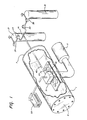
- FIGURE 1 is a partial phantom view of a vacuum deposition system for applying the coating to the substrate.
- FIGURE 2 is a partial isometric view, not to scale, of a coated plastic lens.
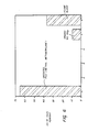
- FIGURE 3 is a partial isometric view of a bi-layer windshield having the hard coating on the exposed surface of the plastic.
- FIGURE 4 is a partial cutaway view through cutting plane 4-4' of the windshield of Figure 3 showing the glass substrate, the polyvinyl alcohol adhesive, the polyurethane bi-layer, and the hard coating.
- FIGURE 5 is a flow chart of the method of forming the coated article of the invention.
- FIGURE 6 is a bar graph of the comparison of the increase in haze by the Falling Sand Test with SiC #80 by ASTM Standard 968 for uncoated poly(methyl methacrylate), the amorphous carbon - SiO2 compositional graded coating of the invention, and float glass.
- FIGURE 7 is a graph of haze versus strokes by ASTM Standard F-735 for polycarbonate, poly(methyl methacrylate), float glass, and the amorphous carbon - SiO2 compositionally graded coating of the invention.
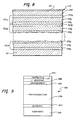
- FIGURE 8 is a greatly enlarged, fragmentary, cross sectional view of a continuous length of large area semiconductor material comprising a plurality of stacked n-i-p photovoltaic cells.
- FIGURE 9 is a greatly enlarged, fragmentary, cross sectional view of a portion of an electro photographic drum.
- a coated article having a substrate, e.g, a polymeric substrate or a semiconductor substrate, with an adherent, abrasion resistant, optically transmissive coating thereon.
- the hard coating is substantially colorless and transparent in the visible portion of the spectrum, and partially absorbing in the ultraviolet wave portion of the spectrum.
- the light transmission integrated over the visible spectrum is above about 87 percent when determined by the method of ASTM D-1003.
- the light transmission at 550 nanometers is above about 89 percent when determined using a spectrophotometer.
- the microwave deposition of a carbon-silicon dioxide coating having graded order or composition allows a relatively thick but substantially colorless coating to be applied to a substrate that is mis-matched in a physical parameter, as modulus of elasticity, coefficient of thermal expansion, lattice parameter, size of microcrystalline inclusions, or volume fraction of microcrystalline material, to be deposited quickly and without deformation or degradation of the substrate or delamination of the coating.
- the coating is thick enough to be abrasion and impact resistant and to avoid or relieve stresses between the substrate and the mismatched, outer portion of the coating, and thin enough to be light transmissive.
- the coating is on the order of about 1 to about 10 ⁇ m thick and preferably from about 2 to about 5 ⁇ m thick, with the compositionally and/or structurally graded portion of the coating being thick enough to modulate the mis-match of parameters and provide stress relief, e. g. from several atomic diameters to several ⁇ m, e.g., up to 10 ⁇ m.
- the outer portion of the coating may have a thickness such as to provide, in combination with the index of refraction thereof and optionally of the underlying portion, anti-reflective and/or selectively reflective properties.
- the thickness of the outer portion may have a thickness of an odd quarter wave length to provide interference colors.
- the coating is formed of amorphous carbon at the substrate and silicon dioxide remote therefrom. At the coating-substrate interface, the coating is substantially amorphous, characterized by the substantial absence of long range order although it may include more ordered regions and even crystalline or polycrystalline regions therein. The coating is graded in composition and/or structure remote from the substrate.
- silicon dioxide is meant both stoichiometric SiO2 and silicon suboxides.
- the thickness of the gradation from amorphous at the substrate to silicon dioxide, remote from the substrate is a function of, inter alia, the degree of mis-match of the properties, i.e. , lattice parameters, coefficients of elasticity, or thermal expansion coefficients, of the substrate and the hard coating, and may be from several atomic diameters to several ⁇ m.
- the adherent, and preferably substantially light transmitting and ultraviolet absorbing coating is prepared by microwave deposition.
- a deposition coating system is shown in Figure 1.
- the deposition coating system includes a vacuum chamber 1 , having end plates 5 and 7.
- the vacuum chamber 1 is evacuated by a vacuum pump 11.
- the vacuum chamber further includes means for feeding the reactive gas and inert gas, e.g. from tanks 21 and 31 , through valves and regulators 23 and 25, and 33 and 35, to a fitting, for example "tee" fitting 41, and from the "tee” fitting 41 into the vacuum chamber through vacuum line 43.
- the deposition system further includes a microwave antenna or a microwave horn 5l , and a microwave power supply 53.
- the microwave antenna 51 energizes the deposition gases, resulting in the formation of a plasma which then forms the coated articles 101.
- the process is characterized by initially depositing the coating at a low microwave energy. This provides the disordered, e.g. , amorphous, portion of the coating in contact with the substrate 121, or 221. Thereafter deposition is continued at a higher microwave energy to build up the coating.
- sputter etching is carried out to prepare the substrate.
- the sputter etching has been carried out with a 200 watt radio frequency signal, in argon at 10 ⁇ 4 to 10 ⁇ 6 atmospheres (10.1 to 0.101 Pa) for 5 to 20 minutes.
- inert gas and hydrocarbon are introduced into the vacuum chamber 1.
- the ratio of inert gas to hydrocarbon varies from 7:1 to 1:7 and preferably about 1:1.
- a gas flow rate of about 40 standard cubic centimeters (4 x 10 ⁇ 5m3) per minute provides efficient gas utilization.
- the residence of the gases is about 0.02 to about 0.10 seconds.
- the hydrocarbon may be a saturated gaseous hydrocarbon, as methane, ethane, propane, or butane, or unsaturated, low molecular weight, hydrocarbon gas as ethylene, propylene, butene, or butadiene or even acetylene.
- a saturated gaseous hydrocarbon as methane, ethane, propane, or butane, or unsaturated, low molecular weight, hydrocarbon gas as ethylene, propylene, butene, or butadiene or even acetylene.
- the silicon source is a silane.
- the silane is preferably a low molecular weight silane gas, for example monosilane, SiH4, or disilane Si2H6 and the oxidant for SiO2 formation may be O2 or N2O, with N2O preferred.
- the inert gas may be helium, neon, argon or krypton. Generally, for reasons of cost and energy transfer efficiency, the inert gas is argon.
- a microwave plasma is established and maintained at a relatively low energy and high pressure to provide initial adhesion without deformation of the plastic substrate 121,221.
- This power is generally on the order of about 50 to 75 watts.
- the pressure is from 100 to 200 millitorrs (13.3 to 26.7 Pa). This low microwave energy and high pressure regime is maintained for about 15 to 30 minutes to establish a relatively thin, disordered, adherent coating.
- the next step in the process is to increase the power and reduce the pressure while building up the thick coating without damaging, degrading, or deforming the substrate 121, 221.
- the power increase may be done as a single step, or as ramp. That is, the power increase may be instantaneous, or it may be carried out over a period of as long as 3 to 5 minutes.
- the thermal inertia, thermal capacitance, or time lag of the deposition process provides a continuous or semicontinuous change in the composition, structure, or parameters within the coating, i.e., grading.
- the power is increased to more than 75 watts e.g. to 100 watts or more for further build up of the coating.
- the pressure is reduced to about 25 to 75 millitorrs (3.3 to 10.0 Pa).
- the high power, low pressure deposition is continued far a period of about 15 to 250 minutes whereby to get a thick coating having the desired properties. These are the properties associated with disordered silicon dioxide.
- this second stage of the deposition there may be partial replacement of the hydrocarbon with silane.
- the deposition parameters are controlled so as to match the rates of ordered material growth and disordered material plasma etching. In this way disordered material is continuously removed while ordered material grows continuously.
- Thermal degrdation includes melting, softening, deformation, deleterious phase changes and transformations, decomposition, depolymerization, outgassing, and the like.
- Figure 2 shows an ophthalmic lens 101 having a plastic substrate 121.
- the plastic substrate may be a polycarbonate a polyacrylate, such as poly(methyl methacrylate) or a poly(allyl carbonate) such as PPG Industries "CR-39"(R) diethylene glycol bis (allyl carbonate), polymerized with a suitable peroxide initiator to form a hard, substantially light transmissive polymer.
- the coating 111 is generally from about 1 to about 10 ⁇ m thick and particularly from about 2 to about 5 ⁇ m thick. It comprises carbon-silicon dioxide where the silicon dioxide is graded from substantially no silicon dioxide in the first ⁇ m to an increasing amount measured outward from the substrate 121.
- the plastic substrate could also be a plastic optical fiber, or laser mirror, or a plastic sheet, as a door, window, sun roof insert, or the like.
- the coated article may be a glass-plastic laminate having the contemplated hard coating on the surface of the plastic unprotected from the glass.
- exemplary is a windshield 201 as shown in Figure 3 and 4.
- the article could be a window, a storm door glazing unit, or a sliding door glazing unit.
- the windshield 201 includes a glass substrate 221 with a thin adhesive layer 223 of, for example, polyvinyl alcohol, and a plastic film 225, for example a substantially water white polyurethane.
- the hard coating 231 is on the unprotected surface of the plastic layer 225. This results in a significant reduction in abrasion and scratching of the plastic 225.
- Coupons of uncoated polycarbonate, and uncoated poly(methyl methacrylate), having the compositionally graded amorphous carbon - silicon dioxide coating were tested for percent haze by the method of ASTM Standard F-735. The results are plotted in Figure 7.
- the substrate may be a metal substrate or a semiconductor substrate, e.g., a soft metal substrate, as an aluminum or copper substrate, or an amorphous alloy of silicon, where the coating is an amorphous material in contact with the substrate.
- a metal substrate or a semiconductor substrate e.g., a soft metal substrate, as an aluminum or copper substrate, or an amorphous alloy of silicon, where the coating is an amorphous material in contact with the substrate.
- Figure 8 illustrates a large-area-body of semiconductor material configured as a photovoltaic cell formed of a plurality of successive n-i-p type layers each of which includes preferably an amorphous thin film semiconductor alloy material and the compositionally or structurally graded external coating of this invention.
- Figure 8 shows an n-i-p type photovoltaic device, such as a solar cell or imager, made up of a plurality of stacked individual n-i-p type cells 312 a , 312 b and 312 c .
- a substrate 311 which may be transparent or formed from a metallic material such as stainless steel , aluminum, tantalum, molybdenum, chrome or metallic particles embedded within an insulator.
- a substrate shall include not only a flexible film, but also any element added thereto by preliminary processing.
- Each of the cells 312 a , 312 b and 312 c are preferably fabricated with a thin film semiconductor body containing at least a silicon alloy.
- Each of the semiconductor bodies includes a p-type conductivity semiconductor layer 320 a , 320 b and 320 c ; a substantially intrinsic semiconductor layer 318 a , 318 b and 318 c .
- the intrinsic layer may include traces of n-type or p-type dopant material without forfeiting its characteristic neutrality. Hence, it may be referred to herein as a "substantially intrinsic layer".
- cell 312 b is an intermediate cell and as indicated in Figure 8, additional intermediate cells may be stacked atop the illustrated cells.
- a further deposition process may be either performed in a separate environment or part of a continuous process.
- a TCO (transparent conductive oxide) layer 322 is added. This layer 322 forms the upper electrode of the photovoltaic device.
- the large-area device 310 functions as a photovoltaic cell; however, it is frequently desirable to configure the large area device 310 into a plurality of smaller area cells.
- the photovoltaic cell illustrated in Figure 8 is preferably modularized for delivery to the ultimate consumer.
- plastic laminates such as TEDLAR (registered trademark of Dupont Corp.) were used to encapsulate the upper surface of said cell.
- plastic encapsulants tended to deteriorate with age, required complicated processing techniques and added unnecessary weight to the lightweight cells described hereinabove.
- coatings which are hard, wear-resistant, impervious to atmospheric contaminants, and ameanable coating by continuous vapor deposition processes.
- such lightweight, ultra-wear resistant coatings 331 may be vapor deposited upon the cell.
- a layer of graded composition and/or structure can be deposited by a roll-to-roll process so as to be integrally affixed to the top surface of the TCO layer of the photovoltaic cell.
- Figure 9 illustrates a section 550 of the surface of an electrophotographic drum.
- the drum has a photoconductive portion formed of the drum substrate 552, a bottom blocking layer 554, a photoconductive layer 556, an optional enhancement layer 560, a top blocking layer 558, and a transparent, hard layer 570 graded in composition and/or structure.
- the substrate 552 can be formed of any convenient material which is either conductive, such as a metal, or has a conductive coating formed thereon, such as glass or a polymer.
- the first or bottom blocking layer 554 is formed of either an n-type or a p-type microcrystalline or amorphous silicon, hydrogen and/or fluorine alloy. When the device 550 is a positively charged device the bottom blocking layer 554 prevents electron injection from the substrate 552 into the photoconductive layer 556. When the device 550 is a negatively charged device, the bottom blocking layer 554 prevents hole injection from the substrate 552 into the photoconductive layer 556. This layer is from 5nm (50 Angstroms) to 1 ⁇ m thick.
- the photoconductive layer 556 is 10 to 25 ⁇ m thick.
- the 10 ⁇ m thickness is to ensure a saturation voltage of about 350 volts.
- the photoconductive alloy can sustain an electric field of up to about 35 to 70 volts per ⁇ m of thickness.
- the layer 556 preferably is formed by microwave deposition from a reaction gas mixture of SiH4 or SiH4 and/or SiF4 with a small amount of p-type dopant to form a substantially intrinsic or slightly pi-type alloy.
- the alloy with no dopant is slightly n-type exhibiting a Delta (E) of 0.7 eV.
- the addition of the small amount of p-type dopant changes Delta (E) to about 1.0 eV.
- An enhanced top blocking layer 560 is deposited before the layer 558.
- the microwave deposition provides a high quality alloy layer 556
- the alloy layer 556 can contain more defects than a properly deposited RF layer.
- the layer 560 is then deposited by a conventional RF plasma to provide a high quality layer with a density of states which is lower than the microwave deposited photoconductive layer 556.
- the RF layer 560 enhances the layer 558, because the lower density of states provides greater band bending and thus better charge retention, dark decay characteristics and freedom from fatiguing effects due to repeated light exposure and exposure due to certain atmospheric species which have been reported to reduce device performance.
- the effective overall deposition rate and reaction gas utilization is not lowered too significantly, since the layer 560 preferably is on the order of a depletion width thick, generally (1000 to 4000 Angstroms) 100 to 400 nm.
- the layer 560 can be deposited from the same reaction gas mixture as the photoconductive layer 556.
- the top blocking layer 558 is formed to provide a very hard surface as compared to any photoconductive material as for example silicon, or chalcogenides, such as Se or Se92Ti8.
- the layer 558 is chemically resistant to moisture and temperature effects to provide the member with improved stability.
- the layer has a band gap of greater than 2.0 eV.
- the herein contemplated, transparent protective layer 570 provides an added measure of durability and toughness. It is graded in composition and/or structure, i.e., from amorphous carbon at its interface with the top blocking layer 458 to amorphous SiO2 remote therefrom.
Landscapes
- Chemical & Material Sciences (AREA)
- Engineering & Computer Science (AREA)
- Organic Chemistry (AREA)
- Metallurgy (AREA)
- Materials Engineering (AREA)
- Physics & Mathematics (AREA)
- General Chemical & Material Sciences (AREA)
- Chemical Kinetics & Catalysis (AREA)
- Mechanical Engineering (AREA)
- Crystallography & Structural Chemistry (AREA)
- Optics & Photonics (AREA)
- General Physics & Mathematics (AREA)
- Plasma & Fusion (AREA)
- Inorganic Chemistry (AREA)
- Laminated Bodies (AREA)
- Photovoltaic Devices (AREA)
- Chemical Vapour Deposition (AREA)
- Application Of Or Painting With Fluid Materials (AREA)
- Materials For Medical Uses (AREA)
- Physical Vapour Deposition (AREA)
Claims (4)
- Ein beschichteter Gegenstand (101) mit einem Substrat (121) und einer Beschichtung (111) aus Siliciumdioxid und hierauf niedergeschlagenem Kohlenstoff, dadurch gekennzeichnet, daß die Beschichtung eine festhaftende, abriebfeste,im wesentlichen amorphe Beschichtung ist, die im Teil direkt an der Oberfläche des Substrats im wesentlichen aus Kohlenstoff besteht und die hiervon weg eine ansteigende SiOx-Konzentration aufweist, worbei x 1,60 bis 2,00 ist, und die Beschichtung eine Durchlässigkeit von mindestens 89% im sichtbaren Bereich des Spektrums bei einer Dicke von 2 bis 5 /um hat und eine Durchlässigkeit von weniger als 20% bei einer Wellenlänge von 380 Nanometer hat.
- Gegenstand gemäß Anspruch 1, dadurch gekennzeichnet, daß er ein Substrat aus Polymermaterial hat.
- Gegenstand gemäß Anspruch 2, dadurch gekennzeichnet, daß das Substrat-Polymermaterial ausgewählt ist aus der Gruppe bestehend aus den Polyacrylaten, den Polycarbonaten, den Poly(allyl)carbonaten und den Polyurethanen.
- Gegenstand gemäß Anspruch 1, dadurch gekennzeichnet, daß er ein metallisches Substrat oder ein Halbleitersubstrat aufweist.
Priority Applications (1)
| Application Number | Priority Date | Filing Date | Title |
|---|---|---|---|
| AT87308138T ATE65803T1 (de) | 1986-11-03 | 1987-09-15 | Ueberzogener gegenstand sowie verfahren zu seiner herstellung. |
Applications Claiming Priority (2)
| Application Number | Priority Date | Filing Date | Title |
|---|---|---|---|
| US06/926,271 US4777090A (en) | 1986-11-03 | 1986-11-03 | Coated article and method of manufacturing the article |
| US926271 | 1986-11-03 |
Publications (2)
| Publication Number | Publication Date |
|---|---|
| EP0267679A1 EP0267679A1 (de) | 1988-05-18 |
| EP0267679B1 true EP0267679B1 (de) | 1991-07-31 |
Family
ID=25452966
Family Applications (1)
| Application Number | Title | Priority Date | Filing Date |
|---|---|---|---|
| EP19870308138 Expired - Lifetime EP0267679B1 (de) | 1986-11-03 | 1987-09-15 | Überzogener Gegenstand sowie Verfahren zu seiner Herstellung |
Country Status (6)
| Country | Link |
|---|---|
| US (1) | US4777090A (de) |
| EP (1) | EP0267679B1 (de) |
| JP (1) | JPS63122533A (de) |
| AT (1) | ATE65803T1 (de) |
| CA (1) | CA1263928A (de) |
| DE (1) | DE3771843D1 (de) |
Cited By (3)
| Publication number | Priority date | Publication date | Assignee | Title |
|---|---|---|---|---|
| US6749813B1 (en) | 2000-03-05 | 2004-06-15 | 3M Innovative Properties Company | Fluid handling devices with diamond-like films |
| US7496255B2 (en) | 2000-03-05 | 2009-02-24 | 3M Innovative Properties Company | Radiation-transmissive films on glass articles |
| US9523516B2 (en) | 2008-12-30 | 2016-12-20 | 3M Innovative Properties Company | Broadband reflectors, concentrated solar power systems, and methods of using the same |
Families Citing this family (108)
| Publication number | Priority date | Publication date | Assignee | Title |
|---|---|---|---|---|
| JPH0676666B2 (ja) * | 1987-02-10 | 1994-09-28 | 株式会社半導体エネルギ−研究所 | 炭素膜作製方法 |
| US5051308A (en) * | 1987-08-24 | 1991-09-24 | General Electric Company | Abrasion-resistant plastic articles |
| NL8800911A (nl) * | 1987-09-30 | 1989-04-17 | Pelt & Hooykaas | Optisch element voor het behandelen van licht, werkwijze voor het vervaardigen van een dergelijk optisch element en een dergelijke optische elementen omvattende laseropstelling. |
| US4783374A (en) * | 1987-11-16 | 1988-11-08 | Ovonic Synthetic Materials Company | Coated article and method of manufacturing the article |
| JP2610469B2 (ja) * | 1988-02-26 | 1997-05-14 | 株式会社 半導体エネルギー研究所 | 炭素または炭素を主成分とする被膜を形成する方法 |
| US6224952B1 (en) * | 1988-03-07 | 2001-05-01 | Semiconductor Energy Laboratory Co., Ltd. | Electrostatic-erasing abrasion-proof coating and method for forming the same |
| US5190824A (en) * | 1988-03-07 | 1993-03-02 | Semiconductor Energy Laboratory Co., Ltd. | Electrostatic-erasing abrasion-proof coating |
| FR2631346B1 (fr) * | 1988-05-11 | 1994-05-20 | Air Liquide | Revetement protecteur multicouche pour substrat, procede de protection de substrat par depot par plasma d'un tel revetement, revetements obtenus et leurs applications |
| US5432003A (en) * | 1988-10-03 | 1995-07-11 | Crystallume | Continuous thin diamond film and method for making same |
| US5185179A (en) * | 1988-10-11 | 1993-02-09 | Semiconductor Energy Laboratory Co., Ltd. | Plasma processing method and products thereof |
| JPH02199099A (ja) * | 1988-10-21 | 1990-08-07 | Crystallume | 連続ダイヤモンド薄膜およびその製法 |
| GB8912470D0 (en) * | 1989-05-31 | 1989-07-19 | Stc Plc | Carbon coating of optical fibres |
| US5171607A (en) * | 1990-01-29 | 1992-12-15 | Bausch & Lomb Incorporated | Method of depositing diamond-like carbon film onto a substrate having a low melting temperature |
| EP0440326B1 (de) * | 1990-01-29 | 1994-12-14 | BAUSCH & LOMB INCORPORATED | Verfahren zum Aufdampfen eines diamantähnlichen Films auf ein niedrig schmelzendes Substrat |
| FR2661688B1 (fr) * | 1990-05-02 | 1992-07-17 | Air Liquide | Revetement multicouche pour substrat polycarbonate et procede d'elaboration d'un tel revetement. |
| JP2874298B2 (ja) * | 1990-07-24 | 1999-03-24 | 日本板硝子株式会社 | 磁気記録媒体およびその製造方法 |
| JP2929779B2 (ja) * | 1991-02-15 | 1999-08-03 | トヨタ自動車株式会社 | 炭素被膜付撥水ガラス |
| JPH07109034B2 (ja) * | 1991-04-08 | 1995-11-22 | ワイケイケイ株式会社 | 硬質多層膜形成体およびその製造方法 |
| JP2696015B2 (ja) * | 1991-09-13 | 1998-01-14 | 健 増本 | 傾斜機能薄膜 |
| US5442160A (en) * | 1992-01-22 | 1995-08-15 | Avco Corporation | Microwave fiber coating apparatus |
| US5910369A (en) | 1992-05-01 | 1999-06-08 | American Polymer, Inc. | Methods for protecting substrates with urethane protective coatings |
| US5470661A (en) * | 1993-01-07 | 1995-11-28 | International Business Machines Corporation | Diamond-like carbon films from a hydrocarbon helium plasma |
| US5249554A (en) * | 1993-01-08 | 1993-10-05 | Ford Motor Company | Powertrain component with adherent film having a graded composition |
| US5431963A (en) * | 1993-02-01 | 1995-07-11 | General Electric Company | Method for adhering diamondlike carbon to a substrate |
| US5618619A (en) * | 1994-03-03 | 1997-04-08 | Monsanto Company | Highly abrasion-resistant, flexible coatings for soft substrates |
| US5846649A (en) * | 1994-03-03 | 1998-12-08 | Monsanto Company | Highly durable and abrasion-resistant dielectric coatings for lenses |
| EP0723944A1 (de) * | 1995-01-26 | 1996-07-31 | Optical Coating Laboratory, Inc. | Verschleissfeste Fenster |
| US5543605A (en) * | 1995-04-13 | 1996-08-06 | Avco Corporation | Microwave fiber coating apparatus |
| EP0776989B1 (de) * | 1995-11-29 | 2002-03-27 | ANTEC Angewandte Neue Technologien GmbH | Verfahren zur Herstellung einer farbgebenden Beschichtung |
| US5900289A (en) * | 1995-11-29 | 1999-05-04 | Antec Angewandte Neue Technologien Gmbh | Method of producing a colorating coating |
| DE19625329A1 (de) * | 1996-06-25 | 1998-01-08 | Karlsruhe Forschzent | Stoffverbund und Verfahren zu dessen Herstellung |
| US6110329A (en) * | 1996-06-25 | 2000-08-29 | Forschungszentrum Karlsruhe Gmbh | Method of manufacturing a composite material |
| DE19635736C2 (de) * | 1996-09-03 | 2002-03-07 | Saxonia Umformtechnik Gmbh | Diamantähnliche Beschichtung |
| WO1998032312A1 (en) * | 1997-01-17 | 1998-07-23 | California Institute Of Technology | Microwave technique for brazing materials |
| US6066399A (en) * | 1997-03-19 | 2000-05-23 | Sanyo Electric Co., Ltd. | Hard carbon thin film and method of forming the same |
| DE19736449A1 (de) * | 1997-08-21 | 1999-02-25 | Gfe Met & Mat Gmbh | Verbundwerkstoff |
| US6287711B1 (en) | 1998-07-01 | 2001-09-11 | Front Edge Technology, Inc. | Wear-resistant coating and component |
| US6974629B1 (en) | 1999-08-06 | 2005-12-13 | Cardinal Cg Company | Low-emissivity, soil-resistant coating for glass surfaces |
| US6660365B1 (en) | 1998-12-21 | 2003-12-09 | Cardinal Cg Company | Soil-resistant coating for glass surfaces |
| US6964731B1 (en) | 1998-12-21 | 2005-11-15 | Cardinal Cg Company | Soil-resistant coating for glass surfaces |
| US6389100B1 (en) | 1999-04-09 | 2002-05-14 | Osmic, Inc. | X-ray lens system |
| US6368664B1 (en) | 1999-05-03 | 2002-04-09 | Guardian Industries Corp. | Method of ion beam milling substrate prior to depositing diamond like carbon layer thereon |
| US6312808B1 (en) | 1999-05-03 | 2001-11-06 | Guardian Industries Corporation | Hydrophobic coating with DLC & FAS on substrate |
| US6461731B1 (en) | 1999-05-03 | 2002-10-08 | Guardian Industries Corp. | Solar management coating system including protective DLC |
| US6261693B1 (en) * | 1999-05-03 | 2001-07-17 | Guardian Industries Corporation | Highly tetrahedral amorphous carbon coating on glass |
| US6475573B1 (en) | 1999-05-03 | 2002-11-05 | Guardian Industries Corp. | Method of depositing DLC inclusive coating on substrate |
| US6280834B1 (en) | 1999-05-03 | 2001-08-28 | Guardian Industries Corporation | Hydrophobic coating including DLC and/or FAS on substrate |
| US6335086B1 (en) | 1999-05-03 | 2002-01-01 | Guardian Industries Corporation | Hydrophobic coating including DLC on substrate |
| US6277480B1 (en) | 1999-05-03 | 2001-08-21 | Guardian Industries Corporation | Coated article including a DLC inclusive layer(s) and a layer(s) deposited using siloxane gas, and corresponding method |
| US6447891B1 (en) | 1999-05-03 | 2002-09-10 | Guardian Industries Corp. | Low-E coating system including protective DLC |
| US6421417B1 (en) | 1999-08-02 | 2002-07-16 | Osmic, Inc. | Multilayer optics with adjustable working wavelength |
| US6696157B1 (en) | 2000-03-05 | 2004-02-24 | 3M Innovative Properties Company | Diamond-like glass thin films |
| US6875318B1 (en) | 2000-04-11 | 2005-04-05 | Metalbond Technologies, Llc | Method for leveling and coating a substrate and an article formed thereby |
| FR2809190B1 (fr) * | 2000-05-22 | 2002-08-09 | Centre Nat Rech Scient | Procede de fabrication d'un modulateur de transmission pour microlithographie en ultraviolet profond et modulateur obtenu par ce procede |
| EP1158088A3 (de) * | 2000-05-26 | 2003-01-22 | Voith Paper Patent GmbH | Verfahren und Vorrichtung zur Behandlung einer Faserstoffsuspension |
| US6524755B2 (en) | 2000-09-07 | 2003-02-25 | Gray Scale Technologies, Inc. | Phase-shift masks and methods of fabrication |
| US6870896B2 (en) | 2000-12-28 | 2005-03-22 | Osmic, Inc. | Dark-field phase contrast imaging |
| US6804324B2 (en) * | 2001-03-01 | 2004-10-12 | Osmo, Inc. | X-ray phase contrast imaging using a fabry-perot interferometer concept |
| US6510200B1 (en) | 2001-06-29 | 2003-01-21 | Osmic, Inc. | Multi-layer structure with variable bandpass for monochromatization and spectroscopy |
| US7106939B2 (en) * | 2001-09-19 | 2006-09-12 | 3M Innovative Properties Company | Optical and optoelectronic articles |
| US7371467B2 (en) * | 2002-01-08 | 2008-05-13 | Applied Materials, Inc. | Process chamber component having electroplated yttrium containing coating |
| US6643353B2 (en) | 2002-01-10 | 2003-11-04 | Osmic, Inc. | Protective layer for multilayers exposed to x-rays |
| US6905773B2 (en) * | 2002-10-22 | 2005-06-14 | Schlage Lock Company | Corrosion-resistant coatings and methods of manufacturing the same |
| US20050186415A1 (en) * | 2003-11-21 | 2005-08-25 | Mccormick Chris E. | Protective laminate for windshields |
| CA2550331A1 (en) | 2003-12-22 | 2005-07-14 | Cardinal Cg Compagny | Graded photocatalytic coatings |
| EP1773729B1 (de) | 2004-07-12 | 2007-11-07 | Cardinal CG Company | Wartungsarme beschichtungen |
| US8092660B2 (en) | 2004-12-03 | 2012-01-10 | Cardinal Cg Company | Methods and equipment for depositing hydrophilic coatings, and deposition technologies for thin films |
| US7923114B2 (en) | 2004-12-03 | 2011-04-12 | Cardinal Cg Company | Hydrophilic coatings, methods for depositing hydrophilic coatings, and improved deposition technology for thin films |
| US8679674B2 (en) | 2005-03-25 | 2014-03-25 | Front Edge Technology, Inc. | Battery with protective packaging |
| US7846579B2 (en) * | 2005-03-25 | 2010-12-07 | Victor Krasnov | Thin film battery with protective packaging |
| US20080206484A1 (en) * | 2005-05-31 | 2008-08-28 | The Regents Of The University Of California | Graphitized Carbon Coatings for Composite Electrodes |
| FR2895521B1 (fr) * | 2005-12-23 | 2008-02-01 | Essilor Int | Installation et procede de revetement pour lentille ophtalmique. |
| JP4911491B2 (ja) * | 2006-01-11 | 2012-04-04 | クラシエホームプロダクツ株式会社 | 除毛剤用器具 |
| JP2009534563A (ja) * | 2006-04-19 | 2009-09-24 | 日本板硝子株式会社 | 同等の単独の表面反射率を有する対向機能コーティング |
| US20080011599A1 (en) | 2006-07-12 | 2008-01-17 | Brabender Dennis M | Sputtering apparatus including novel target mounting and/or control |
| US20080185034A1 (en) * | 2007-02-01 | 2008-08-07 | Corio Ronald P | Fly's Eye Lens Short Focal Length Solar Concentrator |
| US7862927B2 (en) * | 2007-03-02 | 2011-01-04 | Front Edge Technology | Thin film battery and manufacturing method |
| US8870974B2 (en) * | 2008-02-18 | 2014-10-28 | Front Edge Technology, Inc. | Thin film battery fabrication using laser shaping |
| US7862627B2 (en) | 2007-04-27 | 2011-01-04 | Front Edge Technology, Inc. | Thin film battery substrate cutting and fabrication process |
| US8628645B2 (en) | 2007-09-04 | 2014-01-14 | Front Edge Technology, Inc. | Manufacturing method for thin film battery |
| KR101512166B1 (ko) | 2007-09-14 | 2015-04-14 | 카디날 씨지 컴퍼니 | 관리가 용이한 코팅 기술 |
| US8664524B2 (en) | 2008-07-17 | 2014-03-04 | Uriel Solar, Inc. | High power efficiency, large substrate, polycrystalline CdTe thin film semiconductor photovoltaic cell structures grown by molecular beam epitaxy at high deposition rate for use in solar electricity generation |
| EP2459913B1 (de) * | 2009-07-29 | 2018-09-05 | Waters Technologies Corporation | Dreh-schereinspritzventil mit beschichteter statoroberfläche |
| US8502494B2 (en) | 2009-08-28 | 2013-08-06 | Front Edge Technology, Inc. | Battery charging apparatus and method |
| CN102892706B (zh) * | 2010-03-03 | 2015-08-12 | 太阳化学工业株式会社 | 在由非晶质碳膜构成的层的固定化方法及层叠体 |
| US8770749B2 (en) | 2010-04-15 | 2014-07-08 | Oakley, Inc. | Eyewear with chroma enhancement |
| US20120098971A1 (en) * | 2010-10-22 | 2012-04-26 | Flir Systems, Inc. | Infrared binocular system with dual diopter adjustment |
| US8865340B2 (en) | 2011-10-20 | 2014-10-21 | Front Edge Technology Inc. | Thin film battery packaging formed by localized heating |
| EP3447563A1 (de) | 2011-10-20 | 2019-02-27 | Oakley, Inc. | Brille mit farbverstärkung |
| US9887429B2 (en) | 2011-12-21 | 2018-02-06 | Front Edge Technology Inc. | Laminated lithium battery |
| US8864954B2 (en) | 2011-12-23 | 2014-10-21 | Front Edge Technology Inc. | Sputtering lithium-containing material with multiple targets |
| US9257695B2 (en) | 2012-03-29 | 2016-02-09 | Front Edge Technology, Inc. | Localized heat treatment of battery component films |
| US9077000B2 (en) | 2012-03-29 | 2015-07-07 | Front Edge Technology, Inc. | Thin film battery and localized heat treatment |
| WO2013169987A1 (en) | 2012-05-10 | 2013-11-14 | Oakley, Inc. | Eyewear with laminated functional layers |
| DE102012010291A1 (de) * | 2012-05-18 | 2013-11-21 | Jenoptik Optical Systems Gmbh | Hybride DLC-Beschichtung für IR-Optiken |
| US9159964B2 (en) | 2012-09-25 | 2015-10-13 | Front Edge Technology, Inc. | Solid state battery having mismatched battery cells |
| US8753724B2 (en) | 2012-09-26 | 2014-06-17 | Front Edge Technology Inc. | Plasma deposition on a partially formed battery through a mesh screen |
| US9356320B2 (en) | 2012-10-15 | 2016-05-31 | Front Edge Technology Inc. | Lithium battery having low leakage anode |
| US9731456B2 (en) | 2013-03-14 | 2017-08-15 | Sabic Global Technologies B.V. | Method of manufacturing a functionally graded article |
| US9575335B1 (en) | 2014-01-10 | 2017-02-21 | Oakley, Inc. | Eyewear with chroma enhancement for specific activities |
| WO2016077431A2 (en) | 2014-11-13 | 2016-05-19 | Oakley, Inc. | Variable light attenuation eyewear with color enhancement |
| US10871661B2 (en) | 2014-05-23 | 2020-12-22 | Oakley, Inc. | Eyewear and lenses with multiple molded lens components |
| US10008739B2 (en) | 2015-02-23 | 2018-06-26 | Front Edge Technology, Inc. | Solid-state lithium battery with electrolyte |
| WO2018093985A1 (en) | 2016-11-17 | 2018-05-24 | Cardinal Cg Company | Static-dissipative coating technology |
| US20180224087A1 (en) * | 2017-04-03 | 2018-08-09 | Robe Lighting S.R.O. | Lens Protection for High Intensity Luminaires |
| US12124116B2 (en) | 2017-10-20 | 2024-10-22 | Luxottica S.R.L. | Eyewear with variable transmission lens |
| US11112622B2 (en) | 2018-02-01 | 2021-09-07 | Luxottica S.R.L. | Eyewear and lenses with multiple molded lens components |
| CN118913470B (zh) * | 2024-07-18 | 2026-02-10 | 中国计量科学研究院 | 一种负温度系数热敏电阻温度传感器及其制造方法和应用 |
Family Cites Families (7)
| Publication number | Priority date | Publication date | Assignee | Title |
|---|---|---|---|---|
| US4504519A (en) * | 1981-10-21 | 1985-03-12 | Rca Corporation | Diamond-like film and process for producing same |
| EP0078541B1 (de) * | 1981-11-04 | 1991-01-16 | Kanegafuchi Kagaku Kogyo Kabushiki Kaisha | Biegsame photovoltaische Einrichtung |
| GB2114963B (en) * | 1981-12-18 | 1985-02-06 | Ion Tech Ltd | A method for providing a surface with a transparent carbon coating |
| DE3316693A1 (de) * | 1983-05-06 | 1984-11-08 | Leybold-Heraeus GmbH, 5000 Köln | Verfahren zum herstellen von amorphen kohlenstoffschichten auf substraten und durch das verfahren beschichtete substrate |
| DE3577730D1 (de) * | 1984-03-03 | 1990-06-21 | Stc Plc | Beschichtungsverfahren. |
| US4698256A (en) * | 1984-04-02 | 1987-10-06 | American Cyanamid Company | Articles coated with adherent diamondlike carbon films |
| US4663183A (en) * | 1984-09-10 | 1987-05-05 | Energy Conversion Devices, Inc. | Glow discharge method of applying a carbon coating onto a substrate |
-
1986
- 1986-11-03 US US06/926,271 patent/US4777090A/en not_active Expired - Lifetime
-
1987
- 1987-09-02 CA CA000545999A patent/CA1263928A/en not_active Expired
- 1987-09-15 DE DE8787308138T patent/DE3771843D1/de not_active Expired - Lifetime
- 1987-09-15 AT AT87308138T patent/ATE65803T1/de not_active IP Right Cessation
- 1987-09-15 EP EP19870308138 patent/EP0267679B1/de not_active Expired - Lifetime
- 1987-11-02 JP JP62278125A patent/JPS63122533A/ja active Pending
Cited By (3)
| Publication number | Priority date | Publication date | Assignee | Title |
|---|---|---|---|---|
| US6749813B1 (en) | 2000-03-05 | 2004-06-15 | 3M Innovative Properties Company | Fluid handling devices with diamond-like films |
| US7496255B2 (en) | 2000-03-05 | 2009-02-24 | 3M Innovative Properties Company | Radiation-transmissive films on glass articles |
| US9523516B2 (en) | 2008-12-30 | 2016-12-20 | 3M Innovative Properties Company | Broadband reflectors, concentrated solar power systems, and methods of using the same |
Also Published As
| Publication number | Publication date |
|---|---|
| EP0267679A1 (de) | 1988-05-18 |
| CA1263928C (en) | 1989-12-19 |
| DE3771843D1 (de) | 1991-09-05 |
| CA1263928A (en) | 1989-12-19 |
| JPS63122533A (ja) | 1988-05-26 |
| ATE65803T1 (de) | 1991-08-15 |
| US4777090A (en) | 1988-10-11 |
Similar Documents
| Publication | Publication Date | Title |
|---|---|---|
| EP0267679B1 (de) | Überzogener Gegenstand sowie Verfahren zu seiner Herstellung | |
| CA1325793C (en) | Plasma deposited coatings and low temperature, plasma method of making same | |
| EP0317134B1 (de) | Beschichteter Gegenstand und Verfahren zu seiner Herstellung | |
| US6380480B1 (en) | Photoelectric conversion device and substrate for photoelectric conversion device | |
| US4939043A (en) | Optically transparent electrically conductive semiconductor windows | |
| US4869755A (en) | Encapsulation of a photovoltaic element | |
| US20090258205A1 (en) | Transparent substrate with transparent conductive film, method of manufacturing the same, and photoelectric conversion element including the substrate | |
| CN103201845A (zh) | 电子制品及形成方法 | |
| Sha et al. | Carbon-rich amorphous silicon carbide and silicon carbonitride films for silicon-based photoelectric devices and optical elements: Application from UV to mid-IR spectral range | |
| US4285762A (en) | Plasma etching of amorphous silicon (SE-35) | |
| US6238832B1 (en) | Electrophotographic photosensitive member | |
| US20110102926A1 (en) | Mirror and process for obtaining a mirror | |
| CN100423136C (zh) | 透明导电性基板及其制造方法、和光电转换元件 | |
| US20110056549A1 (en) | Thin-film solar module and method of making | |
| EP2351091B1 (de) | Photoelektrische Mehrfachsperrschichtanordnung und Prozess zu ihrer Herstellung | |
| US4726851A (en) | Amorphous silicon semiconductor film and production process thereof | |
| EP0438398B1 (de) | Durchsichtige, elektrisch leitende halbleiterfenster und herstellungsverfahren | |
| US20090071535A1 (en) | Antireflective coating on solar cells and method for the production of such an antireflective coating | |
| JP2001060707A (ja) | 光電変換装置 | |
| US20140230893A1 (en) | Boron nitride anti-reflection coatings and methods | |
| JPH0477281B2 (de) | ||
| Brierley et al. | Diamond coatings for large-area IR windows | |
| Demichelis et al. | Magnetron‐sputtered amorphous silicon | |
| EP2545588B1 (de) | Transparentes glassubstrat in kombination mit einer transparenten elektrisch leitenden schicht mit verbesserten elektrischen eigenschaften | |
| Bdchle et al. | BUILDING BLOCKS FOR MICRO-CRYSTALLINE THIN FILM SI SOLAR CELLS ON GLASS SUBSTRATE |
Legal Events
| Date | Code | Title | Description |
|---|---|---|---|
| PUAI | Public reference made under article 153(3) epc to a published international application that has entered the european phase |
Free format text: ORIGINAL CODE: 0009012 |
|
| AK | Designated contracting states |
Kind code of ref document: A1 Designated state(s): AT BE CH DE ES FR GB GR IT LI LU NL SE |
|
| 17P | Request for examination filed |
Effective date: 19881110 |
|
| 17Q | First examination report despatched |
Effective date: 19900306 |
|
| GRAA | (expected) grant |
Free format text: ORIGINAL CODE: 0009210 |
|
| AK | Designated contracting states |
Kind code of ref document: B1 Designated state(s): AT BE CH DE ES FR GB GR IT LI LU NL SE |
|
| PG25 | Lapsed in a contracting state [announced via postgrant information from national office to epo] |
Ref country code: AT Effective date: 19910731 Ref country code: CH Effective date: 19910731 Ref country code: LI Effective date: 19910731 Ref country code: BE Effective date: 19910731 Ref country code: SE Effective date: 19910731 Ref country code: GR Free format text: LAPSE BECAUSE OF FAILURE TO SUBMIT A TRANSLATION OF THE DESCRIPTION OR TO PAY THE FEE WITHIN THE PRESCRIBED TIME-LIMIT Effective date: 19910731 Ref country code: IT Free format text: LAPSE BECAUSE OF FAILURE TO SUBMIT A TRANSLATION OF THE DESCRIPTION OR TO PAY THE FEE WITHIN THE PRE;WARNING: LAPSES OF ITALIAN PATENTS WITH EFFECTIVE DATE BEFORE 2007 MAY HAVE OCCURRED AT ANY TIME BEFORE 2007. THE CORRECT EFFECTIVE DATE MAY BE DIFFERENT FROM THE ONE RECORDED.SCRIBED TIME-LIMIT Effective date: 19910731 |
|
| REF | Corresponds to: |
Ref document number: 65803 Country of ref document: AT Date of ref document: 19910815 Kind code of ref document: T |
|
| REF | Corresponds to: |
Ref document number: 3771843 Country of ref document: DE Date of ref document: 19910905 |
|
| ET | Fr: translation filed | ||
| PG25 | Lapsed in a contracting state [announced via postgrant information from national office to epo] |
Ref country code: LU Free format text: LAPSE BECAUSE OF NON-PAYMENT OF DUE FEES Effective date: 19910930 |
|
| PG25 | Lapsed in a contracting state [announced via postgrant information from national office to epo] |
Ref country code: ES Free format text: LAPSE BECAUSE OF FAILURE TO SUBMIT A TRANSLATION OF THE DESCRIPTION OR TO PAY THE FEE WITHIN THE PRESCRIBED TIME-LIMIT Effective date: 19911111 |
|
| REG | Reference to a national code |
Ref country code: CH Ref legal event code: PL |
|
| PLBE | No opposition filed within time limit |
Free format text: ORIGINAL CODE: 0009261 |
|
| STAA | Information on the status of an ep patent application or granted ep patent |
Free format text: STATUS: NO OPPOSITION FILED WITHIN TIME LIMIT |
|
| 26N | No opposition filed | ||
| PGFP | Annual fee paid to national office [announced via postgrant information from national office to epo] |
Ref country code: NL Payment date: 19960624 Year of fee payment: 10 |
|
| PGFP | Annual fee paid to national office [announced via postgrant information from national office to epo] |
Ref country code: GB Payment date: 19960808 Year of fee payment: 10 |
|
| PGFP | Annual fee paid to national office [announced via postgrant information from national office to epo] |
Ref country code: FR Payment date: 19960910 Year of fee payment: 10 |
|
| PGFP | Annual fee paid to national office [announced via postgrant information from national office to epo] |
Ref country code: DE Payment date: 19960927 Year of fee payment: 10 |
|
| PG25 | Lapsed in a contracting state [announced via postgrant information from national office to epo] |
Ref country code: GB Free format text: LAPSE BECAUSE OF NON-PAYMENT OF DUE FEES Effective date: 19970915 |
|
| PG25 | Lapsed in a contracting state [announced via postgrant information from national office to epo] |
Ref country code: FR Free format text: THE PATENT HAS BEEN ANNULLED BY A DECISION OF A NATIONAL AUTHORITY Effective date: 19970930 |
|
| PG25 | Lapsed in a contracting state [announced via postgrant information from national office to epo] |
Ref country code: NL Free format text: LAPSE BECAUSE OF NON-PAYMENT OF DUE FEES Effective date: 19980401 |
|
| GBPC | Gb: european patent ceased through non-payment of renewal fee |
Effective date: 19970915 |
|
| NLV4 | Nl: lapsed or anulled due to non-payment of the annual fee |
Effective date: 19980401 |
|
| PG25 | Lapsed in a contracting state [announced via postgrant information from national office to epo] |
Ref country code: DE Free format text: LAPSE BECAUSE OF NON-PAYMENT OF DUE FEES Effective date: 19980603 |
|
| REG | Reference to a national code |
Ref country code: FR Ref legal event code: ST |