EP0078541B1 - Biegsame photovoltaische Einrichtung - Google Patents
Biegsame photovoltaische Einrichtung Download PDFInfo
- Publication number
- EP0078541B1 EP0078541B1 EP82110122A EP82110122A EP0078541B1 EP 0078541 B1 EP0078541 B1 EP 0078541B1 EP 82110122 A EP82110122 A EP 82110122A EP 82110122 A EP82110122 A EP 82110122A EP 0078541 B1 EP0078541 B1 EP 0078541B1
- Authority
- EP
- European Patent Office
- Prior art keywords
- semiconductor
- layer
- amorphous
- microcrystalline
- group
- Prior art date
- Legal status (The legal status is an assumption and is not a legal conclusion. Google has not performed a legal analysis and makes no representation as to the accuracy of the status listed.)
- Expired - Lifetime
Links
Images

Classifications
-
- H—ELECTRICITY
- H10—SEMICONDUCTOR DEVICES; ELECTRIC SOLID-STATE DEVICES NOT OTHERWISE PROVIDED FOR
- H10F—INORGANIC SEMICONDUCTOR DEVICES SENSITIVE TO INFRARED RADIATION, LIGHT, ELECTROMAGNETIC RADIATION OF SHORTER WAVELENGTH OR CORPUSCULAR RADIATION
- H10F71/00—Manufacture or treatment of devices covered by this subclass
- H10F71/10—Manufacture or treatment of devices covered by this subclass the devices comprising amorphous semiconductor material
- H10F71/103—Manufacture or treatment of devices covered by this subclass the devices comprising amorphous semiconductor material including only Group IV materials
-
- H—ELECTRICITY
- H10—SEMICONDUCTOR DEVICES; ELECTRIC SOLID-STATE DEVICES NOT OTHERWISE PROVIDED FOR
- H10F—INORGANIC SEMICONDUCTOR DEVICES SENSITIVE TO INFRARED RADIATION, LIGHT, ELECTROMAGNETIC RADIATION OF SHORTER WAVELENGTH OR CORPUSCULAR RADIATION
- H10F10/00—Individual photovoltaic cells, e.g. solar cells
- H10F10/10—Individual photovoltaic cells, e.g. solar cells having potential barriers
- H10F10/17—Photovoltaic cells having only PIN junction potential barriers
-
- H—ELECTRICITY
- H10—SEMICONDUCTOR DEVICES; ELECTRIC SOLID-STATE DEVICES NOT OTHERWISE PROVIDED FOR
- H10F—INORGANIC SEMICONDUCTOR DEVICES SENSITIVE TO INFRARED RADIATION, LIGHT, ELECTROMAGNETIC RADIATION OF SHORTER WAVELENGTH OR CORPUSCULAR RADIATION
- H10F19/00—Integrated devices, or assemblies of multiple devices, comprising at least one photovoltaic cell covered by group H10F10/00, e.g. photovoltaic modules
- H10F19/30—Integrated devices, or assemblies of multiple devices, comprising at least one photovoltaic cell covered by group H10F10/00, e.g. photovoltaic modules comprising thin-film photovoltaic cells
-
- H—ELECTRICITY
- H10—SEMICONDUCTOR DEVICES; ELECTRIC SOLID-STATE DEVICES NOT OTHERWISE PROVIDED FOR
- H10F—INORGANIC SEMICONDUCTOR DEVICES SENSITIVE TO INFRARED RADIATION, LIGHT, ELECTROMAGNETIC RADIATION OF SHORTER WAVELENGTH OR CORPUSCULAR RADIATION
- H10F19/00—Integrated devices, or assemblies of multiple devices, comprising at least one photovoltaic cell covered by group H10F10/00, e.g. photovoltaic modules
- H10F19/90—Structures for connecting between photovoltaic cells, e.g. interconnections or insulating spacers
- H10F19/902—Structures for connecting between photovoltaic cells, e.g. interconnections or insulating spacers for series or parallel connection of photovoltaic cells
-
- H—ELECTRICITY
- H10—SEMICONDUCTOR DEVICES; ELECTRIC SOLID-STATE DEVICES NOT OTHERWISE PROVIDED FOR
- H10F—INORGANIC SEMICONDUCTOR DEVICES SENSITIVE TO INFRARED RADIATION, LIGHT, ELECTROMAGNETIC RADIATION OF SHORTER WAVELENGTH OR CORPUSCULAR RADIATION
- H10F77/00—Constructional details of devices covered by this subclass
- H10F77/10—Semiconductor bodies
- H10F77/16—Material structures, e.g. crystalline structures, film structures or crystal plane orientations
- H10F77/169—Thin semiconductor films on metallic or insulating substrates
- H10F77/1692—Thin semiconductor films on metallic or insulating substrates the films including only Group IV materials
-
- H—ELECTRICITY
- H10—SEMICONDUCTOR DEVICES; ELECTRIC SOLID-STATE DEVICES NOT OTHERWISE PROVIDED FOR
- H10F—INORGANIC SEMICONDUCTOR DEVICES SENSITIVE TO INFRARED RADIATION, LIGHT, ELECTROMAGNETIC RADIATION OF SHORTER WAVELENGTH OR CORPUSCULAR RADIATION
- H10F77/00—Constructional details of devices covered by this subclass
- H10F77/10—Semiconductor bodies
- H10F77/16—Material structures, e.g. crystalline structures, film structures or crystal plane orientations
- H10F77/169—Thin semiconductor films on metallic or insulating substrates
- H10F77/1698—Thin semiconductor films on metallic or insulating substrates the metallic or insulating substrates being flexible
-
- Y—GENERAL TAGGING OF NEW TECHNOLOGICAL DEVELOPMENTS; GENERAL TAGGING OF CROSS-SECTIONAL TECHNOLOGIES SPANNING OVER SEVERAL SECTIONS OF THE IPC; TECHNICAL SUBJECTS COVERED BY FORMER USPC CROSS-REFERENCE ART COLLECTIONS [XRACs] AND DIGESTS
- Y02—TECHNOLOGIES OR APPLICATIONS FOR MITIGATION OR ADAPTATION AGAINST CLIMATE CHANGE
- Y02E—REDUCTION OF GREENHOUSE GAS [GHG] EMISSIONS, RELATED TO ENERGY GENERATION, TRANSMISSION OR DISTRIBUTION
- Y02E10/00—Energy generation through renewable energy sources
- Y02E10/50—Photovoltaic [PV] energy
- Y02E10/548—Amorphous silicon PV cells
-
- Y—GENERAL TAGGING OF NEW TECHNOLOGICAL DEVELOPMENTS; GENERAL TAGGING OF CROSS-SECTIONAL TECHNOLOGIES SPANNING OVER SEVERAL SECTIONS OF THE IPC; TECHNICAL SUBJECTS COVERED BY FORMER USPC CROSS-REFERENCE ART COLLECTIONS [XRACs] AND DIGESTS
- Y02—TECHNOLOGIES OR APPLICATIONS FOR MITIGATION OR ADAPTATION AGAINST CLIMATE CHANGE
- Y02P—CLIMATE CHANGE MITIGATION TECHNOLOGIES IN THE PRODUCTION OR PROCESSING OF GOODS
- Y02P70/00—Climate change mitigation technologies in the production process for final industrial or consumer products
- Y02P70/50—Manufacturing or production processes characterised by the final manufactured product
Definitions
- Photovoltaic devices such as solar cells and photodetector are capable of converting solar radiation into usable electrical energy.
- the devices of this type have the large problem to be overcome that the generating cost is very large as compared with other means for generating electric energy.
- the main reasons are that the efficiency of utilizing a semiconductor material constituting the body of the device is low and much energy is required in producing the semiconductor material.
- amorphous silicon as a material of semiconductors, and this proposal has been considered as a technique having a possibility of overcoming the above problems.
- the amorphous silicon can be produced inexpensively and in large quantities by a glow discharge decomposition of silicon compounds such as silane and fluorosilane.
- a representative prior art solar cell using amorphous silicon is one prepared by forming a transparent electrode on a glass substrate capable of transmitting visible rays, forming a P-type amorphous silicon layer, an undoped amorphous silicon layer and a N-type amorphous silicon layer on the transparent electrode in that order by a glow discharge, and providing an ohmic contact electrode on the N-type layer. If light enters into the P-type layer, undoped layer and N-type layer through the glass substrate and transparent electrode, electron-hole pairs are mainly generated in the undoped layer. They are attracted by the PIN junction internal electric field created by the above-mentioned each layer to be transferred and is collected to the ohmic contact electrode to generate a voltage between the both electrodes. In solar cells of such a type, the open-circuit voltage is about 0.8V, and accordingly the cells are not used as they are as a power source for equipments requiring a large power source voltage.
- a solar cell using a polymer thin film rich in flexibility and heat resistance, such as polyimide, as a substrate is disclosed in Japanese Unexamined Patent Publication No. 149489/1979.
- the use of the polymer film as a substrate has the disadvantages that the substrate is curled during the deposition in the preparation of amorphous silicon and no flat solar cell is obtained, and that the substrate is not uniformly heated due to the deformation during the deposition and no uniform amorphous silicon layers are formed.
- a further object of the invention is to provide a flexible and heat resistant photovoltaic device.
- Another object of the invention is to provide a flexible, small-sized photovoltaic device having a plurality of generating zones on a single substrate.
- non-single-crystalline as used herein comprehends “amorphous”, “semiamorphous” and “microcrystalline”.
- any materials having an electric conductivity of not more than 10- 7 ( ⁇ ⁇ cm.) -1 , preferably not more than about 10- 9 ( ⁇ ⁇ cm.) -1 , at the time of light impinging can be employed as materials of the electric insulating thin film.
- a polymer having a flexibility and a heat resistance and an inorganic material having an electric conductivity of not more than about 10- 7 ( ⁇ ⁇ cm.)- 1 are employed as materials of the electric insulating layer of the substrate.
- Examples of the inorganic material film used as the electric insulating layer of the substrate are, for instance, a metal oxide such as SiO, Si0 2 , Al 2 O 3 , TiO or Ti02, crystalline or amorphous silicon carbide, silicon nitride and silicon carbide nitride, i.e. the hydrides thereof, i.e.
- the use of the combination of the polymer film and the inorganic material film as an electric insulation layer is advantageous in that there is avoided the lowering of the device characteristics which may occur, in case of using only a polymer film as an insulation layer, during the device fabrication due to generation of a gas from the polymer, occurrence of release at the interface between the insulation layer and the device or occurrence of cracks in the device, and in that the flexibility is improved by the decrease of the thickness of the inorganic material film and moreover the insulation and the surface smoothness of the substrate are improved.
- a substrate is designated as 1.
- An electric insulating layer 1b such as a flexible, heat resistant polymer thin film or an inorganic material thin film is formed on a metal foil1a.
- a lower electrode 2 which comes into ohmic contact with a P-type or N-type non-single-crystalline semiconductor is formed' in a desired pattern in a thickness of about 500 angstroms to about 1 pm. by deposition or sputtering.
- Fig. 2 is a schematic view of a vacuum apparatus for forming an amorphous silicon thin film and for fabricating the amorphous silicon photovoltaic device body 3 including the amorphous silicon thin film layers by a plasma glow discharge method or a sputtering deposition method.
- numerals 8 and 9 are electrodes and numeral 10 is a valve for introducing a predetermined gas into a vacuum chamber 7.
- a substrate 1 with a lower electrode 2 for the photovoltaic device is mounted on the electrode 9 with the lower electrode 2 facing up.
- a mixed gas of hydrogen or the like and an inert gas such as argon is introduced into the chamber through the valve 10 up to a pressure of 666.10- 3 to 13.3 Pa (5x10 -3 to 10- 1 Torr):
- a DC voltage or a RF voltage of 1 to several tens of MHz is then applied between the electrode 8 having a target and the electrode 9 on which the substrate with the lower electrode 2 for the photovoltaic device is mounted, thereby causing a plasma to generate in the chamber.
- a voltage of about 1 to 3 kV, an electric current of 100 to 300 mA and a power of 100 to 300 W are sufficient. If the above state is maintained for about 60 minutes, the amorphous silicon photovoltaic device body 3 including an intrinsic amorphous silicon thin film layer having a thickness of 0.1 to 1 um., a carrier lifetime of not less than 10 -7 second, a density of localized state of not more than 10 17 /cm 3 .eV and a carrier mobility of not less than 10- 3 cm 2 .N.sec.
- I-layer of the photovoltaic device there is employed, as an I-layer of the photovoltaic device, an intrinsic amorphous silicon (hereinafter referred to as "I-type a-Si") having a carrier lifetime of not less than about 10- 1 second, a density of localized state of not more than about 10" cm- 3 eV- 1 and a mobility of not less than 10- 3 cm 2 .N.sec., which is prepared by a glow discharge decomposition of silane or its derivatives, fluorosilane or its derivatives, or a mixture thereof.
- I-type a-Si intrinsic amorphous silicon having a carrier lifetime of not less than about 10- 1 second, a density of localized state of not more than about 10" cm- 3 eV- 1 and a mobility of not less than 10- 3 cm 2 .N.sec.
- Such an I-type a-Si layer is joined with P-type and N-type doped amorphous or microcrystalline silicon semiconductors to give a PIN junction structure.
- at least one of the P-layer and N-layer is a doped amorphous or microcrystalline semiconductor having an optical band gap of not less than about 1.85 eV, an electric conductivity of not less than about 10- 8 ( ⁇ ⁇ cm.)-' at 20°C. and a diffusion potential (exhibited in the PIN junction) of not less than about 1.1 volts.
- a semiconductor may be employed in both of the P-layer and the N-layer.
- the P-type and N-type amorphous or microcrystalline semiconductors are not particularly limited.
- Preferable amorphous or microcrystalline semiconductors include amorphous or microcrystalline silicon carbide of the formula: a-Si (1-x) C x' amorphous or microcrystalline silicon nitride of the formula: a-Si (1-y) N y , amorphous or microcrystalline silicon carbon nitride of the formula: a-Si (1-x-y) C x N y and the hydrides and fluorides thereof.
- amorphous or microcrystalline silicon compounds, hydrogenated ones and fluorinated ones are prepared by a glow discharge in a mixture of a hydrogen or fluorine compound of silicon such as silane or fluorosilane, a hydrogen or fluorine compound of carbon or nitrogen such as a hydrocarbon or ammonia, and a doping gas.
- a hydrogen or fluorine compound of silicon such as silane or fluorosilane
- a hydrogen or fluorine compound of carbon or nitrogen such as a hydrocarbon or ammonia
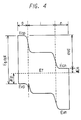
- this device is of the type that light impinges on the P-layer side, and is composed of metal foii 1a, electric insulating thin film layer 1b, electrode 2, N-type amorphous or microcrystalline silicon semiconductor 3a, I-type amorphous silicon 3b, P-type amorphous or microcrystalline semiconductor 3c and transparent electrode 4.
- the transparent electrode 4 is desired to be formed of ITO and Sn0 2 , especially Sn0 2 , and it is directly formed on the P-type amorphous semiconductor by vapor deposition.
- the thickness of the N-type amorphous or microcrystalline silicon semiconductor layer is not specifically limited, but is usually selected from about 15 to about 60 nm (150 to about 600 angstroms).
- a heterojunction of amorphous or microcrystalline semiconductors may be used on the opposite side to the light impinging side.
- a plurality of generating zones connected electrically with each other in series can be provided on a single substrate, namely un electrically insulated metal foil, for the purpose of providing a flexible, small-sized photovoltaic device capable of generating an increased photoelectromotive force.
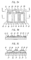
- Figs. 5A, 5B and 5C which show an embodiment of the photovoltaic device of the invention having a plurality of generating zones
- numeral 11 is a metal foil
- numeral 12 is an electric insulating thin film layer
- numerals 13, 14 and 15 are first, second and third generating zones formed on the insulation layer 17 of the substrate.
- Each of the generating zones is composed of a homojunction or heterojunction semiconductor layer 16, a first electrode 17 and a second electrode 18, both electrodes being positioned on the both sides of the layer 16.
- the homojunction or heterojunction layer 16 has, for instance, the structure as shown in Fig.
- a voltage is generated in each of the first, second and third generating zones. Since the generating zones 13,14 and 15 are connected to each other in series at the extending portions 19 and 20 of the first and second electrodes 17 and 18, the voltages generated at the respective zones are added, and the so added voltage is generated between the connecting poriton 21 as negative electrode and the extending portion 20 of the third generating zone as positive electrode.
- the distance between the adjacent generating zones is small, there may be observed the phenomenon that an electric current directlyflows between the both of the first electrodes 17 of the adjacent zones, or the both of the second electrodes 18 of the adjacent zones, namely occurrence of leakage current.
- the occurrence of leakage current can be substantially eliminated by providing the generating zones at a distance of at least 1 pm., since the resistance of the homojunction or heterojunction layer 16 is from several to several tens of M atthetime of light impinging. If necessary, the layer 16 may be separately formed in every generating zone, and the first electrode may be connected in series to the second electrode of the next adjacent generating zone.
- a plurality of generating zones each including a homojunction or heterojunction photovoltaic device body, are connected to each other in series, and accordingly a flexible, small-sized photovoltaic device capable of generating a desired voltage can be provided.
- the photovoltaic device can be fabricated in the same manner as a conventional photovoltaic device using a glass substrate, moreover on a mass production scale.
Landscapes
- Photovoltaic Devices (AREA)
Claims (10)
Priority Applications (1)
| Application Number | Priority Date | Filing Date | Title |
|---|---|---|---|
| EP89111929A EP0341756B2 (de) | 1981-11-04 | 1982-11-03 | Biegsame photovoltaische Vorrichtung |
Applications Claiming Priority (8)
| Application Number | Priority Date | Filing Date | Title |
|---|---|---|---|
| JP177685/81 | 1981-11-04 | ||
| JP56177685A JPS5878475A (ja) | 1981-11-04 | 1981-11-04 | 薄膜太陽電池 |
| JP203155/81 | 1981-12-15 | ||
| JP56203155A JPS58103178A (ja) | 1981-12-15 | 1981-12-15 | 耐熱性薄膜太陽電池 |
| JP56213119A JPS58115872A (ja) | 1981-12-28 | 1981-12-28 | 可撓性光起電力装置 |
| JP213119/81 | 1981-12-28 | ||
| JP60109/82 | 1982-04-09 | ||
| JP57060109A JPS58176977A (ja) | 1982-04-09 | 1982-04-09 | 可撓性薄膜光起電力装置 |
Related Child Applications (1)
| Application Number | Title | Priority Date | Filing Date |
|---|---|---|---|
| EP89111929.9 Division-Into | 1982-11-03 |
Publications (3)
| Publication Number | Publication Date |
|---|---|
| EP0078541A2 EP0078541A2 (de) | 1983-05-11 |
| EP0078541A3 EP0078541A3 (en) | 1986-03-26 |
| EP0078541B1 true EP0078541B1 (de) | 1991-01-16 |
Family
ID=27463862
Family Applications (1)
| Application Number | Title | Priority Date | Filing Date |
|---|---|---|---|
| EP82110122A Expired - Lifetime EP0078541B1 (de) | 1981-11-04 | 1982-11-03 | Biegsame photovoltaische Einrichtung |
Country Status (3)
| Country | Link |
|---|---|
| US (5) | US4612409A (de) |
| EP (1) | EP0078541B1 (de) |
| DE (2) | DE3280293D1 (de) |
Families Citing this family (186)
| Publication number | Priority date | Publication date | Assignee | Title |
|---|---|---|---|---|
| EP0078541B1 (de) * | 1981-11-04 | 1991-01-16 | Kanegafuchi Kagaku Kogyo Kabushiki Kaisha | Biegsame photovoltaische Einrichtung |
| GB2117971A (en) * | 1982-04-05 | 1983-10-19 | Hitachi Ltd | Amorphous silicon photovoltaic device |
| EP0103168A3 (de) * | 1982-09-10 | 1986-07-02 | Hitachi, Ltd. | Solarbatterie aus amorphem Silizium |
| US4594471A (en) * | 1983-07-13 | 1986-06-10 | Semiconductor Energy Laboratory Co., Ltd. | Photoelectric conversion device |
| US4514583A (en) * | 1983-11-07 | 1985-04-30 | Energy Conversion Devices, Inc. | Substrate for photovoltaic devices |
| JPH0652795B2 (ja) * | 1984-03-07 | 1994-07-06 | 太陽誘電株式会社 | 可撓性非晶質半導体太陽電池 |
| DE3626450A1 (de) * | 1986-08-05 | 1988-02-11 | Hans Joachim Dipl P Kirschning | Als solarzelle wirkendes bauteil von bauwerken und gebaeuden |
| US4777090A (en) * | 1986-11-03 | 1988-10-11 | Ovonic Synthetic Materials Company | Coated article and method of manufacturing the article |
| US4775425A (en) * | 1987-07-27 | 1988-10-04 | Energy Conversion Devices, Inc. | P and n-type microcrystalline semiconductor alloy material including band gap widening elements, devices utilizing same |
| MY104396A (en) * | 1988-02-05 | 1994-03-31 | Minnesota Mining & Mfg | Method for manufacturing an amorphous silicon thin film solar cell and schottky barrier diode on a common substrate. |
| US5155565A (en) * | 1988-02-05 | 1992-10-13 | Minnesota Mining And Manufacturing Company | Method for manufacturing an amorphous silicon thin film solar cell and Schottky diode on a common substrate |
| US4882239A (en) * | 1988-03-08 | 1989-11-21 | Minnesota Mining And Manufacturing Company | Light-rechargeable battery |
| WO1991017572A1 (fr) * | 1990-05-07 | 1991-11-14 | Canon Kabushiki Kaisha | Cellule solaire |
| JP2951060B2 (ja) * | 1990-12-27 | 1999-09-20 | 三洋電機株式会社 | 光起電力装置の製造方法 |
| US5112409A (en) * | 1991-01-23 | 1992-05-12 | Solarex Corporation | Solar cells with reduced recombination under grid lines, and method of manufacturing same |
| US6045652A (en) * | 1992-06-17 | 2000-04-04 | Micron Communications, Inc. | Method of manufacturing an enclosed transceiver |
| US5326652A (en) * | 1993-01-25 | 1994-07-05 | Micron Semiconductor, Inc. | Battery package and method using flexible polymer films having a deposited layer of an inorganic material |
| US7158031B2 (en) | 1992-08-12 | 2007-01-02 | Micron Technology, Inc. | Thin, flexible, RFID label and system for use |
| JP3098651B2 (ja) * | 1993-03-31 | 2000-10-16 | 松下電器産業株式会社 | 高分子電気デバイス |
| CA2120295C (en) * | 1993-04-21 | 1998-09-15 | Nazir P. Kherani | Nuclear batteries |
| US5350645A (en) * | 1993-06-21 | 1994-09-27 | Micron Semiconductor, Inc. | Polymer-lithium batteries and improved methods for manufacturing batteries |
| GB9401770D0 (en) * | 1994-01-31 | 1994-03-23 | Philips Electronics Uk Ltd | Manufacture of electronic devices comprising thin-film circuits |
| US6388366B1 (en) * | 1995-05-08 | 2002-05-14 | Wayne State University | Carbon nitride cold cathode |
| US7732243B2 (en) * | 1995-05-15 | 2010-06-08 | Daniel Luch | Substrate structures for integrated series connected photovoltaic arrays and process of manufacture of such arrays |
| US20080314433A1 (en) * | 1995-05-15 | 2008-12-25 | Daniel Luch | Substrate structures for integrated series connected photovoltaic arrays and process of manufacture of such arrays |
| AU756358B2 (en) * | 1996-09-05 | 2003-01-09 | Canon Kabushiki Kaisha | Photovoltaic element and method of and apparatus for manufacturing the same |
| JP3437386B2 (ja) * | 1996-09-05 | 2003-08-18 | キヤノン株式会社 | 光起電力素子、並びにその製造方法 |
| US5977476A (en) * | 1996-10-16 | 1999-11-02 | United Solar Systems Corporation | High efficiency photovoltaic device |
| JPH10321883A (ja) * | 1997-05-16 | 1998-12-04 | Semiconductor Energy Lab Co Ltd | 太陽電池およびその作製方法 |
| US6005184A (en) * | 1997-07-11 | 1999-12-21 | Space Systems/Loral, Inc. | Solar panels having improved heat dissipation properties |
| US6339385B1 (en) * | 1997-08-20 | 2002-01-15 | Micron Technology, Inc. | Electronic communication devices, methods of forming electrical communication devices, and communication methods |
| US6224016B1 (en) * | 1997-12-19 | 2001-05-01 | Sky Station International, Inc. | Integrated flexible solar cell material and method of production |
| US5986344A (en) | 1998-04-14 | 1999-11-16 | Advanced Micro Devices, Inc. | Anti-reflective coating layer for semiconductor device |
| US8076568B2 (en) | 2006-04-13 | 2011-12-13 | Daniel Luch | Collector grid and interconnect structures for photovoltaic arrays and modules |
| US8222513B2 (en) | 2006-04-13 | 2012-07-17 | Daniel Luch | Collector grid, electrode structures and interconnect structures for photovoltaic arrays and methods of manufacture |
| US20090107538A1 (en) * | 2007-10-29 | 2009-04-30 | Daniel Luch | Collector grid and interconnect structures for photovoltaic arrays and modules |
| US20080011350A1 (en) * | 1999-03-30 | 2008-01-17 | Daniel Luch | Collector grid, electrode structures and interconnect structures for photovoltaic arrays and other optoelectric devices |
| US20090111206A1 (en) | 1999-03-30 | 2009-04-30 | Daniel Luch | Collector grid, electrode structures and interrconnect structures for photovoltaic arrays and methods of manufacture |
| US7507903B2 (en) | 1999-03-30 | 2009-03-24 | Daniel Luch | Substrate and collector grid structures for integrated series connected photovoltaic arrays and process of manufacture of such arrays |
| US8138413B2 (en) | 2006-04-13 | 2012-03-20 | Daniel Luch | Collector grid and interconnect structures for photovoltaic arrays and modules |
| US6239352B1 (en) * | 1999-03-30 | 2001-05-29 | Daniel Luch | Substrate and collector grid structures for electrically interconnecting photovoltaic arrays and process of manufacture of such arrays |
| US8664030B2 (en) | 1999-03-30 | 2014-03-04 | Daniel Luch | Collector grid and interconnect structures for photovoltaic arrays and modules |
| US7635810B2 (en) * | 1999-03-30 | 2009-12-22 | Daniel Luch | Substrate and collector grid structures for integrated photovoltaic arrays and process of manufacture of such arrays |
| US6295818B1 (en) * | 1999-06-29 | 2001-10-02 | Powerlight Corporation | PV-thermal solar power assembly |
| US6641933B1 (en) * | 1999-09-24 | 2003-11-04 | Semiconductor Energy Laboratory Co., Ltd. | Light-emitting EL display device |
| US7898053B2 (en) * | 2000-02-04 | 2011-03-01 | Daniel Luch | Substrate structures for integrated series connected photovoltaic arrays and process of manufacture of such arrays |
| US20110067754A1 (en) * | 2000-02-04 | 2011-03-24 | Daniel Luch | Substrate structures for integrated series connected photovoltaic arrays and process of manufacture of such arrays |
| US8198696B2 (en) | 2000-02-04 | 2012-06-12 | Daniel Luch | Substrate structures for integrated series connected photovoltaic arrays and process of manufacture of such arrays |
| US7898054B2 (en) * | 2000-02-04 | 2011-03-01 | Daniel Luch | Substrate structures for integrated series connected photovoltaic arrays and process of manufacture of such arrays |
| US6618409B1 (en) * | 2000-05-03 | 2003-09-09 | Corning Incorporated | Passivation of semiconductor laser facets |
| JP4152574B2 (ja) | 2000-09-25 | 2008-09-17 | 株式会社半導体エネルギー研究所 | 薄膜の成膜方法および半導体装置の製造方法 |
| JP4093532B2 (ja) * | 2001-03-13 | 2008-06-04 | 独立行政法人理化学研究所 | アモルファス状金属酸化物の薄膜材料の製造方法 |
| US7442629B2 (en) | 2004-09-24 | 2008-10-28 | President & Fellows Of Harvard College | Femtosecond laser-induced formation of submicrometer spikes on a semiconductor substrate |
| US7057256B2 (en) | 2001-05-25 | 2006-06-06 | President & Fellows Of Harvard College | Silicon-based visible and near-infrared optoelectric devices |
| ATE528117T1 (de) * | 2001-08-30 | 2011-10-15 | Bayer Technology Services Gmbh | Verfahren zur herstellung von abformkörpern, insbesondere optischen strukturen, und deren verwendung |
| JP4276444B2 (ja) * | 2003-01-16 | 2009-06-10 | Tdk株式会社 | 鉄シリサイド膜の製造方法及び装置、光電変換素子の製造方法及び装置、並びに、光電変換装置の製造方法及び装置 |
| US7964789B2 (en) * | 2003-05-07 | 2011-06-21 | Imec | Germanium solar cell and method for the production thereof |
| US7960645B2 (en) | 2003-05-07 | 2011-06-14 | Imec | Germanium solar cell and method for the production thereof |
| US20060024442A1 (en) * | 2003-05-19 | 2006-02-02 | Ovshinsky Stanford R | Deposition methods for the formation of polycrystalline materials on mobile substrates |
| US20050139253A1 (en) * | 2003-12-31 | 2005-06-30 | Korman Charles S. | Solar cell assembly for use in an outer space environment or a non-earth environment |
| US7604843B1 (en) | 2005-03-16 | 2009-10-20 | Nanosolar, Inc. | Metallic dispersion |
| US8623448B2 (en) * | 2004-02-19 | 2014-01-07 | Nanosolar, Inc. | High-throughput printing of semiconductor precursor layer from chalcogenide microflake particles |
| US20070169809A1 (en) * | 2004-02-19 | 2007-07-26 | Nanosolar, Inc. | High-throughput printing of semiconductor precursor layer by use of low-melting chalcogenides |
| US7605328B2 (en) * | 2004-02-19 | 2009-10-20 | Nanosolar, Inc. | Photovoltaic thin-film cell produced from metallic blend using high-temperature printing |
| US20060060237A1 (en) * | 2004-09-18 | 2006-03-23 | Nanosolar, Inc. | Formation of solar cells on foil substrates |
| US8846141B1 (en) | 2004-02-19 | 2014-09-30 | Aeris Capital Sustainable Ip Ltd. | High-throughput printing of semiconductor precursor layer from microflake particles |
| US20070163642A1 (en) * | 2004-02-19 | 2007-07-19 | Nanosolar, Inc. | High-throughput printing of semiconductor precursor layer from inter-metallic microflake articles |
| US8309163B2 (en) * | 2004-02-19 | 2012-11-13 | Nanosolar, Inc. | High-throughput printing of semiconductor precursor layer by use of chalcogen-containing vapor and inter-metallic material |
| US20070163641A1 (en) * | 2004-02-19 | 2007-07-19 | Nanosolar, Inc. | High-throughput printing of semiconductor precursor layer from inter-metallic nanoflake particles |
| US20070163639A1 (en) * | 2004-02-19 | 2007-07-19 | Nanosolar, Inc. | High-throughput printing of semiconductor precursor layer from microflake particles |
| US7700464B2 (en) * | 2004-02-19 | 2010-04-20 | Nanosolar, Inc. | High-throughput printing of semiconductor precursor layer from nanoflake particles |
| US7663057B2 (en) * | 2004-02-19 | 2010-02-16 | Nanosolar, Inc. | Solution-based fabrication of photovoltaic cell |
| US8329501B1 (en) | 2004-02-19 | 2012-12-11 | Nanosolar, Inc. | High-throughput printing of semiconductor precursor layer from inter-metallic microflake particles |
| US8372734B2 (en) * | 2004-02-19 | 2013-02-12 | Nanosolar, Inc | High-throughput printing of semiconductor precursor layer from chalcogenide nanoflake particles |
| JP2005268405A (ja) * | 2004-03-17 | 2005-09-29 | Dow Corning Toray Co Ltd | 光学装置用金属ベース回路基板およびその製造方法 |
| KR100554179B1 (ko) * | 2004-06-09 | 2006-02-22 | 한국전자통신연구원 | 전도성 금속 기판을 포함하는 구부림이 가능한 염료감응태양전지 |
| US7732229B2 (en) * | 2004-09-18 | 2010-06-08 | Nanosolar, Inc. | Formation of solar cells with conductive barrier layers and foil substrates |
| US20090032108A1 (en) * | 2007-03-30 | 2009-02-05 | Craig Leidholm | Formation of photovoltaic absorber layers on foil substrates |
| JP2008514006A (ja) * | 2004-09-18 | 2008-05-01 | ナノソーラー インコーポレイテッド | 箔基板上の太陽電池の形成 |
| US7838868B2 (en) * | 2005-01-20 | 2010-11-23 | Nanosolar, Inc. | Optoelectronic architecture having compound conducting substrate |
| US8541048B1 (en) | 2004-09-18 | 2013-09-24 | Nanosolar, Inc. | Formation of photovoltaic absorber layers on foil substrates |
| US8927315B1 (en) | 2005-01-20 | 2015-01-06 | Aeris Capital Sustainable Ip Ltd. | High-throughput assembly of series interconnected solar cells |
| GB2430547A (en) * | 2005-09-20 | 2007-03-28 | Seiko Epson Corp | A method of producing a substrate having areas of different hydrophilicity and/or oleophilicity on the same surface |
| US9236512B2 (en) | 2006-04-13 | 2016-01-12 | Daniel Luch | Collector grid and interconnect structures for photovoltaic arrays and modules |
| US8729385B2 (en) | 2006-04-13 | 2014-05-20 | Daniel Luch | Collector grid and interconnect structures for photovoltaic arrays and modules |
| US9006563B2 (en) | 2006-04-13 | 2015-04-14 | Solannex, Inc. | Collector grid and interconnect structures for photovoltaic arrays and modules |
| US9865758B2 (en) | 2006-04-13 | 2018-01-09 | Daniel Luch | Collector grid and interconnect structures for photovoltaic arrays and modules |
| US8884155B2 (en) | 2006-04-13 | 2014-11-11 | Daniel Luch | Collector grid and interconnect structures for photovoltaic arrays and modules |
| US8822810B2 (en) | 2006-04-13 | 2014-09-02 | Daniel Luch | Collector grid and interconnect structures for photovoltaic arrays and modules |
| CN101421100B (zh) * | 2006-04-18 | 2013-03-27 | 陶氏康宁公司 | 用缩合固化的有机硅树脂组合物涂布的金属箔基底 |
| US20070243820A1 (en) | 2006-04-18 | 2007-10-18 | O'hagin Carolina | Automatic roof ventilation system |
| JP4933610B2 (ja) * | 2006-04-18 | 2012-05-16 | ダウ・コーニング・コーポレイション | 銅インジウム二セレン化物をベースとする光起電デバイス及びその光起電デバイスを作製する方法 |
| US8207442B2 (en) | 2006-04-18 | 2012-06-26 | Itn Energy Systems, Inc. | Reinforcing structures for thin-film photovoltaic device substrates, and associated methods |
| KR20090005184A (ko) * | 2006-04-18 | 2009-01-12 | 다우 코닝 코포레이션 | 구리 인듐 디셀레나이드-기재 광전지 장치 및 그의 제조 방법 |
| EP2021175A2 (de) * | 2006-04-18 | 2009-02-11 | Dow Corning Corporation | Mit kondensationsgehärteten silikonharzzusammensetzungen beschichtete metallfoliensubstrate |
| US20100059753A1 (en) * | 2006-06-16 | 2010-03-11 | Silk Displays | Matrix electronic devices using opaque substrates and fabrication method therefor |
| JP4789752B2 (ja) * | 2006-08-28 | 2011-10-12 | キヤノン株式会社 | 光電変換素子およびその製造方法 |
| WO2008036769A2 (en) | 2006-09-19 | 2008-03-27 | Itn Energy Systems, Inc. | Semi-transparent dual layer back contact for bifacial and tandem junction thin-film photovolataic devices |
| US8607510B2 (en) * | 2006-10-25 | 2013-12-17 | Gregory S. Daniels | Form-fitting solar panel for roofs and roof vents |
| JP2008112848A (ja) * | 2006-10-30 | 2008-05-15 | Shin Etsu Chem Co Ltd | 単結晶シリコン太陽電池の製造方法及び単結晶シリコン太陽電池 |
| JP2008112847A (ja) * | 2006-10-30 | 2008-05-15 | Shin Etsu Chem Co Ltd | 単結晶シリコン太陽電池の製造方法及び単結晶シリコン太陽電池 |
| JP2008112840A (ja) * | 2006-10-30 | 2008-05-15 | Shin Etsu Chem Co Ltd | 単結晶シリコン太陽電池の製造方法及び単結晶シリコン太陽電池 |
| JP2008112843A (ja) * | 2006-10-30 | 2008-05-15 | Shin Etsu Chem Co Ltd | 単結晶シリコン太陽電池の製造方法及び単結晶シリコン太陽電池 |
| JP5090716B2 (ja) * | 2006-11-24 | 2012-12-05 | 信越化学工業株式会社 | 単結晶シリコン太陽電池の製造方法 |
| JP5166745B2 (ja) * | 2007-03-07 | 2013-03-21 | 信越化学工業株式会社 | 単結晶シリコン太陽電池の製造方法 |
| JP5048380B2 (ja) * | 2007-04-09 | 2012-10-17 | 信越化学工業株式会社 | 単結晶シリコン太陽電池の製造方法 |
| CN101388417B (zh) * | 2007-09-14 | 2011-06-08 | 鸿富锦精密工业(深圳)有限公司 | 太阳能电池组件 |
| WO2009046178A1 (en) * | 2007-10-02 | 2009-04-09 | University Of Delaware | I-iii-vi2 photovoltaic absorber layers |
| JP5067815B2 (ja) * | 2007-11-22 | 2012-11-07 | シャープ株式会社 | 素子間配線部材、光電変換素子接続体および光電変換モジュール |
| DE212009000025U1 (de) * | 2008-01-31 | 2010-09-23 | Global Solar Energy. Inc., Tuscon | Dünnschicht-Solarzellen-Abfolge |
| CN102138220A (zh) * | 2008-08-29 | 2011-07-27 | 欧瑞康太阳Ip股份公司(特吕巴赫) | 用于为具有降低的光致衰退的光伏器件淀积非晶硅膜以改进稳定性能的方法 |
| KR20100028729A (ko) * | 2008-09-05 | 2010-03-15 | 삼성전자주식회사 | 복층 구조의 태양 전지 및 그 제조 방법 |
| WO2010039245A1 (en) * | 2008-09-30 | 2010-04-08 | Global Solar Energy, Inc. | Thin film solar cell string |
| JP2012513119A (ja) * | 2008-12-18 | 2012-06-07 | ファースト ソーラー インコーポレイテッド | 裏面金属コンタクトを含む光電変換装置 |
| TWI387391B (zh) * | 2009-03-04 | 2013-02-21 | Chung Shan Inst Of Science | 有機發光元件之製造方法 |
| US20110177622A1 (en) * | 2009-12-28 | 2011-07-21 | Global Solar Energy, Inc. | Apparatus and methods of mixing and depositing thin film photovoltaic compositions |
| US20100288631A1 (en) * | 2009-05-12 | 2010-11-18 | Solar Applied Materials Technology Corp. | Ceramic sputtering target assembly and a method for producing the same |
| US8247243B2 (en) * | 2009-05-22 | 2012-08-21 | Nanosolar, Inc. | Solar cell interconnection |
| US20110139225A1 (en) * | 2009-06-23 | 2011-06-16 | E. I. Du Pont De Nemours And Company | Shaped photovoltaic module |
| US20100326510A1 (en) * | 2009-06-27 | 2010-12-30 | Twin Creeks Technologies, Inc. | Thin semiconductor lamina adhered to a flexible substrate |
| FR2947257B1 (fr) * | 2009-06-30 | 2011-06-24 | Saint Gobain | Procede de fabrication d'un element de vitrage feuillete |
| WO2011022687A2 (en) * | 2009-08-20 | 2011-02-24 | Sionyx, Inc. | Laser processed heterojunction photovoltaic devices and associated methods |
| KR101074290B1 (ko) * | 2009-09-04 | 2011-10-18 | 한국철강 주식회사 | 광기전력 장치 및 광기전력 장치의 제조 방법 |
| US9673243B2 (en) | 2009-09-17 | 2017-06-06 | Sionyx, Llc | Photosensitive imaging devices and associated methods |
| US9911781B2 (en) | 2009-09-17 | 2018-03-06 | Sionyx, Llc | Photosensitive imaging devices and associated methods |
| US20110083724A1 (en) * | 2009-10-08 | 2011-04-14 | Ovshinsky Stanford R | Monolithic Integration of Photovoltaic Cells |
| US20110086462A1 (en) * | 2009-10-08 | 2011-04-14 | Ovshinsky Stanford R | Process for Manufacturing Solar Cells including Ambient Pressure Plasma Torch Step |
| EP2312641A1 (de) * | 2009-10-13 | 2011-04-20 | Ecole Polytechnique Fédérale de Lausanne (EPFL) | Vorrichtung mit elektrischen Kontakten und deren Herstellungsverfahren |
| US9012766B2 (en) | 2009-11-12 | 2015-04-21 | Silevo, Inc. | Aluminum grid as backside conductor on epitaxial silicon thin film solar cells |
| US8759664B2 (en) | 2009-12-28 | 2014-06-24 | Hanergy Hi-Tech Power (Hk) Limited | Thin film solar cell strings |
| US8692198B2 (en) | 2010-04-21 | 2014-04-08 | Sionyx, Inc. | Photosensitive imaging devices and associated methods |
| US9214576B2 (en) * | 2010-06-09 | 2015-12-15 | Solarcity Corporation | Transparent conducting oxide for photovoltaic devices |
| WO2011160130A2 (en) | 2010-06-18 | 2011-12-22 | Sionyx, Inc | High speed photosensitive devices and associated methods |
| US11139410B1 (en) * | 2010-07-06 | 2021-10-05 | The Boeing Company | Solar cell structure with back surface reflector |
| US9773928B2 (en) | 2010-09-10 | 2017-09-26 | Tesla, Inc. | Solar cell with electroplated metal grid |
| EP2617060A1 (de) * | 2010-09-14 | 2013-07-24 | E.I. Du Pont De Nemours And Company | Glasbeschichtete flexible polymersubstrate in pv-zellen |
| US9231139B2 (en) * | 2010-09-30 | 2016-01-05 | International Business Machines Corporation | Structure and design of concentrator solar cell assembly receiver substrate |
| US9800053B2 (en) | 2010-10-08 | 2017-10-24 | Tesla, Inc. | Solar panels with integrated cell-level MPPT devices |
| JP5609537B2 (ja) * | 2010-10-26 | 2014-10-22 | 住友化学株式会社 | 発電装置 |
| TWI406438B (zh) * | 2010-10-28 | 2013-08-21 | Hon Hai Prec Ind Co Ltd | 光電轉換元件及其製備方法 |
| US20120204941A1 (en) * | 2011-02-15 | 2012-08-16 | Cargo James T | Allotropic changes in si and use in fabricating materials for solar cells |
| US9054256B2 (en) | 2011-06-02 | 2015-06-09 | Solarcity Corporation | Tunneling-junction solar cell with copper grid for concentrated photovoltaic application |
| US9496308B2 (en) | 2011-06-09 | 2016-11-15 | Sionyx, Llc | Process module for increasing the response of backside illuminated photosensitive imagers and associated methods |
| JP2014525091A (ja) | 2011-07-13 | 2014-09-25 | サイオニクス、インク. | 生体撮像装置および関連方法 |
| US20130167916A1 (en) * | 2011-12-28 | 2013-07-04 | Taiwan Semiconductor Manufacturing Co., Ltd. | Thin film photovoltaic cells and methods of forming the same |
| US9064764B2 (en) | 2012-03-22 | 2015-06-23 | Sionyx, Inc. | Pixel isolation elements, devices, and associated methods |
| WO2013158796A1 (en) | 2012-04-17 | 2013-10-24 | Global Solar Energy, Inc. | Integrated thin film solar cell interconnection |
| US9876129B2 (en) * | 2012-05-10 | 2018-01-23 | International Business Machines Corporation | Cone-shaped holes for high efficiency thin film solar cells |
| CN104769726B (zh) * | 2012-09-05 | 2018-10-09 | 兹尼亚泰克有限公司 | 具有三维表面特征的光伏设备及制造该光伏设备的方法 |
| MX351564B (es) | 2012-10-04 | 2017-10-18 | Solarcity Corp | Dispositivos fotovoltaicos con rejillas metálicas galvanizadas. |
| US9865754B2 (en) | 2012-10-10 | 2018-01-09 | Tesla, Inc. | Hole collectors for silicon photovoltaic cells |
| US9281436B2 (en) | 2012-12-28 | 2016-03-08 | Solarcity Corporation | Radio-frequency sputtering system with rotary target for fabricating solar cells |
| US9412884B2 (en) | 2013-01-11 | 2016-08-09 | Solarcity Corporation | Module fabrication of solar cells with low resistivity electrodes |
| WO2014110520A1 (en) | 2013-01-11 | 2014-07-17 | Silevo, Inc. | Module fabrication of solar cells with low resistivity electrodes |
| US10074755B2 (en) | 2013-01-11 | 2018-09-11 | Tesla, Inc. | High efficiency solar panel |
| CN105164816B (zh) | 2013-01-28 | 2017-03-08 | 环球太阳能公司 | 光伏互连系统、装置和方法 |
| KR20150130303A (ko) | 2013-02-15 | 2015-11-23 | 사이오닉스, 아이엔씨. | 안티 블루밍 특성 및 관련 방법을 가지는 높은 동적 범위의 cmos 이미지 센서 |
| US9525097B2 (en) * | 2013-03-15 | 2016-12-20 | Nthdegree Technologies Worldwide Inc. | Photovoltaic module having printed PV cells connected in series by printed conductors |
| US9939251B2 (en) | 2013-03-15 | 2018-04-10 | Sionyx, Llc | Three dimensional imaging utilizing stacked imager devices and associated methods |
| US9624595B2 (en) | 2013-05-24 | 2017-04-18 | Solarcity Corporation | Electroplating apparatus with improved throughput |
| US9209345B2 (en) | 2013-06-29 | 2015-12-08 | Sionyx, Inc. | Shallow trench textured regions and associated methods |
| US20150020863A1 (en) * | 2013-07-22 | 2015-01-22 | International Business Machines Corporation | Segmented thin film solar cells |
| USD755944S1 (en) | 2014-03-06 | 2016-05-10 | Gregory S. Daniels | Roof vent assembly |
| EP3114413B1 (de) | 2014-03-06 | 2019-09-04 | Gregory S. Daniels | Dachlüftung mit integriertem lüfter |
| DE102014002969A1 (de) | 2014-03-06 | 2015-09-10 | Röhm Gmbh | Bohrfutter |
| USD748239S1 (en) | 2014-03-06 | 2016-01-26 | Gregory S. Daniels | Roof vent assembly |
| US10309012B2 (en) | 2014-07-03 | 2019-06-04 | Tesla, Inc. | Wafer carrier for reducing contamination from carbon particles and outgassing |
| US9466755B2 (en) * | 2014-10-30 | 2016-10-11 | International Business Machines Corporation | MIS-IL silicon solar cell with passivation layer to induce surface inversion |
| US9899546B2 (en) | 2014-12-05 | 2018-02-20 | Tesla, Inc. | Photovoltaic cells with electrodes adapted to house conductive paste |
| US9947822B2 (en) | 2015-02-02 | 2018-04-17 | Tesla, Inc. | Bifacial photovoltaic module using heterojunction solar cells |
| SE539005C2 (en) * | 2015-05-05 | 2017-03-14 | Methods and arrangements for a solar cell device | |
| KR20170030311A (ko) * | 2015-09-09 | 2017-03-17 | 주식회사 무한 | 박막형 태양전지 및 그 제조 방법 |
| US9761744B2 (en) | 2015-10-22 | 2017-09-12 | Tesla, Inc. | System and method for manufacturing photovoltaic structures with a metal seed layer |
| US11326793B2 (en) | 2018-12-21 | 2022-05-10 | Gregory S. Daniels | Roof vent and roof ventilation system |
| USD930810S1 (en) | 2015-11-19 | 2021-09-14 | Gregory S. Daniels | Roof vent |
| USD891604S1 (en) | 2015-11-19 | 2020-07-28 | Gregory S. Daniels | Roof vent assembly |
| US9842956B2 (en) | 2015-12-21 | 2017-12-12 | Tesla, Inc. | System and method for mass-production of high-efficiency photovoltaic structures |
| US9496429B1 (en) | 2015-12-30 | 2016-11-15 | Solarcity Corporation | System and method for tin plating metal electrodes |
| US10115838B2 (en) | 2016-04-19 | 2018-10-30 | Tesla, Inc. | Photovoltaic structures with interlocking busbars |
| US10672919B2 (en) | 2017-09-19 | 2020-06-02 | Tesla, Inc. | Moisture-resistant solar cells for solar roof tiles |
| US11190128B2 (en) | 2018-02-27 | 2021-11-30 | Tesla, Inc. | Parallel-connected solar roof tile modules |
| US20220037541A1 (en) * | 2020-07-30 | 2022-02-03 | Northrop Grumman Systems Corporation | Flexible solar array for extraterrestrial deployment |
| US11196487B1 (en) * | 2020-07-31 | 2021-12-07 | Scidatek Inc. | Free-space communication and wireless power transfer system and method of using same |
| USD963834S1 (en) | 2020-10-27 | 2022-09-13 | Gregory S. Daniels | Roof vent with a circular integrated fan |
| USD964546S1 (en) | 2020-10-27 | 2022-09-20 | Gregory S. Daniels | Roof vent with a circular integrated fan |
| CN113745365A (zh) * | 2021-10-11 | 2021-12-03 | 华能新能源股份有限公司 | 一种薄膜太阳能电池结构及其制备方法 |
Family Cites Families (15)
| Publication number | Priority date | Publication date | Assignee | Title |
|---|---|---|---|---|
| US3914856A (en) * | 1972-06-05 | 1975-10-28 | Fang Pao Hsien | Economical solar cell for producing electricity |
| US4166880A (en) * | 1978-01-18 | 1979-09-04 | Solamat Incorporated | Solar energy device |
| JPS5936435B2 (ja) * | 1978-05-16 | 1984-09-04 | 松下電器産業株式会社 | 薄膜太陽電池 |
| DE2827049A1 (de) * | 1978-06-20 | 1980-01-10 | Siemens Ag | Solarzellenbatterie und verfahren zu ihrer herstellung |
| US4253881A (en) * | 1978-10-23 | 1981-03-03 | Rudolf Hezel | Solar cells composed of semiconductive materials |
| US4281208A (en) * | 1979-02-09 | 1981-07-28 | Sanyo Electric Co., Ltd. | Photovoltaic device and method of manufacturing thereof |
| AU535443B2 (en) * | 1979-03-20 | 1984-03-22 | Sanyo Electric Co., Ltd. | Sunlight into energy conversion apparatus |
| JPS5643774A (en) * | 1979-09-17 | 1981-04-22 | Fuji Electric Co Ltd | Solar battery power unit |
| DE2938260A1 (de) * | 1979-09-21 | 1981-03-26 | Messerschmitt-Bölkow-Blohm GmbH, 8000 München | Halbleiterbauelement fuer die umsetzung von licht in elektrische energie |
| US4400409A (en) * | 1980-05-19 | 1983-08-23 | Energy Conversion Devices, Inc. | Method of making p-doped silicon films |
| US4410558A (en) * | 1980-05-19 | 1983-10-18 | Energy Conversion Devices, Inc. | Continuous amorphous solar cell production system |
| JPS56165371A (en) * | 1980-05-26 | 1981-12-18 | Shunpei Yamazaki | Semiconductor device |
| EP0078541B1 (de) * | 1981-11-04 | 1991-01-16 | Kanegafuchi Kagaku Kogyo Kabushiki Kaisha | Biegsame photovoltaische Einrichtung |
| JPS5961077A (ja) * | 1982-09-29 | 1984-04-07 | Nippon Denso Co Ltd | アモルフアスシリコン太陽電池 |
| JPS59147469A (ja) * | 1983-02-14 | 1984-08-23 | Hitachi Ltd | 非晶質シリコン太陽電池 |
-
1982
- 1982-11-03 EP EP82110122A patent/EP0078541B1/de not_active Expired - Lifetime
- 1982-11-03 DE DE8282110122T patent/DE3280293D1/de not_active Expired - Lifetime
- 1982-11-03 DE DE3280455T patent/DE3280455T3/de not_active Expired - Lifetime
- 1982-11-04 US US06/439,627 patent/US4612409A/en not_active Expired - Lifetime
-
1986
- 1986-03-03 US US06/835,717 patent/US4773942A/en not_active Expired - Lifetime
-
1988
- 1988-06-06 US US07/202,608 patent/US4875943A/en not_active Expired - Lifetime
-
1991
- 1991-02-08 US US07/652,492 patent/US5127964A/en not_active Expired - Lifetime
-
1994
- 1994-02-04 US US08/192,304 patent/US5419781A/en not_active Expired - Lifetime
Also Published As
| Publication number | Publication date |
|---|---|
| US5127964A (en) | 1992-07-07 |
| DE3280455T2 (de) | 1994-12-01 |
| EP0078541A3 (en) | 1986-03-26 |
| DE3280293D1 (de) | 1991-02-21 |
| US4612409A (en) | 1986-09-16 |
| US4773942A (en) | 1988-09-27 |
| US5419781A (en) | 1995-05-30 |
| DE3280455D1 (de) | 1994-09-08 |
| DE3280455T3 (de) | 2000-07-13 |
| EP0078541A2 (de) | 1983-05-11 |
| US4875943A (en) | 1989-10-24 |
Similar Documents
| Publication | Publication Date | Title |
|---|---|---|
| EP0078541B1 (de) | Biegsame photovoltaische Einrichtung | |
| EP0684652B1 (de) | Photovoltaisches Bauelement, Elektrodenstruktur desselben und Herstellungsverfahren | |
| US4689438A (en) | Photovoltaic device | |
| US4064521A (en) | Semiconductor device having a body of amorphous silicon | |
| RU2435251C2 (ru) | Передний электрод со слоем тонкой металлической пленки и буферным слоем с высокой работой выхода для применения в фотоэлектрическом приборе и способ получения таковых | |
| US4317844A (en) | Semiconductor device having a body of amorphous silicon and method of making the same | |
| US4536607A (en) | Photovoltaic tandem cell | |
| EP2095430B1 (de) | Solarzelle | |
| EP2054943A2 (de) | Schliessstelle mit tco mit hoher austrittsenergie für ein pv-element und herstellungsverfahren dafür | |
| EP1913644A2 (de) | Photovoltaische vorrichtung mit gradierter zusammensetzung, herstellungsverfahren und entsprechende artikel | |
| US4956023A (en) | Integrated solar cell device | |
| US4226643A (en) | Method of enhancing the electronic properties of an undoped and/or N-type hydrogenated amorphous silicon film | |
| JPH06318724A (ja) | 電極及び光起電力素子 | |
| JP3078936B2 (ja) | 太陽電池 | |
| JPH06318723A (ja) | 光起電力素子およびその作製方法 | |
| EP0341756B1 (de) | Biegsame photovoltaische Vorrichtung | |
| KR810001314B1 (ko) | 비결정 실리콘 활성영역을 갖는 반도체 장치 | |
| JPH0481350B2 (de) | ||
| KR810001712B1 (ko) | 실리콘 확산 태양전지의 제조방법 | |
| JPH0463551B2 (de) | ||
| KR810001313B1 (ko) | 비결정 실리콘 층을 포함하는 반도체 장치 | |
| JPH06188443A (ja) | 可撓性光起電力装置 | |
| JPS58115872A (ja) | 可撓性光起電力装置 | |
| JPH0597413A (ja) | アモルフアス多元系半導体および該半導体を用いた素子 | |
| JPH077843B2 (ja) | アモルフアス多元系半導体素子 |
Legal Events
| Date | Code | Title | Description |
|---|---|---|---|
| PUAI | Public reference made under article 153(3) epc to a published international application that has entered the european phase |
Free format text: ORIGINAL CODE: 0009012 |
|
| AK | Designated contracting states |
Designated state(s): BE CH DE FR GB IT LI NL |
|
| PUAL | Search report despatched |
Free format text: ORIGINAL CODE: 0009013 |
|
| AK | Designated contracting states |
Kind code of ref document: A3 Designated state(s): BE CH DE FR GB IT LI NL |
|
| 17P | Request for examination filed |
Effective date: 19860918 |
|
| 17Q | First examination report despatched |
Effective date: 19881031 |
|
| GRAA | (expected) grant |
Free format text: ORIGINAL CODE: 0009210 |
|
| AK | Designated contracting states |
Kind code of ref document: B1 Designated state(s): BE CH DE FR GB IT LI NL |
|
| XX | Miscellaneous (additional remarks) |
Free format text: TEILANMELDUNG 89111929.9 EINGEREICHT AM 03/11/82. |
|
| REF | Corresponds to: |
Ref document number: 3280293 Country of ref document: DE Date of ref document: 19910221 |
|
| ET | Fr: translation filed | ||
| ITF | It: translation for a ep patent filed | ||
| PLBE | No opposition filed within time limit |
Free format text: ORIGINAL CODE: 0009261 |
|
| STAA | Information on the status of an ep patent application or granted ep patent |
Free format text: STATUS: NO OPPOSITION FILED WITHIN TIME LIMIT |
|
| 26N | No opposition filed | ||
| PGFP | Annual fee paid to national office [announced via postgrant information from national office to epo] |
Ref country code: GB Payment date: 19971027 Year of fee payment: 16 |
|
| PGFP | Annual fee paid to national office [announced via postgrant information from national office to epo] |
Ref country code: FR Payment date: 19971112 Year of fee payment: 16 |
|
| PGFP | Annual fee paid to national office [announced via postgrant information from national office to epo] |
Ref country code: CH Payment date: 19971126 Year of fee payment: 16 |
|
| PGFP | Annual fee paid to national office [announced via postgrant information from national office to epo] |
Ref country code: NL Payment date: 19971130 Year of fee payment: 16 |
|
| PGFP | Annual fee paid to national office [announced via postgrant information from national office to epo] |
Ref country code: BE Payment date: 19980115 Year of fee payment: 16 |
|
| PG25 | Lapsed in a contracting state [announced via postgrant information from national office to epo] |
Ref country code: GB Free format text: LAPSE BECAUSE OF NON-PAYMENT OF DUE FEES Effective date: 19981103 |
|
| PG25 | Lapsed in a contracting state [announced via postgrant information from national office to epo] |
Ref country code: LI Free format text: LAPSE BECAUSE OF NON-PAYMENT OF DUE FEES Effective date: 19981130 Ref country code: CH Free format text: LAPSE BECAUSE OF NON-PAYMENT OF DUE FEES Effective date: 19981130 Ref country code: BE Free format text: LAPSE BECAUSE OF NON-PAYMENT OF DUE FEES Effective date: 19981130 |
|
| BERE | Be: lapsed |
Owner name: KANEGAFUCHI KAGAKU KOGYO K.K. Effective date: 19981130 |
|
| PG25 | Lapsed in a contracting state [announced via postgrant information from national office to epo] |
Ref country code: NL Free format text: LAPSE BECAUSE OF NON-PAYMENT OF DUE FEES Effective date: 19990601 |
|
| GBPC | Gb: european patent ceased through non-payment of renewal fee |
Effective date: 19981103 |
|
| REG | Reference to a national code |
Ref country code: CH Ref legal event code: PL |
|
| PG25 | Lapsed in a contracting state [announced via postgrant information from national office to epo] |
Ref country code: FR Free format text: LAPSE BECAUSE OF NON-PAYMENT OF DUE FEES Effective date: 19990730 |
|
| NLV4 | Nl: lapsed or anulled due to non-payment of the annual fee |
Effective date: 19990601 |
|
| REG | Reference to a national code |
Ref country code: FR Ref legal event code: ST |
|
| PGFP | Annual fee paid to national office [announced via postgrant information from national office to epo] |
Ref country code: DE Payment date: 20011119 Year of fee payment: 20 |