US6020458A - Precursors for making low dielectric constant materials with improved thermal stability - Google Patents

Precursors for making low dielectric constant materials with improved thermal stability Download PDF

Info

Publication number
US6020458A
US6020458A US08/957,481 US95748197A US6020458A US 6020458 A US6020458 A US 6020458A US 95748197 A US95748197 A US 95748197A US 6020458 A US6020458 A US 6020458A
Authority
US
United States
Prior art keywords
precursors
fluorinated
precursor
polymer
plasma
Prior art date
Legal status (The legal status is an assumption and is not a legal conclusion. Google has not performed a legal analysis and makes no representation as to the accuracy of the status listed.)
Expired - Fee Related
Application number
US08/957,481
Inventor
Chung J. Lee
Hui Wang
Giovanni Antonio Foggiato
Current Assignee (The listed assignees may be inaccurate. Google has not performed a legal analysis and makes no representation or warranty as to the accuracy of the list.)
Canon USA Inc
Original Assignee
Quester Technology Inc
Priority date (The priority date is an assumption and is not a legal conclusion. Google has not performed a legal analysis and makes no representation as to the accuracy of the date listed.)
Filing date
Publication date
Application filed by Quester Technology Inc filed Critical Quester Technology Inc
Assigned to QUESTER TECHNOLOGY, INC. reassignment QUESTER TECHNOLOGY, INC. ASSIGNMENT OF ASSIGNORS INTEREST (SEE DOCUMENT FOR DETAILS). Assignors: FOGGIATO, GIOVANNI ANTONIO, LEE, CHUNG, WANG, HUI
Priority to US08/957,481 priority Critical patent/US6020458A/en
Priority to JP2000518023A priority patent/JP2001521045A/en
Priority to AU10920/99A priority patent/AU1092099A/en
Priority to PCT/US1998/021840 priority patent/WO1999021924A1/en
Priority to KR1020007004416A priority patent/KR100602222B1/en
Priority to US09/440,297 priority patent/US6258407B1/en
Publication of US6020458A publication Critical patent/US6020458A/en
Application granted granted Critical
Priority to US09/836,815 priority patent/US6534616B2/en
Assigned to CANON U.S.A., INC. reassignment CANON U.S.A., INC. MERGER (SEE DOCUMENT FOR DETAILS). Assignors: MERGER OF: QUESTER TECHNOLOGY, INC. INTO CANON USA, INC.
Assigned to CANON U.S.A., INC. reassignment CANON U.S.A., INC. ASSIGNMENT OF ASSIGNORS INTEREST (SEE DOCUMENT FOR DETAILS). Assignors: QUESTER TECHNOLOGY, INC.
Anticipated expiration legal-status Critical
Expired - Fee Related legal-status Critical Current

Links

Images

Classifications

    • CCHEMISTRY; METALLURGY
    • C08ORGANIC MACROMOLECULAR COMPOUNDS; THEIR PREPARATION OR CHEMICAL WORKING-UP; COMPOSITIONS BASED THEREON
    • C08GMACROMOLECULAR COMPOUNDS OBTAINED OTHERWISE THAN BY REACTIONS ONLY INVOLVING UNSATURATED CARBON-TO-CARBON BONDS
    • C08G77/00Macromolecular compounds obtained by reactions forming a linkage containing silicon with or without sulfur, nitrogen, oxygen or carbon in the main chain of the macromolecule
    • C08G77/04Polysiloxanes
    • C08G77/22Polysiloxanes containing silicon bound to organic groups containing atoms other than carbon, hydrogen and oxygen
    • C08G77/24Polysiloxanes containing silicon bound to organic groups containing atoms other than carbon, hydrogen and oxygen halogen-containing groups
    • BPERFORMING OPERATIONS; TRANSPORTING
    • B05SPRAYING OR ATOMISING IN GENERAL; APPLYING FLUENT MATERIALS TO SURFACES, IN GENERAL
    • B05DPROCESSES FOR APPLYING FLUENT MATERIALS TO SURFACES, IN GENERAL
    • B05D1/00Processes for applying liquids or other fluent materials
    • B05D1/62Plasma-deposition of organic layers
    • CCHEMISTRY; METALLURGY
    • C08ORGANIC MACROMOLECULAR COMPOUNDS; THEIR PREPARATION OR CHEMICAL WORKING-UP; COMPOSITIONS BASED THEREON
    • C08JWORKING-UP; GENERAL PROCESSES OF COMPOUNDING; AFTER-TREATMENT NOT COVERED BY SUBCLASSES C08B, C08C, C08F, C08G or C08H
    • C08J5/00Manufacture of articles or shaped materials containing macromolecular substances
    • C08J5/18Manufacture of films or sheets
    • CCHEMISTRY; METALLURGY
    • C08ORGANIC MACROMOLECULAR COMPOUNDS; THEIR PREPARATION OR CHEMICAL WORKING-UP; COMPOSITIONS BASED THEREON
    • C08LCOMPOSITIONS OF MACROMOLECULAR COMPOUNDS
    • C08L83/00Compositions of macromolecular compounds obtained by reactions forming in the main chain of the macromolecule a linkage containing silicon with or without sulfur, nitrogen, oxygen or carbon only; Compositions of derivatives of such polymers
    • CCHEMISTRY; METALLURGY
    • C09DYES; PAINTS; POLISHES; NATURAL RESINS; ADHESIVES; COMPOSITIONS NOT OTHERWISE PROVIDED FOR; APPLICATIONS OF MATERIALS NOT OTHERWISE PROVIDED FOR
    • C09DCOATING COMPOSITIONS, e.g. PAINTS, VARNISHES OR LACQUERS; FILLING PASTES; CHEMICAL PAINT OR INK REMOVERS; INKS; CORRECTING FLUIDS; WOODSTAINS; PASTES OR SOLIDS FOR COLOURING OR PRINTING; USE OF MATERIALS THEREFOR
    • C09D4/00Coating compositions, e.g. paints, varnishes or lacquers, based on organic non-macromolecular compounds having at least one polymerisable carbon-to-carbon unsaturated bond ; Coating compositions, based on monomers of macromolecular compounds of groups C09D183/00 - C09D183/16
    • CCHEMISTRY; METALLURGY
    • C23COATING METALLIC MATERIAL; COATING MATERIAL WITH METALLIC MATERIAL; CHEMICAL SURFACE TREATMENT; DIFFUSION TREATMENT OF METALLIC MATERIAL; COATING BY VACUUM EVAPORATION, BY SPUTTERING, BY ION IMPLANTATION OR BY CHEMICAL VAPOUR DEPOSITION, IN GENERAL; INHIBITING CORROSION OF METALLIC MATERIAL OR INCRUSTATION IN GENERAL
    • C23CCOATING METALLIC MATERIAL; COATING MATERIAL WITH METALLIC MATERIAL; SURFACE TREATMENT OF METALLIC MATERIAL BY DIFFUSION INTO THE SURFACE, BY CHEMICAL CONVERSION OR SUBSTITUTION; COATING BY VACUUM EVAPORATION, BY SPUTTERING, BY ION IMPLANTATION OR BY CHEMICAL VAPOUR DEPOSITION, IN GENERAL
    • C23C16/00Chemical coating by decomposition of gaseous compounds, without leaving reaction products of surface material in the coating, i.e. chemical vapour deposition [CVD] processes
    • C23C16/22Chemical coating by decomposition of gaseous compounds, without leaving reaction products of surface material in the coating, i.e. chemical vapour deposition [CVD] processes characterised by the deposition of inorganic material, other than metallic material
    • C23C16/30Deposition of compounds, mixtures or solid solutions, e.g. borides, carbides, nitrides
    • C23C16/40Oxides
    • C23C16/401Oxides containing silicon
    • HELECTRICITY
    • H01ELECTRIC ELEMENTS
    • H01LSEMICONDUCTOR DEVICES NOT COVERED BY CLASS H10
    • H01L21/00Processes or apparatus adapted for the manufacture or treatment of semiconductor or solid state devices or of parts thereof
    • H01L21/02Manufacture or treatment of semiconductor devices or of parts thereof
    • H01L21/02104Forming layers
    • H01L21/02107Forming insulating materials on a substrate
    • H01L21/02109Forming insulating materials on a substrate characterised by the type of layer, e.g. type of material, porous/non-porous, pre-cursors, mixtures or laminates
    • H01L21/02112Forming insulating materials on a substrate characterised by the type of layer, e.g. type of material, porous/non-porous, pre-cursors, mixtures or laminates characterised by the material of the layer
    • H01L21/02123Forming insulating materials on a substrate characterised by the type of layer, e.g. type of material, porous/non-porous, pre-cursors, mixtures or laminates characterised by the material of the layer the material containing silicon
    • H01L21/02126Forming insulating materials on a substrate characterised by the type of layer, e.g. type of material, porous/non-porous, pre-cursors, mixtures or laminates characterised by the material of the layer the material containing silicon the material containing Si, O, and at least one of H, N, C, F, or other non-metal elements, e.g. SiOC, SiOC:H or SiONC
    • H01L21/02131Forming insulating materials on a substrate characterised by the type of layer, e.g. type of material, porous/non-porous, pre-cursors, mixtures or laminates characterised by the material of the layer the material containing silicon the material containing Si, O, and at least one of H, N, C, F, or other non-metal elements, e.g. SiOC, SiOC:H or SiONC the material being halogen doped silicon oxides, e.g. FSG
    • HELECTRICITY
    • H01ELECTRIC ELEMENTS
    • H01LSEMICONDUCTOR DEVICES NOT COVERED BY CLASS H10
    • H01L21/00Processes or apparatus adapted for the manufacture or treatment of semiconductor or solid state devices or of parts thereof
    • H01L21/02Manufacture or treatment of semiconductor devices or of parts thereof
    • H01L21/02104Forming layers
    • H01L21/02107Forming insulating materials on a substrate
    • H01L21/02109Forming insulating materials on a substrate characterised by the type of layer, e.g. type of material, porous/non-porous, pre-cursors, mixtures or laminates
    • H01L21/02205Forming insulating materials on a substrate characterised by the type of layer, e.g. type of material, porous/non-porous, pre-cursors, mixtures or laminates the layer being characterised by the precursor material for deposition
    • H01L21/02208Forming insulating materials on a substrate characterised by the type of layer, e.g. type of material, porous/non-porous, pre-cursors, mixtures or laminates the layer being characterised by the precursor material for deposition the precursor containing a compound comprising Si
    • H01L21/02211Forming insulating materials on a substrate characterised by the type of layer, e.g. type of material, porous/non-porous, pre-cursors, mixtures or laminates the layer being characterised by the precursor material for deposition the precursor containing a compound comprising Si the compound being a silane, e.g. disilane, methylsilane or chlorosilane
    • HELECTRICITY
    • H01ELECTRIC ELEMENTS
    • H01LSEMICONDUCTOR DEVICES NOT COVERED BY CLASS H10
    • H01L21/00Processes or apparatus adapted for the manufacture or treatment of semiconductor or solid state devices or of parts thereof
    • H01L21/02Manufacture or treatment of semiconductor devices or of parts thereof
    • H01L21/02104Forming layers
    • H01L21/02107Forming insulating materials on a substrate
    • H01L21/02109Forming insulating materials on a substrate characterised by the type of layer, e.g. type of material, porous/non-porous, pre-cursors, mixtures or laminates
    • H01L21/02205Forming insulating materials on a substrate characterised by the type of layer, e.g. type of material, porous/non-porous, pre-cursors, mixtures or laminates the layer being characterised by the precursor material for deposition
    • H01L21/02208Forming insulating materials on a substrate characterised by the type of layer, e.g. type of material, porous/non-porous, pre-cursors, mixtures or laminates the layer being characterised by the precursor material for deposition the precursor containing a compound comprising Si
    • H01L21/02214Forming insulating materials on a substrate characterised by the type of layer, e.g. type of material, porous/non-porous, pre-cursors, mixtures or laminates the layer being characterised by the precursor material for deposition the precursor containing a compound comprising Si the compound comprising silicon and oxygen
    • H01L21/02216Forming insulating materials on a substrate characterised by the type of layer, e.g. type of material, porous/non-porous, pre-cursors, mixtures or laminates the layer being characterised by the precursor material for deposition the precursor containing a compound comprising Si the compound comprising silicon and oxygen the compound being a molecule comprising at least one silicon-oxygen bond and the compound having hydrogen or an organic group attached to the silicon or oxygen, e.g. a siloxane
    • HELECTRICITY
    • H01ELECTRIC ELEMENTS
    • H01LSEMICONDUCTOR DEVICES NOT COVERED BY CLASS H10
    • H01L21/00Processes or apparatus adapted for the manufacture or treatment of semiconductor or solid state devices or of parts thereof
    • H01L21/02Manufacture or treatment of semiconductor devices or of parts thereof
    • H01L21/02104Forming layers
    • H01L21/02107Forming insulating materials on a substrate
    • H01L21/02225Forming insulating materials on a substrate characterised by the process for the formation of the insulating layer
    • H01L21/0226Forming insulating materials on a substrate characterised by the process for the formation of the insulating layer formation by a deposition process
    • H01L21/02263Forming insulating materials on a substrate characterised by the process for the formation of the insulating layer formation by a deposition process deposition from the gas or vapour phase
    • H01L21/02271Forming insulating materials on a substrate characterised by the process for the formation of the insulating layer formation by a deposition process deposition from the gas or vapour phase deposition by decomposition or reaction of gaseous or vapour phase compounds, i.e. chemical vapour deposition
    • H01L21/02274Forming insulating materials on a substrate characterised by the process for the formation of the insulating layer formation by a deposition process deposition from the gas or vapour phase deposition by decomposition or reaction of gaseous or vapour phase compounds, i.e. chemical vapour deposition in the presence of a plasma [PECVD]
    • HELECTRICITY
    • H01ELECTRIC ELEMENTS
    • H01LSEMICONDUCTOR DEVICES NOT COVERED BY CLASS H10
    • H01L21/00Processes or apparatus adapted for the manufacture or treatment of semiconductor or solid state devices or of parts thereof
    • H01L21/02Manufacture or treatment of semiconductor devices or of parts thereof
    • H01L21/02104Forming layers
    • H01L21/02107Forming insulating materials on a substrate
    • H01L21/02225Forming insulating materials on a substrate characterised by the process for the formation of the insulating layer
    • H01L21/0226Forming insulating materials on a substrate characterised by the process for the formation of the insulating layer formation by a deposition process
    • H01L21/02263Forming insulating materials on a substrate characterised by the process for the formation of the insulating layer formation by a deposition process deposition from the gas or vapour phase
    • H01L21/02271Forming insulating materials on a substrate characterised by the process for the formation of the insulating layer formation by a deposition process deposition from the gas or vapour phase deposition by decomposition or reaction of gaseous or vapour phase compounds, i.e. chemical vapour deposition
    • H01L21/02277Forming insulating materials on a substrate characterised by the process for the formation of the insulating layer formation by a deposition process deposition from the gas or vapour phase deposition by decomposition or reaction of gaseous or vapour phase compounds, i.e. chemical vapour deposition the reactions being activated by other means than plasma or thermal, e.g. photo-CVD
    • HELECTRICITY
    • H01ELECTRIC ELEMENTS
    • H01LSEMICONDUCTOR DEVICES NOT COVERED BY CLASS H10
    • H01L21/00Processes or apparatus adapted for the manufacture or treatment of semiconductor or solid state devices or of parts thereof
    • H01L21/02Manufacture or treatment of semiconductor devices or of parts thereof
    • H01L21/04Manufacture or treatment of semiconductor devices or of parts thereof the devices having at least one potential-jump barrier or surface barrier, e.g. PN junction, depletion layer or carrier concentration layer
    • H01L21/18Manufacture or treatment of semiconductor devices or of parts thereof the devices having at least one potential-jump barrier or surface barrier, e.g. PN junction, depletion layer or carrier concentration layer the devices having semiconductor bodies comprising elements of Group IV of the Periodic System or AIIIBV compounds with or without impurities, e.g. doping materials
    • H01L21/30Treatment of semiconductor bodies using processes or apparatus not provided for in groups H01L21/20 - H01L21/26
    • H01L21/31Treatment of semiconductor bodies using processes or apparatus not provided for in groups H01L21/20 - H01L21/26 to form insulating layers thereon, e.g. for masking or by using photolithographic techniques; After treatment of these layers; Selection of materials for these layers
    • H01L21/312Organic layers, e.g. photoresist
    • H01L21/3121Layers comprising organo-silicon compounds
    • H01L21/3122Layers comprising organo-silicon compounds layers comprising polysiloxane compounds
    • HELECTRICITY
    • H01ELECTRIC ELEMENTS
    • H01LSEMICONDUCTOR DEVICES NOT COVERED BY CLASS H10
    • H01L21/00Processes or apparatus adapted for the manufacture or treatment of semiconductor or solid state devices or of parts thereof
    • H01L21/02Manufacture or treatment of semiconductor devices or of parts thereof
    • H01L21/04Manufacture or treatment of semiconductor devices or of parts thereof the devices having at least one potential-jump barrier or surface barrier, e.g. PN junction, depletion layer or carrier concentration layer
    • H01L21/18Manufacture or treatment of semiconductor devices or of parts thereof the devices having at least one potential-jump barrier or surface barrier, e.g. PN junction, depletion layer or carrier concentration layer the devices having semiconductor bodies comprising elements of Group IV of the Periodic System or AIIIBV compounds with or without impurities, e.g. doping materials
    • H01L21/30Treatment of semiconductor bodies using processes or apparatus not provided for in groups H01L21/20 - H01L21/26
    • H01L21/31Treatment of semiconductor bodies using processes or apparatus not provided for in groups H01L21/20 - H01L21/26 to form insulating layers thereon, e.g. for masking or by using photolithographic techniques; After treatment of these layers; Selection of materials for these layers
    • H01L21/312Organic layers, e.g. photoresist
    • H01L21/3127Layers comprising fluoro (hydro)carbon compounds, e.g. polytetrafluoroethylene
    • HELECTRICITY
    • H01ELECTRIC ELEMENTS
    • H01LSEMICONDUCTOR DEVICES NOT COVERED BY CLASS H10
    • H01L21/00Processes or apparatus adapted for the manufacture or treatment of semiconductor or solid state devices or of parts thereof
    • H01L21/02Manufacture or treatment of semiconductor devices or of parts thereof
    • H01L21/04Manufacture or treatment of semiconductor devices or of parts thereof the devices having at least one potential-jump barrier or surface barrier, e.g. PN junction, depletion layer or carrier concentration layer
    • H01L21/18Manufacture or treatment of semiconductor devices or of parts thereof the devices having at least one potential-jump barrier or surface barrier, e.g. PN junction, depletion layer or carrier concentration layer the devices having semiconductor bodies comprising elements of Group IV of the Periodic System or AIIIBV compounds with or without impurities, e.g. doping materials
    • H01L21/30Treatment of semiconductor bodies using processes or apparatus not provided for in groups H01L21/20 - H01L21/26
    • H01L21/31Treatment of semiconductor bodies using processes or apparatus not provided for in groups H01L21/20 - H01L21/26 to form insulating layers thereon, e.g. for masking or by using photolithographic techniques; After treatment of these layers; Selection of materials for these layers
    • H01L21/314Inorganic layers
    • H01L21/316Inorganic layers composed of oxides or glassy oxides or oxide based glass
    • H01L21/31604Deposition from a gas or vapour
    • H01L21/31629Deposition of halogen doped silicon oxide, e.g. fluorine doped silicon oxide
    • YGENERAL TAGGING OF NEW TECHNOLOGICAL DEVELOPMENTS; GENERAL TAGGING OF CROSS-SECTIONAL TECHNOLOGIES SPANNING OVER SEVERAL SECTIONS OF THE IPC; TECHNICAL SUBJECTS COVERED BY FORMER USPC CROSS-REFERENCE ART COLLECTIONS [XRACs] AND DIGESTS
    • Y10TECHNICAL SUBJECTS COVERED BY FORMER USPC
    • Y10TTECHNICAL SUBJECTS COVERED BY FORMER US CLASSIFICATION
    • Y10T428/00Stock material or miscellaneous articles
    • Y10T428/26Web or sheet containing structurally defined element or component, the element or component having a specified physical dimension

Definitions

  • This invention relates to the precursors for manufacturing dielectric materials with low dielectric constants for use in the manufacture of semiconductor integrated circuits.
  • the invention also relates to the polymers made from these precursors, the processes used to make polymers, and the integrated circuits made from these polymers.
  • the low dielectric constant polymers used in the manufacturing of the ICs have proven to be inadequate in several ways. Specifically, they have not had sufficient thermal stability, generate toxic byproducts, are inefficient to manufacture, and the dielectric constants are too high.
  • the first method described is the modification of SiO 2 by adding carbon and/or fluorine atoms.
  • the fluorinated amorphous carbon products had dielectric constants as low as 2.2 but had very poor thermal stability. These materials shrank as much as 45% after annealing at 350° C. for 30 minutes in nitrogen.
  • the prior art contains no examples of dielectric material precursors for semiconductor manufacture which have desired properties of low dielectric constant, high thermal stability, and low cost.
  • the present invention is directed to overcoming the disadvantages of the prior art.
  • one object of the invention is to provide precursor materials which can be used to manufacture products including polymers with low dielectric constants for IC manufacture.
  • Another object of the invention is to provide precursors which can be manufactured into products which have high thermal stability.
  • Yet another object of the invention is to provide precursors which can be polymerized as thin layers on a substrate.
  • An additional object of the invention is to provide precursor materials which are inexpensive.
  • a further object is to provide materials which can be made into products with high efficiency.
  • An additional object of the invention is to provide precursors which can be made into dielectric materials which can be easily and accurately shaped after manufacture.
  • the invention includes novel precursors containing a fluorinated silane, a fluorinated siloxane or a fluorocarbon each containing a fluorinated aromatic moiety.
  • the precursors are suitable for making polymers with low dielectric constants and high thermal stability.
  • the polymers can be used for making integrated circuits.
  • the invention includes methods for making polymers for integrated circuit manufacture using novel fluorinated silanes, fluorinated siloxanes, or fluorocarbons, each containing a fluorinated aromatic moiety.
  • the invention includes integrated circuits comprising low dielectric constant polymers made using fluorinated silanes, fluorinated siloxanes, or fluorocarbons, each containing a fluorinated aromatic moiety.
  • one aspect of the invention comprises precursors for using in manufacturing polymers with low dielectric constants which are useful in the manufacture of integrated circuits (ICs).
  • Another aspect of the invention comprises precursors for use in manufacturing polymers with high thermal stability which are useful in the manufacture of ICs.
  • Another aspect of the invention comprises methods for reacting the precursors and depositing them as thin films on substrates for IC manufacture.
  • Yet another aspect of the invention comprises the deposited thin film made using the novel precursors and methods for their reaction and deposition.
  • Another aspect of the invention is the integrated circuits comprised of thin films derived through the reaction and deposition of the novel precursors.
  • FIG. 1 Embodiment of an apparatus of this invention used for thermolytic transport polymerization of fluorinated silanes, fluorinated siloxanes, and fluorocarbons.
  • FIG. 2 Embodiment of an apparatus of this invention used for radio frequency plasma enhanced transport polymerization of fluorinated silanes, fluorinated siloxanes, and fluorocarbons.
  • FIG. 3 Embodiment of an apparatus of this invention used for high density plasma enhanced chemical vapor deposition of fluorinated silanes, fluorinated siloxanes, and fluorocarbons.
  • FIG. 4 Embodiment of an apparatus of this invention used for photon assisted transport polymerization of fluorinated silanes, fluorinated siloxanes, and fluorocarbons.
  • FIG. 5 Embodiment of a universal deposition system of this invention for deposition of fluorinated silanes, fluorinated siloxanes, and fluorocarbons.
  • FIG. 6 Schematic cross-section view of a thin film of this invention made of polymers derived from fluorinated silanes, fluorinated siloxanes, and fluorocarbons.
  • This invention discloses novel precursors for making three categories of fluorine-containing low dielectric materials. These precursors include fluorinated silanes, fluorinated siloxanes, and fluorocarbons.
  • the dielectric materials are useful in the manufacture of semiconductors for integrated circuits and other electronic devices. Manufacture of smaller and faster integrated circuits requires intermetal dielectric (IMD) and interlevel dielectric (ILD) materials which minimize the communication of electrical signals between adjacent conductive lines, referred to as the interconnects. Low dielectric materials are useful to minimize this "cross-talk" within and between layers of integrated circuits.
  • the polymers prepared from the precursors of the present invention are rigid and contain a high degree of substitution of hydrogen atoms by fluorine atoms.
  • the fluorine in the aromatic ring provides the low dielectric con stant (K) and molecular rigidity. This rigidity is reflected by high glass transition temperature (Tg), high elastic modulus (E) and high shear modulus (G).
  • Tg glass transition temperature
  • E high elastic modulus
  • G high shear modulus
  • the elastic modulus is above about 2, and preferably is about 3.
  • thermal stability of the poly(para-xylylenes) is that the higher bonding energies of the sp 2 C ⁇ sp 2 C, sp 2 C--H and sp 2 C-sp 3 C bonds of 145, 111 and 102 kcal/mol. respectively.
  • the sp 3 C-F bonds may also be involved in hyperconjugation with sp 2 C ⁇ sp 2 C double bonds of the adjacent phenylene groups in Parylene AF-4TM. This hyperconjugation renders a higher bond energy for the sp 3 C-F bonds than that found in non-hyperconjugated sp 3 C-bonds. (See A. Streitwiesser et al., Introduction to Organic Chemistry, Appendix II, University of California Press, Berkeley, Calif. (1992)) (Table 1).
  • the sp 2 C ⁇ sp 2 C and other sp 2 C bonds increase the mechanical strength and increase Td of the polymer.
  • the presence of fluorine atoms in the aromatic moieties of the polymers of this invention decreases the dielectric constant, and the sp 2 C--F and hyperconjugated sp 3 C--F bonds confer greater thermal stability to a polymer containing them. In contrast, polymers which do not contain these types of bonds have lower thermal stability and higher dielectric constant.
  • the precursors of this invention contain both single and conjugated double bonds. Additionally, hyperconjugation of sp 3 C-F with sp 2 C bonds results in increased bond strength of the sp 3 C-F compared to other sp 3 C-F bonds (such as in polytetrafluoroethylene) which are not hyperconjugated.
  • the invention comprises incorporating fluorine atoms bonded to the double bonded carbon atoms in the precursor molecules (sp 2 C-F) into dielectric materials.
  • the precursors comprise compounds containing sp 2 C-F bonds and functional groups which can be cleaved or oxidized using a transport polymerization (TP) or chemical vapor deposition (CVD) process to yield reactive intermediates which spontaneously polymerize on the wafer substrate.
  • TP transport polymerization
  • CVD chemical vapor deposition
  • Both linearly conjugated polymers and aromatic moieties can be used, but preferred moieties are aromatic. Also preferred are multiple-ring aromatic moieties, and the most preferred are single-ring aromatic moieties such as phenyl rings (eg., --C 6 H 4 --, --C 6 H 5 ).
  • a single fluorine atom incorporated into an aromatic moiety decreases the dielectric constant of that moiety, and further Increasing the number of fluorine atoms in the aromatic moiety further decreases K.
  • the general formula for mono-functional aromatic precursors of the invention is: --C 6 H 5-n F n , wherein n is an integer selected from the group of 1, 2, 3, 4 or 5.
  • the general formula for di-functional aromatic precursors is: --C 6 H 4-n F n --, wherein n is an integer selected from the group of 1, 2, 3 or 4.
  • the most preferred embodiments are aromatic moieties which have maximal substitution of sp 2 C-H hydrogen atoms by sp 2 C-F fluorine atoms.
  • the mono-fluorinated phenyl group --C 6 H 4 F works, but multi-fluorinated phenyl groups are preferred, and --C 6 F 5 is most preferred.
  • the mono-fluorinated phenyl group --C 6 H 3 F-- works, but multi-fluorinated phenyl groups are preferred, and --C 6 F 4 -- is most preferred.
  • Fluorocarbon-Modified SiO 2 Fluorinated Silanes and Fluorinated Siloxanes
  • the first category of precursors consists of precursors for making fluorocarbons, fluorinated silanes and fluorinated siloxane. These precursors are useful for modifying SiO 2 by incorporating Si-C bonds, Si-F bonds, and/or fluorinated aromatic bonds. Incorporation of these types of bonded moieties into SiO 2 can lower the dielectric constant, but with only small decreases of the Td, Tg, E, and G of the polymers from which they are made.
  • Precursors of fluorinated silanes in this invention have the general structural formula: (C 6 H 5-n F n ) m --SiH 4-m , wherein n is 1, 2, 3, 4 or 5 and n is an integer of 1, 2, 3 or 4.
  • the preferred fluorinated silane of the present invention is C 6 F 5 --SiH 3 .
  • Precursors of fluorinated siloxanes of this invention have the general structural formula: (C 6 H 5-n F n ) m --Si(OCH 3 ) 4-m , wherein n is 1, 2, 3, 4 or 5, and m is 1, 2, or 3.
  • the preferred fluorinated siloxane of the present invention is (C 6 F 5 )--Si(OCH 3 ) 3 .
  • Precursors of fluorinated hydrocarbons have the general structural formula: CH 3-n F n --C 6 H 4-p --CH 3-m F m , wherein n and m are 1, 2 or 3, and p is 1, 2, 3, or 4.
  • Preferred fluorinated hydrocarbon precursors are CF 3 --C 6 F 4 --CF 3 and CHF 2 --C 6 F 4 --CHF 2 .
  • Table 2 shows the precursors, other reactants and TP and CVD processes used to manufacture fluorine-substituted aromatic SiO 2 derivatives of this invention. Although the fully fluorinated derivatives are described, mono-, di-, tri-, and tetra-fluorinated aromatic moieties, as appropriate, can also be used.
  • These precursors consist primarily of sp 2 C ⁇ sp 2 C, sp 2 C-F and/or hyperconjugated sp 3 C-F bonds. Unlike the precursors used for making silanes and siloxanes, no Si source is needed.
  • Precursors for fluorinated polymers with one aromatic ring and one sp 2 C-sp 3 C-F type bond have the general formula: (C 5 H 5-n F n )--CH 3-m F m , where n is an integer of 1, 2, 3, 4, or 5, and m is an integer of 1, 2, or 3.
  • a preferred precursor of a fluorinated polymer is C 6 F 5 --CF 3 .
  • Precursors for fluorinated polymers with one aromatic ring and two sp 2 C-sp 3 C-F type bonds have the general formula:
  • Precursors of polymers containing one fluorinated aromatic residue and an additional conjugated sp 2 C carbon bond have the general structural formula: (C 6 H 5-n F n )--CH 1-m F m ⁇ CH 2-p F p , where n is an integer of 1, 2, 3, 4, or 5, m is an integer of 0 or 1, and p is an integer of 0, 1, or 2.
  • the preferred precursor of this group is C 6 F 5 --CF ⁇ CF 2 .
  • the invention comprises new methods and precursors for depositing low dielectric materials. These new methods and precursors have advantages over conventional methods.
  • the present invention provides precursors which can be deposited using chemical vapor deposition (CVD) and transport polymerization (TP) to avoid the problem.
  • CVD chemical vapor deposition
  • TP transport polymerization
  • a precursor is placed directly on the substrate which will have the thin film of low dielectric material applied.
  • the wafer and precursor are exposed to an energy source such as heat, plasma, or electromagnetic radiation to "dissociate” or “crack” the precursor molecule directly on the wafer to form the reactive intermediate.
  • the reactive intermediate molecules then polymerize with each other to form the thin film.
  • the cracking step is performed an a chamber other than where the deposition step is performed.
  • This "cold-chuck" method confers several advantages.
  • the cracking efficiency can be optimized by selecting appropriate conditions of plasma density, photon energy, or temperature.
  • the density of the intermediate molecules can be regulated to minimize the formation of unwanted side products, such as re-formed precursors.
  • the wafer is not exposed to the harsh conditions of precursor dissociation, fragile structures containing aluminum or other thermally sensitive materials are less likely to become damaged.
  • Deposition of polymer layers of a few nanometers (nm) to >7000 nm can be achieved, along with eliminating or greatly reducing the number of voids. In principle, layers of polymer of molecular dimensions can be deposited.
  • the invention provides the novel precursors for the deposition of void-free dielectric films.
  • the type of functional group used determines the optimal type of TP or CVD process should be used. These will be discussed below.
  • the concentration of the fluorinated aromatic silane is in the range of from about 5% to 100%, and is preferably 20%.
  • the fluorinated aromatic siloxane is used in the range of from about 5% to about 100%, and is preferably 20%.
  • PECVD plasma enhanced chemical vapor deposition
  • TP photon-assisted transport polymerization
  • no oxidants are required, but in a thermal TP or thermal CVD process an oxidant such as H 2 O 2 or NO 2 is added to oxidize the Si atoms of SiH, or other silane.
  • oxidants are oxygen containing organic or in organic compounds, such as oxalic acid.
  • H 2 O 2 its concentration should be in the range of about 10% to about 50%, and is preferably about 30%.
  • Thermal TP is carried out in a chamber 100 shown in FIG. 1.
  • the precursors are contained within a precursor tank 104, flow through a pipe 108 into a mass flow controller 112 from which they are controllably released through another pipe 116 into the chamber 120 within which is a container 124 with a cracking device that may comprise a catalyst 128.
  • the precursors are heated by a conventional resistive heater 132 to generate the reactive intermediate radicals. Rates of precursor flow range from 0.2 SCCM to 100 SCCM, preferably between 2 and 5 SCCM, and most preferably at 3 SCCM. Temperatures of reactions without catalysts should range from about 700° C. to about 800° C., preferably are in the range of from about 700° C.
  • temperatures can be as low as about 350° C.
  • the pressure in the chamber 120 needed for the cracking reaction should be in the range of about 1 milliTorr to about 500 Torr, and is preferably about 10 milliTorr.
  • the intermediates flow to a diffusion plate 136 where the bulk flow is diverted away from the wafer 140.
  • the diffusion plate 136 can be positioned as desired within the chamber, to optimize the pattern of flow of intermediates to the safer.
  • the intermediates then diffuse to the wafer 140, which is held on a cold chuck 144 which is maintained at a temperature lower than the cracking device by a chiller 148.
  • Temperatures are maintained by any conventional cooling method including liquid nitrogen or reverse Peltier methods. Temperatures of the chuck should be in the range of about -120° C. to about 300° C. are useful, preferred temperatures are in the range of about -40° C. to about 100° C., and the most preferred temperature is about -20° C.
  • the chamber 120 is connected via a pipe 152, to a cold trap 156, and another pipe 160 connects the trap to a pump 156 to maintain low pressure in the chamber 120.
  • the cold trap 156 protects the pump 160 from deposition of precursors and intermediates in the chamber 120.
  • Thermal TP and CVD processes requiring catalysts to dissociate precursor molecules into reactive intermediates can use any conventional catalyst.
  • An ideal catalyst useful for this invention should provide high reactivity, high selectivity, long process life cycle, high recycle capability, and less severe pressure and temperature requirements. It should be inexpensive, safe for human handling, and should be environmentally friendly.
  • the catalyst should crack or cleave the Si-H and crack or oxidize the C-H bonds. Further, the catalyst should not add any metal or metal compound, or reactive ion such as F- into the dielectric film during deposition. Serious reliability problems occur when a metal contaminant resides within the dielectric materials. Other serious problems occur when a highly reactive ion such as F - is introduced into the film. The ion can break interatomic bonds within the hydrocarbon moieties of the dielectric material, resulting in lowered mechanical strength.
  • Catalysts that are useful for this invention include dehydrogenation catalysts, reforming catalysts, and oxidative dehydration catalysts.
  • the temperatures and times needed to complete pyrolysis can be reduced by employing a catalyst in the chamber.
  • An ideal catalyst useful for this invention should provide high reactivity, high selectivity, long process life cycle, high recycle capability, and less severe pressure and temperature requirements. It should be inexpensive, safe for human handling, and should be environmentally friendly.
  • the ideal catalyst should crack or cleave the Si-H and C-H bonds without cracking or cleaving the C-F bonds. Further, the catalyst should not add any metal or metal compound into the dielectric film during deposition. Serious reliability problems occur when a metal contaminant resides within the dielectric materials.
  • any commonly used dehydrogenation catalyst is suitable. These catalysts are also called “protolytic cracking catalysts”, or “oxidative dehydrogenation catalysts", in petroleum processing. Additionally, most “dehydrocyclization catalysts” and some of the “aromatization catalysts” for hydrocarbon processing are also useful for this invention, because aromatization normally involves dehydrogenation.
  • Potassium ferrite (KFeO 2 ) on iron oxide is an example of a suitable catalyst which is commercially available.
  • the ferrite commonly comprises a promoter that may contain a salt of oxide of a Group (IIA) metal, such as Mg, Ca, or Sr, and a Group VB or VIB metal, such as V, Nb, Cr, Mo. or W.
  • IIA Group
  • VIB VIB
  • V, Nb, Cr, Mo. or W a Group VB or VIB metal
  • These catalysts can be useful at temperatures up to about 600° C.
  • catalysts for the dehydrogenation of ethylbenzene are BASF's Lu-144FTM and Shell 105TM catalysts, and catalysts for the dehydrogenation of ethylbenzene. These include those produced by Monsanto-Combustion Engineering-Lumis, Union Carbide-Cosden-Badger, and Societe-Chimique des Charbonnages. [See J. J. McKetta, Ed., Encyclopedia of Chemical Processing and Designs: Dehydrogenation, Vol. 14:276, Marcel Dekker Inc. (1992), incorporated herein fully by reference.]
  • Other industrial catalysts include Cu and Zn oxides on alumina and Cu, Ag or Cu-Ag alloy in the form of gauge or as metal deposited on a low surface area support such as kaolin, clay and active carbon.
  • Other supports or carriers can include asbestos, pumice, kiesselguhr, bauxite, CuO, Cr 2 O, MgCO 3 , ZrO 2 , and Zeolites. These catalysts are active by virtue of an oxide layer on the metals, and are used for hydrogen generation from methanol.
  • Catalysts consist of copper chromite, bismuth molybdate, iron molybdate, or tin phosphate on similar supports are also useful. [See J. I.
  • reforming catalysts used in petroleum reforming processes can also be used.
  • a first group of these include transition metal oxides, such as V 2 O 5 , MoO 3 , WO 3 and Cr 2 O 3 in bulk form or preferred on a non-acid support such as silica, neutral alumina or active carbon. [See Meriaudeau and Naccache, Cat. Rev.-Eng. Sci. 39(1&2):5-48 (1997), incorporated herein fully by reference.
  • Typical useful catalysts include Shell 205TM, which consists of 62.5% Fe 2 O 3 , 2.2% Cr 2 O 3 , and 35.3% K 2 CO 3 , and Dow Type BTM catalyst, which consists of calcium and nickel phosphates promoted with a small amount of chromium oxide.
  • Another group of reforming catalysts useful for dehydrogenation include noble metals on acid supports.
  • the most commonly used catalysts are Pt (0.3 to 0.7%) and Pt/Re on a chlorided (acidified) alumina (e.g., ⁇ - or ⁇ -Al 2 O 3 ).
  • the bimetallic Pt/Re-alumina is preferred for its longer life time.
  • Pt, Ga or An modified H-ZSM-5TM, or Pt on medium-pore zeolite support such as In-ZSM-5TM is also very effective.
  • Other, multimetallic reforming catalysts include Pt/Re catalysts of the above including lesser amounts of Ir, Ga, Ge, Sn or Pb supported by chlorided alumina.
  • the catalysts typically have surface areas ranging from 170 m 2 /g to 300 m 2 /g and pore volumes ranging from 0.45 cm 3 /g to 0.65 cm 3 /g.
  • surface areas ranging from 170 m 2 /g to 300 m 2 /g and pore volumes ranging from 0.45 cm 3 /g to 0.65 cm 3 /g.
  • These catalysts comprise active agents such as Pt/ReCl, Ni, PtCl and other rare earth metals on alumina and zeolites.
  • MFI H-G
  • the above catalysts are normally used at temperatures ranging from 300° C. to 600° C. depending on the residence time of the chemicals in the reactor.
  • the effective temperature for some of these catalysts can be lowered by adding free radical initiators such as I, Br, H 2 O, sulfur compounds or oxygen and their mixtures.
  • free radical initiators such as I, Br, H 2 O, sulfur compounds or oxygen and their mixtures.
  • special care should be taken to avoid reaction of desirable radicals with free radicals generated from these initiators. This can be achieved by providing large mean free paths for these reactants in the reactor, reducing residence time and the adjustment of wafer temperatures to avoid condensation of low mass free radicals.
  • catalysts may lose reactivity due to changing their oxidative state or coke formation.
  • the life time of the catalysts can be increased at high operating temperatures or high partial pressure of hydrogen. If catalysts lose activity by coke accumulation, they can be regenerated by careful oxidation followed by reduction with hydrogen before being returned to service.
  • the intermediates After leaving the cracking device, the intermediates pass through a diffusion plate to disperse the intermediates evenly over the wafer surface.
  • the intermediates deposit upon the wafer, which is held on a chuck, which, in turn, is connected to a chiller to maintain a temperature of the chuck and wafer below the temperature of the chamber and the intermediates.
  • the temperature of the cold chuck is maintained in the range of about -30° C. to about +20° C., preferably at -20° C.
  • Low pressure in the system is maintained by a vacuum pump with sufficient capacity to maintain the desired pressure within the CVD system. Condensation of precursors and intermediates on the pump is minimized by a trap placed between the deposition chamber and the vacuum pump.
  • the sp 2 C-F-modified SiO 2 thin films can be prepared from thermal oxidation of C 6 F 5 -SiH 3 .
  • An admixture of 40 mole % of SiH 4 and 60 mole % of C 6 F 5 -SiH 3 in an aqueous solution with 30% by weight of H 2 O 2 are dispensed separately through two flash evaporators onto a cold wafer inside a CVD system.
  • the molar ratio of H 2 O 2 /(SiH 4 +C 6 F 5 -SiH 3 ) is about 3.5.
  • the mixtures of H 2 O 2 , Si, and C 6 F 5 --SiH 3 is chilled as a thin film on the wafer.
  • the wafer is then heated from -20° C. to 500° C. in vacuum at a heating rate of 10° C./min.
  • the resulting thin film has a dielectric constant of 2.7 and an initial decomposition temperature of 480° C. when tested under nitrogen atmosphere
  • Plasma enhanced TP is carried out generally using methods in the art. Takai et al., J Appl. Phys. 17:399406 (1984), incorporated herein fully by reference.
  • the electron density in the plasma is in the range of about 10 12 to about 10 13 electrons/cm 3 .
  • Low density plasma TP and CVD can be carried out at about 100 milliTorr to about 100 Torr.
  • High density plasma (HDP) is characterized by electron densities in the range of about 10 13 to about 10 14 electrons/cm 3 .
  • High density plasma TP and CVD can be carried out at pressures of about 0.1 milliTorr to about 100 milliTorr.
  • reactants such as SiH 4 , or more generally siloxane such as Si(OCH 3 ) 4 are used.
  • SiH 4 silicon dioxide
  • Si(OCH 3 ) 4 silicon dioxide
  • the presence of oxygen at high temperatures will induce oxidation, resulting in the formation of silicon dioxide (SiO 2 ) films having varying K based on varying the relative compositions of SiO 2 and sp 2 C-F bonded molecules.
  • sp 2 C-F-containing starting materials such as (C 6 H 5-n F n ) m -Si(OCH 3 ) 4-m wherein n is an integer of 1, 2, 3, 4, or 5, and m is an integer of 1, 2, or 3, (C 6 H 5-n F n ) m --SiF 4-m wherein n is an integer of 1, 2, 3, 4, or 5, and m is an integer of 1, 2, 3, or 4, C 6 F 5 --CF 3 , or admixtures of these starting materials are delivered into a plasma enhanced transport system 200 depicted in FIG. 2.
  • Precursors are stored in a precursor holder 204.
  • a carrier gas typically helium, is passed through a bubbling device to volatilize the precursor.
  • the vaporized precursors flow through a pipe 208 and to a mass flow controller 212.
  • the mass flow controller provides a precursor feed rate ranging from about 0.2 to about 500 standard cubic centimeter per minute (SCCM).
  • SCCM standard cubic centimeter per minute
  • the precursors flow from the MEC 212 through a pipe 216 and into a quartz tube 220 under low pressures in the range of from about 0.1 milliTorr to 10 Torr, and preferably in the range from about 1 milliTorr to about 3 milliTorr.
  • a carbon source such as CH 4 or C 2 H 2 is provided via a second feeder (not shown) and a second MFC (not shown) with a feed rate ranging from 0 to 500 SCCM.
  • the preferred flow rates of precursor into the plasma tube should be in the range of from about 0.2 SCCM to about 10 SCCM, and is most preferably in the range of about 0.5 SCCM to about 1 SCCM.
  • a radiofrequency (RF) plasma generator 226 Pyrolization takes place within the quartz tube by action of a radiofrequency (RF) plasma generator 226.
  • Effective plasma 230 can be maintained by radio frequencies in a range of between about 1 kHz and 2.5 GHz. A preferred range is between about 400 KHz and about 13.56 MHz. Ideally, the RF frequency is about 13.56 MHz.
  • the RF power should be in the range of about 30 Watts to 300 Watts, preferably about 100 Watts to 250 Watts, and more preferably about 200 Watts.
  • the plasma 230 then proceeds into the deposition chamber 234 which is heated by a heater 238 to prevent deposition of precursor intermediates on the chamber walls.
  • the pressure within the chamber 230 is maintained at a pressure between about 0.1 milliTorr and about 10 Torr.
  • the flow of plasma is adjusted by a flow pattern adjuster 242, which can be moved within the chamber. Moving the flow pattern adjuster 242 in the vertical direction adjusts the flow rate and distribution pattern of the plasma as it enters the chamber. Moving the flow pattern adjuster in the horizontal direction adjusts the distribution of plasma to different parts of the wafer 250.
  • a gas dispersion plate 246 evens the delivery of the intermediates to the wafer 250.
  • the wafer 250 is cooled by the chuck 254, which is cooled by liquid nitrogen, reverse Peltier effect, or other conventional cooling device 258, and is maintained at a temperature in the range of about -30° C. to about +20° C., and is preferably about -10° C.
  • the deposition chamber 224 is connected via a pipe 262 to a cryogenic trap 266, which is connected via a pipe 270 to a pump 276, which maintains the pressure within the chamber at the desired level.
  • a high density plasma deposition process can also be used to dissociate precursors.
  • the electron density is in the range of from about 10 13 to 10 14 electrons/cm 3 . This process must be carried at lower pressures than conventional plasma processes.
  • a inductively coupled high density plasma apparatus 300 is shown schematically in FIG. 3.
  • a precursor delivery system 304 volatilizes or vaporizes the precursor, which flows through a pipe 308 and an anode gas injector 312 into the deposition chamber 316.
  • the anode gas injector 312 is attached to RF generators 320 which are matched by matching controllers 324.
  • the output of the RF generators 320 passes through inductive coils 328 to produce an electrical field.
  • the wafer 332 is held by a cathode electrostatic chuck 336, which is connected to the RF generator 320.
  • IR sources 340 provide additional heating of precursors to decrease the needed plasma power and to inhibit condensation of materials on the walls of the chambers.
  • the plasma source power needed for a wafer of 8 inch diameter is in the range of about 100 Watts to 4000 Watts, and preferably about 2000 Watts. For wafer of other sizes, the power should be adjusted accordingly.
  • Power should range from about 1 Watt/cm 2 wafer surface area to about 15 Watts/cm 2 , preferably from about 2 Watts/cm 2 to about 10 Watts/cm 2 , and most preferably about 5 Watts/cm 2 .
  • the chamber pressure is maintained in the range of 0.01 milliTorr to 10 milliTorr, and preferably below 5 milliTorr.
  • the wafer temperature is in the range from about 300° C. to 450° C., and is preferably about 350° C.
  • thin films made using plasma methods contain lower carbon content than films made using thermal methods.
  • Films with decreased carbon content are made using greater plasma power.
  • One theory to account for this is that increasing the plasma power increases the dissociation of the precursors by more completely cracking the precursors. Decreasing the carbon content of films decreases the trapping of electrons in the film, and leads to more reliable, long lasting devices.
  • the deposition rate can be regulated by adjusting the flow rate of precursors into the plasma generator and thereby adjusting the flow rate of reactive intermediates over the wafer.
  • the residence time within the plasma generator decreases, and this can result in less complete cracking.
  • IR irradiation is used, and the wavelength of the IR radiation is chosen to maximal absorption by the precursor.
  • the above reaction is designed to accommodate wafers with diameters of about 200 mm.
  • Thin films of this invention are deposited at a rate of about 1000 ⁇ /min. Films deposited using this system have dielectric constants of 2.3 to 3.5, and have Td in the range of about 350° C. to 500° C., depending on the fluorine content. Increasing the fluorine content decreases the dielectric constant.
  • the thin films have no initial weight loss; Td and Tg are temperatures ranging from 450° C. to 500° C. under nitrogen atmosphere.
  • a thin film of C 6 F 5 --Si(OCH 3 ) 3 is made using a parallel type of plasma reactor as depicted in FIG. 3.
  • the compound is delivered into the chamber employing a bubbling device using Ar as a carrier gas.
  • the compound is introduced at a feed rate of 50 SCCM.
  • the operating chamber pressure is 20 milliTorr.
  • Effective plasma is maintained by an RF frequency of 13.56 MHz at a power of 1.3 Watts/cm 2 applied to the upper electrode with a wafer placed on the lower electrode which is grounded.
  • the wafer temperature is maintained at 400° C.
  • the thin film made by this process has a dielectric constant of 2.65, and has no initial weight loss at 500° C. under nitrogen atmosphere.
  • photon assisted precursor cracking is also part of this invention. Because specific chemical bonds have specific energies, and because these energies can be supplied as photons, electromagnetic radiation is a preferred method of practicing this invention.
  • a transport polymerization system 400 using electromagnetic radiation is shown in FIG. 4.
  • Precursors are stored in a precursor tank 404 and then flow through a pipe 408 to a mass flow controller 412, where the precursor flow rate is regulated. Volatile precursor then passes through pipe 416 into a transparent tube 420.
  • tube 420 is made of quartz, preferably a single quartz crystal.
  • IR infrared
  • tube 420 may be made of glass.
  • tube 420 is made of MgF 2 , LiF, or CaF 2 .
  • An ultraviolet (UV) source 424 is used to photolytically dissociate the precursor.
  • V TV vacuum ultraviolet
  • IR infrared
  • the intermediates pass into the deposition chamber 432, which is heated by a resistive heater 436 to prevent deposition of intermediates on the walls of chamber 432.
  • the flow of intermediates is adjusted using flow pattern adjuster 440. Moving the flow pattern adjuster 440 in the vertical direction adjusts the flow rate of and the distribution pattern of intermediates in the deposition chamber 432. Moving the flow pattern adjuster 440 in the horizontal direction adjusts the distribution pattern of intermediates in the deposition chamber 432.
  • a gas dispersion plate 444 evens the delivery of the intermediates to the wafer 448.
  • the wafer 448 is held by a cold chuck 452, which is maintained at low temperatures by a conventional cooling device, using liquid nitrogen, reverse Peltier effect, or any other cooling apparatus known in the art.
  • the chamber 432 is connected via a pipe 460 to a trap 464, which is connected via another pipe 468 to a pump 472. The pump maintains the pressure within the deposition chamber 432 at the desired level, and the trap 464 minimizes the deposition of intermediates on the pump 472.
  • the photon sources can be provided by ultraviolet (UV) light generated by mercury vapor discharge or metal halide lamps.
  • UV radiation for s port polymerization can include (1) a mercury lamp that provides from 50 to 220 mWatts/cm 2 of UV ranging from 200 to 450 nm or (2) a metal halide lamp that provides from 40 to 160 mWatts/cm 2 of UV ranging from 260 nm to 450 nm. These UV sources provide photon energies ranging from 2 to 5 eV, which are sufficient for generating many radical intermediates.
  • V IV vacuum ultraviolet
  • Incoherent excimer radiation can provide a large number of UV and VUV wavelengths for photolytic processing of various chemicals.
  • the preferred source is incoherent excimer radiation derived from dielectric barrier discharge. UV and VUV photons that are in the ranges of 3 to 5 eV are especially useful. These energy levels are comparable with the bonding energies of most chemical bonds, thus are very effective for initiating photochemical reactions (see Table 4).
  • Table 4 shows the bonding energies in electron volts (eV) corresponding to certain bonds of this invention. This data is from Streitwiesser et al., Introduction to Organic Chemistry, Appendix II, University of California Press, Berkeley, Calif. (1992), incorporated herein fully by reference.
  • VUV is the most desirable form of energy for photon assisted transport polymerization.
  • VUV or incoherent excimer UV sources can be provided by dielectric barrier or silent discharge.
  • VUV can be generated using KrBr, Ar 2 , ArCl, ArBr, Xe 2 and F 2 gases.
  • Xe emits at 172 nm
  • XeCl emits at 308 nm.
  • Table 2 nearly all of the chemical bonds of interest in polymer manufacture can be broken using photolytic methods. Because excimer radiation is selective for the energy of the specific bonds, excimer radiation from another source or plasma may be used simultaneously if it is desired to break other bonds at the same time.
  • Such a combination of excimer and plasma sources are useful to break bonds of precursors of cross-linked poly(para-xylylenes). Because the leaving groups of these precursors may be different, it is desirable to break those bonds selectively to generate tri- and tetra-functional reactive intermediates.
  • the conventional stainless steel or ceramic pipe or reactor used in the pyrolyzer will have to be replaced with a quartz tube or reactor.
  • the transparent tube shown in FIG. 4 can be made of any UV transparent material such as quartz, preferably a single quartz crystal.
  • the transparent tube When using VUV, the transparent tube must be made of a material transparent to VUV wavelengths. Crystals of MgF 2 , LiF, or CaF 2 are preferred.
  • photon assisted dissociation occurs immediately above the wafer surface onto which the film is to be deposited. Because no transport of intermediates is needed, the efficiency of deposition is increased. Further, the photon energy or mixtures of photon energy (from mixed excimer gases) could be made to both dissociate the precursor as well as promote nucleation and adhesion of the polymer based films.
  • a combined photon-plasma process is used for dissociation of precursors and deposition of thin films of low dielectric materials.
  • Photon energy is used to generate a plasma in certain gases.
  • the attributes of plasma generally high rates of dissociation, along with the cool photon energy source, provides a unique method for both precursor dissociation and even film deposition.
  • infrared (IR) radiation can be used to heat reactor elements and precursors. Pre-heating precursors increases the efficiency of photon and plasma dissociation of the precursors.
  • the photon plasma can be directed toward the surface on which films are being deposited.
  • FIG. 5 depicts a schematic diagram of a TP and CVD reactor 500 embodying the elements for photon-plasma and IR dissociation and deposition.
  • Precursors 504 are stored in a precursor container 508 which is connected via a pipe 512 to a mass flow controller 516.
  • precursors are transported into a dissociation reactor 524 which houses the dissociation chamber 528.
  • the wall of reactor 524 is made of crystalline materials such as L i F, MgF 2 , or CaF 2 , which permits light of vacuum ultraviolet wavelengths to pass.
  • Vacuum ultraviolet and ultraviolet light is generated by a silent discharge plasma generators 532, which are place inside infrared heaters 536.
  • the infrared heaters 536 are placed inside DC magnets 540 and AC magnets 544. The magnets regulate the flow of plasma during dissociation, and the reactive intermediates so generated are transported to a deposition reactor 550.
  • the deposition reactor 550 contains a deposition chamber 560 containing a gas and reactant dispersion manifold 554, a gas and reactant dispersion plate 558.
  • the walls of the deposition chamber are made of crystalline materials such as LiF, MgF 2 , or CaF 2 , which permits light of vacuum ultraviolet wavelengths to pass.
  • the gas dispersion manifold 554 and the gas dispersion plate 558 are used to adjust the distribution and homogeneity of the intermediates.
  • the intermediates are directed toward the wafer 562, which is held on a cold chuck 564.
  • the gas dispersion manifold 554 and dispersion plate 558 are connected in parallel to a DC voltage bias anode 568, a DC voltage bias cathode 569, an AC voltage bias anode 570, and an AC voltage bias cathode 571.
  • Silent discharge plasma generators 572 are placed outside the deposition chamber 560.
  • Infrared heaters 574 are placed outside the silent plasma discharge generators 560 and DC magnets 578 and AC magnets 530 are placed outside the infrared heaters 574.
  • the trap 588 protects the pump from deposition of intermediates.
  • the deposition chamber can be used without the dissociation reactor.
  • Precursors are placed directly on wafer 562, and the chuck 564 is not cooled.
  • IR, UV, or VUV radiation is directed toward the wafer 562.
  • the radiation dissociates the precursor, and deposition of intermediates and polymerization takes place on the wafer.
  • Table 6 shows process conditions for combined photon-plasma assisted precursor dissociation using chamber 528, and Table 7 shows process conditions for combined photon-plasma precursor deposition in chamber 560.
  • the plasma density is reported as electron density, but it is to be noted that ion density must be the same to maintain charge neutrality of the plasma. Any non-uniformity of charge distribution can result in plasma damage to the thin film of low dielectric material, as well as imparting charge to the integrated circuit components.
  • Control of the plasma is by a magnetic field within the precursor chamber and in the deposition chamber.
  • the plasma In the precursor reactor, the plasma is confined to any desired area, such as the center of the reactor. Additionally, by alternating the polarity of the magnetic field stirs the plasma, ensuring even energy distribution within the plasma, thereby increasing the efficiency of dissociation of precursor molecules into reactive intermediates.
  • the magnetic field In the deposition chamber, the magnetic field is used to control the pattern of distribution of intermediates over the wafer. This would serve two purposes: (1) to direct the deposition of precursor to the desired portion of the surface, thus conserving the precursor, and (2) minimize film deposition on other parts of the reactor chamber, thus minimizing the required cleaning, minimizing particle generation, and simplifying the reactor chamber design.
  • a bias voltage in the form of direct current (DC) or alternating current (AC) can be applied and modulated. Pulsed voltages can be used to alter the flow pattern of ions to either accelerate, decelerate, or to regulate the density of the plasma ions in the stream reaching the loafer. Optimization of ion velocity and flow, thus can be obtained using various combinations of magnetic field and bias voltage.
  • Table 8 shows the ranges of the various magnetic field and bias voltage variables which are regulated in this invention.
  • FIG. 6 depicts a diagram of a multilevel integrated circuit chip 600 embodying the features of this invention.
  • the substrate 604 has a source region 608, a drain region 612, and a polysilicon gate 616.
  • a first interlevel dielectric (ILD) layer 620 overlays the substrate 600 and polysilicate gate 616.
  • the wafer is subsequently planarized using chemical mechanical polishing another method known in the art.
  • a floating polysilicon gate 624 is overlain by a second ILD layer 628.
  • a first metal line 632 and a first intermetal dielectric (IMD) layer 636 are deposited.
  • the wafer is again polished.
  • a third metal line 640 and a second ILD layer 644 is deposited.
  • the wafer is again planarized.
  • the invention includes novel precursors containing a fluorinated silane, fluorinated siloxane and fluorocarbons, each containing a fluorinated aromatic moiety.
  • the precursors are suitable for making polymers with low dielectric constants and high thermal stability.
  • the invention includes methods for making polymers for integrated circuit manufacture using novel fluorinated siloxanes, fluorocarbons, and fluorinated aromatic moieties.
  • the invention includes integrated circuits made using fluorinated siloxanes, fluorocarbons, or fluorinated aromatic moieties, with low dielectric constants.
  • the polymers made from the disclosed precursors have low dielectric constant and high thermal stability. Therefore, integrated circuits made from these precursors have improved electrical and mechanical properties.

Abstract

Fluorinated chemical precursors, methods of manufacture, polymer thin films with low dielectric constants, and integrated circuits comprising primarily of sp2C-F and some hyperconjugated sp3C-F bonds are disclosed in this invention. Precursors are disclosed for creating fluorinated silanes and siloxanes, and fluorinated hydrocarbon polymers. Thermal transport polymerization (TP), chemical vapor deposition (CVD), plasma enhanced CVD (PECVD), high density PECVD (HPCVD), photon assisted CVD (PACVD), and plasma-photon assisted (PPE) CVD and PPETP of these chemicals provides thin films with low dielectric constants and high thermal stabilities for use in the manufacture of integrated circuits.

Description

CROSS REFERENCES
Lee et al., Chemicals and Processes for Making Fluorinated Poly(Para-Xylylenes). U.S. patent application Ser. No. 08/957,792, filed Oct. 24, 1997.
Lee et al., New Deposition Systems and Processes for Transport Polymerization and Chemical Vapor Deposition. U.S. patent application Ser. No. 08/958,352, filed Oct. 24, 1997, abandoned.
Lee et al., Low Dielectric Constant Materials with Improved Thermal and Mechanical Properties. U.S. patent application Ser. No. 08/958,057, filed Oct. 24, 1997, abandoned.
Lee et al., Low Dielectric Constant Materials Prepared from Photon or Plasma Assisted Chemical Vapor Deposition and Transport Polymerization of Selected Compounds. U.S. patent application Ser. No. 08/957,480, filed Oct. 24, 1997.
All of the above applications are herein incorporated fully by reference.
FIELD OF THE INVENTION
This invention relates to the precursors for manufacturing dielectric materials with low dielectric constants for use in the manufacture of semiconductor integrated circuits. The invention also relates to the polymers made from these precursors, the processes used to make polymers, and the integrated circuits made from these polymers.
BACKGROUND OF THE INVENTION
As integrated circuits (ICs) have become progressively more microminiaturized to provide higher computing speeds, the low dielectric constant polymers used in the manufacturing of the ICs have proven to be inadequate in several ways. Specifically, they have not had sufficient thermal stability, generate toxic byproducts, are inefficient to manufacture, and the dielectric constants are too high.
During the past few years, several types of precursors have been used to manufacture polymers with low dielectric constants for use in manufacture of integrated circuits (IC). Transport Polymerization (TP) and Chemical Vapor Deposition (CVD) methods have been used to deposit low dielectric materials. The starting materials, precursors and end products fall into three groups, based on their chemical compositions. The following examples of these types of precursors and products are taken from Proceedings of the Third International Dielectrics for Ultra Large Scale Integration Multilevel Interconnect Conference (DUMIC), Feb. 10-11 (1997).
I. Modification of SiO2 by Carbon (C) and Fluorine (F)
The first method described is the modification of SiO2 by adding carbon and/or fluorine atoms. McClatchie et al., Proc. 3d Int. DUMIC Conference, 34-40 (1997) used methyl silane (CH3 --SiH3) as a carbon source, and when reacted with SiH4 and the oxidant H2 O2 and deposited using a thermal CVD process, the dielectric constant (K) of the resulting polymer was 3.0. However, this K is too high to be suitable for the efficient miniaturization of integrated circuits.
Sugahara et al., Proc. 3d Int. DUMIC Conference, 19-25 (1997) deposited the aromatic precursor, C6 H5 --Si--(OCH3)3 on SiO2 using a plasma enhanced (PE) CVD process that produced a thin film with a dielectric constant K of 3.1. The resulting polymer had only a fair thermal stability (0.9% weight loss at 450° C. in 30 minutes under nitrogen). However, the 30 min heating period is shorter than the time needed to manufacture complex integrated circuits. Multiple deposition steps, annealing, and metalizing steps significantly increase the time during which a wafer is exposed to high temperatures. Thus, this dielectric material is unsuitable for manufacture of multilevel integrated circuits.
Shimogaki et al., Proc. 3d Int. DUMIC Conference, 189-196 (1997) modified SiO2 using CF4 and SiH4 with NO2 as oxidant in a PECVD process. The process resulted in a polymer with a dielectric constant of 2.6, which is lower than that of SiO2.
However, one would expect low thermal stability due to low bonding energy of sp3 C-F and Sp3 C-Si bonds (BE=110 and 72 kcal/mol., respectively) in the film. The low thermal stability would result in films which could not withstand the long periods at high temperatures necessary for integrated circuit manufacture.
II. Amorphous-Carbon (αC)- and Fluorinated Amorphous Carbon (F-αC)-Containing Low Dielectric Materials
The second approach described involves the manufacture of α-carbon and α-fluorinated carbon films. Robles et al., Proc. 3d lnt. DUMIC Conference, 26-33 (1997) used various combinations of carbon sources including methane, octafluorocyclobutane and acetylene with fluorine sources including C2 F6 and nitrogen trifluoride (NF3) to deposit thin films using a high density plasma (HDP) CVD process.
The fluorinated amorphous carbon products had dielectric constants as low as 2.2 but had very poor thermal stability. These materials shrank as much as 45% after annealing at 350° C. for 30 minutes in nitrogen.
One theory which could account for the low thermal stability of the fluorinated amorphous carbon products is the presence of large numbers of sp3 C-F and sp3 C-sp3 C bonds in the polymers. These bonds have a bonding energy of 92 kcal/mol. Thus, the films can not withstand the long periods of high temperatures necessary for IC manufacture.
III. Fluorinated Polymers
The third approach described uses fluorinated polymers. Kudo et al., Proc. 3d Int. DUMIC Conference, 85-92 (1997) disclosed polymers made from C4 F8 and H2 H2 with a dielectric constant of 2.4. The polymers had a Tg of 450° C. (Kudo et al., Advanced Metalization and Interconnect Systems for ULSI Applications; Japan Session, 71-75 (1996)).
However, despite its low leakage current due to presence of sp3 C-F bonds, a low thermal stability can be expected due to presence of sp3 C-F and sp3 C-sp3 C bonds in the films. Thus, like the F-αC-containing polymers discussed above, these fluorinated polymers are unable to withstand the prolonged high temperatures necessary for IC manufacture.
LaBelle et al, Proc. 3d Int. DUMIC Conference, 98-105 (1997) made CF3 --CF(O)--CF2 polymers using a pulsed plasma CVD process, which resulted in a polymer film with a dielectric constant of 1.95. However, in spite of the low K, these polymer films would be expected to have low thermal stability due to presence of sp3 C-sp3 C and sp3 C-O bonds in these films which have bonding energies of 85 kcal/mol.
Therefore, none of the previously described low dielectric materials have suitably low K and high thermal stability necessary for IC manufacturing.
Wary et al, (Semiconductor International, June 1996, 211-216) used the precursor, (α,α,α1, α1)tetrafluoro-di-p-xylylene) or {--CF2 --C6 H4 --CF2 --}2 Parylene AF-4™, which contains a non-fluorinated aromatic moiety, and a thermal CVD process to manufacture Parylene AF-4™ which has the structural formula: {--CF2 --C6 H4 --CF2 --}n. Films made from Parylene AF-4™ have a dielectric constant of 2.28 and have increased thermal stability compared to the above-mentioned dielectric materials. Under nitrogen atmosphere, a polymer made of Parylene AF-4™ lost only 0.8 % of its weight over 3 hours at 450° C.
However, in spite of the advantages of conventional poly(para-xylylenes), there are disadvantages of the known methods of their manufacture. First, the manufacture of their precursors is inefficient because the chemical reactions have low yields, and the process is expensive and produces toxic byproducts. Further, it is difficult to eliminate redimerization of the reactive intermediates. When deposited along with polymers, these dimers decrease the thermal stability and mechanical strength of the film.
Thus, the prior art contains no examples of dielectric material precursors for semiconductor manufacture which have desired properties of low dielectric constant, high thermal stability, and low cost.
SUMMARY OF THE INVENTION
The present invention is directed to overcoming the disadvantages of the prior art.
Accordingly, one object of the invention is to provide precursor materials which can be used to manufacture products including polymers with low dielectric constants for IC manufacture.
Another object of the invention is to provide precursors which can be manufactured into products which have high thermal stability.
Yet another object of the invention is to provide precursors which can be polymerized as thin layers on a substrate.
An additional object of the invention is to provide precursor materials which are inexpensive.
A further object is to provide materials which can be made into products with high efficiency.
An additional object of the invention is to provide precursors which can be made into dielectric materials which can be easily and accurately shaped after manufacture.
The invention includes novel precursors containing a fluorinated silane, a fluorinated siloxane or a fluorocarbon each containing a fluorinated aromatic moiety. The precursors are suitable for making polymers with low dielectric constants and high thermal stability. The polymers can be used for making integrated circuits.
Additionally, the invention includes methods for making polymers for integrated circuit manufacture using novel fluorinated silanes, fluorinated siloxanes, or fluorocarbons, each containing a fluorinated aromatic moiety.
Furthermore, the invention includes integrated circuits comprising low dielectric constant polymers made using fluorinated silanes, fluorinated siloxanes, or fluorocarbons, each containing a fluorinated aromatic moiety.
Accordingly, one aspect of the invention comprises precursors for using in manufacturing polymers with low dielectric constants which are useful in the manufacture of integrated circuits (ICs).
Another aspect of the invention comprises precursors for use in manufacturing polymers with high thermal stability which are useful in the manufacture of ICs.
Another aspect of the invention comprises methods for reacting the precursors and depositing them as thin films on substrates for IC manufacture.
Yet another aspect of the invention comprises the deposited thin film made using the novel precursors and methods for their reaction and deposition.
Another aspect of the invention is the integrated circuits comprised of thin films derived through the reaction and deposition of the novel precursors.
Other objects, aspects and advantages of the invention can be ascertained from the review of the additional detailed disclosure, the examples, the figures and the claims.
BRIEF DESCRIPTION OF THE FIGURES
FIG. 1. Embodiment of an apparatus of this invention used for thermolytic transport polymerization of fluorinated silanes, fluorinated siloxanes, and fluorocarbons.
FIG. 2. Embodiment of an apparatus of this invention used for radio frequency plasma enhanced transport polymerization of fluorinated silanes, fluorinated siloxanes, and fluorocarbons.
FIG. 3. Embodiment of an apparatus of this invention used for high density plasma enhanced chemical vapor deposition of fluorinated silanes, fluorinated siloxanes, and fluorocarbons.
FIG. 4. Embodiment of an apparatus of this invention used for photon assisted transport polymerization of fluorinated silanes, fluorinated siloxanes, and fluorocarbons.
FIG. 5. Embodiment of a universal deposition system of this invention for deposition of fluorinated silanes, fluorinated siloxanes, and fluorocarbons.
FIG. 6. Schematic cross-section view of a thin film of this invention made of polymers derived from fluorinated silanes, fluorinated siloxanes, and fluorocarbons.
DETAILED DESCRIPTION OF THE PREFERRED EMBODIMENT
I. Precursors for Making Fluorinated Materials With Low Dielectric Constant
This invention discloses novel precursors for making three categories of fluorine-containing low dielectric materials. These precursors include fluorinated silanes, fluorinated siloxanes, and fluorocarbons. The dielectric materials are useful in the manufacture of semiconductors for integrated circuits and other electronic devices. Manufacture of smaller and faster integrated circuits requires intermetal dielectric (IMD) and interlevel dielectric (ILD) materials which minimize the communication of electrical signals between adjacent conductive lines, referred to as the interconnects. Low dielectric materials are useful to minimize this "cross-talk" within and between layers of integrated circuits.
The polymers prepared from the precursors of the present invention are rigid and contain a high degree of substitution of hydrogen atoms by fluorine atoms. In these polymers, the fluorine in the aromatic ring provides the low dielectric con stant (K) and molecular rigidity. This rigidity is reflected by high glass transition temperature (Tg), high elastic modulus (E) and high shear modulus (G). The elastic modulus is above about 2, and preferably is about 3.
One theory for the thermal stability of the poly(para-xylylenes) is that the higher bonding energies of the sp2 C═sp2 C, sp2 C--H and sp2 C-sp3 C bonds of 145, 111 and 102 kcal/mol. respectively. In addition, the sp3 C-F bonds may also be involved in hyperconjugation with sp2 C═sp2 C double bonds of the adjacent phenylene groups in Parylene AF-4™. This hyperconjugation renders a higher bond energy for the sp3 C-F bonds than that found in non-hyperconjugated sp3 C-bonds. (See A. Streitwiesser et al., Introduction to Organic Chemistry, Appendix II, University of California Press, Berkeley, Calif. (1992)) (Table 1).
                                  TABLE 1                                 
__________________________________________________________________________
Energies of Carbon Bonds In Dielectric Polymers                           
__________________________________________________________________________
Bond Type:                                                                
      sp.sup.3 C--Si                                                      
           sp.sup.2 C--Si                                                 
                 sp.sup.3 C-sp.sup.3 C                                    
                      sp.sup.2 C--H                                       
                            sp.sup.2 C--F                                 
                                 sp.sup.3 C--H                            
__________________________________________________________________________
  Bond Energy 72 92 92 111 126 86                                         
  (kcal/mol)                                                              
__________________________________________________________________________
Bond Type:                                                                
        sp.sup.3 C--O                                                     
               sp.sup.2 C-sp.sup.3 C                                      
                    sp.sup.2 ═sp.sup.2 C                              
                           sp.sup.3 C--F                                  
                                sp.sup.3 Si-F                             
__________________________________________________________________________
  Bond Energy 85 102 145 110 135                                          
  (kcal/mol)                                                              
__________________________________________________________________________
Thus, carbon atoms bonded to other atoms by with sp2 C═sp2 C, sp2 C--F and hyperconjugated sp3 C-F bonds confer advantages to polymers containing them, whereas other types of bonds (such as sp3 C--H and sp3 C--C bonds) do not confer these advantages.
The sp2 C═sp2 C and other sp2 C bonds increase the mechanical strength and increase Td of the polymer. The presence of fluorine atoms in the aromatic moieties of the polymers of this invention decreases the dielectric constant, and the sp2 C--F and hyperconjugated sp3 C--F bonds confer greater thermal stability to a polymer containing them. In contrast, polymers which do not contain these types of bonds have lower thermal stability and higher dielectric constant.
As one can see from Table 1, although precursors containing sp2 C═sp2 C bonds have high thermal stability (bond energy=145 kcal/mol), it is not desirable to use any non-fluorinated compound that consists of these chemical bonds as starting material. Using these non-fluorinated compounds as staring material for PECVD will result in high thermal stability, however, the resulting polymer will also have an high dielectric constant (K>2.5). Therefore, materials with low dielectric constants, high elastic and shear moduli (E and G, respectively) and high thermal stability (Tg and Td) can be obtained only if the fluorinated compounds of this invention are used.
The above conclusions are derived from calculations using an extended "Quasi-Lattice theory" (C. Lee, JMS Rev. Macromol. Chem. Phys., C29(4):431-560 (1989), incorporated herein fully by reference, and a "topological approach" employed by 3. Bicerano, Prediction of Polymer Properties, Second Edition, Marcel Dekker, Inc., New York (1996), incorporated herein fully by reference, indicated that low dielectric constant materials with high thermal stability and high rigidity can be achieved with precursors containing sp2 C-F and sp2 C bonds.
Although the above calculations using cohesive energy may account for the mechanical and electrical properties of dielectric materials of the present invention, other theories may also explain the observations. Accordingly, the instant invention is not limited to any particular theory which may explain the desired properties of the herein disclosed dielectric precursors.
Therefore, the precursors of this invention contain both single and conjugated double bonds. Additionally, hyperconjugation of sp3 C-F with sp2 C bonds results in increased bond strength of the sp3 C-F compared to other sp3 C-F bonds (such as in polytetrafluoroethylene) which are not hyperconjugated.
However, although precursors which contain double bonded carbon atoms without fluorine (sp2 C=sp2 C) have desirable Td, Tg, E, and G, the dielectric constant K is too high to be useful in the newer, smaller integrated circuits. Thus, the invention comprises incorporating fluorine atoms bonded to the double bonded carbon atoms in the precursor molecules (sp2 C-F) into dielectric materials.
The precursors comprise compounds containing sp2 C-F bonds and functional groups which can be cleaved or oxidized using a transport polymerization (TP) or chemical vapor deposition (CVD) process to yield reactive intermediates which spontaneously polymerize on the wafer substrate. Both linearly conjugated polymers and aromatic moieties can be used, but preferred moieties are aromatic. Also preferred are multiple-ring aromatic moieties, and the most preferred are single-ring aromatic moieties such as phenyl rings (eg., --C6 H4 --, --C6 H5).
A single fluorine atom incorporated into an aromatic moiety decreases the dielectric constant of that moiety, and further Increasing the number of fluorine atoms in the aromatic moiety further decreases K. Thus, the general formula for mono-functional aromatic precursors of the invention is: --C6 H5-n Fn, wherein n is an integer selected from the group of 1, 2, 3, 4 or 5. Similarly, the general formula for di-functional aromatic precursors is: --C6 H4-n Fn --, wherein n is an integer selected from the group of 1, 2, 3 or 4. The most preferred embodiments are aromatic moieties which have maximal substitution of sp2 C-H hydrogen atoms by sp2 C-F fluorine atoms. Thus, for a precursor containing only one functional group, the mono-fluorinated phenyl group --C6 H4 F works, but multi-fluorinated phenyl groups are preferred, and --C6 F5 is most preferred. For a precursor containing two functional groups, the mono-fluorinated phenyl group --C6 H3 F-- works, but multi-fluorinated phenyl groups are preferred, and --C6 F4 -- is most preferred.
A. Fluorocarbon-Modified SiO2 : Fluorinated Silanes and Fluorinated Siloxanes
The first category of precursors consists of precursors for making fluorocarbons, fluorinated silanes and fluorinated siloxane. These precursors are useful for modifying SiO2 by incorporating Si-C bonds, Si-F bonds, and/or fluorinated aromatic bonds. Incorporation of these types of bonded moieties into SiO2 can lower the dielectric constant, but with only small decreases of the Td, Tg, E, and G of the polymers from which they are made.
Precursors of fluorinated silanes in this invention have the general structural formula: (C6 H5-n Fn)m --SiH4-m, wherein n is 1, 2, 3, 4 or 5 and n is an integer of 1, 2, 3 or 4. The preferred fluorinated silane of the present invention is C6 F5 --SiH3.
Precursors of fluorinated siloxanes of this invention have the general structural formula: (C6 H5-n Fn)m --Si(OCH3)4-m, wherein n is 1, 2, 3, 4 or 5, and m is 1, 2, or 3. The preferred fluorinated siloxane of the present invention is (C6 F5)--Si(OCH3)3.
Precursors of fluorinated hydrocarbons have the general structural formula: CH3-n Fn --C6 H4-p --CH3-m Fm, wherein n and m are 1, 2 or 3, and p is 1, 2, 3, or 4. Preferred fluorinated hydrocarbon precursors are CF3 --C6 F4 --CF3 and CHF2 --C6 F4 --CHF2.
There are many isomers with these above general formulas, and all are considered part of the present invention.
              TABLE 2                                                     
______________________________________                                    
Precursors and Methods for Manufacturing                                  
  Low Dielectric SiO.sub.2  Derivatives                                   
  C & F-source                                                            
              Si Source Oxidant TP and CVD Processes                      
______________________________________                                    
C.sub.6 F.sub.5 --SiH.sub.3                                               
          SiH.sub.4 H.sub.2 O.sub.2, NO.sub.2                             
                              Thermal                                     
  C.sub.6 F.sub.5 --Si(OCH.sub.3).sub.3 -- -- Plasma Enhanced             
  CF.sub.3 --C.sub.6 F.sub.4 --CF.sub.3 SiH.sub.4 -- Plasma Enhanced      
______________________________________                                    
Table 2 shows the precursors, other reactants and TP and CVD processes used to manufacture fluorine-substituted aromatic SiO2 derivatives of this invention. Although the fully fluorinated derivatives are described, mono-, di-, tri-, and tetra-fluorinated aromatic moieties, as appropriate, can also be used.
B. Precursors for Making Fluorinated Amorphous Carbon- and Polymer-Containing Materials With Low Dielectric Constant
These precursors consist primarily of sp2 C═sp2 C, sp2 C-F and/or hyperconjugated sp3 C-F bonds. Unlike the precursors used for making silanes and siloxanes, no Si source is needed.
Precursors for fluorinated polymers with one aromatic ring and one sp2 C-sp3 C-F type bond have the general formula: (C5 H5-n Fn)--CH3-m Fm, where n is an integer of 1, 2, 3, 4, or 5, and m is an integer of 1, 2, or 3. A preferred precursor of a fluorinated polymer is C6 F5 --CF3.
Precursors for fluorinated polymers with one aromatic ring and two sp2 C-sp3 C-F type bonds have the general formula:
(CH2-n Fn)--(C6 H4-p Fp)--(CH2-m Fm), wherein n and m are integers selected from the group consisting of 1, 2 and 3, and p is an integer selected from the group consisting of 1, 2, 3, and 4. The precursors of fluorinated polymers which are commercially available include CF3 --C6 F4 --CF3 and CHF2 --C6 F4 --CHF2.
Precursors of polymers containing one fluorinated aromatic residue and an additional conjugated sp2 C carbon bond have the general structural formula: (C6 H5-n Fn)--CH1-m Fm ═CH2-p Fp, where n is an integer of 1, 2, 3, 4, or 5, m is an integer of 0 or 1, and p is an integer of 0, 1, or 2. The preferred precursor of this group is C6 F5 --CF═CF2.
There are many isomers with these above general formulas, and all are considered part of the present invention.
              TABLE 3                                                     
______________________________________                                    
Precursors for Making Low Dielectric Hydrocarbon Polymers                 
  C & F-sources Primary α-C Source                                  
                             TP or CVD Process                            
______________________________________                                    
C.sub.6 F.sub.5 --CF.sub.3                                                
            CH.sub.4     High Density Plasma                              
  C.sub.6 F.sub.5 --CF═CF.sub.2 CH.sub.4 High Density Plasma          
  HCF.sub.2 --C.sub.6 F.sub.4 --CF.sub.2 H  Thermal or Photon Assisted    
                          CF.sub.3 --C.sub.6 F.sub.4 --CF.sub.3  Photon   
                         Assisted                                         
______________________________________                                    
II. Deposition of Low Dielectric Materials
The invention comprises new methods and precursors for depositing low dielectric materials. These new methods and precursors have advantages over conventional methods.
During conventional manufacture of semiconductors using spin-on glass (SOG) methods, defects in the dielectric layers can form, especially in locations where there is a channel between metal lines. Such defects in the dielectric layers result in the formation of cracks or "voids" in the dielectric material. These voids and cracks result in trapping moisture, etching gas, or photoresist contaminants and ultimately lead to the degradation and loss of device reliability. Therefore, the present invention provides precursors which can be deposited using chemical vapor deposition (CVD) and transport polymerization (TP) to avoid the problem.
In CVD, a precursor is placed directly on the substrate which will have the thin film of low dielectric material applied. In his "hot chuck" method, the wafer and precursor are exposed to an energy source such as heat, plasma, or electromagnetic radiation to "dissociate" or "crack" the precursor molecule directly on the wafer to form the reactive intermediate. The reactive intermediate molecules then polymerize with each other to form the thin film.
In TP, the cracking step is performed an a chamber other than where the deposition step is performed. This "cold-chuck" method confers several advantages. First, the cracking efficiency can be optimized by selecting appropriate conditions of plasma density, photon energy, or temperature. Second, the density of the intermediate molecules can be regulated to minimize the formation of unwanted side products, such as re-formed precursors. Next, because the wafer is not exposed to the harsh conditions of precursor dissociation, fragile structures containing aluminum or other thermally sensitive materials are less likely to become damaged. Deposition of polymer layers of a few nanometers (nm) to >7000 nm can be achieved, along with eliminating or greatly reducing the number of voids. In principle, layers of polymer of molecular dimensions can be deposited. Thus, the invention provides the novel precursors for the deposition of void-free dielectric films. The type of functional group used determines the optimal type of TP or CVD process should be used. These will be discussed below.
A. General Processes for the Manufacture of Fluorinated Aromatic Derivatives of Silanes and Siloxanes Using Thermal Transport Polymerization and Chemical Vapor Deposition
For preparations of the low K dielectrics of this embodiment according to the Table 2, the concentration of the fluorinated aromatic silane is in the range of from about 5% to 100%, and is preferably 20%. The fluorinated aromatic siloxane is used in the range of from about 5% to about 100%, and is preferably 20%. In a plasma enhanced chemical vapor deposition (PECVD) and photon-assisted transport polymerization (TP) processes, no oxidants are required, but in a thermal TP or thermal CVD process an oxidant such as H2 O2 or NO2 is added to oxidize the Si atoms of SiH, or other silane. Other suitable oxidants are oxygen containing organic or in organic compounds, such as oxalic acid. When H2 O2 is used, its concentration should be in the range of about 10% to about 50%, and is preferably about 30%.
Thermal TP is carried out in a chamber 100 shown in FIG. 1. The precursors are contained within a precursor tank 104, flow through a pipe 108 into a mass flow controller 112 from which they are controllably released through another pipe 116 into the chamber 120 within which is a container 124 with a cracking device that may comprise a catalyst 128. The precursors are heated by a conventional resistive heater 132 to generate the reactive intermediate radicals. Rates of precursor flow range from 0.2 SCCM to 100 SCCM, preferably between 2 and 5 SCCM, and most preferably at 3 SCCM. Temperatures of reactions without catalysts should range from about 700° C. to about 800° C., preferably are in the range of from about 700° C. to about 750° C., and most preferably at about 750° C. For reactions in the presence of catalysts, temperatures can be as low as about 350° C. The pressure in the chamber 120 needed for the cracking reaction should be in the range of about 1 milliTorr to about 500 Torr, and is preferably about 10 milliTorr. After cracking, the intermediates flow to a diffusion plate 136 where the bulk flow is diverted away from the wafer 140. The diffusion plate 136 can be positioned as desired within the chamber, to optimize the pattern of flow of intermediates to the safer. The intermediates then diffuse to the wafer 140, which is held on a cold chuck 144 which is maintained at a temperature lower than the cracking device by a chiller 148. Temperatures are maintained by any conventional cooling method including liquid nitrogen or reverse Peltier methods. Temperatures of the chuck should be in the range of about -120° C. to about 300° C. are useful, preferred temperatures are in the range of about -40° C. to about 100° C., and the most preferred temperature is about -20° C. The chamber 120 is connected via a pipe 152, to a cold trap 156, and another pipe 160 connects the trap to a pump 156 to maintain low pressure in the chamber 120. The cold trap 156 protects the pump 160 from deposition of precursors and intermediates in the chamber 120.
1. Use of Catalysts in Thermal TP and Thermal CVD
Thermal TP and CVD processes requiring catalysts to dissociate precursor molecules into reactive intermediates can use any conventional catalyst. An ideal catalyst useful for this invention should provide high reactivity, high selectivity, long process life cycle, high recycle capability, and less severe pressure and temperature requirements. It should be inexpensive, safe for human handling, and should be environmentally friendly. The catalyst should crack or cleave the Si-H and crack or oxidize the C-H bonds. Further, the catalyst should not add any metal or metal compound, or reactive ion such as F- into the dielectric film during deposition. Serious reliability problems occur when a metal contaminant resides within the dielectric materials. Other serious problems occur when a highly reactive ion such as F- is introduced into the film. The ion can break interatomic bonds within the hydrocarbon moieties of the dielectric material, resulting in lowered mechanical strength.
Catalysts that are useful for this invention include dehydrogenation catalysts, reforming catalysts, and oxidative dehydration catalysts.
a. Dehydrogenation Catalysts
The temperatures and times needed to complete pyrolysis can be reduced by employing a catalyst in the chamber. An ideal catalyst useful for this invention should provide high reactivity, high selectivity, long process life cycle, high recycle capability, and less severe pressure and temperature requirements. It should be inexpensive, safe for human handling, and should be environmentally friendly. The ideal catalyst should crack or cleave the Si-H and C-H bonds without cracking or cleaving the C-F bonds. Further, the catalyst should not add any metal or metal compound into the dielectric film during deposition. Serious reliability problems occur when a metal contaminant resides within the dielectric materials.
To assist the cracking of the SiH and C-H bonds, any commonly used dehydrogenation catalyst is suitable. These catalysts are also called "protolytic cracking catalysts", or "oxidative dehydrogenation catalysts", in petroleum processing. Additionally, most "dehydrocyclization catalysts" and some of the "aromatization catalysts" for hydrocarbon processing are also useful for this invention, because aromatization normally involves dehydrogenation.
Potassium ferrite (KFeO2) on iron oxide is an example of a suitable catalyst which is commercially available. The ferrite commonly comprises a promoter that may contain a salt of oxide of a Group (IIA) metal, such as Mg, Ca, or Sr, and a Group VB or VIB metal, such as V, Nb, Cr, Mo. or W. [See J. I. Krochiwitz ed., Encyclopedia of Chemical Technology, 4th edition, Catalysis and Catalysts, Vol. 5: 320 (1991), incorporated herein fully by reference.] These catalysts can be useful at temperatures up to about 600° C. Variations of these catalysts are BASF's Lu-144F™ and Shell 105™ catalysts, and catalysts for the dehydrogenation of ethylbenzene. These include those produced by Monsanto-Combustion Engineering-Lumis, Union Carbide-Cosden-Badger, and Societe-Chimique des Charbonnages. [See J. J. McKetta, Ed., Encyclopedia of Chemical Processing and Designs: Dehydrogenation, Vol. 14:276, Marcel Dekker Inc. (1992), incorporated herein fully by reference.]
Other industrial catalysts include Cu and Zn oxides on alumina and Cu, Ag or Cu-Ag alloy in the form of gauge or as metal deposited on a low surface area support such as kaolin, clay and active carbon. Other supports or carriers can include asbestos, pumice, kiesselguhr, bauxite, CuO, Cr2 O, MgCO3, ZrO2, and Zeolites. These catalysts are active by virtue of an oxide layer on the metals, and are used for hydrogen generation from methanol. Catalysts consist of copper chromite, bismuth molybdate, iron molybdate, or tin phosphate on similar supports are also useful. [See J. I. Krochiwitz ed., Encyclopedia of Chemical Technology, 4th edition, Catalysis and Catalysts, Vol. 5: 320 (1991), incorporated herein fully by reference; J. J. McKetta, Ed., Encyclopedia of Chemical Processing and Designs: Dehydrogenation, Vol. 14:276, Marcel Dekker Inc. (1992), incorporated herein fully by reference.]
b. Reforming Catalysts
In addition to dehydrogenation catalysts, reforming catalysts used in petroleum reforming processes can also be used. A first group of these include transition metal oxides, such as V2 O5, MoO3, WO3 and Cr2 O3 in bulk form or preferred on a non-acid support such as silica, neutral alumina or active carbon. [See Meriaudeau and Naccache, Cat. Rev.-Eng. Sci. 39(1&2):5-48 (1997), incorporated herein fully by reference. Typically useful catalysts include Shell 205™, which consists of 62.5% Fe2 O3, 2.2% Cr2 O3, and 35.3% K2 CO3, and Dow Type B™ catalyst, which consists of calcium and nickel phosphates promoted with a small amount of chromium oxide.
Another group of reforming catalysts useful for dehydrogenation include noble metals on acid supports. The most commonly used catalysts are Pt (0.3 to 0.7%) and Pt/Re on a chlorided (acidified) alumina (e.g., γ- or η-Al2 O3). The bimetallic Pt/Re-alumina is preferred for its longer life time. In addition, Pt, Ga or An modified H-ZSM-5™, or Pt on medium-pore zeolite support such as In-ZSM-5™ is also very effective.
Other, multimetallic reforming catalysts include Pt/Re catalysts of the above including lesser amounts of Ir, Ga, Ge, Sn or Pb supported by chlorided alumina. The catalysts typically have surface areas ranging from 170 m2 /g to 300 m2 /g and pore volumes ranging from 0.45 cm3 /g to 0.65 cm3 /g. [See J. I. Krochiwitz ed., Encyclopedia of Chemical Technology, 4th edition, Catalysis and Catalysts, Vol. 5: 320 (1991), incorporated herein fully by reference.] Additionally useful catalysts can also be found in the OJG International refining catalyst compilation-1987 (J. J. McKetta ed., Encyclopedia of Chemical Processing and Designs: Petroleum Processing, Catalyst Usage, Vol 35:87-89 Marcel Dekker (1992), incorporated herein fully by reference.] These catalysts comprise active agents such as Pt/ReCl, Ni, PtCl and other rare earth metals on alumina and zeolites.
Other useful catalysts in this invention include (1) noble metals or metal sulfide on active carbon, (2) Ga13, Cr12, GaAl12 & Al13 on PILCs, (3) M-A M2 O3 with M=lanthanides, (4) Al2 O3 kneaded with M, where M is Bi & Sb compounded with periodic table Group VIB & VIIB metals, (5) M-modified H-ZSM-5 and H-ZSM-11 where M is Zn, Ga, Pt-Ga, Pt-Na, Mo, Cr, K, Ca, Mg, Al, and Group VII H metals, (6) M-modified MFI (H-GalloSilicates) where M is Si/Ga, Na/Ga, Al, (7) rare earth metal exchanged Y-zeolites or ultra stable Y-zeolites, (8) Ti oxide paired with Zr oxide, (9) M plated onto aluminum, where M is Ni, and Ni, Cr, and Al alloys.
Pure dehydrogenations are endothermic by 15 to 35 kcal/g-mol. and hence have high heat requirements. The above catalysts are normally used at temperatures ranging from 300° C. to 600° C. depending on the residence time of the chemicals in the reactor. The effective temperature for some of these catalysts can be lowered by adding free radical initiators such as I, Br, H2 O, sulfur compounds or oxygen and their mixtures. However, special care should be taken to avoid reaction of desirable radicals with free radicals generated from these initiators. This can be achieved by providing large mean free paths for these reactants in the reactor, reducing residence time and the adjustment of wafer temperatures to avoid condensation of low mass free radicals.
2. Loss Of Catalyst Function
With time, catalysts may lose reactivity due to changing their oxidative state or coke formation. The life time of the catalysts can be increased at high operating temperatures or high partial pressure of hydrogen. If catalysts lose activity by coke accumulation, they can be regenerated by careful oxidation followed by reduction with hydrogen before being returned to service. [See: J. J. McKetta ed., Encyclopedia of Chemical Processing and Designs: Catalysis and Catalysts Vol. 6:420; Petroleum Processing, Catalyst Usage, Vol 35:89 Marcel Dekker, Inc. (1992), incorporated herein fully by reference.
After leaving the cracking device, the intermediates pass through a diffusion plate to disperse the intermediates evenly over the wafer surface. The intermediates deposit upon the wafer, which is held on a chuck, which, in turn, is connected to a chiller to maintain a temperature of the chuck and wafer below the temperature of the chamber and the intermediates. The temperature of the cold chuck is maintained in the range of about -30° C. to about +20° C., preferably at -20° C. Low pressure in the system is maintained by a vacuum pump with sufficient capacity to maintain the desired pressure within the CVD system. Condensation of precursors and intermediates on the pump is minimized by a trap placed between the deposition chamber and the vacuum pump.
EXAMPLE 1 Thermal CVD Of A Fluorinated Silane
The sp2 C-F-modified SiO2 thin films can be prepared from thermal oxidation of C6 F5 -SiH3. An admixture of 40 mole % of SiH4 and 60 mole % of C6 F5 -SiH3 in an aqueous solution with 30% by weight of H2 O2 are dispensed separately through two flash evaporators onto a cold wafer inside a CVD system. The molar ratio of H2 O2 /(SiH4 +C6 F5 -SiH3) is about 3.5. The mixtures of H2 O2, Si, and C6 F5 --SiH3 is chilled as a thin film on the wafer. The wafer is then heated from -20° C. to 500° C. in vacuum at a heating rate of 10° C./min. The resulting thin film has a dielectric constant of 2.7 and an initial decomposition temperature of 480° C. when tested under nitrogen atmosphere.
B. General Methods for the Manufacture of Low Dielectric Thin Films Using Plasma TP or CVD
Plasma enhanced TP is carried out generally using methods in the art. Takai et al., J Appl. Phys. 17:399406 (1984), incorporated herein fully by reference. With low density plasma, the electron density in the plasma is in the range of about 1012 to about 1013 electrons/cm3. Low density plasma TP and CVD can be carried out at about 100 milliTorr to about 100 Torr. High density plasma (HDP) is characterized by electron densities in the range of about 1013 to about 1014 electrons/cm3. High density plasma TP and CVD can be carried out at pressures of about 0.1 milliTorr to about 100 milliTorr.
For preparation of the materials with low dielectric constants embodying this invention, reactants such as SiH4, or more generally siloxane such as Si(OCH3)4 are used. In a thermal CVD process, the presence of oxygen at high temperatures will induce oxidation, resulting in the formation of silicon dioxide (SiO2) films having varying K based on varying the relative compositions of SiO2 and sp2 C-F bonded molecules.
1. Plasma Enhanced Transport Polymerization of Fluorinated Silanes and Fluorinated Siloxanes
To make thin films, sp2 C-F-containing starting materials such as (C6 H5-n Fn)m -Si(OCH3)4-m wherein n is an integer of 1, 2, 3, 4, or 5, and m is an integer of 1, 2, or 3, (C6 H5-n Fn)m --SiF4-m wherein n is an integer of 1, 2, 3, 4, or 5, and m is an integer of 1, 2, 3, or 4, C6 F5 --CF3, or admixtures of these starting materials are delivered into a plasma enhanced transport system 200 depicted in FIG. 2. Precursors are stored in a precursor holder 204. A carrier gas, typically helium, is passed through a bubbling device to volatilize the precursor. The vaporized precursors flow through a pipe 208 and to a mass flow controller 212. The mass flow controller (MFC) provides a precursor feed rate ranging from about 0.2 to about 500 standard cubic centimeter per minute (SCCM). The precursors flow from the MEC 212 through a pipe 216 and into a quartz tube 220 under low pressures in the range of from about 0.1 milliTorr to 10 Torr, and preferably in the range from about 1 milliTorr to about 3 milliTorr. A carbon source such as CH4 or C2 H2 is provided via a second feeder (not shown) and a second MFC (not shown) with a feed rate ranging from 0 to 500 SCCM. The preferred flow rates of precursor into the plasma tube should be in the range of from about 0.2 SCCM to about 10 SCCM, and is most preferably in the range of about 0.5 SCCM to about 1 SCCM.
Pyrolization takes place within the quartz tube by action of a radiofrequency (RF) plasma generator 226. Effective plasma 230 can be maintained by radio frequencies in a range of between about 1 kHz and 2.5 GHz. A preferred range is between about 400 KHz and about 13.56 MHz. Ideally, the RF frequency is about 13.56 MHz. The RF power should be in the range of about 30 Watts to 300 Watts, preferably about 100 Watts to 250 Watts, and more preferably about 200 Watts.
The plasma 230 then proceeds into the deposition chamber 234 which is heated by a heater 238 to prevent deposition of precursor intermediates on the chamber walls. The pressure within the chamber 230 is maintained at a pressure between about 0.1 milliTorr and about 10 Torr. The flow of plasma is adjusted by a flow pattern adjuster 242, which can be moved within the chamber. Moving the flow pattern adjuster 242 in the vertical direction adjusts the flow rate and distribution pattern of the plasma as it enters the chamber. Moving the flow pattern adjuster in the horizontal direction adjusts the distribution of plasma to different parts of the wafer 250. A gas dispersion plate 246 evens the delivery of the intermediates to the wafer 250. The wafer 250 is cooled by the chuck 254, which is cooled by liquid nitrogen, reverse Peltier effect, or other conventional cooling device 258, and is maintained at a temperature in the range of about -30° C. to about +20° C., and is preferably about -10° C. The deposition chamber 224 is connected via a pipe 262 to a cryogenic trap 266, which is connected via a pipe 270 to a pump 276, which maintains the pressure within the chamber at the desired level.
2. High Density Plasma Chemical Vapor Deposition
A high density plasma deposition process can also be used to dissociate precursors. In contrast to the low density plasma process described above, in high density plasmas, the electron density is in the range of from about 1013 to 1014 electrons/cm3. This process must be carried at lower pressures than conventional plasma processes. In this embodiment, a inductively coupled high density plasma apparatus 300 is shown schematically in FIG. 3. A precursor delivery system 304 volatilizes or vaporizes the precursor, which flows through a pipe 308 and an anode gas injector 312 into the deposition chamber 316. The anode gas injector 312 is attached to RF generators 320 which are matched by matching controllers 324. The output of the RF generators 320 passes through inductive coils 328 to produce an electrical field. The wafer 332 is held by a cathode electrostatic chuck 336, which is connected to the RF generator 320. IR sources 340 provide additional heating of precursors to decrease the needed plasma power and to inhibit condensation of materials on the walls of the chambers. The plasma source power needed for a wafer of 8 inch diameter is in the range of about 100 Watts to 4000 Watts, and preferably about 2000 Watts. For wafer of other sizes, the power should be adjusted accordingly. Power should range from about 1 Watt/cm2 wafer surface area to about 15 Watts/cm2, preferably from about 2 Watts/cm2 to about 10 Watts/cm2, and most preferably about 5 Watts/cm2. The chamber pressure is maintained in the range of 0.01 milliTorr to 10 milliTorr, and preferably below 5 milliTorr. The wafer temperature is in the range from about 300° C. to 450° C., and is preferably about 350° C.
Generally, thin films made using plasma methods contain lower carbon content than films made using thermal methods. Films with decreased carbon content are made using greater plasma power. One theory to account for this is that increasing the plasma power increases the dissociation of the precursors by more completely cracking the precursors. Decreasing the carbon content of films decreases the trapping of electrons in the film, and leads to more reliable, long lasting devices.
The deposition rate can be regulated by adjusting the flow rate of precursors into the plasma generator and thereby adjusting the flow rate of reactive intermediates over the wafer. However, as the precursor flow rate increases, the residence time within the plasma generator decreases, and this can result in less complete cracking. To overcome this problem, it is desirable to increase the plasma power as the precursor flow rate increases. This maintains the efficiency of the cracking reaction.
If desired, further increases in the efficiency of the plasma reactions can be achieved by heating the chamber. This can be done using a conventional resistive heater or using an infrared (IR) heater. Preferably, IR irradiation is used, and the wavelength of the IR radiation is chosen to maximal absorption by the precursor.
The above reaction is designed to accommodate wafers with diameters of about 200 mm. Thin films of this invention are deposited at a rate of about 1000 Å/min. Films deposited using this system have dielectric constants of 2.3 to 3.5, and have Td in the range of about 350° C. to 500° C., depending on the fluorine content. Increasing the fluorine content decreases the dielectric constant. The thin films have no initial weight loss; Td and Tg are temperatures ranging from 450° C. to 500° C. under nitrogen atmosphere.
EXAMPLE 2 Manufacture of a Thin Film Low Dielectric Layer Using Plasma Enhanced Transport Polymerization
A thin film of C6 F5 --Si(OCH3)3 is made using a parallel type of plasma reactor as depicted in FIG. 3. The compound is delivered into the chamber employing a bubbling device using Ar as a carrier gas. The compound is introduced at a feed rate of 50 SCCM. The operating chamber pressure is 20 milliTorr. Effective plasma is maintained by an RF frequency of 13.56 MHz at a power of 1.3 Watts/cm2 applied to the upper electrode with a wafer placed on the lower electrode which is grounded. The wafer temperature is maintained at 400° C. The thin film made by this process has a dielectric constant of 2.65, and has no initial weight loss at 500° C. under nitrogen atmosphere.
C. General Methods for the Manufacture of Low Dielectric Thin Films Using Photon Assisted Transport Polymerization
In addition to thermally and plasma- generated reactive intermediates, photon assisted precursor cracking is also part of this invention. Because specific chemical bonds have specific energies, and because these energies can be supplied as photons, electromagnetic radiation is a preferred method of practicing this invention.
A transport polymerization system 400 using electromagnetic radiation is shown in FIG. 4. Precursors are stored in a precursor tank 404 and then flow through a pipe 408 to a mass flow controller 412, where the precursor flow rate is regulated. Volatile precursor then passes through pipe 416 into a transparent tube 420. For UV photolytic cracking of the precursor, tube 420 is made of quartz, preferably a single quartz crystal. For infrared (IR) cracking of the precursor, tube 420 may be made of glass. For vacuum ultraviolet photolytic cracking of the precursor, tube 420 is made of MgF2, LiF, or CaF2. An ultraviolet (UV) source 424 is used to photolytically dissociate the precursor. Alternatively, a vacuum ultraviolet (V TV) 426 source can be used. An infrared (IR) source 428 can be used, which heats the precursors to provide a combination of thermolytic and photolytic cracking. After cracking, the intermediates pass into the deposition chamber 432, which is heated by a resistive heater 436 to prevent deposition of intermediates on the walls of chamber 432. The flow of intermediates is adjusted using flow pattern adjuster 440. Moving the flow pattern adjuster 440 in the vertical direction adjusts the flow rate of and the distribution pattern of intermediates in the deposition chamber 432. Moving the flow pattern adjuster 440 in the horizontal direction adjusts the distribution pattern of intermediates in the deposition chamber 432. A gas dispersion plate 444 evens the delivery of the intermediates to the wafer 448. The wafer 448 is held by a cold chuck 452, which is maintained at low temperatures by a conventional cooling device, using liquid nitrogen, reverse Peltier effect, or any other cooling apparatus known in the art. The chamber 432 is connected via a pipe 460 to a trap 464, which is connected via another pipe 468 to a pump 472. The pump maintains the pressure within the deposition chamber 432 at the desired level, and the trap 464 minimizes the deposition of intermediates on the pump 472.
Using the photolytic method, the dissociation reaction can be very selective and efficient if appropriate photon sources are used. The photon sources can be provided by ultraviolet (UV) light generated by mercury vapor discharge or metal halide lamps. Exemplary sources of UV radiation for s port polymerization can include (1) a mercury lamp that provides from 50 to 220 mWatts/cm2 of UV ranging from 200 to 450 nm or (2) a metal halide lamp that provides from 40 to 160 mWatts/cm2 of UV ranging from 260 nm to 450 nm. These UV sources provide photon energies ranging from 2 to 5 eV, which are sufficient for generating many radical intermediates.
An alternative to conventional UV light is vacuum ultraviolet (V IV). Incoherent excimer radiation can provide a large number of UV and VUV wavelengths for photolytic processing of various chemicals. The preferred source is incoherent excimer radiation derived from dielectric barrier discharge. UV and VUV photons that are in the ranges of 3 to 5 eV are especially useful. These energy levels are comparable with the bonding energies of most chemical bonds, thus are very effective for initiating photochemical reactions (see Table 4).
              TABLE 4                                                     
______________________________________                                    
Bond Energies of Selected Bonds                                           
      Chemical Bonds                                                      
                  Bonding Energies (eV)                                   
______________________________________                                    
φ-CH.sub.2 Br                                                         
              2.52                                                        
  φ-CH.sub.2 --OR 3.52                                                
  φ-CH.sub.2 --CH.sub.3 3.30                                          
  φ-CH.sub.2 --NH 3.09                                                
  φ-CH.sub.2 --F 4.17                                                 
  φ-CH.sub.2 --SR 3.20                                                
  φ-CH.sub.2 --H 3.83                                                 
______________________________________                                    
Table 4 shows the bonding energies in electron volts (eV) corresponding to certain bonds of this invention. This data is from Streitwiesser et al., Introduction to Organic Chemistry, Appendix II, University of California Press, Berkeley, Calif. (1992), incorporated herein fully by reference.
However, the energies of mercury vapor or metal halide UV radiation are too small to be useful for rapid transport polymerization. The desired residence time within the cracking chamber, which is the time available for photolysis should be in the range of a few milliseconds to several hundred milliseconds. Therefore, VUV is the most desirable form of energy for photon assisted transport polymerization.
VUV or incoherent excimer UV sources can be provided by dielectric barrier or silent discharge. For example, VUV can be generated using KrBr, Ar2, ArCl, ArBr, Xe2 and F2 gases. Xe emits at 172 nm, Kr at 222 nm, and XeCl emits at 308 nm. As can be seen from Table 2, nearly all of the chemical bonds of interest in polymer manufacture can be broken using photolytic methods. Because excimer radiation is selective for the energy of the specific bonds, excimer radiation from another source or plasma may be used simultaneously if it is desired to break other bonds at the same time. Such a combination of excimer and plasma sources are useful to break bonds of precursors of cross-linked poly(para-xylylenes). Because the leaving groups of these precursors may be different, it is desirable to break those bonds selectively to generate tri- and tetra-functional reactive intermediates.
When IR incoherent excimer irradiation is used, the conventional stainless steel or ceramic pipe or reactor used in the pyrolyzer will have to be replaced with a quartz tube or reactor. When using WV, the transparent tube shown in FIG. 4 can be made of any UV transparent material such as quartz, preferably a single quartz crystal. When using VUV, the transparent tube must be made of a material transparent to VUV wavelengths. Crystals of MgF2, LiF, or CaF2 are preferred.
              TABLE 5                                                     
______________________________________                                    
Operating Conditions for Photon Assisted Dissociation of Precursors       
  Variable         Range         Preferred Range                          
______________________________________                                    
Photon Wavelength                                                         
               100-400 nm    140-300 nm                                   
  Photon Energy 2.5-12 eV 4-9 eV                                          
  Photon Flux 5 mW/cm.sup.2 -10 W/cm.sup.2 40-100 mW/cm.sup.2             
  Reaction Chamber Pressure 0.1 milliTorr-10 Torr 1-100 milliTorr         
                              Reaction Chamber -20-300° C.         
                             30-100° C.                            
  Temperature                                                             
  Deposition Chamber -30 to +20° C. -10° C.                 
  Temperature                                                             
  Deposition Chamber Pressure 0.1 milliTorr-10 Torr 1-100 milliTorr       
______________________________________                                    
In one embodiment of this invention, photon assisted dissociation occurs immediately above the wafer surface onto which the film is to be deposited. Because no transport of intermediates is needed, the efficiency of deposition is increased. Further, the photon energy or mixtures of photon energy (from mixed excimer gases) could be made to both dissociate the precursor as well as promote nucleation and adhesion of the polymer based films.
D. General Methods for the Manufacture of Low Dielectric Thin Films Using Photon-Plasma Assisted Precursor Dissociation and Deposition
Additionally, a combined photon-plasma process is used for dissociation of precursors and deposition of thin films of low dielectric materials. Photon energy is used to generate a plasma in certain gases. In this embodiment of the invention, the attributes of plasma, generally high rates of dissociation, along with the cool photon energy source, provides a unique method for both precursor dissociation and even film deposition. Additionally, infrared (IR) radiation can be used to heat reactor elements and precursors. Pre-heating precursors increases the efficiency of photon and plasma dissociation of the precursors. Moreover, the photon plasma can be directed toward the surface on which films are being deposited.
FIG. 5 depicts a schematic diagram of a TP and CVD reactor 500 embodying the elements for photon-plasma and IR dissociation and deposition. Precursors 504 are stored in a precursor container 508 which is connected via a pipe 512 to a mass flow controller 516. For TP, precursors are transported into a dissociation reactor 524 which houses the dissociation chamber 528. The wall of reactor 524 is made of crystalline materials such as L i F, MgF2, or CaF2, which permits light of vacuum ultraviolet wavelengths to pass. Vacuum ultraviolet and ultraviolet light is generated by a silent discharge plasma generators 532, which are place inside infrared heaters 536. The infrared heaters 536 are placed inside DC magnets 540 and AC magnets 544. The magnets regulate the flow of plasma during dissociation, and the reactive intermediates so generated are transported to a deposition reactor 550.
The deposition reactor 550 contains a deposition chamber 560 containing a gas and reactant dispersion manifold 554, a gas and reactant dispersion plate 558. The walls of the deposition chamber are made of crystalline materials such as LiF, MgF2, or CaF2, which permits light of vacuum ultraviolet wavelengths to pass. The gas dispersion manifold 554 and the gas dispersion plate 558, are used to adjust the distribution and homogeneity of the intermediates. The intermediates are directed toward the wafer 562, which is held on a cold chuck 564. The gas dispersion manifold 554 and dispersion plate 558 are connected in parallel to a DC voltage bias anode 568, a DC voltage bias cathode 569, an AC voltage bias anode 570, and an AC voltage bias cathode 571. Silent discharge plasma generators 572 are placed outside the deposition chamber 560. Infrared heaters 574 are placed outside the silent plasma discharge generators 560 and DC magnets 578 and AC magnets 530 are placed outside the infrared heaters 574. Gases exit the deposition chamber 560 through a pipe 584, pass through a cold or reactive trap 588, pass through another pipe 592 to a vacuum pump 596. The pressure in the systems is maintained at a desired pressure using pump 596. The trap 588 protects the pump from deposition of intermediates.
For CVD, the deposition chamber can be used without the dissociation reactor. Precursors are placed directly on wafer 562, and the chuck 564 is not cooled. IR, UV, or VUV radiation is directed toward the wafer 562. The radiation dissociates the precursor, and deposition of intermediates and polymerization takes place on the wafer. Table 6 shows process conditions for combined photon-plasma assisted precursor dissociation using chamber 528, and Table 7 shows process conditions for combined photon-plasma precursor deposition in chamber 560.
              TABLE 6                                                     
______________________________________                                    
Process Conditions for Photon-Plasma Precursor Dissociation               
  Variable     Range          Preferred Range                             
______________________________________                                    
Temperature                                                               
           200° C.-600° C.                                  
                          350° C.-500° C.                   
  Photon Wavelength 100 nm-400 nm 140 nm-300 nm                           
  Photon Energy 2.5 eV-12 eV 4 eV-9 eV                                    
  Photon Flux 10 milliW/cm.sup.2 -5 W/cm.sup.2 40-100 milliW/cm.sup.2     
                           Plasma Density 10.sup.12 -10.sup.14  electrons/
                          cm.sup.3 10.sup.13  electrons/cm.sup.3          
  Pressure 0.1 milliTorr-10 Torr 1 milliTorr-10 milliTorr                 
______________________________________                                    
              TABLE 7                                                     
______________________________________                                    
Process Conditions for Photon-Plasma Precursor Deposition                 
  Variable     Range          Preferred Range                             
______________________________________                                    
Temperature                                                               
           -20° C./-300° C.                                 
                          -10° C.                                  
  Photon Wavelength 100 nm-400 nm 250 nm                                  
  Photon Energy 2.5 eV-12 eV 4.5 eV                                       
  Photon Flux 10 milliW/cm.sup.2 -5 W/cm.sup.2 10-100 milliW/cm.sup.2     
                           Plasma Density 10.sup.12 -10.sup.14  electrons/
                          cm.sup.3 10.sup.13  electrons/cm.sup.3          
  Pressure 0.1 milliTorr-10 Torr 1 milliTorr-10 milliTorr                 
______________________________________                                    
In Tables 6 and 7, the plasma density is reported as electron density, but it is to be noted that ion density must be the same to maintain charge neutrality of the plasma. Any non-uniformity of charge distribution can result in plasma damage to the thin film of low dielectric material, as well as imparting charge to the integrated circuit components.
Control of the plasma is by a magnetic field within the precursor chamber and in the deposition chamber. In the precursor reactor, the plasma is confined to any desired area, such as the center of the reactor. Additionally, by alternating the polarity of the magnetic field stirs the plasma, ensuring even energy distribution within the plasma, thereby increasing the efficiency of dissociation of precursor molecules into reactive intermediates. In the deposition chamber, the magnetic field is used to control the pattern of distribution of intermediates over the wafer. This would serve two purposes: (1) to direct the deposition of precursor to the desired portion of the surface, thus conserving the precursor, and (2) minimize film deposition on other parts of the reactor chamber, thus minimizing the required cleaning, minimizing particle generation, and simplifying the reactor chamber design.
Another feature comprises the placement of an electrical bias voltage within the deposition chamber. This provides a further means of controlling the flow of plasma-ionized species to the site of deposition on the wafer. A bias voltage, in the form of direct current (DC) or alternating current (AC) can be applied and modulated. Pulsed voltages can be used to alter the flow pattern of ions to either accelerate, decelerate, or to regulate the density of the plasma ions in the stream reaching the loafer. Optimization of ion velocity and flow, thus can be obtained using various combinations of magnetic field and bias voltage.
              TABLE 8                                                     
______________________________________                                    
Optimization of Electrical and Magnetic Field Variables                   
  Variable         Range        Preferred Range                           
______________________________________                                    
DC Bias Voltage                                                           
               100-2000 V   500 V                                         
  AC Bias Voltage 10-200 V 50 V                                           
  Pulsed Bias Voltage 100-4000 V 500 V                                    
  Pulse Width 10-1000 msec 1 msec                                         
  Pulse Frequency 10 Hz-1000 Hz 60 Hz                                     
  DC Magnetic Field Strength 100-2000 Gauss 700 Gauss                     
  AC Magnetic Field Strength 100-1000 Gauss 500 Gauss                     
  AC frequency 10 Hz-500 Hz 50 Hz-60 Hz                                   
______________________________________                                    
Table 8 shows the ranges of the various magnetic field and bias voltage variables which are regulated in this invention.
Other reactors and reactor configurations may be used, as exemplified by the above cited co-pending applications incorporated herein fully by reference.
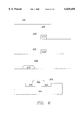
The low dielectric constant materials are polymerized into thin films of thicknesses of about 500 Å to about 5 μm on wafers for use in the manufacture of integrated circuits. FIG. 6 depicts a diagram of a multilevel integrated circuit chip 600 embodying the features of this invention. The substrate 604 has a source region 608, a drain region 612, and a polysilicon gate 616. A first interlevel dielectric (ILD) layer 620 overlays the substrate 600 and polysilicate gate 616. The wafer is subsequently planarized using chemical mechanical polishing another method known in the art. A floating polysilicon gate 624 is overlain by a second ILD layer 628. the wafer is again planarized, a first metal line 632 and a first intermetal dielectric (IMD) layer 636 are deposited. The wafer is again polished. On top of the IMD layer 636, a third metal line 640 and a second ILD layer 644 is deposited. The wafer is again planarized.
It should be appreciated by those of ordinary skill in the art that other embodiments may incorporate the concepts, methods, precursors, polymers, films, and devices of the above description and examples. The description and examples contained herein are not intended to limit the scope of the invention, but are included for illustration purposes only. It is to be understood that other embodiments of the invention can be developed and fall within the spirit and scope of the invention and claims.
Other features, aspects and objects of the invention can be obtained from a review of the figures and the claims.
Industrial Applicability
The invention includes novel precursors containing a fluorinated silane, fluorinated siloxane and fluorocarbons, each containing a fluorinated aromatic moiety. The precursors are suitable for making polymers with low dielectric constants and high thermal stability.
Additionally, the invention includes methods for making polymers for integrated circuit manufacture using novel fluorinated siloxanes, fluorocarbons, and fluorinated aromatic moieties.
Furthermore, the invention includes integrated circuits made using fluorinated siloxanes, fluorocarbons, or fluorinated aromatic moieties, with low dielectric constants.
According to the present invention, the polymers made from the disclosed precursors have low dielectric constant and high thermal stability. Therefore, integrated circuits made from these precursors have improved electrical and mechanical properties.

Claims (18)

What is claimed is:
1. A polymer made from a monomeric precursor using at least one method selected from the group consisting of transport polymerization and chemical vapor deposition the precursor selected from the group consisting of a fluorinated silane, a fluorinated siloxane and a fluorocarbon, said precursor comprising a fluorinated moiety with at least one of a sp2 C-F bond and hyperconjugated sp3 C-F bond.
2. The polymer of claim 1 wherein the precursor comprises (C6 H5-n Fn)m -SiH4-m wherein n is 1, 2, 3, 4, or 5, and wherein m is 1, 2, or 3.
3. The polymer of claim 1 wherein the precursor comprises (C6 H5-n Fn)m -Si(OCH3)4-m wherein n is 1, 2, 3, 4, or 5, and wherein m is 1, 2, or 3.
4. The polymer of claim 1 wherein the precursor comprises CH3-n Fn -C6 H4-p Fp --CH3-m Fm wherein n and m are 1, 2 or 3, and wherein p is 0, 1, 2, 3, or 4.
5. The polymer of claim 1 wherein the precursor comprises C6 F5 --CF3.
6. The polymer of claim 1 wherein the precursor comprises C6 F5 --CHF2.
7. The polymer of claim 1 wherein the precursor comprises C6 F5 --CH2 F.
8. The polymer of claim 1 wherein the precursor comprises C6 F5 --CH3.
9. The polymer of claim 1 wherein the precursor comprises C6 F5 --CF═CF2.
10. The polymer of claim 1 wherein the precursor comprises HCF2 --C6 F4 --CF2 H.
11. The polymer of claim 1 wherein the precursor comprises CH2 F--C6 F4 --CH2 F.
12. The polymer of claim 1 wherein the precursor comprises CF3 --C6 F4 --CF3.
13. The polymer of claim 1 wherein the precursor comprises CH3 --C6 F4 --CH3.
14. A rigid polymer having a dielectric constant below about 2.7, said polymer made from a monomeric precursor comprising a fluorinated aromatic moiety.
15. The polymer of claim 14 wherein the fluorinated aromatic moiety comprises a fluorinated phenyl moiety.
16. A rigid polymer having a dielectric constant below about 2.7, made from a monomeric precursor comprising at least a sp2 C-F bond.
17. The polymer as in claim 16 comprising sp2 C-F and hyperconjugated sp3 C-F bonds.
18. The polymer of claim 1, wherein precursor comprises (C6 H5-n Fn)--CH1-m Fm ═CH2-p FP, wherein n is 1, 2, 3, 4 or 5, wherein m is 0 or 1, and wherein p is 0, 1 or 2.
US08/957,481 1997-10-24 1997-10-24 Precursors for making low dielectric constant materials with improved thermal stability Expired - Fee Related US6020458A (en)

Priority Applications (7)

Application Number Priority Date Filing Date Title
US08/957,481 US6020458A (en) 1997-10-24 1997-10-24 Precursors for making low dielectric constant materials with improved thermal stability
KR1020007004416A KR100602222B1 (en) 1997-10-24 1998-10-15 Precursors for making low dielectric constant materials with improved thermal stability
AU10920/99A AU1092099A (en) 1997-10-24 1998-10-15 Precursors for making low dielectric constant materials with improved thermal stability
PCT/US1998/021840 WO1999021924A1 (en) 1997-10-24 1998-10-15 Precursors for making low dielectric constant materials with improved thermal stability
JP2000518023A JP2001521045A (en) 1997-10-24 1998-10-15 A precursor for making improved thermal equilibrium low dielectric constant materials
US09/440,297 US6258407B1 (en) 1997-10-24 1999-11-15 Precursors for making low dielectric constant materials with improved thermal stability
US09/836,815 US6534616B2 (en) 1997-10-24 2001-04-17 Precursors for making low dielectric constant materials with improved thermal stability

Applications Claiming Priority (1)

Application Number Priority Date Filing Date Title
US08/957,481 US6020458A (en) 1997-10-24 1997-10-24 Precursors for making low dielectric constant materials with improved thermal stability

Related Child Applications (1)

Application Number Title Priority Date Filing Date
US09/440,297 Division US6258407B1 (en) 1997-10-24 1999-11-15 Precursors for making low dielectric constant materials with improved thermal stability

Publications (1)

Publication Number Publication Date
US6020458A true US6020458A (en) 2000-02-01

Family

ID=25499624

Family Applications (3)

Application Number Title Priority Date Filing Date
US08/957,481 Expired - Fee Related US6020458A (en) 1997-10-24 1997-10-24 Precursors for making low dielectric constant materials with improved thermal stability
US09/440,297 Expired - Fee Related US6258407B1 (en) 1997-10-24 1999-11-15 Precursors for making low dielectric constant materials with improved thermal stability
US09/836,815 Expired - Fee Related US6534616B2 (en) 1997-10-24 2001-04-17 Precursors for making low dielectric constant materials with improved thermal stability

Family Applications After (2)

Application Number Title Priority Date Filing Date
US09/440,297 Expired - Fee Related US6258407B1 (en) 1997-10-24 1999-11-15 Precursors for making low dielectric constant materials with improved thermal stability
US09/836,815 Expired - Fee Related US6534616B2 (en) 1997-10-24 2001-04-17 Precursors for making low dielectric constant materials with improved thermal stability

Country Status (5)

Country Link
US (3) US6020458A (en)
JP (1) JP2001521045A (en)
KR (1) KR100602222B1 (en)
AU (1) AU1092099A (en)
WO (1) WO1999021924A1 (en)

Cited By (34)

* Cited by examiner, † Cited by third party
Publication number Priority date Publication date Assignee Title
US6331380B1 (en) * 1997-12-12 2001-12-18 Applied Materials, Inc. Method of pattern etching a low K dielectric layer
US6423384B1 (en) * 1999-06-25 2002-07-23 Applied Materials, Inc. HDP-CVD deposition of low dielectric constant amorphous carbon film
US20020119315A1 (en) * 2001-02-23 2002-08-29 Sheldon Aronowitz Process for forming a low dielectric constant fluorine and carbon-containing silicon oxide dielectric material characterized by improved resistance to oxidation
WO2002094906A1 (en) * 2001-05-23 2002-11-28 Nkt Research & Innovation A/S Method of plasma polymerisation of substituted benzenes, polymeric material obtainable by the method, and use thereof
US6559052B2 (en) 2000-07-07 2003-05-06 Applied Materials, Inc. Deposition of amorphous silicon films by high density plasma HDP-CVD at low temperatures
US6573030B1 (en) 2000-02-17 2003-06-03 Applied Materials, Inc. Method for depositing an amorphous carbon layer
US6583048B2 (en) 2001-01-17 2003-06-24 Air Products And Chemicals, Inc. Organosilicon precursors for interlayer dielectric films with low dielectric constants
US20030186477A1 (en) * 2002-03-29 2003-10-02 Applied Materials, Inc. Removable amorphous carbon CMP stop
US20030207750A1 (en) * 2001-02-23 2003-11-06 Vladimir Zubkov Low dielectric constant fluorine and carbon-containing silicon oxide dielectric material characterized by improved resistance to oxidation
US20030221621A1 (en) * 2000-04-21 2003-12-04 Applied Materials Inc. Method and apparatus for processing semiconductor substrates with hydroxyl radicals
US6660656B2 (en) * 1998-02-11 2003-12-09 Applied Materials Inc. Plasma processes for depositing low dielectric constant films
US6740601B2 (en) 2001-05-11 2004-05-25 Applied Materials Inc. HDP-CVD deposition process for filling high aspect ratio gaps
US20040101635A1 (en) * 2002-04-19 2004-05-27 Duerr Systems Gmbh Method and device for curing a coating
US20040149388A1 (en) * 2000-10-19 2004-08-05 Klaus Breitschwerdt Device and method for etching a substrate by using an inductively coupled plasma
US6777171B2 (en) 2001-04-20 2004-08-17 Applied Materials, Inc. Fluorine-containing layers for damascene structures
US20040161617A1 (en) * 2000-02-08 2004-08-19 Todd Michael A. Process for depositing low dielectric constant materials
US6825303B2 (en) 2001-02-26 2004-11-30 Dielectric Systems, Inc. Integration of low ε thin films and Ta into Cu dual damascene
US20040255862A1 (en) * 2001-02-26 2004-12-23 Lee Chung J. Reactor for producing reactive intermediates for low dielectric constant polymer thin films
US20050025681A1 (en) * 1998-10-20 2005-02-03 Radiant Technology Corporation UV-enhanced, in-line, infrared phosphorous diffusion furnace
US7015168B2 (en) 2001-02-23 2006-03-21 Lsi Logic Corporation Low dielectric constant fluorine and carbon-containing silicon oxide dielectric material characterized by improved resistance to oxidation
US20060201426A1 (en) * 2004-05-25 2006-09-14 Lee Chung J Reactor for Producing Reactive Intermediates for Transport Polymerization
US20060274474A1 (en) * 2005-06-01 2006-12-07 Lee Chung J Substrate Holder
US20070098890A1 (en) * 2003-09-17 2007-05-03 Masaru Sasaki Fabrication of low dielectric constant insulating film
US20080011332A1 (en) * 2002-04-26 2008-01-17 Accretech Usa, Inc. Method and apparatus for cleaning a wafer substrate
US20080017316A1 (en) * 2002-04-26 2008-01-24 Accretech Usa, Inc. Clean ignition system for wafer substrate processing
US20080190558A1 (en) * 2002-04-26 2008-08-14 Accretech Usa, Inc. Wafer processing apparatus and method
US20080254233A1 (en) * 2007-04-10 2008-10-16 Kwangduk Douglas Lee Plasma-induced charge damage control for plasma enhanced chemical vapor deposition processes
US7514375B1 (en) * 2006-08-08 2009-04-07 Novellus Systems, Inc. Pulsed bias having high pulse frequency for filling gaps with dielectric material
US20100075507A1 (en) * 2008-09-22 2010-03-25 Taiwan Semiconductor Manufacturing Company, Ltd. Method of Fabricating a Gate Dielectric for High-K Metal Gate Devices
US7749863B1 (en) * 2005-05-12 2010-07-06 Hrl Laboratories, Llc Thermal management substrates
US20110056513A1 (en) * 2008-06-05 2011-03-10 Axel Hombach Method for treating surfaces, lamp for said method, and irradiation system having said lamp
US20120031559A1 (en) * 2010-08-04 2012-02-09 Lam Research Corporation Dual Plasma Volume Processing Apparatus for Neutral/Ion Flux Control
US8869742B2 (en) 2010-08-04 2014-10-28 Lam Research Corporation Plasma processing chamber with dual axial gas injection and exhaust
US9093265B2 (en) * 2013-10-15 2015-07-28 Taiwan Semiconductor Manufacturing Co., Ltd. High UV curing efficiency for low-k dielectrics

Families Citing this family (47)

* Cited by examiner, † Cited by third party
Publication number Priority date Publication date Assignee Title
JP3469761B2 (en) * 1997-10-30 2003-11-25 東京エレクトロン株式会社 Method for manufacturing semiconductor device
TW430882B (en) * 1997-11-20 2001-04-21 Tokyo Electron Ltd Plasma film forming method
US6593247B1 (en) * 1998-02-11 2003-07-15 Applied Materials, Inc. Method of depositing low k films using an oxidizing plasma
US6936310B1 (en) * 1999-04-02 2005-08-30 Sharp Kabushiki Kaisha Plasma processing method
US6475930B1 (en) * 2000-01-31 2002-11-05 Motorola, Inc. UV cure process and tool for low k film formation
JP2001267310A (en) * 2000-03-17 2001-09-28 Tokyo Electron Ltd Method and device for film forming plasma
JP2002009152A (en) * 2000-06-21 2002-01-11 Nec Corp Semiconductor device and its manufacturing method
JP2002075980A (en) * 2000-08-30 2002-03-15 Miyazaki Oki Electric Co Ltd Method for depositing low dielectric film by vacuum ultraviolet cvd
US6436822B1 (en) * 2000-11-20 2002-08-20 Intel Corporation Method for making a carbon doped oxide dielectric material
US6797343B2 (en) 2001-12-20 2004-09-28 Dielectric Systems, Inc. Dielectric thin films from fluorinated precursors
US7192645B2 (en) 2001-02-26 2007-03-20 Dielectric Systems, Inc. Porous low E (<2.0) thin films by transport co-polymerization
US20030196680A1 (en) * 2002-04-19 2003-10-23 Dielectric Systems, Inc Process modules for transport polymerization of low epsilon thin films
US7026052B2 (en) 2001-02-26 2006-04-11 Dielectric Systems, Inc. Porous low k(<2.0) thin film derived from homo-transport-polymerization
US20040055539A1 (en) * 2002-09-13 2004-03-25 Dielectric Systems, Inc. Reactive-reactor for generation of gaseous intermediates
US6881447B2 (en) 2002-04-04 2005-04-19 Dielectric Systems, Inc. Chemically and electrically stabilized polymer films
US6605549B2 (en) * 2001-09-29 2003-08-12 Intel Corporation Method for improving nucleation and adhesion of CVD and ALD films deposited onto low-dielectric-constant dielectrics
EP1448807A4 (en) * 2001-10-30 2005-07-13 Massachusetts Inst Technology Fluorocarbon-organosilicon copolymers and coatings prepared by hot-filament chemical vapor deposition
EP1463740A2 (en) 2002-01-08 2004-10-06 Silecs, Inc. Materials and methods for forming hybrid organic-inorganic dielectric materials
TWI236505B (en) * 2002-01-14 2005-07-21 Nat Science Council Thermal cracking chemical vapor deposition process for nanocarbonaceous material
DE10237787A1 (en) * 2002-08-17 2004-03-04 Robert Bosch Gmbh Layer system with a silicon layer and a passivation layer, method for producing a passivation layer on a silicon layer and their use
US7404990B2 (en) 2002-11-14 2008-07-29 Air Products And Chemicals, Inc. Non-thermal process for forming porous low dielectric constant films
TWI240959B (en) 2003-03-04 2005-10-01 Air Prod & Chem Mechanical enhancement of dense and porous organosilicate materials by UV exposure
US8865271B2 (en) * 2003-06-06 2014-10-21 Neophotonics Corporation High rate deposition for the formation of high quality optical coatings
US7138180B2 (en) * 2003-10-16 2006-11-21 Wisconsin Alumni Research Foundation Hard carbon films formed from plasma treated polymer surfaces
US6962871B2 (en) 2004-03-31 2005-11-08 Dielectric Systems, Inc. Composite polymer dielectric film
US7094661B2 (en) 2004-03-31 2006-08-22 Dielectric Systems, Inc. Single and dual damascene techniques utilizing composite polymer dielectric film
US7309395B2 (en) 2004-03-31 2007-12-18 Dielectric Systems, Inc. System for forming composite polymer dielectric film
US20050245693A1 (en) * 2004-05-03 2005-11-03 Bhatt Sanjiv M Fluorinated aromatic polymers
DE102005003806B3 (en) * 2005-01-26 2006-07-20 Thermo Electron (Bremen) Gmbh Glow discharge source for analysis of solid sample by means of glow discharge has anode and cathode and by means of direct and indirect cooling of sample and cooling agent provide at least one peltier-element
US20070299176A1 (en) * 2005-01-28 2007-12-27 Markley Thomas J Photodefinable low dielectric constant material and method for making and using same
US7867779B2 (en) 2005-02-03 2011-01-11 Air Products And Chemicals, Inc. System and method comprising same for measurement and/or analysis of particles in gas stream
US20060183055A1 (en) * 2005-02-15 2006-08-17 O'neill Mark L Method for defining a feature on a substrate
US7425350B2 (en) * 2005-04-29 2008-09-16 Asm Japan K.K. Apparatus, precursors and deposition methods for silicon-containing materials
US7549905B2 (en) 2005-09-30 2009-06-23 International Display Systems, Inc. Method of encapsulating an organic light emitting device
US8945684B2 (en) * 2005-11-04 2015-02-03 Essilor International (Compagnie Generale D'optique) Process for coating an article with an anti-fouling surface coating by vacuum evaporation
US7621794B2 (en) 2005-11-09 2009-11-24 International Display Systems, Inc. Method of encapsulating an organic light-emitting device
US20070264842A1 (en) * 2006-05-12 2007-11-15 Samsung Electronics Co., Ltd. Insulation film deposition method for a semiconductor device
US20070299239A1 (en) * 2006-06-27 2007-12-27 Air Products And Chemicals, Inc. Curing Dielectric Films Under A Reducing Atmosphere
US20080012074A1 (en) * 2006-07-14 2008-01-17 Air Products And Chemicals, Inc. Low Temperature Sol-Gel Silicates As Dielectrics or Planarization Layers For Thin Film Transistors
US20080264672A1 (en) * 2007-04-26 2008-10-30 Air Products And Chemicals, Inc. Photoimprintable Low Dielectric Constant Material and Method for Making and Using Same
US20090096106A1 (en) 2007-10-12 2009-04-16 Air Products And Chemicals, Inc. Antireflective coatings
US8987039B2 (en) 2007-10-12 2015-03-24 Air Products And Chemicals, Inc. Antireflective coatings for photovoltaic applications
JP5501807B2 (en) * 2009-03-31 2014-05-28 東京エレクトロン株式会社 Processing equipment
TWI423331B (en) * 2009-06-26 2014-01-11 Tokyo Electron Ltd Plasma treatment method
FR2950080B1 (en) * 2009-09-17 2012-03-02 Essilor Int METHOD AND DEVICE FOR GAS PHASE CHEMICAL DEPOSITION OF A POLYMER FILM ON A SUBSTRATE
CN103105736A (en) * 2011-11-11 2013-05-15 中芯国际集成电路制造(上海)有限公司 Photolithography method and etching method
CN109354903B (en) * 2018-10-24 2020-01-17 江苏菲沃泰纳米科技有限公司 High-transparency low-chromatic-aberration nano coating and preparation method thereof

Citations (26)

* Cited by examiner, † Cited by third party
Publication number Priority date Publication date Assignee Title
US3440277A (en) * 1965-12-13 1969-04-22 Us Air Force Fluoroaromatic compounds
US4291244A (en) * 1979-09-04 1981-09-22 Union Carbide Corporation Electrets
JPS60231442A (en) * 1984-04-28 1985-11-18 Toyota Central Res & Dev Lab Inc Water-repellent glass
US5139813A (en) * 1990-09-28 1992-08-18 Union Carbide Chemicals & Plastics Technology Corporation Method for inducing fluorescence in parylene films by an active plasma
US5210341A (en) * 1991-12-20 1993-05-11 Union Carbide Chemicals & Plastics Technology Corporation Processes for the preparation of octafluoro-[2,2]paracyclophane
US5268202A (en) * 1992-10-09 1993-12-07 Rensselaer Polytechnic Institute Vapor deposition of parylene-F using 1,4-bis (trifluoromethyl) benzene
US5324813A (en) * 1992-07-22 1994-06-28 International Business Machines Corporation Low dielectric constant fluorinated polymers and methods of fabrication thereof
US5334454A (en) * 1991-07-22 1994-08-02 Dow Corning Corporation Articles by plasma-activated chemical vapor deposition of fluorinated cyclic siloxanes
US5424097A (en) * 1993-09-30 1995-06-13 Specialty Coating Systems, Inc. Continuous vapor deposition apparatus
US5534068A (en) * 1995-10-27 1996-07-09 Specialty Coating Systems, Inc. Parylene deposition apparatus including a tapered deposition chamber and dual vacuum outlet pumping arrangement
US5536321A (en) * 1995-10-27 1996-07-16 Specialty Coating Systems, Inc. Parylene deposition apparatus including a post-pyrolysis filtering chamber and a deposition chamber inlet filter
US5536319A (en) * 1995-10-27 1996-07-16 Specialty Coating Systems, Inc. Parylene deposition apparatus including an atmospheric shroud and inert gas source
US5536892A (en) * 1995-10-18 1996-07-16 Specialty Coating Systems, Inc. Processes for the preparation of octafluoro-[2,2]paracyclophane
US5536317A (en) * 1995-10-27 1996-07-16 Specialty Coating Systems, Inc. Parylene deposition apparatus including a quartz crystal thickness/rate controller
US5536322A (en) * 1995-10-27 1996-07-16 Specialty Coating Systems, Inc. Parylene deposition apparatus including a heated and cooled support platen and an electrostatic clamping device
US5538758A (en) * 1995-10-27 1996-07-23 Specialty Coating Systems, Inc. Method and apparatus for the deposition of parylene AF4 onto semiconductor wafers
US5556473A (en) * 1995-10-27 1996-09-17 Specialty Coating Systems, Inc. Parylene deposition apparatus including dry vacuum pump system and downstream cold trap
EP0769788A2 (en) * 1995-10-20 1997-04-23 W.L. Gore & Associates, Inc. Low dielectric constant material for use as an insulation element in an electronic device
WO1997014666A1 (en) * 1995-10-18 1997-04-24 Specialty Coating Systems, Inc. Processes for the preparation of octafluoro-[2,2]paracyclophane
WO1997015699A2 (en) * 1995-10-27 1997-05-01 Specialty Coating Systems, Inc. Method and apparatus for the deposition of parylene af4 onto semiconductor wafers
WO1997015951A1 (en) * 1995-10-27 1997-05-01 Specialty Coating Systems, Inc. Parylene polymer layers
US5637395A (en) * 1984-03-12 1997-06-10 Nitto Electric Industrial Co., Ltd. Thin adhesive sheet for working semiconductor wafers
US5708116A (en) * 1995-05-31 1998-01-13 The United States Of America As Represented By The Secretary Of The Navy Low dielectric constant allylics
WO1998024743A1 (en) * 1996-12-06 1998-06-11 Speciality Coating Systems, Inc. Tfpx synthesis
US5783614A (en) * 1997-02-21 1998-07-21 Copytele, Inc. Polymeric-coated dielectric particles and formulation and method for preparing same
WO1998041490A1 (en) * 1997-03-14 1998-09-24 Specialty Coating Systems, Inc. Af4 synthesis

Family Cites Families (16)

* Cited by examiner, † Cited by third party
Publication number Priority date Publication date Assignee Title
US3332891A (en) 1963-09-23 1967-07-25 Union Carbide Corp Process for the preparation of alpha-per-fluoro-p-xylylene polymers
US3274267A (en) 1963-09-23 1966-09-20 Union Carbide Corp Cyclic alpha-perfluoro-di-p-xylylenes
US3342754A (en) 1966-02-18 1967-09-19 Union Carbide Corp Para-xylylene polymers
US4737379A (en) 1982-09-24 1988-04-12 Energy Conversion Devices, Inc. Plasma deposited coatings, and low temperature plasma method of making same
DE3240303C1 (en) 1982-10-30 1984-01-19 Merck Patent Gmbh, 6100 Darmstadt Process for the preparation of [2,2] -paracyclophane
JPS601846A (en) 1983-06-18 1985-01-08 Toshiba Corp Multilayer interconnection structure semiconductor device and manufacture thereof
US4657777A (en) * 1984-12-17 1987-04-14 Canon Kabushiki Kaisha Formation of deposited film
US4911992A (en) 1986-12-04 1990-03-27 Dow Corning Corporation Platinum or rhodium catalyzed multilayer ceramic coatings from hydrogen silsesquioxane resin and metal oxides
JP3407086B2 (en) 1994-06-17 2003-05-19 日本テキサス・インスツルメンツ株式会社 Method for manufacturing semiconductor device
AU5674096A (en) 1995-05-05 1996-11-21 Specialty Coating Systems, Inc. Flat panel display with parylene barrier and protective film s
CN1089281C (en) 1996-10-25 2002-08-21 特殊涂覆系统公司 Processf or making a parylene coating
US5759906A (en) 1997-04-11 1998-06-02 Industrial Technology Research Institute Planarization method for intermetal dielectrics between multilevel interconnections on integrated circuits
US6051321A (en) * 1997-10-24 2000-04-18 Quester Technology, Inc. Low dielectric constant materials and method
TW522144B (en) * 1998-01-20 2003-03-01 Nippon Catalytic Chem Ind Process for production of 1,4-bis(difluoroalkyl) benzene derivative
US6184572B1 (en) * 1998-04-29 2001-02-06 Novellus Systems, Inc. Interlevel dielectric stack containing plasma deposited fluorinated amorphous carbon films for semiconductor devices
EP1123991A3 (en) * 2000-02-08 2002-11-13 Asm Japan K.K. Low dielectric constant materials and processes

Patent Citations (26)

* Cited by examiner, † Cited by third party
Publication number Priority date Publication date Assignee Title
US3440277A (en) * 1965-12-13 1969-04-22 Us Air Force Fluoroaromatic compounds
US4291244A (en) * 1979-09-04 1981-09-22 Union Carbide Corporation Electrets
US5637395A (en) * 1984-03-12 1997-06-10 Nitto Electric Industrial Co., Ltd. Thin adhesive sheet for working semiconductor wafers
JPS60231442A (en) * 1984-04-28 1985-11-18 Toyota Central Res & Dev Lab Inc Water-repellent glass
US5139813A (en) * 1990-09-28 1992-08-18 Union Carbide Chemicals & Plastics Technology Corporation Method for inducing fluorescence in parylene films by an active plasma
US5334454A (en) * 1991-07-22 1994-08-02 Dow Corning Corporation Articles by plasma-activated chemical vapor deposition of fluorinated cyclic siloxanes
US5210341A (en) * 1991-12-20 1993-05-11 Union Carbide Chemicals & Plastics Technology Corporation Processes for the preparation of octafluoro-[2,2]paracyclophane
US5324813A (en) * 1992-07-22 1994-06-28 International Business Machines Corporation Low dielectric constant fluorinated polymers and methods of fabrication thereof
US5268202A (en) * 1992-10-09 1993-12-07 Rensselaer Polytechnic Institute Vapor deposition of parylene-F using 1,4-bis (trifluoromethyl) benzene
US5424097A (en) * 1993-09-30 1995-06-13 Specialty Coating Systems, Inc. Continuous vapor deposition apparatus
US5708116A (en) * 1995-05-31 1998-01-13 The United States Of America As Represented By The Secretary Of The Navy Low dielectric constant allylics
US5536892A (en) * 1995-10-18 1996-07-16 Specialty Coating Systems, Inc. Processes for the preparation of octafluoro-[2,2]paracyclophane
WO1997014666A1 (en) * 1995-10-18 1997-04-24 Specialty Coating Systems, Inc. Processes for the preparation of octafluoro-[2,2]paracyclophane
EP0769788A2 (en) * 1995-10-20 1997-04-23 W.L. Gore & Associates, Inc. Low dielectric constant material for use as an insulation element in an electronic device
US5538758A (en) * 1995-10-27 1996-07-23 Specialty Coating Systems, Inc. Method and apparatus for the deposition of parylene AF4 onto semiconductor wafers
US5536319A (en) * 1995-10-27 1996-07-16 Specialty Coating Systems, Inc. Parylene deposition apparatus including an atmospheric shroud and inert gas source
US5556473A (en) * 1995-10-27 1996-09-17 Specialty Coating Systems, Inc. Parylene deposition apparatus including dry vacuum pump system and downstream cold trap
US5536322A (en) * 1995-10-27 1996-07-16 Specialty Coating Systems, Inc. Parylene deposition apparatus including a heated and cooled support platen and an electrostatic clamping device
US5536317A (en) * 1995-10-27 1996-07-16 Specialty Coating Systems, Inc. Parylene deposition apparatus including a quartz crystal thickness/rate controller
WO1997015699A2 (en) * 1995-10-27 1997-05-01 Specialty Coating Systems, Inc. Method and apparatus for the deposition of parylene af4 onto semiconductor wafers
WO1997015951A1 (en) * 1995-10-27 1997-05-01 Specialty Coating Systems, Inc. Parylene polymer layers
US5536321A (en) * 1995-10-27 1996-07-16 Specialty Coating Systems, Inc. Parylene deposition apparatus including a post-pyrolysis filtering chamber and a deposition chamber inlet filter
US5534068A (en) * 1995-10-27 1996-07-09 Specialty Coating Systems, Inc. Parylene deposition apparatus including a tapered deposition chamber and dual vacuum outlet pumping arrangement
WO1998024743A1 (en) * 1996-12-06 1998-06-11 Speciality Coating Systems, Inc. Tfpx synthesis
US5783614A (en) * 1997-02-21 1998-07-21 Copytele, Inc. Polymeric-coated dielectric particles and formulation and method for preparing same
WO1998041490A1 (en) * 1997-03-14 1998-09-24 Specialty Coating Systems, Inc. Af4 synthesis

Non-Patent Citations (27)

* Cited by examiner, † Cited by third party
Title
Hacker, Organic and Inorganic Spin on Polymers for Low Dielectric Constant Applications, MRS Bulletin, 38 77, Oct. 1997. *
Hacker, Organic and Inorganic Spin-on Polymers for Low-Dielectric-Constant Applications, MRS Bulletin, 38-77, Oct. 1997.
High Vacuum Electrical Feedthroughs Within Easy Reach, MDC Vacuum Products Corporation, Circle No. 12 on Reader Service Card. *
J.I. Krochiwitz, Encyclopedia of Chem. Tech., vol. 5, 320 373, 1991. *
J.I. Krochiwitz, Encyclopedia of Chem. Tech., vol. 5, 320-373, 1991.
J.J. McKetta, Encyclopedia of Chem. Proc. & Design, vol. 14, 276 291, 1992. *
J.J. McKetta, Encyclopedia of Chem. Proc. & Design, vol. 14, 276-291, 1992.
Jozef Bicerano, Prediction of Polymer Properties , Second Edition, Marcel Dekker, Inc., pp. 1 15, 50 61, 108 111, and 280 295, (1996). *
Jozef Bicerano, Prediction of Polymer Properties, Second Edition, Marcel Dekker, Inc., pp. 1-15, 50-61, 108-111, and 280-295, (1996).
Labelle, et al., Characterization of Pulsed Plasma Enhanced Chemical Vapor Deposited Fluorocarbon Thin Films, Feb. 10 11, 1997, DUMIC Conference, 1997 ISMIC 222D/97/0098, 98 105. *
Labelle, et al., Characterization of Pulsed-Plasma Enhanced Chemical Vapor Deposited Fluorocarbon Thin Films, Feb. 10-11, 1997, DUMIC Conference, 1997 ISMIC--222D/97/0098, 98-105.
Lee, et al., Low Dielectric Constant materials for ULSI Interlayer Dielectric Applications, MRS Bulletin, 19 27, Oct. 1997. *
Lee, et al., Low-Dielectric Constant materials for ULSI Interlayer-Dielectric Applications, MRS Bulletin, 19-27, Oct. 1997.
Lee, Transport Polymerization of Gaseous Intermediates and Polymer Crystals Growth, J. Macromol. Sci. Rev. Macromol. Chem., C16(1), 79 127 (1977 1978). *
Lee, Transport Polymerization of Gaseous Intermediates and Polymer Crystals Growth, J. Macromol. Sci. --Rev. Macromol. Chem., C16(1), 79-127 (1977-1978).
Lu, et al., Vapor Deposition of Low Dielectric Constant Polymeric Thin Films, MRS Bulletin, 28 31, Oct. 1997. *
Lu, et al., Vapor Deposition of Low-Dielectric-Constant Polymeric Thin Films, MRS Bulletin, 28-31, Oct. 1997.
McClatchie, et al., Low Dielectric Constant Flowfill Technology for IMD Applications, Feb. 10 11, 1997,DUMIC Conference, 1997 ISMIC 222D/97/0034, 34 40. *
McClatchie, et al., Low Dielectric Constant Flowfill Technology for IMD Applications, Feb. 10-11, 1997,DUMIC Conference, 1997 ISMIC--222D/97/0034, 34-40.
Meriaudeau, et al., Dehydrocyclization of Alkanes Over Zeolite Supported Metal Catalysts: Monofunctional or Bifunctional Route, Catal. Rev. Sci. Eng., 39 (1&2), 5 48, 1997. *
Meriaudeau, et al., Dehydrocyclization of Alkanes Over Zeolite-Supported Metal Catalysts: Monofunctional or Bifunctional Route, Catal. Rev. Sci. Eng., 39 (1&2), 5-48, 1997.
Robles, et al., Characterization of High Density Plasma Chemical Vapor Deposited Carbon and Fluorinated Carbon Films for Ultra Low Dielectric Applications, Feb. 10 11, 1997, DUMIC Conference, 1997 ISMIC 222D/97/0026, 26 33. *
Robles, et al., Characterization of High Density Plasma Chemical Vapor Deposited α-Carbon and α-Fluorinated Carbon Films for Ultra Low Dielectric Applications, Feb. 10-11, 1997, DUMIC Conference, 1997 ISMIC--222D/97/0026, 26-33.
Shimogaki, et al., How Low Dielectric Constant of F Doped SiO 2 Films Can be Obtained, Feb. 10 11, 1997, DUMIC Conference, 1997 ISMIC222D/97/0034, 189 196. *
Shimogaki, et al., How Low Dielectric Constant of F-Doped SiO2 Films Can be Obtained, Feb. 10-11, 1997, DUMIC Conference, 1997 ISMIC222D/97/0034, 189-196.
Sugahara, et al., Low Dielectric Constant Carbon Containing SiO 2 Films Deposited by PECVD Technique Using a Novel CVD Precursor, Feb. 10 11, 1997, DUMIC Conference, 1997 ISMIC 222D/97/0019, 19 25. *
Sugahara, et al., Low Dielectric Constant Carbon Containing SiO2 Films Deposited by PECVD Technique Using a Novel CVD Precursor, Feb. 10-11, 1997, DUMIC Conference, 1997 ISMIC--222D/97/0019, 19-25.

Cited By (57)

* Cited by examiner, † Cited by third party
Publication number Priority date Publication date Assignee Title
US6331380B1 (en) * 1997-12-12 2001-12-18 Applied Materials, Inc. Method of pattern etching a low K dielectric layer
US6660656B2 (en) * 1998-02-11 2003-12-09 Applied Materials Inc. Plasma processes for depositing low dielectric constant films
US20050025681A1 (en) * 1998-10-20 2005-02-03 Radiant Technology Corporation UV-enhanced, in-line, infrared phosphorous diffusion furnace
US6423384B1 (en) * 1999-06-25 2002-07-23 Applied Materials, Inc. HDP-CVD deposition of low dielectric constant amorphous carbon film
US20070032676A1 (en) * 2000-02-08 2007-02-08 Todd Michael A Process for depositing low dielectric constant materials
US7144620B2 (en) * 2000-02-08 2006-12-05 Asm Japan K.K. Process for depositing low dielectric constant materials
US20040161617A1 (en) * 2000-02-08 2004-08-19 Todd Michael A. Process for depositing low dielectric constant materials
US7544827B2 (en) 2000-02-08 2009-06-09 Asm Japan K.K. Process for depositing low dielectric constant materials
US7335462B2 (en) 2000-02-17 2008-02-26 Applied Materials, Inc. Method of depositing an amorphous carbon layer
US6573030B1 (en) 2000-02-17 2003-06-03 Applied Materials, Inc. Method for depositing an amorphous carbon layer
US6841341B2 (en) 2000-02-17 2005-01-11 Applied Materials, Inc. Method of depositing an amorphous carbon layer
US20050112509A1 (en) * 2000-02-17 2005-05-26 Kevin Fairbairn Method of depositing an amrphous carbon layer
US20070128538A1 (en) * 2000-02-17 2007-06-07 Applied Materials, Inc. Method of depositing an amorphous carbon layer
US7223526B2 (en) 2000-02-17 2007-05-29 Applied Materials, Inc. Method of depositing an amorphous carbon layer
US20030221621A1 (en) * 2000-04-21 2003-12-04 Applied Materials Inc. Method and apparatus for processing semiconductor substrates with hydroxyl radicals
US6559052B2 (en) 2000-07-07 2003-05-06 Applied Materials, Inc. Deposition of amorphous silicon films by high density plasma HDP-CVD at low temperatures
US20040149388A1 (en) * 2000-10-19 2004-08-05 Klaus Breitschwerdt Device and method for etching a substrate by using an inductively coupled plasma
US6583048B2 (en) 2001-01-17 2003-06-24 Air Products And Chemicals, Inc. Organosilicon precursors for interlayer dielectric films with low dielectric constants
US20030207750A1 (en) * 2001-02-23 2003-11-06 Vladimir Zubkov Low dielectric constant fluorine and carbon-containing silicon oxide dielectric material characterized by improved resistance to oxidation
US7015168B2 (en) 2001-02-23 2006-03-21 Lsi Logic Corporation Low dielectric constant fluorine and carbon-containing silicon oxide dielectric material characterized by improved resistance to oxidation
US20020119315A1 (en) * 2001-02-23 2002-08-29 Sheldon Aronowitz Process for forming a low dielectric constant fluorine and carbon-containing silicon oxide dielectric material characterized by improved resistance to oxidation
US6858195B2 (en) * 2001-02-23 2005-02-22 Lsi Logic Corporation Process for forming a low dielectric constant fluorine and carbon-containing silicon oxide dielectric material
US20040255862A1 (en) * 2001-02-26 2004-12-23 Lee Chung J. Reactor for producing reactive intermediates for low dielectric constant polymer thin films
US6825303B2 (en) 2001-02-26 2004-11-30 Dielectric Systems, Inc. Integration of low ε thin films and Ta into Cu dual damascene
US20050000435A1 (en) * 2001-02-26 2005-01-06 Lee Chung J. Reactor for producing reactive intermediates for low dielectric constant polymer thin films
US6777171B2 (en) 2001-04-20 2004-08-17 Applied Materials, Inc. Fluorine-containing layers for damascene structures
US6914016B2 (en) 2001-05-11 2005-07-05 Applied Materials, Inc. HDP-CVD deposition process for filling high aspect ratio gaps
US6740601B2 (en) 2001-05-11 2004-05-25 Applied Materials Inc. HDP-CVD deposition process for filling high aspect ratio gaps
US20050181632A1 (en) * 2001-05-11 2005-08-18 Applied Materials, Inc., A Delaware Corporation HDP-CVD deposition process for filling high aspect ratio gaps
US7196021B2 (en) 2001-05-11 2007-03-27 Applied Materials, Inc. HDP-CVD deposition process for filling high aspect ratio gaps
WO2002094906A1 (en) * 2001-05-23 2002-11-28 Nkt Research & Innovation A/S Method of plasma polymerisation of substituted benzenes, polymeric material obtainable by the method, and use thereof
US20040202880A1 (en) * 2001-05-23 2004-10-14 Bjorn Winther-Jensen Method of plasma polymerisation of substituted benzenes, polymeric material obtainable by the method, and use thereof
US20050191848A1 (en) * 2002-03-29 2005-09-01 Bencher Christopher D. Removable amorphous carbon CMP stop
US20070054500A1 (en) * 2002-03-29 2007-03-08 Applied Materials, Inc. Removable amorphous carbon cmp stop
US20030186477A1 (en) * 2002-03-29 2003-10-02 Applied Materials, Inc. Removable amorphous carbon CMP stop
US7507677B2 (en) 2002-03-29 2009-03-24 Applied Materials, Inc. Removable amorphous carbon CMP stop
US6852647B2 (en) 2002-03-29 2005-02-08 Applied Materials, Inc. Removable amorphous carbon CMP stop
US7148156B2 (en) 2002-03-29 2006-12-12 Applied Materials, Inc. Removable amorphous carbon CMP stop
US20040101635A1 (en) * 2002-04-19 2004-05-27 Duerr Systems Gmbh Method and device for curing a coating
US7488518B2 (en) * 2002-04-19 2009-02-10 Duerr Systems Gmbh Method and device for curing a coating
US20080011332A1 (en) * 2002-04-26 2008-01-17 Accretech Usa, Inc. Method and apparatus for cleaning a wafer substrate
US20080190558A1 (en) * 2002-04-26 2008-08-14 Accretech Usa, Inc. Wafer processing apparatus and method
US20080017316A1 (en) * 2002-04-26 2008-01-24 Accretech Usa, Inc. Clean ignition system for wafer substrate processing
US20070098890A1 (en) * 2003-09-17 2007-05-03 Masaru Sasaki Fabrication of low dielectric constant insulating film
US7645481B2 (en) * 2003-09-17 2010-01-12 Tokyo Electron Limited Fabrication of low dielectric constant insulating film
US20060201426A1 (en) * 2004-05-25 2006-09-14 Lee Chung J Reactor for Producing Reactive Intermediates for Transport Polymerization
US7749863B1 (en) * 2005-05-12 2010-07-06 Hrl Laboratories, Llc Thermal management substrates
US20060274474A1 (en) * 2005-06-01 2006-12-07 Lee Chung J Substrate Holder
US7514375B1 (en) * 2006-08-08 2009-04-07 Novellus Systems, Inc. Pulsed bias having high pulse frequency for filling gaps with dielectric material
US20080254233A1 (en) * 2007-04-10 2008-10-16 Kwangduk Douglas Lee Plasma-induced charge damage control for plasma enhanced chemical vapor deposition processes
US20110056513A1 (en) * 2008-06-05 2011-03-10 Axel Hombach Method for treating surfaces, lamp for said method, and irradiation system having said lamp
US20100075507A1 (en) * 2008-09-22 2010-03-25 Taiwan Semiconductor Manufacturing Company, Ltd. Method of Fabricating a Gate Dielectric for High-K Metal Gate Devices
US9711373B2 (en) * 2008-09-22 2017-07-18 Taiwan Semiconductor Manufacturing Company, Ltd. Method of fabricating a gate dielectric for high-k metal gate devices
US20120031559A1 (en) * 2010-08-04 2012-02-09 Lam Research Corporation Dual Plasma Volume Processing Apparatus for Neutral/Ion Flux Control
US8869742B2 (en) 2010-08-04 2014-10-28 Lam Research Corporation Plasma processing chamber with dual axial gas injection and exhaust
US9184028B2 (en) * 2010-08-04 2015-11-10 Lam Research Corporation Dual plasma volume processing apparatus for neutral/ion flux control
US9093265B2 (en) * 2013-10-15 2015-07-28 Taiwan Semiconductor Manufacturing Co., Ltd. High UV curing efficiency for low-k dielectrics

Also Published As

Publication number Publication date
KR20010031399A (en) 2001-04-16
US20010029110A1 (en) 2001-10-11
JP2001521045A (en) 2001-11-06
US6534616B2 (en) 2003-03-18
AU1092099A (en) 1999-05-17
US6258407B1 (en) 2001-07-10
WO1999021924A1 (en) 1999-05-06
KR100602222B1 (en) 2006-07-19

Similar Documents

Publication Publication Date Title
US6020458A (en) Precursors for making low dielectric constant materials with improved thermal stability
US6086679A (en) Deposition systems and processes for transport polymerization and chemical vapor deposition
US6140456A (en) Chemicals and processes for making fluorinated poly(para-xylylenes)
US6051321A (en) Low dielectric constant materials and method
KR100767246B1 (en) Method for enhancing deposition rate of chemical vapor deposition films
CN1938833B (en) Techniques promoting adhesion of porous low k film to underlying barrier layer and interconnection structure
US20020160626A1 (en) Siloxan polymer film on semiconductor substrate
EP1342809A1 (en) Method of forming a low dialectric constant insulation film
US20080153311A1 (en) Method for depositing an amorphous carbon film with improved density and step coverage
US20120208373A1 (en) Method for depositing an amorphous carbon film with improved density and step coverage
US20040038514A1 (en) Method for forming low-k hard film
KR100899726B1 (en) Method of improving initiation layer for low-k dielectric film by digital liquid flow meter
JP5785152B2 (en) Chemical vapor deposition
US6784123B2 (en) Insulation film on semiconductor substrate and method for forming same
WO2001036703A1 (en) System and method for depositing inorganic/organic dielectric films
US20110313184A1 (en) Insulating film material, and film formation method utilizing the material, and insulating film
US6323297B1 (en) Low dielectric constant materials with improved thermal and mechanical properties
KR100494194B1 (en) Porogens, porogenated precursors and methods for using the same to provide porous organosilica glass films with low dielectric constants
US20060105581A1 (en) Glycol doping agents in carbon doped oxide films
JP3781730B2 (en) Method for forming silicon insulating film having low dielectric constant and high mechanical strength
KR20220061162A (en) Monoalkoxysilane and high-density organosilica film prepared therefrom
JP4651076B2 (en) Method for forming an insulating film on a semiconductor substrate

Legal Events

Date Code Title Description
AS Assignment

Owner name: QUESTER TECHNOLOGY, INC., CALIFORNIA

Free format text: ASSIGNMENT OF ASSIGNORS INTEREST;ASSIGNORS:LEE, CHUNG;WANG, HUI;FOGGIATO, GIOVANNI ANTONIO;REEL/FRAME:008889/0024

Effective date: 19971023

AS Assignment

Owner name: CANON U.S.A., INC., NEW YORK

Free format text: ASSIGNMENT OF ASSIGNORS INTEREST;ASSIGNOR:QUESTER TECHNOLOGY, INC.;REEL/FRAME:013835/0049

Effective date: 20030728

Owner name: CANON U.S.A., INC., NEW YORK

Free format text: MERGER;ASSIGNOR:MERGER OF: QUESTER TECHNOLOGY, INC. INTO CANON USA, INC.;REEL/FRAME:013835/0056

Effective date: 20020117

FPAY Fee payment

Year of fee payment: 4

FPAY Fee payment

Year of fee payment: 8

REMI Maintenance fee reminder mailed
LAPS Lapse for failure to pay maintenance fees
STCH Information on status: patent discontinuation

Free format text: PATENT EXPIRED DUE TO NONPAYMENT OF MAINTENANCE FEES UNDER 37 CFR 1.362

FP Lapsed due to failure to pay maintenance fee

Effective date: 20120201