EP0242981A2 - Halbleiter-Speicheranordnung mit Redundanzschaltungsteil - Google Patents
Halbleiter-Speicheranordnung mit Redundanzschaltungsteil Download PDFInfo
- Publication number
- EP0242981A2 EP0242981A2 EP87302312A EP87302312A EP0242981A2 EP 0242981 A2 EP0242981 A2 EP 0242981A2 EP 87302312 A EP87302312 A EP 87302312A EP 87302312 A EP87302312 A EP 87302312A EP 0242981 A2 EP0242981 A2 EP 0242981A2
- Authority
- EP
- European Patent Office
- Prior art keywords
- memory cell
- address bits
- control signal
- cell array
- defective
- Prior art date
- Legal status (The legal status is an assumption and is not a legal conclusion. Google has not performed a legal analysis and makes no representation as to the accuracy of the status listed.)
- Granted
Links
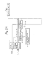
Images


Classifications
-
- G—PHYSICS
- G11—INFORMATION STORAGE
- G11C—STATIC STORES
- G11C29/00—Checking stores for correct operation ; Subsequent repair; Testing stores during standby or offline operation
-
- G—PHYSICS
- G11—INFORMATION STORAGE
- G11C—STATIC STORES
- G11C29/00—Checking stores for correct operation ; Subsequent repair; Testing stores during standby or offline operation
- G11C29/70—Masking faults in memories by using spares or by reconfiguring
- G11C29/78—Masking faults in memories by using spares or by reconfiguring using programmable devices
- G11C29/84—Masking faults in memories by using spares or by reconfiguring using programmable devices with improved access time or stability
- G11C29/842—Masking faults in memories by using spares or by reconfiguring using programmable devices with improved access time or stability by introducing a delay in a signal path
Definitions
- the present invention relates to a semiconductor memory device. Particularly, the present invention relates to a semiconductor memory device having a redundancy memory cell array.
- a conventional semiconductor memory device is provided with a row control circuit, a row address buffer, a row decoder and driver, a regular memory cell array, a sense amplifier, a column address buffer, a column decoder, and so on.
- a row address strobe signal RAS is input to the row control circuit from the outside, and the row control circuit supplies control signals to the row address buffer and the row decoder and driver at a predetermined timing, respectively.
- the control signal is supplied from the row control circuit to the row address buffer.
- the row address buffer then supplies row address bit signals to the row decoder and driver, and when the potential levels of the row address bit signals output from the row address buffer have been established, the control signal is supplied from the row control circuit to the row decoder and driver.
- the row decoder and driver then select a predetermined work line, and the potential thereof is raised in accordance with the potential levels of the input row address bit signals.
- data stored in a predetermined memory cell arranged at the intersection of the selected word line and a selected bit line provided in the regular memory cell array is read out through the selected bit line, sense amplifier, and data bus provided in the column decoder.
- predetermined data is written from the outside to the predetermined memory cell connected to the selected. word line through the data bus and the selected bit line.
- the column decoder selects a predetermined bit line in accordance with potential levels of the input column address bit signals supplied from the column address buffer.
- a type of semiconductor memory device having a redundancy memory cell array in addition to the regular memory array.
- a programming circuit for programming defective address bits corresponding to a defective memory cell existing in the regular memory cell array
- a comparison circuit for comparing each logic of the input address bits (for example, input row address bit signals) with each of the programmed defective address bits and for detecting whether or not each logic of the input row address bits coincides with each of the programmed address bits
- a switching circuit for supplying control signals to the row decoder and driver for the regular memory cell array or for the redundancy memory cell array, respectively, m accordance with the result of the above comparison.
- a control signal is supplied from the row control circuit to the comparison circuit.
- the comparison circuit compares each logic of the input row address bits with each logic of the defective address bits programmed in the programming circuit, and an output signal having a predetermined potential level is supplied from the comparison circuit to the switching circuit in accordance with the result of the comparison.
- a control signal is supplied from the row control circuit to the switching circuit, and the switching circuit carries out a switching operation in accordance with the logic of the output signal from the comparison circuit.
- the comparison circuit detects that at least one logic of the input row address bits does not coincide with the corresponding defective row address bit programmed in the programming circuit, the potential of the output signal from the comparison circuit becomes low level, for example, and when the potential level of the output signal from the comparison circuit has been set to low level, the above control signal from the row control circuit is supplied through the switching circuit to the row decoder and driver, to select a predetermined work line provided in the regular memory cell array in accordance with the potential levels of the input row address bit signals.
- data stored in a predetermined memory cell arranged at the intersection of the selected word line and the selected bit line provided in the regular memory cell array is read out, or predetermined data is written from the outside to the predetermined memory cell.
- the comparison circuit detects that each logic of the input row address bits coincides with each of the defective row address bits programmed in the programming circuit, the potential of the output signal from the comparison circuit becomes high level, for example, and when the potential level of the output signal from the comparison circuit has been set to high level, the above control signal from the row control circuit is supplied through the switching circuit to the redundancy row decoder and driver, to select a predetermined redundancy word line provided in the redundancy memory cell array in accordance with the input row address bit signals corresponding to the programmed defective address bits.
- the time required for selecting a predetermined word line provided in the regular memory cell array or the redundancy memory cell array is delayed by the time required for establishing the potential level of the output signal supplied from the comparison circuit to the switching circuit, compared with the time required for selecting a predetermined word line provided in the regular memory cell array in the memory device not having the redundancy memory cell array.
- the present invention has been made in view of the above-mentioned problem, and an embodiment of the present invention may increase the access speed for the predetermined memory cell corresponding to the selected address bits when defective address bits are not programmed in the programming circuit in a semiconductor memory device having a redundancy memory cell array.
- a semiconductor memory device comprising a regular memory cell array in which a plurality of word lines and bit lines are provided, and a plurality of memory cells are arranged at intersections of the word lines and bit lines; a redundancy memory cell array in which one or more word lines and bit lines are provided, and a plurality of memory cells are arranged at intersections of the word lines and bit lines; control means for generating a first control signal; means for programming defective address bits corresponding to defective memory cells existing in the regular memory cell array; means for comparing the logics of input address bits with the defective address bits; a first switching means for generating a second control signal when at least one logic of the input address bits does not coincide with the corresponding defective address bit and for supplying a third control signal to a predetermined word line or bit line belonging to the redundancy memory cell array without generating the second control signal when the logics of the input address bits coincide with the defective address bits; means for identifying whether or not any defective address bits are programmed in the programming means; and
- a predetermined memory cell corresponding to the input address bits may be directly selected without comparing the logics of the input address bits with the defective address bits, and thus, it is possible to increase the access speed for the predetermined memory cell corresponding to the input address bits when the defective address bits are not programmed in the programming means.
- Fig. 5 is a timing chart concerning the potential changes of several signals and a selected word line in the device shown in Fig. I.
- reference numeral I is a row control circuit to which a row address strobe signal RAS is input from the outside, and generated control signals ⁇ ADD and ⁇ WL each generated at a predetermined timing as described below.
- Reference numeral 2 is a row address buffer to which external row address bit signals A o to A n having TTL (Transistor-Transistor-Logic) potential levels are input, and at the timing when the potential level of the signal PAS becomes low, the control signal 0 ADD is supplied from the row control circuit I to the row address buffer 2. Accordingly, the row address buffer 2 outputs row address bit signals A o to A n and A o (an inverted bit signal of A o ) to A n (an inverted bit signal of An) each having a MOS potential level (i.e., the high level and the low level corresponding to the V cc level and V ss level, respectively), as shown in Fig. 5.
- TTL Transistor-Transistor-Logic
- Reference numeral 3 is a row decoder and driver to which the row address bit signals A o to An and A o to A n are supplied from the row address buffer 2, and at the timing "t o " shown in Fig. 5 at which potential levels of the above signals A o to An and A o to A n output from the row address buffer 2 have been established (in this connection, Fig. 5 shows that the potential levels of row address bit signals A; and A j are high, and therefore, the potential levels of the corresponding inverted row address bit signals A i and A j are low), the control signal ⁇ WL is supplied from the row control circuit I to the row decoder and driver 3. Accordingly, the row decoder and driver 3 selects a predetermined word line, for example, WL,, in accordance with the potential levels of the input row address bit signals A o to A n and A o to A n .
- a circuit portion 31 provided in the above row decoder and driver 3 is an example of a decoder and driver circuit for selecting the word line WL, when the potential levels of the input row address bit signals A o to An are all low (i.e., the potential levels of the input row address bit signals A o to A n are all high).
- the potential level of a control signal 0 changes in phase with that of the signal RAS , and when the potential level of the signal ⁇ is high, a precharging transistor Q 10 is turned ON, and the potential of a node p corresponding to the connecting point between the precharging transistor Q 10 and decoding transistors Q,, to Q 1n becomes high level (V cc level).
- At this time if at least one of the potential levels of the input row address bit signals A o to Anis high (i.e., at least one potential levels of the input row address bit signals A o to A n is low), at least one of the decoding transistors Q,, to Q 1n is turned ON, and thus the potential of the node p in the above circuit 31 becomes low. Accordingly, the potential of the corresponding word line WL, does not become high. As a result, the word line WL, is non-selected, and another predetermined word line is selected by the corresponding decoder and driver circuit in accordance with the potential levels of the input row address bit signals A o to A n and A o to A n .
- Reference numeral 41 is a regular memory cell array in which a plurality of word lines (WL,, and so on) and a plurality of bit lines (BL, to BL m ) are provided, and a plurality of memory cells (MC,, to MC 1m , and so on) are arranged at each intersection of the word lines and bit lines.
- Each of the memory cells (for example, MC,,) comprises a transfer gate transsistor Q 11 and a capacitor C,, for storing data.
- the potential of the selected word line WL is raised as above-mentioned. Accordingly, the data stored in the capacitor C, is supplied to a sense amplifier 51 through the transfer gate transistor Q, and the selected bit line BL,. This data is then sensed and amplified by the sense amplifier 51 and is output as output data D out through the selected bit line BL, and data bus provided in a column decoder 6.
- the data D in is supplied to the memory cell MC 11 through the above data bus, the selected bit line BL,, and the transfer gate transistor Q,, connected to the selected word line WL,.
- the column decoder 6 selects a predetermined bit line (for example, BL) in accordance with the potential levels of the input column address oit signals A' o to A' n and A' C to A' n
- Reference numeral 7 denotes a column address buffer to which external column address bit signals A' o to A' n are input and the column address buffer 7 suppes the column address bit signals A' o to A' n and A' o to
- Figure 2 shows an example of the construction of a previously proposed semiconductor memory device in which a reaundancy memory cell array 42 is provided in addition to the regular memory cell array 41.
- Figure 6 is a timing chart for the potential changes of several signals and a selected word line in the device shown in Fig. 2.
- the test for the regular memory cell array 41 is carried out before forwarding the device to the next process, in order to detect whether or not a defective memory cell exists in the regular memory cell array 41. Accordingly, if a defective memory cell is detected, the defective address bit signals corresponding to the defective memory cell (in this case, defective row address bits) are programmed (stored) in a programming circuit (for example, a read only memory) 8 for programming the defective address bits.
- a programming circuit for example, a read only memory
- a control signal ⁇ CM is supplied from the row control circuit I to a comparison circuit 9.
- the comparison circuit 9 compares each logic (in this case, each potential) of the row address bit signals (for example, A o to An) input thereto with each logic of the defective address bits programmed in the programming circuit (ROM) 8, and an output signal ⁇ CMP having a predetermined potential level is supplied from the comparison circuit 9 to a switching circuit 10 in accordance with the result of the comparison. As shown in Fig.
- the output signal ⁇ CMP is generated at the above timing "t a " by supplying the above control signal ⁇ CM from the row control circuit I to the comparison circuit 9. Further, when the potential level of the output signal ⁇ CPM has been established at the timing "t' o " shown in Fig. 6, the control signal ⁇ B is supplied from the row control circuit I to the switching circuit 10, and the switching circuit 10 carries out the switching operation in accordance with the logic (in this case, the potential level) of the output signal ⁇ CMP .
- the comparison circuit 9 detects that at least one logic of the input row address bits A o to An does not coincide with the corresponding defective row address bit programmed in the programming circuit 8, the potential of the output signal ⁇ CMP becomes low level, for example.
- the above control signal ⁇ B is supplied through the switching circuit 10 to the word decoder and driver 3, as the control signal ⁇ WL for a selected word line.
- the word decoder and driver 3 raises the potential WL (shown in Fig. 6) of the selected word line (for example, WL,) provided in the regular memory cell array 41, in accordance with the potential levels of the input row address bit signals A o to A n and A o to A n .
- data stored in a predetermined memory cell MC 11 for example, arranged at the intersection of the selected word line (for example, WL,) and the selected bit line (for example, BL,) is read out as the output data Pout, or the input data D in is written to the predetermined memory cell (for example, MC,,), as above-mentioned.
- the comparison circuit 9 detects that each logic of the input row address bits A o to An coincides with each of the defective row address bits programmed in the programming circuit 8, the potential of the output signal ⁇ CMP becomes high level, for example.
- the above control signal ⁇ B is supplied through the switching circuit 10 to a redundancy word line WL R provided in the redundancy memory cell array 42, as a control signal ⁇ WLR for the above redundancy word line.
- the potential WLR (shown in Fig. 6) of the redundancy word line WL R becomes high level. Accordingly, data stored in a predetermined redundancy memory cell MC R11 , for example, arranged at the intersection of the redundancy word line WL R and the selected bit line (for example, BL,) is read out as the output data D out, or the input data D in is written to the predetermined redundancy memory cell (for example, MC R11 ). At this time, the word line coresponding to the defective row address, for example, WL, , provided in the regular memory cell array 41 is in a non-selected state.
- the time required for selecting a predetermined word line provided in the regular memory cell array 41 or the redundancy memory cell array 42 is delayed compared with the above time in the memory device not having the redundancy memory cell array as shown in Fig. I, due to the switching operation of the switching circuit 10 based on the potential level of the output signal ⁇ CMP -supplied from the comparison circuit 9.
- the timing "f o " shown in Fig. 6 at which the potential WL of the selected word line or the potential WLR of the selected redundancy word line rises is delayed compared with the timing "t' o " shown in Fig. 5 at which the potential WL of the selected word line rises in the memory device shown in Fig. I.
- Figure 3 shows the overall construction of the semiconductor memory device according to one embodiment of the present invention.
- Figure 7A and Fig. 7B are timing charts concerning the potential changes of several signals and a selected word line in the device shown in Fig. 3.
- Fig. 7A corresponds to the time chart in the case wherein defective address bits are not programmed in the programming circuit (ROM) 8
- Fig. 7B corresponds to-the time chart in the case wherein the defective address bits are programmed in the programming circuit (ROM) 8.
- the comparison circuit 9 detects that at least one logic of the input row address bits A o to An does not coincide with corresponding defective row address bit programmed in the programming circuit 8, the potential of the output signal 0 CMP becomes low level, for example. Accordingly, at the above timing "t' o ", at which the potential level of the above signal ⁇ CMP has been set to a low level, the above control signal ⁇ B is supplied from the row control circuit I to the switching circuit 10, and thus, the switching circuit 10 supplies a control signal ⁇ WLB to a switching circuit 12 as described below.
- the comparison circuit 9 detects that each logic of the input row address bits A o to An coincides with each of the defective row address bits programmed in the programming circuit 8, the potential of the output signal ⁇ CMP becomes high level, for example. Accordingly, at the above timing "t' o ", at which the potential level of the above signal ⁇ CMP has been set to a high level, the above control signal ⁇ B is supplied through the switching circuit 10 to the redundancy word line WL R as the control signal ⁇ WLR . As a result, the potential WLR (shown in Fig. 7B) of the redundancy word line WL R becomes high level.
- data stored in the predetermined redundancy memory cell MC R11 is read out as the output data D out , or the input data D in is written to the predetermined redundancy memory cell (for example, MC R11 ).
- the word line corresponding to the defective row address, for example WL, provided in the regular memory cell array 41 is in a non-selected state.
- redundancy word line WL R is provided in the redundancy memory cell array 42, it is also possible to provide a plurality of redundancy word lines in the redundancy memory cell array and to select a predetermined redundancy word line in accordance with selected defective row address bits programmed in the programming circuit by using a redundancy row decoder and driver.
- the test is carried out before forwarding the device to the next process, in order to detect whether or not a defective memory cell exists in the regular memory cell array 41.
- the defective address bits for example, defective row address bits
- the programming circuit for example, ROM
- the control signal ⁇ WLR is supplied from the switching circuit 10 to the redundancy word line WL R , and the access for a predetermined redundancy memory cell is carried out instead of the access for a corresponding memory cell arranged in the regular memory cell array.
- another programming circuit II for example, a ROM
- a ROM for programming data identifying whether or not any defective address bits are programmed in the programming circuit 8 (i.e., whether or not the redundancy memory cell array is used) is provided in addition to the above programming circuit 8.
- the potential of an output signal RDT supplied from the programming circuit II is set to high level by programming a high level data "I" in the programming circuit II, and when defective address bits are not programmed in the programming circuit 8, (i.e., when the redundancy memory cell array is not used), the potential of the output signal RDT is set to low level by programming a low level data "0" in the programming circuit II.
- the above predetermined one bit logic data identifying whether or not the defective address bits are programmed in the programming circuit 8 is previously written to the programming circuit (ROM) II before the operation of the memory device in accordance with the result of the above-mentioned test carried out before the forwarding (shipping) of the device.
- the output signal RDT having a predetermined potential level is also supplied from the above programming circuit II to the switching circuit 12 during the operation of the memory device.
- the signal path through which a control signal ⁇ WLA output from the row control circuit I is supplied to the word decoder and driver 3 as the control signal ⁇ WL is formed by the switching circuit 12.
- the control signal ⁇ WLA is supplied from the row control circuit I to the switching circuit 12 at the timing "to" shown in Fig. 7A which corresponds to the timing "to” shown in Fig. 5, and then the control signal ⁇ WL for selecting a predetermined word line provided in the regular memory cell array 41 is supplied from the switching circuit 12 to the word decoder and driver 3, as shown in Fig. 7A.
- the signal path through which the control signal ⁇ WL - s output from the switching circuit 10 is supplied to the word decoder and driver 3 as the control signal ⁇ w L is formed by the switching circuit 12, and then the control signal ⁇ wL is supplied from the switching circuit 12 to the word decoder and driver 3, as shown in Fig. 7B.
- the setting of one of the above-mentioned signal paths is completed in the switching circuit 12 before the operation word line selection of the memory device in accordance with the potential level of the output signal RDT.
- the access timing for a predetermined memory cell provided in the regular memory cell array 41 in the memory device shown in Fig. 3 is substantially the same as that in the memory device shown in Fig. 2.
- the access timing for a predetermined memory cell provided in the regular memory cell array 41 in the memory device shown in Fig. 3 is substantially the same as that in the memory device shown in Fig. I, and thus, it is possible to increase the access speed in the latter case.
- Figure 4 is a circuit diagram showing an example of the switching circuit 12.
- a transistor Q4 is turned ON through a turned-ON transistor Q2 , and the control signal ⁇ WLB is supplied from the switching circuit 10 to the word decoder and driver 3 as the control signal 0 WL .
- the defective row address bits are used as defective address data, it is also possible to use defective column address bits as such defective address data.
Landscapes
- For Increasing The Reliability Of Semiconductor Memories (AREA)
- Dram (AREA)
- Techniques For Improving Reliability Of Storages (AREA)
- Read Only Memory (AREA)
Applications Claiming Priority (2)
| Application Number | Priority Date | Filing Date | Title |
|---|---|---|---|
| JP61060929A JPS62222500A (ja) | 1986-03-20 | 1986-03-20 | 半導体記憶装置 |
| JP60929/86 | 1986-03-20 |
Publications (3)
| Publication Number | Publication Date |
|---|---|
| EP0242981A2 true EP0242981A2 (de) | 1987-10-28 |
| EP0242981A3 EP0242981A3 (en) | 1989-12-13 |
| EP0242981B1 EP0242981B1 (de) | 1992-01-02 |
Family
ID=13156562
Family Applications (1)
| Application Number | Title | Priority Date | Filing Date |
|---|---|---|---|
| EP87302312A Expired - Lifetime EP0242981B1 (de) | 1986-03-20 | 1987-03-18 | Halbleiter-Speicheranordnung mit Redundanzschaltungsteil |
Country Status (5)
| Country | Link |
|---|---|
| US (1) | US4803656A (de) |
| EP (1) | EP0242981B1 (de) |
| JP (1) | JPS62222500A (de) |
| KR (1) | KR900008637B1 (de) |
| DE (1) | DE3775603D1 (de) |
Cited By (5)
| Publication number | Priority date | Publication date | Assignee | Title |
|---|---|---|---|---|
| EP0337384A3 (de) * | 1988-04-12 | 1991-07-17 | Nec Corporation | In ein Halbleiterspeichergerät eingebaute Redundanzschaltung |
| EP0377827A3 (de) * | 1989-01-13 | 1991-07-31 | International Business Machines Corporation | Verstärkungstaktsignalgenerator |
| EP0448958A3 (en) * | 1990-02-23 | 1992-07-15 | Kabushiki Kaisha Toshiba | Semiconductor integrated circuit having non-volatile memory cells for controlling a predetermined function |
| GB2256070A (en) * | 1991-05-24 | 1992-11-25 | Samsung Electronics Co Ltd | Semiconductor memory device with redundancy |
| WO1997043713A1 (en) * | 1996-05-10 | 1997-11-20 | Memory Corporation Plc | Substitute memory timing circuit |
Families Citing this family (21)
| Publication number | Priority date | Publication date | Assignee | Title |
|---|---|---|---|---|
| US5022006A (en) * | 1988-04-01 | 1991-06-04 | International Business Machines Corporation | Semiconductor memory having bit lines with isolation circuits connected between redundant and normal memory cells |
| EP0389203A3 (de) * | 1989-03-20 | 1993-05-26 | Fujitsu Limited | Halbleiterspeichergerät beinhaltend Information, die die Anwesenheit mangelhafter Speicherzellen anzeigt |
| JP2547633B2 (ja) * | 1989-05-09 | 1996-10-23 | 三菱電機株式会社 | 半導体記憶装置 |
| US5184327A (en) * | 1989-06-14 | 1993-02-02 | Mitsubishi Denki Kabushiki Kaisha | Semiconductor memory device having on-chip test circuit and method for testing the same |
| JPH0748320B2 (ja) * | 1989-07-24 | 1995-05-24 | セイコー電子工業株式会社 | 半導体不揮発性メモリ |
| JPH03252998A (ja) * | 1990-02-28 | 1991-11-12 | Sharp Corp | 半導体記憶装置 |
| EP0527866B1 (de) * | 1990-05-10 | 1994-04-13 | Siemens Aktiengesellschaft | Integrierter halbleiterspeicher mit paralleltestmöglichkeit und redundanzverfahren |
| US5276834A (en) * | 1990-12-04 | 1994-01-04 | Micron Technology, Inc. | Spare memory arrangement |
| JPH0620494A (ja) * | 1992-06-30 | 1994-01-28 | Hitachi Ltd | 半導体記憶装置 |
| JPH06119796A (ja) * | 1992-10-06 | 1994-04-28 | Texas Instr Japan Ltd | 欠陥メモリセル救済用デコーダ |
| JPH06242925A (ja) * | 1993-02-15 | 1994-09-02 | Mitsubishi Electric Corp | ソート処理装置 |
| US5526503A (en) * | 1993-10-06 | 1996-06-11 | Ast Research, Inc. | Virtual addressing buffer circuit |
| US5495447A (en) * | 1993-10-08 | 1996-02-27 | Digital Equipment Corporation | Method and apparatus using mapped redundancy to perform multiple large block memory array repair |
| US5461586A (en) * | 1994-01-31 | 1995-10-24 | Texas Instruments Incorporated | Self-timed redundancy circuit |
| GB9417269D0 (en) * | 1994-08-26 | 1994-10-19 | Inmos Ltd | Memory and test method therefor |
| JP3226425B2 (ja) * | 1994-09-09 | 2001-11-05 | 富士通株式会社 | 半導体記憶装置 |
| JP3425811B2 (ja) * | 1994-09-28 | 2003-07-14 | Necエレクトロニクス株式会社 | 半導体メモリ |
| US5640353A (en) * | 1995-12-27 | 1997-06-17 | Act Corporation | External compensation apparatus and method for fail bit dynamic random access memory |
| EP0811917B1 (de) * | 1996-06-06 | 2002-01-02 | STMicroelectronics S.r.l. | Schaltung um redundante Daten einer Redundanzschaltung innerhalb einer Speicheranordnung durch zeitgeteilte Annäherung zu übertragen |
| JP4062247B2 (ja) * | 2003-12-11 | 2008-03-19 | ソニー株式会社 | 半導体記憶装置 |
| KR100541819B1 (ko) * | 2003-12-30 | 2006-01-10 | 삼성전자주식회사 | 스타트 프로그램 전압을 차등적으로 사용하는 불휘발성반도체 메모리 장치 및 그에 따른 프로그램 방법 |
Family Cites Families (11)
| Publication number | Priority date | Publication date | Assignee | Title |
|---|---|---|---|---|
| US4228528B2 (en) * | 1979-02-09 | 1992-10-06 | Memory with redundant rows and columns | |
| DE3071955D1 (en) * | 1979-06-15 | 1987-05-27 | Fujitsu Ltd | Semiconductor memory device |
| US4441170A (en) * | 1980-09-30 | 1984-04-03 | Intel Corporation | Memory redundancy apparatus for single chip memories |
| JPS6051199B2 (ja) * | 1980-11-13 | 1985-11-12 | 富士通株式会社 | 半導体装置 |
| US4376300A (en) * | 1981-01-02 | 1983-03-08 | Intel Corporation | Memory system employing mostly good memories |
| US4422161A (en) * | 1981-10-08 | 1983-12-20 | Rca Corporation | Memory array with redundant elements |
| US4480199A (en) * | 1982-03-19 | 1984-10-30 | Fairchild Camera & Instrument Corp. | Identification of repaired integrated circuits |
| JPS595497A (ja) * | 1982-07-02 | 1984-01-12 | Hitachi Ltd | 半導体rom |
| JPS59203299A (ja) * | 1983-05-06 | 1984-11-17 | Nec Corp | 冗長ビット付メモリ |
| JPS6089899A (ja) * | 1983-10-24 | 1985-05-20 | Nec Corp | メモリ回路 |
| JPS60114025A (ja) * | 1983-11-25 | 1985-06-20 | Nec Corp | パルス回路 |
-
1986
- 1986-03-20 JP JP61060929A patent/JPS62222500A/ja active Granted
-
1987
- 1987-03-18 EP EP87302312A patent/EP0242981B1/de not_active Expired - Lifetime
- 1987-03-18 DE DE8787302312T patent/DE3775603D1/de not_active Expired - Lifetime
- 1987-03-20 KR KR1019870002571A patent/KR900008637B1/ko not_active Expired
- 1987-03-20 US US07/028,463 patent/US4803656A/en not_active Expired - Fee Related
Cited By (6)
| Publication number | Priority date | Publication date | Assignee | Title |
|---|---|---|---|---|
| EP0337384A3 (de) * | 1988-04-12 | 1991-07-17 | Nec Corporation | In ein Halbleiterspeichergerät eingebaute Redundanzschaltung |
| EP0377827A3 (de) * | 1989-01-13 | 1991-07-31 | International Business Machines Corporation | Verstärkungstaktsignalgenerator |
| EP0448958A3 (en) * | 1990-02-23 | 1992-07-15 | Kabushiki Kaisha Toshiba | Semiconductor integrated circuit having non-volatile memory cells for controlling a predetermined function |
| GB2256070A (en) * | 1991-05-24 | 1992-11-25 | Samsung Electronics Co Ltd | Semiconductor memory device with redundancy |
| FR2676844A1 (fr) * | 1991-05-24 | 1992-11-27 | Samsung Electronics Co Ltd | Dispositif de memoire a semiconducteurs avec redondance. |
| WO1997043713A1 (en) * | 1996-05-10 | 1997-11-20 | Memory Corporation Plc | Substitute memory timing circuit |
Also Published As
| Publication number | Publication date |
|---|---|
| KR900008637B1 (ko) | 1990-11-26 |
| US4803656A (en) | 1989-02-07 |
| EP0242981A3 (en) | 1989-12-13 |
| JPH0526280B2 (de) | 1993-04-15 |
| KR870009383A (ko) | 1987-10-26 |
| JPS62222500A (ja) | 1987-09-30 |
| EP0242981B1 (de) | 1992-01-02 |
| DE3775603D1 (de) | 1992-02-13 |
Similar Documents
| Publication | Publication Date | Title |
|---|---|---|
| US4803656A (en) | Semiconductor memory device having redundancy circuit portion | |
| KR960002014B1 (ko) | 결점을 수리하는 용장메모리셀 어레이를 포함하는 반도체 기억장치 | |
| US4365319A (en) | Semiconductor memory device | |
| US4667330A (en) | Semiconductor memory device | |
| KR100386442B1 (ko) | 메모리디바이스회로 및 멀티뱅크메모리어레이의 멀티뱅크컬럼의동시어드레스방법 | |
| US4766573A (en) | Semiconductor memory device with error correcting circuit | |
| US5155705A (en) | Semiconductor memory device having flash write function | |
| EP0031386B1 (de) | Halbleiter-speichervorrichtung | |
| US6324105B1 (en) | Redundant row topology circuit, and memory device and test system using same | |
| US4473895A (en) | Semiconductor memory device | |
| US6269035B1 (en) | Circuit and method for a multiplexed redundancy scheme in a memory device | |
| US5122987A (en) | Semiconductor memory device with individually addressable space cells capable of driving a data bus | |
| US5379259A (en) | Semiconductor memory device | |
| JP2773271B2 (ja) | 半導体記憶装置 | |
| JP2000163988A (ja) | 半導体記憶装置 | |
| EP0102618A2 (de) | Speicherschaltung mit Mitteln zum Nachweis der Speisespannung | |
| US5566128A (en) | Semiconductor memory device | |
| KR940005697B1 (ko) | 용장 메모리 셀을 갖는 반도체 메모리 장치 | |
| KR900006162B1 (ko) | 결함 메모리 어드레스용 읽기회로를 구비한 용장성 구조를 갖는 반도체 메모리 | |
| US5805515A (en) | Semiconductor memory device for high speed operation | |
| US6851017B2 (en) | Semiconductor memory | |
| US6330198B1 (en) | Semiconductor storage device | |
| JPH05109279A (ja) | マルチポートメモリ | |
| JP2953119B2 (ja) | 半導体集積回路 | |
| JP3898390B2 (ja) | 半導体記憶装置 |
Legal Events
| Date | Code | Title | Description |
|---|---|---|---|
| PUAI | Public reference made under article 153(3) epc to a published international application that has entered the european phase |
Free format text: ORIGINAL CODE: 0009012 |
|
| AK | Designated contracting states |
Kind code of ref document: A2 Designated state(s): DE FR GB |
|
| PUAL | Search report despatched |
Free format text: ORIGINAL CODE: 0009013 |
|
| AK | Designated contracting states |
Kind code of ref document: A3 Designated state(s): DE FR GB |
|
| 17P | Request for examination filed |
Effective date: 19891219 |
|
| 17Q | First examination report despatched |
Effective date: 19910409 |
|
| GRAA | (expected) grant |
Free format text: ORIGINAL CODE: 0009210 |
|
| AK | Designated contracting states |
Kind code of ref document: B1 Designated state(s): DE FR GB |
|
| REF | Corresponds to: |
Ref document number: 3775603 Country of ref document: DE Date of ref document: 19920213 |
|
| ET | Fr: translation filed | ||
| PLBE | No opposition filed within time limit |
Free format text: ORIGINAL CODE: 0009261 |
|
| 26N | No opposition filed | ||
| PGFP | Annual fee paid to national office [announced via postgrant information from national office to epo] |
Ref country code: GB Payment date: 19930105 Year of fee payment: 7 |
|
| PGFP | Annual fee paid to national office [announced via postgrant information from national office to epo] |
Ref country code: FR Payment date: 19930330 Year of fee payment: 7 |
|
| PGFP | Annual fee paid to national office [announced via postgrant information from national office to epo] |
Ref country code: DE Payment date: 19930521 Year of fee payment: 7 |
|
| PG25 | Lapsed in a contracting state [announced via postgrant information from national office to epo] |
Ref country code: GB Effective date: 19940318 |
|
| GBPC | Gb: european patent ceased through non-payment of renewal fee |
Effective date: 19940318 |
|
| PG25 | Lapsed in a contracting state [announced via postgrant information from national office to epo] |
Ref country code: FR Effective date: 19941130 |
|
| PG25 | Lapsed in a contracting state [announced via postgrant information from national office to epo] |
Ref country code: DE Effective date: 19941201 |
|
| REG | Reference to a national code |
Ref country code: FR Ref legal event code: ST |