EP0102618A2 - Speicherschaltung mit Mitteln zum Nachweis der Speisespannung - Google Patents
Speicherschaltung mit Mitteln zum Nachweis der Speisespannung Download PDFInfo
- Publication number
- EP0102618A2 EP0102618A2 EP83108582A EP83108582A EP0102618A2 EP 0102618 A2 EP0102618 A2 EP 0102618A2 EP 83108582 A EP83108582 A EP 83108582A EP 83108582 A EP83108582 A EP 83108582A EP 0102618 A2 EP0102618 A2 EP 0102618A2
- Authority
- EP
- European Patent Office
- Prior art keywords
- circuit
- power voltage
- value
- memory
- terminal
- Prior art date
- Legal status (The legal status is an assumption and is not a legal conclusion. Google has not performed a legal analysis and makes no representation as to the accuracy of the status listed.)
- Granted
Links
Images

Classifications
-
- H—ELECTRICITY
- H03—ELECTRONIC CIRCUITRY
- H03K—PULSE TECHNIQUE
- H03K17/00—Electronic switching or gating, i.e. not by contact-making and –breaking
- H03K17/22—Modifications for ensuring a predetermined initial state when the supply voltage has been applied
- H03K17/223—Modifications for ensuring a predetermined initial state when the supply voltage has been applied in field-effect transistor switches
-
- G—PHYSICS
- G01—MEASURING; TESTING
- G01R—MEASURING ELECTRIC VARIABLES; MEASURING MAGNETIC VARIABLES
- G01R19/00—Arrangements for measuring currents or voltages or for indicating presence or sign thereof
- G01R19/165—Indicating that current or voltage is either above or below a predetermined value or within or outside a predetermined range of values
- G01R19/16533—Indicating that current or voltage is either above or below a predetermined value or within or outside a predetermined range of values characterised by the application
- G01R19/16557—Logic probes, i.e. circuits indicating logic state (high, low, O)
-
- G—PHYSICS
- G05—CONTROLLING; REGULATING
- G05F—SYSTEMS FOR REGULATING ELECTRIC OR MAGNETIC VARIABLES
- G05F1/00—Automatic systems in which deviations of an electric quantity from one or more predetermined values are detected at the output of the system and fed back to a device within the system to restore the detected quantity to its predetermined value or values, i.e. retroactive systems
- G05F1/10—Regulating voltage or current
- G05F1/46—Regulating voltage or current wherein the variable actually regulated by the final control device is DC
- G05F1/56—Regulating voltage or current wherein the variable actually regulated by the final control device is DC using semiconductor devices in series with the load as final control devices
- G05F1/565—Regulating voltage or current wherein the variable actually regulated by the final control device is DC using semiconductor devices in series with the load as final control devices sensing a condition of the system or its load in addition to means responsive to deviations in the output of the system, e.g. current, voltage, power factor
- G05F1/569—Regulating voltage or current wherein the variable actually regulated by the final control device is DC using semiconductor devices in series with the load as final control devices sensing a condition of the system or its load in addition to means responsive to deviations in the output of the system, e.g. current, voltage, power factor for protection
- G05F1/571—Regulating voltage or current wherein the variable actually regulated by the final control device is DC using semiconductor devices in series with the load as final control devices sensing a condition of the system or its load in addition to means responsive to deviations in the output of the system, e.g. current, voltage, power factor for protection with overvoltage detector
-
- G—PHYSICS
- G06—COMPUTING OR CALCULATING; COUNTING
- G06F—ELECTRIC DIGITAL DATA PROCESSING
- G06F1/00—Details not covered by groups G06F3/00 - G06F13/00 and G06F21/00
- G06F1/26—Power supply means, e.g. regulation thereof
- G06F1/28—Supervision thereof, e.g. detecting power-supply failure by out of limits supervision
-
- G—PHYSICS
- G11—INFORMATION STORAGE
- G11C—STATIC STORES
- G11C5/00—Details of stores covered by group G11C11/00
- G11C5/14—Power supply arrangements, e.g. power down, chip selection or deselection, layout of wirings or power grids, or multiple supply levels
- G11C5/143—Detection of memory cassette insertion or removal; Continuity checks of supply or ground lines; Detection of supply variations, interruptions or levels ; Switching between alternative supplies
-
- G—PHYSICS
- G11—INFORMATION STORAGE
- G11C—STATIC STORES
- G11C8/00—Arrangements for selecting an address in a digital store
- G11C8/18—Address timing or clocking circuits; Address control signal generation or management, e.g. for row address strobe [RAS] or column address strobe [CAS] signals
Definitions
- the present invention relates to a static type memory circuit having a stand-by mode, or "Data Retention Mode", for allowing,stored information to be maintained by a back-up voltage of a smaller voltage value than a normal operation power voltage, and more particularly, to a memory circuit of the mentioned type having means for detecting reduction in a power supply voltage.
- a static type memory can operate at a high speed, but it requires a relatively large amount of power consumption.
- a value of the power supply voltage applied to the memory is reduced to a value which is enough to maintain information storage in memory cells but is not enough to perform write and read operationsto and from the memory cells, introducing "Data Retention Mode" to the memory.
- the Data Retention Mode is initiated by turning a chip selection signal applied to the memory chip to an inactive level for disenabling peripheral circuits of the memory cell array such as decoder circuits and a read/ write circuit, and by reducing the power voltage.
- the memory is provided with a voltage value detection circuit for detecting a drop in the power supply voltage for the Auto Data Retention Mode, and with a control circuit responsive to the chip selection signal and to the output of the voltage value detection circuit.
- the voltage value detection circuit in the prior art memory comprises a voltage divider circuit composed of resistors serially connected between the power voltage and a reference voltage for dividing the power voltage and of an inverter circuit receiving the output of the voltage divider circuit and logically distinguishing the value of the power voltage between the normal operation mode and Data Retention Mode.
- the output of the inverter of the voltage value detection circuit is then applied to one input terminal of a NOR gate which receives the chip selection signal at the other input terminal.
- the NOR gate produces an internal chip selection signal for directly controlling the peripheral circuits.
- a current always flows through the serially connected resistors both in the normal operation mode and in the Data Retention Mode, and therefore a considerable amount of power is inevitably consumed. This problem is more serious in the Data Retention Mode, because a battery is generally used as a back-up voltage source and its capacity is limited.
- a memory circuit comprises a voltage value detection circuit which includes a series connection of a chip selection signal detecting field effect transistor and a voltage value detecting field effect transistor.
- the gate of the former transistor receives a chip selection signal, and the latter transistor is adapted to be conducting when the potential at a power voltage terminal is in a first value and non-conducting when the potential at the power voltage terminal is in a second value smaller in absolute value than the first value, the second value being not enough to support the read/write operation of the memory circuit but enough to support information storage.
- This series connection is coupled via a load means between the power voltage terminal, and an output signal of the voltage value detection circuit is derived from the junction of the two transistors and the load means or from the junction between the two transistors.
- the voltage value detecting transistor is made non-conducting when the potential at the power voltage terminal is in the second value which brings the memory circuit into the Data Retention Mode, and hence no DC current flows the series connection in the voltage value detection circuit, resulting in a low power consumption.
- the voltage value detection circuit can be fabricated by a small number of circuit elements, e.g. one load element and two transistors, and hence the integration density of the memory circuit can be enhanced.
- a memory circuit compnsirga plurality of memory cells, a selection circuit for selecting at least one of the memory cells based on address information, a read circuit for operatively reading data from the memory cell or cells designated by the selection circuit, a write circuit for operatively writing data to the memory cell or cells designated by the selection circuit and an operation control circuit for controlling at least the read circuit and the write circuit in response both to a value of the power voltage variable between a first value and a second value smaller than the first value and to a chip selection signal having a first and second levels, the first value allowing the memory to normally operate, the second value inhibiting the memory from normally operating but allowing the memory to maintain stored data.
- the operation control circuit enabling and disenabling the write circuit and the read circuit in response to the first level and to the second level of the chip selection signal, respectively when the value of the power voltage is at the first value while the operation control circuit disenabling the.write circuit and the read circuit when the value of the power voltage is at the second value irrespectively of the chip selection signal, the operation control circuit including a load element coupled between a first terminal receiving one of the power voltage and a reference voltage and a second terminal, and a series circuit of a first field effect transistor receiving the chip selection signal at its gate and a second field effect transistor adapted to be conducting only when the power voltage is at the first value between the second terminal and a third terminal receiving the other of the power voltage and the reference voltage in which the controls of the write circuit and the read circuit are conducted in response to a potential at the second terminal.
- the potential at the second terminal can be controlled by the first transistor in response to the chip selection signal. While when the power voltage is at the second value and memory is to be in Data Retention Mode, the second transistor is non-conducting so that the - potential at the second terminal is determined through the load element independently on the chip selection signal so that the memory is automatically set at Data Retention Mode in which stored states of the memory cells are maintained but any access to the memory cells is inhibited. In this instance, no DC current flows the series circuit of the first and second transistors in the operation control circuit at least during Data Retention Mode. Accordingly, the power consumption in the operation control circuit is remarkably reduced. Furthermore, the operation control circuit can be fabricated by a small number of circuit elements so that the integration density of the memory can be enhanced.
- a memory cell array 22 includes a plurality of memory cells MC which are arranged in a matrix of word lines WL in rows and digit lines DL in columns.
- a plurality of row address input A O - An are applied to a row decoding circuit 24 through address inverter buffers 16.
- a column selection circuit 14 selectively connects one of the digit lines DL to a write data line WB and/or a read data line RB under control of a column decoder 15 to which column address inputs A n+1 Am are applied through column address inverter buffers 17.
- a mode control circuit 10 generates an internal control signal CS' in response to a chip selection signal CS from the outside and a value of a power voltage V cc* .
- the signal CS' is applied to an inverting input of a AND gate 21 receiving a write control signal WE at its another input, and to an inverting input of an AND gate receiving the write control signal WE at its another inverting input.
- the output of the gate 20 is used to operatively enable a data input buffer 18 for supplying data to be written in a write operation.
- the buffer 18 includes a series circuit of a P-channel transistor Q 22 and N-channel transistors Q 23 and Q24, and it is enabled when the transistor Q 24 is conducting.
- the output of the AND gate 21 is used to operatively enable an output buffer 19 receiving a read-out signal via the read data line RB.
- the buffer 19 includes a P-channel transistor Q 25 and N-channel transistors Q 26 and Q 27 , and it is enabled when the transistor Q 27 is conducting.
- the mode control circuit 10 includes a voltage value detection circuit 11, an inverter 12 and a NOR gate 13 receiving the chip selection signal CS and an output of the inverter 12.
- the voltage value detection circuit 10 includes a voltage divider composed of resistors R I and R 2 connected the power voltage V cc and a ground potential and a series circuit of a P-channel field effect transistor Q 1 and a resistor R 3 . With reference to Fig. 2, the operation of the memory will be described. When the value of the power voltage V cc is in a normal operation range, e.g.
- a voltage drop across the resistor R 1 i.e. a voltage difference between the voltage V and a voltage at a node N 1 is larger than a threshold voltage of the transistor Q 1 in absolute value so that a voltage at a node N 2 is larger than a logic threshold of the inverter in absolute value.
- the output of the inverter 12 necessarily takes logic "0" in the normal operation mode and hence the state of the signal CS is determined by the chip selection signal. For example, if the chip selection signal CS is at the logic "I”, then the signal CS' is at the logic "0" so that the memory is in active state. On the contrary, if the chip selection signal CS is at the logic "0" level, the signal CS' becomes the logic "1" so that the memory takes a stand-by state. In stand-by state, the input buffer 18 and the buffer 19 are inhibited so as not to affect the stored states of the memory cells.
- the memory of Fig. 1 can be automatically shift to Data Retention Mode by simply reducing the value of the power voltage V .
- a back-up voltage e.g. 3 V
- the voltage drop across the resistor R 1 becomes smaller than the threshold voltage of the transistor Q1
- the transistor Q 1 becomes non-conducting. Therefore, the potential at the node N 2 becomes the ground level i.e. logic "0".
- the signal CS' becomes the logic "1" irrespectively of the state of the chip selection signal CS so that the memory becomes the stand-by state, i.e. Data Retention Mode.
- the memory of Fig. 1 can be automatically shift to Data Retention Mode by simply reducing the value of the power voltage V .
- the memory of Fig. 1 can be automatically shift to Data Retention Mode by simply reducing the value of the power voltage V .
- the mode control circuit 10 is composed of a relatively large number of circuit elements and it is not desirable to fabricate the memory with high-density.
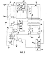
- the memory circuit of Fig. 3 is fabricated on a semiconductor chip.
- Fig. 3 the portions corresponding to those in Fig. 1 are designated by the same reference numbers used in Fig. 1.
- a mode control circuit 10' is employed in place of the mode control circuit 10 in Fig. 1.
- the mode control circuit 10' according to the invention includes a load resistor R 4 connected between the power voltage V cc and a node N 2 ', and a series circuit of an N-channel field effect transistor Q 20 receiving the chip select signal CS from the outside at a gate thereof and an N-channel field effect transistor Q 21 having a gate coupled to the power voltage V cc coupled between the node N 2 ' and the ground potential.
- each of decoding unit DU for driving the corresponding one of the word lines W L is composed of a P-channel field effect transistor Q 11 and an N-channel field effect transistor coupled between the power voltage V cc and the ground potential and both receiving the signal CS' at their gates, and a plurality of N-channel field effect transistors Q13 ....
- a threshold voltage of the N-channel transistor Q21 is selected to a value which is lower than the value of the power voltage V cc in the normal operation mode and larger than the value of the power voltage V CC in Data Retention Mode.
- the transistor Q 21 is conducting. Therefore, when the chip selection signal CS is at the logic "1", the transistor Q 20 is conducting so that the a potential at the rode N 2 ', i.e. the signal CS' is at the logic "0" through the conducting transistors Q 20 and Q 21 and the memory operates in the active mode.
- the OR gates 31 directly transfer the row address input A 0 - An to the row address inverter buffers 16 and the OR gates 33 directly transfer the column address inputs A n+1 -A n to the column address inverter buffers 17.
- the respective decoding units DU are enabled.
- the write control signal WE is at the logic "1"
- the output of the AND gate 21 is at the logic "1” while the output of the AND gate 20 is at the logic "0”. Therefore, the read buffer 19 is enabled while the write buffer 18 is disenabled.
- the write control signal WE is at the logic "0” and hence the write buffer 18 is enabled with the read buffer 19 disenabled.
- the transistor Q20 becomes non-conducting to make the signal CS' the logic "1" so that the memory takes a stand-by state, in which the outputs of the OR gates 31 and 33 are all logic “1” irrespectively of the address inputs so that changes of the states of the address inverter buffers 16 and 17 are inhibited. Accordingly, the power consumption generated in the address inverter buffers 16 and 17 can be avoided. Simultaneously, the load transistor Q 11 in the decoding unit DU is turned off and both the read buffer 19 and the write buffer 18 are disenabled.
- the transistor Q21 becomes non-conducting. Accordingly, the signal CS' becomes the logic "1" irrespectively of the chip selection signal CS so that the memory is shifted to the stand-by mode and the peripheral circuits such as the address inverter buffers 16 and 17, the read buffer 19 and the write buffer 18 are disenabled. According to the present invention, there is no DC current path in the mode control circuit 10' at least during Data Retention Mode so that the memory operable with a low power consumption is obtained. Furthermore, the control circuit 10' can be fabricated with a small number of circuit elements.
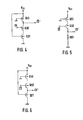
- a mode control circuit shown in Fig. 4 is obtained by replacing the resistor R 4 of Fig. 3 with a P-channel field effect transistor Q 41 having a gate connected to the ground potential.
- the operation of this mode control circuit is substantially the same as that of the circuit 10' of Fig. 3.
- a mode control circuit of Fig. 5 is the case where the logic system with respect to the chip selection signal C S and the internal control signal CS t of Fig. 3 is inverted. Namely, a series circuit of P-channel field effect transistors Q 51 and Q 52 is connected between a node N 2 " and the power voltage V cc and a resistor R 51 is connected between the node N 2 " and the ground potential.
- the transistor Q 51 when the value of the power voltage V cc changes from the value in the normal operation mode to that in Data Retention mode, the transistor Q 51 becomes non-conducting so that the signal C S' becomes the inactive level i.e. logic "0", because the threshold voltage of the transistor Q 51 is set slightly larger than the voltage value of the power voltage in Data Retention Mode.
- a mode control circuit of Fig. 6 is obtained by replacing the resistor R 51 of Fig. 5 with an N-channel transistor Q 61 having a gate connected to the power voltage. An operation of this circuit is similar to that of F ig. 5.
Landscapes
- Engineering & Computer Science (AREA)
- Physics & Mathematics (AREA)
- General Physics & Mathematics (AREA)
- Theoretical Computer Science (AREA)
- General Engineering & Computer Science (AREA)
- Microelectronics & Electronic Packaging (AREA)
- Electromagnetism (AREA)
- Radar, Positioning & Navigation (AREA)
- Automation & Control Theory (AREA)
- Power Engineering (AREA)
- Static Random-Access Memory (AREA)
Applications Claiming Priority (2)
| Application Number | Priority Date | Filing Date | Title |
|---|---|---|---|
| JP150844/82 | 1982-08-31 | ||
| JP57150844A JPS5940393A (ja) | 1982-08-31 | 1982-08-31 | メモリ回路 |
Publications (3)
| Publication Number | Publication Date |
|---|---|
| EP0102618A2 true EP0102618A2 (de) | 1984-03-14 |
| EP0102618A3 EP0102618A3 (en) | 1987-07-29 |
| EP0102618B1 EP0102618B1 (de) | 1990-06-06 |
Family
ID=15505609
Family Applications (1)
| Application Number | Title | Priority Date | Filing Date |
|---|---|---|---|
| EP83108582A Expired EP0102618B1 (de) | 1982-08-31 | 1983-08-31 | Speicherschaltung mit Mitteln zum Nachweis der Speisespannung |
Country Status (4)
| Country | Link |
|---|---|
| US (1) | US4631707A (de) |
| EP (1) | EP0102618B1 (de) |
| JP (1) | JPS5940393A (de) |
| DE (1) | DE3381632D1 (de) |
Cited By (5)
| Publication number | Priority date | Publication date | Assignee | Title |
|---|---|---|---|---|
| DE3521480A1 (de) * | 1984-06-15 | 1985-12-19 | Hitachi, Ltd., Tokio/Tokyo | Speichervorrichtung |
| FR2613491A1 (fr) * | 1987-04-03 | 1988-10-07 | Thomson Csf | Dispositif de detection du niveau haut d'une tension en technologie mos |
| EP0303257A1 (de) * | 1987-08-13 | 1989-02-15 | Kabushiki Kaisha Toshiba | Schaltung zur Erzeugung eines Rücksetzsignals |
| DE4003824A1 (de) * | 1989-05-19 | 1990-11-22 | Mitsubishi Electric Corp | Dynamischer speicher mit wahlfreiem zugriff mit einer mehrzahl von nennspannungen als betriebsversorgungsspannung und verfahren fuer dessen betreibung |
| EP0478253A3 (en) * | 1990-09-26 | 1993-06-16 | Sgs-Thomson Microelectronics, Inc. (A Delaware Corp.) | A semiconductor memory with power-on reset controlled latched row line repeaters |
Families Citing this family (13)
| Publication number | Priority date | Publication date | Assignee | Title |
|---|---|---|---|---|
| GB8611794D0 (en) * | 1986-05-14 | 1986-06-25 | Gen Electric Co Plc | Microprocessor back-up system |
| US5001670A (en) * | 1987-02-06 | 1991-03-19 | Tektronix, Inc. | Nonvolatile memory protection |
| US4800532A (en) * | 1987-11-25 | 1989-01-24 | Siemens Aktiengesellschaft | Circuit arrangement with a processor and at least two read-write memories |
| US5046052A (en) * | 1988-06-01 | 1991-09-03 | Sony Corporation | Internal low voltage transformation circuit of static random access memory |
| DE69120483T2 (de) * | 1990-08-17 | 1996-11-14 | Sgs Thomson Microelectronics | Halbleiter-Speicher mit unterdrücktem Testmodus-Eingang während des Strom-Einschaltens |
| US5124951A (en) * | 1990-09-26 | 1992-06-23 | Sgs-Thomson Microelectronics, Inc. | Semiconductor memory with sequenced latched row line repeaters |
| US5424986A (en) * | 1991-12-19 | 1995-06-13 | Sgs-Thomson Microelectronics, Inc. | Semiconductor memory with power-on reset control of disabled rows |
| US5420798A (en) * | 1993-09-30 | 1995-05-30 | Macronix International Co., Ltd. | Supply voltage detection circuit |
| WO1997000518A1 (en) | 1995-06-14 | 1997-01-03 | Hitachi, Ltd. | Semiconductor memory, memory device, and memory card |
| US5884084A (en) * | 1996-10-31 | 1999-03-16 | Intel Corporation | Circuit and method for using early reset to prevent CMOS corruption with advanced power supplies |
| US5940345A (en) * | 1997-12-12 | 1999-08-17 | Cypress Semiconductor Corp. | Combinational logic feedback circuit to ensure correct power-on-reset of a four-bit synchronous shift register |
| JP4549711B2 (ja) * | 2004-03-29 | 2010-09-22 | ルネサスエレクトロニクス株式会社 | 半導体回路装置 |
| KR101707266B1 (ko) * | 2013-08-29 | 2017-02-15 | 엘에스산전 주식회사 | Plc에서의 os의 업데이트 장치 및 방법 |
Family Cites Families (6)
| Publication number | Priority date | Publication date | Assignee | Title |
|---|---|---|---|---|
| JPS5713072B2 (de) * | 1975-02-10 | 1982-03-15 | ||
| JPS53120548A (en) * | 1977-03-30 | 1978-10-21 | Toshiba Corp | Battery life display system |
| US4104734A (en) * | 1977-06-30 | 1978-08-01 | Fairchild Camera And Instrument Corporation | Low voltage data retention bias circuitry for volatile memories |
| CH657712A5 (de) * | 1978-03-08 | 1986-09-15 | Hitachi Ltd | Referenzspannungserzeuger. |
| US4288865A (en) * | 1980-02-06 | 1981-09-08 | Mostek Corporation | Low-power battery backup circuit for semiconductor memory |
| JPS56122132U (de) * | 1980-02-18 | 1981-09-17 |
-
1982
- 1982-08-31 JP JP57150844A patent/JPS5940393A/ja active Granted
-
1983
- 1983-08-31 DE DE8383108582T patent/DE3381632D1/de not_active Expired - Lifetime
- 1983-08-31 US US06/528,006 patent/US4631707A/en not_active Expired - Lifetime
- 1983-08-31 EP EP83108582A patent/EP0102618B1/de not_active Expired
Cited By (11)
| Publication number | Priority date | Publication date | Assignee | Title |
|---|---|---|---|---|
| DE3521480A1 (de) * | 1984-06-15 | 1985-12-19 | Hitachi, Ltd., Tokio/Tokyo | Speichervorrichtung |
| FR2613491A1 (fr) * | 1987-04-03 | 1988-10-07 | Thomson Csf | Dispositif de detection du niveau haut d'une tension en technologie mos |
| EP0289370A1 (de) * | 1987-04-03 | 1988-11-02 | STMicroelectronics S.A. | Spannungshochniveaudetektionsanordnung in der MOS-technologie |
| US5097146A (en) * | 1987-04-03 | 1992-03-17 | Sgs Thomson-Microelectronics Sa | Circuit for detecting high voltage level in mos technology |
| EP0303257A1 (de) * | 1987-08-13 | 1989-02-15 | Kabushiki Kaisha Toshiba | Schaltung zur Erzeugung eines Rücksetzsignals |
| DE4003824A1 (de) * | 1989-05-19 | 1990-11-22 | Mitsubishi Electric Corp | Dynamischer speicher mit wahlfreiem zugriff mit einer mehrzahl von nennspannungen als betriebsversorgungsspannung und verfahren fuer dessen betreibung |
| US5132932A (en) * | 1989-05-19 | 1992-07-21 | Mitsubishi Denki Kabushiki Kaisha | Dynamic random access memory having a plurality of rated voltages as operation supply voltage and operating method thereof |
| US5315550A (en) * | 1989-05-19 | 1994-05-24 | Mitsubishi Denki Kabushiki Kaisha | Dynamic random access memory having sense amplifier activation delayed based on operation supply voltage and operating method thereof |
| US5418747A (en) * | 1989-05-19 | 1995-05-23 | Mitsubishi Denki Kabushiki Kaisha | Dynamic random access memory having a plurality of rated voltages as operation supply voltage and operating method thereof |
| EP0478253A3 (en) * | 1990-09-26 | 1993-06-16 | Sgs-Thomson Microelectronics, Inc. (A Delaware Corp.) | A semiconductor memory with power-on reset controlled latched row line repeaters |
| US5526318A (en) * | 1990-09-26 | 1996-06-11 | Sgs-Thompson Microelectronics, Inc. | Semiconductor memory with power-on reset controlled latched row line repeaters |
Also Published As
| Publication number | Publication date |
|---|---|
| JPS5940393A (ja) | 1984-03-06 |
| EP0102618B1 (de) | 1990-06-06 |
| EP0102618A3 (en) | 1987-07-29 |
| JPH0241838B2 (de) | 1990-09-19 |
| US4631707A (en) | 1986-12-23 |
| DE3381632D1 (de) | 1990-07-12 |
Similar Documents
| Publication | Publication Date | Title |
|---|---|---|
| US4575819A (en) | Memory with RAM cells and ROM cells | |
| EP0102618B1 (de) | Speicherschaltung mit Mitteln zum Nachweis der Speisespannung | |
| US4905197A (en) | Semiconductor memory having circuitry for discharging a digit line before verifying operation | |
| US5969995A (en) | Static semiconductor memory device having active mode and sleep mode | |
| US4803656A (en) | Semiconductor memory device having redundancy circuit portion | |
| EP0031386A1 (de) | Halbleiter-speichervorrichtung | |
| US7474553B2 (en) | Device writing to a plurality of rows in a memory matrix simultaneously | |
| US4408305A (en) | Memory with permanent array division capability | |
| US4374430A (en) | Semiconductor PROM device | |
| KR0150013B1 (ko) | 반도체 메모리 디바이스 | |
| EP0090005A4 (de) | Eeprom mit löschbaren spalten und zeilen. | |
| US5493536A (en) | Dual-port random access memory having memory cell controlled by write data lines and read enable line | |
| EP0037239B1 (de) | Dynamische Halbleiterspeicheranordnung mit Data-Lese-Schreib-Schaltung | |
| EP0394652B1 (de) | Speicher, der verteiltes Laden von Datenleitungen verwendet | |
| US4982365A (en) | Semiconductor memory device with a potential level-setting circuit | |
| US5038327A (en) | Decoder circuit of erasable programmable read only memory for avoiding erroneous operation caused by parasitic capacitors | |
| US4122548A (en) | Memory storage array with restore circuit | |
| US4470133A (en) | Memory circuit having a decoder | |
| US6717866B2 (en) | SRAM power-up system and method | |
| US5305258A (en) | Semiconductor memory and memory cell | |
| US5973975A (en) | Method and circuit for sharing sense amplifier drivers | |
| JP3313641B2 (ja) | 半導体記憶装置 | |
| US5936894A (en) | Dual level wordline clamp for reduced memory cell current | |
| KR100335267B1 (ko) | 센싱전류의소모를줄이는반도체메모리장치 | |
| EP0148364A2 (de) | Zeitsignalgenerator |
Legal Events
| Date | Code | Title | Description |
|---|---|---|---|
| PUAI | Public reference made under article 153(3) epc to a published international application that has entered the european phase |
Free format text: ORIGINAL CODE: 0009012 |
|
| AK | Designated contracting states |
Designated state(s): DE FR GB |
|
| 17P | Request for examination filed |
Effective date: 19840711 |
|
| PUAL | Search report despatched |
Free format text: ORIGINAL CODE: 0009013 |
|
| AK | Designated contracting states |
Kind code of ref document: A3 Designated state(s): DE FR GB |
|
| 17Q | First examination report despatched |
Effective date: 19890322 |
|
| GRAA | (expected) grant |
Free format text: ORIGINAL CODE: 0009210 |
|
| AK | Designated contracting states |
Kind code of ref document: B1 Designated state(s): DE FR GB |
|
| REF | Corresponds to: |
Ref document number: 3381632 Country of ref document: DE Date of ref document: 19900712 |
|
| ET | Fr: translation filed | ||
| PLBE | No opposition filed within time limit |
Free format text: ORIGINAL CODE: 0009261 |
|
| STAA | Information on the status of an ep patent application or granted ep patent |
Free format text: STATUS: NO OPPOSITION FILED WITHIN TIME LIMIT |
|
| 26N | No opposition filed | ||
| REG | Reference to a national code |
Ref country code: GB Ref legal event code: IF02 |
|
| PGFP | Annual fee paid to national office [announced via postgrant information from national office to epo] |
Ref country code: FR Payment date: 20020808 Year of fee payment: 20 |
|
| PGFP | Annual fee paid to national office [announced via postgrant information from national office to epo] |
Ref country code: GB Payment date: 20020828 Year of fee payment: 20 |
|
| PGFP | Annual fee paid to national office [announced via postgrant information from national office to epo] |
Ref country code: DE Payment date: 20020904 Year of fee payment: 20 |
|
| REG | Reference to a national code |
Ref country code: GB Ref legal event code: 732E |
|
| PG25 | Lapsed in a contracting state [announced via postgrant information from national office to epo] |
Ref country code: GB Free format text: LAPSE BECAUSE OF EXPIRATION OF PROTECTION Effective date: 20030830 |
|
| REG | Reference to a national code |
Ref country code: GB Ref legal event code: PE20 |
|
| REG | Reference to a national code |
Ref country code: FR Ref legal event code: TP |
|
| REG | Reference to a national code |
Ref country code: FR Ref legal event code: RT Effective date: 20140303 |
|
| REG | Reference to a national code |
Ref country code: FR Ref legal event code: ERR Free format text: Il y a lieu de remplacer: le numero EP0102618 concernant l inscription numero 199599 du 03/03/2014 par: "le numero FR0102618" |