EP0200771B1 - Procede de formation de zones d'isolation dans un substrat de semi-conducteurs - Google Patents
Procede de formation de zones d'isolation dans un substrat de semi-conducteurs Download PDFInfo
- Publication number
- EP0200771B1 EP0200771B1 EP85905690A EP85905690A EP0200771B1 EP 0200771 B1 EP0200771 B1 EP 0200771B1 EP 85905690 A EP85905690 A EP 85905690A EP 85905690 A EP85905690 A EP 85905690A EP 0200771 B1 EP0200771 B1 EP 0200771B1
- Authority
- EP
- European Patent Office
- Prior art keywords
- layer
- etch
- trenches
- silicon dioxide
- process according
- Prior art date
- Legal status (The legal status is an assumption and is not a legal conclusion. Google has not performed a legal analysis and makes no representation as to the accuracy of the status listed.)
- Expired
Links
Images

Classifications
-
- H—ELECTRICITY
- H10—SEMICONDUCTOR DEVICES; ELECTRIC SOLID-STATE DEVICES NOT OTHERWISE PROVIDED FOR
- H10W—GENERIC PACKAGES, INTERCONNECTIONS, CONNECTORS OR OTHER CONSTRUCTIONAL DETAILS OF DEVICES COVERED BY CLASS H10
- H10W10/00—Isolation regions in semiconductor bodies between components of integrated devices
- H10W10/01—Manufacture or treatment
- H10W10/011—Manufacture or treatment of isolation regions comprising dielectric materials
- H10W10/014—Manufacture or treatment of isolation regions comprising dielectric materials using trench refilling with dielectric materials, e.g. shallow trench isolations
-
- H—ELECTRICITY
- H10—SEMICONDUCTOR DEVICES; ELECTRIC SOLID-STATE DEVICES NOT OTHERWISE PROVIDED FOR
- H10W—GENERIC PACKAGES, INTERCONNECTIONS, CONNECTORS OR OTHER CONSTRUCTIONAL DETAILS OF DEVICES COVERED BY CLASS H10
- H10W10/00—Isolation regions in semiconductor bodies between components of integrated devices
- H10W10/10—Isolation regions comprising dielectric materials
- H10W10/17—Isolation regions comprising dielectric materials formed using trench refilling with dielectric materials, e.g. shallow trench isolations
-
- Y—GENERAL TAGGING OF NEW TECHNOLOGICAL DEVELOPMENTS; GENERAL TAGGING OF CROSS-SECTIONAL TECHNOLOGIES SPANNING OVER SEVERAL SECTIONS OF THE IPC; TECHNICAL SUBJECTS COVERED BY FORMER USPC CROSS-REFERENCE ART COLLECTIONS [XRACs] AND DIGESTS
- Y10—TECHNICAL SUBJECTS COVERED BY FORMER USPC
- Y10S—TECHNICAL SUBJECTS COVERED BY FORMER USPC CROSS-REFERENCE ART COLLECTIONS [XRACs] AND DIGESTS
- Y10S148/00—Metal treatment
- Y10S148/043—Dual dielectric
-
- Y—GENERAL TAGGING OF NEW TECHNOLOGICAL DEVELOPMENTS; GENERAL TAGGING OF CROSS-SECTIONAL TECHNOLOGIES SPANNING OVER SEVERAL SECTIONS OF THE IPC; TECHNICAL SUBJECTS COVERED BY FORMER USPC CROSS-REFERENCE ART COLLECTIONS [XRACs] AND DIGESTS
- Y10—TECHNICAL SUBJECTS COVERED BY FORMER USPC
- Y10S—TECHNICAL SUBJECTS COVERED BY FORMER USPC CROSS-REFERENCE ART COLLECTIONS [XRACs] AND DIGESTS
- Y10S148/00—Metal treatment
- Y10S148/05—Etch and refill
-
- Y—GENERAL TAGGING OF NEW TECHNOLOGICAL DEVELOPMENTS; GENERAL TAGGING OF CROSS-SECTIONAL TECHNOLOGIES SPANNING OVER SEVERAL SECTIONS OF THE IPC; TECHNICAL SUBJECTS COVERED BY FORMER USPC CROSS-REFERENCE ART COLLECTIONS [XRACs] AND DIGESTS
- Y10—TECHNICAL SUBJECTS COVERED BY FORMER USPC
- Y10S—TECHNICAL SUBJECTS COVERED BY FORMER USPC CROSS-REFERENCE ART COLLECTIONS [XRACs] AND DIGESTS
- Y10S148/00—Metal treatment
- Y10S148/133—Reflow oxides and glasses
Definitions
- This invention relates to processes of the kind for forming dielectric isolation regions in a semiconductor substrate, including the steps of: forming trenches having substantially vertical sidewalls in a surface of said semiconductor substrate; forming an insulator layer over said surface, including the interior surfaces of said trenches, forming a layer of reflowable dielectric material over said insulator layer within and outside said trenches; and heating said reflowable dielectric material.
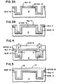
- Figure 1 of the present application illustrates the data of the U.S. Patent, and shows that for vertical sidewall trenches, the deposited silicon dioxide forms negative sloping sidewalls and, thus, voids.
- U.S. Patent No. 4,104,086 uses tapered trench sidewalls to control the depth of isolation oxide voids relative to the substrate surface in a silicon substrate which has a highly doped near-surface region.
- a process of the kind specified hereinabove is known from U.S. Patent No. 4,404,735, which discloses a process for forming trench isolation structures. Initially, dry etching such as plasma etching, reactive sputter etching or ion beam etching is used to form a trench. The trench is then covered with a thin layer of deposited silicon dioxide which is formed to a thickness of between 500 to 1,000 Angstroms to prevent substrate heating by the subsequent laser reflow process, prevent doping of the substrate from the isolation layer, and to isolate the silicon isolation layer from the substrate. Next, a CVD layer is formed to a thickness which is less than the trench depth and less than one-half the trench width using silicon or doped glass (phosphosilicate glass, PSG).
- silicon or doped glass phosphosilicate glass, PSG
- the PSG/silicon is subsequently reflowed by laser heating.
- the known process is a laser reflow process for filling narrow trenches from a thin silicon or PSG layer.
- the trench-filling layer is formed to an initial shallow thickness within the trench and laser heating is used to redistribute material from outside the trenches into the trenches.
- the 500 to 1,000 Angstrom thickness of the blocking silicon dioxide layer is critical in that a minimum thickness is required to perform the heat-shielding and dopant-blocking functions, while presumably, a maximum thickness is necessary for consistency with the stated depth and width dimensions.
- the dopant-blocking function of the silicon dioxide layer has limited effectiveness at the relatively high temperatures which may be utilized in processing the substrate to form devices therein.
- a trench isolation technology utilizes the reflow characteristics of doped silica glass at elevated temperatures to compensate for the tendency to form voids in the trenches of varying dimensions which are required for small geometry, high-density, monolithic integrated circuits.
- the process thereby provides a high-quality, void-free planar trench isolation structure.
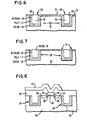
- the preliminary formation of a silicon nitride barrier layer prevents doping and oxidation of the underlying structure, particularly the semiconductor substrate; an underlying polysilicon layer provides an etch-stop during the oxide planarization etch- back; and an underlying silicon oxide layer decreases stress in the four-layer composite trench structure.
- the process enables the use of vertical sidewalls in trench structures of various widths. These vertical sidewalls minimize the effective wafer area allocated to the trenches.
- the process results in a planar wafer surface suitable for use with high resolution photolithography. Foremost, these objectives are obtained through the use of conventional fabrication techniques, and without imposing elaborate trench shape or dimensional controls.
- the silicon nitride barrier layer 18 is then formed to a thickness of 100 to 250 nm (1,000 to 2,500 Angstroms) on the polysilicon layer 17, preferably by low pressure chemical vapor deposition using silane and ammonia and a reaction temperature of about 800°C.
- the silicon nitride layer 18 provides a barrier to doping and oxidation of the underlying structure, particularly substrate 10, during subsequent processing. Thereby, silicon nitride layer 18 permits formation and reflow of the . doped isolation oxide and subsequent outgassing of the dopant in the isolation oxide without. affecting the substrate or polysilicon or the rest of the underlying structure.
- the resulting silicon dioxide layer 19 includes voids 21-21, which is typical when silicon dioxide or other dielectric layers are formed in deep trenches.
- the voids occur because the arrival angles of the depositing silicon dioxide at the bottom 22 and sidewalls 14-14 of the trench are small in comparison to the arrival angle at the top edges 23-23 of the trench. This produces relatively low deposition growth rates at the bottom and sides in comparison to the top and edge.
- the deposition rate differential produces the negatively sloped sidewalls which are evidenced by the data of Figure 1, with the result that the fast growing oxide in the edge regions 23-23 closes up the opening of the trench before the bottom regions are filled.
- the resulting voids 21-21 are not filled in by subsequent oxide growth or by the application of planarization materials such as polymer layers.
- the voids would be exposed during the subsequent etchback which is used to planarize the doped glass, creating an open receptacle for process chemical or impurities and allowing subsequently deposited metallization to flow into the voids and short other devices and components along the trench.
- the fabrication process for the poly-nitride- oxide composite of Figure 3A is similar to that described relative to the nitride-poly-oxide composition of Figure 3 with the exception that the nitride 48 is under the poly etch-stop layer 47 and thus typically cannot be removed during the etch back of glass 19. Instead, the etching sequence is glass 19, poly 47, and then nitride 48.
- the poly 47, nitride 48 and oxide 16 of Figure 3A perform the same functions-etch-stop, oxidation and dopant blocking, and stress relief-as do the poly 17, nitride 18 and oxide 16 of Figure 3.
- a poly-nitride-poly-oxide sequence of layers is used.
- the outermost poly layer 47 acts as a barrier for the nitride 18 to eliminate any nitride reaction with the glass isolation layer 19, e.g., during the oxide reflow.
- oxidation of the poly 47 helps fill in and level the trench structures.
- the nitride 18 in turn blocks oxidation of the innermost poly layer 17 and thereby limits any poly consumption during the reflow step to the outermost poly layer 47.
- the nitride layer 18 preserves the innermost poly layer 17 and permits the use of an oxidizing ambient during reflow.
Landscapes
- Element Separation (AREA)
Abstract
Claims (11)
Applications Claiming Priority (2)
| Application Number | Priority Date | Filing Date | Title |
|---|---|---|---|
| US06/667,181 US4571819A (en) | 1984-11-01 | 1984-11-01 | Method for forming trench isolation structures |
| US667181 | 1984-11-01 |
Publications (2)
| Publication Number | Publication Date |
|---|---|
| EP0200771A1 EP0200771A1 (fr) | 1986-11-12 |
| EP0200771B1 true EP0200771B1 (fr) | 1989-07-26 |
Family
ID=24677153
Family Applications (1)
| Application Number | Title | Priority Date | Filing Date |
|---|---|---|---|
| EP85905690A Expired EP0200771B1 (fr) | 1984-11-01 | 1985-10-28 | Procede de formation de zones d'isolation dans un substrat de semi-conducteurs |
Country Status (5)
| Country | Link |
|---|---|
| US (1) | US4571819A (fr) |
| EP (1) | EP0200771B1 (fr) |
| JP (1) | JPH0685413B2 (fr) |
| DE (1) | DE3571893D1 (fr) |
| WO (1) | WO1986002777A1 (fr) |
Families Citing this family (168)
| Publication number | Priority date | Publication date | Assignee | Title |
|---|---|---|---|---|
| US4604162A (en) * | 1983-06-13 | 1986-08-05 | Ncr Corporation | Formation and planarization of silicon-on-insulator structures |
| US4653177A (en) * | 1985-07-25 | 1987-03-31 | At&T Bell Laboratories | Method of making and selectively doping isolation trenches utilized in CMOS devices |
| US5462767A (en) * | 1985-09-21 | 1995-10-31 | Semiconductor Energy Laboratory Co., Ltd. | CVD of conformal coatings over a depression using alkylmetal precursors |
| US4671970A (en) * | 1986-02-05 | 1987-06-09 | Ncr Corporation | Trench filling and planarization process |
| US4666556A (en) * | 1986-05-12 | 1987-05-19 | International Business Machines Corporation | Trench sidewall isolation by polysilicon oxidation |
| US4842675A (en) * | 1986-07-07 | 1989-06-27 | Texas Instruments Incorporated | Integrated circuit isolation process |
| US4892614A (en) * | 1986-07-07 | 1990-01-09 | Texas Instruments Incorporated | Integrated circuit isolation process |
| US4755477A (en) * | 1987-03-24 | 1988-07-05 | Industrial Technology Research Institute | Overhang isolation technology |
| US4735679A (en) * | 1987-03-30 | 1988-04-05 | International Business Machines Corporation | Method of improving silicon-on-insulator uniformity |
| GB2207281B (en) * | 1987-07-24 | 1992-02-05 | Plessey Co Plc | A method of providing refilled trenches |
| US4960727A (en) * | 1987-11-17 | 1990-10-02 | Motorola, Inc. | Method for forming a dielectric filled trench |
| US4855804A (en) * | 1987-11-17 | 1989-08-08 | Motorola, Inc. | Multilayer trench isolation process and structure |
| US4871689A (en) * | 1987-11-17 | 1989-10-03 | Motorola Inc. | Multilayer trench isolation process and structure |
| US4876217A (en) * | 1988-03-24 | 1989-10-24 | Motorola Inc. | Method of forming semiconductor structure isolation regions |
| WO1990010307A1 (fr) * | 1989-02-21 | 1990-09-07 | Lam Research Corporation | Nouveau procede de depot de verre a ecoulement visco-elastique |
| US5104482A (en) * | 1989-02-21 | 1992-04-14 | Lam Research Corporation | Simultaneous glass deposition and viscoelastic flow process |
| US4952524A (en) * | 1989-05-05 | 1990-08-28 | At&T Bell Laboratories | Semiconductor device manufacture including trench formation |
| US5164218A (en) * | 1989-05-12 | 1992-11-17 | Nippon Soken, Inc. | Semiconductor device and a method for producing the same |
| CA2016449C (fr) * | 1989-07-28 | 1996-06-25 | Steven J. Hillenius | Methode d'isolement planar pour circuits integres |
| JP2822656B2 (ja) * | 1990-10-17 | 1998-11-11 | 株式会社デンソー | 半導体装置およびその製造方法 |
| JP3308556B2 (ja) * | 1991-05-08 | 2002-07-29 | 日本電気株式会社 | 半導体装置の製造方法 |
| JPH0574927A (ja) * | 1991-09-13 | 1993-03-26 | Nec Corp | 半導体装置の製造方法 |
| US5480832A (en) * | 1991-10-14 | 1996-01-02 | Nippondenso Co., Ltd. | Method for fabrication of semiconductor device |
| US5244827A (en) * | 1991-10-31 | 1993-09-14 | Sgs-Thomson Microelectronics, Inc. | Method for planarized isolation for cmos devices |
| DE69232648T2 (de) * | 1991-11-29 | 2003-02-06 | Sony Corp., Tokio/Tokyo | Verfahren zur Herstellung einer Grabenisolation mittels eines Polierschritts und Herstellungsverfahren für eine Halbleitervorrichtung |
| JP2874486B2 (ja) * | 1991-11-29 | 1999-03-24 | ソニー株式会社 | ポリッシュ工程を備えたトレンチアイソレーションの形成方法及び半導体装置の製造方法 |
| US5190889A (en) * | 1991-12-09 | 1993-03-02 | Motorola, Inc. | Method of forming trench isolation structure with germanium silicate filling |
| US5254873A (en) * | 1991-12-09 | 1993-10-19 | Motorola, Inc. | Trench structure having a germanium silicate region |
| JP3057882B2 (ja) * | 1992-03-09 | 2000-07-04 | 日本電気株式会社 | 半導体装置の製造方法 |
| US5229316A (en) * | 1992-04-16 | 1993-07-20 | Micron Technology, Inc. | Semiconductor processing method for forming substrate isolation trenches |
| US5433794A (en) * | 1992-12-10 | 1995-07-18 | Micron Technology, Inc. | Spacers used to form isolation trenches with improved corners |
| US5278103A (en) * | 1993-02-26 | 1994-01-11 | Lsi Logic Corporation | Method for the controlled formation of voids in doped glass dielectric films |
| JPH06342846A (ja) * | 1993-04-07 | 1994-12-13 | Mitsubishi Electric Corp | トレンチ分離構造を有する半導体装置およびその製造方法 |
| US5516720A (en) * | 1994-02-14 | 1996-05-14 | United Microelectronics Corporation | Stress relaxation in dielectric before metallization |
| FR2717306B1 (fr) * | 1994-03-11 | 1996-07-19 | Maryse Paoli | Procédé d'isolement de zones actives d'un substrat semi-conducteur par tranchées peu profondes, notamment étroites, et dispositif correspondant. |
| US5492858A (en) * | 1994-04-20 | 1996-02-20 | Digital Equipment Corporation | Shallow trench isolation process for high aspect ratio trenches |
| DE69524992T2 (de) * | 1994-06-08 | 2002-06-27 | Samsung Electronics Co., Ltd. | Verfahren zur Isolierung von Teilen einer Halbleitervorrichtung |
| US5459096A (en) * | 1994-07-05 | 1995-10-17 | Motorola Inc. | Process for fabricating a semiconductor device using dual planarization layers |
| US5960300A (en) * | 1994-12-20 | 1999-09-28 | Matsushita Electric Industrial Co., Ltd. | Method of manufacturing semiconductor device |
| US5616513A (en) * | 1995-06-01 | 1997-04-01 | International Business Machines Corporation | Shallow trench isolation with self aligned PSG layer |
| US6919260B1 (en) | 1995-11-21 | 2005-07-19 | Kabushiki Kaisha Toshiba | Method of manufacturing a substrate having shallow trench isolation |
| TW389999B (en) * | 1995-11-21 | 2000-05-11 | Toshiba Corp | Substrate having shallow trench isolation and method of manufacturing the same |
| KR0179807B1 (ko) * | 1995-12-30 | 1999-03-20 | 문정환 | 반도체 기억소자 제조방법 |
| US5888876A (en) * | 1996-04-09 | 1999-03-30 | Kabushiki Kaisha Toshiba | Deep trench filling method using silicon film deposition and silicon migration |
| KR0183886B1 (ko) * | 1996-06-17 | 1999-04-15 | 김광호 | 반도체장치의 트렌치 소자분리 방법 |
| US5757059A (en) * | 1996-07-30 | 1998-05-26 | International Business Machines Corporation | Insulated gate field effect transistor |
| JP3904676B2 (ja) * | 1997-04-11 | 2007-04-11 | 株式会社ルネサステクノロジ | トレンチ型素子分離構造の製造方法およびトレンチ型素子分離構造 |
| US6069058A (en) * | 1997-05-14 | 2000-05-30 | United Semiconductor Corp. | Shallow trench isolation for semiconductor devices |
| JPH10321716A (ja) * | 1997-05-16 | 1998-12-04 | Texas Instr Japan Ltd | 半導体装置及びその製造方法 |
| US6306722B1 (en) * | 1999-05-03 | 2001-10-23 | United Microelectronics Corp. | Method for fabricating shallow trench isolation structure |
| US6118167A (en) * | 1997-11-13 | 2000-09-12 | National Semiconductor Corporation | Polysilicon coated nitride-lined shallow trench |
| JP2002510139A (ja) | 1998-01-15 | 2002-04-02 | コーネル・リサーチ・ファンデーション・インコーポレイテッド | ミクロ加工デバイスのトレンチアイソレーション |
| US6699794B1 (en) * | 1998-03-09 | 2004-03-02 | Siemens Aktiengesellschaft | Self aligned buried plate |
| KR100280106B1 (ko) * | 1998-04-16 | 2001-03-02 | 윤종용 | 트렌치 격리 형성 방법 |
| US6362064B2 (en) * | 1998-04-21 | 2002-03-26 | National Semiconductor Corporation | Elimination of walkout in high voltage trench isolated devices |
| US6146970A (en) * | 1998-05-26 | 2000-11-14 | Motorola Inc. | Capped shallow trench isolation and method of formation |
| US6074903A (en) * | 1998-06-16 | 2000-06-13 | Siemens Aktiengesellschaft | Method for forming electrical isolation for semiconductor devices |
| JP2000031264A (ja) | 1998-07-08 | 2000-01-28 | Mitsubishi Electric Corp | 半導体装置およびその製造方法 |
| KR100287181B1 (ko) * | 1998-09-21 | 2001-04-16 | 윤종용 | 트렌치소자분리영역을갖는반도체소자및그제조방법 |
| KR100292616B1 (ko) * | 1998-10-09 | 2001-07-12 | 윤종용 | 트렌치격리의제조방법 |
| JP3661444B2 (ja) * | 1998-10-28 | 2005-06-15 | 株式会社ルネサステクノロジ | 半導体装置、半導体ウエハ、半導体モジュールおよび半導体装置の製造方法 |
| US6200880B1 (en) * | 1998-11-16 | 2001-03-13 | United Microelectronics Corp. | Method for forming shallow trench isolation |
| US6238998B1 (en) * | 1998-11-20 | 2001-05-29 | International Business Machines Corporation | Shallow trench isolation on a silicon substrate using nitrogen implant into the side wall |
| US6037238A (en) * | 1999-01-04 | 2000-03-14 | Vanguard International Semiconductor Corporation | Process to reduce defect formation occurring during shallow trench isolation formation |
| KR100322531B1 (ko) * | 1999-01-11 | 2002-03-18 | 윤종용 | 파임방지막을 이용하는 반도체소자의 트랜치 소자분리방법 및이를 이용한 반도체소자 |
| TW400605B (en) * | 1999-01-16 | 2000-08-01 | United Microelectronics Corp | The manufacturing method of the Shallow Trench Isolation (STI) |
| KR100312943B1 (ko) * | 1999-03-18 | 2001-11-03 | 김영환 | 반도체장치 및 그의 제조방법 |
| KR100319620B1 (ko) * | 1999-05-10 | 2002-01-05 | 김영환 | 반도체 소자의 격리구조 및 그 제조방법 |
| US6365489B1 (en) * | 1999-06-15 | 2002-04-02 | Micron Technology, Inc. | Creation of subresolution features via flow characteristics |
| KR100338767B1 (ko) * | 1999-10-12 | 2002-05-30 | 윤종용 | 트렌치 소자분리 구조와 이를 갖는 반도체 소자 및 트렌치 소자분리 방법 |
| JP2001118919A (ja) * | 1999-10-15 | 2001-04-27 | Seiko Epson Corp | 半導体装置およびその製造方法 |
| KR100308793B1 (ko) * | 1999-10-18 | 2001-11-02 | 윤종용 | 반도체 소자 제조방법 |
| US20020071169A1 (en) | 2000-02-01 | 2002-06-13 | Bowers John Edward | Micro-electro-mechanical-system (MEMS) mirror device |
| US6753638B2 (en) | 2000-02-03 | 2004-06-22 | Calient Networks, Inc. | Electrostatic actuator for micromechanical systems |
| US6583025B2 (en) * | 2000-07-10 | 2003-06-24 | Samsung Electronics Co., Ltd. | Method of forming a trench isolation structure comprising annealing the oxidation barrier layer thereof in a furnace |
| US6482075B1 (en) * | 2000-09-27 | 2002-11-19 | Lsi Logic Corporation | Process for planarizing an isolation structure in a substrate |
| US6825967B1 (en) | 2000-09-29 | 2004-11-30 | Calient Networks, Inc. | Shaped electrodes for micro-electro-mechanical-system (MEMS) devices to improve actuator performance and methods for fabricating the same |
| JP2003007872A (ja) * | 2001-06-27 | 2003-01-10 | Mitsubishi Electric Corp | 半導体装置およびその製造方法 |
| US6544863B1 (en) | 2001-08-21 | 2003-04-08 | Calient Networks, Inc. | Method of fabricating semiconductor wafers having multiple height subsurface layers |
| JP4139105B2 (ja) * | 2001-12-20 | 2008-08-27 | 株式会社ルネサステクノロジ | 半導体装置の製造方法 |
| DE10200678B4 (de) * | 2002-01-10 | 2006-05-11 | Infineon Technologies Ag | Verfahren zum Bearbeiten eines Substrats zum Ausbilden einer Struktur |
| US7728339B1 (en) | 2002-05-03 | 2010-06-01 | Calient Networks, Inc. | Boundary isolation for microelectromechanical devices |
| KR100461330B1 (ko) * | 2002-07-19 | 2004-12-14 | 주식회사 하이닉스반도체 | 반도체 소자의 sti 형성공정 |
| US6828211B2 (en) * | 2002-10-01 | 2004-12-07 | Taiwan Semiconductor Manufacturing Co., Ltd. | Shallow trench filled with two or more dielectrics for isolation and coupling or for stress control |
| JP4135564B2 (ja) * | 2002-11-12 | 2008-08-20 | 株式会社デンソー | 半導体基板およびその製造方法 |
| KR100513799B1 (ko) * | 2003-06-30 | 2005-09-13 | 주식회사 하이닉스반도체 | 트렌치형 소자분리막을 구비한 반도체 소자의 제조 방법 |
| KR100923192B1 (ko) * | 2004-03-16 | 2009-10-22 | 가부시키가이샤 아이에이치아이 | 반도체 장치의 제조 방법 |
| KR100614655B1 (ko) * | 2005-01-13 | 2006-08-22 | 삼성전자주식회사 | 반도체 장치의 소자분리막을 형성하는 방법 |
| US7141486B1 (en) | 2005-06-15 | 2006-11-28 | Agere Systems Inc. | Shallow trench isolation structures comprising a graded doped sacrificial silicon dioxide material and a method for forming shallow trench isolation structures |
| US7279377B2 (en) * | 2005-08-10 | 2007-10-09 | Micron Technology, Inc. | Method and structure for shallow trench isolation during integrated circuit device manufacture |
| KR100677998B1 (ko) * | 2005-09-30 | 2007-02-02 | 동부일렉트로닉스 주식회사 | 반도체 소자의 셸로우 트렌치 소자분리막 제조 방법 |
| US7910491B2 (en) * | 2008-10-16 | 2011-03-22 | Applied Materials, Inc. | Gapfill improvement with low etch rate dielectric liners |
| US8563090B2 (en) * | 2008-10-16 | 2013-10-22 | Applied Materials, Inc. | Boron film interface engineering |
| KR101608902B1 (ko) * | 2009-11-12 | 2016-04-05 | 삼성전자주식회사 | 소자 분리 구조물을 갖는 반도체 소자 |
| US9324576B2 (en) | 2010-05-27 | 2016-04-26 | Applied Materials, Inc. | Selective etch for silicon films |
| US8741778B2 (en) | 2010-12-14 | 2014-06-03 | Applied Materials, Inc. | Uniform dry etch in two stages |
| US8771539B2 (en) | 2011-02-22 | 2014-07-08 | Applied Materials, Inc. | Remotely-excited fluorine and water vapor etch |
| US9064815B2 (en) | 2011-03-14 | 2015-06-23 | Applied Materials, Inc. | Methods for etch of metal and metal-oxide films |
| US8999856B2 (en) | 2011-03-14 | 2015-04-07 | Applied Materials, Inc. | Methods for etch of sin films |
| US8771536B2 (en) | 2011-08-01 | 2014-07-08 | Applied Materials, Inc. | Dry-etch for silicon-and-carbon-containing films |
| US8679982B2 (en) | 2011-08-26 | 2014-03-25 | Applied Materials, Inc. | Selective suppression of dry-etch rate of materials containing both silicon and oxygen |
| US8679983B2 (en) | 2011-09-01 | 2014-03-25 | Applied Materials, Inc. | Selective suppression of dry-etch rate of materials containing both silicon and nitrogen |
| US8927390B2 (en) | 2011-09-26 | 2015-01-06 | Applied Materials, Inc. | Intrench profile |
| US8808563B2 (en) | 2011-10-07 | 2014-08-19 | Applied Materials, Inc. | Selective etch of silicon by way of metastable hydrogen termination |
| WO2013070436A1 (fr) | 2011-11-08 | 2013-05-16 | Applied Materials, Inc. | Procédés de réduction de dislocation de substrat durant un traitement de remplissage d'intervalle |
| US9142400B1 (en) | 2012-07-17 | 2015-09-22 | Stc.Unm | Method of making a heteroepitaxial layer on a seed area |
| US9373517B2 (en) | 2012-08-02 | 2016-06-21 | Applied Materials, Inc. | Semiconductor processing with DC assisted RF power for improved control |
| US9034770B2 (en) | 2012-09-17 | 2015-05-19 | Applied Materials, Inc. | Differential silicon oxide etch |
| US9023734B2 (en) | 2012-09-18 | 2015-05-05 | Applied Materials, Inc. | Radical-component oxide etch |
| US9390937B2 (en) | 2012-09-20 | 2016-07-12 | Applied Materials, Inc. | Silicon-carbon-nitride selective etch |
| US9132436B2 (en) | 2012-09-21 | 2015-09-15 | Applied Materials, Inc. | Chemical control features in wafer process equipment |
| US8765574B2 (en) | 2012-11-09 | 2014-07-01 | Applied Materials, Inc. | Dry etch process |
| US8969212B2 (en) | 2012-11-20 | 2015-03-03 | Applied Materials, Inc. | Dry-etch selectivity |
| US9064816B2 (en) | 2012-11-30 | 2015-06-23 | Applied Materials, Inc. | Dry-etch for selective oxidation removal |
| US8980763B2 (en) | 2012-11-30 | 2015-03-17 | Applied Materials, Inc. | Dry-etch for selective tungsten removal |
| US9111877B2 (en) | 2012-12-18 | 2015-08-18 | Applied Materials, Inc. | Non-local plasma oxide etch |
| US8921234B2 (en) | 2012-12-21 | 2014-12-30 | Applied Materials, Inc. | Selective titanium nitride etching |
| US9018108B2 (en) | 2013-01-25 | 2015-04-28 | Applied Materials, Inc. | Low shrinkage dielectric films |
| US10256079B2 (en) | 2013-02-08 | 2019-04-09 | Applied Materials, Inc. | Semiconductor processing systems having multiple plasma configurations |
| US9362130B2 (en) | 2013-03-01 | 2016-06-07 | Applied Materials, Inc. | Enhanced etching processes using remote plasma sources |
| US9040422B2 (en) | 2013-03-05 | 2015-05-26 | Applied Materials, Inc. | Selective titanium nitride removal |
| US8801952B1 (en) | 2013-03-07 | 2014-08-12 | Applied Materials, Inc. | Conformal oxide dry etch |
| US10170282B2 (en) | 2013-03-08 | 2019-01-01 | Applied Materials, Inc. | Insulated semiconductor faceplate designs |
| US20140271097A1 (en) | 2013-03-15 | 2014-09-18 | Applied Materials, Inc. | Processing systems and methods for halide scavenging |
| US8895449B1 (en) | 2013-05-16 | 2014-11-25 | Applied Materials, Inc. | Delicate dry clean |
| US9114438B2 (en) | 2013-05-21 | 2015-08-25 | Applied Materials, Inc. | Copper residue chamber clean |
| US9493879B2 (en) | 2013-07-12 | 2016-11-15 | Applied Materials, Inc. | Selective sputtering for pattern transfer |
| US9773648B2 (en) | 2013-08-30 | 2017-09-26 | Applied Materials, Inc. | Dual discharge modes operation for remote plasma |
| US8956980B1 (en) | 2013-09-16 | 2015-02-17 | Applied Materials, Inc. | Selective etch of silicon nitride |
| JP5916676B2 (ja) * | 2013-09-20 | 2016-05-11 | 株式会社東芝 | インクジェットヘッド、インクジェット記録装置及びインクジェットヘッドの製造方法 |
| US8951429B1 (en) | 2013-10-29 | 2015-02-10 | Applied Materials, Inc. | Tungsten oxide processing |
| US9576809B2 (en) | 2013-11-04 | 2017-02-21 | Applied Materials, Inc. | Etch suppression with germanium |
| US9236265B2 (en) | 2013-11-04 | 2016-01-12 | Applied Materials, Inc. | Silicon germanium processing |
| US9520303B2 (en) | 2013-11-12 | 2016-12-13 | Applied Materials, Inc. | Aluminum selective etch |
| US9245762B2 (en) | 2013-12-02 | 2016-01-26 | Applied Materials, Inc. | Procedure for etch rate consistency |
| US9117855B2 (en) | 2013-12-04 | 2015-08-25 | Applied Materials, Inc. | Polarity control for remote plasma |
| US9287095B2 (en) | 2013-12-17 | 2016-03-15 | Applied Materials, Inc. | Semiconductor system assemblies and methods of operation |
| US9263278B2 (en) | 2013-12-17 | 2016-02-16 | Applied Materials, Inc. | Dopant etch selectivity control |
| US9190293B2 (en) | 2013-12-18 | 2015-11-17 | Applied Materials, Inc. | Even tungsten etch for high aspect ratio trenches |
| US9287134B2 (en) | 2014-01-17 | 2016-03-15 | Applied Materials, Inc. | Titanium oxide etch |
| US9564357B2 (en) * | 2014-01-24 | 2017-02-07 | Taiwan Semiconductor Manufacturing Company Limited | Method of forming semiconductor device using etch stop layer |
| US9396989B2 (en) | 2014-01-27 | 2016-07-19 | Applied Materials, Inc. | Air gaps between copper lines |
| US9293568B2 (en) | 2014-01-27 | 2016-03-22 | Applied Materials, Inc. | Method of fin patterning |
| US9385028B2 (en) | 2014-02-03 | 2016-07-05 | Applied Materials, Inc. | Air gap process |
| US9299575B2 (en) | 2014-03-17 | 2016-03-29 | Applied Materials, Inc. | Gas-phase tungsten etch |
| US9299537B2 (en) | 2014-03-20 | 2016-03-29 | Applied Materials, Inc. | Radial waveguide systems and methods for post-match control of microwaves |
| US9299538B2 (en) | 2014-03-20 | 2016-03-29 | Applied Materials, Inc. | Radial waveguide systems and methods for post-match control of microwaves |
| US9136273B1 (en) | 2014-03-21 | 2015-09-15 | Applied Materials, Inc. | Flash gate air gap |
| US9903020B2 (en) | 2014-03-31 | 2018-02-27 | Applied Materials, Inc. | Generation of compact alumina passivation layers on aluminum plasma equipment components |
| US9309598B2 (en) | 2014-05-28 | 2016-04-12 | Applied Materials, Inc. | Oxide and metal removal |
| US9847289B2 (en) | 2014-05-30 | 2017-12-19 | Applied Materials, Inc. | Protective via cap for improved interconnect performance |
| US9406523B2 (en) | 2014-06-19 | 2016-08-02 | Applied Materials, Inc. | Highly selective doped oxide removal method |
| US9378969B2 (en) | 2014-06-19 | 2016-06-28 | Applied Materials, Inc. | Low temperature gas-phase carbon removal |
| US9425058B2 (en) | 2014-07-24 | 2016-08-23 | Applied Materials, Inc. | Simplified litho-etch-litho-etch process |
| US9378978B2 (en) | 2014-07-31 | 2016-06-28 | Applied Materials, Inc. | Integrated oxide recess and floating gate fin trimming |
| US9496167B2 (en) | 2014-07-31 | 2016-11-15 | Applied Materials, Inc. | Integrated bit-line airgap formation and gate stack post clean |
| US9159606B1 (en) | 2014-07-31 | 2015-10-13 | Applied Materials, Inc. | Metal air gap |
| US9165786B1 (en) | 2014-08-05 | 2015-10-20 | Applied Materials, Inc. | Integrated oxide and nitride recess for better channel contact in 3D architectures |
| US9659753B2 (en) | 2014-08-07 | 2017-05-23 | Applied Materials, Inc. | Grooved insulator to reduce leakage current |
| US9553102B2 (en) | 2014-08-19 | 2017-01-24 | Applied Materials, Inc. | Tungsten separation |
| US9355856B2 (en) | 2014-09-12 | 2016-05-31 | Applied Materials, Inc. | V trench dry etch |
| US20160225652A1 (en) | 2015-02-03 | 2016-08-04 | Applied Materials, Inc. | Low temperature chuck for plasma processing systems |
| TWI638401B (zh) * | 2017-07-06 | 2018-10-11 | 旺宏電子股份有限公司 | 半導體元件及其製造方法 |
| US10580789B2 (en) | 2017-07-10 | 2020-03-03 | Macronix International Co., Ltd. | Semiconductor device having etching control layer in substrate and method of fabricating the same |
| CN109256389B (zh) * | 2017-07-13 | 2021-06-11 | 旺宏电子股份有限公司 | 半导体元件及其制造方法 |
| US11067750B2 (en) | 2019-01-28 | 2021-07-20 | Cisco Technology, Inc. | Silicon photonics platform with integrated oxide trench edge coupler structure |
| CN110517985B (zh) * | 2019-09-03 | 2021-08-17 | 中国电子科技集团公司第五十八研究所 | 一种提高高压器件抗辐照性能的方法 |
| US12103843B2 (en) | 2021-01-20 | 2024-10-01 | Calient.Ai Inc. | MEMS mirror arrays with reduced crosstalk |
Citations (3)
| Publication number | Priority date | Publication date | Assignee | Title |
|---|---|---|---|---|
| US4404735A (en) * | 1980-05-14 | 1983-09-20 | Fujitsu Limited | Method for manufacturing a field isolation structure for a semiconductor device |
| EP0097789A2 (fr) * | 1982-06-30 | 1984-01-11 | International Business Machines Corporation | Procédé pour le remplissage avec silicium de tranchées dans des substrats semi-conducteurs |
| EP0104765A2 (fr) * | 1982-08-24 | 1984-04-04 | Nippon Telegraph And Telephone Corporation | Structure de substrat pour dispositif semi-conducteur et procédé pour la fabrication du substrat |
Family Cites Families (12)
| Publication number | Priority date | Publication date | Assignee | Title |
|---|---|---|---|---|
| US4104086A (en) * | 1977-08-15 | 1978-08-01 | International Business Machines Corporation | Method for forming isolated regions of silicon utilizing reactive ion etching |
| US4307180A (en) * | 1980-08-22 | 1981-12-22 | International Business Machines Corp. | Process of forming recessed dielectric regions in a monocrystalline silicon substrate |
| US4356211A (en) * | 1980-12-19 | 1982-10-26 | International Business Machines Corporation | Forming air-dielectric isolation regions in a monocrystalline silicon substrate by differential oxidation of polysilicon |
| JPS57113248A (en) * | 1980-12-29 | 1982-07-14 | Fujitsu Ltd | Manufacture of semiconductor device |
| JPS57113250A (en) * | 1980-12-29 | 1982-07-14 | Fujitsu Ltd | Semiconductor device |
| JPS57133646A (en) * | 1981-02-12 | 1982-08-18 | Fujitsu Ltd | Semiconductor integrated circuit device and manufacture thereof |
| JPS57204133A (en) * | 1981-06-10 | 1982-12-14 | Hitachi Ltd | Manufacture of semiconductor integrated circuit |
| JPS5848936A (ja) * | 1981-09-10 | 1983-03-23 | Fujitsu Ltd | 半導体装置の製造方法 |
| US4385975A (en) * | 1981-12-30 | 1983-05-31 | International Business Machines Corp. | Method of forming wide, deep dielectric filled isolation trenches in the surface of a silicon semiconductor substrate |
| NL8200782A (nl) * | 1982-02-26 | 1983-09-16 | Philips Nv | Werkwijze ter vervaardiging van een halfgeleiderinrichting en halfgeleiderinrichting vervaardigd door toepassing van deze werkwijze. |
| JPS5950540A (ja) * | 1982-09-17 | 1984-03-23 | Oki Electric Ind Co Ltd | 半導体装置の製造方法 |
| US4519128A (en) * | 1983-10-05 | 1985-05-28 | International Business Machines Corporation | Method of making a trench isolated device |
-
1984
- 1984-11-01 US US06/667,181 patent/US4571819A/en not_active Expired - Lifetime
-
1985
- 1985-10-28 DE DE8585905690T patent/DE3571893D1/de not_active Expired
- 1985-10-28 EP EP85905690A patent/EP0200771B1/fr not_active Expired
- 1985-10-28 JP JP60505028A patent/JPH0685413B2/ja not_active Expired - Fee Related
- 1985-10-28 WO PCT/US1985/002119 patent/WO1986002777A1/fr not_active Ceased
Patent Citations (3)
| Publication number | Priority date | Publication date | Assignee | Title |
|---|---|---|---|---|
| US4404735A (en) * | 1980-05-14 | 1983-09-20 | Fujitsu Limited | Method for manufacturing a field isolation structure for a semiconductor device |
| EP0097789A2 (fr) * | 1982-06-30 | 1984-01-11 | International Business Machines Corporation | Procédé pour le remplissage avec silicium de tranchées dans des substrats semi-conducteurs |
| EP0104765A2 (fr) * | 1982-08-24 | 1984-04-04 | Nippon Telegraph And Telephone Corporation | Structure de substrat pour dispositif semi-conducteur et procédé pour la fabrication du substrat |
Also Published As
| Publication number | Publication date |
|---|---|
| JPH0685413B2 (ja) | 1994-10-26 |
| EP0200771A1 (fr) | 1986-11-12 |
| JPS62500762A (ja) | 1987-03-26 |
| DE3571893D1 (en) | 1989-08-31 |
| WO1986002777A1 (fr) | 1986-05-09 |
| US4571819A (en) | 1986-02-25 |
Similar Documents
| Publication | Publication Date | Title |
|---|---|---|
| EP0200771B1 (fr) | Procede de formation de zones d'isolation dans un substrat de semi-conducteurs | |
| US4656497A (en) | Trench isolation structures | |
| US5902127A (en) | Methods for forming isolation trenches including doped silicon oxide | |
| US4952524A (en) | Semiconductor device manufacture including trench formation | |
| US5801082A (en) | Method for making improved shallow trench isolation with dielectric studs for semiconductor integrated circuits | |
| US5721172A (en) | Self-aligned polish stop layer hard masking method for forming planarized aperture fill layers | |
| US6194283B1 (en) | High density trench fill due to new spacer fill method including isotropically etching silicon nitride spacers | |
| US7402473B2 (en) | Semiconductor device and process for producing the same | |
| EP0459397B1 (fr) | Procédé de fabricaiton d'un dispositif semi-conducteur comportant une rainure pour isoler des composants | |
| US6069058A (en) | Shallow trench isolation for semiconductor devices | |
| US6265302B1 (en) | Partially recessed shallow trench isolation method for fabricating borderless contacts | |
| US7372102B2 (en) | Structure having a shallow trench-deep trench isolation region for a BiCMOS/CMOS technology | |
| US6174785B1 (en) | Method of forming trench isolation region for semiconductor device | |
| US6001706A (en) | Method for making improved shallow trench isolation for semiconductor integrated circuits | |
| US8173517B2 (en) | Method for forming a self-aligned isolation structure utilizing sidewall spacers as an etch mask and remaining as a portion of the isolation structure | |
| US5413953A (en) | Method for planarizing an insulator on a semiconductor substrate using ion implantation | |
| EP0813240A1 (fr) | Améliorations dans ou relatives aux dispositifs semi-conducteurs | |
| US5496765A (en) | Method for manufacturing an insulating trench in a substrate for smart-power technologies | |
| JPH0680724B2 (ja) | 絶縁分離のcmos fet集積装置の製造方法 | |
| US6432797B1 (en) | Simplified method to reduce or eliminate STI oxide divots | |
| US6893937B1 (en) | Method for preventing borderless contact to well leakage | |
| US6433400B1 (en) | Semiconductor fabrication employing barrier atoms incorporated at the edges of a trench isolation structure | |
| US7074692B2 (en) | Method for reducing a short channel effect for NMOS devices in SOI circuits | |
| US6602759B2 (en) | Shallow trench isolation for thin silicon/silicon-on-insulator substrates by utilizing polysilicon | |
| US5994718A (en) | Trench refill with selective polycrystalline materials |
Legal Events
| Date | Code | Title | Description |
|---|---|---|---|
| PUAI | Public reference made under article 153(3) epc to a published international application that has entered the european phase |
Free format text: ORIGINAL CODE: 0009012 |
|
| AK | Designated contracting states |
Kind code of ref document: A1 Designated state(s): DE GB NL |
|
| 17P | Request for examination filed |
Effective date: 19861014 |
|
| DET | De: translation of patent claims | ||
| 17Q | First examination report despatched |
Effective date: 19880509 |
|
| GRAA | (expected) grant |
Free format text: ORIGINAL CODE: 0009210 |
|
| AK | Designated contracting states |
Kind code of ref document: B1 Designated state(s): DE GB NL |
|
| REF | Corresponds to: |
Ref document number: 3571893 Country of ref document: DE Date of ref document: 19890831 |
|
| PLBE | No opposition filed within time limit |
Free format text: ORIGINAL CODE: 0009261 |
|
| STAA | Information on the status of an ep patent application or granted ep patent |
Free format text: STATUS: NO OPPOSITION FILED WITHIN TIME LIMIT |
|
| 26N | No opposition filed | ||
| REG | Reference to a national code |
Ref country code: GB Ref legal event code: 732E |
|
| NLS | Nl: assignments of ep-patents |
Owner name: NCR INTERNATIONAL INC. TE DAYTON, OHIO, VER. ST. V |
|
| NLT1 | Nl: modifications of names registered in virtue of documents presented to the patent office pursuant to art. 16 a, paragraph 1 |
Owner name: AT&T GLOBAL INFORMATION SOLUTIONS INTERNATIONAL IN |
|
| REG | Reference to a national code |
Ref country code: GB Ref legal event code: 732E |
|
| REG | Reference to a national code |
Ref country code: GB Ref legal event code: 732E |
|
| NLS | Nl: assignments of ep-patents |
Owner name: AT&T GLOBAL INFORMATION SOLUTIONS INTERNATIONAL IN |
|
| NLS | Nl: assignments of ep-patents |
Owner name: AT&T GLOBAL INFORMATION SOLUTIONS INTERNATIONAL IN |
|
| NLT1 | Nl: modifications of names registered in virtue of documents presented to the patent office pursuant to art. 16 a, paragraph 1 |
Owner name: NCR INTERNATIONAL, INC;HYUNDAI ELECTRONICS AMERICA |
|
| NLT1 | Nl: modifications of names registered in virtue of documents presented to the patent office pursuant to art. 16 a, paragraph 1 |
Owner name: NCR INTERNATIONAL, INC;HYUNDAI ELECTRONICS AMERICA |
|
| REG | Reference to a national code |
Ref country code: GB Ref legal event code: IF02 |
|
| PGFP | Annual fee paid to national office [announced via postgrant information from national office to epo] |
Ref country code: NL Payment date: 20041003 Year of fee payment: 20 |
|
| PGFP | Annual fee paid to national office [announced via postgrant information from national office to epo] |
Ref country code: DE Payment date: 20041021 Year of fee payment: 20 |
|
| PGFP | Annual fee paid to national office [announced via postgrant information from national office to epo] |
Ref country code: GB Payment date: 20041027 Year of fee payment: 20 |
|
| NLS | Nl: assignments of ep-patents |
Owner name: HYUNDAI ELECTRONICS AMERICA Owner name: NCR INTERNATIONAL, INC Owner name: HYNIX SEMICONDUCTOR INC. |
|
| NLT1 | Nl: modifications of names registered in virtue of documents presented to the patent office pursuant to art. 16 a, paragraph 1 |
Owner name: NCR INTERNATIONAL, INC Owner name: HYNIX SEMICONDUCTOR AMERICA INC. |
|
| REG | Reference to a national code |
Ref country code: GB Ref legal event code: 732E |
|
| PG25 | Lapsed in a contracting state [announced via postgrant information from national office to epo] |
Ref country code: GB Free format text: LAPSE BECAUSE OF EXPIRATION OF PROTECTION Effective date: 20051027 |
|
| PG25 | Lapsed in a contracting state [announced via postgrant information from national office to epo] |
Ref country code: NL Free format text: LAPSE BECAUSE OF EXPIRATION OF PROTECTION Effective date: 20051028 |
|
| REG | Reference to a national code |
Ref country code: GB Ref legal event code: PE20 |
|
| NLV7 | Nl: ceased due to reaching the maximum lifetime of a patent |
Effective date: 20051028 |