EP0034483B2 - Verfahren zur Herstellung eines Musters in einer Schicht für die Herstellung eines Kontaktloches - Google Patents
Verfahren zur Herstellung eines Musters in einer Schicht für die Herstellung eines Kontaktloches Download PDFInfo
- Publication number
- EP0034483B2 EP0034483B2 EP81300607A EP81300607A EP0034483B2 EP 0034483 B2 EP0034483 B2 EP 0034483B2 EP 81300607 A EP81300607 A EP 81300607A EP 81300607 A EP81300607 A EP 81300607A EP 0034483 B2 EP0034483 B2 EP 0034483B2
- Authority
- EP
- European Patent Office
- Prior art keywords
- hole
- layer
- insulating layer
- etching
- photoresist layer
- Prior art date
- Legal status (The legal status is an assumption and is not a legal conclusion. Google has not performed a legal analysis and makes no representation as to the accuracy of the status listed.)
- Expired
Links
Images


Classifications
-
- H10P50/73—
-
- G—PHYSICS
- G03—PHOTOGRAPHY; CINEMATOGRAPHY; ANALOGOUS TECHNIQUES USING WAVES OTHER THAN OPTICAL WAVES; ELECTROGRAPHY; HOLOGRAPHY
- G03F—PHOTOMECHANICAL PRODUCTION OF TEXTURED OR PATTERNED SURFACES, e.g. FOR PRINTING, FOR PROCESSING OF SEMICONDUCTOR DEVICES; MATERIALS THEREFOR; ORIGINALS THEREFOR; APPARATUS SPECIALLY ADAPTED THEREFOR
- G03F7/00—Photomechanical, e.g. photolithographic, production of textured or patterned surfaces, e.g. printing surfaces; Materials therefor, e.g. comprising photoresists; Apparatus specially adapted therefor
- G03F7/26—Processing photosensitive materials; Apparatus therefor
- G03F7/40—Treatment after imagewise removal, e.g. baking
-
- H10P50/283—
-
- H10W20/082—
Definitions
- the present invention relates to a process for forming a contact through hole in an insulating layer in particular of a semiconductor device such as for instance an integrated circuit (IC).
- IC integrated circuit
- an insulating layer for example an insulating layer for protection (i.e. a passivation film), over a lower conductor layer, is selectively removed to make a through hole (i.e. a via hole) and then an upper conductor layer (i.e. a conductive pattern) is formed on the insulating layer so as to come into contact with the lower conductor layer (i.e. another conductive pattern) through the through hole.
- an upper conductor layer i.e. a conductive pattern
- disconnection between the upper and lower conductor layers may occur.
- a portion of an insulating layer on a conductor layer can be selectively removed through an opening in a patterned photoresist mask by using an etching solution to form the through hole.
- An insulating layer (e.g. a phosphosilicate glass film) 1 is formed on a conductor layer (e.g. an aluminium pattern) 2 lying on another insulating layer (e.g. a silicon dioxide layer) 3 and a semiconductor substrate (e.g. a single crystalline silicon substrate) 4.
- a photoresist layer 5 is applied on the insulating layer 1 and is then exposed and developed to form a patterned mask having an opening 6 therein as illustrated in Figure 1.
- a portion of the insulating layer 1 (e.g. a phosphosilicate glass) is selectively etched by using a suitable etching solution (e.g. a mixed solution of hydrofluoric acid (HF) and nitric acid (NH0 3 )) to form a through a hole 7, as illustrated in Figure 2.
- a suitable etching solution e.g. a mixed solution of hydrofluoric acid (HF) and nitric acid (NH0 3 )
- the bottom of the through hole 7 is of a larger size, and the top of the through hole 7 is of a considerably larger size, than the size of the opening 5 in the photoresist layer 5, since the etching solution can remove the insulating layer 1 from under the edge of the photoresist layer 5 (that is, so-called undercutting or side etching occurs), and in practice overetching is carried out to ensure reliable formation of complete through holes in semiconductor device chips of a semiconductor substrate (wafer).
- a through hole 7 so formed it is possible to prevent the occurrence of cracks in an upper conductor layer; however, the formed through hole is larger than the desired size, so that the density of the conductor pattern and the integration density of the integrated circuit for example are low.
- a contact through hole can be formed by a combination of wet-etching and dry-etching, as described in prior European patent application EP-A-0 030 116, which belongs to the state of the art according to Art. 54(3) EPC.
- an exposed portion of the insulating layer 1 ( Figure 1) is wet-etched by the etching solution through the opening 6 in the photoresist layer 5.
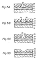
- the insulating layer 1 having a thickness of 1.0 micron, is wet-etched to form a part or preceding hole 8 having a depth of 0.7 microns, with the result that a portion of the insulating layer having a thickness of 0.3 microns remains, as illustrated in Figure 3A of the accompanying drawings, which is a partial schematic cross-sectional view.
- a conventional dry-etching e.g.
- the insulating layer 1 is further etched to complete a through hole 9, as illustrated in Figure 3B of the accompanying drawings, which is a partial schematic cross-sectional view.
- the bottom of the through hole 9 has a smaller size and the side of thet hrough hole slopes at a steeper angle as compared with the through hole 7 ( Figure 2) formed by wet-etching only.
- an etchant used for dry-etching can remove the insulating layer 1 from under the photoresist layer 5 to a slight degree, to induce a small undercut.
- the through hole 9 is slightly larger than the desired size.
- the insulating layer 1 having a thickness of 1.0 micron is wet-etched to form a part or preceding hole 10 having a depth of 0.3 microns, as illustrated in Figure 4A of the accompanying drawings, which is a partial schematic cross-sectional view. Then, in the same dry-etching apparatus the insulating layer 1 is further etched to complete a through hole 11, as illustrated in Figure 4B of the accompanying drawings, which is a partial schematic cross-sectional view.
- the formed through hole 11 has an almost vertical side surface and a short slope formed by wet-etching.
- the through hole 11 does not have a slope extending over the whole depth of the hole, cracks may occur in a conductor layer (not shown) formed over the through hole at the edge of the through hole 11, when this conductor layer is formed by a conventional process on the insulating layer 1 and on the portion of the conductor layer 2 exposed in the through hole.
- a process for forming a contact through hole in an insulating layer comprising the steps of; forming a patterned photoresist layer on the insulating layer; dry etching part way through the insulating layer, using the photoresist layer as a mask to form a part or preceding hole; and wet-etching the insulating layer using the photoresist layer as a mask, to complete the through hole.
- a process for forming a through hole comprising the steps of: forming a patterned photoresist on an insulating layer; wet-etching completely through the insulating layer, using the photoresist layer as a mask, to form a hole; heating the photoresist layer to bend the end portion of the photoresist layer around the hole; and etching a layer of electrode material provided under said insulating layer using the photoresist layer as a mask.
- a process for forming a contact through hole in an insulating layer disposed on a first conductor layer comprises the steps of forming on the insulating layer a patterned photoresist layer having an opening therein corresponding to the desired through hole; wet-etching part way through the insulating layer, using the photoresist layer as a mask, to form a part or preceding hole that has sloping sides and undercuts the end portion of the photoresist layer; heating the photoresist layer at a temperature under the softening point of the photoresist to bend the end portion of the photoresist layer around the part or preceding hole so that the said end portion does not come into contact with the slope of the part or preceding hole; and dry etching the insulating layer, using the photoresist layer as a mask, to complete the through hole with sloping sides.
- An embodiment of the present invention can provide a process for forming a contact through hole having a slope such as to prevent cracks from occurring in a conductor layer to be formed on the slope.
- An embodiment of the present invention can facilitate a density increase in an integrated in an circuit of a semiconductor device by providing for the formation of a contact through hole accurately to a desire side.
- An embodiment of the present invention provides a process for forming a throughhole, for the establishment of a connection between an upper conductor layer and a lower conductor layer, in an insulating layer between the upper and lower conductor layers. Since heating bends the end portion of the photoresist layer to such an extent that the end portion does not come into contact with the side surface of the part or preceding hole, the final through hole with sloped side surface can be formed by dry-etching without any enlargement of the top plane size of the part or preceding hole.
- a first insulating layer e.g. a silicon dioxide layer
- the semiconductor substrate has active elements and passive elements as integrated circuit elements.
- a first conductor layer 23 made of metal (e.g. aluminium) and having a desired pattern is formed on the first insulating layer 22 by a conventional process (e.g. vapour deposition and then photoetching).
- a second insulating layer 24 of phosphosilicate glass (PSG) having a thickness in the range of from 0.8 to 1.2 microns (e.g. approximately 1.0 micron) is formed on the first conductor layer 23.
- silicon dioxide Si0 2
- silicon nitride Si 3 N 4
- BSG borosilicate glass
- a positive type photoresist layer 25 having a thickness in the range of from 1.0 to 2.0 microns (e.g. approximately 1.5 microns) is coated on the second insulating layer 24 and then selectively removed to make a desired opening 26.
- a portion (having a thickness in the range of from 0.5 to 0.8 microns, e.g. approximately 0.7 microns) of the second insulating layer 24 of PSG is selectively etched by an etching solution of acid ammonium fluoride and nitric acid through the opening 26 to form a part or preceding hole 27, as illustrated in Figure 5A. Since the etching solution causes a so-called undercut, the part or preceding hole 27 has a slope.
- a suitable etching solution for the insulating material e.g. a mixture of hydrofluoric acid and alcohol
- the etching solution penetrates into the interface between the photoresist layer 25 and the insulating layer 24 to generate a large undercut at the upper portion of the insulating layer.
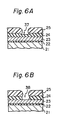
- the photoresist layer 25 is heated up to the softening point thereof so that an end portion 28 of the photoresist layer bends around the part or preceding hole 27.
- the end portion 28 should be kept off the slope of the part or preceding hole 27 (e.g. there should be no contact between the end portion 28 and the slope), as illustrated in Figure 5B.
- a positive type photoresist layer 25 of a thickness of 1.5 microns it is possible to heat the photoresist layer at a temperature in the range of 160°C to 180° C (preferably 170°C) for a period in the range from 10 minutes to 40 minutes (preferably 20 minutes).
- the heating temperature and the length of time depends on the thickness of layer 25 and the properties of the material used for layer 25.
- the exposed portion of the second insulating layer 24 is dry-etched through the window 26, for example by reactive sputter etching or plasma etching, to complete a through hole 29, as illustrated in Figure 5C.
- the dry-etching causes a smaller undercut as compared with wet-etching and the opening of the photoresist layer 25 is shaped into a truncated cone, so that the formed through hole 29 can have a slope. Since the space between the bottom plane of the photoresist layer 25 and the slope of the part or preceding hole 28 ( Figure 5B) is small, the top plane size of the part or preceding hole 28 is not enlarged by the dry-etching.
- the PSG insulating layer 24, having a part or preceding hole 0.7 microns deep can be etched by reactive sputter etching in a planar type dry-etching apparatus under the following conditions: a power density of 0.7 watt/cm 2 of a silicon substrate (e.g. 0.7 watt per square centimetre of silicon substrate), a pressure of 0.266 mbar (0.2 Torr), CHF 3 etchant gas, and an etching period of 5 minutes.
- the slope of the through hole 29 has an angle in the range of from 18° to 30°.
- CF 4 or C 2 F 6 as an etchant gas instead of CHF 3 .
- insulating layer 24 is made of Si0 2 , Si 3 N 4 or BSG, one of the above etchant gases CHF 3 , CF 4 and C 2 F 6 can be used.
- a second conductor layer 30 made of metal (e.g. aluminium) and having a desired pattern is formed on the second insulating layer 24 by a conventional process. The formed second conductor layer 30 comes into contact with the first conductor layer 23 through the through hole 29, as illustrated in Figure 5D.
- the slope of the through hole 29 can prevent cracks occurring in the second rnndiii-tnr layer 3n If a part or preceding hole 37 having a depth of 0.3 microns, instead of 0.7 microns as for part or preceding hole 27 in Figure 5A, is formed in a PSG insulating layer 24 by wet-etching and a photoresist layer 25 is heated at 170° C for 20 minutes, the end portion of the photoresist 25 comes into contact with the slope of the part or preceding hole 37, as illustrated in Figure 6A.
- the period of reactive sputter etching is relatively long and there may be a relatively large change in quality of the photoresist layer due to the dry-etching.
- the change in quality of the upper portion of the photoresist layer can cause problems in removal of the photoresist layer.
- a contact through hole is formed in accordance with a method embodying the present invention, it is possible to prevent cracks from occurring in a conductor layer on an insulating layer and on the slope of the through hole. As a result, reliability of semiconductor devices manufactured by a method embodying the present invention and the yield of good semiconductor devices as a proportion of a total number of semiconductor devices produced can be increased. Furthermore, dimensions of the top plane of a contact through hole formed in accordance with an embodiment of the present invention are not enlarged during the dry etching by a so-called undercut, so that the through hole can be accurately shaped to a predetermined size, whereby density of an integrated circuit can be increased.
- Embodiments of this invention can provide a process for forming a contact through hole in an insulating layer, for example between multi-layer conductors, in which the through hole has a slope which is essentially a straight line (as seen in cross-section) angled between 18° and 30°.
Landscapes
- Physics & Mathematics (AREA)
- General Physics & Mathematics (AREA)
- Internal Circuitry In Semiconductor Integrated Circuit Devices (AREA)
- Drying Of Semiconductors (AREA)
- Electrodes Of Semiconductors (AREA)
Claims (11)
Applications Claiming Priority (2)
| Application Number | Priority Date | Filing Date | Title |
|---|---|---|---|
| JP1685880A JPS56114319A (en) | 1980-02-14 | 1980-02-14 | Method for forming contact hole |
| JP16858/80 | 1980-02-14 |
Publications (4)
| Publication Number | Publication Date |
|---|---|
| EP0034483A2 EP0034483A2 (de) | 1981-08-26 |
| EP0034483A3 EP0034483A3 (en) | 1983-06-08 |
| EP0034483B1 EP0034483B1 (de) | 1985-10-02 |
| EP0034483B2 true EP0034483B2 (de) | 1988-11-02 |
Family
ID=11927908
Family Applications (1)
| Application Number | Title | Priority Date | Filing Date |
|---|---|---|---|
| EP81300607A Expired EP0034483B2 (de) | 1980-02-14 | 1981-02-13 | Verfahren zur Herstellung eines Musters in einer Schicht für die Herstellung eines Kontaktloches |
Country Status (4)
| Country | Link |
|---|---|
| US (1) | US4354897A (de) |
| EP (1) | EP0034483B2 (de) |
| JP (1) | JPS56114319A (de) |
| DE (1) | DE3172469D1 (de) |
Families Citing this family (27)
| Publication number | Priority date | Publication date | Assignee | Title |
|---|---|---|---|---|
| JPS5871628A (ja) * | 1981-10-23 | 1983-04-28 | Fujitsu Ltd | 半導体装置の製造方法 |
| JPS58204176A (ja) * | 1982-05-24 | 1983-11-28 | Kangiyou Denki Kiki Kk | 化学的蝕刻方法 |
| JPS59214240A (ja) * | 1983-05-09 | 1984-12-04 | Fujitsu Ltd | 半導体装置の製造方法 |
| US4425183A (en) | 1983-08-08 | 1984-01-10 | Ncr Corporation | Metal bevel process for multi-level metal semiconductor applications |
| US4508815A (en) * | 1983-11-03 | 1985-04-02 | Mostek Corporation | Recessed metallization |
| US4484979A (en) * | 1984-04-16 | 1984-11-27 | At&T Bell Laboratories | Two-step anisotropic etching process for patterning a layer without penetrating through an underlying thinner layer |
| US4719498A (en) * | 1984-05-18 | 1988-01-12 | Fujitsu Limited | Optoelectronic integrated circuit |
| IT1213230B (it) * | 1984-10-23 | 1989-12-14 | Ates Componenti Elettron | Processo planox a becco ridotto per la formazione di componenti elettronici integrati. |
| US4693783A (en) * | 1984-12-31 | 1987-09-15 | Gte Laboratories Incorporated | Method of producing interconnections in a semiconductor integrated circuit structure |
| US4645562A (en) * | 1985-04-29 | 1987-02-24 | Hughes Aircraft Company | Double layer photoresist technique for side-wall profile control in plasma etching processes |
| JPH0758718B2 (ja) * | 1985-10-18 | 1995-06-21 | 三洋電機株式会社 | 化合物半導体装置の製造方法 |
| US4702000A (en) * | 1986-03-19 | 1987-10-27 | Harris Corporation | Technique for elimination of polysilicon stringers in direct moat field oxide structure |
| US4818725A (en) * | 1986-09-15 | 1989-04-04 | Harris Corp. | Technique for forming planarized gate structure |
| JPH01255265A (ja) * | 1988-04-05 | 1989-10-12 | Nec Corp | 半導体装置の製造方法 |
| JPH02125422A (ja) * | 1988-11-02 | 1990-05-14 | Nec Corp | 半導体装置の製造方法 |
| JPH03266437A (ja) * | 1990-03-16 | 1991-11-27 | Toshiba Corp | 半導体装置の製造方法 |
| JP2932940B2 (ja) * | 1994-06-08 | 1999-08-09 | 株式会社デンソー | 薄膜抵抗体を有する半導体装置の製造方法 |
| US5746884A (en) * | 1996-08-13 | 1998-05-05 | Advanced Micro Devices, Inc. | Fluted via formation for superior metal step coverage |
| US6800210B2 (en) * | 2001-05-22 | 2004-10-05 | Reflectivity, Inc. | Method for making a micromechanical device by removing a sacrificial layer with multiple sequential etchants |
| US6559048B1 (en) * | 2001-05-30 | 2003-05-06 | Lsi Logic Corporation | Method of making a sloped sidewall via for integrated circuit structure to suppress via poisoning |
| JP4718725B2 (ja) * | 2001-07-03 | 2011-07-06 | Nec液晶テクノロジー株式会社 | 液晶表示装置の製造方法 |
| US7297639B2 (en) * | 2005-09-01 | 2007-11-20 | Micron Technology, Inc. | Methods for etching doped oxides in the manufacture of microfeature devices |
| WO2008114252A2 (en) * | 2007-03-18 | 2008-09-25 | Nanopass Technologies Ltd | Microneedle structures and corresponding production methods employing a backside wet etch |
| CN104425229A (zh) * | 2013-09-10 | 2015-03-18 | 中国科学院微电子研究所 | 鳍片制造方法 |
| CN103681306B (zh) * | 2013-12-30 | 2016-08-17 | 国家电网公司 | 一种平缓光滑侧壁形貌的氮氧硅刻蚀方法 |
| CN105225943B (zh) * | 2015-10-26 | 2018-03-06 | 中国科学院微电子研究所 | 一种氧化硅的各向异性湿法腐蚀工艺中控制倾角的方法 |
| CN113348561A (zh) * | 2018-11-26 | 2021-09-03 | 康宁股份有限公司 | 在导电层上形成图案化的绝缘层的方法及使用所述方法制造的制品 |
Family Cites Families (10)
| Publication number | Priority date | Publication date | Assignee | Title |
|---|---|---|---|---|
| US3544401A (en) * | 1967-05-16 | 1970-12-01 | Texas Instruments Inc | High depth-to-width ratio etching process |
| NL6903930A (de) * | 1969-03-14 | 1970-09-16 | ||
| JPS50134579A (de) * | 1974-04-13 | 1975-10-24 | ||
| DE2534043A1 (de) * | 1975-07-30 | 1977-02-03 | Siemens Ag | Verfahren zur herstellung von loechern in auf halbleiterkoerpern befindlichen isolatorschichten |
| DE2723499A1 (de) * | 1977-05-25 | 1978-12-07 | Licentia Gmbh | Verfahren zum herstellen eines fensters in einer isolierschicht bei halbleiteranordnungen |
| JPS6056286B2 (ja) * | 1977-11-08 | 1985-12-09 | 富士通株式会社 | 半導体装置における電極窓の形成方法 |
| DE2754066A1 (de) * | 1977-12-05 | 1979-06-13 | Siemens Ag | Herstellung einer integrierten schaltung mit abgestuften schichten aus isolations- und elektrodenmaterial |
| DE2804830A1 (de) * | 1978-02-04 | 1979-08-09 | Bosch Gmbh Robert | Verfahren zur herstellung einer halbleiteranordnung |
| US4148133A (en) * | 1978-05-08 | 1979-04-10 | Sperry Rand Corporation | Polysilicon mask for etching thick insulator |
| DE2823855A1 (de) * | 1978-05-31 | 1979-12-06 | Fujitsu Ltd | Verfahren zum herstellen einer halbleitervorrichtung |
-
1980
- 1980-02-14 JP JP1685880A patent/JPS56114319A/ja active Pending
-
1981
- 1981-02-13 EP EP81300607A patent/EP0034483B2/de not_active Expired
- 1981-02-13 DE DE8181300607T patent/DE3172469D1/de not_active Expired
- 1981-02-13 US US06/234,194 patent/US4354897A/en not_active Expired - Fee Related
Also Published As
| Publication number | Publication date |
|---|---|
| EP0034483B1 (de) | 1985-10-02 |
| EP0034483A2 (de) | 1981-08-26 |
| EP0034483A3 (en) | 1983-06-08 |
| DE3172469D1 (en) | 1985-11-07 |
| US4354897A (en) | 1982-10-19 |
| JPS56114319A (en) | 1981-09-08 |
Similar Documents
| Publication | Publication Date | Title |
|---|---|---|
| EP0034483B2 (de) | Verfahren zur Herstellung eines Musters in einer Schicht für die Herstellung eines Kontaktloches | |
| US4487652A (en) | Slope etch of polyimide | |
| US4495220A (en) | Polyimide inter-metal dielectric process | |
| JPH0135495B2 (de) | ||
| US4585515A (en) | Formation of conductive lines | |
| US6004729A (en) | Methods of improving photoresist adhesion for integrated circuit fabrication | |
| JPH06318578A (ja) | 半導体素子のコンタクトホール形成方法 | |
| JPS5916334A (ja) | ドライエツチング方法 | |
| JPH0313744B2 (de) | ||
| US5804515A (en) | Method for forming contact holes of semiconductor device | |
| JP2926790B2 (ja) | 半導体装置 | |
| KR20000044926A (ko) | 반도체 소자의 비아홀 형성 방법 | |
| JPS59232443A (ja) | 半導体装置の製造方法 | |
| US11495492B2 (en) | Method of fabricating semiconductor device | |
| JP2695919B2 (ja) | 配線パターンの形成方法 | |
| JPS6184024A (ja) | 半導体装置の製造方法 | |
| KR100373363B1 (ko) | 반도체소자의 콘택홀 형성방법 | |
| JPS59191354A (ja) | 半導体装置の製造方法 | |
| JPS6068613A (ja) | 半導体装置の製造方法 | |
| JPS6254427A (ja) | 半導体装置の製造方法 | |
| JPS5840338B2 (ja) | 半導体装置の製造法 | |
| JP3295172B2 (ja) | ドライエッチング方法及び半導体装置の製造方法 | |
| JPS58197853A (ja) | 半導体装置の製造方法 | |
| JPH0745551A (ja) | コンタクトホールの形成方法 | |
| JPH04369854A (ja) | 半導体装置及びその製造方法 |
Legal Events
| Date | Code | Title | Description |
|---|---|---|---|
| PUAI | Public reference made under article 153(3) epc to a published international application that has entered the european phase |
Free format text: ORIGINAL CODE: 0009012 |
|
| AK | Designated contracting states |
Designated state(s): DE FR GB NL |
|
| RBV | Designated contracting states (corrected) |
Designated state(s): DE FR GB NL |
|
| PUAL | Search report despatched |
Free format text: ORIGINAL CODE: 0009013 |
|
| AK | Designated contracting states |
Designated state(s): DE FR GB NL |
|
| 17P | Request for examination filed |
Effective date: 19831129 |
|
| GRAA | (expected) grant |
Free format text: ORIGINAL CODE: 0009210 |
|
| AK | Designated contracting states |
Designated state(s): DE FR GB NL |
|
| REF | Corresponds to: |
Ref document number: 3172469 Country of ref document: DE Date of ref document: 19851107 |
|
| ET | Fr: translation filed | ||
| PLBI | Opposition filed |
Free format text: ORIGINAL CODE: 0009260 |
|
| 26 | Opposition filed |
Opponent name: DEUTSCHE ITT INDUSTRIES GMBH Effective date: 19860628 |
|
| NLR1 | Nl: opposition has been filed with the epo |
Opponent name: DEUTSCHE ITT INDUSTRIES GMBH |
|
| PGFP | Annual fee paid to national office [announced via postgrant information from national office to epo] |
Ref country code: NL Payment date: 19870228 Year of fee payment: 7 |
|
| PUAH | Patent maintained in amended form |
Free format text: ORIGINAL CODE: 0009272 |
|
| STAA | Information on the status of an ep patent application or granted ep patent |
Free format text: STATUS: PATENT MAINTAINED AS AMENDED |
|
| 27A | Patent maintained in amended form |
Effective date: 19881102 |
|
| AK | Designated contracting states |
Kind code of ref document: B2 Designated state(s): DE FR GB NL |
|
| ET3 | Fr: translation filed ** decision concerning opposition | ||
| NLR2 | Nl: decision of opposition | ||
| PGFP | Annual fee paid to national office [announced via postgrant information from national office to epo] |
Ref country code: GB Payment date: 19890213 Year of fee payment: 9 |
|
| NLR3 | Nl: receipt of modified translations in the netherlands language after an opposition procedure | ||
| PG25 | Lapsed in a contracting state [announced via postgrant information from national office to epo] |
Ref country code: NL Effective date: 19890901 |
|
| NLV4 | Nl: lapsed or anulled due to non-payment of the annual fee | ||
| PG25 | Lapsed in a contracting state [announced via postgrant information from national office to epo] |
Ref country code: FR Free format text: LAPSE BECAUSE OF NON-PAYMENT OF DUE FEES Effective date: 19891027 |
|
| PG25 | Lapsed in a contracting state [announced via postgrant information from national office to epo] |
Ref country code: DE Effective date: 19891101 |
|
| REG | Reference to a national code |
Ref country code: FR Ref legal event code: ST |
|
| PG25 | Lapsed in a contracting state [announced via postgrant information from national office to epo] |
Ref country code: GB Effective date: 19900213 |
|
| GBPC | Gb: european patent ceased through non-payment of renewal fee |