JP6923284B2 - Equipment and methods for laser machining transparent workpieces using non-axisymmetric beam spots - Google Patents
Equipment and methods for laser machining transparent workpieces using non-axisymmetric beam spots Download PDFInfo
- Publication number
- JP6923284B2 JP6923284B2 JP2019517001A JP2019517001A JP6923284B2 JP 6923284 B2 JP6923284 B2 JP 6923284B2 JP 2019517001 A JP2019517001 A JP 2019517001A JP 2019517001 A JP2019517001 A JP 2019517001A JP 6923284 B2 JP6923284 B2 JP 6923284B2
- Authority
- JP
- Japan
- Prior art keywords
- laser beam
- pulsed laser
- transparent workpiece
- cross
- transparent
- Prior art date
- Legal status (The legal status is an assumption and is not a legal conclusion. Google has not performed a legal analysis and makes no representation as to the accuracy of the status listed.)
- Active
Links
Images


Classifications
-
- B—PERFORMING OPERATIONS; TRANSPORTING
- B23—MACHINE TOOLS; METAL-WORKING NOT OTHERWISE PROVIDED FOR
- B23K—SOLDERING OR UNSOLDERING; WELDING; CLADDING OR PLATING BY SOLDERING OR WELDING; CUTTING BY APPLYING HEAT LOCALLY, e.g. FLAME CUTTING; WORKING BY LASER BEAM
- B23K26/00—Working by laser beam, e.g. welding, cutting or boring
- B23K26/02—Positioning or observing the workpiece, e.g. with respect to the point of impact; Aligning, aiming or focusing the laser beam
- B23K26/06—Shaping the laser beam, e.g. by masks or multi-focusing
- B23K26/064—Shaping the laser beam, e.g. by masks or multi-focusing by means of optical elements, e.g. lenses, mirrors or prisms
- B23K26/0648—Shaping the laser beam, e.g. by masks or multi-focusing by means of optical elements, e.g. lenses, mirrors or prisms comprising lenses
-
- B—PERFORMING OPERATIONS; TRANSPORTING
- B23—MACHINE TOOLS; METAL-WORKING NOT OTHERWISE PROVIDED FOR
- B23K—SOLDERING OR UNSOLDERING; WELDING; CLADDING OR PLATING BY SOLDERING OR WELDING; CUTTING BY APPLYING HEAT LOCALLY, e.g. FLAME CUTTING; WORKING BY LASER BEAM
- B23K26/00—Working by laser beam, e.g. welding, cutting or boring
- B23K26/0006—Working by laser beam, e.g. welding, cutting or boring taking account of the properties of the material involved
-
- B—PERFORMING OPERATIONS; TRANSPORTING
- B23—MACHINE TOOLS; METAL-WORKING NOT OTHERWISE PROVIDED FOR
- B23K—SOLDERING OR UNSOLDERING; WELDING; CLADDING OR PLATING BY SOLDERING OR WELDING; CUTTING BY APPLYING HEAT LOCALLY, e.g. FLAME CUTTING; WORKING BY LASER BEAM
- B23K26/00—Working by laser beam, e.g. welding, cutting or boring
- B23K26/02—Positioning or observing the workpiece, e.g. with respect to the point of impact; Aligning, aiming or focusing the laser beam
- B23K26/06—Shaping the laser beam, e.g. by masks or multi-focusing
- B23K26/0604—Shaping the laser beam, e.g. by masks or multi-focusing by a combination of beams
- B23K26/0608—Shaping the laser beam, e.g. by masks or multi-focusing by a combination of beams in the same heat affected zone [HAZ]
-
- B—PERFORMING OPERATIONS; TRANSPORTING
- B23—MACHINE TOOLS; METAL-WORKING NOT OTHERWISE PROVIDED FOR
- B23K—SOLDERING OR UNSOLDERING; WELDING; CLADDING OR PLATING BY SOLDERING OR WELDING; CUTTING BY APPLYING HEAT LOCALLY, e.g. FLAME CUTTING; WORKING BY LASER BEAM
- B23K26/00—Working by laser beam, e.g. welding, cutting or boring
- B23K26/02—Positioning or observing the workpiece, e.g. with respect to the point of impact; Aligning, aiming or focusing the laser beam
- B23K26/06—Shaping the laser beam, e.g. by masks or multi-focusing
- B23K26/067—Dividing the beam into multiple beams, e.g. multifocusing
- B23K26/0676—Dividing the beam into multiple beams, e.g. multifocusing into dependently operating sub-beams, e.g. an array of spots with fixed spatial relationship or for performing simultaneously identical operations
-
- B—PERFORMING OPERATIONS; TRANSPORTING
- B23—MACHINE TOOLS; METAL-WORKING NOT OTHERWISE PROVIDED FOR
- B23K—SOLDERING OR UNSOLDERING; WELDING; CLADDING OR PLATING BY SOLDERING OR WELDING; CUTTING BY APPLYING HEAT LOCALLY, e.g. FLAME CUTTING; WORKING BY LASER BEAM
- B23K26/00—Working by laser beam, e.g. welding, cutting or boring
- B23K26/02—Positioning or observing the workpiece, e.g. with respect to the point of impact; Aligning, aiming or focusing the laser beam
- B23K26/06—Shaping the laser beam, e.g. by masks or multi-focusing
- B23K26/073—Shaping the laser spot
- B23K26/0736—Shaping the laser spot into an oval shape, e.g. elliptic shape
-
- B—PERFORMING OPERATIONS; TRANSPORTING
- B23—MACHINE TOOLS; METAL-WORKING NOT OTHERWISE PROVIDED FOR
- B23K—SOLDERING OR UNSOLDERING; WELDING; CLADDING OR PLATING BY SOLDERING OR WELDING; CUTTING BY APPLYING HEAT LOCALLY, e.g. FLAME CUTTING; WORKING BY LASER BEAM
- B23K26/00—Working by laser beam, e.g. welding, cutting or boring
- B23K26/08—Devices involving relative movement between laser beam and workpiece
- B23K26/0869—Devices involving movement of the laser head in at least one axial direction
-
- B—PERFORMING OPERATIONS; TRANSPORTING
- B23—MACHINE TOOLS; METAL-WORKING NOT OTHERWISE PROVIDED FOR
- B23K—SOLDERING OR UNSOLDERING; WELDING; CLADDING OR PLATING BY SOLDERING OR WELDING; CUTTING BY APPLYING HEAT LOCALLY, e.g. FLAME CUTTING; WORKING BY LASER BEAM
- B23K26/00—Working by laser beam, e.g. welding, cutting or boring
- B23K26/36—Removing material
- B23K26/38—Removing material by boring or cutting
-
- B—PERFORMING OPERATIONS; TRANSPORTING
- B23—MACHINE TOOLS; METAL-WORKING NOT OTHERWISE PROVIDED FOR
- B23K—SOLDERING OR UNSOLDERING; WELDING; CLADDING OR PLATING BY SOLDERING OR WELDING; CUTTING BY APPLYING HEAT LOCALLY, e.g. FLAME CUTTING; WORKING BY LASER BEAM
- B23K26/00—Working by laser beam, e.g. welding, cutting or boring
- B23K26/50—Working by transmitting the laser beam through or within the workpiece
- B23K26/53—Working by transmitting the laser beam through or within the workpiece for modifying or reforming the material inside the workpiece, e.g. for producing break initiation cracks
-
- C—CHEMISTRY; METALLURGY
- C03—GLASS; MINERAL OR SLAG WOOL
- C03B—MANUFACTURE, SHAPING, OR SUPPLEMENTARY PROCESSES
- C03B33/00—Severing cooled glass
- C03B33/02—Cutting or splitting sheet glass or ribbons; Apparatus or machines therefor
-
- C—CHEMISTRY; METALLURGY
- C03—GLASS; MINERAL OR SLAG WOOL
- C03B—MANUFACTURE, SHAPING, OR SUPPLEMENTARY PROCESSES
- C03B33/00—Severing cooled glass
- C03B33/08—Severing cooled glass by fusing, i.e. by melting through the glass
- C03B33/082—Severing cooled glass by fusing, i.e. by melting through the glass using a focussed radiation beam, e.g. laser
-
- C—CHEMISTRY; METALLURGY
- C03—GLASS; MINERAL OR SLAG WOOL
- C03B—MANUFACTURE, SHAPING, OR SUPPLEMENTARY PROCESSES
- C03B33/00—Severing cooled glass
- C03B33/10—Glass-cutting tools, e.g. scoring tools
- C03B33/102—Glass-cutting tools, e.g. scoring tools involving a focussed radiation beam, e.g. lasers
-
- B—PERFORMING OPERATIONS; TRANSPORTING
- B23—MACHINE TOOLS; METAL-WORKING NOT OTHERWISE PROVIDED FOR
- B23K—SOLDERING OR UNSOLDERING; WELDING; CLADDING OR PLATING BY SOLDERING OR WELDING; CUTTING BY APPLYING HEAT LOCALLY, e.g. FLAME CUTTING; WORKING BY LASER BEAM
- B23K2103/00—Materials to be soldered, welded or cut
- B23K2103/50—Inorganic material, e.g. metals, not provided for in B23K2103/02 – B23K2103/26
- B23K2103/54—Glass
Description
本出願は、米国特許法第119条の下で、2016年9月30日出願の米国仮特許出願第62/402,337号の優先権の利益を主張するものであり、上記仮特許出願の内容は信頼できるものであり、その全体が参照により本出願に援用される。
This application claims the priority benefit of U.S. Provisional Patent Application No. 62 / 402,337 filed on September 30, 2016 under
本明細書は一般に、透明被加工物をレーザ加工するための装置及び方法に関し、より詳細には、透明被加工物を分割するために透明被加工物内に輪郭線を形成することに関する。 The present specification generally relates to an apparatus and method for laser machining a transparent work piece, and more particularly to forming a contour line in the transparent work piece in order to divide the transparent work piece.
材料のレーザ加工の領域は、様々なタイプの材料の切断、穿孔、フライス加工、溶接、溶融等を伴う広範な用途を包含する。これらのプロセスのうち特に関心の対象となるのは、薄膜トランジスタ(TFT)用のガラス、サファイア若しくは溶融シリカ、又は電子デバイス用のディスプレイ材料といった材料の製造において利用され得るプロセスにおける、様々なタイプの透明基板の切断又は分割である。 The area of laser machining of materials covers a wide range of applications involving cutting, drilling, milling, welding, melting, etc. of various types of materials. Of particular interest to these processes are the various types of transparency in processes that can be used in the manufacture of materials such as glass for thin film transistors (TFTs), sapphire or fused silica, or display materials for electronic devices. Cutting or dividing the substrate.
プロセス開発及びコストの観点から、ガラス基板の切断及び分割を改善する多くの機会が存在する。現在市場において実施されているものよりも迅速であり、清潔であり、安価であり、再現性が高く、信頼性が高い、ガラス基板の分割方法を得ることが、大きな関心を集めている。従って、ガラス基板を分割するための代替的な改良された方法に対して需要が存在する。 From a process development and cost perspective, there are many opportunities to improve the cutting and splitting of glass substrates. Obtaining a method of splitting glass substrates that is faster, cleaner, cheaper, more reproducible, and more reliable than what is currently practiced on the market is of great interest. Therefore, there is a demand for alternative and improved methods for partitioning glass substrates.
一実施形態によると、透明被加工物をレーザ加工するための方法は、上記透明被加工物内に輪郭線を形成するステップを含み、上記輪郭線は、上記透明被加工物内の欠陥を含む。上記輪郭線を形成する上記ステップは、ビーム経路に沿って配向され、ビーム源によって出力されたパルスレーザビームを、上記ビーム経路から径方向にオフセットして位置決めされた非球面光学素子を通して上記透明被加工物内へと向けることにより、上記パルスレーザビームの、上記透明被加工物内へと向けられた部分が、上記透明被加工物内で誘起吸収を生成するステップを含む。上記誘起吸収は、上記透明被加工物内に欠陥を生成し、また上記パルスレーザビームの、上記透明被加工物内へと向けられた上記部分は、波長λ、有効スポットサイズWo,eff、及び非軸対称ビーム断面を含み、上記非軸対称ビーム断面は、断面x方向の最小レイリー範囲ZRx,min及び断面y方向の最小レイリー範囲ZRy,minを含む。更に、ZRx,min及びZRy,minのうちの小さい方は、

より大きく、ここでFDは10以上の値を有する無次元発散係数である。 Greater, where F D is the dimensionless divergent coefficients with 10 or more.
別の実施形態では、透明被加工物をレーザ加工するための方法は、上記透明被加工物内に輪郭線を形成するステップを含み、上記輪郭線は、上記透明被加工物内の欠陥を含む。上記輪郭線を形成する上記ステップは、ビーム経路に沿って配向され、ビーム源によって出力されたパルスレーザビームを、非球面光学素子を通して、かつ光学遮断素子を越えて(ここで上記非球面光学素子及び上記光学遮断素子はそれぞれ、上記ビーム源と上記透明被加工物との間に位置決めされる)、上記透明被加工物内へと向けることにより、上記パルスレーザビームの、上記透明被加工物内へと向けられた部分が、上記透明被加工物内で誘起吸収を生成するステップを含む。上記誘起吸収は、上記透明被加工物内に欠陥を生成し、また上記パルスレーザビームの、上記透明被加工物内へと向けられた上記部分は、波長λ、有効スポットサイズWo,eff、及び非軸対称断面を含み、上記非軸対称断面は、断面x方向の最小レイリー範囲ZRx,min及び断面y方向の最小レイリー範囲ZRy,minを含む。更に、ZRx,min及びZRy,minのうちの小さい方は、
より大きく、ここでFDは10以上の値を有する無次元発散係数である。 Greater, where F D is the dimensionless divergent coefficients with 10 or more.
別の実施形態では、透明被加工物をレーザ加工するための方法は、上記透明被加工物内に輪郭線を形成するステップを含み、上記輪郭線は、上記透明被加工物内の欠陥を含む。上記輪郭線を形成する上記ステップは:ビーム経路に沿って配向され、ビーム源によって出力されたパルスレーザビームを、非球面光学素子を通るように向けるステップ;上記ビーム源と上記透明被加工物との間に位置決めされたデコヒーレント化用光学素子を用いて、上記パルスレーザビームの第1のビーム部分を上記パルスレーザビームの第2のビーム部分からデコヒーレント化させるステップ;並びに上記パルスレーザビームの上記第1のビーム部分及び上記第2のビーム部分を上記透明被加工物内へと向けることにより、上記パルスレーザビームの、上記透明被加工物内へと向けられた上記第1のビーム部分及び上記第2のビーム部分が、上記透明被加工物内で誘起吸収を生成するステップを含む。上記誘起吸収は、上記透明被加工物内に欠陥を生成し、また上記透明被加工物内へと向けられた上記第1のビーム部分及び上記第2のビーム部分の組み合わせは、波長λ、有効スポットサイズWo,eff、及び非軸対称断面を含み、上記非軸対称断面は、断面x方向の最小レイリー範囲ZRx,min及び断面y方向の最小レイリー範囲ZRy,minを含み、ここでZRx,min及びZRy,minのうちの小さい方は、
より大きく、ここでFDは10以上の値を有する無次元発散係数である。 Greater, where F D is the dimensionless divergent coefficients with 10 or more.
更に別の実施形態では、加工方法は、パルスレーザビームを透明被加工物内に局在化させるステップを含み、上記パルスレーザビームはz方向に伝播し、また:(i)波長λ;(ii)有効スポットサイズWo,eff;(iii)上記透明被加工物の損傷閾値を超えるために十分なパルスエネルギ及びパルス持続時間;(iv)第1の部分及び第2の部分(上記第1の部分は上記第2の部分に対して非コヒーレント状態である);並びに(v)x方向の最小レイリー範囲ZRx,min及びy方向の最小レイリー範囲ZRy,minを有する非軸対称ビーム断面を含む。更に、ZRx,min及びZRy,minのうちの小さい方は、
より大きく、ここでFDは10以上の値を有する無次元発散係数である。 Greater, where F D is the dimensionless divergent coefficients with 10 or more.
本開示はまた、以下の項を含む:
1.ガラス基板等の透明被加工物をレーザ加工する方法であって、上記方法は:
透明被加工物を提供するステップ;
レーザビームを上記被加工物に向けることによって、上記透明被加工物内に輪郭線を形成するステップであって、上記輪郭線に沿って上記透明被加工物は分割可能である、ステップ
を含み、
上記レーザビームは、レーザビーム源によって放出されるパルスレーザビームであり、上記パルスレーザビームは上記透明被加工物内に局在化され、上記パルスレーザビームはビーム経路に沿ってz方向に伝播し、
上記パルスレーザビームは:
波長λ;
非軸対称ビーム断面;
最大ビーム強度;
有効スポットサイズWo,eff(上記有効スポットサイズは、ビーム強度が上記最大ビーム強度の1/e2まで低下する、上記ビーム伝播経路zからいずれの方向の最短径方向距離として定義される);
上記透明被加工物の損傷閾値を超えることによって、上記透明被加工物内に上記輪郭線を形成する(ここで上記輪郭線は上記透明被加工物内の欠陥を含む)ために、十分なパルスエネルギ及びパルス持続時間
を有し、
上記非軸対称ビーム断面は、x方向の最小レイリー範囲ZRx,min及びy方向の最小レイリー範囲ZRy,minを有し、
ZRx,min及びZRy,minのうちの小さい方は、
1. 1. A method of laser machining a transparent workpiece such as a glass substrate.
Steps to provide a transparent workpiece;
Including a step of forming a contour line in the transparent work piece by directing a laser beam toward the work piece, wherein the transparent work piece can be divided along the contour line.
The laser beam is a pulsed laser beam emitted by a laser beam source, the pulsed laser beam is localized in the transparent workpiece, and the pulsed laser beam propagates in the z direction along a beam path. ,
The pulsed laser beam is:
Wavelength λ;
Non-axisymmetric beam cross section;
Maximum beam intensity;
Effective spot size W o, eff (The effective spot size is defined as the shortest radial distance in any direction from the beam propagation path z, where the beam intensity is reduced to 1 / e 2 of the maximum beam intensity);
Sufficient pulse to form the contour line in the transparent workpiece by exceeding the damage threshold of the transparent workpiece (where the contour line includes defects in the transparent workpiece). Has energy and pulse duration,
The non-axisymmetric beam cross section has a minimum Rayleigh range Z Rx, min in the x direction and a minimum Rayleigh range Z Ry, min in the y direction.
The smaller of Z Rx, min and Z Ry, min is
より大きく、ここでFDは10以上の値を有する無次元発散係数であり、上記x及びy方向の上記最小レイリー範囲のうちの小さい方は、上記ビームの光学強度が上記最大ビーム強度の1/2まで減少する、上記ビーム経路に沿った距離である、方法。 Greater, where F D is a dimensionless divergent coefficients having a value greater than or equal to 10, smaller of the minimum Rayleigh range of the x and y directions, the optical intensity of the beam of the maximum beam intensity 1 A method that is a distance along the beam path that is reduced to / 2.
2.上記レーザビームは、上記透明被加工物の損傷閾値を超えることによって上記輪郭線を形成する(ここで上記輪郭線は上記透明被加工物内の欠陥を含む)ために、十分なパルスエネルギ及びパルス持続時間を有し、上記輪郭線は上記透明被加工物内の欠陥を含み、
好ましくは、上記透明被加工物及び上記パルスレーザビームを上記輪郭線に沿って互いに対して並進移動させることにより、上記透明被加工物内に、上記輪郭線に沿った複数の欠陥をレーザ形成するステップを更に含む、項1に記載の方法。
2. The laser beam has sufficient pulse energy and pulses to form the contour line by exceeding the damage threshold of the transparent work piece (where the contour line includes defects in the transparent work piece). It has a duration and the contours include defects in the transparent workpiece.
Preferably, by moving the transparent work piece and the pulse laser beam in translation with respect to each other along the contour line, a plurality of defects along the contour line are laser-formed in the transparent work piece. The method of
3.上記非軸対称ビーム断面は、最大スポットサイズパラメータWo,max、最小スポットサイズパラメータWo,min、及びアスペクト比
を有し、
上記アスペクト比は1.1、1.3若しくは2.0より大きいか、又は1.2〜15.0であるか、又は1.5〜3.0である、項1又は2に記載の加工方法。
Have,
4.上記レーザビームは第1の部分及び第2の部分を含み、上記第1の部分は上記第2の部分に対して非コヒーレント状態である、項1〜3のいずれか1項に記載の方法。
4.
5.上記レーザビームは、非球面光学素子を通るように向けられ、これにより、上記レーザビームが上記透明被加工物内で誘起吸収を生成し、
好ましくは、上記非球面光学素子は、上記ビーム経路から径方向にオフセットして位置決めされる、項1〜4のいずれか1項に記載の方法。
5. The laser beam is directed through an aspherical optical element, which causes the laser beam to generate induced absorption within the transparent workpiece.
The method according to any one of
6.上記非球面光学素子は上記ビーム経路から径方向に、あるオフセット距離だけオフセットされ、
上記オフセット距離は、上記パルスレーザビームと上記非球面光学素子との間の接触位置における上記パルスレーザビームの断面直径の約10%〜約75%の距離である、項5に記載の方法。
6. The aspherical optical element is offset in the radial direction from the beam path by a certain offset distance.
7.上記無次元発散係数FDは約10〜約2000の値を備え、好ましくは上記無次元発散係数FDは約50〜約1500の値を備え、より好ましくは上記無次元発散係数FDは約100〜約1000の値を備える、項1〜6のいずれか1項に記載の方法。
7. The dimensionless divergence factor F D comprises from about 10 to about 2000 value, preferably the dimensionless divergence factor F D comprises from about 50 to about 1500 value, more preferably the non-dimensional divergence factor F D is about
8.上記欠陥は、中央欠陥領域と、上記透明被加工物内に向けられた上記パルスレーザビームの上記非軸対称ビーム断面の上記長軸に沿って上記中央欠陥領域から外向きに延在する少なくとも1つの径方向アームとを含む、項1〜7のいずれか1項に記載の方法。
8. The defect is at least one extending outward from the central defect region along the major axis of the non-axisymmetric beam cross section of the pulsed laser beam directed into the transparent workpiece.
9.上記ビーム源と上記透明被加工物との間に位置決めされたデコヒーレント化用光学素子を用いて、上記レーザビームの第1のビーム部分を上記レーザビームの第2のビーム部分からデコヒーレント化するステップを更に含み、
好ましくは、上記デコヒーレント化用光学素子は、上記非球面光学素子と上記透明被加工物との間、又は上記ビーム源と上記非球面光学素子との間に位置決めされる、項1〜8のいずれか1項に記載の方法。
9. Using the decoherent optical element positioned between the beam source and the transparent workpiece, the first beam portion of the laser beam is decoherent from the second beam portion of the laser beam. Including more steps
Preferably, the decoherent optical element is positioned between the aspherical optical element and the transparent workpiece, or between the beam source and the aspherical optical element,
10.上記デコヒーレント化用光学素子は光遅延プレートを備え、
上記第1のビーム部分を上記第2のビーム部分からデコヒーレント化する上記ステップは、上記パルスレーザビームの上記第1のビーム部分を、上記光遅延プレートを通るように向けることにより、上記第2のビーム部分に対する上記第1のビーム部分の位相差を誘発するステップを含む、項9に記載の方法。
10. The above decoherent optical element is provided with a light delay plate.
The step of decoherentizing the first beam portion from the second beam portion is performed by directing the first beam portion of the pulsed laser beam so as to pass through the light delay plate. 9. The method of item 9, comprising the step of inducing a phase difference of the first beam portion with respect to the beam portion of.
11.上記第1のビーム部分を上記第2のビーム部分からデコヒーレント化する上記ステップは:
上記パルスレーザビームの第1のビーム部分が上記透明被加工物において第1の偏光を有するように、上記パルスレーザビームの第1のビーム部分を偏光させるステップ;及び
上記パルスレーザビームの第2のビーム部分が上記透明被加工物において第2の偏光を有するように、上記パルスレーザビームの第2のビーム部分を偏光させるステップを含み、
上記第1の偏光は上記第2の偏光に対して垂直である、項10に記載の方法。
11. The steps to decoherent the first beam portion from the second beam portion are:
The step of polarization the first beam portion of the pulsed laser beam so that the first beam portion of the pulsed laser beam has the first polarization in the transparent workpiece; and the second of the pulsed laser beam. It comprises the step of polarization the second beam portion of the pulsed laser beam so that the beam portion has a second polarization in the transparent workpiece.
12.項1〜11のいずれか1項に記載の方法を実施するためのシステムであって、上記システムは:
パルスレーザビームを供給するためのレーザビーム源;
上記源から供給された上記レーザビームを、非軸対称断面を有するレーザビームに変換するための手段
を備え、
上記非軸対称レーザビームは:
波長λ;
最大ビーム強度;
有効スポットサイズWo,eff(上記有効スポットサイズは、ビーム強度が上記最大ビーム強度の1/e2まで低下する、ビーム伝播経路zからいずれの方向の最短径方向距離として定義される);
透明被加工物の損傷閾値を超えることによって、上記透明被加工物内に上記輪郭線を形成する(ここで上記輪郭線は上記透明被加工物内の欠陥を含む)ために、十分なパルスエネルギ及びパルス持続時間
を有し、
上記非軸対称ビーム断面は、x方向の最小レイリー範囲ZRx,min及びy方向の最小レイリー範囲ZRy,minを有し、
ZRx,min及びZRy,minのうちの小さい方は、
Laser beam source for supplying pulsed laser beams;
A means for converting the laser beam supplied from the source into a laser beam having a non-axisymmetric cross section is provided.
The above non-axisymmetric laser beam is:
Wavelength λ;
Maximum beam intensity;
Effective spot size W o, eff (The effective spot size is defined as the shortest radial distance in any direction from the beam propagation path z, where the beam intensity is reduced to 1 / e 2 of the maximum beam intensity);
Sufficient pulse energy to form the contour line in the transparent workpiece by exceeding the damage threshold of the transparent workpiece (where the contour line includes defects in the transparent workpiece). And has a pulse duration,
The non-axisymmetric beam cross section has a minimum Rayleigh range Z Rx, min in the x direction and a minimum Rayleigh range Z Ry, min in the y direction.
The smaller of Z Rx, min and Z Ry, min is
より大きく、ここでFDは10以上の値を有する無次元発散係数であり、上記x及びy方向の上記最小レイリー範囲のうちの小さい方は、上記ビームの光学強度が上記最大ビーム強度の1/2まで減少する、上記ビーム経路に沿った距離である、システム。 Greater, where F D is a dimensionless divergent coefficients having a value greater than or equal to 10, smaller of the minimum Rayleigh range of the x and y directions, the optical intensity of the beam of the maximum beam intensity 1 A system that is the distance along the beam path, reduced to / 2.
13.上記レーザビームを準非回折レーザビームに変換するための手段を更に備える、項12に記載のシステム。
13.
14.上記源から供給された上記レーザビームを、非軸対称断面を有するレーザビームに変換するための上記手段、及び上記レーザビームを準非回折レーザビームに変換するための上記手段は、上記ビーム伝播経路及びビームデコヒーレント化用素子に対してオフセットされた、好ましくはアキシコンレンズである非球面素子を含む、項13に記載のシステム。
14. The means for converting the laser beam supplied from the source into a laser beam having an axisymmetric cross section, and the means for converting the laser beam into a quasi-non-diffraction laser beam are the beam propagation paths.
15.上記レーザビーム源、
上記レーザビームを円偏光するための第1の1/4波長板;
アキシコンレンズ;
コリメートレンズ;
上記レーザビームの2つのセクションの、偏光ベースのデコヒーレンスを生成するための、第2の、好ましくは回転可能な分割1/4波長板;及び
上記レーザビームを上記透明被加工物上に集束させるための集束レンズ
を備える、項14に記載のシステム。
15. The above laser beam source,
A first quarter wave plate for circularly polarized the laser beam;
Axicon lens;
Collimated lens;
A second, preferably rotatable, split quarter wave plate for producing polarization-based deco-health of the two sections of the laser beam; and focusing the laser beam onto the transparent workpiece. 14. The system of
本明細書に記載のプロセス及びシステムの追加の特徴及び利点を、以下の「発明を実施するための形態」に記載するが、その一部は、「発明を実施するための形態」から、又は以下の「発明を実施するための形態」、特許請求の範囲及び添付の図面を含む本出願に記載の実施形態を実践することによって、当業者には容易に明らかになるだろう。 Additional features and advantages of the processes and systems described herein are described in "Claims for Carrying Out the Invention" below, some of which are from "Forms for Carrying Out the Invention" or. It will be readily apparent to those skilled in the art by practicing the embodiments described in this application, including the "forms for carrying out the invention", claims and accompanying drawings.
上述の「発明の概要」及び以下の「発明を実施するための形態」の両方は、様々な実施形態を説明するものであり、請求対象の主題の性質及び特徴を理解するための概観又は枠組みを提供することを意図したものであることを理解されたい。添付の図面は、これらの様々な実施形態の更なる理解を提供するために含まれており、また本明細書に組み込まれて本明細書のいち部を構成する。これらの図面は、本明細書に記載の上記様々な実施形態を図示し、本記載と併せて、請求対象の主題の原理及び動作を説明する役割を果たす。 Both the "Summary of the Invention" above and the "Modes for Carrying Out the Invention" below describe various embodiments and are an overview or framework for understanding the nature and characteristics of the subject matter claimed. Please understand that it is intended to provide. The accompanying drawings are included to provide a further understanding of these various embodiments and are incorporated herein to constitute a portion of the specification. These drawings illustrate the various embodiments described herein and, together with this description, serve to illustrate the principles and operations of the subject matter claimed.
図面に記載の実施形態は説明的及び例示的な性質のものであり、特許請求の範囲によって定義される主題を限定することを意図したものではない。これらの説明的な実施形態に関する以下の「発明を実施するための形態」は、以下の図面と併せて読んだ場合に理解できるものであり、これらの図面では、同様の構造は同様の参照番号で示される。 The embodiments described in the drawings are of descriptive and exemplary nature and are not intended to limit the subject matter as defined by the claims. The following "modes for carrying out the invention" relating to these descriptive embodiments can be understood when read in conjunction with the following drawings, in which similar structures have similar reference numbers. Indicated by.
これより、ガラス被加工物等の透明被加工物をレーザ加工するためのプロセスの実施形態について詳細に言及する。上記透明被加工物の例は添付の図面に図示されている。可能な限り、図面全体を通して、同一又は同様の部分を指すために同一の参照番号を使用する。本明細書に記載の1つ以上の実施形態によると、透明被加工物をレーザ加工することによって、上記透明被加工物内に輪郭線を形成でき、上記輪郭線は、上記透明被加工物の、2つ以上の部分への意図した分割線を画定する、一連の欠陥を含む。一実施形態によると、長軸及び短軸を有するビーム断面を有する非軸対称に延在する焦線を上記透明被加工物上に投射するパルスレーザビームを利用して、上記透明被加工物内に一連の欠陥を生成することにより、上記輪郭線を画定してよい。これらの欠陥は、本明細書中の様々な実施形態において、上記被加工物内の線状欠陥、穿孔又は微小穿孔と呼ばれる場合がある。更にこれらの欠陥は、中央欠陥領域と、上記非軸対称ビームスポットの上記長軸に沿って主に形成される径方向アームとを含んでよい。いくつかの実施形態では、上記プロセスは更に、例えば上記透明被加工物の上記輪郭線に隣接する領域を加熱するよう、又は上記透明被加工物に曲げ、罫書き若しくはその他の機械的応力を印加するよう構成された、赤外線レーザ又は他のレーザを用いて、上記透明被加工物を上記輪郭線に沿って分割するステップを含んでよい。他の実施形態では、上記透明被加工物に機械的応力を印加することによって分割を引き起こすことができ、又は分割は自発的に発生し得る。理論によって制限されることを望むものではないが、上記輪郭線において上記透明被加工物に応力を印加すると、上記輪郭線に沿って割れを伝播させることができる。上記輪郭線に沿った各上記欠陥の上記径方向アームの方向を制御することによって、割れの伝播をより良好に制御できる。透明被加工物を加工するための方法及び装置の様々な実施形態を、添付の図面を具体的に参照して本明細書において説明する。 Hereinafter, an embodiment of a process for laser machining a transparent workpiece such as a glass workpiece will be described in detail. An example of the transparent workpiece is illustrated in the accompanying drawings. Wherever possible, use the same reference numbers to refer to the same or similar parts throughout the drawing. According to one or more embodiments described in the present specification, a contour line can be formed in the transparent work piece by laser machining the transparent work piece, and the contour line is the transparent work piece. Includes a series of defects that define the intended dividing line to two or more parts. According to one embodiment, a pulsed laser beam that projects a non-axisymmetrically extending focus line having a beam cross section having a major axis and a minor axis onto the transparent workpiece is used in the transparent workpiece. The contour line may be defined by generating a series of defects in the. These defects may be referred to as linear defects, perforations or microperforations in the work piece in various embodiments herein. Further, these defects may include a central defect region and a radial arm formed mainly along the major axis of the non-axisymmetric beam spot. In some embodiments, the process further heats, for example, the area adjacent to the contour of the transparent workpiece, or applies bending, marking or other mechanical stress to the transparent workpiece. It may include the step of dividing the transparent workpiece along the contour using an infrared laser or other laser configured to do so. In other embodiments, splitting can be triggered by applying mechanical stress to the transparent workpiece, or splitting can occur spontaneously. Although not desired to be limited by theory, applying stress to the transparent workpiece at the contour can propagate cracks along the contour. By controlling the direction of the radial arm of each of the defects along the contour line, the propagation of cracks can be better controlled. Various embodiments of methods and devices for processing transparent workpieces are described herein with reference to the accompanying drawings.
本明細書中で使用される場合、句「透明被加工物(transparent workpiece)」は、透明なガラス又はガラスセラミックから形成された被加工物を意味し、本明細書中で使用される場合、用語「透明(transparent)」は、材料が、指定されたパルスレーザ波長に関して材料深さ1mmあたり約20%未満の光吸収率、例えば材料深さ1mmあたり約10%未満の光吸収率、又は例えば指定されたパルスレーザ波長に関して材料深さ1mmあたり約1%未満の光吸収率を有することを意味する。1つ以上の実施形態によると、透明被加工物の厚さは約50マイクロメートル〜約10mm(例えば約100マイクロメートル〜約5mm、又は約0.5mm〜約3mm)であってよい。 As used herein, the phrase "transparent work piece" means a work piece made of clear glass or glass ceramic, as used herein. The term "transparent" means that the material has a light absorption rate of less than about 20% per 1 mm of material depth, eg, less than about 10% light absorption rate per 1 mm of material depth, or, for example, for a specified pulsed laser wavelength. It means that it has a light absorption rate of less than about 1% per 1 mm of material depth with respect to the specified pulsed laser wavelength. According to one or more embodiments, the thickness of the transparent workpiece may be from about 50 micrometers to about 10 mm (eg, about 100 micrometers to about 5 mm, or about 0.5 mm to about 3 mm).
1つ以上の実施形態によると、本開示は被加工物を加工するための方法を提供する。本明細書中で使用される場合、「レーザ加工(laser processing)」は、被加工物内に輪郭線を形成するステップ、被加工物を分割するステップ、又はこれらの組み合わせを含んでよい。透明被加工物は、ボロシリケートガラス、ソーダライムガラス、アルミノシリケートガラス、アルカリアルミノシリケートガラス、アルカリ土類アルミノシリケートガラス、アルカリ土類ボロアルミノシリケートガラス、溶融シリカ、又はサファイア、ケイ素、ガリウムヒ素若しくはこれらの組み合わせといった結晶質材料等の、ガラス組成物から形成された、ガラス被加工物を含んでよい。いくつかの実施形態では、ガラスをイオン交換してよく、これによりガラス組成物は、上記透明被加工物のレーザ加工前又は後に、機械的強化のためのイオン交換を受けることができる。例えば上記透明被加工物は、イオン交換済み及びイオン交換性ガラス、例えばCorning Incorporated(ニューヨーク州コーニング)から入手可能なCorning Gorilla(登録商標)ガラス(例えばコード2318、コード2319及びコード2320)を含んでよい。更にこれらのイオン交換済みガラスは、約6ppm/℃〜約10ppm/℃の熱膨張係数(CTE)を有してよい。いくつかの実施形態では、上記透明被加工物のガラス組成物は、約1.0モル%超のホウ素、及び/又は限定するものではないがB2O3を含むホウ素含有化合物を含んでよい。別の実施形態では、上記透明被加工物を形成するガラス組成物は、約1.0モル%以下の、ホウ素及び/又はホウ素含有化合物の酸化物を含む。更に上記透明被加工物は、レーザの波長に対して透明である他の成分、例えばサファイア又はセレン化亜鉛等の結晶を含んでよい。 According to one or more embodiments, the present disclosure provides a method for processing a workpiece. As used herein, "laser processing" may include the steps of forming contour lines within the workpiece, dividing the workpiece, or a combination thereof. The transparent workpiece is borosilicate glass, soda lime glass, aluminosilicate glass, alkaline aluminum nosilicate glass, alkaline earth aluminosilicate glass, alkaline earth boroaluminosilicate glass, molten silica, or sapphire, silicon, gallium arsenic or these. It may include a glass workpiece formed from a glass composition, such as a crystalline material such as a combination of. In some embodiments, the glass may be ion exchanged, which allows the glass composition to undergo ion exchange for mechanical strengthening before or after laser machining of the transparent workpiece. For example, the transparent workpiece includes ion-exchanged and ion-exchangeable glass, such as Corning Gorilla® glass (eg, Code 2318, Code 2319 and Code 2320) available from Corning Incorporated (Corning, NY). good. Further, these ion-exchanged glasses may have a coefficient of thermal expansion (CTE) of about 6 ppm / ° C. to about 10 ppm / ° C. In some embodiments, the glass composition of the transparent workpiece may contain more than about 1.0 mol% boron and / or a boron-containing compound containing, but not limited to, B 2 O 3. .. In another embodiment, the glass composition forming the transparent workpiece comprises about 1.0 mol% or less of an oxide of boron and / or a boron-containing compound. Further, the transparent workpiece may contain other components that are transparent to the wavelength of the laser, such as crystals such as sapphire or zinc selenide.
いくつかの透明被加工物を、ディスプレイ及び/又はTFT(薄膜トランジスタ)基板として利用してよい。ディスプレイ又はTFTの用途に好適なこのようなガラス又はガラス組成物のいくつかの例は、Corning Incorporated(ニューヨーク州コーニング)から入手可能なEAGLE XG(登録商標)、CONTEGO、及びCORNING LOTUS(商標)である。アルカリ土類ボロアルミノシリケートガラス組成物は、TFT用基板を含むがこれに限定されない、電子工学用途のための基板としての使用に好適となるように配合できる。TFTと組み合わせて使用されるガラス組成物は典型的には、ケイ素と同様のCTE(例えば5×10⁻⁶/K未満、又は更には4×10−6/K未満、例えばおよそ3×10−6/K、又は約2.5×10−6/K〜約3.5×10−6/K)を有し、またガラス内に低レベルのアルカリを有する。TFT用途において低レベルのアルカリ(例えば約0重量%〜2重量%、例えば1重量%未満、例えば0.5重量%未満といった微量)しか使用できないが、これは、いくつかの条件下において、アルカリドーパントがガラスから漏出してTFTを汚染する又は「害する(poison)」、場合によってはTFTを動作不能にするためである。実施形態によると、本明細書に記載のレーザ切断プロセスを用いて、無視できる程度のデブリ、最小の欠陥、及び縁部に対する小さな表面下損傷しか伴わずに、被加工物の完全性及び強度を保持して、透明被加工物を制御下で分割できる。 Some transparent workpieces may be used as displays and / or TFT (thin film transistor) substrates. Some examples of such glass or glass compositions suitable for display or TFT applications are EAGLE XG®, CONTEGO, and CORNING LOTUS® available from Corning Inc. (Corning, New York). be. The alkaline earth boroaluminosilicate glass composition can be blended to be suitable for use as a substrate for electronic engineering applications, including but not limited to a TFT substrate. Glass compositions used in combination with TFTs typically have a CTE similar to silicon (eg, less than 5 × 10⁻⁶ / K, or even less than 4 × 10⁻⁶ / K, eg, approximately 3 × 10 −. It has 6 / K, or about 2.5 × 10⁻⁶ / K to about 3.5 × 10⁻⁶ / K), and has low levels of alkali in the glass. Only low levels of alkali (eg, about 0% to 2% by weight, such as less than 1% by weight, such as less than 0.5% by weight) can be used in TFT applications, but this is alkaline under some conditions. This is because the dopant leaks out of the glass and contaminates or "poisons" the TFT, and in some cases renders the TFT inoperable. According to embodiments, the laser cutting process described herein is used to provide integrity and strength of the workpiece with negligible debris, minimal defects, and minor subsurface damage to the edges. It can be held and the transparent workpiece can be divided under control.
本明細書中で使用される場合、句「輪郭線(contour line)」は、透明被加工物の表面上の所望の分割線に沿って形成される線(例えば直線、曲線等)を指し、透明被加工物は、適当な加工条件への曝露時に、上記分割線に沿って複数の部分に分割されることになる。上記輪郭線は一般に、様々な技法を用いて上記透明被加工物内に導入された1つ以上の欠陥からなる。本明細書中で使用される場合、「欠陥(defect)」は、上記透明被加工物内の、(バルク材料に対して)修正された材料の領域、空所、擦過傷、傷、孔、又は他の変形を含んでよく、これらにより、更なる加工によって、例えばレーザ加工、機械的応力又は他の分割プロセスによって、分割を実施できる。更に各欠陥は、中央欠陥領域と、上記透明被加工物の撮像表面に沿って上記中央欠陥領域から外向きに延在する1つ以上の径方向アームとを備えてよい。本明細書中で使用される場合、上記透明被加工物の「撮像表面(imaging surface)」は、上記パルスレーザビームが上記透明被加工物に初めて接触する、上記透明被加工物の表面である。以下で更に詳細に説明するように、1つ以上の径方向アームの径方向長さは、パルスレーザビームによって上記透明被加工物上に投射されるビームスポットの形状によって制御できる。一例として、一般に長軸及び短軸を備える非軸対称ビームスポットを備えるパルスレーザビームを、上記透明被加工物の撮像平面に照射することにより、上記非軸対称ビームスポットの上記長軸及び上記短軸の交点に形成された中央欠陥領域と、上記非軸対称ビームスポットの上記長軸の方向に形成された1つ以上の径方向アームとを備える、欠陥を生成できる。 As used herein, the phrase "contour line" refers to a line (eg, a straight line, a curve, etc.) formed along a desired dividing line on the surface of a transparent workpiece. The transparent workpiece will be divided into a plurality of portions along the dividing line when exposed to appropriate processing conditions. The contour line generally consists of one or more defects introduced into the transparent workpiece using various techniques. As used herein, a "deformation" is an area, void, scratch, scratch, hole, or of modified material (relative to bulk material) within the transparent workpiece. Other deformations may be included, which allow the division to be performed by further processing, for example by laser processing, mechanical stress or other division process. Further, each defect may include a central defect region and one or more radial arms extending outward from the central defect region along the imaging surface of the transparent workpiece. As used herein, the "imaging surface" of the transparent workpiece is the surface of the transparent workpiece to which the pulsed laser beam first comes into contact with the transparent workpiece. .. As will be described in more detail below, the radial length of one or more radial arms can be controlled by the shape of the beam spots projected onto the transparent workpiece by the pulsed laser beam. As an example, by irradiating the imaging plane of the transparent workpiece with a pulsed laser beam having a non-axisymmetric beam spot generally having a long axis and a short axis, the long axis and the short axis of the non-axisymmetric beam spot are obtained. Defects can be generated that include a central defect region formed at the intersection of the axes and one or more radial arms formed in the major axis direction of the axisymmetric beam spot.
ガラス基板等の透明被加工物は、まず上記被加工物の表面に輪郭線を形成し、その後、例えば赤外線レーザを用いて、上記被加工物の上記表面を上記輪郭線上において加熱することによって、熱応力等の応力を上記被加工物内に生成することによって、複数の部分に分割できる。上記応力は最終的には、上記輪郭線に沿った上記被加工物の自発的な分割をもたらす。更に、ビームの長軸が所望の分割線に沿って延在するように配向された、非軸対称ビームスポットを有するパルスレーザビームを用いて、各欠陥を形成すると、上記輪郭線に沿って上記透明被加工物内の欠陥に応力を印加することによって引き起こされた割れの伝播が、上記所望の分割線の方向に延在し得る。上記所望の分割線の方向に延在する径方向アームを有する欠陥を形成することにより、上記欠陥を、ランダムに延在する径方向アームを有する又は径方向アームを有しない欠陥よりも大きな間隔距離で離間させることができ、分割後の透明被加工物の縁部(分割前にはここに上記輪郭線が存在していた)に対して損傷が生じない。更に、上記所望の分割線の方向に延在する径方向アームを有する欠陥を形成することにより、上記被加工物に印加されるエネルギ、例えば熱エネルギをより少なくして、割れの伝播を生成でき、分割後の透明被加工物の縁部(分割前にはここに上記輪郭線が存在していた)の損傷が限定される。対照的に、欠陥が、ランダムに延在する径方向アームを含む又は径方向アームを含まない場合、割れは、分割後の縁部から、分割後の透明被加工物の縁部に対して概ね垂直な(即ち上記輪郭線によって示される、意図した分割線に対して概ね垂直な)方向に伝播し得、これにより、分割後の透明被加工物の縁部が弱くなる。 A transparent workpiece such as a glass substrate first forms a contour line on the surface of the workpiece, and then heats the surface of the workpiece on the contour line using, for example, an infrared laser. By generating stress such as thermal stress in the work piece, it can be divided into a plurality of parts. The stress ultimately results in spontaneous division of the workpiece along the contour. Further, when each defect is formed by using a pulsed laser beam having a non-axisymmetric beam spot in which the long axis of the beam is oriented so as to extend along a desired dividing line, the above contour line is described. The propagation of cracks caused by applying stress to defects in the transparent workpiece can extend in the direction of the desired dividing line. By forming a defect with a radial arm extending in the direction of the desired dividing line, the defect is placed at a greater spacing distance than a defect having a randomly extending radial arm or no radial arm. The edges of the transparent workpiece after division (the contour line was present here before the division) are not damaged. Further, by forming a defect having a radial arm extending in the direction of the desired dividing line, the energy applied to the workpiece, for example, thermal energy, can be reduced to generate crack propagation. , Damage to the edge of the transparent workpiece after division (the contour line was present here before division) is limited. In contrast, if the defect contains or does not include a radially extending radial arm, the cracks are generally from the split edge to the split transparent workpiece edge. It can propagate in a vertical direction (ie, approximately perpendicular to the intended dividing line, as indicated by the contour line above), which weakens the edges of the transparent workpiece after division.
ここで例として図1A及び1Bを参照すると、本明細書に記載の方法による加工を受ける、ガラス被加工物又はガラスセラミック被加工物等の透明被加工物160が、概略図で示されている。図1A及び1Bは、透明被加工物160内の輪郭線170の形成を示し、これは上記透明被加工物に対してパルスレーザビーム112を並進移動方向101に並進移動させることによって形成できる。図1A及び1Bは、ビーム経路111に沿ったパルスレーザビーム112を示し、これは、このパルスレーザビーム112を、レンズ(例えば以下で説明される第2のレンズ132)によって、透明被加工物160内のパルスレーザビーム焦線113に集束させることができるように配向される。更に、パルスレーザビーム焦線113は、以下で更に詳細に定義されるような、準非回折ビームの一部分である。図1A及び1Bは、パルスレーザビーム112が、透明被加工物160の撮像表面162上に投射された非軸対称ビームスポット114を形成する様子を示す。更に、パルスレーザビーム焦線113は、パルスレーザビーム112の伝播軸に対して垂直な(例えばビーム経路111に対して垂直な)パルスレーザビーム焦線113の断面において、非軸対称である。本明細書中で使用される場合、「軸対称(axisymmetric)」は、中心軸の周囲に作製されたいずれの任意の回転角度に関して対称である、即ち同一に見える形状を指し、「非軸対称(non‐axisymmetric)」は、中心軸の周囲に作製されたいずれの任意の回転角度に関して対称でない形状を指す。回転軸(例えば中心軸)はほとんどの場合、上記レーザビームの伝播軸として理解される。また本明細書中で使用される場合、「ビームスポット(beam spot)」は、あるレーザビーム(例えばパルスレーザビーム112)の、ある被加工物(例えば透明被加工物160)と最初に接触する点における断面を指す。
Here, referring to FIGS. 1A and 1B as an example, a
また図2を参照すると、輪郭線170は所望の分割線165に沿って延在し、意図した分割線を描き、上記意図した分割線の周辺において、透明被加工物160を2つ以上の部分に分割できる。輪郭線170は複数の欠陥172を含み、これらは、透明被加工物160の表面内へと延在して、透明被加工物160を輪郭線170に沿った複数の分割部分に分割するための割れの伝播のための経路を確立する。図1A及び図2では、輪郭線170は略直線として図示されているが、曲線、パターン、規則的な幾何学的形状、不規則形状を含むがこれらに限定されない他の構成が考えられ、またこれら他の構成が可能であることを理解されたい。
Further, referring to FIG. 2, the
図2に示すように、各欠陥172は、中央欠陥領域174と、ビーム経路111に対して略垂直な方向に(例えば図1A、1B及び2に示されているX及び/又はY方向に)外向きに延在する1つ以上の径方向アーム176とを含む。動作時、例えば本明細書に記載の方法及びシステムを用いて輪郭線170の欠陥172が形成された後、欠陥172は更に、後続の分割ステップにおいて機能して、輪郭線170に沿った透明被加工物160の自発的な分割を誘発できる。この後続の分割ステップは、透明被加工物160のタイプ、厚さ及び構造に応じて、機械的な力、熱応力を誘発する力、又は透明被加工物内に存在する応力によって発生する自発的な破壊を使用するステップを含んでよい。例えば、透明被加工物160内に応力が存在する場合があり、この応力が、更なる加熱又は機械的分割ステップを要することなく、自発的な分割を引き起こす場合がある。
As shown in FIG. 2, each
図1A、1B、及び2を参照すると、本明細書に記載の実施形態では、(透明被加工物160上に投射される非軸対称ビームスポット114を有する)パルスレーザビーム112を、透明被加工物160に向けることができる(例えば透明被加工物160の厚さの少なくとも一部分を貫通する高アスペクト比の線状焦点へと集光できる)。これは、非軸対称ビームスポット114と相関する非軸対称断面を有するパルスレーザビーム焦線113を形成する。特に、非軸対称ビームスポット114は、パルスレーザビーム焦線113の例示的な断面であり、パルスレーザビーム焦線113は、パルスレーザビーム焦線113が透明被加工物160の少なくとも一部分を貫通する際、非軸対称のままである。更にパルスレーザビーム112を透明被加工物160に対して(例えば並進移動方向101に)並進移動させることによって、輪郭線170の複数の欠陥172を形成できる。パルスレーザビーム112を透明被加工物160内へと向けることにより、透明被加工物160の複数の部分の破断を引き起こし、例えば所望の分割線165に沿った複数の離間した場所に、透明被加工物160内の化学結合を破壊するために十分なエネルギを投入して、欠陥172を形成する。1つ以上の実施形態によると、透明被加工物160の運動(例えば透明被加工物160に連結された並進移動ステージ190の運動)、上記パルスレーザビームの運動(例えばパルスレーザビーム焦線113の運動)、又は透明被加工物160及びパルスレーザビーム焦線113両方の運動によって、上記パルスレーザビームを、透明被加工物160を横断するように並進移動させることができる。パルスレーザビーム113を透明被加工物160に対して並進移動させることにより、透明被加工物160内に複数の欠陥172を形成できる。
With reference to FIGS. 1A, 1B, and 2, in the embodiments described herein, a pulsed laser beam 112 (having an
図2に示すように、非軸対称ビームスポット114は、長軸116、短軸115、非軸対称ビームスポット114の中央に位置決めされ得る軸交点118、及びビームスポット外周119を備える。実施形態によると、長軸116は、非軸対称ビームスポット114内の中央から最長の距離を有する、非軸対称ビームスポット114の軸として定義され、短軸115は、非軸対称ビームスポット114内の中央から最短の距離を有する、非軸対称ビームスポット114の軸として定義される。図2では、非軸対称ビームスポット114は楕円として図示されているが、例えば非楕円形状等のいずれの非軸対称形状が考えられることを理解されたい。更に、非軸対称ビームスポット114は、複数のビームスポットの集合を含んでよい。更に、本明細書中では非軸対称ビームスポット114について実質的に議論するが、透明被加工物160内のパルスレーザビーム焦線113の他の断面も非軸対称であり、非軸対称ビームスポット114に関して上述したように短軸及び長軸を備えることを理解されたい。
As shown in FIG. 2, the
例として、上記長軸に沿った非軸対称ビームスポット114の中央からの距離は、約0.25μm〜約20μm、例えば約1μm〜約10μm、約2μm〜約8μm、又は約3μm〜約6μmであってよい。更に上記短軸に沿った非軸対称ビームスポット114の中央からの距離は、約0.01μm〜約10μm、約0.1μm〜約10μm、又は約0.7μm〜約3μmであってよい。例えば、上記短軸に沿った非軸対称ビームスポット114の中央からの距離は、上記長軸に沿った非軸対称ビームスポット114の中央からの距離の約5%〜約95%、例えば上記長軸に沿った非軸対称ビームスポット114の中央からの距離の約10%〜約50%、約20%〜約45%、又は約30%〜約40%であってよい。ビームスポットサイズを決定するための方法は以下で開示される。
As an example, the distance from the center of the
図1B及び図3に示す光学アセンブリは、軸対称性を有するガウスビームレーザを用いて動作させる場合(例えばビーム源110がガウスビームを出力する場合)、当該技術分野においてガウス‐ベッセルビームとして知られる光学ビームを透明被加工物160において形成することになる。このようなビームは、(以下で更に詳細に定義される)準非回折ビームの一形態である。ガウスビームの軸対称性が崩れると、それがわずかしか崩れていなくても、上記ビームは非軸対称ガウス‐ベッセルビームと呼ばれ得る。しかしながら、本明細書に記載の原理及び効果は、ガウス‐ベッセル強度プロファイルを有するビーム以外にも広がり、また非軸対称準非回折レーザビーム一般にまで及ぶ。しかしながら、準非回折ビームの非対称性の測定は、より伝統的なガウスビームの非対称性の測定ほど簡単には実施できないことに留意されたい。例えば、準非回折ビームは典型的には、単調に減少するガウスビームに比べて、振動性の横方向プロファイルを有する。ガウスビームの直径は典型的には、強度の1/e2の低下によって定義される。対照的に、準非回折ビームの強度は、径方向距離の関数として、1/e2の強度閾値の上下に複数回変動する場合がある。従って、径方向に対称な準非回折ビームであっても、そのサイズを定義するのは困難である。
The optical assembly shown in FIGS. 1B and 3 is known in the art as a Gaussian-Bessel beam when operated with a Gaussian beam laser having axial symmetry (eg, when the
更に、非対称ガウスビームは当該技術分野において公知であるものの、これらはほとんどの場合単一スポットとして議論され、ここではガウスビームは、例えばy方向よりx方向が大きな直径を有することができる。しかしながら、高次ガウスビーム及び準非回折ビームの両方に関して、ビームの断面は、単一の単調に減少するコア又はスポットを有しない場合がある。このような状況では、ビームの「長い(long)」又は「短い(short)」断面軸は容易には明らかでなく、これにより、ビームの非対称性の測定方法の定義が更に困難となる。 Further, although asymmetric Gaussian beams are known in the art, they are most often discussed as single spots, where Gaussian beams can have a diameter larger in the x direction than in the y direction, for example. However, for both higher-order Gaussian and quasi-non-diffraction beams, the cross section of the beam may not have a single monotonically diminishing core or spot. In such situations, the "long" or "short" cross-sectional axis of the beam is not readily apparent, which further makes it more difficult to define how to measure beam asymmetry.
理論によって制限されることを望むものではないが、上述の動機から、準非回折ビーム、及び準非回折の非対称性の測定方法の両方を定義するために以下の議論が行われる。この議論は、単調な強度プロファイルを有する単純な低次ガウスビームであるか、又は複数のスポットを投射する若しくは振動挙動を示す更に複雑な準非回折ビームであるかにかかわらず、全ての形態のレーザビームに広く適用可能である。ガウスビームの場合、結果は、スポットサイズ及びレイリー範囲の定義に関するガウスビームの文献から知られている比較的簡単な形式に縮減される。 Although not desired to be limited by theory, the motives described above lead to the following discussion to define both quasi-non-diffraction beams and methods of measuring quasi-non-diffraction asymmetry. This discussion is of all forms, whether it is a simple low-order Gaussian beam with a monotonous intensity profile, or a more complex quasi-non-diffraction beam that projects multiple spots or exhibits vibrational behavior. Widely applicable to laser beams. For Gaussian beams, the results are reduced to a relatively simple form known from the Gaussian beam literature on the definitions of spot size and Rayleigh range.
再び図1A〜2を参照すると、欠陥172の形成に使用されるパルスレーザビーム112は、強度分布I(X,Y,Z)を更に有し、ここで、これらの図面に図示されているように、Zはパルスレーザビーム112の伝播の方向であり、X及びYは上記伝播の方向に対して垂直な方向である。X方向及びY方向は断面方向と呼ばれる場合もあり、X‐Y平面は断面平面と呼ばれる場合がある。断面平面におけるパルスレーザビーム112の強度分布を、断面強度分布と呼ぶことができる。
Referring again to FIGS. 1A-2, the
ここでもまた図2を参照すると、非軸対称ビームスポット114は、非軸対称の断面強度分布を有する。例えば非軸対称ビームスポット114は、非軸対称ビームスポット114の短軸115に沿った領域よりも、非軸対称ビームスポット114の長軸116に沿った領域において、パルスレーザビーム112からの累積エネルギの強度が高く、従って分布が大きくなり得る。即ち非軸対称ビームスポット114の長軸116が所望の分割線165と整列している場合、パルスレーザビーム112は、所望の分割線165に隣接する領域に対してよりも、所望の分割線165に沿って多くのエネルギを伝達でき、所望の分割線165に沿っていない方向に延在する径方向アーム176よりも、所望の分割線165に沿って延在する径方向アーム176が長い、欠陥172が形成される。本明細書中で使用される場合、「累積エネルギ(cumulated energy)」は、パルスレーザビーム112を透明被加工物160に照射したときにパルスレーザビーム112が透明被加工物160の特定の領域に伝達する全てのエネルギを指す。
Again, referring to FIG. 2, the
更に、非軸対称ビームスポット114におけるパルスレーザビーム112は、準非回折ビーム、例えば図3〜7Aに示す光学アセンブリ100に関して以下で更に詳細に説明するように、非球面光学素子120を通してパルスレーザビーム112を伝播させることにより、以下で数学的に定義される低いビーム発散を有するビームを含むことができる。ビーム発散は、ビーム伝播方向(即ちZ方向)におけるビーム断面の拡大率を指す。本明細書中で使用される場合、句「ビーム断面(beam cross section)」は、パルスレーザビーム112の伝播に対して垂直な平面に沿った、例えばX‐Y平面に沿った、パルスレーザビーム112の断面を指す。本明細書で議論されるビーム断面の一例は、透明被加工物160上に投射されたパルスレーザビーム112のビームスポット(例えば非軸対称ビームスポット114)である。
Further, the
回折は、パルスレーザビーム112の発散につながる1つの因子である。他の因子としては、パルスレーザビーム112を形成する光学系によって引き起こされる集束若しくはデフォーカス、又は界面における屈折及び散乱が挙げられる。輪郭線170の欠陥172を形成するためのパルスレーザビーム112は、小さな非軸対称ビームスポット114を有してよく、その発散は小さく、また回折は弱い。パルスレーザビーム112の発散はレイリー範囲ZRによって特性決定され、これは、パルスレーザビーム112の強度分布の分散σ2及びビーム伝播係数M2に関連する。以下の議論では、式は直交座標系を用いて提示される。他の座標系に関する対応する式は、当業者に公知の数学的技法を用いて得ることができる。ビーム発散に関する更なる情報は、A.E. Siegman「New Developments in Laser Resonators」(SPIE Symposium Series Vol. 1224, p. 2 (1990))、並びにR. Borghi及びM. Santarsiero「M2 factor of Bessel‐Gauss beams」 (光学系 Letters, Vol. 22(5), 262 (1997))に見出すことができ、これらの開示はその全体が参照により本出願に援用される。更なる情報は、国際規格ISO 11146‐1:2005(E)「Lasers and laser‐related equipment ‐ Test methods for laser beam widths, divergence angles and beam propagation ratios ‐ Part 1: Stigmatic and simple astigmatic beams」、ISO 11146‐2:2005(E)「Lasers and laser‐related equipment ‐ Test methods for laser beam widths, divergence angles and beam propagation ratios ‐ Part 2: General astigmatic beams」、及びISO 11146‐3:2004(E)「Lasers and laser‐related equipment ‐ Test methods for laser beam widths, divergence angles and beam propagation ratios ‐ Part 3: Intrinsic and geometrical laser beam classification, propagation and details of test methods」にも見出すことができ、これらの開示はその全体が参照により本出願に援用される。
Diffraction is one factor leading to the divergence of the
時間平均強度プロファイルI(x,y,z)を有するパルスレーザビーム112の強度プロファイルの重心の空間座標は、以下の式で与えられる:
The spatial coordinates of the center of gravity of the intensity profile of the
これらはウィグナー分布の最初の瞬間としても知られており、ISO 11146‐2:2005(E)の第3.5節に記載されている。その測定については、ISO 11146‐2:2005(E)の第7節に記載されている。 These are also known as the first moments of the Wigner distribution and are described in Section 3.5 of ISO 11146-2: 2005 (E). The measurement is described in Section 7 of ISO 11146-2: 2005 (E).
分散は、ビーム伝播方向における位置zの関数としての、パルスレーザビーム112の強度分布の断面(X‐Y)平面における幅の測定値である。任意のレーザビームに関して、X方向の分散はY方向の分散とは異なり得る。σx 2(z)及びσy 2(z)をそれぞれX方向及びY方向の分散とする。特に関心の対象となるのは、近接場及び遠距離場の極限における分散である。σ0x 2(z)及びσ0y 2(z)をそれぞれ、近接場の極限におけるX方向及びY方向の分散とし、σ∞x 2(z)及びσ∞y 2(z)をそれぞれ、遠距離場の極限におけるX方向及びY方向の分散とする。時間平均強度プロファイルI(x,y,z)を有するレーザビームに関して、フーリエ変換
![]()
![]()
(ここでνx及びνyはそれぞれX方向及びY方向の空間周波数である)を用いると、
x方向及びy方向の近接場及び遠距離場分散は、以下の式によって与えられる:
(Here, ν x and ν y are spatial frequencies in the X and Y directions, respectively).
The near-field and long-range field variances in the x and y directions are given by the following equations:
分散量σ0x 2(z)、σ0y 2(z)、σ∞x 2(z)及びσ∞y 2(z)は、ウィグナー分布の対角要素としても知られている(ISO 11146‐2:2005(E)を参照)。これらの分散は、ISO 11146‐2:2005(E)の第7節に記載の測定技法を用いて、実験用レーザビームに関して定量化できる。簡潔に述べると、この測定は、線形不飽和ピクセル化検出器を用いて、分散及び重心座標を定義する積分方程式の無限積分領域を近似する有限空間領域にわたって、I(x,y)を測定する。測定領域の適切な範囲、バックグラウンドの減算、及び検出器のピクセル分解能は、ISO 11146‐2:2005(E)の第7節に記載されている反復測定手順の収束によって決定される。等式1〜6によって与えられる以上の式の数値は、ピクセル化検出器によって測定される一連の複数の強度値から数値的に計算される。
Dispersion amount σ 0x 2 (z), σ 0y 2 (z), σ ∞x 2 (z) and σ ∞y 2 (z) is also known as the diagonal elements of the Wigner distribution (ISO 11146-2 : See 2005 (E)). These variances can be quantified with respect to the experimental laser beam using the measurement techniques described in Section 7 of ISO 11146-2: 2005 (E). Briefly, this measurement uses a linear unsaturated pixelation detector to measure I (x, y) over a finite space region that approximates the infinite integration region of the integral equation that defines the variance and center of gravity coordinates. .. The appropriate range of measurement area, background subtraction, and pixel resolution of the detector are determined by the convergence of the iterative measurement procedure described in Section 7 of ISO 11146-2: 2005 (E). The numerical values of the above equations given by
等式3〜等式6で使用されるx,y座標系の原点は、レーザビームの重心であることにも留意されたい。
It should also be noted that the origin of the x, y coordinate system used in
任意の光ビームに関する横方向振幅プロファイル
![]()
![]()
ここで
![]()
![]()
と、任意の光ビームに関する空間周波数分布
![]()
![]()
ここで
![]()
![]()
との間のフーリエ変換関係により、以下を示すことができる: The Fourier transform relationship between and can show:
等式(7)及び(8)において、σ0x 2(z0x)及びσ0y 2(z0y)はσ0x 2(z)及びσ0y 2(z)の最小値であり、これらはそれぞれx方向及びy方向におけるウエスト位置z0x及びz0yにおいて発生し、またλはビームの波長である。等式(7)及び(8)は、σx 2(z)及びσy 2(z)が、ビームのウエスト位置に関連付けられた最小値から各方向に、zの2次式として増加することを示している。 In equations (7) and (8), σ 0x 2 (z 0x ) and σ 0y 2 (z 0y ) are the minimum values of σ 0x 2 (z) and σ 0y 2 (z), respectively. It occurs at waist positions z 0x and z 0y in the direction and y direction, and λ is the wavelength of the beam. In equations (7) and (8), σ x 2 (z) and σ y 2 (z) increase as a quadratic expression of z in each direction from the minimum value associated with the waist position of the beam. Is shown.
等式(7)及び(8)は、ビーム伝播係数M2に関して書き換えることができ、ここでx方向及びy方向に関して別個のビーム伝播係数M2 x及びM2 yが以下のように定義される Equations (7) and (8) can be rewritten with respect to the beam propagation coefficients M 2 , where separate beam propagation coefficients M 2 x and M 2 y for the x and y directions are defined as follows:
![]()
![]()
式(9)及び(10)の再編成及び式(7)及び(8)への代入により: By reorganizing equations (9) and (10) and substituting into equations (7) and (8):
が得られ、これらは: And these are:
として書き換えることができ、ここでx方向及びy方向それぞれのレイリー範囲ZRx及びZRyは、以下によって与えられる: Can be rewritten as, where the Rayleigh ranges Z Rx and Z Ry in the x and y directions, respectively, are given by:
上記レイリー範囲は、レーザビームの分散が(ビームのウエストの位置における分散に対して)2倍になる、(ISO 11146‐1:2005(E)の第3.12節で定義されるようなビームのウエストの位置に対する)距離に対応し、レーザビームの断面積の発散の尺度となる。レイリー範囲はまた、光強度がビームのウエスト位置(最大強度位置)において観察される値の1/2まで減少する、ビーム軸に沿った距離としても観察できる。大きなレイリー範囲を有するレーザビームは発散が少なく、伝播方向における距離と共に、レイリー範囲が小さいレーザビームよりもゆっくりと拡散される。 The Rayleigh range is a beam as defined in Section 3.12 of ISO 11146-1: 2005 (E), where the dispersion of the laser beam is doubled (relative to the dispersion at the waist position of the beam). Corresponds to the distance (relative to the waist position) and is a measure of the divergence of the cross-sectional area of the laser beam. The Rayleigh range can also be observed as a distance along the beam axis where the light intensity is reduced to half the value observed at the waist position (maximum intensity position) of the beam. A laser beam with a large Rayleigh range diverges less and diffuses more slowly with distance in the propagation direction than a laser beam with a smaller Rayleigh range.
上述の式は、レーザビームを説明する強度プロファイルI(x,y,z)を用いることにより、(ガウスビームだけではない)いずれのレーザビームに適用できる。ガウスビームのTEM00モードでは、強度プロファイルは: The above equation can be applied to any laser beam (not just a Gaussian beam) by using the intensity profile I (x, y, z) that describes the laser beam. In TEM 00 mode of Gaussian beam, the intensity profile is:
によって与えられ、ここでw0は、(ビーム強度がビームのウエスト位置z0における該ビームのピークビーム強度の1/e2まで低下する半径として定義される)半径である。等式(17)及び上述の式から、TEM00ガウスビームに関して以下の結果が得られる: Given by, where w 0 is the radius (defined as the radius at which the beam intensity drops to 1 / e 2 of the peak beam intensity of the beam at waist position z 0 of the beam). From equation (17) and the above equation, the following results are obtained for the TEM 00 Gaussian beam:
![]()
![]()
ここでZR=ZRx=ZRyである。ガウスビームに関して、M2=Mx 2=My 2=1であることに更に留意されたい。
Here, Z R = Z Rx = Z Ry . Respect Gaussian beam should be further noted that it is M 2 = M x 2 = M
ビーム断面は、形状及び寸法によって特性決定される。上述のように、非軸対称ビームスポット114であるビームスポットを透明被加工物160に投射することが望ましい場合が多い。例示的な非軸対称断面としては、楕円形断面が挙げられる。ビーム断面の寸法は、ビームのスポットサイズによって特性決定される。ガウスビームに関して、スポットサイズは多くの場合、等式(17)でw0として表されるように、ビームの強度がその最大値の1/e2まで低下する径方向範囲として定義される。ガウスビームの最大強度は、強度分布の中央(x=0及びy=0(直交座標系)又はr=0(円柱座標系))において発生し、スポットサイズの決定に使用される径方向範囲は、この中央に対して測定される。
The beam cross section is characterized by its shape and dimensions. As described above, it is often desirable to project the beam spot, which is the
軸対称の(即ちビーム伝播軸Zに関して回転対称の)断面を有するビームは、ISO 11146‐1:2005(E)の第3.12節に明記されているように、ビームのウエスト位置において測定される単一の寸法又はスポットサイズによって特性決定できる。ガウスビームに関して、等式(17)は、スポットサイズがw0に等しいことを示しており、これは等式(18)から、2σ0x又は2σ0yに対応する。スポットサイズは、軸対称ビームと違ってσ0x≠σ0yである非軸対称ビーム断面に関しても同様に定義できる。従って、非軸対称ビームの断面寸法を、それぞれx方向及びy方向のw0x及びw0yという2つのスポットサイズパラメータを用いて特性決定することが必要となり、ここで: Beams with an axisymmetric (ie, rotationally symmetric with respect to beam propagation axis Z) cross section are measured at the waist position of the beam, as specified in Section 3.12 of ISO 11146-1: 2005 (E). The characteristics can be determined by a single size or spot size. For Gaussian beams, equation (17) shows that the spot size is equal to w 0 , which corresponds to 2σ 0x or 2σ 0y from equation (18). The spot size can be similarly defined for the non-axisymmetric beam cross section where σ 0x ≠ σ 0y, unlike the axisymmetric beam. Therefore, it is necessary to characterize the cross-sectional dimensions of the non-axisymmetric beam using two spot size parameters, w 0x and w 0y in the x and y directions, respectively.
![]()
![]()
![]()
![]()
である。 Is.
非軸対称ビームに関して、軸対称性(即ち任意の回転角度での対称性)が欠如していることは、σ0x及びσ0yの計算結果がx軸及びy軸の配向の選択に左右されることを意味する。いくつかの実施形態では、x軸は非軸対称ビームスポット114の長軸116であってよく、y軸は短軸115であってよい。他の実施形態では、x軸は短軸115であってよく、y軸は長軸116であってよい。ISO 11146‐1:2005(E)はこれらの基準軸を力密度分布の主軸と呼んでおり(第3.3〜3.5節)、以下の議論において、x及びy軸はこれらの主軸と整列されていると仮定する。更に、断面平面においてx軸及びy軸が回転する角度φ(例えばx軸及びy軸それぞれに関する基準位置に対する、x軸及びy軸の角度)を用いて、非軸対称ビームに関するスポットサイズパラメータの最小値(w0,min)及び最大値(w0,max):
The lack of axisymmetry (ie, symmetry at any rotation angle) for a non-axisymmetric beam depends on the choice of x-axis and y-axis orientations for the σ 0x and σ 0y calculations. Means that. In some embodiments, the x-axis may be the major axis 116 of the
![]()
![]()
![]()
![]()
を定義してよく、ここで2σ0,min=2σ0x(φmin,x)=2σ0y(φmin,y)、かつ2σ0,max=2σ0x(φmax,x)=2σ0y(φmax,y)である。ビーム断面の軸対称性の強さは、アスペクト比によって定量化でき、ここでアスペクト比は、w0,minに対するw0,maxの比として定義される。非軸対称ビーム断面のアスペクト比は1.0であり、楕円形及び他の非軸対称ビーム断面のアスペクト比は、1.0超、例えば1.1超、1.2超、1.3超、1.4超、1.5超、1.6超、1.7超、1.8超、1.9超、2.0超等である。 2σ 0, min = 2σ 0x (φ min, x ) = 2σ 0y (φ min, y ), and 2σ 0, max = 2σ 0x (φ max, x ) = 2σ 0y (φ). max, y ). The strength of the axisymmetric symmetry of the beam cross section can be quantified by the aspect ratio, where the aspect ratio is defined as the ratio of w 0, max to w 0, min. The aspect ratio of the non-axisymmetric beam cross section is 1.0, and the aspect ratio of the elliptical and other non-axisymmetric beam cross sections is more than 1.0, for example, more than 1.1, more than 1.2, more than 1.3. , 1.4 or more, 1.5 or more, 1.6 or more, 1.7 or more, 1.8 or more, 1.9 or more, 2.0 or more, and the like.
ビーム断面は、パルスレーザビーム112によって透明被加工物160内に形成される欠陥172の断面形状に影響を及ぼす。欠陥172の断面形状は、パルスレーザビーム112の伝播の方向に対して垂直な方向における欠陥の形状を指す。例えばレーザビームが透明被加工物160の撮像表面162に対して垂直に入射する場合、欠陥172の断面形状は、撮像表面162における、又は上記被加工物の、撮像表面162の平面に対して平行ないずれの平面における、欠陥172の形状に相当する。一例として、円形ビーム断面を有するレーザビームは、円形の欠陥172を形成し、また非円形ビーム断面を有するレーザビームは、非円形の欠陥172を形成する。
The beam cross section affects the cross-sectional shape of the
ビーム断面の制御は、切断効率の向上、欠陥の数の減少、及び分割後の部品の縁部強度の向上をもたらす。ビーム断面の制御としては、スポットサイズ、断面形状、及びビーム断面の配向の制御が挙げられる。理論によって束縛されることを望むものではないが、所望の分割線165に沿って(又は略沿って)配向された最大スポットサイズパラメータw0,maxを有する非軸対称ビーム断面は、割れの配向を切断の軌跡に沿った方向とすることにより、切断を改善すると考えられる。軸対称ビーム断面の場合、損傷領域の形成に関連する応力は損傷領域付近に集中するが、その配向がランダムであると考えられる。ランダムな応力の配向は、意図されている切断の軌跡から離れた方向での破断につながると考えられ、これは分割後の部品内に、微小割れ及び他の欠陥として現れる。このような微小割れ及び欠陥は、分割後の部品のバルク及び/又は縁部の機械的強度を低下させると考えられる。非軸対称ビーム断面及びビームスポットを採用し、最大スポットサイズw0,max(例えば長軸116)の方向を所望の分割線165に沿って配向することにより、損傷領域の形成に関連する欠陥又は割れを、切断に沿った方向とすることができ、所望の分割線165から離れた方向の割れ又は欠陥を少なくすることができると考えられる。所望の分割線165と整列した割れの欠陥は、所望の分割線165から離れた方向の欠陥又は割れよりも好ましい。 Controlling the beam cross section results in improved cutting efficiency, reduced number of defects, and increased edge strength of the part after splitting. Control of the beam cross section includes control of the spot size, the cross section shape, and the orientation of the beam cross section. Although not desired to be bound by theory, a non-axisymmetric beam cross section with a maximum spot size parameter w 0, max oriented along (or substantially along) the desired dividing line 165 is a crack orientation. It is considered that the cutting is improved by setting the direction along the cutting trajectory. In the case of an axisymmetric beam cross section, the stresses associated with the formation of the damaged area are concentrated near the damaged area, but their orientation is considered to be random. Random stress orientations are thought to lead to fractures away from the intended cutting trajectory, which manifests as microcracks and other defects within the split part. Such microcracks and defects are believed to reduce the mechanical strength of the bulk and / or edges of the split parts. Defects or defects associated with the formation of damaged areas by adopting a non-axisymmetric beam cross section and beam spots and orienting the direction of the maximum spot size w 0, max (eg major axis 116) along the desired dividing line 165. It is believed that the cracks can be in the direction along the cut and can reduce cracks or defects in the direction away from the desired dividing line 165. Defects in cracks aligned with the desired dividing line 165 are preferred over defects or cracks in the direction away from the desired dividing line 165.
欠陥172の形成に使用されるパルスレーザビーム112のビーム断面のアスペクト比
(例えば非軸対称ビームスポット114のアスペクト比)は、1.1超、1.3超、1.5超、2.0超、2.5超、3.0超、3.5超、4.0超、5.0超、7.5超、10.0超、1.1〜20.0、1.2〜15.0、1.3〜10.0、1.3〜7.5、1.3〜5.0、1.5〜7.5、1.5〜5.0、1.5〜3.0、1.75〜5.0、2.0〜4.0等であってよい。 (For example, the aspect ratio of the non-axially symmetric beam spot 114) is more than 1.1, more than 1.3, more than 1.5, more than 2.0, more than 2.5, more than 3.0, more than 3.5, 4 Over 0.0, over 5.0, over 7.5, over 10.0, 1.1 to 20.0, 1.2 to 15.0, 1.3 to 10.0, 1.3 to 7.5 , 1.3-5.0, 1.5-7.5, 1.5-5.0, 1.5-3.0, 1.75-5.0, 2.0-4.0, etc. It may be there.
レーザ伝播(例えば透明被加工物160の深さ寸法)の方向における欠陥172の均一性を促進するために、発散が小さいパルスレーザビーム112を使用してよい。1つ以上の実施形態では、発散が小さい非軸対称レーザビームを、欠陥172の形成に利用してよい。上述のように、発散はレイリー範囲によって特性決定できる。非軸対称ビームに関して、主軸X及びYに関するレイリー範囲は、x軸及びy軸それぞれに関する等式(15)及び(16)によって定義され、ここでいずれの実際のビームに関して、Mx 2>1及びMy 2>1であることを示すことができ、またσ0x 2及びσ0y 2は、レーザビームの強度分布によって決定される。対称ビームに関して、レイリー範囲はX方向及びY方向において同一であり、ガウス強度分布を有するビームに関して等式(22)又は等式(23)によって表される。発散が小さいことは、レイリー範囲の値が大きいこと、及びレーザビームの回折が弱いことと相関する。
A
ガウス強度プロファイルを有するビームは、欠陥を形成するためのレーザ加工には比較的好ましくない場合がある。というのは、利用可能なレーザパルスエネルギによってガラス等の材料を修正できるように、十分に小さいスポットサイズ(例えば約1〜5マイクロメートル又は約1〜10マイクロメートルといった、数マイクロメートル範囲のスポットサイズ)に収束させた場合、上記ビームは強く回折して、短い伝播距離にわたって強く発散するためである。低発散を達成するために、パルスレーザビームの強度分布を制御又は最適化することにより、回折を低減することが望ましい。パルスレーザビームは、非回折性又は弱回折性とすることができる。弱回折レーザビームとしては、準非回折レーザビームが挙げられる。代表的な弱回折レーザビームとしては、ベッセルビーム、ガウス‐ベッセル、エアリービーム、ウェーバービーム、及びマシュービームが挙げられる。 Beams with a Gaussian intensity profile may be relatively unfavorable for laser machining to form defects. This is because spot sizes in the range of a few micrometers, such as a sufficiently small spot size (eg, about 1-5 micrometers or about 1-10 micrometers,) so that materials such as glass can be modified by the available laser pulse energy. ), The beam is strongly diffracted and strongly diverged over a short propagation distance. It is desirable to reduce diffraction by controlling or optimizing the intensity distribution of the pulsed laser beam in order to achieve low divergence. The pulsed laser beam can be non-diffractive or weakly diffractive. Examples of the weak diffraction laser beam include a quasi-non-diffraction laser beam. Typical weak diffraction laser beams include Vessel beams, Gauss-Vessels, Airy beams, Weber beams, and Matthew beams.
非軸対称ビームに関して、レイリー範囲ZRx及びZRyは等しくない。等式(15)及び(16)は、ZRx及びZRyがそれぞれσ0x及びσ0yに依存することを示しており、また上述のように、σ0x及びσ0yの値は、X軸及びY軸の配向に左右される。従ってZRx及びZRyの値は変動することになり、これらはそれぞれ、上記主軸に対応する最小値及び最大値を有することになり、ZRxの最小値はZRx,minとして表され、ZRyの最小値はZRy,minとして表される。軸対称ガウスビームのレイリー範囲を特性決定する式(等式(22)又は等式(23)と同様に、任意のビームに関して、プロファイルZRx,min及びZRy,minは: For non-axisymmetric beams, the Rayleigh ranges Z Rx and Z Ry are not equal. Equations (15) and (16) show that Z Rx and Z Ry depend on σ 0x and σ 0y , respectively, and as described above, the values of σ 0x and σ 0y are on the X axis and It depends on the orientation of the Y axis. Therefore, the value of Z Rx and Z Ry will be varied, each of will have a minimum and maximum value corresponding to the spindle, minimum value of Z Rx is represented as Z Rx, min, Z the minimum value of Ry is expressed as Z Ry, min. For any beam, the profiles Z Rx, min and Z Ry, min are:
及び as well as
によって与えられることを示すことができる。 Can be shown to be given by.
ガウスビームに関して、この曲線はz0xに関して対称であると予想される。 For Gaussian beams, this curve is expected to be symmetric with respect to z 0x.
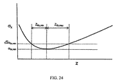
(図24に示すように)非対称である場合、ZRx,min及びZRx,maxが存在し、これらはいずれも、z0xでの最小値から、σ0x,minが√2倍増加したz値まで測定される。ZRx,minはこれら2つの値の明らかに小さい方であり、ZRx,maxは大きい方である。垂直なy軸についても同一の分析を実施できる。 When asymmetric (as shown in FIG. 24), Z Rx, min and Z Rx, max are present, all of which are z with σ 0x, min increased by √2 times from the minimum value at z 0x. Measured up to the value. Z Rx, min are clearly smaller of these two values, and Z Rx, max are larger. The same analysis can be performed on the vertical y-axis.
レーザビームの発散は、最小のレイリー範囲を有する方向において比較的短い距離にわたって発生するため、切断に使用されるパルスレーザビームの強度分布を制御することにより、ZRx及びZRyの最小値を可能な限り大きくすることができる。ZRxの最小値ZRx,min及びZRyの最小値ZRy,minは、非軸対称ビームに関しては異なるため、損傷領域の形成時にZRx,min及びZRy,minのうちの小さい方を可能な限り大きくする強度分布を有するレーザビームを使用してよい。 Since the divergence of the laser beam occurs over a relatively short distance in the direction with the minimum Rayleigh range, the minimum values of Z Rx and Z Ry are possible by controlling the intensity distribution of the pulsed laser beam used for cutting. It can be as large as possible. Z Rx minimum value Z Rx, min and Z Ry minimum value Z Ry of, min is different because for non-axisymmetric beam, Z Rx during the formation of the damaged region, min and Z Ry, the smaller of the min A laser beam with an intensity distribution that is as large as possible may be used.
異なる実施形態では、ZRx,min及びZRy,minのうちの小さい方は、50μm以上、100μm以上、200μm以上、300μm以上、500μm以上、1mm以上、2mm以上、3mm以上、5mm以上、50μm〜10mm、100μm〜5mm、200μm〜4mm、300μm〜2mm等である。 In different embodiments, the smaller of Z Rx, min and Z Ry, min is 50 μm or more, 100 μm or more, 200 μm or more, 300 μm or more, 500 μm or more, 1 mm or more, 2 mm or more, 3 mm or more, 5 mm or more, 50 μm to It is 10 mm, 100 μm to 5 mm, 200 μm to 4 mm, 300 μm to 2 mm, and the like.
本明細書で明記したZRx,min及びZRy,minのうちの小さい方の値及び範囲は、等式(27)で定義されたスポットサイズパラメータw0,minの調整によって、上記被加工物がそれに対して透明となるような様々な波長に関して達成できる。異なる実施形態では、スポットサイズパラメータw0,minは、0.25μm以上、0.50μm以上、0.75μm以上、1.0μm以上、2.0μm以上、3.0μm以上、5.0μm以上、0.25μm〜10μm、0.25μm〜5.0μm、0.25μm〜2.5μm、0.50μm〜10μm、0.50μm〜5.0μm、0.50μm〜2.5μm、0.75μm〜10μm、0.75μm〜5.0μm、0.75μm〜2.5μm等である。 The smaller value and range of Z Rx, min and Z Ry, min specified in the present specification are the above-mentioned workpieces by adjusting the spot size parameter w 0, min defined by the equation (27). Can be achieved for various wavelengths such that is transparent to it. In different embodiments, the spot size parameters w 0, min are 0.25 μm and above, 0.50 μm and above, 0.75 μm and above, 1.0 μm and above, 2.0 μm and above, 3.0 μm and above, 5.0 μm and above, 0. .25 μm to 10 μm, 0.25 μm to 5.0 μm, 0.25 μm to 2.5 μm, 0.50 μm to 10 μm, 0.50 μm to 5.0 μm, 0.50 μm to 2.5 μm, 0.75 μm to 10 μm, 0 It is .75 μm to 5.0 μm, 0.75 μm to 2.5 μm, and the like.
損傷領域の形成に使用されるレーザビームのレイリー範囲は、同一波長を有するガウスビームのレイリー範囲より大きくなり得る。従って、共通の波長λにおける、(等式(22)又は(23)において明記されているような)ガウスビームのレイリー範囲ZRに対するZRx,min及びZRy,minのうちの小さい方の比は、2以上、5以上、10以上、25以上、50以上、100以上、250以上、500以上、1000以上、2〜1500、5〜1250、10〜1000、25〜1000、100〜1000等であってよい。 The Rayleigh range of the laser beam used to form the damaged area can be larger than the Rayleigh range of a Gaussian beam having the same wavelength. Therefore, the smaller ratio of Z Rx, min and Z Ry, min to the Rayleigh range Z R of the Gaussian beam (as specified in equation (22) or (23)) at the common wavelength λ. 2 or more, 5 or more, 10 or more, 25 or more, 50 or more, 100 or more, 250 or more, 500 or more, 1000 or more, 2 to 1500, 5 to 1250, 10 to 1000, 25 to 1000, 100 to 1000, etc. It may be there.
非回折又は準非回折ビームは一般に、半径に対して非単調減少するもの等の、複雑な強度プロファイルを有する。ガウスビームと同様に、有効スポットサイズWo,effは、非軸対称ビームに関して、最大強度の径方向位置(r=0)からの、強度が最大強度の1/e2まで低下するいずれの方向における最短径方向距離として定義できる。有効スポットサイズWo,effに基づくレイリー範囲に関する基準は、損傷領域の形成のための非回折又は準非回折ビームに関して: Non-diffraction or quasi-non-diffraction beams generally have complex intensity profiles, such as those that diminish non-monotonically with respect to radius. Like the Gaussian beam, the effective spot sizes Wo and eff are in any direction from the radial position of the maximum intensity (r = 0) with respect to the non-axisymmetric beam where the intensity decreases to 1 / e 2 of the maximum intensity. Can be defined as the shortest radial distance in. Criteria for Rayleigh range based on effective spot size Wo, eff are for non-diffraction or quasi-non-diffraction beams for the formation of damaged areas:
のように具体化でき、ここでFDは、少なくとも10、少なくとも50、少なくとも100、少なくとも250、少なくとも500、少なくとも1000、10〜2000、50〜1500、100〜1000の値を有する無次元発散係数である。等式(31)を等式(22)又は(23)と比較することにより、非回折又は準非回折ビームに関して、有効ビームサイズが2倍になる距離、即ち式(31)中の「ZRx,min、ZRy,minのうちの小さい方」が、仮に典型的なガウスビームを使用する場合に予想される距離のFD倍となることを確認できる。 It is embodied as, where F D is at least 10, at least 50, at least 100, at least 250, at least 500, dimensionless divergence coefficient having a value of at least 1000,10~2000,50~1500,100~1000 Is. By comparing equation (31) with equation (22) or (23), the effective beam size is doubled for non-diffraction or quasi-non-diffraction beams, i.e. "Z Rx" in equation (31). , Min , Z Ry, and min , whichever is smaller, can be confirmed to be FD times the expected distance when a typical Gaussian beam is used.
上述のように、レイリー範囲は、ビームのピーク強度が1/2倍に下降する距離を測定することによっても決定できる。本明細書ではこれを、レイリー範囲を決定するための強度法と呼ぶ。 As mentioned above, the Rayleigh range can also be determined by measuring the distance at which the peak intensity of the beam drops by a factor of two. This is referred to herein as the intensity method for determining the Rayleigh range.
本発明者らは、有効スポットサイズWo,effに基づくレイリー範囲に関する基準を、損傷領域の形成のための非回折又は準非回折ビームに関して: We set the criteria for Rayleigh range based on effective spot size Wo, eff with respect to non-diffraction or quasi-non-diffraction beams for the formation of damaged areas:
のように具体化することもできることを発見した。 I found that it can also be embodied like this.
レイリー範囲を決定する際、分散法、即ち等式(31)若しくは(31’)を利用する方法を用いることができ、又は強度法を用いることができる。強度法を用いる場合、xとyとの間に差がないため、1つの解答、即ち最小レイリー範囲に関して1つの値しか存在しない。 In determining the Rayleigh range, the dispersion method, i.e. the method utilizing equations (31) or (31'), can be used, or the intensity method can be used. When using the intensity method, there is no difference between x and y, so there is only one value for one solution, the minimum Rayleigh range.
無次元発散係数FDは、レーザビームが準非回折性であるかどうかを決定するための基準を提供する。本明細書中で使用される場合、「レーザビーム(laser beam)」は、該レーザビームが、FDの値≧10において式(31)を満たす場合に、準非回折性とみなされる。FDの値が増加するに従って、レーザビームは、非回折状態に更に完璧に近づく。 Dimensionless divergence factor F D provides a reference for the laser beam to determine whether a quasi-diffractive. As used herein, "laser beam (laser beam)" means that the laser beam, when satisfying the formula (31) at a value ≧ 10 of F D, is regarded as quasi-diffractive. According to the value of F D increases, the laser beam is further approaches perfect undiffracted state.
ここで図3〜7Aを参照すると、準非回折性のパルスレーザビーム112を生成する(図3〜7A)、及びいくつかの実施形態では透明被加工物160において非軸対称ビームスポット114を生成する(図4〜7A)、光学アセンブリ100が図示されている。例えば図3は、例えば準非回折性のパルスレーザビーム112を生成するための、パルスレーザ加工用の従来の光学アセンブリ100が示されている。更に図4〜7Aはそれぞれ、図3に示されていない追加の構成要素及び構成を備える、透明被加工物160において非軸対称ビームスポット114を形成するための光学アセンブリ100を示す。例えば図4の光学アセンブリ100は、ビーム経路111に対してオフセットされた非球面光学素子120を備え、図5A及び5Bの光学アセンブリ100は、ビーム経路111内に位置決めされた1つ以上の光学遮断素子140を含む。更に、図6及び7Aの光学アセンブリ100はそれぞれ、パルスレーザビーム112の第1のビーム部分をパルスレーザビーム112の第2のビーム部分からデコヒーレント化する要構成された、1つ以上のデコヒーレント化用光学素子を備える。特に、図6の光学アセンブリ100のデコヒーレント化用光学素子は、ビーム経路111内に位置決めされた光遅延プレート142を備え、図7Aの光学アセンブリ100のデコヒーレント化用光学素子は、ビーム経路111内に位置決めされた(図7Bにも図示されている)分割1/4波長板150を備える。本明細書中で使用される場合、「デコヒーレント化する(decohere)」は、パルスレーザビームの第1の部分を、パルスレーザビームの第2の部分と非コヒーレント状態とすることを意味する。
Referring here to FIGS. 3-7A, a quasi-non-diffractive
図3〜7Aはそれぞれ、ビーム源110、非球面光学素子120(例えばアキシコンレンズ)、第1のレンズ130、及び第2のレンズ132を備える。更に、透明被加工物160は、ビーム源110が出力したパルスレーザビーム112が例えば非球面光学素子120と、それに続いて第1のレンズ130及び第2のレンズ132とを横断した後で、透明被加工物160に照射されるように、位置決めしてよい。光軸102はビーム源110と透明被加工物160との間に、Z軸に沿って延在する。更に、図3〜7Aの光学アセンブリ100は任意に、ビーム経路111内において非球面光学素子120と透明被加工物160との間に位置決めされた、ドーブプリズム180を備えてよい。ドーブプリズム180は図5A、5B及び6に示されているが、本明細書に記載のいずれの光学アセンブリ100がドーブプリズム180を備えてよいことを理解されたい。更に、光軸102の周りでのドーブプリズム180の回転は、パルスレーザビーム112のビーム断面(例えば非軸対称ビームスポット114)を回転させることができる。非軸対称ビームスポット114の回転により、非軸対称ビームスポット114の長軸116の、透明被加工物160の所望の分割線165に沿った配向が促進される。以下の実施形態において説明されるように、非軸対称ビームスポット114を回転させる他の方法も考えられる。
FIGS. 3 to 7A include a
ここでもまた図3〜7Aを参照すると、ビーム源110は、パルスレーザビーム112を出力するよう構成された、いずれの公知の又はまだ開発されていないビーム源110を備えてよい。動作時、輪郭線170の欠陥172が、透明被加工物160と、ビーム源110が出力したパルスレーザビーム112との相互作用によって製造される。いくつかの実施形態では、ビーム源110は、例えば1064nm、1030nm、532nm、530nm、355nm、343nm、又は266nm、又は215nmの波長を備えるパルスレーザビーム112を出力してよい。更に、透明被加工物160内に欠陥172を形成するために使用されるパルスレーザビーム112は、選択されたパルスレーザ波長に対して透明である材料に対して十分に好適となり得る。
Again, referring to FIGS. 3-7A, the
欠陥172の形成に好適なレーザ波長は、透明被加工物160による吸収及び散乱を合わせた損失が十分に小さい波長である。実施形態では、該波長における、透明被加工物160による吸収及び散乱を合わせた損失は、20%/mm未満、又は15%/mm未満、又は10%/mm未満、又は5%/mm未満、又は1%/mm未満であり、ここで寸法「/mm」は、パルスレーザビーム112の伝播の方向(例えばZ方向)における透明被加工物160内の距離1ミリメートルあたりを意味する。多くのガラス被加工物に関する代表的な波長としては、Nd3+(例えば1064nm付近の基本波長並びに532nm、355nm及び266nm付近の高次高調波長を有するNd3+:YAG又はNd3+:YVO4)の基本波長及び高調波長が挙げられる。所与の基板材料に関して吸収及び散乱を合わせた損失の要件を満たす、スペクトルの紫外部分、可視部分及び赤外部分の他の波長も、使用できる。
The laser wavelength suitable for forming the
動作時、ビーム源110が出力したパルスレーザビーム112は、透明被加工物160内に多光子吸収(multi‐photon absorption:MPA)を生成できる。MPAは、分子をある状態(通常はグランド状態)からより高いエネルギの電子的状態(即ちイオン化)に励起する、同一の又は異なる周波数の2つ以上の光子の同時吸収である。これに関与する分子の低エネルギ状態と高エネルギ状態との間のエネルギの差は、関与する光子のエネルギの合計に等しい。誘起吸収とも呼ばれるMPAは、2次又は3次(又はより高次)プロセスであってよく、これは例えば、線形吸収よりも数桁弱い。これは、2次誘起吸収の強度が光強度の2乗に比例し得、従って非線形光学プロセスであるという点で、線形吸収とは異なる。
During operation, the
輪郭線170を形成する穿孔ステップは、ビーム源110(例えば超短パルスレーザ)を、図3〜7Aに図示され以下で説明される光学系と組み合わせて利用して、透明被加工物160上に非軸対称ビームスポット114を投射し、図1Bのパルスレーザビーム焦線113を生成できる。パルスレーザビーム焦線113は、上で定義したような非軸対称ガウス‐ベッセルビーム等の準非回折ビームを含み、これにより、透明被加工物160を完全に穿孔して、透明被加工物160内に一連の欠陥172を形成する。いくつかの実施形態では、個々のパルスのパルス持続時間は、約1ピコ秒〜約100ピコ秒、例えば約5ピコ秒〜約20ピコ秒であり、また個々のパルスの繰り返し数は、約1kHz〜4MHz、例えば約10kHz〜約3MHz、又は約10kHz〜約650kHzであってよい。
The drilling step of forming the
図7C〜7Dも参照すると、上述の個々のパルス繰り返し数における単一パルスの動作に加えて、パルスを、2つのパルス500A(例えばサブパルス)以上(例えば1回のパルスバーストあたり、3パルス、4パルス、5パルス、10パルス、15パルス、20パルス、又はより多数のパルス、例えば1回のパルスバースト500あたり1〜30パルス、又は1回のパルスバースト500あたり5〜20パルス)のパルスバースト500で生成してよい。パルスバースト500内のパルス500Aは、約1nsec〜約50nsec、例えば約10nsec〜約30nsec、例えば約20nsecの持続時間によって隔てられていてよい。他の実施形態では、パルスバースト500内のパルス500Aは、最高100psec(例えば、0.1psec、5psec、10psec、15psec、18psec、20psec、22psec、25psec、30psec、50psec、75psec、又はこれらの間のいずれの範囲)の持続時間によって隔てられていてよい。所与のレーザに関して、パルスバースト500内の隣接するパルス500Aの間の時間間隔Tp(図7D)は、比較的均一(例えば互いの約10%以内)であってよい。例えばいくつかの実施形態では、パルスバースト500内の各パルス500Aは、後続のパルスからおよそ20nsec(50MHz)だけ時間的に隔てられている。例えば各パルスバースト500間の時間は、約0.25マイクロ秒〜約1000マイクロ秒、例えば約1マイクロ秒〜約10マイクロ秒、又は約3マイクロ秒〜約8マイクロ秒であってよい。
Also with reference to FIGS. 7C-7D, in addition to the single pulse operation at the individual pulse repetitions described above, the pulses are two
本明細書に記載のビーム源110の例示的な実施形態のうちのいくつかでは、時間間隔Tb(図7D)は、バースト繰り返し数が約200kHzであるパルスレーザビーム112を出力するビーム源110に関して、約5マイクロ秒である。レーザバースト繰り返し数は、あるバースト内の最初のパルスから、次のバースト内の最初のパルスまでの時間Tbに関連する(レーザバースト繰り返し数=1/Tb)。いくつかの実施形態では、レーザバースト繰り返し数は約1kHz〜約4MHzであってよい。実施形態では、レーザバースト繰り返し数は例えば約10kHz〜650kHzであってよい。各バースト内の最初のパルスから、次のバースト内の最初のパルスまでの時間Tbは、約0.25マイクロ秒(4MHzのバースト繰り返し数)〜約1000マイクロ秒(1kHzのバースト繰り返し数)、例えば約0.5マイクロ秒(2MHzのバースト繰り返し数)〜約40マイクロ秒(25kHzのバースト繰り返し数)、又は約2マイクロ秒(500kHzのバースト繰り返し数)〜約20マイクロ秒(50kHzのバースト繰り返し数)であってよい。正確なタイミング、パルス持続時間、及びバースト繰り返し数は、レーザの設計に応じて変動し得るが、高強度の短パルス(Td<20psec、及びいくつかの実施形態では、Td≦15psec)が特に良好に動作することが分かっている。
In some of the exemplary embodiments of the
バースト繰り返し数は、約1kHz〜約2MHz、例えば約1kHz〜約200kHzであってよい。バースト形成又はパルスバースト500の生成は、パルス500Aの放出が均一かつ安定した流れにならず、パルスバースト500の密集したクラスタとなるような、レーザ動作の1タイプである。パルスバーストレーザビームは、透明被加工物160の材料に基づいて、透明被加工物160の材料が該波長において略透明となるように動作するよう選択された、波長を有してよい。材料において測定されるバーストあたりの平均レーザ出力は、材料の厚さ1mmあたり少なくとも約40μJであってよい。例えば実施形態では、バーストあたりの平均レーザ出力は、約40μJ/mm〜約2500μJ/mm、又は約500μJ/mm〜約2250μJ/mmであってよい。ある具体例では、厚さ0.5mm〜0.7mmのCorning EAGLE XG透明被加工物に関して、約300μJ〜約600μJのパルスバーストが被加工物を切断及び/又は分割でき、これは約428μJ/mm〜約1200μJ/mm(即ち0.7mmのEAGLE XGガラスに関して300μJ/0.7mm、及び0.5mmのEAGLE XGガラスに関して600μJ/0.5mm)という例示的な範囲に対応する。
The number of burst repetitions may be from about 1 kHz to about 2 MHz, for example from about 1 kHz to about 200 kHz. Burst formation or pulse burst 500 generation is a type of laser operation in which the emission of the
透明被加工物160の修正に必要なエネルギは、バーストエネルギ(即ちあるパルスバースト500内に内包されたエネルギ(ここで各パルスバースト500は一連のパルス500Aを内包する))に関して、又は単一のレーザパルス(これが多数集まって1つのバーストを構成できる)内に内包されるエネルギに関して、記述できる。パルスバーストあたりのエネルギは、約25μJ〜約750μJ、例えば約50μJ〜約500μJ、又は約50μJ〜約250μJであってよい。いくつかのガラス組成物に関して、パルスバーストあたりのエネルギは約100μJ〜約250μJであってよい。しかしながら、ディスプレイ又はTFT用ガラス組成物に関して、パルスバーストあたりのエネルギはより高くなり得る(例えば、透明被加工物160の具体的なガラス組成に応じて、約300μJ〜約500μJ、又は約400μJ〜約600μJ)。このようなバーストを生成できるパルスレーザビーム112の使用は、例えばガラスである透明材料の切断又は修正に有利である。単一パルスレーザの繰り返し数によって時間的に隔てられた単一パルスの使用とは対照的に、バースト内の複数のパルスの迅速なシーケンスにわたってレーザエネルギを拡散するバーストシーケンスの使用により、材料との高強度の相互作用のタイムスケールを、単一パルスレーザによって可能なものよりも大きくすることができる。
The energy required to modify the
再び図3〜7Aを参照すると、非球面光学素子120は、ビーム源110と透明被加工物160との間において、ビーム経路111内に位置決めされる。動作時、パルスレーザビーム112、例えば入射してくるガウスビームを、非球面光学素子120を通して伝播させることにより、非球面光学素子120を越えて伝播するパルスレーザビーム112の部分が上述のように準非回折性となるように、パルスレーザビーム112を変化させることができる。非球面光学素子120は、非球面形状を備えるいずれの光学素子を含んでよい。いくつかの実施形態では、非球面光学素子120は、アキシコンレンズ、例えば負屈折アキシコンレンズ、正屈折アキシコンレンズ、反射アキシコンレンズ、回折アキシコンレンズ、プログラマブル空間光変調器アキシコンレンズ(例えば位相アキシコン)等の、円錐波面生成光学素子を含んでよい。
Referring again to FIGS. 3-7A, the aspherical
いくつかの実施形態では、非球面光学素子120は少なくとも1つの非球面表面を備え、その形状は数学的に:z’=(cr2/1)+(1−(1+k)(c2r2))1/2+(a1r+a2r2+a3r3+a4r4+a5r5+a6r6+a7r7+a8r8+a9r9+a10r10+a11r11+a12r12のように記述され、ここでz’は上記非球面表面の表面サグであり、rは、径方向における(例えばx方向又はy方向における)、上記非球面表面と光軸102の距離であり、cは上記非球面表面の表面曲率(即ちci=1/Ri(ここでRは上記非球面表面の表面半径である))であり、kは円錐定数であり、係数aiは、上記非球面表面を記述する1次〜12次非球面係数又はより高次の非球面係数(多項式非球面)である。例示的な一実施形態では、非球面光学素子120の少なくとも1つの非球面表面は、それぞれ:−0.085274788;0.065748845;0.077574995;−0.054148636;0.022077021;−0.0054987472;0.0006682955である係数a1〜a7を含み、また非球面係数a8〜a12は0である。この実施形態では、少なくとも1つの非球面表面は、円錐定数k=0を有する。しかしながら、a1の係数は非ゼロ値を有するため、これは非ゼロ値の円錐定数kを有することと同等である。従って、非ゼロの円錐定数k、非ゼロの係数a1、又は非ゼロのkと非ゼロの係数a1との組み合わせを指定することによって、同等の表面を記述できる。更にいくつかの実施形態では、少なくとも1つの非球面表面は、非ゼロ値を有する少なくとも1つの高次非球面係数a2〜a12(即ちa2、a3、…a12のうちの少なくとも1つ≠0)によって記述又は定義される。例示的な一実施形態では、非球面光学素子120は、立方体状の光学素子等の3次非球面光学素子を含み、これは非ゼロの係数a2を備える。
In some embodiments, aspheric
いくつかの実施形態では、上記非球面光学素子がアキシコンからなる場合、上記アキシコンは、約1.2°、例えば約0.5°〜約5°、又は約1°〜約1.5°、又は約0.5°〜約20°でさえある角度を有するレーザ出力表面126(例えば円錐表面)を備え、上記角度は、パルスレーザビーム112がアキシコンレンズに入るレーザ入力表面124(例えば平坦表面)に対して測定される。更に、レーザ出力表面126は、円錐の頂点で終端する。更に、非球面光学素子120は、レーザ入力表面124からレーザ出力表面126まで延在して円錐の頂点で終端する、中心線軸122を含む。他の実施形態では、非球面光学素子120はワキシコン、空間光変調器等の空間位相変調器、又は光回折格子からなってよい。動作時、非球面光学素子120は、入射するパルスレーザビーム112(例えば入射するガウスビーム)を準非回折ビームに成形し、続いてこれは、第1のレンズ130及び第2のレンズ132を通るように向けられる。
In some embodiments, when the aspherical optical element consists of an axicon, the axicon is about 1.2 °, for example about 0.5 ° to about 5 °, or about 1 ° to about 1.5 °. Alternatively, the laser output surface 126 (eg, a conical surface) having an angle of about 0.5 ° to even about 20 ° is provided, and the above angle is the laser input surface 124 (eg, a flat surface) into which the
ここでもまた図3〜7Aを参照すると、第1のレンズ130及び第2のレンズ132は、第1のレンズ130と第2のレンズ132との間のコリメート空間134内において、パルスレーザビーム112をコリメートしてよい。更に第2のレンズ132はパルスレーザビーム112を透明被加工物160内へと集束させてよく、これは撮像平面104に位置決めしてよい。いくつかの実施形態では、第1のレンズ130及び第2のレンズ132はそれぞれ平凸レンズからなる。第1のレンズ130及び第2のレンズ132がそれぞれ平凸レンズからなる場合、第1のレンズ130及び第2のレンズ132の曲率はそれぞれ、コリメート空間134に向かって配向してよい。他の実施形態では、第1のレンズ130は他のコリメートレンズからなってよく、また第2のレンズ132は、メニスカスレンズ、非球面レンズ、又は別の高次補正集束レンズからなってよい。
Again, referring to FIGS. 3-7A, the
更に、第1のレンズ130は第1の焦点距離F1を備え、第2のレンズ132は第2の焦点距離F2を備える。本明細書中で使用される場合、「焦点距離(focal length)」は、レンズとレンズの焦点との間の距離として定義される。いくつかの実施形態では、第1の焦点距離F1及び第2の焦点距離F2は等しくてよい。他の実施形態では、第1の焦点距離F1及び第2の焦点距離F2は異なっていてよく、例えば第2の焦点距離F2は第1の焦点距離F1未満であってよく、あるいは第1の焦点距離F1より大きくてよい。いくつかの実施形態では、第1のレンズ130及び第2のレンズ132は、それぞれ約10mm〜約200mm(例えば約25mm〜約200mm、又は約50mm〜150mm、又は約75mm〜約100mm、又は約25mm〜約50mm等)の焦点距離F1、F2を有してよい。
Furthermore, the
いくつかの実施形態では、第1のレンズ130は第2のレンズ132から、第1の焦点距離F1及び第2の焦点距離F2の合計だけ離間していてよく、これにより、第1のレンズ130と第2のレンズ132との間のコリメート空間134に共通の焦点面105が位置決めされる。しかしながら、他の空間的構成も考えられることを理解されたい。共通の焦点面105は、第1のレンズ130と第2のレンズ132との間のビーム経路111に沿った、第1のレンズ130から下流に第1の焦点距離F1だけ離間し、かつ第2のレンズ132から上流に第2の焦点距離F2だけ離間した場所である。本明細書中で使用される場合、「上流(upstream)」及び「下流(downstream)」は、ビーム源110に対する、ビーム経路111に沿った2つの場所又は構成部品の相対位置を指す。例えば、パルスレーザビーム112が、第2の構成部品を横断する前に第1の構成部品を横断する場合、第1の構成部品は第2の構成部品から上流にある。更に、パルスレーザビーム112が、第1の構成部品を横断する前に第2の構成部品を横断する場合、第1の構成部品は第2の構成部品から下流にある。
In some embodiments, the
ここで図4を参照すると、径方向(例えばビーム伝播方向に対して垂直な、パルスレーザビーム112の半径に沿った方向)において、パルスレーザビーム112のビーム経路111に対してオフセットして位置決めされた、非球面光学素子120を備える、光学アセンブリ100の実施形態が図示されている。非球面光学素子120をビーム経路111に対してオフセットさせることにより、透明被加工物160上に投射される、結果として得られるビームスポットは、図2に示す非軸対称ビームスポット114からなるものとすることができる。非球面光学素子120は、オフセット距離aだけ、ビーム経路111からオフセットして(例えばX‐Y平面内でオフセットして)位置決めしてよい。特に、オフセット距離aは、パルスレーザビームを非球面光学素子120のレーザ入力表面124に照射したときの、非球面光学素子120の中心線軸122と、パルスレーザビームの断面中心との間の、X‐Y平面内での距離である。非球面光学素子120と上記ビーム経路との間の相対的なオフセットは、非球面光学素子120をX‐Y平面に沿って変位させること、ビーム源110をX‐Y平面に沿って変位させること、又はこれら両方によって達成できる。結果として得られるビームスポットの対称性を十分に破壊するために必要なオフセットの大きさは、パルスレーザビーム112の直径に左右され、入力されるレーザビームの直径が小さいほど、対称性を十分に破壊するために必要なオフセットは小さくなる。いくつかの実施形態では、オフセット距離aは、約10マイクロメートル〜約500マイクロメートル、例えば、20マイクロメートル、50マイクロメートル、100マイクロメートル、250マイクロメートル等であってよい。いくつかの実施形態では、オフセット距離aは、約20マイクロメートル〜約100マイクロメートル、又は約50マイクロメートル〜約100マイクロメートル等であってよい。いくつかの実施形態では、上記オフセット距離は、パルスレーザビーム112と非球面光学素子120との間の接触位置における(例えば非球面光学素子120のレーザ入力表面124における)パルスレーザビーム112の断面直径の約10%〜約75%の距離であってよい。
Here, referring to FIG. 4, in the radial direction (for example, a direction perpendicular to the beam propagation direction and along the radius of the pulsed laser beam 112), the
非球面光学素子120をビーム経路111に対してオフセットさせることにより、結果として得られるパルスレーザビーム112は、全体としての強度が、例えば約4倍低下し得る。更に、パルスレーザビーム112の断面は、X‐Y平面内でX方向、Y方向、又はこれらの組み合わせにおいて、約1.2〜約2倍、例えば1.4倍、1.6倍、1.8倍等だけ広がり得る。パルスレーザビーム112の断面を広げることにより、この広がりの方向に長軸116を有する非軸対称ビームスポット114が形成される。結果として得られるパルスレーザビーム112は、光線の非軸対称円錐を含んでよく、これは、第1のレンズ130を横断した後、コリメート空間134内に非軸対称リングを形成する。更に、パルスレーザビーム112の断面(例えば非軸対称ビームスポット114)は、非球面光学素子120を光軸102の周りで回転させることによって、回転させることができる。
By offsetting the aspherical
ここで図5A及び5Bを参照すると、ビーム源110と透明被加工物160との間で伝播するパルスレーザビーム112の一部分を遮断する、ビーム経路111に沿った1つ以上の遮断位置141に位置決めされた、1つ以上の光学遮断素子140(例えば不透明光学素子)を備える、光学アセンブリ100の実施形態が図示されている。いくつかの実施形態では、光学遮断素子140は不透明プレートからなってよく、これは更にアパーチャを備えてよい。例えば光学遮断素子140は、金属プレート、又は破損若しくは損傷することなくパルスレーザビーム112に耐えることができる他の物質からなってよい。光学遮断素子140は、光学遮断素子140が、パルスレーザビーム112のビーム強度の約5%〜約95%、例えば少なくとも約10%、20%、30%、40%、50%、60%、70%、80%、85%、90%等を遮断するように、ビーム経路111内に位置決めしてよい。一例として、光学遮断素子140は、パルスレーザビーム112のビーム強度の約25%〜約80%を遮断する。パルスレーザビーム112のビーム強度の、比較的高いパーセンテージを遮断することにより、非軸対称ビームスポット114の短軸115に対する、非軸対称ビームスポット114の長軸116の長さが増大する。しかしながら、パルスレーザビーム112のビーム強度の、比較的高いパーセンテージを遮断することにより、光学遮断素子140において失われる、パルスレーザビーム112の力の量が増大する。
Here, referring to FIGS. 5A and 5B, positioning is performed at one or
いくつかの実施形態では、光学遮断素子140は、パルスレーザビーム112のある断面セクタ(即ちパルスレーザビーム112の中心位置からパルスレーザビーム112の最外直径まで延在する、パルスレーザビーム112の方位角範囲又は「パイスライス(pie slice)」によって画定される、セクタ)を遮断してよい。セクタの形態の光学遮断素子140は、パルスレーザビーム112の全半径において同一パーセンテージの光線を遮断するという利点を有する。このような光学アセンブリでは、光学系は、特定の半径の光線を、パルスレーザビーム焦線113に沿った対応する具体的な位置へとマッピングする。図5A及び5Bに示す例示的実施形態では、非球面光学素子120の近傍の低半径光線が、パルスレーザビーム焦線113の上流端部の複数の位置にマッピングされることになり、また非球面光学素子120の近傍の高半径光線が、パルスレーザビーム焦線113の下流端部の複数の位置にマッピングされることになる。光学遮断素子140が、大きな半径におけるものよりも小さな半径における光線を大きな割合で切り取る場合、パルスレーザビーム焦線113の断面(一例として非軸対称ビームスポット114)の楕円率の大きさ又はアスペクト比は、その長さ全体にわたって変化することになる。従って、光学遮断素子140をパイスライスの形状に成形することにより、パルスレーザビーム焦線113の、結果として得られる断面が、パルスレーザビーム焦線113の全長を通して一定の楕円率を維持することが保証される。
In some embodiments, the
他の実施形態では、光学遮断素子140は、パルスレーザビーム112の断面弦部分を遮断してよく、ここでパルスレーザビーム112の断面弦部分は、パルスレーザビーム112の断面の周と、パルスレーザビーム112の任意の断面弦とによって境界が画定される。更にこの例示的実施形態では、ビーム経路111内に位置決めされた光学遮断素子140の一部分は、任意の断面弦と連続している。更に、光学遮断素子140は、パルスレーザビーム112のいずれの任意の断面部分を遮断してよいことを理解されたい。
In another embodiment, the
更に光学遮断素子140は、ビーム源110と透明被加工物160との間に位置決めしてよい。光学遮断素子140がビーム源110と透明被加工物160との間に位置決めされるため、動作時、パルスレーザビーム112は、非球面光学素子120を通り、光学遮断素子140を越えて進むことになる(例えばパルスレーザビーム112の遮断されなかった部分は光学遮断素子140を超えて進むが、パルスレーザビーム112の遮断される部分は光学遮断素子140を越えて進まない)。更にパルスレーザビーム112は、ビーム伝播方向(例えばZ方向)に沿った非球面光学素子120及び光学遮断素子140の位置決めの相対的な順序にかかわらず、非球面光学素子120を通り、光学遮断素子140を越えて進むことになる。例えば光学遮断素子140を非球面光学素子120から上流に位置決めしてよく、これにより光学遮断素子140は、ビーム源110と非球面光学素子120との間に位置決めされる。更に、光学遮断素子140を非球面光学素子120から下流に位置決めしてよく、これにより光学遮断素子140は、非球面光学素子120と透明被加工物160との間に位置決めされる。
Further, the
いくつかの実施形態では、光学遮断素子140は、第1のレンズ130と第2のレンズ132との間のコリメート空間134内において、例えば共通の焦点面105に位置決めしてよい。更にパルスレーザビーム焦線113の断面(例えば非軸対称ビームスポット114)は、光学遮断素子140を光軸102の周りで回転させることによって、回転させることができる。いくつかの実施形態では、非軸対称ビームスポット114は、非球面光学素子120をビーム経路111に対してオフセットすること、及びパルスレーザビーム112の一部分を光学遮断素子140によって遮断することの両方によって形成できる。非球面光学素子120のオフセットを用いて、レーザビームエネルギのうちのより多くの部分を、光学遮断素子140を通るように向ける場合、オフセットと遮断との上記組み合わせは、楕円形又はその他の非軸対称ビームスポット114が生成されて透明被加工物160上に投射されることを依然として保証したまま、光学遮断素子140によって引き起こされる力の損失の量を低減できる。
In some embodiments, the
更に図5Bに示すように、いくつかの実施形態では、光学アセンブリ100は、第1の光学遮断素子140a及び第2の光学遮断素子140bを備えてよい。第1の光学遮断素子140aは、第1の遮断位置141aにおいてビーム経路111内に位置決めされ、上記第2の光学遮断素子は、第2の遮断位置141bにおいてビーム経路111内に位置決めされる。第1の光学遮断素子140a及び第2の光学遮断素子140bは、これらがそれぞれ、ビーム経路111の一部分、例えばビーム経路111の異なる部分を遮断するように、位置決めしてよい。いくつかの実施形態では、第1の光学遮断素子140a及び第2の光学遮断素子140bはそれぞれ、パルスレーザビーム112の異なる断面セグメントを遮断してよい。例えば光学遮断素子140a、140bは、パルスレーザビーム112の断面の対向する側を遮断するよう平行に位置決めされた、各被遮断断面セグメントの断面弦部分を画定してよい。あるいは別の例では、光学遮断素子140a、140bは、パルスレーザビーム112の断面の対向する側を遮断するよう、円の異なる複数のセクタを画定してよい。
Further, as shown in FIG. 5B, in some embodiments, the
いくつかの実施形態では、第1の遮断位置141a及び第2の遮断位置141bは、図5Bに示すように、光軸102に沿って同一のZ軸位置に位置決めされる。他の実施形態では、第1の遮断位置141a及び第2の遮断位置141bは、光軸102に沿って異なる位置であってよい。更に、第1の遮断素子140a及び第2の遮断素子140bは合わせて、パルスレーザビーム112の強度の約5%〜約75%を遮断できる。更に、第1の遮断素子140a及び第2の遮断素子140bは、パルスレーザビーム112の強度の同一のパーセンテージ、又はパルスレーザビーム112の強度の異なるパーセンテージを遮断できる。
In some embodiments, the first blocking position 141a and the second blocking position 141b are positioned at the same Z-axis position along the
更に、図5A及び5Bの遮断位置141、141a、141bはそれぞれ、ビーム源110と非球面光学素子120との間に図示されているが、遮断位置141、141a、141bは、ビーム源110と透明被加工物160との間の、例えば第1のレンズ130と第2のレンズ132との間の、例えば共通の焦点面105のいずれの位置であってよいことを理解されたい。理論によって制限されることを望むものではないが、パルスレーザビーム112を複数の(例えば2つの)光学遮断素子140で遮断することにより、複数のビームスポットを透明被加工物の撮像表面162上に投射でき、上記複数のビームスポットは、複数のビームスポットが全体として、透明被加工物160において図2に示すような非軸対称ビームスポット114を画定するように成形される。
Further, the cutoff positions 141, 141a, 141b in FIGS. 5A and 5B are shown between the
ここで図6を参照すると、ビーム源110と透明被加工物160との間に位置決めされた1つ以上の光遅延プレート142を備える、光学アセンブリ100の例示的実施形態が図示されている。動作時、光遅延プレート142をビーム経路111内に位置決めすると、パルスレーザビーム112の一部分に光減少遅延を誘発して、パルスレーザビーム112の第1の部分を上記光遅延プレートを通るように向けることで上記第1のビーム部分の位相差を誘発することによって、パルスレーザビーム112の第1のビーム部分を第2のビーム部分からデコヒーレント化することにより、図2に示す非軸対称ビームスポット114を形成できる。光遅延プレート142は、パルスレーザビーム112の約50%(例えばパルスレーザビーム112の強度の約50%)が光遅延プレート142を横断するように、ビーム経路111内に位置決めしてよい。理論によって制限されることを望むものではないが、パルスレーザビーム112の半分にわたる光遅延は、透明被加工物160における非軸対称ビームスポット114を一体として画定する2つのビームを形成できる。更に、パルスレーザビーム112の断面(例えば非軸対称ビームスポット114)は、光遅延プレート142を光軸102の周りで回転させることによって、回転させることができる。更に、光遅延プレート142は、非球面光学素子120の上流又は下流に位置決めしてよい。例えばいくつかの実施形態では、光遅延プレート142は非球面光学素子120と透明被加工物160との間に位置決めされ、他の実施形態では、光遅延プレート142はビーム源110と非球面光学素子120との間に位置決めされる。
Here, with reference to FIG. 6, an exemplary embodiment of an
パルスレーザビーム112の一部分(例えば1/2)を光遅延させることにより、上記ビームの、光遅延プレート142を横断する部分と、上記ビームの、光遅延プレート142を横断しない部分とが、非コヒーレント状態で組み合わされる場合、単一の非軸対称ビームスポット114を形成できる。非コヒーレント状態を達成するために、パルスレーザビーム112のコヒーレンス長は、光遅延プレート142の光学的厚さより短くしてよい。このような場合、2つのビームの光遅延は、いずれの正確な量に設定する又は精密に制御する必要がなく、上記光遅延はレーザパルスのコヒーレンス時間より大きいだけでよい。これは、レーザビームのこれら2つの部分の間の光位相差をランダム化することと略同等である。ある個別のレーザパルスのコヒーレンス時間TCは、当該技術分野で公知の方法を用いて計算でき、数学的にはTC=λ2/cΔλとして記述され、ここでλは放射の波長であり、Cは光の速度であり、Δλは該レーザパルスのスペクトル帯域幅である。光遅延プレート142によって供給される厚さの差は、レーザパルスのコヒーレンス時間より大きくてよく、又はこれと同等のものとして、プレート内のレーザパルスのコヒーレンス長より大きくてよく、上記コヒーレンス長は、数学的に:
として記述され、ここでnは光遅延プレート142の材料の屈折率である。例えばスペクトルパルス幅が12.2nmの1030nmレーザに関して、コヒーレンス時間TCは約290psecとなり、ビームをデコヒーレント化するために必要なn=1.5のガラスプレートの厚さは、38マイクロメートル超となる。別の例では、スペクトルパルス幅が0.38nmの1064nmレーザに関して、コヒーレンス時間は約290psecとなり、ビームをデコヒーレント化するために必要なn=1.5のガラスプレートの厚さは、1.3mm超となる。
Where n is the index of refraction of the material of the
理論によって制限されることを望むものではないが、正確なコヒーレンス時間及びコヒーレンス長は、レーザパルスの正確な時間的及び空間的形状に左右され、従って上述の式は近似値である。よって、上述の式によって計算された値よりわずかに小さくてよい(例えば約10%小さい、約25%小さい、約50%小さい等)厚さで、遅延プレートの十分なデコヒーレント化機能を達成できる。 Although not desired to be limited by theory, the exact coherence time and coherence length depend on the exact temporal and spatial shape of the laser pulse, so the above equation is an approximation. Thus, a sufficient decoherent function of the delay plate can be achieved with a thickness that may be slightly smaller than the value calculated by the above equation (eg, about 10% smaller, about 25% smaller, about 50% smaller, etc.). ..
更にいくつかの実施形態では、ビームの2つの部分をデコヒーレント化するのではなく、光遅延プレート142を、特定の光遅延を誘発するように構成してよく、例えば光遅延プレート142は、パルスレーザビーム112の半分にわたってπの位相差(ここでレーザ波長の1つの光周期は2πラジアンの光位相をカバーすると考えられるため、πである位相差は光周期の1/2の遅延である)、パルスレーザビーム112の半分にわたって0.875πの位相差、及びいくつかの実施形態では、レーザビームの半分にわたって0.5πの位相差を誘発してよい。単にビームの2つの部分の間の正確な光位相遅延を調整することによって、ビームの強度断面の正確なプロファイルを、ビームの中心付近の2つの等しい高強度スポットというものから、ビームの中心付近の一方のスポットがより高い強度を有し、かつもう一方がより低い強度を有するというものへ、そして他の更に複雑な干渉パターンへと変化させることができる。光遅延プレート142が誘発する特定の光位相差は、光遅延プレート142の光学的厚さと相関する。しかしながら、このような系が非軸対称ビームスポット114を生成するものの、得られるビームスポットは、2つのビーム部分の正確な光経路長に影響されやすく、これは温度及び湿度といった環境変化によって変化し得る。更にこのようなマルチスポットパターンは、複雑な多軸応力集中を有し、これは、割れの形成の制御のために、楕円形コアを有するビームほど有用な応力集中ではない場合がある。
In some further embodiments, the
ここで図7A及び7Bを参照すると、ビーム源110と透明被加工物160との間に位置決めされた分割1/4波長板150を備える、光学アセンブリ100の実施形態が図示されている。分割1/4波長板150は、第1の速軸156a及び第1の遅軸158aを有する第1のプレート部分152を備える。分割1/4波長板150はまた、第2の速軸156b及び第2の遅軸158bを有する第2のプレート部分154を備える。更に、第1の速軸156aは第2の速軸156bに対して垂直であり、第1の遅軸158aは第2の遅軸158bに対して垂直である。パルスレーザビーム112が分割1/4波長板150を横断すると、第1の速軸156a及び第1の遅軸158aを有する第1のプレート部分152は、パルスレーザビーム112の第1のビーム部分を第1の偏光(例えば特定の水平、垂直又は円偏光)に偏光させ、第2の速軸156bを有する第2のプレート部分154は、パルスレーザビーム112の第2のビーム部分を第2の偏光(例えば別の特定の水平、垂直又は円偏光)に偏光させる。第1のビーム部分を第1の偏光に偏光させ、第2のビーム部分を、第2のビーム部分に対して垂直な第2の偏光に偏光させることにより、第1のビーム部分を第2のビーム部分からデコヒーレント化する。
Here, with reference to FIGS. 7A and 7B, an embodiment of an
更に、第1の偏光を第2の偏光に対して垂直とすることにより、第1のビーム部分及び第2のビーム部分は分割1/4波長板150から下流において非コヒーレント状態で組み合わされて、図2に示す非軸対称ビームスポット114を形成する。理論によって制限されることを望むものではないが、直交する偏光(例えば垂直と水平、右回りの円と左回りの円)を有する2つのパルスレーザビーム部分は干渉せず、それぞれが透明被加工物160上に投射された場合、各ビーム部分は非コヒーレント状態で組み合わされて、合わせて非軸対称ビームスポット114(例えば楕円形)を形成する。ある説明的な例として、第1の偏光及び第2の偏光はそれぞれ、約90°離間して位置決めされたポアンカレ球上の位置を構成し、従ってこれらは直交する。第1のビーム部分と第2のビーム部分との間の非コヒーレント状態の組み合わせは、いずれの2つの直交する偏光で起こり得ることを理解されたい。
Further, by making the first polarized light perpendicular to the second polarized light, the first beam portion and the second beam portion are combined in a non-coherent state downstream from the
図7Aに示すように、光学アセンブリ100は、偏光子144及び1/4波長板146を更に備えてよい。偏光子144及び1/4波長板146はそれぞれ、ビーム経路111内においてビーム源110と分割1/4波長板150との間に位置決めされ、従ってパルスレーザビーム112は、分割1/4波長板150を横断する前に偏光子144及び1/4波長板146を横断する。動作時、偏光子144は、1つ以上の特定の変更を、偏光子144の横断からフィルタリング(例えば横断を防止)できる。1/4波長板146は、パルスレーザビーム112を単一の偏光へと偏光させることができ、これによりパルスレーザビーム112は、パルスレーザビーム112が分割1/4波長板150に到達するとき、右回り円偏光又は左回り円偏光といった単一の偏光を含む。更に図7Aに示すように、分割1/4波長板150はビーム経路111内において、1/4波長板146と透明被加工物160との間に位置決めされる。分割1/4波長板150は、非球面光学素子120の上流又は下流に位置決めしてよい。例えばいくつかの実施形態では、分割1/4波長板150は、非球面光学素子120と透明被加工物160との間に位置決めされ、また他の実施形態では、分割1/4波長板150はビーム源110と非球面光学素子120との間に位置決めされる。
As shown in FIG. 7A, the
図7Aに示す比限定的な例では、分割1/4波長板150を、第1のレンズ130と第2のレンズ132との間のコリメート空間134内に位置決めしてよく、例えば共通の焦点面105に位置決めしてよく、これにより、分割1/4波長板150の第1のプレート部分152と第2のプレート部分154との間の接触位置での相互作用による、パルスレーザビーム112の力の損失の量が最小となる。
In the limited ratio example shown in FIG. 7A, the
分割1/4波長板150を、2つのプレート部分(例えば第1のプレート部分152及び第2のプレート部分154)を備えるものとして図示しているが、分割1/4波長板150の他の実施形態は、いずれの数のプレート部分を備えてよい。上述の遮断素子と同様、分割1/4波長板150のこれらの部分は、断面弦部分、又はより好ましくはセクタの形態で作製してよい。これらの実施形態では、第1の複数のプレート部分は、第1の速軸156a及び第1の遅軸158aを備え、第2の複数のプレート部分は、第2の速軸156b及び第2の遅軸158bを備える。更に、第1の複数のプレート部分は合わせて、分割1/4波長板150の約50%を構成してよく、また第2の複数のプレート部分は合わせて、分割1/4波長板150の残りの50%を構成してよい。
Although the
再び図1A〜7Bを参照すると、所望の分割線165に沿って欠陥172を含む輪郭線170を形成する方法は、ビーム経路111に沿って配向され、ビーム源110によって出力されたパルスレーザビーム112を、透明被加工物160内へと向けることにより、パルスレーザビーム112の、透明被加工物160内へと向けられた部分が、上記透明被加工物内で誘起吸収を生成し、上記誘起吸収が透明被加工物160内に欠陥172を生成するステップを含む。例えば、パルスレーザビーム112は、透明被加工物160の損傷閾値を超えるために十分なパルスエネルギ及びパルス持続時間を備えてよい。いくつかの実施形態では、パルスレーザビーム112を透明被加工物160内へと向ける上記ステップは、パルスレーザビーム112を、ビーム源110による出力から、ビーム伝播方向(例えばZ軸)に沿って配向されたパルスレーザビーム焦線113へと集束させるステップを含む。透明被加工物160を、パルスレーザビーム112のパルスレーザビーム焦線113に少なくとも部分的に重なるように、ビーム経路111内に位置決めする。このようにしてパルスレーザビーム焦線113は、透明被加工物160内へと向けられる。パルスレーザビーム112、例えばパルスレーザビーム焦線113は、透明被加工物160内で誘起吸収を生成することにより、透明被加工物160内に欠陥172を生成する。いくつかの実施形態では、第1のレンズ130及び/又は第2のレンズ132がパルスレーザビーム112を集束させてよい。他の実施形態、例えば第1のレンズ130及び第2のレンズ132を含まない実施形態では、非球面光学素子120(例えばアキシコンレンズ)がパルスレーザビーム112を集束させてよい。いくつかの実施形態では、個々の欠陥172を、数百キロヘルツ(即ち1秒あたり数十万個の欠陥)の速度で生成できる。
With reference to FIGS. 1A-7B again, the method of forming the
動作時、パルスレーザビーム焦線113の位置は、パルスレーザビーム112を透明被加工物160に対して好適に位置決めする及び/又は整列させることにより、並びに光学アセンブリ100のパラメータを好適に選択することにより、制御できる。更に、パルスレーザビーム焦線113は、約0.1mm〜約100mm又は約0.1mm〜約10mmの長さを有してよい。様々な実施形態は、長さlが約0.1mm、約0.2mm、約0.3mm、約0.4mm、約0.5mm、約0.7mm、約1mm、約2mm、約3mm、約4mm、又は約5mm、例えば約0.5mm〜約5mmのパルスレーザビーム焦線113を有するように構成してよい。
During operation, the position of the pulsed laser beam focused
ここでもまた図1A〜7Aを参照すると、所望の分割線165に沿って欠陥172を含む輪郭線170を形成する方法は、透明被加工物160をパルスレーザビーム112に対して並進移動させる(又はパルスレーザビーム112を透明被加工物160に対して、例えば図1A及び2に示す並進移動方向101に並進移動させてもよい)ことによって、欠陥172を有する所望の部分の形状をトレースした輪郭線170を形成するステップを含んでよい。欠陥172は、ガラスの深さ全体を貫通してよい。本明細書で開示される欠陥172は、「孔(hole)」又は「孔状(hole‐like)」として記載される場合もあるが、一般には空所でなくてよく、本明細書に記載のレーザ加工によって修正された被加工物の部分であることを理解されたい。いくつかの実施形態では、欠陥172は一般に、約5マイクロメートル〜約20マイクロメートルの距離だけ互いから離間していてよい。例えば、欠陥172の間の好適な間隔は、TFT/ディスプレイ用ガラス組成物に関して、約0.1マイクロメートル〜約30マイクロメートル、例えば約5マイクロメートル〜約15マイクロメートル、約5マイクロメートル〜約12マイクロメートル、約7マイクロメートル〜約15マイクロメートル、又は約7マイクロメートル〜約12マイクロメートルであってよい。更に、パルスレーザビーム112に対する透明被加工物160の並進移動は、1つ以上の並進移動ステージ190を用いて透明被加工物160及び/又はビーム源110を移動させることによって実施してよい。
Again, referring to FIGS. 1A-7A, the method of forming
単一の透明被加工物160の穿孔だけではなく、本プロセスは、ガラスのシートの積層体といった透明被加工物160の積層体に穿孔するためにも使用でき、合計高さが最大数mmのガラス積層体に、単回のレーザパスで完全に穿孔できる。単一のガラス積層体は、例えばCorning code 2318ガラスの1つ以上の層が重ねられたソーダライムガラスの1つ以上の層といった、上記積層体内の様々なガラスタイプで構成できる。ガラス積層体は更に、様々な位置に空隙を有してよい。別の実施形態によると、接着剤等の延性の層をガラス積層体の間に配置してよい。しかしながら、本明細書に記載のパルスレーザプロセスは依然として、このような積層体の上側及び下側両方のガラス層に、単回のパスで完全に穿孔する。
In addition to drilling a single
更に、透明被加工物160内の輪郭線170の形成に続いて、応力誘発源、例えば機械的源又は熱源を利用して、透明被加工物160を輪郭線170に沿って分割してよい。実施形態によると、熱源、例えば赤外線レーザビームを用いて、熱応力を生成することにより、透明被加工物160を輪郭線170で分割してよい。実施形態では、赤外線レーザを用いて自発的な分割を開始させてよく、続いて分割を機械的に完了させてよい。ガラス内に熱応力を生成するための好適な赤外線レーザは典型的には、ガラスが容易に吸収する波長を有し、典型的には1.2マイクロメートル〜13マイクロメートル、例えば4マイクロメートル〜12マイクロメートルの波長を有する。二酸化炭素レーザ(「CO2レーザ」)、一酸化炭素レーザ(「COレーザ」)、固体レーザ、レーザダイオード又はこれらの組み合わせが生成するレーザビーム等の赤外線レーザビームは、透明被加工物160の温度を輪郭線170において又は輪郭線170の付近において迅速に上昇させる、被制御熱源である。この迅速な加熱は、輪郭線170上又は輪郭線170の付近において、透明被加工物160内に圧縮応力を形成し得る。加熱されるガラス表面の面積は、透明被加工物160の全表面積に比べて相対的に小さいため、加熱される領域は比較的迅速に冷却される。結果的な温度勾配は、透明被加工物160内に、輪郭線170に沿って、及び透明被加工物160の厚さを通るように、割れを伝播させるために十分な引張応力を誘発し、これにより、輪郭線170に沿った透明被加工物160の完全な分割が得られる。理論によって束縛されるものではないが、引張応力は、比較的高い局所温度を有する上記被加工物の部分におけるガラスの膨張(即ち密度変化)によって引き起こされ得ると考えられる。
Further, following the formation of the
以上の説明に鑑みて、所望の分割線に沿った欠陥を含む輪郭線の形成は、非軸対称ビームスポットを所望の分割線に沿って被加工物上に投射するように成形されたパルスレーザビームを利用して増強できることを理解されたい。 In view of the above description, the formation of the contour line including the defect along the desired dividing line is a pulsed laser formed so as to project the non-axisymmetric beam spot on the workpiece along the desired dividing line. Please understand that it can be enhanced by using a beam.
実施例1
実施例1は、波長が532nmのパルスレーザビームを、ビーム経路と整列された(例えばオフセットのない)非球面光学素子を有する例示的な光学アセンブリへと出力した場合の、モデル化された結果である。パルスレーザビームは対称ガウスビームとして出力され、上記非球面光学素子によって準非回折ビームへと成形される。図8Aは、パルスレーザビーム焦線(例えば準非回折パルスレーザビーム焦線)の例示的な断面強度プロットを示す。図8Aに示すように、オフセットがない場合、ビームスポットは半径に関して対称である。図8Aの断面強度プロットの半値全幅(FWHM)は、3.8マイクロメートルである。図8Bは、オフセットさせずに形成された準非回折パルスレーザビームのフーリエ変換面の対数強度プロットを示す。更に図8Cは、ピーク線焦点位置における、オフセットさせずに形成された準非回折パルスレーザビーム焦線の実験的な近接場顕微鏡写真を示す。
Example 1
Example 1 is a modeled result of outputting a pulsed laser beam with a wavelength of 532 nm to an exemplary optical assembly having aspherical optics aligned with the beam path (eg, no offset). be. The pulsed laser beam is output as a symmetric Gaussian beam, and is formed into a quasi-non-diffraction beam by the aspherical optical element. FIG. 8A shows an exemplary cross-sectional intensity plot of a pulsed laser beam focused line (eg, a quasi-non-diffraction pulsed laser beam focused line). As shown in FIG. 8A, in the absence of offset, the beam spots are symmetrical with respect to radius. The full width at half maximum (FWHM) of the cross-sectional intensity plot of FIG. 8A is 3.8 micrometers. FIG. 8B shows a logarithmic intensity plot of the Fourier transform plane of a quasi-non-diffraction pulsed laser beam formed without offset. Further, FIG. 8C shows an experimental near-field micrograph of a quasi-non-diffraction pulsed laser beam focused line formed without offset at the peak focus position.
実施例2
実施例2は、波長が1064nmのパルスレーザビームを、ビーム経路に対してX方向に20マイクロメートルのオフセット距離だけオフセットされた非球面光学素子を有する例示的な光学アセンブリへと出力した場合の、モデル化された結果である。パルスレーザビームは非対称ガウスビームとして出力され、上記非球面光学素子によって準非回折ビームへと成形される。図9は、非球面光学素子とビーム経路との間のオフセットによって形成された、結果的な非軸対称パルスレーザビーム焦線の、例示的な断面強度プロットを示す。
Example 2
The second embodiment outputs a pulsed laser beam having a wavelength of 1064 nm to an exemplary optical assembly having an aspherical optical element offset by an offset distance of 20 micrometers in the X direction with respect to the beam path. This is a modeled result. The pulsed laser beam is output as an asymmetric Gaussian beam, and is formed into a quasi-non-diffraction beam by the aspherical optical element. FIG. 9 shows an exemplary cross-sectional intensity plot of the resulting axisymmetric pulsed laser beam focus formed by the offset between the aspheric optics and the beam path.
実施例3
実施例3は、波長が1064nmのパルスレーザビームを、ビーム経路に対してX方向に50マイクロメートルのオフセット距離だけオフセットされた非球面光学素子を有する例示的な光学アセンブリへと出力した場合の、モデル化された結果である。パルスレーザビームは非対称ガウスビームとして出力され、上記非球面光学素子によって準非回折ビームへと成形される。図10は、非球面光学素子とビーム経路との間のオフセットによって形成された、結果的な非軸対称パルスレーザビーム焦線の、例示的な断面強度プロットを示す。
Example 3
Example 3 outputs a pulsed laser beam with a wavelength of 1064 nm to an exemplary optical assembly having aspherical optics offset by an offset distance of 50 micrometers in the X direction with respect to the beam path. This is a modeled result. The pulsed laser beam is output as an asymmetric Gaussian beam, and is formed into a quasi-non-diffraction beam by the aspherical optical element. FIG. 10 shows an exemplary cross-sectional intensity plot of the resulting axisymmetric pulsed laser beam focus formed by the offset between the aspheric optics and the beam path.
実施例4
実施例4は、波長が1064nmのパルスレーザビームを、ビーム経路に対してX方向に100マイクロメートルのオフセット距離だけオフセットされた非球面光学素子を有する例示的な光学アセンブリへと出力した場合の、モデル化された結果である。パルスレーザビームは非対称ガウスビームとして出力され、上記非球面光学素子によって準非回折ビームへと成形される。図11Aは、非球面光学素子とビーム経路との間のオフセットによって形成された、結果的なモデル化された非軸対称パルスレーザビーム焦線の、例示的な断面強度プロットを示す。図11Bは、パルスレーザビーム焦線の長さに沿った略中央の位置である、最もよく集束する軸方向位置における、図11Aのモデル化された結果の断面強度プロットの断面を示す。図11Cは、図11Bの最もよく集束する軸方向位置から約200マイクロメートルだけ変位させた軸方向位置における、図11Aのモデル化された結果の断面強度プロットのX及びY断面を示す。図11Cの強度プロットのFWHMは、7.0×4.5マイクロメートルであり、これは約1.6の非対称性を示す。図11Dは、100マイクロメートルのオフセットを用いて形成されたパルスレーザビーム(例えば準非回折パルスレーザビーム)のフーリエ変換面のモデル化された対数強度プロットを示す。図11Dに示すように、対数強度プロットは一様ではない。更に図11Eは、ピーク線状焦点位置における実施例4のパルスレーザビーム焦線の実験的な近接場顕微鏡写真を示す。
Example 4
Example 4 outputs a pulsed laser beam with a wavelength of 1064 nm to an exemplary optical assembly having aspherical optics offset by an offset distance of 100 micrometers in the X direction with respect to the beam path. This is a modeled result. The pulsed laser beam is output as an asymmetric Gaussian beam, and is formed into a quasi-non-diffraction beam by the aspherical optical element. FIG. 11A shows an exemplary cross-sectional intensity plot of the resulting modeled axisymmetric pulsed laser beam focus formed by the offset between the aspheric optics and the beam path. FIG. 11B shows a cross section of the cross-sectional intensity plot of the modeled result of FIG. 11A at the best focused axial position, which is approximately the center position along the length of the pulsed laser beam focus. FIG. 11C shows the X and Y cross sections of the cross-sectional intensity plot of the modeled result of FIG. 11A at an axial position displaced by about 200 micrometers from the best focused axial position of FIG. 11B. The FWHM of the intensity plot of FIG. 11C is 7.0 x 4.5 micrometers, which shows an asymmetry of about 1.6. FIG. 11D shows a modeled logarithmic intensity plot of the Fourier transform plane of a pulsed laser beam (eg, a quasi-non-diffraction pulsed laser beam) formed with an offset of 100 micrometers. As shown in FIG. 11D, the log intensity plot is not uniform. Further, FIG. 11E shows an experimental near-field micrograph of the pulsed laser beam focused line of Example 4 at the peak linear focal position.
実施例5
実施例5は、例示的な光学アセンブリが、非球面光学素子としてのアキシコンと、第1のレンズと第2のレンズとの間に、パルスガウス‐ベッセルビームの強度の50%を遮断するように位置決めされた、光学遮断素子とを含む場合の、モデル化された結果である。パルスガウス‐ベッセルビームの強度の50%を遮断することにより、上記パルスガウス‐ベッセルビームのフーリエ変換に1次元のヘビサイドステップ関数を乗算したものと同一の数学的な結果が生成される。2D画像空間では、これは、1次元ヘビサイドステップ関数H(x)のフーリエ変換で畳み込まれた2Dガウス‐ベッセルビームを生成する。ヘビサイドステップ関数は、H(x)=1/2(Sgn(x)+1)によって、Sgnステップ関数に関連付けられる。フーリエ変換の表は、2次元において:
Example 5
In Example 5, the exemplary optical assembly blocks 50% of the intensity of the pulsed Gauss-Bessel beam between the axicon as an aspheric optic and the first and second lenses. It is a modeled result when including a positioned optical blocking element. Blocking 50% of the intensity of the pulsed Gauss-Bessel beam produces the same mathematical result as multiplying the Fourier transform of the pulsed Gaussian-Bessel beam by a one-dimensional Heaviside step function. In 2D image space, this produces a 2D Gaussian-Bessel beam convoluted by the Fourier transform of the one-dimensional Heaviside step function H (x). The Heaviside step function is associated with the Sgn step function by H (x) = 1/2 (Sgn (x) + 1). The Fourier transform table is in two dimensions:
であることにより: By being:
となることを示す。 It is shown that
デルタ関数で畳み込まれたガウス‐ベッセルビームは、原点でのガウス‐ベッセルを数学的に記述する。説明のために、図12Aは、デルタ関数で畳み込まれたベッセル‐ガウスビームの(X‐Y平面に沿った)断面強度プロットを示す。更に図12Bは、i/2πxで畳み込まれたガウス‐ベッセルビームの(X‐Y平面に沿った)断面強度プロットを示す。更に等式33は、Sgn関数のフーリエ変換でのガウス‐ベッセルビームの畳み込みを数学的に記述し、これはガウス‐ベッセルビームの強度の50%の遮断と数学的に同等である。図12Cは、等式33で数学的に記述されているようなヘビサイドステップ関数のフーリエ変換で畳み込まれたガウス‐ベッセルビームの(X‐Y平面に沿った)断面強度プロットを示す。図12Cの(X‐Y平面に沿った)断面強度プロットはまた、ビーム経路の50%の遮断によって形成されたパルスレーザビーム焦線の結果的な断面強度プロットである。従って結果として得られる非軸対称パルスレーザビーム焦線の強度のスポット又はピークの間隔は、アキシコン角度及び望遠鏡倍率(例えばレンズ130の焦点距離に対するレンズ132の焦点距離の比によって生成される倍率)によって左右され、光学系の傾き、オフセット又は収差によってではない。更に図12Dは、図12A〜12Cの強度プロットのX軸断面をグラフで示し、図12Eは、例示的なSgnステップ関数のフーリエ変換をグラフで示す。
The Gauss-Bessel beam convoluted by the delta function mathematically describes the Gauss-Vessel at the origin. For illustration, FIG. 12A shows a cross-sectional intensity plot (along the XY plane) of a Vessel-Gaussian beam convoluted by a delta function. In addition, FIG. 12B shows a cross-sectional intensity plot (along the XY plane) of a Gauss-Bessel beam convoluted at i / 2πx. Furthermore, equation 33 mathematically describes the convolution of the Gaussian-Bessel beam in the Fourier transform of the Sgn function, which is mathematically equivalent to blocking 50% of the intensity of the Gaussian-Bessel beam. FIG. 12C shows a cross-sectional intensity plot (along the XY plane) of a Gauss-Bessel beam convoluted by the Fourier transform of the Heaviside step function as mathematically described by equation 33. The cross-sectional intensity plot (along the XY plane) of FIG. 12C is also the resulting cross-sectional intensity plot of the pulsed laser beam focused line formed by 50% blockage of the beam path. Thus, the resulting non-axially symmetric pulsed laser beam focus intensity spot or peak spacing depends on the axicon angle and the telescope magnification (eg, the magnification produced by the ratio of the focal length of the
図12Fは、パルスレーザビームがアキシコンを横断し、パルスレーザビームのビーム強度の50%が、ビーム経路に沿って第1のレンズと第2のレンズとの間の中央に位置決めされた光学遮断素子によって遮断された場合に形成される、結果的な非軸対称パルスレーザビーム焦線の、断面強度プロットを示す。図12Gは、図12Fの強度プロットのX及びY断面をグラフで示す。図12Hは、ビーム源に位置決めされた(例えばZ=0の位置に位置決めされた)光学遮断素子によってビーム強度の50%が遮断された場合の、結果的な非軸対称パルスレーザビーム焦線の断面強度を示す。図12Iは、図12Hの強度プロットのX及びY断面をグラフで示す。図12F〜12Iに示すように、ビーム経路に沿った光学遮断素子のZ軸位置は、結果として得られるパルスレーザビーム焦線に対して最小の影響しか有しない。これは、光学遮断素子がアキシコンより前に位置するか、又はアキシコンより後ろ、例えば2つのレンズ130及び132の間のコリメート空間134内に位置するかにかかわらず、光学遮断素子が有効となり得ることを示している。従って、光学遮断素子を用いて非軸対称パルスレーザビーム焦線を生成することが好ましくなり得る。
FIG. 12F shows an optical blocking element in which the pulsed laser beam crosses the axicon and 50% of the beam intensity of the pulsed laser beam is centered between the first and second lenses along the beam path. A cross-sectional intensity plot of the resulting non-axially symmetric pulsed laser beam focused line formed when blocked by. FIG. 12G graphs the X and Y cross sections of the intensity plot of FIG. 12F. FIG. 12H shows the resulting non-axisymmetric pulsed laser beam focused line when 50% of the beam intensity is blocked by an optical blocking element positioned at the beam source (eg, positioned at Z = 0). Shows cross-sectional strength. FIG. 12I graphs the X and Y cross sections of the intensity plot of FIG. 12H. As shown in FIGS. 12F-12I, the Z-axis position of the optical blocking element along the beam path has minimal effect on the resulting pulsed laser beam focus. This means that the optical blocking element can be effective regardless of whether the optical blocking element is located in front of the axicon or behind the axicon, for example, in the
実施例6
実施例6は、1/e2直径が600マイクロメートルであるパルスレーザビームの断面セグメントを段階的に遮断した場合の、モデル化された結果である。特に実施例6は、パルスレーザビームの異なる複数の断面セグメント(それぞれについて最大遮断幅が増大している)を遮断することを含み、用語「最大遮断幅(maximum blocked width)」は、遮断される断面セグメントの断面弦部分の中点から垂直に測定した、パルスレーザビームの遮断される部分(例えばビーム経路の遮断される部分)の幅として定義される。図13Aは、パルスレーザビームを遮断せずに結果として得られるパルスレーザビーム焦線のX‐Y平面における例示的な強度プロットを示す。図13Aに示すように、遮断が実施されない場合、断面パルスレーザビーム焦線は軸対称である。図13B〜13Kは、最大遮断幅が増大する複数の遮断される断面セグメントを有する、X‐Y平面における例示的な強度プロットを示す。例えば図13Bの最大遮断幅は50マイクロメートルであり、図13Cの最大遮断幅は100マイクロメートルであり、図13Dの最大遮断幅は150マイクロメートルであり、図13Eの最大遮断幅は200マイクロメートルであり、図13Fの最大遮断幅は250マイクロメートルであり、図13Gの最大遮断幅は300マイクロメートルであり(例えばパルスレーザビームの半分を遮断する)、図13Hの最大遮断幅は350マイクロメートルであり、図13Iの最大遮断幅は400マイクロメートルであり、図13Jの最大遮断幅は450マイクロメートルであり、図13Kの最大遮断幅は500マイクロメートルである。
Example 6
Example 6 is a modeled result when the cross-sectional segment of a pulsed laser beam having a 1 / e 2 diameter of 600 micrometers is blocked in stages. In particular, Example 6 includes blocking a plurality of different cross-sectional segments of the pulsed laser beam (each having an increasing maximum blocking width), and the term "maximum blocked width" is blocked. It is defined as the width of the blocked portion of the pulsed laser beam (eg, the blocked portion of the beam path) measured perpendicular to the midpoint of the cross-section chord portion of the cross-section segment. FIG. 13A shows an exemplary intensity plot of the resulting pulsed laser beam focused line in the XY plane without blocking the pulsed laser beam. As shown in FIG. 13A, the cross-sectional pulsed laser beam focus is axisymmetric when no blocking is performed. 13B-13K show exemplary intensity plots in the XY plane with multiple blocked cross-section segments with increased maximum blocking width. For example, the maximum cutoff width of FIG. 13B is 50 micrometers, the maximum cutoff width of FIG. 13C is 100 micrometers, the maximum cutoff width of FIG. 13D is 150 micrometers, and the maximum cutoff width of FIG. 13E is 200 micrometers. The maximum cutoff width in FIG. 13F is 250 micrometers, the maximum cutoff width in FIG. 13G is 300 micrometers (for example, half of the pulsed laser beam is cut off), and the maximum cutoff width in FIG. 13H is 350 micrometers. The maximum cutoff width of FIG. 13I is 400 micrometers, the maximum cutoff width of FIG. 13J is 450 micrometers, and the maximum cutoff width of FIG. 13K is 500 micrometers.
実施例7
実施例7では、波長が532nmの準非回折パルスレーザビームを、上記パルスレーザビームの50%を遮断するよう位置決めされた光学遮断素子を有する例示的な光学アセンブリ内へと出力する。図14は、実施例7のパルスレーザビームの50%を遮断することによって形成された非軸対称パルスレーザビーム焦線の断面の近接場顕微鏡写真を示す。
Example 7
In Example 7, a quasi-non-diffraction pulsed laser beam having a wavelength of 532 nm is output into an exemplary optical assembly having an optical blocking element positioned to block 50% of the pulsed laser beam. FIG. 14 shows a near-field micrograph of a cross section of a non-axisymmetric pulsed laser beam focused line formed by blocking 50% of the pulsed laser beam of Example 7.
実施例8
実施例8では、波長が532nmの準非回折パルスレーザビームを、上記パルスレーザビームの75%を遮断するよう位置決めされた光学遮断素子を有する例示的な光学アセンブリ内へと出力する。図15は、実施例8のパルスレーザビームの75%を遮断することによって形成された非軸対称パルスレーザビーム焦線の断面の近接場顕微鏡写真を示す。実施例8の非軸対称パルスレーザビーム焦線は、実施例7の非軸対称パルスレーザビーム焦線より大きなアスペクト比を有することに留意されたい。
Example 8
In Example 8, a quasi-non-diffraction pulsed laser beam having a wavelength of 532 nm is output into an exemplary optical assembly having an optical blocking element positioned to block 75% of the pulsed laser beam. FIG. 15 shows a near-field micrograph of a cross section of a non-axisymmetric pulsed laser beam focused line formed by blocking 75% of the pulsed laser beam of Example 8. It should be noted that the non-axisymmetric pulsed laser beam focused line of Example 8 has a larger aspect ratio than the non-axisymmetric pulsed laser beam focused line of Example 7.
実施例9
実施例9では、光学遮断素子は、上記光学遮断素子が断面パルスレーザビームの1/4のセクタを遮断する(従ってパルスレーザビームの強度の25%を遮断する)ように、例示的な光学アセンブリ内に位置決めされる。図16は、光軸の周り(例えばパルスレーザビームの伝播方向の周り)で上記光学遮断素子を段階的に45°回転させた場合に上記光学遮断素子によって形成される、結果として得られる例示的な非軸対称パルスレーザビーム焦線の断面を示す。
Example 9
In Example 9, the optical blocking element is an exemplary optical assembly such that the optical blocking element blocks 1/4 sector of the cross-section pulsed laser beam (thus blocking 25% of the intensity of the pulsed laser beam). Positioned in. FIG. 16 is an exemplary result formed by the optical blocking element when the optical blocking element is rotated by 45 ° stepwise around the optical axis (eg, around the propagation direction of the pulsed laser beam). A cross section of a non-axisymmetric pulsed laser beam focused line is shown.
実施例10
実施例10は、第1のレンズと第2のレンズとの間の共通の焦点面において600マイクロメートルの1/e2直径を有するパルスレーザビームの2つの断面セグメントの、2つの光学遮断素子を用いた遮断をモデル化したものであり、上記2つの光学遮断素子は、それぞれ平行な弦において終端し、かつ等しい(実施例6に関して既に定義された)最大遮断幅を有する、パルスレーザビームの断面弦部分を遮断するように、配向される。図17Aは、パルスレーザビームを遮断せずに結果として得られるパルスレーザビーム焦線のX‐Y平面における例示的な強度プロットを示す。図17Aに示すように、遮断が実施されない場合、パルスレーザビーム焦線の断面は軸対称である。図17B〜17Fは、最大遮断幅が増大し、かつ最大遮断幅が等しい、2つの平行な遮断される断面セグメントを有する、X‐Y平面における例示的な強度プロットを示す。例えば図17Bの各最大遮断幅は50マイクロメートルであり、図17Cの各最大遮断幅は100マイクロメートルであり、図17Dの各最大遮断幅は150マイクロメートルであり、図17Eの各最大遮断幅は200マイクロメートルであり、図17Fの各最大遮断幅は250マイクロメートルである。なお、図17A〜17Fのパルスレーザビーム焦線断面は、複数の干渉縞を示し、レーザエネルギの大半は、図17Bに関してでさえ、パルスレーザビームの中心コアスポットの外側に投入される。これは、中心スポットが比較的低い強度を有し、透明被加工物の切断を促進するためには、光学系の入力においてより多くの力が必要とされ得ることを意味する。図17B〜17Fの中心でない干渉縞に存在する多量のエネルギはまた、透明被加工物において応力を集中させない異なる複数の応力プロファイルを生成することになり、これは光エネルギのほとんどが中心の楕円に内包される場合も同様である。
Example 10
Example 10 comprises two optical blocking elements of two cross-sectional segments of a pulsed laser beam having a 1 / e 2 diameter of 600 micrometer in a common focal plane between the first lens and the second lens. Modeling the cutoff used, the two optical cutoff elements are cross-sections of a pulsed laser beam, each terminated at a parallel chord and having the same maximum cutoff width (already defined for Example 6). Oriented to block the chords. FIG. 17A shows an exemplary intensity plot of the resulting pulsed laser beam focused line in the XY plane without blocking the pulsed laser beam. As shown in FIG. 17A, the cross section of the pulsed laser beam focused line is axisymmetric when no blocking is performed. 17B-17F show exemplary intensity plots in the XY plane with two parallel blocked cross-section segments with increased maximum blocking width and equal maximum blocking width. For example, each maximum cutoff width in FIG. 17B is 50 micrometers, each maximum cutoff width in FIG. 17C is 100 micrometers, each maximum cutoff width in FIG. 17D is 150 micrometers, and each maximum cutoff width in FIG. 17E. Is 200 micrometers, and each maximum cutoff width in FIG. 17F is 250 micrometers. It should be noted that the pulsed laser beam focused cross sections of FIGS. 17A-17F show a plurality of interference fringes, and most of the laser energy is directed outside the central core spot of the pulsed laser beam, even with respect to FIG. 17B. This means that the central spot has a relatively low intensity and more force may be required at the input of the optical system to facilitate cutting of the transparent workpiece. The large amount of energy present in the non-centered interference fringes of FIGS. 17B-17F will also produce different stress profiles in the transparent workpiece that do not concentrate the stress, which means that most of the light energy is in the center ellipse. The same applies when it is included.
実施例11
実施例11は、実施例10のモデル化された結果の実験による確認であり、これは632nmのHeNeレーザを含む例示的な光学アセンブリを用いて実施されている。実施例11では、2つの光学遮断素子が、2つのレンズ130及び132の間のコリメート空間134内のパルスレーザビームの断面セグメントをそれぞれ遮断するように、例示的な光学アセンブリ内に位置決めされており、ここでコリメートされるビームのリングの直径は約22mmであり、各光学遮断素子が形成する断面弦部分は、約9mm離間して平行に位置決めされた弦において終端する。図18は、光軸の周り(例えばパルスレーザビームの伝播方向の周り)で上記例示的な光学遮断素子を段階的に45°回転させた場合に各上記光学遮断素子によって形成される、結果として得られる例示的な(それぞれ複数のビームスポットを有する)非軸対称パルスレーザビーム焦線の断面を示す。
Example 11
Example 11 is an experimental confirmation of the modeled results of Example 10, which has been performed using an exemplary optical assembly containing a 632 nm HeNe laser. In Example 11, the two optical blocking elements are positioned within an exemplary optical assembly to block the cross-sectional segments of the pulsed laser beam in the
実施例12
実施例12では、光学遮断素子を例示的な光学アセンブリ内に位置決めし、上記例示的な光学アセンブリは、パルスレーザビームの光経路に対してオフセットされた非球面光学素子も含む。例えば図19Aは、パルスレーザビームが、ビーム経路から50マイクロメートルだけオフセットされたアキシコンと、非オフセット系においてパルスレーザビームの50%を遮断するよう位置決めされたハーフアパーチャ光学遮断素子とを横断した後の、パルスレーザビームの断面画像を示す。図19Bは、図19Aに示す遮断及びシフト構成によって形成された結果的な非軸対称パルスレーザビーム焦線の、例示的な断面強度プロットを示す。
Example 12
In Example 12, the optical blocking element is positioned within an exemplary optical assembly, which exemplary optical assembly also includes an aspheric optical element offset with respect to the optical path of the pulsed laser beam. For example, FIG. 19A shows after a pulsed laser beam has crossed an axicon offset by 50 micrometers from the beam path and a half aperture optical blocking element positioned to block 50% of the pulsed laser beam in a non-offset system. The cross-sectional image of the pulsed laser beam is shown. FIG. 19B shows an exemplary cross-sectional intensity plot of the resulting non-axisymmetric pulsed laser beam focus formed by the cutoff and shift configurations shown in FIG. 19A.
実施例13
実施例13では、πである光遅延を誘発する光遅延プレートをビーム経路内に位置決めすることにより、パルスレーザビームの50%が上記光遅延プレートを横断し、πである光遅延を受ける。図20Aは、パルスレーザビームの50%がπだけ光遅延することによって形成される、結果的な非軸対称パルスレーザビーム焦線の断面強度プロットを示す。図20Bは、図20Aの断面強度プロットの断面を示す。
Example 13
In Example 13, by positioning a light delay plate that induces a light delay of π in the beam path, 50% of the pulsed laser beam crosses the light delay plate and receives a light delay of π. FIG. 20A shows a cross-sectional intensity plot of the resulting non-axisymmetric pulsed laser beam focused line formed by a 50% optical delay of the pulsed laser beam by π. FIG. 20B shows a cross section of the cross-sectional intensity plot of FIG. 20A.
実施例14
実施例14では、0.875πである光遅延を誘発する光遅延プレートをビーム経路内に位置決めすることにより、パルスレーザビームの50%が上記光遅延プレートを横断し、πである光遅延を受ける。図21Aは、パルスレーザビームの50%が0.875πだけ光遅延することによって形成される、結果的な非軸対称パルスレーザビーム焦線の断面強度プロットを示す。図21Bは、図21Aの断面強度プロットの断面を示す。
実施例15
実施例15では、0.5πである光遅延を誘発する光遅延プレートをビーム経路内に位置決めすることにより、パルスレーザビームの50%が上記光遅延プレートを横断し、πである光遅延を受ける。図22Aは、パルスレーザビームの50%が0.5πだけ光遅延することによって形成される、結果的な非軸対称パルスレーザビーム焦線の断面強度プロットを示す。図22Bは、図22Aの断面強度プロットの断面を示す。
Example 14
In Example 14, by positioning a light delay plate that induces a light delay of 0.875 π in the beam path, 50% of the pulsed laser beam crosses the light delay plate and receives a light delay of π. .. FIG. 21A shows a cross-sectional intensity plot of the resulting non-axisymmetric pulsed laser beam focused line formed by a light delay of 50% of the pulsed laser beam by 0.875π. FIG. 21B shows a cross section of the cross-sectional intensity plot of FIG. 21A.
Example 15
In Example 15, by positioning a light delay plate that induces a light delay of 0.5π in the beam path, 50% of the pulsed laser beam crosses the light delay plate and receives a light delay of π. .. FIG. 22A shows a cross-sectional intensity plot of the resulting non-axisymmetric pulsed laser beam focused line formed by a 50% optical delay of the pulsed laser beam by 0.5π. FIG. 22B shows a cross section of the cross-sectional intensity plot of FIG. 22A.
実施例16
実施例16では、上述のような分割1/4波長板を、HeNeレーザが出力するレーザビームのビーム経路内に、HeNeレーザビームの第1のビーム部分が第1の偏光へと偏光され、HeNeレーザビームの第2のビーム部分が第1の偏光に対して垂直な第2の偏光へと偏光されるように、位置決めしてよい。図23は、光軸の周り(例えばパルスレーザビームの伝播方向の周り)で上記例示的な分割1/4波長板を段階的に45°回転させた場合に上記分割1/4波長板によって形成される、結果として得られる例示的な非軸対称パルスレーザビーム焦線を示す。
Example 16
In Example 16, the first beam portion of the HeNe laser beam is polarized into the first polarized light in the beam path of the laser beam output by the HeNe laser in the divided 1/4 wave plate as described above, and HeNe. The second beam portion of the laser beam may be positioned so that it is polarized into a second polarization that is perpendicular to the first polarization. FIG. 23 is formed by the divided 1/4 wave plate when the exemplary divided 1/4 wave plate is rotated by 45 ° stepwise around the optical axis (for example, around the propagation direction of the pulsed laser beam). The resulting exemplary non-axially symmetric pulsed laser beam focus is shown.
実施例17
この実施例は、偏光法を用いて非対称準非回折ビームを生成するための光学系を説明する。この実施例の概要は以下の通りである。
Example 17
This example describes an optical system for generating an asymmetric quasi-non-diffraction beam using the polarization method. The outline of this embodiment is as follows.
概要:
A.使用した系
‐光学系及び距離
‐レーザビーム
‐分割1/4波長板(SQWP)
B.微小穿孔及び割れ方向制御の例示的な結果
C.ビームが非対称QNDBであるかどうかを確立するためのビーム測定方法
‐走査したLFCの説明
‐ビームプロファイルの実験的測定
D.結果
‐以下の実験的測定:
○W0,eff
○レイリー範囲(強度法を用いて)
○本出願の等式31を満たすFD
‐モデル化された結果
○レイリー範囲(ビーム分散法を用いて)
Overview:
A. System used-Optical system and distance-Laser beam-Divided 1/4 wave plate (SQWP)
B. Illustrative results of microperforation and cracking direction control C. Beam measurement method for establishing whether the beam is asymmetric QNDB-Description of scanned LFC-Experimental measurement of beam profile D. Results-Experimental measurements below:
○ W 0, eff
○ Rayleigh range (using the strength method)
○ satisfies the equality 31 of the present application F D
-Modeled results ○ Rayleigh range (using beam dispersion method)
使用したシステム。図25に示す光学系は全体として、ビームの非対称性を破壊するために偏光法を用いる、非対称準非回折ビームを生成するために使用できる系を概説する。この光学系は、ガラス等の基板の切断に好適である。 The system used. The optical system shown in FIG. 25 as a whole outlines a system that can be used to generate an asymmetric quasi-non-diffraction beam, which uses a polarization method to break the asymmetry of the beam. This optical system is suitable for cutting a substrate such as glass.
光学系/レーザビーム。代表的なレーザは、パルス幅が9psecの1064nmパルスレーザであり、これは、直線偏光(例えばCoherent製のHyper‐Rapid 50)によってガウス型出力ビームを提供する。望遠鏡を用いて、ビームがアキシコンに入る前に、ビームを1/e2直径が5.5mmとなるようにコリメートする。ビームがアキシコンに入射する前に、ビームに1/4波長板を通過させて該ビームを円偏光する。1/4波長板(QWP)からアキシコン、分割1/4波長板(SQWP)及びレンズを通って延在する全光学系は、入力されたガウスビームを非対称準非回折ビーム(QNDB)に変換するよう設計される。アキシコン及びレンズはそれら自体で、場合によってはガウス‐ベッセルビームとして知られるものを形成し、これは軸対称強度分布を有するQNDBである。1/4波長板はSQWPと組み合わされて、系の回転対称性を破壊する役割を果たし、これらは非対称QNDBの生成を可能にする素子である。 Optical system / laser beam. A typical laser is a 1064 nm pulsed laser with a pulse width of 9 psec, which provides a Gaussian output beam by linearly polarized light (eg, Coherent Hyper-Rapid 50). A telescope is used to collimate the beam to a 1 / e 2 diameter of 5.5 mm before it enters the axicon. Before the beam enters the axicon, the beam is passed through a quarter wave plate to circularly polarize the beam. The entire optical system extending from the 1/4 wave plate (QWP) through the axicon, the divided 1/4 wave plate (SQWP) and the lens converts the input Gaussian beam into an asymmetric quasi-non-diffractive beam (QNDB). Designed to be. Axicons and lenses themselves form what is sometimes known as a Gauss-Bessel beam, which is a QNDB with an axisymmetric intensity distribution. The quarter wave plate, in combination with SQWP, serves to break the rotational symmetry of the system, which is an element that allows the generation of asymmetric QNDB.
図25に示した比較的一般的な系とは対照的に、本文書中でこれ以降に使用される特定の系では、2つのf=150mmのレンズを用いて、アキシコンの後ろにおいて光をコリメートする。この系は図26に示されている。2つのf=150mmのレンズは対となって機能し、第1のレンズは主に(アキシコン焦点に近い位置にあるため光学的な力はほとんどない)フィールドレンズとして機能し、またこれらの間に距離を与えることにより、これらは、アキシコンからおおよそ1焦点距離だけ離して配置された、焦点距離が140mmの単一のレンズとしての正味の効果を生成する。レンズをこのように正確に選択することは重要ではない。多くの異なる焦点距離及びスタイルのレンズを使用できる。1つ以上のコリメートレンズの重要な点は、これらを対物レンズと組み合わせると、アキシコンのすぐ後ろに形成される焦線を光学的に中継する(直径、長さ)ことにより、最後の集束レンズの後ろに上記焦線の拡大された(又は縮小された)画像を形成する、望遠鏡として機能することである。これにより、アキシコンを変更する必要なく、焦線のサイズをより柔軟に拡大縮小でき、また焦線を、最後の光学系から比較的大きな物理的隔たり又は動作距離を有する場所に投射でき、これはアキシコンの直近に焦線を有する生産環境において極めて便利である。 In contrast to the relatively common system shown in FIG. 25, the particular system used hereafter in this document uses two f = 150 mm lenses to collimate the light behind the axicon. do. This system is shown in FIG. The two f = 150mm lenses function as a pair, and the first lens mainly functions as a field lens (because it is close to the axicon focal length, so there is almost no optical force), and between them. By giving a distance, they produce a net effect as a single lens with a focal length of 140 mm, located approximately one focal length away from the axicon. It is not important to select the lens in this way. Many different focal lengths and styles of lenses can be used. The important point of one or more collimating lenses is that when they are combined with an objective lens, they optically relay the focused wire (diameter, length) formed just behind the axicon, so that the last focused lens It functions as a telescope that forms a magnified (or reduced) image of the focused line behind. This allows more flexibility in scaling the size of the focus without having to change the axicon, and also allows the focus to be projected to a location with a relatively large physical distance or working distance from the last optic. It is extremely convenient in a production environment where there is a focused line in the immediate vicinity of the axicon.
この実施例で示されている設定は、全体のパッケージサイズを比較的短く保ちながら、コリメートレンズの長い有効焦点距離を実現できるように選択されている。これが、2つのコリメートレンズが近接した、第1のレンズが「フィールドレンズ」として機能する構成を用いた理由である。この具体的なコリメートレンズの選択は、QNDB又は非対称QNDBの作製には必要ない。単一のコリメートレンズ、又は他の焦点距離を有するレンズを用いてもよい。 The settings shown in this example are chosen to achieve a long effective focal length of the collimating lens while keeping the overall package size relatively short. This is the reason for using a configuration in which the two collimating lenses are close to each other and the first lens functions as a "field lens". The selection of this specific collimating lens is not necessary for the fabrication of QNDB or asymmetric QNDB. A single collimating lens or a lens having another focal length may be used.
ビームはSQWPに入る際に環へと概ねコリメートされ、このSQWPは、本明細書に記載されているような偏光の変更によってビームの対称性を破壊する役割を果たす。SQWPは系の光軸の周りで回転することによって、非対称な集束スポットの好ましい方位角的配向を変更できる。1つの円形波長板の2つの半体を一体に取り付けて構成されるSQWPの場合、形成される非対称スポットの長軸は、SQWP内の分割線に対して垂直となる。SQWPの回転は電動化でき、配向の角度は、基板の所望の切断経路方向に従うように同期させることができる。 The beam is largely collimated into a ring as it enters the SQWP, which serves to disrupt the symmetry of the beam by changing the polarization as described herein. The SQWP can change the preferred azimuthal orientation of the asymmetric focusing spots by rotating around the optical axis of the system. In the case of SQWP in which two semifields of one circular wave plate are integrally attached, the long axis of the formed asymmetric spot is perpendicular to the dividing line in SQWP. The rotation of the SQWP can be electrified and the angle of orientation can be synchronized to follow the desired cutting path direction of the substrate.
f=30mmの複レンズを図26に示されている系において使用することにより、上記環をベッセル様ビームへと集束させるが、これは、SQWP(2つの別個の片に分割され、そのうちの一方が反転されている、1/4波長板)の効果によって、楕円形断面を有するように作製される。 By using a compound lens with f = 30 mm in the system shown in FIG. 26, the ring is focused on a Vessel-like beam, which is divided into two separate pieces, one of which is SQWP. Is inverted, it is made to have an elliptical cross section by the effect of the 1/4 wave plate).
本実施形態で使用されるSQWPは、非対称QNDBの生成において重要である。SQWPは、レーザビームの2つのセクションの、偏光をベースとしたデコヒーレント化をもたらす。SQWPは既に図7bに図示されているが、図23に更に明確に図示されている。SQWPは1/4波長板の2つのセクションからなり、これらのセクションは、各セクションの光軸が、SQWPの他方のセクションの光軸に対して垂直となるように、組み付けられる。円偏光された光がSQWPに入射すると、SQWPの各部分が、各部分を通過する光を、他方の部分からの偏光に対して常に垂直となる偏光へと変換する。例えば第1の部分が放出する光は直線状かつ垂直であってよく、第2の部分が放出する光は直線状かつ水平であってよい。あるいは第1の部分が放出する光は右回りの円形であってよく、ここで第2の部分が放出する光は左回りの円形である。2つの直交偏光されたビーム部分を組み合わせた場合、これらは決して干渉しない。このデコヒーレント化により、ビームの2つの部分の独立した挙動が実現され、従ってQNDBの対称性が破壊される。ビーム部分がコヒーレント状態で組み合わされると、強い干渉効果が発生し、これらの干渉効果が非対称QNDBの拡張されたレイリー範囲を台無しにしてしまい、干渉によって生成されたピーク及び谷が存在してしまうことになる。SQWP法の重要な特徴は、SQWPの全ての可能な回転配向において、円偏光された光がSQWPに入射すると仮定した場合、2つの部分から出た光の直交性が保証されることである。 The SQWP used in this embodiment is important in the generation of asymmetric QNDB. SQWP provides polarization-based decoherence of the two sections of the laser beam. The SQWP is already illustrated in FIG. 7b, but is more clearly illustrated in FIG. The SQWP consists of two sections of a quarter wave plate, which are assembled so that the optical axis of each section is perpendicular to the optical axis of the other section of the SQWP. When circularly polarized light enters the SQWP, each portion of the SQWP converts the light passing through each portion into polarized light that is always perpendicular to the polarization from the other portion. For example, the light emitted by the first portion may be linear and vertical, and the light emitted by the second portion may be linear and horizontal. Alternatively, the light emitted by the first portion may be a clockwise circular shape, and the light emitted by the second portion may be a counterclockwise circular shape. When two orthogonally polarized beam portions are combined, they never interfere. This decoherentization achieves the independent behavior of the two parts of the beam, thus breaking the symmetry of the QNDB. When the beam parts are combined in a coherent state, strong interference effects occur, which ruin the extended Rayleigh range of the asymmetric QNDB, resulting in the presence of interference-generated peaks and valleys. become. An important feature of the SQWP method is that in all possible rotational orientations of the SQWP, the orthogonality of the light emitted from the two parts is guaranteed, assuming that circularly polarized light is incident on the SQWP.
図27は、SQWP、及びSQWPを構築するための方法を示す。2つのセクションは、左側の(斜線が引かれた)半体が速軸を有し、これが右側の半体(この画像の白いセクション))の速軸に対して垂直となるように、組み付けられる。SQWPは2つの均等な半体である必要はない。しかしながら、2つのセクションの光軸の直交性は重要である。 FIG. 27 shows the SQWP and the method for constructing the SQWP. The two sections are assembled so that the left semifield (hatched) has a speed axis, which is perpendicular to the speed axis of the right semifield (white section in this image). .. SQWP does not have to be two equal semifields. However, the orthogonality of the optical axes of the two sections is important.
図28は、ビームをデコヒーレント化するための偏光法を用いた非対称QNDBの生成を概略図で示す。基本的な機構は、以下の通りである:
・直線偏光された光が1/4波長板に入射する。
FIG. 28 schematically shows the generation of an asymmetric QNDB using a polarization method for decoherentizing a beam. The basic mechanism is as follows:
-Linearly polarized light is incident on the 1/4 wave plate.
・アキシコンが焦線を形成する。 ・ Axicon forms a focus line.
・1つ以上のコリメートレンズが光のリング又は環を生成する。 • One or more collimating lenses form a ring or ring of light.
・上記環がSQWPを通過する。 -The above ring passes through SQWP.
・集束レンズが光を再集束させて、焦線又はQNDBを形成する。QNDBは非対称(又は楕円形)であるが、これは、SQWPがビームの2つの直交偏光された部分を生成し、これらはもはやコヒーレント状態で組み合わせることができないためである。 The focusing lens refocuses the light to form a focused line or QNDB. QNDB is asymmetric (or elliptical) because SQWP produces two orthogonally polarized parts of the beam, which can no longer be combined in a coherent state.
30mm複レンズの後ろでの、図26に示されている系におけるビームの開口数(NA)は、およそ0.37である。これは、ビームの短軸(又は最小断面)にわたる予想スポットサイズが約2マイクロメートルであることを意味する。ある集束ビームに関する予想スポットサイズは、該ビームのNAの関数であり、以下の式:
によって与えられ、ここでdはスポット直径であり、λ0は波長であり、n0は媒体の屈折率である。即ちスポットサイズは、波長、NA、及びビーム形状に関連する定数の関数である。 Given by, where d is the spot diameter, λ 0 is the wavelength, and n 0 is the index of refraction of the medium. That is, spot size is a function of constants related to wavelength, NA, and beam shape.
微小穿孔及び割れ方向制御の例示的な結果。図29は、図26の光学系を用いて行われた、微小穿孔及び割れ制御の例示的な画像を示す。SQWP光学系を用いて作製された、イオン交換されていないCorning Code 2318ガラス内の、微小穿孔された孔が示されている。各画像において、孔の「十字(cross)」が形成されており、これはステージ/レーザビームが垂直(y)方向及び水平(x)方向に移動していることを示す。各画像において、ステージの運動のx又はy方向とは独立した、偏向した割れ方向を確認でき、この割れ方向は赤色の矢印で強調されている。各画像間を進んで行くと、SQWPの分割は、水平(x)方向に対して平行に配向されて始まり、これにより、左上の画像に示されている略垂直(y)な割れを伴う微小穿孔を作製し、続いてSQWPは、後続の複数の画像においてそれぞれ45°ずつ段階的に回転される。矢印は、各画像の偏向した割れの、観察された方向を示す。 Illustrative results of microperforation and cracking direction control. FIG. 29 shows an exemplary image of microperforation and crack control performed using the optical system of FIG. Microperforated holes in non-ion-exchanged Corning Code 2318 glass made using SQWP optics are shown. In each image, a "cross" of holes is formed, indicating that the stage / laser beam is moving in the vertical (y) and horizontal (x) directions. In each image, a deflected cracking direction independent of the x or y direction of the stage motion can be confirmed, and this cracking direction is highlighted by a red arrow. Proceeding between each image, the SQWP split begins with orientation parallel to the horizontal (x) direction, which results in microscopic cracks with approximately vertical (y) cracks shown in the upper left image. A perforation is made and the SQWP is subsequently rotated stepwise by 45 ° in each of the subsequent images. Arrows indicate the observed direction of the deflected cracks in each image.
図30は、4つの異なるSQWP回転角度(0°、45°、90°、135°)において作製された微小穿孔ラインによる星型パターンを示す。各ラインを作製するために、SQWPを異なる回転角度に設定することにより、偏向した割れ方向がステージの運動方向に対して平行となるように制御した。注目すべきは、個々の微小穿孔間の割れの伝播が、意図されている方向に正確に従っていることである。 FIG. 30 shows a star-shaped pattern with microperforation lines made at four different SQWP rotation angles (0 °, 45 °, 90 °, 135 °). By setting the SQWP to different rotation angles in order to fabricate each line, the deflected cracking direction was controlled to be parallel to the moving direction of the stage. It should be noted that the propagation of cracks between the individual microperforations follows exactly in the intended direction.
ビーム測定方法。準非回折ビームのプロファイルの測定は、NA=0.8の、前方に60×の顕微鏡対物レンズを有するCCDカメラを用いて実施した。 Beam measurement method. The profile of the quasi-non-diffraction beam was measured using a CCD camera with a NA = 0.8 and a 60 × microscopic objective lens in front.
上記顕微鏡対物レンズは、焦線の断面を拡大してCCDカメラ上に結像させる役割を果たした。 The microscope objective lens played a role of enlarging the cross section of the focused line and forming an image on the CCD camera.
この倍率は、各カメラピクセルが、焦線の所与の断面平面におけるわずか〜0.027マイクロメートルのサイズに対応するような倍率であり、これによりマイクロメートルスケールのビーム断面でさえ、高い忠実度で部分解像できる。 This magnification is such that each camera pixel corresponds to a size of only ~ 0.027 micrometers in a given cross-section plane of the focus, which results in high fidelity even in micrometer-scale beam cross-sections. Can be partially decomposed with.
次に、上記顕微鏡対物レンズ及びCCDカメラで、ビームの光軸に沿って走査することにより、ビームの断面プロファイルをzの関数としてキャプチャする。
右側の2つのプロットが何であるのかについての詳細な説明に関しては、以下の議論を参照されたい。
右側のプロットは、CCDカメラを用いて得られた、1つの所与のz位置(光軸に沿った位置)に関するビーム断面の画像である。 The plot on the right is an image of the beam cross section for one given z position (position along the optical axis) obtained using a CCD camera.
色は光の強度を示しており、赤色が最も高い強度であり、紫色が最も低い強度である。x/yのスケールの単位はマイクロメートルである。これは、スポットが水平(x)方向に沿って伸長した非対称ビームを示す。 The color indicates the intensity of light, with red being the highest intensity and purple being the lowest intensity. The unit of scale of x / y is micrometer. This shows an asymmetric beam with spots extending along the horizontal (x) direction.
左側の画像は、一連のz位置(光軸に沿った位置)に関する、各断面画像におけるピーク強度のプロットである。強度の単位は、カメラの各ピクセルで測定したアナログ‐デジタルコンバータのビット数であり、これらの画像は8ビットCCDカメラで取得されているため、最大ピクセル強度は255である。 The image on the left is a plot of peak intensity in each cross-sectional image for a series of z positions (positions along the optical axis). The unit of intensity is the number of bits of the analog-to-digital converter measured at each pixel of the camera, and since these images are acquired by an 8-bit CCD camera, the maximum pixel intensity is 255.
以下の2つの例では、上述の光学系を用いて非対称QNDBを生成し、また上述のCCDカメラシステムを用いて、得られた光ビームを特性決定した。 In the following two examples, the above-mentioned optical system was used to generate an asymmetric QNDB, and the above-mentioned CCD camera system was used to characterize the obtained light beam.
いずれの場合においても、SQWPの配向をこれら2つの場合の間で45°だけ回転させたことを除いて、光学系は同一である。 In each case, the optics are identical, except that the orientation of the SQWP is rotated by 45 ° between these two cases.
以下にFDを決定するための手順を概説する:
1)ビーム強度I(x,y)プロファイルを、光軸に沿った一連の複数の位置に関して測定する。
Outlines the procedure for determining the F D below:
1) The beam intensity I (x, y) profile is measured for a series of positions along the optical axis.
a.これは、この測定が、ビーム強度がzの関数として最大に到達して、このz位置の両側において上記最大レベルの1/2未満まで下降する範囲を包含するように、好適なz位置の範囲にわたって実施された。 a. This is a suitable range of z positions such that this measurement covers the range where the beam intensity reaches its maximum as a function of z and drops to less than half of the above maximum level on either side of this z position. It was carried out over.
2)ビームのレイリー範囲を測定する。 2) Measure the Rayleigh range of the beam.
a.上記画像から、上記ビームが最大強度からピーク強度の1/2まで下降するのにかかるz距離を測定する。 a. From the image, the z distance required for the beam to descend from the maximum intensity to 1/2 of the peak intensity is measured.
3)ビームのWo,effを計算する。 3) Calculate Wo and eff of the beam.
a.これを、ビームのウエストのz位置(z軸上の最大強度位置)において測定されたビームプロファイル(画像)を用いて評価した。 a. This was evaluated using a beam profile (image) measured at the z position (maximum intensity position on the z axis) of the waist of the beam.
b.ビームプロファイルの長軸及び短軸の両方に関して、Wo(ビーム強度がそのピークの1/e2まで下降するための径方向距離)を測定する。Wo,effはこれらのうちの小さい方である。 b. For both major and minor axes of the beam profile, measuring the W o (radial distance to the beam intensity is lowered to 1 / e 2 of the peak). W o and eff are the smaller of these.
c.この測定の一部として、ビームがアスペクト比=Wo,max/Wo,min>1.1を有するかどうかを実証することにより、ビームが非対称であることを確認することもできる。 c. As part of this measurement, it can also be confirmed that the beam is asymmetric by demonstrating whether the beam has an aspect ratio = Wo, max / Wo, min> 1.1.
4)測定したレイリー範囲を、Wo,effのみから予測されたレイリー範囲と比較する。 4) Compare the measured Rayleigh range with the Rayleigh range predicted only from Wo and eff.
a.FD=ZRx,min/(πW2 o,eff/λ)を評価する。 a. F D = Z Rx, min / (πW 2 o, eff / λ) is evaluated.
b.これが>10である場合、QNDBが得られる。 b. If this is> 10, QNDB is obtained.
結果
実験的に製造された非対称QNDBに対して作業を行った例
非対称性及びF D の計算:
例1)「−33」ファイル
λ=1.064マイクロメートル
13−33→楕円の長軸がx軸上に整列されていることに留意する。
An example of working on an experimentally manufactured asymmetric QNDB
Calculation of asymmetry and F D:
Example 1) “ -33” file λ = 1.064 micrometer 13-33 → Note that the long axis of the ellipse is aligned on the x-axis.
焦線のFWHM=1.23mm(〜2×レイリー範囲):
レイリー範囲の決定
レイリー範囲は、ビームがピーク値からそのピーク値の1/2まで減少する最短の距離である。
Focused wire FWHM = 1.23 mm (~ 2 x Rayleigh range):
Determining the Rayleigh Range The Rayleigh range is the shortest distance at which the beam decreases from its peak value to half its peak value.
この場合、上記最短の距離は、z=1.6mmにおけるピークから、より負の方向のzへと移動しており、おおよそz=1.17mmにおいてピーク強度の1/2に到達する。 In this case, the shortest distance moves from the peak at z = 1.6 mm to z in the more negative direction, and reaches 1/2 of the peak intensity at approximately z = 1.17 mm.
→これにより、1/2強度点までの距離が0.43mmとして与えられる。 → As a result, the distance to the 1/2 strength point is given as 0.43 mm.
正のz方向に移動する1/2強度点を探索する場合、交点はおおよそz=2.40mmの位置である。 When searching for a 1/2 intensity point that moves in the positive z direction, the intersection is approximately z = 2.40 mm.
→これにより、1/2強度点までの距離が0.80mmとして与えられる。 → As a result, the distance to the 1/2 strength point is given as 0.80 mm.
→次に上述の2つの距離のうち最小のものを採用して、レイリー範囲を得る。 → Next, the smallest of the above two distances is adopted to obtain the Rayleigh range.
ZRx,min=0.43mm
ZRy,min=0.43mm(強度法を用いる場合、x及びyは同一である)
Z Ry, min = 0.43 mm (when using the strength method, x and y are the same)
上記プロットの2つの(赤色、青色の)トレースは、1つ前の色付きプロットの1次元スライスである。 The two (red, blue) traces in the plot above are one-dimensional slices of the previous colored plot.
分析される断面プロットは、光軸に沿った強度がそのピークにあった、z=〜1.6mmにおけるものである。 The cross-sectional plot analyzed is at z = ~ 1.6 mm, where the intensity along the optical axis was at its peak.
赤色のトレース(スライスX)は、2d断面のピーク強度ピクセルを通って描画されたピクセル強度の水平断面である。 The red trace (slice X) is a horizontal cross section of pixel intensity drawn through the peak intensity pixels of the 2d cross section.
青色のトレース(スライスY)は、2d断面のピーク強度ピクセルを通って描画されたピクセル強度の垂直断面である。 The blue trace (slice Y) is a vertical section of pixel intensity drawn through the peak intensity pixels of the 2d section.
ここでx及びy方向のスポット半径を計算する:
Xスライスを調べる:
Wo,min=4.995−4.06=0.94マイクロメートル
Wo,max=5.96−4.995=0.96マイクロメートル
X方向における直径=1.90マイクロメートル(1/e2強度点)
→Wo,min=0.94マイクロメートル
Yスライスを調べる:
Wo,min=4.995−3.33=1.66マイクロメートル
Wo,max=7.39−4.995=2.40マイクロメートル
Y方向における直径=4.06マイクロメートル(1/e2強度点)
→Wo,max=1.66マイクロメートル
ここでW o,eff を計算する:
Wo,eff=強度が最大値の1/e2まで下降する、いずれの方向(x又はy)における最短の距離
→Wo,eff=0.94マイクロメートル
次にアスペクト比を計算する:
アスペクト比=Wo,max/Wo,min=1.66/0.94=1.76
ビームは非対称であり、アスペクト比は>1.1である。
Now calculate the spot radii in the x and y directions:
Examine the X slice:
W o, min = 4.995-4.06 = 0.94 micrometers W o, max = 5.96-4.995 = 0.96 micrometers Diameter in the X direction = 1.90 micrometers (1 / e) 2 strength points)
→ Wo, min = 0.94 micrometer
Examine the Y slice:
W o, min = 4.995-3.33 = 1.66 micrometers W o, max = 7.39-4.995 = 2.40 micrometers Diameter in the Y direction = 4.06 micrometers (1 / e) 2 strength points)
→ Wo, max = 1.66 micrometers
Now calculate Wo, eff:
W o, eff = The shortest distance in any direction (x or y) where the intensity drops to 1 / e 2 of the maximum value → W o, eff = 0.94 micrometers
Then calculate the aspect ratio:
Aspect ratio = W o, max / W o, min = 1.66 / 0.94 = 1.76
The beam is asymmetric and the aspect ratio is> 1.1.
F D の決定:
測定された最小レイリー範囲=0.43mm=430マイクロメートル
ZRx,min=430マイクロメートル
Wo,eff=0.94マイクロメートル(強度が1/e2まで減少する最短の径方向距離を用いて)
→πW2 o,eff/λ=2.61マイクロメートル
→FD=ZRx,min/(πW2 o,eff/λ)=430マイクロメートル/2.61マイクロメートル=165
FD>10であるため、これは準非回折ビームである。
Determination of F D:
Minimum Rayleigh range measured = 0.43 mm = 430 micrometers Z Rx, min = 430 micrometers W o, eff = 0.94 micrometers (using the shortest radial distance at which the intensity is reduced to 1 / e 2) )
→ πW 2 o, eff /λ=2.61 micrometers → F D = Z Rx, min / (πW 2 o, eff / λ) = 430 micrometers /2.61 micrometers = 165
This is a quasi-non-diffraction beam because FD> 10.
及び、
例1)「−39」ファイル
λ=1.064マイクロメートル
13−39→楕円の長軸がx軸に対して45°で整列されていることに留意する。
Example 1) “ -39” file λ = 1.064 μm 13-39 → Note that the major axis of the ellipse is aligned at 45 ° with respect to the x-axis.
焦線のFWHM=1.21mm(〜2×レイリー範囲)
レイリー範囲の決定
レイリー範囲は、ビームがピーク値からそのピーク値の1/2まで減少する最短の距離である。
Focused wire FWHM = 1.21 mm (~ 2 x Rayleigh range)
Determining the Rayleigh Range The Rayleigh range is the shortest distance at which the beam decreases from its peak value to half its peak value.
この場合、上記最短の距離は、z=1.8mmにおけるピークから、より負の方向のzへと移動しており、おおよそz=1.16mmにおいてピーク強度の1/2に到達する。 In this case, the shortest distance moves from the peak at z = 1.8 mm to z in the more negative direction, and reaches 1/2 of the peak intensity at approximately z = 1.16 mm.
→これにより、1/2強度点までの距離が0.64mmとして与えられる。 → As a result, the distance to the 1/2 strength point is given as 0.64 mm.
正のz方向に移動する1/2強度点を探索する場合、交点はおおよそz=2.37mmの位置である。 When searching for a 1/2 intensity point that moves in the positive z direction, the intersection is approximately z = 2.37 mm.
→これにより、1/2強度点までの距離が0.57mmとして与えられる。 → As a result, the distance to the 1/2 strength point is given as 0.57 mm.
→上述の2つの距離のうち最小のものを採用して、x次元のレイリー範囲を得る。 → The smallest of the above two distances is adopted to obtain the x-dimensional Rayleigh range.
ZRx,min=0.57mm
ZRy,min=0.57mm(強度法を用いる場合、x及びyは同一である)
Z Ry, min = 0.57 mm (when using the strength method, x and y are the same)
上記プロットの2つの(赤色、青色の)トレースは、1つ前の色付きプロットの1次元スライスである。 The two (red, blue) traces in the plot above are one-dimensional slices of the previous colored plot.
分析される断面プロットは、光軸に沿った強度がそのピークにあった、z=〜1.8mmにおけるものである。赤色のトレース(スライス−45°)は、2d断面のピーク強度ピクセルを通って描画されたピクセル強度の−45°断面(2Dプロットの左下から右上への横断)である。 The cross-sectional plot analyzed is at z = ~ 1.8 mm, where the intensity along the optical axis was at its peak. The red trace (slice −45 °) is a −45 ° cross section (crossing from the lower left to the upper right of the 2D plot) of pixel intensity drawn through the peak intensity pixels of the 2d section.
青色のトレース(スライス+45°)は、2d断面のピーク強度ピクセルを通って描画されたピクセル強度の+45°断面(2Dプロットの左上から右下への横断)である。 The blue trace (slice + 45 °) is a + 45 ° cross section (cross section from top left to bottom right of the 2D plot) of pixel intensity drawn through the peak intensity pixels of the 2d section.
ここで−45°及び+45°方向のスポット半径を計算する:
−45°スライスを調べる:
Wo,min=7.07−4.96=2.11マイクロメートル
Wo,max=9.40−7.07=2.33マイクロメートル
−45°方向における直径=4.44マイクロメートル(1/e2強度点)
→Wo,min=2.11マイクロメートル
+45°スライスを調べる:
Wo,min=7.05−6.12=0.93マイクロメートル
Wo,max=7.96−7.05=0.91マイクロメートル
+45°方向における直径=1.84マイクロメートル(1/e2強度点)
→Wo,max=0.91マイクロメートル
ここでW o,eff を計算する:
Wo,eff=強度が最大値の1/e2まで下降する、いずれの方向(x又はy)における最短の距離
→Wo,eff=0.91マイクロメートル
次にアスペクト比を計算できる:
アスペクト比=Wo,max/Wo,min=2.11/0.91=2.32
F D の決定:
測定された最小レイリー範囲=0.43mm=430マイクロメートル
ZRx,min=570マイクロメートル
Wo,eff=0.91マイクロメートル(強度が1/e2まで減少する最短の径方向距離を用いて)
→πW2 o,eff/λ=2.44マイクロメートル(元の値から補正)
→FD=ZRx,min/(πW2 o,eff/λ)=570マイクロメートル/2.44マイクロメートル=234
→FD>10であるため、これは準非回折ビームである。
Now calculate the spot radii in the -45 ° and + 45 ° directions:
Examine the −45 ° slice:
W o, min = 7.07-4.96 = 2.11 micrometers W o, max = 9.40-7.07 = 2.33 micrometers Diameter in the −45 ° direction = 4.44 micrometers (1) / E 2 strength point)
→ Wo, min = 2.11 micrometers
Examine the + 45 ° slice:
W o, min = 7.05-6.12 = 0.93 micrometers W o, max = 7.96-7.05 = 0.91 micrometers Diameter in the + 45 ° direction = 1.84 micrometers (1 /) e 2 strength point)
→ Wo, max = 0.91 micrometer
Now calculate Wo, eff:
W o, eff = The shortest distance in any direction (x or y) where the intensity drops to 1 / e 2 of the maximum value → W o, eff = 0.91 micrometers
Then you can calculate the aspect ratio:
Aspect ratio = W o, max / W o, min = 2.11 / 0.91 = 2.32
Determination of F D:
Minimum Rayleigh range measured = 0.43 mm = 430 micrometers Z Rx, min = 570 micrometers W o, eff = 0.91 micrometers (using the shortest radial distance at which the intensity is reduced to 1 / e 2) )
→ πW 2 o, eff / λ = 2.44 micrometers (corrected from the original value)
→ F D = Z Rx, min / (πW 2 o, eff / λ) = 570 micrometers /2.44 micrometers = 234
→ F D> for 10, which is a quasi-diffracted beam.
モデル化された結果
最後に、以下のスライドは、光分散(σ2 x(z)又はσ2 y(z))を異なるz位置において一連のビームプロファイルに対して直接計算することにより、どのようにしてQNDBのレイリー範囲ZRx,minを計算できるかを示す。
Modeled Results Finally, the slide below shows how the light variance (σ 2 x (z) or σ 2 y (z)) is calculated directly for a series of beam profiles at different z positions. Indicates whether the Rayleigh range Z Rx, min of QNDB can be calculated.
これは、等式(31)で使用するためのレイリー範囲を確立するための代替的な方法であり、上述の例において実験的に実施したような、光軸上のどこでビーム強度がその最大値の1/2まで下降するかの測定とは反対のものである。 This is an alternative method for establishing the Rayleigh range for use in equation (31), where the beam intensity is at its maximum on the optical axis, as experimentally performed in the example above. It is the opposite of the measurement of whether it falls to 1/2 of.
第1のスライドは、軸対称QNDBプロファイル(左上のプロット)、zの関数として光軸上で得られる強度(右上のプロット)、及びzの関数としての、計算されたビーム散乱(の平方根)(右下のプロット)を示す。x方向の分散及びy方向の分散は、ビームが回転対称性であるため、等しい。x又はyレイリー範囲は、σx(z)又はσy(z)がその最小値の√2倍だけ増大する、z軸に沿った距離によって決定される。これは、σ2 x(z)又はσ2 y(z)が2だけ増大するときを測定することに等しい。 The first slide shows the axisymmetric QNDB profile (upper left plot), the intensity obtained on the optical axis as a function of z (upper right plot), and the calculated beam scatter (square root) as a function of z (square root). The lower right plot) is shown. The dispersion in the x-direction and the dispersion in the y-direction are equal because the beam is rotationally symmetric. The x or y Rayleigh range is determined by the distance along the z-axis where σ x (z) or σ y (z) increases by √2 times its minimum value. This is equivalent to measuring when σ 2 x (z) or σ 2 y (z) increases by 2.
第2のスライドは、非対称QNDBに関する上述のものと同一の情報のセットを示す。こでは、上の例のうちの1つで実験的に生成したものと同一のビーム形状である。ビームは非対称であるため、x方向及びy方向のビーム分散はもはや同一ではない。x方向の分散はy方向の分散よりもzに関してはるかに迅速であるが、これはビームがx軸においてより狭く、従ってx軸においてより迅速に回折するためである。ここで留意すべきことは、σx(z)が1.4(即ち√2)の値まで上昇する正確な同一のz位置が、光強度I(z)がそのピークの1/2に下降する点であるかどうかである。これは、ビーム分散の測定、又はピーク強度の下降の測定のいずれを用いて、レイリー範囲ZRx,minを測定できる方法を示している。 The second slide shows the same set of information as above regarding asymmetric QNDB. Here, the beam shape is the same as that experimentally generated in one of the above examples. Since the beams are asymmetric, the beam variances in the x and y directions are no longer the same. The x-direction dispersion is much faster with respect to z than the y-direction dispersion because the beam is narrower in the x-axis and thus diffracts more quickly in the x-axis. It should be noted here that at the exact same z position where σ x (z) rises to a value of 1.4 (ie √2), the light intensity I (z) drops to 1/2 of its peak. Whether it is a point to do. This shows a method in which the Rayleigh range Z Rx, min can be measured by either measuring the beam dispersion or measuring the decrease in peak intensity.
これら2つの方法の唯一の違いは、強度法を使用する場合には、x又はy方向プロファイルに関するレイリー範囲測定の間に区別が全くなくなることである。 The only difference between these two methods is that when using the intensity method, there is no distinction between Rayleigh range measurements for the x or y direction profile.
即ち強度法を用いる場合:
ZRx,min=ZRy,min及びZRx,max=ZRx,max
となる。これは、各ビーム強度プロファイルI(x,y)に関して、最大強度位置(x,y)が1つしかないためである。
Z Rx, min = Z Ry, min and Z Rx, max = Z Rx, max
Will be. This is because there is only one maximum intensity position (x, y) for each beam intensity profile I (x, y).
本明細書において、範囲は、「約(about)」ある特定の値から、及び/又は「約」別の特定の値までとして表現され得る。このような範囲が表現されている場合、別の実施形態は、上記ある特定の値から、及び/又は上記別の特定の値までを含む。同様に、先行詞「約」を用いることにより、値が概数として表現されている場合、上記特定の値は別の実施形態を形成することが理解されるだろう。更に、各範囲の端点は、他方の端点との関連でも、他方の端点とは独立しても、重要であることが理解されるだろう。 As used herein, the range may be expressed as "about" from one particular value and / or "about" another particular value. When such a range is expressed, another embodiment includes from one particular value above and / or to another particular value above. Similarly, by using the antecedent "about", it will be understood that the particular value forms another embodiment when the value is expressed as an approximation. Moreover, it will be understood that the endpoints of each range are important, both in relation to the other endpoint and independent of the other endpoint.
本明細書中で使用される方向に関する用語、例えば上方(up)、下方(down)、右(right)、左(left)、前方(front)、後方(back)、頂部(top)、底部(bottom)は、ここで図示されている状態の図面に関してのみ使用され、絶対的な配向を暗示することを意図したものではない。 Orientation terms used herein, such as up, down, right, left, front, back, top, bottom (top). Bottom) is used only with respect to the drawings in the state illustrated herein and is not intended to imply absolute orientation.
特段の記載がない限り、本明細書に記載のいずれの方法が、そのステップを特定の順序で実施すること、又はいずれの装置の特定の配向を必要とするものとして解釈されることは、全く意図されていない。従って、ある方法クレームが、そのステップが従うべき順序を実際に列挙していない場合、又はいずれの装置クレームが、個々の構成部品に関する順序若しくは配向を実際に列挙していない場合、又はステップをある特定の順序に限定するべきであることが、特許請求の範囲若しくは説明中で具体的に言明されていない場合、又は装置の構成部品に関する特定の順序又は配向が列挙されていない場合、いかなる点においても、順序又は配向が推定されることは全く意図されていない。これは:ステップの構成、動作フロー、構成部品の順序、又は構成部品の配向に関する論理の問題;文法的な編成又は句読点に由来する単純な意味;及び本明細書に記載の実施形態の数又はタイプを含む、解釈のためのいずれの可能な非明示的根拠にも当てはまる。 Unless otherwise stated, no method described herein is to be construed as requiring the steps to be performed in a particular order or any particular orientation of any device. Not intended. Thus, if a method claim does not actually list the order in which the step should follow, or if any device claim does not actually list the order or orientation for individual components, or there is a step. In any respect, where it is not specifically stated in the claims or description that it should be limited to a particular order, or where a particular order or orientation with respect to the components of the device is not listed. However, no order or orientation is intended to be estimated. This is: a logical problem regarding the composition of steps, operating flow, order of components, or orientation of components; simple meanings derived from grammatical organization or punctuation; and the number of embodiments described herein or It applies to any possible implicit basis for interpretation, including type.
本明細書中で使用される場合、単数形「ある(a、an)」及び「上記(the)」は、文脈がそうでないことを明らかに指示していない限り、複数の指示対象を含む。従って例えば、「ある」構成部品に関する言及は、文脈がそうでないことを明らかに指示していない限り、2つ以上の上記構成部品を有する態様を含む。 As used herein, the singular forms "a, an" and "the" include a plurality of referents unless the context explicitly indicates otherwise. Thus, for example, references to "some" components include aspects having two or more of the above components, unless the context explicitly indicates otherwise.
請求対象の主題の精神及び範囲から逸脱することなく、本明細書に記載の実施形態に対して様々な修正及び変形を実施できることは、当業者には理解されるだろう。よって本明細書は、本明細書に記載の様々な実施形態に対する上記修正及び変形が、添付の請求項及びその均等物の範囲内である限りにおいて、上記修正及び変形を包含することを意図している。 It will be appreciated by those skilled in the art that various modifications and variations can be made to the embodiments described herein without departing from the spirit and scope of the claimed subject matter. Accordingly, the present specification is intended to include the above amendments and modifications to the various embodiments described herein, as long as the above amendments and modifications are within the scope of the appended claims and their equivalents. ing.
以下、本発明の好ましい実施形態を項分け記載する。 Hereinafter, preferred embodiments of the present invention will be described in terms of terms.
実施形態1
透明被加工物をレーザ加工するための方法であって、上記方法は:
上記透明被加工物内に輪郭線を形成するステップであって、上記輪郭線は、上記透明被加工物内の欠陥を含む、ステップ
を含み、上記輪郭線を形成する上記ステップは:
ビーム経路に沿って配向され、ビーム源によって出力されたパルスレーザビームを、上記ビーム経路から径方向にオフセットして位置決めされた非球面光学素子を通して上記透明被加工物内へと向けることにより、上記パルスレーザビームの、上記透明被加工物内へと向けられた部分が、上記透明被加工物内で誘起吸収を生成するステップであって、上記誘起吸収は、上記透明被加工物内に欠陥を生成し、また上記パルスレーザビームの、上記透明被加工物内へと向けられた上記部分は:
波長λ;
有効スポットサイズWo,eff;並びに
断面x方向の最小レイリー範囲ZRx,min及び断面y方向の最小レイリー範囲ZRy,minを含む、非軸対称ビーム断面
を含む、ステップ
を含み、
ZRx,min及びZRy,minのうちの小さい方は、
A method for laser machining a transparent workpiece, the above method is:
The step of forming a contour line in the transparent workpiece, wherein the contour line includes a step including defects in the transparent workpiece, and the step of forming the contour line is:
The pulsed laser beam oriented along the beam path and output by the beam source is directed into the transparent workpiece through an aspherical optical element positioned radially offset from the beam path. The portion of the pulsed laser beam directed into the transparent workpiece is the step of generating induced absorption in the transparent workpiece, and the induced absorption causes defects in the transparent workpiece. The portion of the pulsed laser beam generated and directed into the transparent workpiece is:
Wavelength λ;
Includes steps, including non-axisymmetric beam cross sections, including effective spot sizes W o, eff ; and minimum Rayleigh range Z Rx, min in the cross section x direction and minimum Rayleigh range Z Ry, min in the cross section y direction.
The smaller of Z Rx, min and Z Ry, min is
より大きく、ここでFDは10以上の値を有する無次元発散係数である、方法。 Greater, where F D is the dimensionless divergent coefficients having a value greater than or equal to 10, the method.
実施形態2
上記透明被加工物及び上記パルスレーザビームを、上記輪郭線に沿って互いに対して並進移動させることにより、上記透明被加工物内に上記輪郭線に沿った複数の上記欠陥をレーザ形成するステップを更に含む、実施形態1に記載の方法。
A step of laser-forming a plurality of the defects along the contour line in the transparent work piece by moving the transparent work piece and the pulse laser beam in translation with respect to each other along the contour line. The method according to
実施形態3
赤外線レーザビームを、上記輪郭線に沿って又は上記輪郭線の付近において、上記透明被加工物上へと向けることにより、上記透明被加工物を上記輪郭線に沿って分割するステップを更に含む、実施形態2に記載の方法
実施形態4
隣接する上記欠陥の間の間隔は、約1マイクロメートル〜約30マイクロメートルである、実施形態2に記載の方法。
Further comprising the step of dividing the transparent workpiece along the contour by directing the infrared laser beam onto the transparent workpiece along or near the contour. The method according to the
The method of
実施形態5
上記非球面光学素子は、屈折アキシコン、反射アキシコン、ワキシコン、ネガティブアキシコン、空間光変調器、回折光学系、又は立方体状の光学素子を備える、実施形態1〜4のいずれか1つに記載の方法。
13. Method.
実施形態6
上記非球面光学素子は上記ビーム経路から、上記径方向においてあるオフセット距離だけオフセットされ;
上記オフセット距離は、上記パルスレーザビームと上記非球面光学素子との間の接触位置における上記パルスレーザビームの断面直径の約10%〜約75%の距離である、実施形態1〜4のいずれか1つに記載の方法。
The aspherical optical element is offset from the beam path by an offset distance in the radial direction;
The offset distance is any of the first to fourth embodiments, which is a distance of about 10% to about 75% of the cross-sectional diameter of the pulsed laser beam at the contact position between the pulsed laser beam and the aspherical optical element. The method described in one.
実施形態7
上記無次元発散係数FDは、約10〜約2000の値を有する、実施形態1〜6のいずれか1つに記載の方法。
Embodiment 7
The method according to the dimensionless divergence factor F D is having about 10 to about 2000 the value of any one of embodiments 1-6.
実施形態8
上記無次元発散係数FDは、約50〜約1500の値を有する、実施形態1〜6のいずれか1つに記載の方法。
8th Embodiment
The method according to the dimensionless divergence factor F D is having from about 50 to about 1500 the value of any one of embodiments 1-6.
実施形態9
上記無次元発散係数FDは、約100〜約1000の値を有する、実施形態1〜6のいずれか1つに記載の方法。
Embodiment 9
The method according to the dimensionless divergence factor F D is having from about 100 to about 1000 the value of any one of embodiments 1-6.
実施形態10
上記パルスレーザビームの、上記透明被加工物内へと向けられる上記部分の上記非軸対称ビーム断面は、スポットサイズパラメータw0,maxを有する長軸と、スポットサイズパラメータw0,minを有する短軸とを備え、
w0,maxはw0,minより長く、w0,minに対するw0,maxのアスペクト比は1.3より大きい、実施形態1〜9のいずれか1つに記載の方法。
The non-axisymmetric beam cross section of the portion of the pulsed laser beam directed into the transparent workpiece has a long axis having a spot size parameter w 0, max and a short axis having a spot size parameter w 0, min. Equipped with a shaft
w 0, max is w 0, longer than min, w 0, the aspect ratio of w 0, max for min is greater than 1.3 A method according to any one of embodiments 1-9.
実施形態11
上記欠陥は、中央欠陥領域と、上記パルスレーザビームの、上記透明被加工物内へと向けられる上記部分の上記非軸対称ビーム断面の上記長軸に沿って、上記中央欠陥領域から外向きに延在する、少なくとも1つの径方向アームとを備える、実施形態10に記載の方法。
The defect is outward from the central defect region along the central defect region and the long axis of the non-axisymmetric beam cross section of the portion of the pulsed laser beam directed into the transparent workpiece. 10. The method of
実施形態12
上記方法は:
上記ビーム経路の周りでドーブプリズムを回転させるステップであって、上記ドーブプリズムは、上記パルスレーザビームが上記ドーブプリズムを横断するように、上記ビーム経路に沿って上記非球面光学素子と上記透明被加工物との間に位置決めされる、ステップ;並びに
上記透明被加工物及び上記パルスレーザビームを、上記輪郭線に沿って互いに対して並進移動させることにより、上記輪郭線の一部分が上記透明被加工物の撮像表面に沿った曲率を備えるように、上記透明被加工物内に上記輪郭線に沿った複数の上記欠陥をレーザ形成するステップ
を更に備える、実施形態1〜10のいずれか1つに記載の方法。
The above method is:
A step of rotating a dove prism around the beam path, which is the aspherical optical element and the transparent cover along the beam path so that the pulsed laser beam traverses the dove prism. A step that is positioned between the workpiece and the transparent workpiece and the pulsed laser beam are translated relative to each other along the contour so that a part of the contour is transparent. One of
実施形態13
上記非球面光学素子を上記ビーム経路の周りで回転させるステップ;並びに
上記透明被加工物及び上記パルスレーザビームを、上記輪郭線に沿って互いに対して並進移動させることにより、上記輪郭線の一部分が上記透明被加工物の上記撮像表面に沿った曲率を備えるように、上記透明被加工物内に上記輪郭線に沿った複数の上記欠陥をレーザ形成するステップ
を更に備える、実施形態1〜10のいずれか1つに記載の方法。
The step of rotating the aspherical optical element around the beam path; and the translational movement of the transparent workpiece and the pulsed laser beam with respect to each other along the contour line causes a part of the contour line to be moved. 13. The method according to any one.
実施形態14
上記透明被加工物は、ガラス、サファイア、溶融シリカ又はこれらの組み合わせを含む、実施形態1〜13のいずれか1つに記載の方法。
The method according to any one of
実施形態15
上記ビーム源は、1回のパルスバーストあたり約1パルス〜1回のパルスバーストあたり約30パルスを含むパルスバーストを生成する、パルスビーム源を備え、
パルスバーストエネルギは、1回のパルスバーストあたり約100μJ〜約600μJである、実施形態1〜14のいずれか1つに記載の方法。
The beam source comprises a pulse beam source that produces a pulse burst containing from about 1 pulse per pulse burst to about 30 pulses per pulse burst.
The method according to any one of embodiments 1-14, wherein the pulse burst energy is from about 100 μJ to about 600 μJ per pulse burst.
実施形態16
透明被加工物をレーザ加工するための方法であって、上記方法は:
上記透明被加工物内に輪郭線を形成するステップであって、上記輪郭線は、上記透明被加工物内の欠陥を含む、ステップ
を含み、上記輪郭線を形成する上記ステップは:
ビーム経路に沿って配向され、ビーム源によって出力されたパルスレーザビームを、非球面光学素子を通して、かつ光学遮断素子を越えて(ここで上記非球面光学素子及び上記光学遮断素子はそれぞれ、上記ビーム源と上記透明被加工物との間に位置決めされる)、上記透明被加工物内へと向けることにより、上記パルスレーザビームの、上記透明被加工物内へと向けられた部分が、上記透明被加工物内で誘起吸収を生成するステップであって、上記誘起吸収は、上記透明被加工物内に欠陥を生成し、また上記パルスレーザビームの、上記透明被加工物内へと向けられた上記部分は:
波長λ;
有効スポットサイズWo,eff;並びに
断面x方向の最小レイリー範囲ZRx,min及び断面y方向の最小レイリー範囲ZRy,minを含む非軸対称断面
を含む、ステップ
を含み、
ZRx,min及びZRy,minのうちの小さい方は、
A method for laser machining a transparent workpiece, the above method is:
The step of forming a contour line in the transparent workpiece, wherein the contour line includes a step including defects in the transparent workpiece, and the step of forming the contour line is:
A pulsed laser beam oriented along the beam path and output by the beam source is passed through the aspherical optical element and beyond the optical blocking element (where the aspherical optical element and the optical blocking element are each the beam. By directing the pulsed laser beam into the transparent workpiece (positioned between the source and the transparent workpiece), the portion of the pulsed laser beam directed into the transparent workpiece becomes transparent. A step of generating induced absorption in a workpiece, the induced absorption creating defects in the transparent workpiece and directing the pulsed laser beam into the transparent workpiece. The above part is:
Wavelength λ;
Effective spot size W o, eff ; and includes steps, including a non-axisymmetric cross section including the minimum Rayleigh range Z Rx, min in the cross section x direction and the minimum Rayleigh range Z Ry, min in the cross section y direction.
The smaller of Z Rx, min and Z Ry, min is
より大きく、ここでFDは10以上の値を有する無次元発散係数である、方法。 Greater, where F D is the dimensionless divergent coefficients having a value greater than or equal to 10, the method.
実施形態17
上記方法は、上記透明被加工物及び上記パルスレーザビームを、上記輪郭線に沿って互いに対して並進移動させることにより、上記透明被加工物内に上記輪郭線に沿った複数の上記欠陥をレーザ形成するステップを更に含む、実施形態16に記載の方法。
Embodiment 17
In the above method, the transparent workpiece and the pulsed laser beam are moved in translation with respect to each other along the contour line, whereby a plurality of the defects along the contour line are laserized in the transparent workpiece. 16. The method of embodiment 16, further comprising forming steps.
実施形態18
隣接する上記欠陥の間の間隔は、約1マイクロメートル〜約30マイクロメートルである、実施形態17に記載の方法。
Embodiment 18
The method of embodiment 17, wherein the spacing between adjacent defects is from about 1 micrometer to about 30 micrometers.
実施形態19
上記非球面光学素子は上記ビーム経路から、上記径方向にオフセットされて位置決めされる、実施形態16〜18のいずれか1つに記載の方法。
Embodiment 19
The method according to any one of embodiments 16 to 18, wherein the aspherical optical element is positioned so as to be offset in the radial direction from the beam path.
実施形態20
上記光学遮断素子は、上記非球面光学素子と上記透明被加工物との間に位置決めされる、実施形態16〜18のいずれか1つに記載の方法。
20th embodiment
The method according to any one of embodiments 16 to 18, wherein the optical blocking element is positioned between the aspherical optical element and the transparent workpiece.
実施形態21
上記光学遮断素子は、上記ビーム源と上記非球面光学素子との間に位置決めされる、実施形態16〜18のいずれか1つに記載の方法。
21st embodiment
The method according to any one of embodiments 16 to 18, wherein the optical blocking element is positioned between the beam source and the aspherical optical element.
実施形態22
第1のレンズ及び第2のレンズはそれぞれ、上記ビーム経路内の上記ビーム源と上記透明被加工物との間に位置決めされ;
上記光学遮断素子は、上記第1のレンズと上記第2のレンズとの間に位置決めされる、実施形態16〜18のいずれか1つに記載の方法。
The first lens and the second lens are respectively positioned between the beam source and the transparent workpiece in the beam path;
The method according to any one of embodiments 16 to 18, wherein the optical blocking element is positioned between the first lens and the second lens.
実施形態23
上記第1のレンズは第1の焦点距離を備え、上記第2のレンズは第2の焦点距離を備え;
上記第1のレンズ及び上記第2のレンズは、上記ビーム経路に沿って、上記第1の焦点距離及び上記第2の焦点距離の合計だけ離間している、実施形態22に記載の方法。
23rd Embodiment
The first lens has a first focal length and the second lens has a second focal length;
The method according to
実施形態24
上記光学遮断素子は、上記光学遮断素子が上記パルスレーザビームの強度の約25%〜約80%を遮断するように、上記ビーム経路内に位置決めされる、実施形態16〜18のいずれか1つに記載の方法。
Embodiment 24
The optical blocking element is any one of embodiments 16-18, wherein the optical blocking element is positioned in the beam path such that the optical blocking element blocks about 25% to about 80% of the intensity of the pulsed laser beam. The method described in.
実施形態25
上記光学遮断素子は、上記光学遮断素子が上記パルスレーザビームの上記強度の約50%を遮断するように、上記ビーム経路内に位置決めされる、実施形態24に記載の方法。
25.
The method according to embodiment 24, wherein the optical blocking element is positioned in the beam path such that the optical blocking element blocks about 50% of the intensity of the pulsed laser beam.
実施形態26
上記光学遮断素子は、上記光学遮断素子が上記パルスレーザビームの断面弦部分を遮断するように、上記ビーム経路内に位置決めされる、実施形態16〜18のいずれか1つに記載の方法。
Embodiment 26
The method according to any one of embodiments 16 to 18, wherein the optical blocking element is positioned in the beam path so that the optical blocking element blocks the cross-sectional chord portion of the pulsed laser beam.
実施形態27
上記光学遮断素子は、上記光学遮断素子が上記パルスレーザビームの断面セクタを遮断するように、上記ビーム経路内に位置決めされる、実施形態16〜18のいずれか1つに記載の方法。
Embodiment 27
The method according to any one of embodiments 16 to 18, wherein the optical blocking element is positioned in the beam path such that the optical blocking element blocks a cross-sectional sector of the pulsed laser beam.
実施形態28
上記方法は:
上記ビーム経路の周りでドーブプリズムを回転させるステップであって、上記ドーブプリズムは、上記パルスレーザビームが上記ドーブプリズムを横断するように、上記ビーム経路に沿って上記光学遮断素子と上記透明被加工物との間に位置決めされる、ステップ;並びに
上記透明被加工物及び上記パルスレーザビームを、上記輪郭線に沿って互いに対して並進移動させることにより、上記輪郭線の一部分が上記透明被加工物の上記撮像表面に沿った曲率を備えるように、上記透明被加工物内に上記輪郭線に沿った複数の上記欠陥をレーザ形成するステップ
を更に備える、実施形態16〜27のいずれか1つに記載の方法。
28.
The above method is:
A step of rotating a dove prism around the beam path, wherein the dove prism includes the optical blocking element and the transparent workpiece along the beam path so that the pulsed laser beam crosses the dove prism. A step that is positioned between the object and the transparent workpiece and the pulsed laser beam are translated with respect to each other along the contour line so that a part of the contour line is partially transferred to the transparent workpiece. In any one of embodiments 16 to 27, further comprising laser forming a plurality of the above-mentioned defects along the above-mentioned contour line in the above-mentioned transparent workpiece so as to have a curvature along the above-mentioned imaging surface of the above. The method described.
実施形態29
上記光学遮断素子を上記ビーム経路の周りで回転させるステップ;並びに
上記透明被加工物及び上記パルスレーザビームを、上記輪郭線に沿って互いに対して並進移動させることにより、上記輪郭線の一部分が上記透明被加工物の撮像表面に沿った曲率を備えるように、上記透明被加工物内に上記輪郭線に沿った複数の上記欠陥をレーザ形成するステップ
を更に備える、実施形態16〜27のいずれか1つに記載の方法。
The step of rotating the optical blocking element around the beam path; and by translating the transparent workpiece and the pulsed laser beam with respect to each other along the contour line, a part of the contour line is described. Any of embodiments 16-27, further comprising a step of laser forming a plurality of the defects along the contour in the transparent workpiece so as to have a curvature along the imaging surface of the transparent workpiece. The method described in one.
実施形態30
上記無次元発散係数FDは、約10〜約2000の値を有する、実施形態16〜29のいずれか1つに記載の方法。
The method according to the dimensionless divergence factor F D is having about 10 to about 2000 the value of any one of embodiments 16-29.
実施形態31
上記無次元発散係数FDは、約50〜約1500の値を有する、実施形態16〜29のいずれか1つに記載の方法。
Embodiment 31
The method according to the dimensionless divergence factor F D is having from about 50 to about 1500 the value of any one of embodiments 16-29.
実施形態32
上記無次元発散係数FDは、約100〜約1000の値を有する、実施形態16〜29のいずれか1つに記載の方法。
Embodiment 32
The method according to the dimensionless divergence factor F D is having from about 100 to about 1000 the value of any one of embodiments 16-29.
実施形態33
透明被加工物をレーザ加工するための方法は、上記透明被加工物内に輪郭線を形成するステップであって、上記輪郭線は、上記透明被加工物内の欠陥を含む、ステップを含み、
上記輪郭線を形成する上記ステップは:
ビーム経路に沿って配向され、ビーム源によって出力されたパルスレーザビームを、非球面光学素子を通るように向けるステップ;
上記ビーム源と上記透明被加工物との間に位置決めされたデコヒーレント化用光学素子を用いて、上記パルスレーザビームの第1のビーム部分を上記パルスレーザビームの第2のビーム部分からデコヒーレント化させるステップ;並びに
上記パルスレーザビームの上記第1のビーム部分及び上記第2のビーム部分を上記透明被加工物内へと向けることにより、上記パルスレーザビームの、上記透明被加工物内へと向けられた上記第1のビーム部分及び上記第2のビーム部分が、上記透明被加工物内で誘起吸収を生成するステップであって、上記誘起吸収は、上記透明被加工物内に欠陥を生成し、また上記透明被加工物内へと向けられた上記第1のビーム部分及び上記第2のビーム部分の組み合わせは:
波長λ;
有効スポットサイズWo,eff;並びに
断面x方向の最小レイリー範囲ZRx,min及び断面y方向の最小レイリー範囲ZRy,minを含む非軸対称断面
を含み、ここでZRx,min及びZRy,minのうちの小さい方は、
The method for laser machining a transparent workpiece is a step of forming a contour line in the transparent workpiece, the contour line including a step including defects in the transparent workpiece.
The steps to form the contour line are:
A step that directs a pulsed laser beam, oriented along the beam path and output by the beam source, through an aspheric optic;
Using the decoherent optical element positioned between the beam source and the transparent workpiece, the first beam portion of the pulsed laser beam is decoherent from the second beam portion of the pulsed laser beam. The step of converting the pulsed laser beam into the transparent workpiece by directing the first beam portion and the second beam portion of the pulsed laser beam into the transparent workpiece. The directed first beam portion and the second beam portion are steps to generate induced absorption in the transparent workpiece, and the induced absorption creates defects in the transparent workpiece. However, the combination of the first beam portion and the second beam portion directed into the transparent workpiece is:
Wavelength λ;
Effective spot size W o, eff ; and includes a non-axisymmetric cross section including the minimum Rayleigh range Z Rx, min in the cross section x direction and the minimum Rayleigh range Z Ry, min in the cross section y direction, where Z Rx, min and Z Ry. , Min , the smaller one
より大きく、ここでFDは10以上の値を有する無次元発散係数である、ステップ
を含む、方法。
Greater, where F D is a dimensionless divergent coefficients having a value greater than or equal to 10, comprising the steps, methods.
実施形態34
上記透明被加工物及び上記パルスレーザビームを、上記輪郭線に沿って互いに対して並進移動させることにより、上記透明被加工物内に上記輪郭線に沿った複数の上記欠陥をレーザ形成するステップを更に含む、実施形態33に記載の方法。
A step of laser-forming a plurality of the defects along the contour line in the transparent work piece by moving the transparent work piece and the pulse laser beam in translation with respect to each other along the contour line. 33. The method of embodiment 33, further comprising.
実施形態35
隣接する上記欠陥の間の間隔は、約1マイクロメートル〜約30マイクロメートルである、実施形態34に記載の方法。
34. The method of
実施形態36
上記無次元発散係数FDは、約10〜約2000の値を有する、実施形態33〜35のいずれか1つに記載の方法。
Embodiment 36
The method according to the dimensionless divergence factor F D is having about 10 to about 2000 the value of any one of embodiments 33-35.
実施形態37
上記無次元発散係数FDは、約50〜約1500の値を有する、実施形態33〜35のいずれか1つに記載の方法。
Embodiment 37
The method according to the dimensionless divergence factor F D is having from about 50 to about 1500 the value of any one of embodiments 33-35.
実施形態38
上記無次元発散係数FDは、約100〜約1000の値を有する、実施形態33〜35のいずれか1つに記載の方法。
38.
The method according to the dimensionless divergence factor F D is having from about 100 to about 1000 the value of any one of embodiments 33-35.
実施形態39
上記デコヒーレント化用光学素子は、上記非球面光学素子と上記透明被加工物との間に位置決めされる、実施形態33〜38のいずれか1つに記載の方法。
The method according to any one of embodiments 33 to 38, wherein the decoherent optical element is positioned between the aspherical optical element and the transparent workpiece.
実施形態40
上記デコヒーレント化用光学素子は、上記ビーム源と上記非球面光学素子との間に位置決めされる、実施形態33〜38のいずれか1つに記載の方法。
The method according to any one of embodiments 33 to 38, wherein the decoherent optical element is positioned between the beam source and the aspherical optical element.
実施形態41
上記デコヒーレント化用光学素子は光遅延プレートを備え、
上記第1のビーム部分を上記第2のビーム部分からデコヒーレント化する上記ステップは、上記パルスレーザビームの上記第1のビーム部分を、上記光遅延プレートを通るように向けることにより、上記第2のビーム部分に対する上記第1のビーム部分の光位相差を誘発するステップを含む、実施形態33〜40のいずれか1つに記載の方法。
Embodiment 41
The above decoherent optical element is provided with a light delay plate.
The step of decoherentizing the first beam portion from the second beam portion is performed by directing the first beam portion of the pulsed laser beam so as to pass through the light delay plate. 33-40. The method of any one of embodiments 33-40, comprising the step of inducing an optical phase difference of the first beam portion with respect to the beam portion of.
実施形態42
上記光遅延プレートは、上記ビーム源と上記非球面光学素子との間に位置決めされる、実施形態41に記載の方法。
42.
The method according to embodiment 41, wherein the light delay plate is positioned between the beam source and the aspherical optical element.
実施形態43
上記第1のビーム部分を上記第2のビーム部分からデコヒーレント化する上記ステップは:
上記パルスレーザビームの上記第1のビーム部分が上記透明被加工物において第1の偏光を備えるように、上記パルスレーザビームの上記第1のビーム部分を偏光させるステップ;及び
上記パルスレーザビームの上記第2のビーム部分が上記透明被加工物において第2の偏光を備えるように、上記パルスレーザビームの上記第2のビーム部分を偏光させるステップであって、上記第1の偏光は上記第2の偏光に対して垂直である、ステップ
を含む、実施形態33〜40のいずれか1つに記載の方法。
Embodiment 43
The steps to decoherent the first beam portion from the second beam portion are:
The step of polarization the first beam portion of the pulsed laser beam so that the first beam portion of the pulsed laser beam comprises the first polarization in the transparent workpiece; and the pulsed laser beam. It is a step of polarization the second beam portion of the pulsed laser beam so that the second beam portion has the second polarization in the transparent workpiece, and the first polarization is the second polarization. The method according to any one of embodiments 33-40, comprising a step, which is perpendicular to polarized light.
実施形態44
上記デコヒーレント化用光学素子は分割1/4波長板を備える、実施形態43に記載の方法。
The method according to embodiment 43, wherein the decoherent optical element includes a divided 1/4 wave plate.
実施形態45
上記分割1/4波長板は、上記非球面光学素子と上記透明被加工物との間に位置決めされ;
上記分割1/4波長板は、第1のプレート部分及び第2のプレート部分を備え;
上記第1のプレート部分は第1の速軸及び第1の遅軸を備え、上記第2のプレート部分は第2の速軸及び第2の遅軸を備え;
上記第1の速軸は上記第2の速軸に対して垂直であり、上記第2の速軸は上記第2の遅軸に対して垂直であり;
上記パルスレーザビームの上記第1のビーム部分は、上記第1のプレート部分を横断することによって、上記第1の偏光へと偏光され、上記パルスレーザビームの上記第2のビーム部分は、上記第2のプレート部分を横断することによって、上記第2の偏光へと偏光される、実施形態44に記載の方法。
The divided 1/4 wave plate is positioned between the aspherical optical element and the transparent workpiece;
The divided quarter wave plate comprises a first plate portion and a second plate portion;
The first plate portion has a first speed axis and a first slow axis, and the second plate portion has a second speed axis and a second slow axis;
The first speed axis is perpendicular to the second speed axis, and the second speed axis is perpendicular to the second slow axis;
The first beam portion of the pulsed laser beam is polarized to the first polarized light by crossing the first plate portion, and the second beam portion of the pulsed laser beam is the second beam portion. 42. The method of
実施形態46
偏光子及び1/4波長板はそれぞれ、上記ビーム経路内において、上記ビーム源と上記デコヒーレント化用光学素子との間に位置決めされる、実施形態43に記載の方法。
Embodiment 46
13. The method of embodiment 43, wherein the polarizer and the quarter wave plate are each positioned between the beam source and the decoherent optics in the beam path.
実施形態47
第1のレンズ及び第2のレンズはそれぞれ、上記ビーム経路内において、上記非球面光学素子と上記透明被加工物との間に位置決めされ;
上記デコヒーレント化用光学素子は、上記第1のレンズと上記第2のレンズとの間に位置決めされる、実施形態43に記載の方法。
Embodiment 47
The first lens and the second lens are respectively positioned between the aspherical optical element and the transparent workpiece in the beam path;
The method according to embodiment 43, wherein the decoherent optical element is positioned between the first lens and the second lens.
実施形態48
上記第1のレンズは第1の焦点距離を備え、上記第2のレンズは第2の焦点距離を備え;
上記第1のレンズ及び上記第2のレンズは、上記ビーム経路に沿って、上記第1の焦点距離及び上記第2の焦点距離の合計だけ離間し;
上記デコヒーレント化用光学素子は、上記分割1/4波長板が、上記第1のレンズから上記第1の焦点距離だけ離間し、かつ上記第2のレンズから上記第2の焦点距離だけ離間するように、上記第1のレンズと上記第2のレンズとの間に位置決めされる、実施形態47に記載の方法。
Embodiment 48
The first lens has a first focal length and the second lens has a second focal length;
The first lens and the second lens are separated along the beam path by the sum of the first focal length and the second focal length;
In the decoherent optical element, the divided 1/4 wave plate is separated from the first lens by the first focal length, and is separated from the second lens by the second focal length. 47. The method of embodiment 47, as described above, positioned between the first lens and the second lens.
実施形態49
加工方法であって、上記加工方法は:
パルスレーザビームを透明被加工物内に局在化させるステップであって、上記パルスレーザビームは光経路に沿ってz方向に伝播し、また:(i)波長λ;(ii)有効スポットサイズWo,eff;(iii)上記透明被加工物の損傷閾値を超えるために十分なパルスエネルギ及びパルス持続時間;(iv)第1の部分及び第2の部分(上記第1の部分は上記第2の部分に対して非コヒーレント状態である);並びに(v)x方向の最小レイリー範囲ZRx,min及びy方向の最小レイリー範囲ZRy,minを有する非軸対称ビーム断面を含む、ステップ
を含み、
ZRx,min及びZRy,minのうちの小さい方は、
It is a processing method, and the above processing method is:
In the step of localizing the pulsed laser beam in the transparent workpiece, the pulsed laser beam propagates in the z direction along the optical path, and also: (i) wavelength λ; (ii) effective spot size W. o, eff ; (iii) Sufficient pulse energy and pulse duration to exceed the damage threshold of the transparent workpiece; (iv) first and second parts (the first part is the second part). parts non-coherent state is) against; including and (v) the smallest Rayleigh range in the x direction Z Rx, minimum min and y directions Rayleigh range Z Ry, axisymmetric beam cross-section having a min, wherein the step ,
The smaller of Z Rx, min and Z Ry, min is
より大きく、ここでFDは10以上の値を有する無次元発散係数である、加工方法。 Greater, where F D is the dimensionless divergent coefficients having a value greater than or equal to 10, the processing method.
実施形態50
ZRx,min及びZRy,minのうちの上記小さい方は200μm以上である、実施形態49に記載の加工方法。
The processing method according to embodiment 49, wherein the smaller of Z Rx, min and Z Ry, min is 200 μm or more.
実施形態51
ZRx,min及びZRy,minのうちの上記小さい方は1mm以上である、実施形態49に記載の加工方法。
Embodiment 51
The processing method according to embodiment 49, wherein the smaller of Z Rx, min and Z Ry, min is 1 mm or more.
実施形態52
ZRx,min及びZRy,minのうちの上記小さい方は50μm〜10mmである、実施形態49に記載の加工方法。
52.
The processing method according to embodiment 49, wherein the smaller of Z Rx, min and Z Ry, min is 50 μm to 10 mm.
実施形態53
ZRx,min及びZRy,minのうちの上記小さい方は300μm〜2mmである、実施形態49に記載の加工方法。
Embodiment 53
The processing method according to embodiment 49, wherein the smaller of Z Rx, min and Z Ry, min is 300 μm to 2 mm.
実施形態54
上記非軸対称ビーム断面は、最大スポットサイズパラメータWo,max、最小スポットサイズパラメータWo,min、及びアスペクト比
The non-axisymmetric beam cross section has a maximum spot size parameter Wo, max , a minimum spot size parameter Wo, min , and an aspect ratio.
を有し、
上記アスペクト比は1.1より大きい、実施形態49〜53のいずれか1つに記載の加工方法。
Have,
The processing method according to any one of embodiments 49 to 53, wherein the aspect ratio is greater than 1.1.
実施形態55
上記アスペクト比は2.0より大きい、実施形態54に記載の加工方法。
Embodiment 55
The processing method according to embodiment 54, wherein the aspect ratio is greater than 2.0.
実施形態56
上記アスペクト比は1.2〜15.0である、実施形態54に記載の加工方法。
Embodiment 56
The processing method according to embodiment 54, wherein the aspect ratio is 1.2 to 15.0.
実施形態57
上記アスペクト比は1.5〜3.0である、実施形態54に記載の加工方法。
Embodiment 57
The processing method according to embodiment 54, wherein the aspect ratio is 1.5 to 3.0.
実施形態58
w0,minは0.25μm以上である、実施形態54〜57に記載の加工方法。
Embodiment 58
The processing method according to Embodiments 54 to 57, wherein w 0, min is 0.25 μm or more.
実施形態59
w0,minは1.0μm以上である、実施形態54〜57に記載の加工方法。
Embodiment 59
The processing method according to embodiments 54 to 57, wherein w 0, min is 1.0 μm or more.
実施形態60
w0,minは0.25μm〜10μmである、実施形態54〜57に記載の加工方法。
The processing method according to embodiments 54 to 57, wherein w 0, min is 0.25 μm to 10 μm.
実施形態61
w0,minは0.5μm〜2.5μmである、実施形態54〜57に記載の加工方法。
Embodiment 61
The processing method according to embodiment 54 to 57, wherein w 0, min is 0.5 μm to 2.5 μm.
実施形態62
上記非軸対称ビーム断面は非楕円形状を有する、実施形態49〜61のいずれか1つに記載の加工方法。
Embodiment 62
The processing method according to any one of embodiments 49 to 61, wherein the non-axisymmetric beam cross section has a non-elliptical shape.
実施形態63
ZRx,min及びZRy,minのうちの上記小さい方は
The smaller of Z Rx, min and Z Ry, min
より大きい、実施形態49〜62のいずれか1つに記載の加工方法。 The processing method according to any one of embodiments 49 to 62, which is larger.
実施形態64
ZRx,min及びZRy,minのうちの上記小さい方は
The smaller of Z Rx, min and Z Ry, min
より大きい、実施形態63に記載の加工方法。 The larger processing method according to embodiment 63.
実施形態65
上記パルスレーザビームは波長λを有し、
上記透明被加工物は、上記z方向において20%/mm未満の、吸収及び散乱によるものを合わせた損失を有する、実施形態49〜64のいずれか1つに記載の加工方法。
Embodiment 65
The pulsed laser beam has a wavelength of λ and has a wavelength of λ.
The processing method according to any one of embodiments 49 to 64, wherein the transparent workpiece has a total loss of less than 20% / mm in the z direction due to absorption and scattering.
実施形態66
ガウスレーザビームから、上記非軸対称ビーム断面を有するパルスレーザビームを形成するステップを更に含み、
上記ガウスレーザビームは、レイリー範囲ZRを有する、実施形態49〜65のいずれか1つに記載の加工方法。
Embodiment 66
Further including the step of forming a pulsed laser beam having the non-axisymmetric beam cross section from the Gauss laser beam.
The Gaussian laser beam has a Rayleigh range Z R, the processing method according to any one of embodiments 49-65.
実施形態67
ZRに対するZRx,min及びZRy,minのうちの上記小さい方の比は、5以上である、実施形態66に記載の加工方法。
Embodiment 67
The processing method according to embodiment 66, wherein the smaller ratio of Z Rx, min and Z Ry, min to Z R is 5 or more.
実施形態68
ZRに対するZRx,min及びZRy,minのうちの上記小さい方の上記比は、50以上である、実施形態66に記載の加工方法。
Embodiment 68
The processing method according to embodiment 66, wherein the smaller ratio of Z Rx, min and Z Ry, min to Z R is 50 or more.
100 光学アセンブリ
101 並進移動方向
102 光軸
104 撮像平面
105 共通の焦点面
110 ビーム源
111 ビーム経路
112 パルスレーザビーム
113 パルスレーザビーム焦線
114 非軸対称ビームスポット
115 短軸
116 長軸
118 軸交点
119 ビームスポット外周
120 非球面光学素子
122 中心線軸
124 レーザ入力表面
126 レーザ出力表面
130 第1のレンズ
132 第2のレンズ
134 コリメート空間
140 光学遮断素子
140a 第1の光学遮断素子
140b 第2の光学遮断素子
141 遮断位置
141a 第1の遮断位置
141b 第2の遮断位置
142 光遅延プレート
144 偏光子
146 1/4波長板
150 分割1/4波長板
152 第1のプレート部分
154 第2のプレート部分
156a 第1の速軸
156b 第2の速軸
158a 第1の遅軸
158b 第2の遅軸
160 透明被加工物
162 撮像表面
165 所望の分割線
170 輪郭線
172 欠陥
174 中央欠陥領域
176 径方向アーム
180 ドーブプリズム
190 並進移動ステージ
500 パルスバースト
500A パルス
100 Optical assembly 101
Claims (13)
前記透明被加工物内に輪郭線を形成するステップであって、前記輪郭線は、前記透明被加工物内の欠陥を含む、ステップ
を含み、前記輪郭線を形成する前記ステップは:
ビーム経路に沿ってz方向に配向され、ビーム源によって出力されたパルスレーザビームを、前記ビーム経路から径方向にオフセットして位置決めされた非球面光学素子を通して前記透明被加工物内へと向けることにより、前記パルスレーザビームの、前記透明被加工物内へと向けられた部分が、前記透明被加工物内で誘起吸収を生成するステップであって、前記誘起吸収は、前記透明被加工物内に欠陥を生成し、また前記パルスレーザビームの、前記透明被加工物内へと向けられた前記部分は:
波長λ;
前記ビームの強度が最大ビーム強度の1/e2まで低下する、前記ビーム経路からのいずれかの方向の最短径方向距離として定義される有効スポットサイズWo,eff;並びに
断面x方向の最小レイリー範囲ZRx,min及び断面y方向の最小レイリー範囲ZRy,minを含む、非軸対称ビーム断面
を含む、ステップ
を含み、
ZRx,min及びZRy,minのうちの小さい方は、
A step of forming a contour line in the transparent workpiece, wherein the contour line includes a step including defects in the transparent workpiece, and the step of forming the contour line is:
A pulsed laser beam oriented in the z direction along a beam path and output by a beam source is directed into the transparent workpiece through an aspherical optical element positioned radially offset from the beam path. The portion of the pulsed laser beam directed into the transparent work piece is a step of generating induced absorption in the transparent work piece, and the induced absorption is in the transparent work piece. The portion of the pulsed laser beam directed into the transparent workpiece:
Wavelength λ;
Intensity of the beam is reduced to 1 / e 2 of maximum beam intensity, in either direction of the shortest radial distance as defined by effective spot size W o from the beam path, eff; and minimum Rayleigh sectional x-direction Includes steps, including non-axially symmetric beam cross section, including range Z Rx, min and minimum Rayleigh range Z Ry, min in cross section y direction.
The smaller of Z Rx, min and Z Ry, min is
w0,maxはw0,minより長く、w0,minに対するw0,maxのアスペクト比は1.3より大きい、請求項1〜4のいずれか1項に記載の方法。 The non-axisymmetric beam cross section of the portion of the pulsed laser beam directed into the transparent workpiece has a long axis having a spot size parameter w 0, max and a short axis having a spot size parameter w 0, min. Equipped with a shaft
w 0, max is w 0, longer than min, w 0, the aspect ratio of w 0, max for min is greater than 1.3 A method according to any one of claims 1 to 4.
前記透明被加工物内に輪郭線を形成するステップであって、前記輪郭線は、前記透明被加工物内の欠陥を含む、ステップ
を含み、前記輪郭線を形成する前記ステップは:
ビーム経路に沿ってz方向に配向され、ビーム源によって出力されたパルスレーザビームを、非球面光学素子を通して、かつ光学遮断素子を越えて(ここで前記非球面光学素子及び前記光学遮断素子はそれぞれ、前記ビーム源と前記透明被加工物との間に位置決めされる)、前記透明被加工物内へと向けることにより、前記パルスレーザビームの、前記透明被加工物内へと向けられた部分が、前記透明被加工物内で誘起吸収を生成するステップであって、前記誘起吸収は、前記透明被加工物内に欠陥を生成し、また前記パルスレーザビームの、前記透明被加工物内へと向けられた前記部分は:
波長λ;
前記ビームの強度が最大ビーム強度の1/e2まで低下する、前記ビーム経路からのいずれかの方向の最短径方向距離として定義される有効スポットサイズWo,eff;並びに
断面x方向の最小レイリー範囲ZRx,min及び断面y方向の最小レイリー範囲ZRy,minを含む非軸対称ビーム断面
を含む、ステップ
を含み、
ZRx,min及びZRy,minのうちの小さい方は、
A step of forming a contour line in the transparent workpiece, wherein the contour line includes a step including defects in the transparent workpiece, and the step of forming the contour line is:
A pulsed laser beam oriented in the z direction along the beam path and output by the beam source is passed through the aspherical optical element and beyond the optical blocking element (where the aspherical optical element and the optical blocking element are respectively. , Positioned between the beam source and the transparent workpiece), by directing into the transparent workpiece, the portion of the pulsed laser beam directed into the transparent workpiece In the step of generating induced absorption in the transparent workpiece, the induced absorption creates defects in the transparent workpiece and also causes the pulsed laser beam into the transparent workpiece. The pointed part is:
Wavelength λ;
Intensity of the beam is reduced to 1 / e 2 of maximum beam intensity, in either direction of the shortest radial distance as defined by effective spot size W o from the beam path, eff; and minimum Rayleigh sectional x-direction Includes steps, including a non-axially symmetric beam cross section containing the range Z Rx, min and the minimum Rayleigh range Z Ry, min in the cross section y direction.
The smaller of Z Rx, min and Z Ry, min is
前記輪郭線を形成する前記ステップは:
ビーム経路に沿ってz方向に配向され、ビーム源によって出力されたパルスレーザビームを、非球面光学素子を通るように向けるステップ;
前記ビーム源と前記透明被加工物との間に位置決めされたデコヒーレント化用光学素子を用いて、前記パルスレーザビームの第1のビーム部分を前記パルスレーザビームの第2のビーム部分からデコヒーレント化させるステップ;並びに
前記パルスレーザビームの前記第1のビーム部分及び前記第2のビーム部分を前記透明被加工物内へと向けることにより、前記パルスレーザビームの、前記透明被加工物内へと向けられた前記第1のビーム部分及び前記第2のビーム部分が、前記透明被加工物内で誘起吸収を生成するステップであって、前記誘起吸収は、前記透明被加工物内に欠陥を生成し、また前記透明被加工物内へと向けられた前記第1のビーム部分及び前記第2のビーム部分の組み合わせは:
波長λ;
前記ビームの強度が最大ビーム強度の1/e2まで低下する、前記ビーム経路からのいずれかの方向の最短径方向距離として定義される有効スポットサイズWo,eff;並びに
断面x方向の最小レイリー範囲ZRx,min及び断面y方向の最小レイリー範囲ZRy,minを含む非軸対称ビーム断面
を含む、ステップ
を含み、ここでZRx,min及びZRy,minのうちの小さい方は、
The step of forming the contour line is:
A step of directing a pulsed laser beam, oriented in the z direction along the beam path and output by the beam source, through an aspheric optic;
Using a decoherent optical element positioned between the beam source and the transparent workpiece, the first beam portion of the pulsed laser beam is decoherent from the second beam portion of the pulsed laser beam. The step of converting the pulsed laser beam into the transparent workpiece by directing the first beam portion and the second beam portion of the pulsed laser beam into the transparent workpiece. The directed first beam portion and the second beam portion are steps to generate induced absorption in the transparent workpiece, and the induced absorption creates defects in the transparent workpiece. The combination of the first beam portion and the second beam portion directed into the transparent workpiece is:
Wavelength λ;
Effective spot size Wo, eff ; defined as the shortest radial distance in any direction from the beam path, where the intensity of the beam is reduced to 1 / e2 of the maximum beam intensity; and the minimum Rayleigh range in the cross-section x direction. Non-axially symmetric beam cross section including Z Rx, min and minimum Rayleigh range Z Ry, min in the cross section y direction
Including, including the step <br/>, wherein Z Rx, min and Z Ry, smaller of min is
前記第1のビーム部分を前記第2のビーム部分からデコヒーレント化する前記ステップは、前記パルスレーザビームの前記第1のビーム部分を、前記光遅延プレートを通るように向けることにより、前記第2のビーム部分に対する前記第1のビーム部分の光位相差を誘発するステップを含む、請求項9〜11のいずれか1項に記載の方法。 The decoherent optical element includes a light delay plate and has a light delay plate.
In the step of decoherentizing the first beam portion from the second beam portion, the second beam portion of the pulsed laser beam is directed so as to pass through the light delay plate. The method according to any one of claims 9 to 11, which comprises a step of inducing an optical phase difference of the first beam portion with respect to the beam portion of the above.
前記パルスレーザビームの前記第1のビーム部分が前記透明被加工物において第1の偏光を備えるように、前記パルスレーザビームの前記第1のビーム部分を偏光させるステップ;及び
前記パルスレーザビームの前記第2のビーム部分が前記透明被加工物において第2の偏光を備えるように、前記パルスレーザビームの前記第2のビーム部分を偏光させるステップであって、前記第1の偏光は前記第2の偏光に対して垂直である、ステップ
を含む、請求項9〜11のいずれか1項に記載の方法。 The step of decoherentizing the first beam portion from the second beam portion is:
The step of polarization the first beam portion of the pulsed laser beam so that the first beam portion of the pulsed laser beam comprises first polarization in the transparent workpiece; and said of the pulsed laser beam. A step of polarization the second beam portion of the pulsed laser beam such that the second beam portion comprises a second polarized light in the transparent workpiece, wherein the first polarized light is the second polarized light. The method of any one of claims 9-11, comprising steps, which is perpendicular to polarized light.
Applications Claiming Priority (3)
| Application Number | Priority Date | Filing Date | Title |
|---|---|---|---|
| US201662402337P | 2016-09-30 | 2016-09-30 | |
| US62/402,337 | 2016-09-30 | ||
| PCT/US2017/054168 WO2018064409A1 (en) | 2016-09-30 | 2017-09-28 | Apparatuses and methods for laser processing transparent workpieces using non-axisymmetric beam spots |
Publications (3)
| Publication Number | Publication Date |
|---|---|
| JP2019532004A JP2019532004A (en) | 2019-11-07 |
| JP2019532004A5 JP2019532004A5 (en) | 2020-10-22 |
| JP6923284B2 true JP6923284B2 (en) | 2021-08-18 |
Family
ID=60051592
Family Applications (1)
| Application Number | Title | Priority Date | Filing Date |
|---|---|---|---|
| JP2019517001A Active JP6923284B2 (en) | 2016-09-30 | 2017-09-28 | Equipment and methods for laser machining transparent workpieces using non-axisymmetric beam spots |
Country Status (6)
| Country | Link |
|---|---|
| US (2) | US10730783B2 (en) |
| JP (1) | JP6923284B2 (en) |
| KR (1) | KR102078294B1 (en) |
| CN (2) | CN113399816B (en) |
| TW (1) | TWI729222B (en) |
| WO (1) | WO2018064409A1 (en) |
Families Citing this family (64)
| Publication number | Priority date | Publication date | Assignee | Title |
|---|---|---|---|---|
| EP2754524B1 (en) | 2013-01-15 | 2015-11-25 | Corning Laser Technologies GmbH | Method of and apparatus for laser based processing of flat substrates being wafer or glass element using a laser beam line |
| EP2781296B1 (en) | 2013-03-21 | 2020-10-21 | Corning Laser Technologies GmbH | Device and method for cutting out contours from flat substrates using a laser |
| US11556039B2 (en) | 2013-12-17 | 2023-01-17 | Corning Incorporated | Electrochromic coated glass articles and methods for laser processing the same |
| US9517963B2 (en) | 2013-12-17 | 2016-12-13 | Corning Incorporated | Method for rapid laser drilling of holes in glass and products made therefrom |
| US9815144B2 (en) | 2014-07-08 | 2017-11-14 | Corning Incorporated | Methods and apparatuses for laser processing materials |
| CN107073642B (en) | 2014-07-14 | 2020-07-28 | 康宁股份有限公司 | System and method for processing transparent materials using laser beam focal lines with adjustable length and diameter |
| HUE055461T2 (en) | 2015-03-24 | 2021-11-29 | Corning Inc | Laser cutting and processing of display glass compositions |
| WO2017011296A1 (en) | 2015-07-10 | 2017-01-19 | Corning Incorporated | Methods of continuous fabrication of holes in flexible substrate sheets and products relating to the same |
| DE102016000184A1 (en) * | 2016-01-11 | 2017-07-27 | Zwiesel Kristallglas Ag | Laserfilamentieren |
| SG11201809797PA (en) | 2016-05-06 | 2018-12-28 | Corning Inc | Laser cutting and removal of contoured shapes from transparent substrates |
| US10410883B2 (en) | 2016-06-01 | 2019-09-10 | Corning Incorporated | Articles and methods of forming vias in substrates |
| US10134657B2 (en) | 2016-06-29 | 2018-11-20 | Corning Incorporated | Inorganic wafer having through-holes attached to semiconductor wafer |
| US10794679B2 (en) | 2016-06-29 | 2020-10-06 | Corning Incorporated | Method and system for measuring geometric parameters of through holes |
| KR102078294B1 (en) * | 2016-09-30 | 2020-02-17 | 코닝 인코포레이티드 | Apparatus and method for laser machining transparent workpieces using non-axisymmetric beam spots |
| KR102428350B1 (en) | 2016-10-24 | 2022-08-02 | 코닝 인코포레이티드 | Substrate processing station for laser-based machining of sheet-like glass substrates |
| EP3555148B1 (en) * | 2016-12-15 | 2023-04-05 | Borealis AG | Catalyst system for producing polyethylene copolymers in a high temperature solution polymerization process |
| US11078112B2 (en) | 2017-05-25 | 2021-08-03 | Corning Incorporated | Silica-containing substrates with vias having an axially variable sidewall taper and methods for forming the same |
| US10580725B2 (en) | 2017-05-25 | 2020-03-03 | Corning Incorporated | Articles having vias with geometry attributes and methods for fabricating the same |
| BE1025957B1 (en) * | 2018-01-26 | 2019-08-27 | Laser Engineering Applications | Method for determining laser machining parameters and laser machining device using said method |
| US11554984B2 (en) | 2018-02-22 | 2023-01-17 | Corning Incorporated | Alkali-free borosilicate glasses with low post-HF etch roughness |
| US20190300418A1 (en) * | 2018-03-29 | 2019-10-03 | Corning Incorporated | Methods for laser processing rough transparent workpieces using pulsed laser beam focal lines and a fluid film |
| US11152294B2 (en) | 2018-04-09 | 2021-10-19 | Corning Incorporated | Hermetic metallized via with improved reliability |
| US11344973B2 (en) | 2018-04-19 | 2022-05-31 | Corning Incorporated | Methods for forming holes in substrates |
| WO2019244362A1 (en) * | 2018-06-20 | 2019-12-26 | 丸文株式会社 | Lift device and method for using same |
| US11059131B2 (en) * | 2018-06-22 | 2021-07-13 | Corning Incorporated | Methods for laser processing a substrate stack having one or more transparent workpieces and a black matrix layer |
| JP7184455B2 (en) * | 2018-06-27 | 2022-12-06 | 株式会社ディスコ | Wafer processing method |
| JP2022503883A (en) * | 2018-09-28 | 2022-01-12 | コーニング インコーポレイテッド | Rotary light source used to modify the board |
| KR20210124384A (en) | 2019-02-08 | 2021-10-14 | 코닝 인코포레이티드 | How to Laser Machining Transparent Workpieces Using Pulsed Laser Beam Focus Lines and Vapor Etching |
| US11344972B2 (en) | 2019-02-11 | 2022-05-31 | Corning Incorporated | Laser processing of workpieces |
| CN113474311B (en) | 2019-02-21 | 2023-12-29 | 康宁股份有限公司 | Glass or glass ceramic article with copper-metallized through-holes and process for making same |
| CN110076449A (en) * | 2019-05-30 | 2019-08-02 | 桂林电子科技大学 | Realize the laser head assembly of big aspect ratio processing |
| WO2021003018A1 (en) | 2019-07-01 | 2021-01-07 | Corning Incorporated | Method of laser processing of transparent workpieces using curved quasi-non-diffracting laser beams |
| CN110275282B (en) * | 2019-07-12 | 2024-02-09 | 南京波长光电科技股份有限公司 | Novel laser cutting lens |
| US20210060707A1 (en) * | 2019-08-28 | 2021-03-04 | Lumentum Operations Llc | Bessel beam with axicon for cutting transparent material |
| WO2021035565A1 (en) * | 2019-08-28 | 2021-03-04 | Lumentum Operations Llc | Bessel beam with axicon for glass cutting |
| JP2021051225A (en) * | 2019-09-25 | 2021-04-01 | 株式会社フジクラ | Beam shaper, processing device, and processing method |
| JP2021051226A (en) * | 2019-09-25 | 2021-04-01 | 株式会社フジクラ | Beam shaper, processing device, and processing method |
| JP7270514B2 (en) * | 2019-09-25 | 2023-05-10 | 株式会社フジクラ | BEAM SHAPER, PROCESSING APPARATUS, AND PROCESSING METHOD |
| DE102020103884A1 (en) * | 2019-10-11 | 2021-04-15 | Trumpf Laser- Und Systemtechnik Gmbh | ADJUSTMENT DEVICE FOR A BESSEL BEAM MACHINING OPTICS AND PROCESS |
| TWI716216B (en) * | 2019-12-06 | 2021-01-11 | 財團法人工業技術研究院 | Bessel beam homogenization module |
| US11858063B2 (en) * | 2020-02-03 | 2024-01-02 | Corning Incorporated | Phase-modified quasi-non-diffracting laser beams for high angle laser processing of transparent workpieces |
| KR20210110510A (en) * | 2020-02-28 | 2021-09-08 | 쇼오트 아게 | Method for separating a glass element and glass sub-element |
| LT3875436T (en) * | 2020-03-06 | 2024-04-10 | Schott Ag | Substrate element and method for preparing and / or performing the separation of a substrate element |
| CN111360415B (en) * | 2020-03-20 | 2021-03-30 | 吉林大学 | Method for preparing diamond vortex optical beam generator by using chemical treatment to assist laser processing and application of diamond vortex optical beam generator |
| KR20230017345A (en) | 2020-06-03 | 2023-02-03 | 코닝 인코포레이티드 | Apparatus and method for inspecting laser defects inside transparent materials |
| KR20230020498A (en) | 2020-06-04 | 2023-02-10 | 코닝 인코포레이티드 | Method for laser processing transparent workpieces using a modified pulse burst profile |
| US20210387288A1 (en) * | 2020-06-10 | 2021-12-16 | Corning Incorporated | Methods for laser processing coated substrates using a top-hat energy distribution |
| KR20230065304A (en) * | 2020-09-09 | 2023-05-11 | 코닝 인코포레이티드 | Method and optical assembly for high-angle laser processing of transparent workpieces |
| US20220081342A1 (en) * | 2020-09-11 | 2022-03-17 | Corning Incorporated | Laser forming non-square edges in transparent workpieces using low intensity airy beams |
| DE102020123786A1 (en) * | 2020-09-11 | 2022-03-17 | Trumpf Laser- Und Systemtechnik Gmbh | Process for cutting ultra-thin glass |
| WO2022093738A1 (en) * | 2020-10-30 | 2022-05-05 | Corning Incorporated | Systems and methods for forming partial nano-perforations with variable bessel beam |
| WO2022185096A1 (en) | 2021-03-03 | 2022-09-09 | Uab Altechna R&B | Laser beam transforming element |
| CN112846546B (en) * | 2021-03-10 | 2022-04-26 | 武汉华工激光工程有限责任公司 | Laser cutting system |
| CN113226632A (en) * | 2021-03-31 | 2021-08-06 | 长江存储科技有限责任公司 | Laser system for cutting semiconductor structure and operation method thereof |
| KR102462681B1 (en) * | 2021-04-22 | 2022-11-04 | (주)미래컴퍼니 | Laser processing apparatus |
| DE102021123801A1 (en) | 2021-06-02 | 2022-12-08 | Trumpf Laser- Und Systemtechnik Gmbh | Method and device for laser machining a workpiece |
| WO2023003704A1 (en) | 2021-07-23 | 2023-01-26 | Corning Incorporated | Laser-enabled multi-layer ink adhesion onto optical fibers |
| NL2029055B1 (en) | 2021-07-23 | 2023-01-30 | Corning Inc | Laser-enabled multi-layer ink adhesion onto optical fibers |
| WO2023009331A1 (en) | 2021-07-28 | 2023-02-02 | Corning Incorporated | Phase modified quasi-non-diffracting laser beams for simultaneous high angle laser processing of transparent workpieces |
| NL2029054B1 (en) | 2021-07-28 | 2023-02-02 | Corning Inc | Phase modified quasi-non-diffracting laser beams for simultaneous high angle laser processing of transparent workpieces |
| CN113634918A (en) * | 2021-08-27 | 2021-11-12 | 湖州奥圣电竞产业科技股份有限公司 | Laser cutting machine that multi-angle was adjusted |
| WO2023099946A1 (en) * | 2021-12-02 | 2023-06-08 | Uab Altechna R&D | Pulsed laser beam shaping device for laser processing of a material transparent for the laser beam |
| WO2024076857A1 (en) | 2022-10-03 | 2024-04-11 | Corning Incorporated | Low numerical aperture optics to enable laser cutting of textured substrates |
| CN115647578A (en) * | 2022-12-28 | 2023-01-31 | 歌尔股份有限公司 | Laser processing method |
Family Cites Families (756)
| Publication number | Priority date | Publication date | Assignee | Title |
|---|---|---|---|---|
| US1790397A (en) | 1931-01-27 | Glass workins machine | ||
| US1529243A (en) | 1924-01-30 | 1925-03-10 | Libbey Owens Sheet Glass Co | Flattening table for continuous sheet glass |
| US1626396A (en) | 1926-08-02 | 1927-04-26 | Libbey Owens Sheet Glass Co | Sheet-glass-drawing apparatus |
| US2754956A (en) | 1951-05-02 | 1956-07-17 | Sommer & Maca Glass Machinery | Conveyor structure for flat glass edging beveling and polishing apparatus |
| US2682134A (en) | 1951-08-17 | 1954-06-29 | Corning Glass Works | Glass sheet containing translucent linear strips |
| US2749794A (en) | 1953-04-24 | 1956-06-12 | Corning Glass Works | Illuminating glassware and method of making it |
| US2932087A (en) | 1954-05-10 | 1960-04-12 | Libbey Owens Ford Glass Co | Template cutting apparatus for bent sheets of glass or the like |
| GB1242172A (en) | 1968-02-23 | 1971-08-11 | Ford Motor Co | A process for chemically cutting glass |
| US3647410A (en) | 1969-09-09 | 1972-03-07 | Owens Illinois Inc | Glass ribbon machine blow head mechanism |
| US3775084A (en) | 1970-01-02 | 1973-11-27 | Owens Illinois Inc | Pressurizer apparatus for glass ribbon machine |
| US3729302A (en) | 1970-01-02 | 1973-04-24 | Owens Illinois Inc | Removal of glass article from ribbon forming machine by vibrating force |
| US3673900A (en) | 1970-08-10 | 1972-07-04 | Shatterproof Glass Corp | Glass cutting apparatus |
| US3695498A (en) | 1970-08-26 | 1972-10-03 | Ppg Industries Inc | Non-contact thermal cutting |
| US3695497A (en) | 1970-08-26 | 1972-10-03 | Ppg Industries Inc | Method of severing glass |
| DE2231330A1 (en) | 1972-06-27 | 1974-01-10 | Agfa Gevaert Ag | METHOD AND DEVICE FOR GENERATING A SHARP FOCUS |
| US3947093A (en) | 1973-06-28 | 1976-03-30 | Canon Kabushiki Kaisha | Optical device for producing a minute light beam |
| GB1500207A (en) | 1975-10-29 | 1978-02-08 | Pilkington Brothers Ltd | Breaking flat glass into cullet |
| JPS5318756A (en) | 1976-07-31 | 1978-02-21 | Izawa Seimen Koujiyou Yuugen | Production of boiled noodle with long preservetivity |
| DE2757890C2 (en) | 1977-12-24 | 1981-10-15 | Fa. Karl Lutz, 6980 Wertheim | Method and device for producing containers from tubular glass, in particular ampoules |
| JPS5713480A (en) | 1980-06-26 | 1982-01-23 | Hitachi Ltd | Crt display unit |
| US4441008A (en) | 1981-09-14 | 1984-04-03 | Ford Motor Company | Method of drilling ultrafine channels through glass |
| US4546231A (en) | 1983-11-14 | 1985-10-08 | Group Ii Manufacturing Ltd. | Creation of a parting zone in a crystal structure |
| US4618056A (en) | 1984-03-23 | 1986-10-21 | Omega Castings, Inc. | Link conveyor belt for heat treating apparatus |
| JPS6127212A (en) | 1984-07-19 | 1986-02-06 | Sumitomo Bakelite Co Ltd | Mold for synthetic resin |
| US4642439A (en) | 1985-01-03 | 1987-02-10 | Dow Corning Corporation | Method and apparatus for edge contouring lenses |
| US4623776A (en) | 1985-01-03 | 1986-11-18 | Dow Corning Corporation | Ring of light laser optics system |
| JPS6246930A (en) | 1985-08-21 | 1987-02-28 | Bandou Kiko Kk | Apparatus for dividing glass plate |
| US4646308A (en) | 1985-09-30 | 1987-02-24 | Spectra-Physics, Inc. | Synchronously pumped dye laser using ultrashort pump pulses |
| JPS6318756A (en) | 1986-07-09 | 1988-01-26 | Fujiwara Jiyouki Sangyo Kk | Method and device for supervising controlled temperature in organism rearing and microorganism cultivation |
| US4749400A (en) | 1986-12-12 | 1988-06-07 | Ppg Industries, Inc. | Discrete glass sheet cutting |
| EP0272582B1 (en) | 1986-12-18 | 1994-05-18 | Sumitomo Chemical Company, Limited | Light control sheets |
| JP2691543B2 (en) | 1986-12-18 | 1997-12-17 | 住友化学工業株式会社 | Light control plate and method of manufacturing the same |
| US5104523A (en) | 1987-05-29 | 1992-04-14 | Nippon Sheet Glass Co., Ltd. | Glass-plate sorting system |
| US4918751A (en) | 1987-10-05 | 1990-04-17 | The University Of Rochester | Method for optical pulse transmission through optical fibers which increases the pulse power handling capacity of the fibers |
| IL84255A (en) | 1987-10-23 | 1993-02-21 | Galram Technology Ind Ltd | Process for removal of post- baked photoresist layer |
| JPH01179770A (en) | 1988-01-12 | 1989-07-17 | Hiroshima Denki Gakuen | Method for bonding metal and ceramic |
| US4764930A (en) | 1988-01-27 | 1988-08-16 | Intelligent Surgical Lasers | Multiwavelength laser source |
| US4907586A (en) | 1988-03-31 | 1990-03-13 | Intelligent Surgical Lasers | Method for reshaping the eye |
| US4929065A (en) | 1988-11-03 | 1990-05-29 | Isotec Partners, Ltd. | Glass plate fusion for macro-gradient refractive index materials |
| US4891054A (en) | 1988-12-30 | 1990-01-02 | Ppg Industries, Inc. | Method for cutting hot glass |
| US5112722A (en) | 1989-04-12 | 1992-05-12 | Nippon Sheet Glass Co., Ltd. | Method of producing light control plate which induces scattering of light at different angles |
| US5104210A (en) | 1989-04-24 | 1992-04-14 | Monsanto Company | Light control films and method of making |
| US5035918A (en) | 1989-04-26 | 1991-07-30 | Amp Incorporated | Non-flammable and strippable plating resist and method of using same |
| US4951457A (en) | 1989-11-08 | 1990-08-28 | Deal Douglas O | Narrow pitch articulated chain and links therefor |
| US4997250A (en) | 1989-11-17 | 1991-03-05 | General Electric Company | Fiber output coupler with beam shaping optics for laser materials processing system |
| EP0465675B1 (en) | 1990-01-31 | 1996-09-11 | Bando Kiko Co. Ltd. | Machine for working glass plate |
| US5040182A (en) | 1990-04-24 | 1991-08-13 | Coherent, Inc. | Mode-locked laser |
| IE912667A1 (en) | 1991-07-29 | 1993-02-10 | Trinity College Dublin | Laser Profiling of Lens Edge |
| US5256853A (en) | 1991-07-31 | 1993-10-26 | Bausch & Lomb Incorporated | Method for shaping contact lens surfaces |
| JPH07503382A (en) | 1991-11-06 | 1995-04-13 | ライ,シュイ,ティー. | Corneal surgery device and method |
| US5265107A (en) | 1992-02-05 | 1993-11-23 | Bell Communications Research, Inc. | Broadband absorber having multiple quantum wells of different thicknesses |
| US5410567A (en) | 1992-03-05 | 1995-04-25 | Corning Incorporated | Optical fiber draw furnace |
| JPH05274085A (en) | 1992-03-26 | 1993-10-22 | Sanyo Electric Co Ltd | Input and display device |
| JPH05300544A (en) | 1992-04-23 | 1993-11-12 | Sony Corp | Video display device |
| JPH05323110A (en) | 1992-05-22 | 1993-12-07 | Hitachi Koki Co Ltd | Multibeam generating element |
| US5475197A (en) | 1992-06-17 | 1995-12-12 | Carl-Zeiss-Stiftung | Process and apparatus for the ablation of a surface |
| JP3553986B2 (en) | 1992-08-31 | 2004-08-11 | キヤノン株式会社 | Double vessel beam generation method and apparatus |
| US6016223A (en) | 1992-08-31 | 2000-01-18 | Canon Kabushiki Kaisha | Double bessel beam producing method and apparatus |
| CA2112843A1 (en) | 1993-02-04 | 1994-08-05 | Richard C. Ujazdowski | Variable repetition rate picosecond laser |
| JPH06318756A (en) | 1993-05-06 | 1994-11-15 | Toshiba Corp | Laser |
| EP0627643B1 (en) | 1993-06-03 | 1999-05-06 | Hamamatsu Photonics K.K. | Laser scanning optical system using axicon |
| EP0656241B1 (en) | 1993-06-04 | 1998-12-23 | Seiko Epson Corporation | Apparatus and method for laser machining |
| US5521352A (en) | 1993-09-23 | 1996-05-28 | Laser Machining, Inc. | Laser cutting apparatus |
| US5418803A (en) | 1994-01-11 | 1995-05-23 | American Biogenetic Sciences, Inc. | White light laser technology |
| US6489589B1 (en) | 1994-02-07 | 2002-12-03 | Board Of Regents, University Of Nebraska-Lincoln | Femtosecond laser utilization methods and apparatus and method for producing nanoparticles |
| JP3531199B2 (en) | 1994-02-22 | 2004-05-24 | 三菱電機株式会社 | Optical transmission equipment |
| US5436925A (en) | 1994-03-01 | 1995-07-25 | Hewlett-Packard Company | Colliding pulse mode-locked fiber ring laser using a semiconductor saturable absorber |
| US5400350A (en) | 1994-03-31 | 1995-03-21 | Imra America, Inc. | Method and apparatus for generating high energy ultrashort pulses |
| US5778016A (en) | 1994-04-01 | 1998-07-07 | Imra America, Inc. | Scanning temporal ultrafast delay methods and apparatuses therefor |
| US5656186A (en) | 1994-04-08 | 1997-08-12 | The Regents Of The University Of Michigan | Method for controlling configuration of laser induced breakdown and ablation |
| DE19513354A1 (en) | 1994-04-14 | 1995-12-14 | Zeiss Carl | Surface processing equipment |
| JP2526806B2 (en) | 1994-04-26 | 1996-08-21 | 日本電気株式会社 | Semiconductor laser and its operating method |
| WO1995031023A1 (en) | 1994-05-09 | 1995-11-16 | Massachusetts Institute Of Technology | Dispersion-compensated laser using prismatic end elements |
| US5434875A (en) | 1994-08-24 | 1995-07-18 | Tamar Technology Co. | Low cost, high average power, high brightness solid state laser |
| US6016324A (en) | 1994-08-24 | 2000-01-18 | Jmar Research, Inc. | Short pulse laser system |
| US5776220A (en) | 1994-09-19 | 1998-07-07 | Corning Incorporated | Method and apparatus for breaking brittle materials |
| US5604592A (en) * | 1994-09-19 | 1997-02-18 | Textron Defense Systems, Division Of Avco Corporation | Laser ultrasonics-based material analysis system and method using matched filter processing |
| US5578229A (en) | 1994-10-18 | 1996-11-26 | Michigan State University | Method and apparatus for cutting boards using opposing convergent laser beams |
| US5541774A (en) | 1995-02-27 | 1996-07-30 | Blankenbecler; Richard | Segmented axial gradient lens |
| US5696782A (en) | 1995-05-19 | 1997-12-09 | Imra America, Inc. | High power fiber chirped pulse amplification systems based on cladding pumped rare-earth doped fibers |
| AT402195B (en) | 1995-05-29 | 1997-02-25 | Lisec Peter | DEVICE FOR CONVEYING GLASS PANELS |
| DE19535392A1 (en) | 1995-09-23 | 1997-03-27 | Zeiss Carl Fa | Radial polarization-rotating optical arrangement and microlithography projection exposure system with it |
| US5854490A (en) | 1995-10-03 | 1998-12-29 | Fujitsu Limited | Charged-particle-beam exposure device and charged-particle-beam exposure method |
| JPH09106243A (en) | 1995-10-12 | 1997-04-22 | Dainippon Printing Co Ltd | Method for duplicating hologram |
| JP3125180B2 (en) | 1995-10-20 | 2001-01-15 | 新東工業株式会社 | Sheet resin molding equipment |
| US5715346A (en) | 1995-12-15 | 1998-02-03 | Corning Incorporated | Large effective area single mode optical waveguide |
| US5692703A (en) | 1996-05-10 | 1997-12-02 | Mcdonnell Douglas Corporation | Multiple application wheel well design |
| US5736709A (en) | 1996-08-12 | 1998-04-07 | Armco Inc. | Descaling metal with a laser having a very short pulse width and high average power |
| US5854751A (en) | 1996-10-15 | 1998-12-29 | The Trustees Of Columbia University In The City Of New York | Simulator and optimizer of laser cutting process |
| US7353829B1 (en) | 1996-10-30 | 2008-04-08 | Provectus Devicetech, Inc. | Methods and apparatus for multi-photon photo-activation of therapeutic agents |
| JP4237827B2 (en) | 1996-11-13 | 2009-03-11 | コーニング インコーポレイテッド | Manufacturing method of glass product with channel formed inside |
| US5781684A (en) | 1996-12-20 | 1998-07-14 | Corning Incorporated | Single mode optical waveguide having large effective area |
| CA2231096A1 (en) | 1997-03-25 | 1998-09-25 | Duane E. Hoke | Optical fiber dual spindle winder with automatic threading and winding |
| US6033583A (en) | 1997-05-05 | 2000-03-07 | The Regents Of The University Of California | Vapor etching of nuclear tracks in dielectric materials |
| US6156030A (en) | 1997-06-04 | 2000-12-05 | Y-Beam Technologies, Inc. | Method and apparatus for high precision variable rate material removal and modification |
| BE1011208A4 (en) | 1997-06-11 | 1999-06-01 | Cuvelier Georges | Capping METHOD FOR GLASS PIECES. |
| DE19728766C1 (en) | 1997-07-07 | 1998-12-17 | Schott Rohrglas Gmbh | Use of a method for producing a predetermined breaking point in a vitreous body |
| JPH1179770A (en) | 1997-07-10 | 1999-03-23 | Yamaha Corp | Scribing device and cleavage method |
| US6078599A (en) | 1997-07-22 | 2000-06-20 | Cymer, Inc. | Wavelength shift correction technique for a laser |
| US6003418A (en) | 1997-07-31 | 1999-12-21 | International Business Machines Corporation | Punched slug removal system |
| JP3264224B2 (en) | 1997-08-04 | 2002-03-11 | キヤノン株式会社 | Illumination apparatus and projection exposure apparatus using the same |
| US6520057B1 (en) | 1997-09-30 | 2003-02-18 | Eastman Machine Company | Continuous system and method for cutting sheet material |
| JP3185869B2 (en) | 1997-10-21 | 2001-07-11 | 日本電気株式会社 | Laser processing method |
| DE19750320C1 (en) | 1997-11-13 | 1999-04-01 | Max Planck Gesellschaft | Light pulse amplification method |
| GB2335603B (en) | 1997-12-05 | 2002-12-04 | Thermolase Corp | Skin enhancement using laser light |
| US6501578B1 (en) | 1997-12-19 | 2002-12-31 | Electric Power Research Institute, Inc. | Apparatus and method for line of sight laser communications |
| JPH11197498A (en) | 1998-01-13 | 1999-07-27 | Japan Science & Technology Corp | Method for selectively modifying inside of inorganic material and inorganic material with selectively modified inside |
| US6272156B1 (en) | 1998-01-28 | 2001-08-07 | Coherent, Inc. | Apparatus for ultrashort pulse transportation and delivery |
| JPH11240730A (en) | 1998-02-27 | 1999-09-07 | Nec Kansai Ltd | Break cutting of brittle material |
| JPH11269683A (en) | 1998-03-18 | 1999-10-05 | Armco Inc | Method and apparatus for removing oxide from metal surface |
| US6160835A (en) | 1998-03-20 | 2000-12-12 | Rocky Mountain Instrument Co. | Hand-held marker with dual output laser |
| EP0949541B1 (en) | 1998-04-08 | 2006-06-07 | ASML Netherlands B.V. | Lithography apparatus |
| DE69931690T2 (en) | 1998-04-08 | 2007-06-14 | Asml Netherlands B.V. | Lithographic apparatus |
| US6256328B1 (en) | 1998-05-15 | 2001-07-03 | University Of Central Florida | Multiwavelength modelocked semiconductor diode laser |
| US6308055B1 (en) | 1998-05-29 | 2001-10-23 | Silicon Laboratories, Inc. | Method and apparatus for operating a PLL for synthesizing high-frequency signals for wireless communications |
| JPH11347758A (en) | 1998-06-10 | 1999-12-21 | Mitsubishi Heavy Ind Ltd | Super precision machining device |
| JP4396953B2 (en) | 1998-08-26 | 2010-01-13 | 三星電子株式会社 | Laser cutting apparatus and cutting method |
| DE19851353C1 (en) | 1998-11-06 | 1999-10-07 | Schott Glas | Method and apparatus for cutting a laminate consisting of a brittle material and a plastic |
| JP3178524B2 (en) | 1998-11-26 | 2001-06-18 | 住友重機械工業株式会社 | Laser marking method and apparatus and marked member |
| US6259058B1 (en) | 1998-12-01 | 2001-07-10 | Accudyne Display And Semiconductor Systems, Inc. | Apparatus for separating non-metallic substrates |
| US7649153B2 (en) | 1998-12-11 | 2010-01-19 | International Business Machines Corporation | Method for minimizing sample damage during the ablation of material using a focused ultrashort pulsed laser beam |
| US6445491B2 (en) | 1999-01-29 | 2002-09-03 | Irma America, Inc. | Method and apparatus for optical sectioning and imaging using time-gated parametric image amplification |
| JP2000225485A (en) | 1999-02-04 | 2000-08-15 | Fine Machining Kk | Stage for laser beam machining device |
| US6381391B1 (en) | 1999-02-19 | 2002-04-30 | The Regents Of The University Of Michigan | Method and system for generating a broadband spectral continuum and continuous wave-generating system utilizing same |
| JP2000247668A (en) | 1999-02-25 | 2000-09-12 | Bando Kiko Kk | Processing machine for glass sheet |
| DE19908630A1 (en) | 1999-02-27 | 2000-08-31 | Bosch Gmbh Robert | Shielding against laser beams |
| US6635849B1 (en) | 1999-03-05 | 2003-10-21 | Mitsubishi Denki Kabushiki Kaisha | Laser beam machine for micro-hole machining |
| US6501576B1 (en) | 1999-03-24 | 2002-12-31 | Intel Corporation | Wireless data transfer using a remote media interface |
| US6484052B1 (en) | 1999-03-30 | 2002-11-19 | The Regents Of The University Of California | Optically generated ultrasound for enhanced drug delivery |
| TWI223581B (en) | 1999-04-02 | 2004-11-01 | Murata Manufacturing Co | Method for machining ceramic green sheet and apparatus for machining the same |
| US6137632A (en) | 1999-04-19 | 2000-10-24 | Iomega Corporation | Method and apparatus for lossless beam shaping to obtain high-contrast imaging in photon tunneling methods |
| JP2000311377A (en) * | 1999-04-28 | 2000-11-07 | Sharp Corp | Optical pickup device |
| JP2000327349A (en) | 1999-05-24 | 2000-11-28 | China Glaze Co Ltd | Method for bending crystallized glass plate |
| US6373565B1 (en) | 1999-05-27 | 2002-04-16 | Spectra Physics Lasers, Inc. | Method and apparatus to detect a flaw in a surface of an article |
| CN2388062Y (en) | 1999-06-21 | 2000-07-19 | 郭广宗 | Double-glazing window for vehicle and ship |
| US6449301B1 (en) | 1999-06-22 | 2002-09-10 | The Regents Of The University Of California | Method and apparatus for mode locking of external cavity semiconductor lasers with saturable Bragg reflectors |
| US6185051B1 (en) | 1999-06-23 | 2001-02-06 | Read-Rite Corporation | High numerical aperture optical focusing device for use in data storage systems |
| US6259151B1 (en) | 1999-07-21 | 2001-07-10 | Intersil Corporation | Use of barrier refractive or anti-reflective layer to improve laser trim characteristics of thin film resistors |
| US6573026B1 (en) | 1999-07-29 | 2003-06-03 | Corning Incorporated | Femtosecond laser writing of glass, including borosilicate, sulfide, and lead glasses |
| US6452117B2 (en) | 1999-08-26 | 2002-09-17 | International Business Machines Corporation | Method for filling high aspect ratio via holes in electronic substrates and the resulting holes |
| US6729151B1 (en) | 1999-09-24 | 2004-05-04 | Peter Forrest Thompson | Heat pump fluid heating system |
| DE19952331C1 (en) | 1999-10-29 | 2001-08-30 | Schott Spezialglas Gmbh | Method and device for quickly cutting a workpiece from brittle material using laser beams |
| JP2001130921A (en) | 1999-10-29 | 2001-05-15 | Mitsuboshi Diamond Industrial Co Ltd | Method and device for processing brittle substrate |
| JP2001138083A (en) | 1999-11-18 | 2001-05-22 | Seiko Epson Corp | Laser beam machining device and laser irradiation method |
| JP4592855B2 (en) | 1999-12-24 | 2010-12-08 | 株式会社半導体エネルギー研究所 | Method for manufacturing semiconductor device |
| CN1789098B (en) | 1999-12-28 | 2013-11-06 | 康宁股份有限公司 | Method and apparatus for tensile testing and rethreading optical fiber during fiber draw |
| US6339208B1 (en) | 2000-01-19 | 2002-01-15 | General Electric Company | Method of forming cooling holes |
| US6552301B2 (en) | 2000-01-25 | 2003-04-22 | Peter R. Herman | Burst-ultrafast laser machining method |
| JP2001236673A (en) | 2000-02-17 | 2001-08-31 | Minolta Co Ltd | Optical head and optical recording and reproducing device |
| DE10010131A1 (en) | 2000-03-03 | 2001-09-06 | Zeiss Carl | Microlithography projection exposure with tangential polarization involves using light with preferred direction of polarization oriented perpendicularly with respect to plane of incidence |
| AU2001259451A1 (en) | 2000-05-04 | 2001-11-12 | Schott Donnelly Llc | Chromogenic glazing |
| US20020006765A1 (en) | 2000-05-11 | 2002-01-17 | Thomas Michel | System for cutting brittle materials |
| DE10030388A1 (en) | 2000-06-21 | 2002-01-03 | Schott Glas | Process for the production of glass substrates for electronic storage media |
| JP3530114B2 (en) | 2000-07-11 | 2004-05-24 | 忠弘 大見 | Single crystal cutting method |
| JP2002040330A (en) | 2000-07-25 | 2002-02-06 | Olympus Optical Co Ltd | Optical element changeover controller |
| JP2002045985A (en) * | 2000-08-07 | 2002-02-12 | Matsushita Electric Ind Co Ltd | Method for machining ellipsoidal hole with laser beam and device for machining ellipsoidal hole with laser beam |
| JP4659300B2 (en) | 2000-09-13 | 2011-03-30 | 浜松ホトニクス株式会社 | Laser processing method and semiconductor chip manufacturing method |
| KR100673073B1 (en) | 2000-10-21 | 2007-01-22 | 삼성전자주식회사 | Method and Apparatus for cutting non-metal substrate using a laser beam |
| SE0004096D0 (en) | 2000-11-08 | 2000-11-08 | Nira Automotive Ab | Positioning system |
| US20020110639A1 (en) | 2000-11-27 | 2002-08-15 | Donald Bruns | Epoxy coating for optical surfaces |
| US6611647B2 (en) | 2000-12-12 | 2003-08-26 | Corning Incorporated | Large effective area optical fiber |
| US20020082466A1 (en) | 2000-12-22 | 2002-06-27 | Jeongho Han | Laser surgical system with light source and video scope |
| JP4880820B2 (en) * | 2001-01-19 | 2012-02-22 | 株式会社レーザーシステム | Laser assisted machining method |
| DE10103256A1 (en) | 2001-01-25 | 2002-08-08 | Leica Microsystems | Safety device for microscopes with a laser beam as the illumination source |
| JP2002228818A (en) | 2001-02-05 | 2002-08-14 | Taiyo Yuden Co Ltd | Diffraction optical device for laser beam machining and device and method for laser beam machining |
| JP3445250B2 (en) | 2001-02-20 | 2003-09-08 | ゼット株式会社 | Shoe sole |
| EA004167B1 (en) | 2001-03-01 | 2004-02-26 | Общество С Ограниченной Ответственностью "Лазтекс" | Method for glass cutting |
| US6639177B2 (en) * | 2001-03-29 | 2003-10-28 | Gsi Lumonics Corporation | Method and system for processing one or more microstructures of a multi-material device |
| JP2002321081A (en) * | 2001-04-27 | 2002-11-05 | Ishikawajima Harima Heavy Ind Co Ltd | Laser irradiation apparatus and method |
| DE10124803A1 (en) | 2001-05-22 | 2002-11-28 | Zeiss Carl | Polarizer and microlithography projection system with polarizer |
| US6737662B2 (en) | 2001-06-01 | 2004-05-18 | Asml Netherlands B.V. | Lithographic apparatus, device manufacturing method, device manufactured thereby, control system, computer program, and computer program product |
| US7015491B2 (en) | 2001-06-01 | 2006-03-21 | Asml Netherlands B.V. | Lithographic apparatus, device manufacturing method and device manufactured thereby, control system |
| JP3725805B2 (en) | 2001-07-04 | 2005-12-14 | 三菱電線工業株式会社 | Fiber wiring sheet and manufacturing method thereof |
| US6754429B2 (en) | 2001-07-06 | 2004-06-22 | Corning Incorporated | Method of making optical fiber devices and devices thereof |
| SG108262A1 (en) | 2001-07-06 | 2005-01-28 | Inst Data Storage | Method and apparatus for cutting a multi-layer substrate by dual laser irradiation |
| SE0202159D0 (en) | 2001-07-10 | 2002-07-09 | Coding Technologies Sweden Ab | Efficientand scalable parametric stereo coding for low bitrate applications |
| TWI224382B (en) | 2001-07-12 | 2004-11-21 | Hitachi Ltd | Wiring glass substrate and manufacturing method thereof, conductive paste and semiconductor module used for the same, and conductor forming method |
| JP3775250B2 (en) | 2001-07-12 | 2006-05-17 | セイコーエプソン株式会社 | Laser processing method and laser processing apparatus |
| WO2003015976A1 (en) | 2001-08-10 | 2003-02-27 | Mitsuboshi Diamond Industrial Co., Ltd. | Brittle material substrate chamfering method and chamfering device |
| JP3795778B2 (en) | 2001-08-24 | 2006-07-12 | 株式会社ノリタケカンパニーリミテド | Resinoid grinding wheel using hydrogenated bisphenol A type epoxy resin |
| JP4294239B2 (en) * | 2001-09-17 | 2009-07-08 | 日立ビアメカニクス株式会社 | Laser processing apparatus and transmissive half-wave plate |
| JP2003114400A (en) | 2001-10-04 | 2003-04-18 | Sumitomo Electric Ind Ltd | Laser optical system and laser machining method |
| JP2003124491A (en) | 2001-10-15 | 2003-04-25 | Sharp Corp | Thin film solar cell module |
| EP1306196A1 (en) | 2001-10-24 | 2003-05-02 | Telsonic AG | Holding device, device for welding of parts and process for providing a holding device |
| JP2003154517A (en) | 2001-11-21 | 2003-05-27 | Seiko Epson Corp | Method and equipment for fracturing fragile material and manufacturing method for electronic component |
| US6720519B2 (en) | 2001-11-30 | 2004-04-13 | Matsushita Electric Industrial Co., Ltd. | System and method of laser drilling |
| US6973384B2 (en) | 2001-12-06 | 2005-12-06 | Bellsouth Intellectual Property Corporation | Automated location-intelligent traffic notification service systems and methods |
| JP2003238178A (en) | 2002-02-21 | 2003-08-27 | Toshiba Ceramics Co Ltd | Shower plate for introducing gas and method for manufacturing the same |
| CN1328002C (en) | 2002-03-12 | 2007-07-25 | 浜松光子学株式会社 | Cutting method for workpiece |
| US6744009B1 (en) | 2002-04-02 | 2004-06-01 | Seagate Technology Llc | Combined laser-scribing and laser-breaking for shaping of brittle substrates |
| US6787732B1 (en) | 2002-04-02 | 2004-09-07 | Seagate Technology Llc | Method for laser-scribing brittle substrates and apparatus therefor |
| DE10219514A1 (en) | 2002-04-30 | 2003-11-13 | Zeiss Carl Smt Ag | Lighting system, especially for EUV lithography |
| US7565820B2 (en) | 2002-04-30 | 2009-07-28 | Corning Incorporated | Methods and apparatus for forming heat treated optical fiber |
| FR2839508B1 (en) | 2002-05-07 | 2005-03-04 | Saint Gobain | GLAZING CUTTING WITHOUT RIPPING |
| JP3559827B2 (en) | 2002-05-24 | 2004-09-02 | 独立行政法人理化学研究所 | Method and apparatus for processing inside transparent material |
| US7116283B2 (en) | 2002-07-30 | 2006-10-03 | Ncr Corporation | Methods and apparatus for improved display of visual data for point of sale terminals |
| CA2396831A1 (en) | 2002-08-02 | 2004-02-02 | Femtonics Corporation | Microstructuring optical wave guide devices with femtosecond optical pulses |
| DE10240033B4 (en) | 2002-08-28 | 2005-03-10 | Jenoptik Automatisierungstech | Arrangement for introducing radiant energy into a workpiece made of a weakly absorbing material |
| US6737345B1 (en) | 2002-09-10 | 2004-05-18 | Taiwan Semiconductor Manufacturing Company | Scheme to define laser fuse in dual damascene CU process |
| US20040051982A1 (en) | 2002-09-13 | 2004-03-18 | Perchak Robert M. | Wide angle surface generator & target |
| JP3929393B2 (en) | 2002-12-03 | 2007-06-13 | 株式会社日本エミック | Cutting device |
| JP2004209675A (en) | 2002-12-26 | 2004-07-29 | Kashifuji:Kk | Pressure-cutting apparatus and pressure-cutting method |
| KR100497820B1 (en) | 2003-01-06 | 2005-07-01 | 로체 시스템즈(주) | Glass-plate cutting machine |
| TWI319412B (en) | 2003-01-15 | 2010-01-11 | Sumitomo Rubber Ind | Polymeric-type antistatic agent and antistatic polymer composition and fabricating method thereof |
| JP2004217492A (en) | 2003-01-17 | 2004-08-05 | Murakami Corp | Method of cutting out glass plate |
| EP1586407A4 (en) | 2003-01-21 | 2008-08-06 | Toyota Steel Ct Co Ltd | Laser cutting device, laser cutting method, and laser cutting system |
| JP3775410B2 (en) | 2003-02-03 | 2006-05-17 | セイコーエプソン株式会社 | Laser processing method, laser welding method and laser processing apparatus |
| DE60315515T2 (en) | 2003-03-12 | 2007-12-13 | Hamamatsu Photonics K.K., Hamamatsu | LASER PROCESSING PROCEDURES |
| US7617167B2 (en) | 2003-04-09 | 2009-11-10 | Avisere, Inc. | Machine vision system for enterprise management |
| EP1628927B1 (en) | 2003-04-22 | 2011-01-19 | The Coca-Cola Company | Method and apparatus for strengthening glass |
| US6952519B2 (en) | 2003-05-02 | 2005-10-04 | Corning Incorporated | Large effective area high SBS threshold optical fiber |
| US6904218B2 (en) | 2003-05-12 | 2005-06-07 | Fitel U.S.A. Corporation | Super-large-effective-area (SLA) optical fiber and communication system incorporating the same |
| US7511886B2 (en) | 2003-05-13 | 2009-03-31 | Carl Zeiss Smt Ag | Optical beam transformation system and illumination system comprising an optical beam transformation system |
| DE10322376A1 (en) | 2003-05-13 | 2004-12-02 | Carl Zeiss Smt Ag | Axicon system and lighting system with it |
| FR2855084A1 (en) | 2003-05-22 | 2004-11-26 | Air Liquide | FOCUSING OPTICS FOR LASER CUTTING |
| JP2005000952A (en) | 2003-06-12 | 2005-01-06 | Nippon Sheet Glass Co Ltd | Laser beam machining method and device |
| US7492948B2 (en) | 2003-06-26 | 2009-02-17 | Denmarks Tekniske Universitet | Generation of a desired wavefront with a plurality of phase contrast filters |
| ES2523432T3 (en) | 2003-07-18 | 2014-11-25 | Hamamatsu Photonics K.K. | Cut semiconductor chip |
| WO2005024516A2 (en) | 2003-08-14 | 2005-03-17 | Carl Zeiss Smt Ag | Illuminating device for a microlithographic projection illumination system |
| JP2005104819A (en) | 2003-09-10 | 2005-04-21 | Nippon Sheet Glass Co Ltd | Method and apparatus for cutting laminated glass |
| US7408616B2 (en) | 2003-09-26 | 2008-08-05 | Carl Zeiss Smt Ag | Microlithographic exposure method as well as a projection exposure system for carrying out the method |
| US20050205778A1 (en) | 2003-10-17 | 2005-09-22 | Gsi Lumonics Corporation | Laser trim motion, calibration, imaging, and fixturing techniques |
| JP2005135964A (en) | 2003-10-28 | 2005-05-26 | Disco Abrasive Syst Ltd | Dividing method of wafer |
| JP2005138143A (en) | 2003-11-06 | 2005-06-02 | Disco Abrasive Syst Ltd | Machining apparatus using laser beam |
| US7172067B2 (en) | 2003-11-10 | 2007-02-06 | Johnson Level & Tool Mfg. Co., Inc. | Level case with positioning indentations |
| JP2005144487A (en) | 2003-11-13 | 2005-06-09 | Seiko Epson Corp | Laser beam machining device and laser beam machining method |
| JP3962718B2 (en) | 2003-12-01 | 2007-08-22 | キヤノン株式会社 | Information processing apparatus, control method therefor, and program |
| CN1890074B (en) | 2003-12-04 | 2011-03-30 | 三星钻石工业股份有限公司 | Substrate machining method, substrate machining device, substrate carrying method, and substrate carrying mechanism |
| US7057709B2 (en) | 2003-12-04 | 2006-06-06 | International Business Machines Corporation | Printing a mask with maximum possible process window through adjustment of the source distribution |
| JP2005179154A (en) | 2003-12-22 | 2005-07-07 | Shibuya Kogyo Co Ltd | Method and apparatus for fracturing brittle material |
| US7633033B2 (en) | 2004-01-09 | 2009-12-15 | General Lasertronics Corporation | Color sensing for laser decoating |
| JP4951241B2 (en) | 2004-01-16 | 2012-06-13 | 独立行政法人科学技術振興機構 | Fine processing method |
| CN101799637B (en) | 2004-01-16 | 2012-07-04 | 卡尔蔡司Smt有限责任公司 | Lighting optical device, microlithography projection system and device manufacturing method |
| US20070019179A1 (en) | 2004-01-16 | 2007-01-25 | Damian Fiolka | Polarization-modulating optical element |
| US8270077B2 (en) | 2004-01-16 | 2012-09-18 | Carl Zeiss Smt Gmbh | Polarization-modulating optical element |
| JP4074589B2 (en) | 2004-01-22 | 2008-04-09 | Tdk株式会社 | Laser processing apparatus and laser processing method |
| TWI395068B (en) | 2004-01-27 | 2013-05-01 | 尼康股份有限公司 | Optical system, exposure device and method of exposure |
| JP2005219960A (en) | 2004-02-05 | 2005-08-18 | Nishiyama Stainless Chem Kk | Cutting and separation method of glass, glass substrate for flat panel display, and flat panel display |
| TWI250910B (en) | 2004-03-05 | 2006-03-11 | Olympus Corp | Apparatus for laser machining |
| DE102004012402B3 (en) | 2004-03-13 | 2005-08-25 | Schott Ag | Laser-cutting process to manufacture a three-dimensionally curved automotive windscreen |
| JP5074658B2 (en) | 2004-03-15 | 2012-11-14 | キヤノン株式会社 | Optimization method, optimization device, and program |
| JP4418282B2 (en) | 2004-03-31 | 2010-02-17 | 株式会社レーザーシステム | Laser processing method |
| US7486705B2 (en) | 2004-03-31 | 2009-02-03 | Imra America, Inc. | Femtosecond laser processing system with process parameters, controls and feedback |
| US20050231651A1 (en) | 2004-04-14 | 2005-10-20 | Myers Timothy F | Scanning display system |
| US7187833B2 (en) | 2004-04-29 | 2007-03-06 | Corning Incorporated | Low attenuation large effective area optical fiber |
| US7123348B2 (en) | 2004-06-08 | 2006-10-17 | Asml Netherlands B.V | Lithographic apparatus and method utilizing dose control |
| GB0412974D0 (en) | 2004-06-10 | 2004-07-14 | Syngenta Participations Ag | Method of applying active ingredients |
| JP4890746B2 (en) | 2004-06-14 | 2012-03-07 | 株式会社ディスコ | Wafer processing method |
| US7804043B2 (en) | 2004-06-15 | 2010-09-28 | Laserfacturing Inc. | Method and apparatus for dicing of thin and ultra thin semiconductor wafer using ultrafast pulse laser |
| DE102005030543A1 (en) | 2004-07-08 | 2006-02-02 | Carl Zeiss Smt Ag | Polarizer device for illumination system, has interference device converting light beam with angular distribution to another beam, and decoupling device receiving latter beam and emitting beam with another angular distribution |
| US7283209B2 (en) | 2004-07-09 | 2007-10-16 | Carl Zeiss Smt Ag | Illumination system for microlithography |
| US7231786B2 (en) | 2004-07-29 | 2007-06-19 | Corning Incorporated | Process and device for manufacturing glass sheet |
| US7259354B2 (en) | 2004-08-04 | 2007-08-21 | Electro Scientific Industries, Inc. | Methods for processing holes by moving precisely timed laser pulses in circular and spiral trajectories |
| US7136227B2 (en) | 2004-08-06 | 2006-11-14 | Matsushita Electric Industrial Co., Ltd. | Fresnel zone plate based on elastic materials |
| KR100462359B1 (en) * | 2004-08-18 | 2004-12-17 | 주식회사 이오테크닉스 | Laser Processing Apparatus and Method Using Polygon Mirror |
| WO2006033336A1 (en) | 2004-09-22 | 2006-03-30 | Nikon Corporation | Lighting apparatus, exposure apparatus and maicrodevice manufacturing method |
| JP4527488B2 (en) * | 2004-10-07 | 2010-08-18 | 株式会社ディスコ | Laser processing equipment |
| JP3887394B2 (en) | 2004-10-08 | 2007-02-28 | 芝浦メカトロニクス株式会社 | Brittle material cleaving system and method |
| CN100475419C (en) | 2004-10-25 | 2009-04-08 | 三星钻石工业股份有限公司 | Method and apparatus for forming cracks |
| JP4692717B2 (en) | 2004-11-02 | 2011-06-01 | 澁谷工業株式会社 | Brittle material cleaving device |
| JP4222296B2 (en) | 2004-11-22 | 2009-02-12 | 住友電気工業株式会社 | Laser processing method and laser processing apparatus |
| JP2006150385A (en) | 2004-11-26 | 2006-06-15 | Canon Inc | Laser cutting method |
| US7201965B2 (en) | 2004-12-13 | 2007-04-10 | Corning Incorporated | Glass laminate substrate having enhanced impact and static loading resistance |
| KR101096733B1 (en) | 2004-12-27 | 2011-12-21 | 엘지디스플레이 주식회사 | cutting equipment of substrate and method for cutting of substrate using the same |
| KR101170587B1 (en) | 2005-01-05 | 2012-08-01 | 티에이치케이 인텍스 가부시키가이샤 | Method and device for breaking work, method for scribing and breaking work, and scribing device with breaking function |
| US7542013B2 (en) | 2005-01-31 | 2009-06-02 | Asml Holding N.V. | System and method for imaging enhancement via calculation of a customized optimal pupil field and illumination mode |
| EP1811547A4 (en) | 2005-02-03 | 2010-06-02 | Nikon Corp | Optical integrator, illumination optical device, exposure device, and exposure method |
| JP2006248885A (en) | 2005-02-08 | 2006-09-21 | Takeji Arai | Cutting method of quartz by ultrashort pulse laser |
| JP2006240948A (en) | 2005-03-07 | 2006-09-14 | Nippon Sheet Glass Co Ltd | Method of manufacturing glass plate product by cutting out |
| DE102005013783B4 (en) | 2005-03-22 | 2007-08-16 | Jenoptik Automatisierungstechnik Gmbh | Method for separating brittle materials by means of laser with unsymmetrical radiation density distribution |
| US20070228616A1 (en) | 2005-05-11 | 2007-10-04 | Kyu-Yong Bang | Device and method for cutting nonmetalic substrate |
| US20060261118A1 (en) | 2005-05-17 | 2006-11-23 | Cox Judy K | Method and apparatus for separating a pane of brittle material from a moving ribbon of the material |
| JP4173151B2 (en) | 2005-05-23 | 2008-10-29 | 株式会社椿本チエイン | Conveyor chain |
| US7402773B2 (en) | 2005-05-24 | 2008-07-22 | Disco Corporation | Laser beam processing machine |
| CN101189097B (en) | 2005-06-01 | 2011-04-20 | 飞腾股份有限公司 | Laser processing apparatus and laser processing method |
| DE102005042072A1 (en) | 2005-06-01 | 2006-12-14 | Forschungsverbund Berlin E.V. | Vertical electrical contact connections e.g. micro-vias, producing method for silicon carbide-wafer, involves laser boring of passage holes through wafer and active layers and applying antiwetting layer in area of openings of holes |
| EP1894063A1 (en) | 2005-06-21 | 2008-03-05 | Carl Zeiss SMT AG | A double-facetted illumination system with attenuator elements on the pupil facet mirror |
| JP4841873B2 (en) | 2005-06-23 | 2011-12-21 | 大日本スクリーン製造株式会社 | Heat treatment susceptor and heat treatment apparatus |
| US7566914B2 (en) | 2005-07-07 | 2009-07-28 | Intersil Americas Inc. | Devices with adjustable dual-polarity trigger- and holding-voltage/current for high level of electrostatic discharge protection in sub-micron mixed signal CMOS/BiCMOS integrated circuits |
| JP4490883B2 (en) | 2005-07-19 | 2010-06-30 | 株式会社レーザーシステム | Laser processing apparatus and laser processing method |
| US7934172B2 (en) | 2005-08-08 | 2011-04-26 | Micronic Laser Systems Ab | SLM lithography: printing to below K1=.30 without previous OPC processing |
| DE102005039833A1 (en) | 2005-08-22 | 2007-03-01 | Rowiak Gmbh | Device and method for material separation with laser pulses |
| KR20070023958A (en) | 2005-08-25 | 2007-03-02 | 삼성전자주식회사 | Cutting system and cutting method for liquid crystal display panel |
| US7244906B2 (en) | 2005-08-30 | 2007-07-17 | Electro Scientific Industries, Inc. | Energy monitoring or control of individual vias formed during laser micromachining |
| US7373041B2 (en) | 2005-08-31 | 2008-05-13 | Schleifring Und Apparatebau Gmbh | Optical rotary coupling |
| US9138913B2 (en) | 2005-09-08 | 2015-09-22 | Imra America, Inc. | Transparent material processing with an ultrashort pulse laser |
| US7626138B2 (en) | 2005-09-08 | 2009-12-01 | Imra America, Inc. | Transparent material processing with an ultrashort pulse laser |
| JP5308669B2 (en) | 2005-09-12 | 2013-10-09 | 日本板硝子株式会社 | Intermediate membrane separation method |
| JP4736660B2 (en) * | 2005-09-16 | 2011-07-27 | 富士ゼロックス株式会社 | Optical scanning device |
| US20070068648A1 (en) | 2005-09-28 | 2007-03-29 | Honeywell International, Inc. | Method for repairing die cast dies |
| KR100792593B1 (en) | 2005-10-12 | 2008-01-09 | 한국정보통신대학교 산학협력단 | Method for formating single pulse pattern by using a ultrashort pulse laser and its system |
| US20070111119A1 (en) | 2005-11-15 | 2007-05-17 | Honeywell International, Inc. | Method for repairing gas turbine engine compressor components |
| US7838331B2 (en) | 2005-11-16 | 2010-11-23 | Denso Corporation | Method for dicing semiconductor substrate |
| KR100858983B1 (en) | 2005-11-16 | 2008-09-17 | 가부시키가이샤 덴소 | Semiconductor device and dicing method for semiconductor substrate |
| JP2007142001A (en) | 2005-11-16 | 2007-06-07 | Denso Corp | Laser beam machine and laser beam machining method |
| US20070111480A1 (en) | 2005-11-16 | 2007-05-17 | Denso Corporation | Wafer product and processing method therefor |
| US7977601B2 (en) | 2005-11-28 | 2011-07-12 | Electro Scientific Industries, Inc. | X and Y orthogonal cut direction processing with set beam separation using 45 degree beam split orientation apparatus and method |
| WO2007069516A1 (en) | 2005-12-16 | 2007-06-21 | Semiconductor Energy Laboratory Co., Ltd. | Laser irradiation apparatus, laser irradiation method, and manufacturing method of semiconductor device |
| GB0600022D0 (en) | 2006-01-03 | 2006-02-08 | Pilkington Plc | Glazings |
| JP4483793B2 (en) | 2006-01-27 | 2010-06-16 | セイコーエプソン株式会社 | Microstructure manufacturing method and manufacturing apparatus |
| US7418181B2 (en) | 2006-02-13 | 2008-08-26 | Adc Telecommunications, Inc. | Fiber optic splitter module |
| JP5245819B2 (en) | 2006-02-15 | 2013-07-24 | 旭硝子株式会社 | Method and apparatus for chamfering glass substrate |
| US7535634B1 (en) | 2006-02-16 | 2009-05-19 | The United States Of America As Represented By The National Aeronautics And Space Administration | Optical device, system, and method of generating high angular momentum beams |
| JP4672689B2 (en) | 2006-02-22 | 2011-04-20 | 日本板硝子株式会社 | Glass processing method and processing apparatus using laser |
| US20090013724A1 (en) | 2006-02-22 | 2009-01-15 | Nippon Sheet Glass Company, Limited | Glass Processing Method Using Laser and Processing Device |
| EP1991388A2 (en) | 2006-02-23 | 2008-11-19 | Picodeon Ltd OY | Surface treatment technique and surface treatment apparatus associated with ablation technology |
| DE102006012034A1 (en) | 2006-03-14 | 2007-09-20 | Carl Zeiss Smt Ag | Optical system e.g. lighting device, for use in microlithographic projection lighting system, has light-conductance-increasing unit with set of diffractive or refractive beam deflecting structures extending in common direction |
| KR100588459B1 (en) * | 2006-03-20 | 2006-06-12 | (주)큐엠씨 | Laser beam delivery system and method for forming the same |
| JP2007253203A (en) | 2006-03-24 | 2007-10-04 | Sumitomo Electric Ind Ltd | Optical apparatus for laser beam machining |
| US20090050661A1 (en) | 2006-03-24 | 2009-02-26 | Youn-Ho Na | Glass Cutting Apparatus With Bending Member and Method Using Thereof |
| WO2007119740A1 (en) | 2006-04-13 | 2007-10-25 | Toray Engineering Co., Ltd. | Scribing method, scribing apparatus, and scribed substrate scribed by the method or apparatus |
| US7794904B2 (en) | 2006-04-24 | 2010-09-14 | Stc.Unm | Method and apparatus for producing interferometric lithography patterns with circular symmetry |
| US20070298529A1 (en) | 2006-05-31 | 2007-12-27 | Toyoda Gosei, Co., Ltd. | Semiconductor light-emitting device and method for separating semiconductor light-emitting devices |
| GB2439962B (en) | 2006-06-14 | 2008-09-24 | Exitech Ltd | Process and apparatus for laser scribing |
| ES2428826T3 (en) | 2006-07-03 | 2013-11-11 | Hamamatsu Photonics K.K. | Laser and chip processing procedure |
| JP2008018547A (en) | 2006-07-11 | 2008-01-31 | Seiko Epson Corp | Manufacturing method of substrate, manufacturing method of tft substrate, manufacturing method of multilayered structural substrate and manufacturing method of display device |
| DE102006035555A1 (en) | 2006-07-27 | 2008-01-31 | Eliog-Kelvitherm Industrieofenbau Gmbh | Arrangement and method for the deformation of glass panes |
| FR2904437B1 (en) | 2006-07-28 | 2008-10-24 | Saint Gobain | ACTIVE DEVICE HAVING VARIABLE ENERGY / OPTICAL PROPERTIES |
| JP2008037943A (en) | 2006-08-03 | 2008-02-21 | Nitto Denko Corp | Shock-absorbing adhesive sheet and method for producing the same |
| TWI362370B (en) | 2006-08-18 | 2012-04-21 | Foxsemicon Integrated Tech Inc | Method for cutting a brittle substrate |
| US8168514B2 (en) | 2006-08-24 | 2012-05-01 | Corning Incorporated | Laser separation of thin laminated glass substrates for flexible display applications |
| US8035803B2 (en) | 2006-09-06 | 2011-10-11 | Carl Zeiss Smt Gmbh | Subsystem of an illumination system of a microlithographic projection exposure apparatus |
| KR101428823B1 (en) | 2006-09-19 | 2014-08-11 | 하마마츠 포토닉스 가부시키가이샤 | Laser processing method and laser processing apparatus |
| US7867907B2 (en) | 2006-10-17 | 2011-01-11 | Semiconductor Energy Laboratory Co., Ltd. | Method for manufacturing semiconductor device |
| DE102006051105B3 (en) | 2006-10-25 | 2008-06-12 | Lpkf Laser & Electronics Ag | Device for processing a workpiece by means of laser radiation |
| GB0622232D0 (en) | 2006-11-08 | 2006-12-20 | Rumsby Philip T | Method and apparatus for laser beam alignment for solar panel scribing |
| GB0623511D0 (en) | 2006-11-24 | 2007-01-03 | Council Cent Lab Res Councils | Raman detection of container contents |
| US8041127B2 (en) | 2006-11-30 | 2011-10-18 | Intuit Inc. | Method and system for obscuring and securing financial data in an online banking application |
| EP2105239B1 (en) | 2006-11-30 | 2016-01-13 | Sumitomo Electric Industries, Ltd. | Light condensing optical system, laser processing method and apparatus, and method of manufacturing fragile material |
| US20080158529A1 (en) | 2006-12-28 | 2008-07-03 | Asml Netherlands B.V. | Lithographic apparatus and device manufacturing method |
| AT504726A1 (en) | 2007-01-05 | 2008-07-15 | Lisec Maschb Gmbh | METHOD AND DEVICE FOR MANUFACTURING A DIVIDER IN A GLASS PANEL |
| US8952832B2 (en) | 2008-01-18 | 2015-02-10 | Invensense, Inc. | Interfacing application programs and motion sensors of a device |
| JP2008168327A (en) | 2007-01-15 | 2008-07-24 | Shinko Seisakusho:Kk | Laser beam cutting apparatus |
| KR101440762B1 (en) | 2007-02-06 | 2014-09-17 | 칼 짜이스 에스엠테 게엠베하 | Method and device for monitoring multiple mirror arrays in an illumination system of a microlithographic projection exposure apparatus |
| US20100029460A1 (en) | 2007-02-22 | 2010-02-04 | Nippon Sheet Glass Company, Limited | Glass for anodic bonding |
| CN101622722B (en) | 2007-02-27 | 2012-11-21 | 卡尔蔡司激光器材有限责任公司 | Continuous coating installation and methods for producing crystalline thin films and solar cells |
| TWI486320B (en) | 2007-03-02 | 2015-06-01 | Nippon Electric Glass Co | Reinforced plate glass and manufacturing method thereof |
| ITMI20070528A1 (en) | 2007-03-16 | 2008-09-17 | Piaggio & C Spa | HYBRID PROPULSION AND TRANSMISSION SYSTEM FOR MOTOR VEHICLES |
| US8937706B2 (en) | 2007-03-30 | 2015-01-20 | Asml Netherlands B.V. | Lithographic apparatus and method |
| US9250536B2 (en) | 2007-03-30 | 2016-02-02 | Asml Netherlands B.V. | Lithographic apparatus and method |
| WO2008119794A1 (en) | 2007-04-03 | 2008-10-09 | Carl Zeiss Smt Ag | Optical system, in particular illumination device or projection objective of a microlithographic projection exposure apparatus |
| WO2008126742A1 (en) | 2007-04-05 | 2008-10-23 | Cyber Laser Inc. | Laser machining method, laser cutting method, and method for dividing structure having multilayer board |
| FR2914751B1 (en) | 2007-04-06 | 2009-07-03 | Draka Comteq France | OPTICAL FIBER MONOMODE |
| EP1983154B1 (en) | 2007-04-17 | 2013-12-25 | Services Pétroliers Schlumberger | In-situ correction of triaxial accelerometer and magnetometer measurements made in a well |
| JP4863168B2 (en) | 2007-04-17 | 2012-01-25 | 日本電気硝子株式会社 | Glass substrate for flat panel display and manufacturing method thereof |
| DE102007018674A1 (en) | 2007-04-18 | 2008-10-23 | Lzh Laserzentrum Hannover E.V. | Method for forming through-holes in glass components |
| JP2008288577A (en) | 2007-04-18 | 2008-11-27 | Fujikura Ltd | Substrate treatment method, through-wire substrate and its manufacturing method, and electronic component |
| WO2008136918A2 (en) | 2007-05-07 | 2008-11-13 | Corning Incorporated | Large effective area fiber |
| US8236116B2 (en) | 2007-06-06 | 2012-08-07 | Centre Luxembourgeois De Recherches Pour Le Verre Et Al Ceramique S.A. (C.R.V.C.) | Method of making coated glass article, and intermediate product used in same |
| US20080310465A1 (en) | 2007-06-14 | 2008-12-18 | Martin Achtenhagen | Method and Laser Device for Stabilized Frequency Doubling |
| US8374472B2 (en) | 2007-06-15 | 2013-02-12 | Ofs Fitel, Llc | Bend insensitivity in single mode optical fibers |
| US8076605B2 (en) | 2007-06-25 | 2011-12-13 | Electro Scientific Industries, Inc. | Systems and methods for adapting parameters to increase throughput during laser-based wafer processing |
| DE112008001873A5 (en) | 2007-07-21 | 2010-06-10 | Du, Keming, Dr. | Optical arrangement for generating multi-beams |
| US8169587B2 (en) | 2007-08-16 | 2012-05-01 | Apple Inc. | Methods and systems for strengthening LCD modules |
| JP2009056482A (en) | 2007-08-31 | 2009-03-19 | Seiko Epson Corp | Substrate dividing method and manufacturing method of display device |
| JP5113462B2 (en) | 2007-09-12 | 2013-01-09 | 三星ダイヤモンド工業株式会社 | Method for chamfering a brittle material substrate |
| US20100276505A1 (en) | 2007-09-26 | 2010-11-04 | Roger Earl Smith | Drilling in stretched substrates |
| JP2009084089A (en) | 2007-09-28 | 2009-04-23 | Omron Laserfront Inc | Method and apparatus for cutting glass |
| DE102008041593A1 (en) | 2007-10-09 | 2009-04-16 | Carl Zeiss Smt Ag | Illumination optics for microlithography |
| CN101821071B (en) * | 2007-10-11 | 2012-10-03 | 三星钻石工业股份有限公司 | Fragile material substrate, laser scribe method for the fragile material substrate, and laser scribe apparatus |
| KR101235617B1 (en) | 2007-10-16 | 2013-02-28 | 미쓰보시 다이야몬도 고교 가부시키가이샤 | Method of machining u-shaped groove of substrate of fragile material, removal method, boring method and chamfering method using the same method |
| KR20090041316A (en) | 2007-10-23 | 2009-04-28 | 가부시키가이샤 한도오따이 에네루기 켄큐쇼 | Deposition method and method for manufacturing light emitting device |
| JP5326259B2 (en) | 2007-11-08 | 2013-10-30 | 株式会社ニコン | Illumination optical apparatus, exposure apparatus, and device manufacturing method |
| DE102007055567A1 (en) | 2007-11-20 | 2009-05-28 | Carl Zeiss Smt Ag | Optical system |
| JP4710897B2 (en) | 2007-11-28 | 2011-06-29 | セイコーエプソン株式会社 | Separation method of joined body |
| KR20090057161A (en) | 2007-12-01 | 2009-06-04 | 주식회사 이엔팩 | Toilet bowl seat |
| CN101462822B (en) | 2007-12-21 | 2012-08-29 | 鸿富锦精密工业(深圳)有限公司 | Friable non-metal workpiece with through hole and method of processing the same |
| EP2237218A4 (en) | 2007-12-25 | 2016-03-23 | Nec Corp | Image processing device, image processing method, image decompressing device, image compressing device, image transmission system, and storage medium |
| US7842583B2 (en) | 2007-12-27 | 2010-11-30 | Semiconductor Energy Laboratory Co., Ltd. | Method for manufacturing semiconductor substrate and method for manufacturing semiconductor device |
| US20090183764A1 (en) | 2008-01-18 | 2009-07-23 | Tenksolar, Inc | Detachable Louver System |
| JP5098665B2 (en) | 2008-01-23 | 2012-12-12 | 株式会社東京精密 | Laser processing apparatus and laser processing method |
| KR101303542B1 (en) | 2008-02-11 | 2013-09-03 | 엘지디스플레이 주식회사 | Plat Display Panel Cutting Apparatus |
| GB0802944D0 (en) | 2008-02-19 | 2008-03-26 | Rumsby Philip T | Apparatus for laser processing the opposite sides of thin panels |
| WO2009105608A1 (en) | 2008-02-20 | 2009-08-27 | Automatic Feed Company | Progressive laser blanking device for high speed cutting |
| US20100319898A1 (en) | 2008-03-13 | 2010-12-23 | Underwood Patrick K | Thermal interconnect and integrated interface systems, methods of production and uses thereof |
| EP2252426A4 (en) | 2008-03-21 | 2014-08-06 | Imra America Inc | Laser-based material processing methods and systems |
| JP5333816B2 (en) | 2008-03-26 | 2013-11-06 | 旭硝子株式会社 | Glass plate cutting apparatus and method |
| US8237080B2 (en) | 2008-03-27 | 2012-08-07 | Electro Scientific Industries, Inc | Method and apparatus for laser drilling holes with Gaussian pulses |
| JP5345334B2 (en) | 2008-04-08 | 2013-11-20 | 株式会社レミ | Thermal stress cleaving method for brittle materials |
| JP5274085B2 (en) | 2008-04-09 | 2013-08-28 | 株式会社アルバック | Laser processing apparatus, laser beam pitch variable method, and laser processing method |
| US8358888B2 (en) | 2008-04-10 | 2013-01-22 | Ofs Fitel, Llc | Systems and techniques for generating Bessel beams |
| JP2009255114A (en) | 2008-04-15 | 2009-11-05 | Linkstar Japan Co Ltd | Brittle material substrate processing apparatus and brittle material substrate cutting method |
| US8035901B2 (en) | 2008-04-30 | 2011-10-11 | Corning Incorporated | Laser scoring with curved trajectory |
| JP5539625B2 (en) | 2008-05-08 | 2014-07-02 | ミヤチテクノス株式会社 | Laser processing method |
| HUE037068T2 (en) | 2008-05-14 | 2018-08-28 | Gerresheimer Glas Gmbh | Method and device for removing contaminating particles from containers on automatic production system |
| US8061128B2 (en) | 2008-05-15 | 2011-11-22 | Ford Global Technologies, Llc | Diesel particulate filter overstress mitigation |
| US8053704B2 (en) | 2008-05-27 | 2011-11-08 | Corning Incorporated | Scoring of non-flat materials |
| GB2460648A (en) | 2008-06-03 | 2009-12-09 | M Solv Ltd | Method and apparatus for laser focal spot size control |
| JP2009297734A (en) | 2008-06-11 | 2009-12-24 | Nitto Denko Corp | Adhesive sheet for laser processing and laser processing method |
| US8514476B2 (en) | 2008-06-25 | 2013-08-20 | View, Inc. | Multi-pane dynamic window and method for making same |
| US8268913B2 (en) | 2008-06-30 | 2012-09-18 | Fina Technology, Inc. | Polymeric blends and methods of using same |
| US7810355B2 (en) | 2008-06-30 | 2010-10-12 | Apple Inc. | Full perimeter chemical strengthening of substrates |
| CN102150084B (en) | 2008-07-11 | 2014-03-05 | Asml荷兰有限公司 | Radiation source, lithographic apparatus, and device manufacturing method |
| JP2010017990A (en) | 2008-07-14 | 2010-01-28 | Seiko Epson Corp | Substrate dividing method |
| US7773848B2 (en) | 2008-07-30 | 2010-08-10 | Corning Incorporated | Low bend loss single mode optical fiber |
| TWI484563B (en) | 2008-08-01 | 2015-05-11 | Moohan Co Ltd | Method and apparatus for fabricating thin film transistor |
| KR101499651B1 (en) | 2008-08-01 | 2015-03-06 | 주식회사 무한 | Method and apparatus for febrication of thin film transistor array substrate |
| JP5071868B2 (en) | 2008-08-11 | 2012-11-14 | オムロン株式会社 | Laser processing method, laser processing apparatus, optical element manufacturing method, and optical element |
| TW201009525A (en) | 2008-08-18 | 2010-03-01 | Ind Tech Res Inst | Laser marking method and laser marking system |
| JP5155774B2 (en) | 2008-08-21 | 2013-03-06 | 株式会社ノリタケカンパニーリミテド | Resinoid superabrasive wheel for plateau surface processing |
| JP2010075991A (en) | 2008-09-29 | 2010-04-08 | Fujifilm Corp | Laser beam machining apparatus |
| JP5435267B2 (en) | 2008-10-01 | 2014-03-05 | 日本電気硝子株式会社 | Glass roll, glass roll manufacturing apparatus, and glass roll manufacturing method |
| US8123515B2 (en) | 2008-10-02 | 2012-02-28 | Robert Frank Schleelein | System and method for producing composite materials with variable shapes |
| US7869210B2 (en) | 2008-10-08 | 2011-01-11 | Dell Products L.P. | Temperature control for an information handling system rack |
| JP5297139B2 (en) | 2008-10-09 | 2013-09-25 | 新光電気工業株式会社 | Wiring board and manufacturing method thereof |
| US8895892B2 (en) | 2008-10-23 | 2014-11-25 | Corning Incorporated | Non-contact glass shearing device and method for scribing or cutting a moving glass sheet |
| US8092739B2 (en) | 2008-11-25 | 2012-01-10 | Wisconsin Alumni Research Foundation | Retro-percussive technique for creating nanoscale holes |
| US8131494B2 (en) | 2008-12-04 | 2012-03-06 | Baker Hughes Incorporated | Rotatable orientation independent gravity sensor and methods for correcting systematic errors |
| JP2010134328A (en) | 2008-12-08 | 2010-06-17 | Disco Abrasive Syst Ltd | Polarization element and laser unit |
| US20110253544A1 (en) | 2008-12-08 | 2011-10-20 | University Of South Australia | Formation Of Nanoporous Materials |
| WO2010077529A2 (en) | 2008-12-17 | 2010-07-08 | 3M Innovative Properties Company | Fabrication of conductive nanostructures on a flexible substrate |
| US9346130B2 (en) | 2008-12-17 | 2016-05-24 | Electro Scientific Industries, Inc. | Method for laser processing glass with a chamfered edge |
| EP2202545A1 (en) | 2008-12-23 | 2010-06-30 | Karlsruher Institut für Technologie | Beam transformation module with an axicon in a double-pass mode |
| KR101020621B1 (en) | 2009-01-15 | 2011-03-09 | 연세대학교 산학협력단 | Method for menufacturing a photonic device using optical fibers, Photonic device using optical fibers and Optical tweezer |
| CN102300820B (en) | 2009-02-02 | 2014-02-26 | 旭硝子株式会社 | Glass substrate for semiconductor device member, and process for producing glass substrate for semiconductor device member |
| KR101757937B1 (en) | 2009-02-09 | 2017-07-13 | 하마마츠 포토닉스 가부시키가이샤 | Workpiece cutting method |
| US8327666B2 (en) | 2009-02-19 | 2012-12-11 | Corning Incorporated | Method of separating strengthened glass |
| US8347651B2 (en) | 2009-02-19 | 2013-01-08 | Corning Incorporated | Method of separating strengthened glass |
| US8341976B2 (en) | 2009-02-19 | 2013-01-01 | Corning Incorporated | Method of separating strengthened glass |
| US8245540B2 (en) | 2009-02-24 | 2012-08-21 | Corning Incorporated | Method for scoring a sheet of brittle material |
| US8728916B2 (en) | 2009-02-25 | 2014-05-20 | Nichia Corporation | Method for manufacturing semiconductor element |
| US8218929B2 (en) | 2009-02-26 | 2012-07-10 | Corning Incorporated | Large effective area low attenuation optical fiber |
| CN101502914A (en) | 2009-03-06 | 2009-08-12 | 苏州德龙激光有限公司 | Picosecond laser machining apparatus for processing nozzle micropore |
| CN201357287Y (en) | 2009-03-06 | 2009-12-09 | 苏州德龙激光有限公司 | Novel picosecond laser processing device |
| JP5300544B2 (en) | 2009-03-17 | 2013-09-25 | 株式会社ディスコ | Optical system and laser processing apparatus |
| KR101041140B1 (en) | 2009-03-25 | 2011-06-13 | 삼성모바일디스플레이주식회사 | Method for cutting substrate using the same |
| US20100252959A1 (en) | 2009-03-27 | 2010-10-07 | Electro Scientific Industries, Inc. | Method for improved brittle materials processing |
| US9723723B2 (en) | 2009-03-31 | 2017-08-01 | View, Inc. | Temperable electrochromic devices |
| KR101387680B1 (en) | 2009-04-07 | 2014-04-23 | 트럼프 인크. | A cutting machine and a method of cutting a workpiece |
| KR200448519Y1 (en) | 2009-04-28 | 2010-04-21 | 남동진 | Heat sink for protrusion type ic package |
| US20100279067A1 (en) | 2009-04-30 | 2010-11-04 | Robert Sabia | Glass sheet having enhanced edge strength |
| KR101561729B1 (en) | 2009-05-06 | 2015-10-19 | 코닝 인코포레이티드 | Carrier for glass substrates |
| EP2251310B1 (en) | 2009-05-13 | 2012-03-28 | Corning Incorporated | Methods and systems for forming continuous glass sheets |
| US8539795B2 (en) | 2009-05-13 | 2013-09-24 | Corning Incorporated | Methods for cutting a fragile material |
| US8132427B2 (en) | 2009-05-15 | 2012-03-13 | Corning Incorporated | Preventing gas from occupying a spray nozzle used in a process of scoring a hot glass sheet |
| US8269138B2 (en) | 2009-05-21 | 2012-09-18 | Corning Incorporated | Method for separating a sheet of brittle material |
| DE102009023602B4 (en) | 2009-06-02 | 2012-08-16 | Grenzebach Maschinenbau Gmbh | Device for the industrial production of elastically deformable large-area glass plates in large quantities |
| US8194170B2 (en) | 2009-06-02 | 2012-06-05 | Algonquin College | Axicon lens array |
| US9701581B2 (en) * | 2009-06-04 | 2017-07-11 | Corelase Oy | Method and apparatus for processing substrates using a laser |
| US20100332087A1 (en) | 2009-06-24 | 2010-12-30 | Mark Robert Claffee | Remote Vehicle Controller |
| TWI395630B (en) | 2009-06-30 | 2013-05-11 | Mitsuboshi Diamond Ind Co Ltd | Apparatus for processing glass substrate by laser beam |
| JP5416492B2 (en) | 2009-06-30 | 2014-02-12 | 三星ダイヤモンド工業株式会社 | Glass substrate processing equipment using laser light |
| US8592716B2 (en) | 2009-07-22 | 2013-11-26 | Corning Incorporated | Methods and apparatus for initiating scoring |
| CN201471092U (en) | 2009-08-07 | 2010-05-19 | 苏州德龙激光有限公司 | High-precision Z-axis objective table of picosecond laser machining equipment |
| CN101637849B (en) | 2009-08-07 | 2011-12-07 | 苏州德龙激光有限公司 | High-precision Z-axis carrier platform of picosecond laser process equipment |
| JP5500914B2 (en) | 2009-08-27 | 2014-05-21 | 株式会社半導体エネルギー研究所 | Laser irradiation device |
| JP2013503105A (en) | 2009-08-28 | 2013-01-31 | コーニング インコーポレイテッド | Method for laser cleaving glass articles from chemically strengthened glass substrates |
| US8932510B2 (en) | 2009-08-28 | 2015-01-13 | Corning Incorporated | Methods for laser cutting glass substrates |
| KR101094284B1 (en) | 2009-09-02 | 2011-12-19 | 삼성모바일디스플레이주식회사 | Substrate cutting appartus and method for cutting substrate using the same |
| KR20120098623A (en) | 2009-09-24 | 2012-09-05 | 이에스아이-파이로포토닉스 레이저스, 인코포레이티드 | Method and apparatus to scribe a line in a thin film material using a burst of laser pulses with beneficial pulse shape |
| JP2011079690A (en) | 2009-10-06 | 2011-04-21 | Leo:Kk | Laser thermal stress dividing of thick plate glass using diffraction grating |
| US20110088324A1 (en) | 2009-10-20 | 2011-04-21 | Wessel Robert B | Apparatus and method for solar heat gain reduction in a window assembly |
| US20110094267A1 (en) | 2009-10-28 | 2011-04-28 | Kenneth William Aniolek | Methods of producing glass sheets |
| TWI472494B (en) | 2009-11-03 | 2015-02-11 | Corning Inc | Laser scoring of a moving glass ribbon having a non-constant speed |
| US8623496B2 (en) | 2009-11-06 | 2014-01-07 | Wisconsin Alumni Research Foundation | Laser drilling technique for creating nanoscale holes |
| JP5809637B2 (en) | 2009-11-18 | 2015-11-11 | エーエスエムエル ネザーランズ ビー.ブイ. | Lithographic apparatus and device manufacturing method |
| US20120234807A1 (en) | 2009-12-07 | 2012-09-20 | J.P. Sercel Associates Inc. | Laser scribing with extended depth affectation into a workplace |
| US8338745B2 (en) | 2009-12-07 | 2012-12-25 | Panasonic Corporation | Apparatus and methods for drilling holes with no taper or reverse taper |
| EP2336823A1 (en) | 2009-12-18 | 2011-06-22 | Boegli-Gravures S.A. | Method and device for producing masks for a laser assembly for generating microstructures |
| NL2005724A (en) | 2009-12-23 | 2011-06-27 | Asml Netherlands Bv | Lithographic apparatus and device manufacturing method. |
| US9042422B2 (en) | 2009-12-30 | 2015-05-26 | National University Corporation Chiba University | Tunable external resonator laser |
| US20110210105A1 (en) | 2009-12-30 | 2011-09-01 | Gsi Group Corporation | Link processing with high speed beam deflection |
| JP5405324B2 (en) | 2010-01-04 | 2014-02-05 | 富士フイルム株式会社 | Imaging lens and imaging apparatus |
| JP5461205B2 (en) | 2010-01-19 | 2014-04-02 | 日立造船株式会社 | Laser processing method and apparatus |
| TWI438162B (en) | 2010-01-27 | 2014-05-21 | Wintek Corp | Cutting method and preparatory cutting structure for reinforced glass |
| US9234760B2 (en) | 2010-01-29 | 2016-01-12 | Blackberry Limited | Portable mobile transceiver for GPS navigation and vehicle data input for dead reckoning mode |
| ITMO20100020A1 (en) | 2010-02-02 | 2011-08-03 | Keraglass Engineering S R L | ROLLER CLEANING DEVICE. |
| US9086509B2 (en) | 2010-02-25 | 2015-07-21 | The United States Of America As Represented By The Secretary, Department Of Health And Human Services | Azicon beam polarization devices |
| US8743165B2 (en) | 2010-03-05 | 2014-06-03 | Micronic Laser Systems Ab | Methods and device for laser processing |
| JP5249979B2 (en) | 2010-03-18 | 2013-07-31 | 三星ダイヤモンド工業株式会社 | Method of processing brittle material substrate and laser processing apparatus used therefor |
| EP2550128B8 (en) | 2010-03-24 | 2018-05-23 | LIMO GmbH | Device for impingement of a laser beam |
| US20110238308A1 (en) | 2010-03-26 | 2011-09-29 | Isaac Thomas Miller | Pedal navigation using leo signals and body-mounted sensors |
| CN102905839B (en) | 2010-03-30 | 2016-03-09 | Imra美国公司 | Based on the materials processing apparatus and method of laser |
| US8654538B2 (en) | 2010-03-30 | 2014-02-18 | Ibiden Co., Ltd. | Wiring board and method for manufacturing the same |
| US8951889B2 (en) | 2010-04-16 | 2015-02-10 | Qmc Co., Ltd. | Laser processing method and laser processing apparatus |
| CN102844857A (en) | 2010-04-20 | 2012-12-26 | 旭硝子株式会社 | Glass substrate for semiconductor device via |
| KR101259349B1 (en) | 2010-04-21 | 2013-04-30 | 주식회사 엘지화학 | Device for Cutting of Glass Sheet |
| DE202010006047U1 (en) | 2010-04-22 | 2010-07-22 | Trumpf Werkzeugmaschinen Gmbh + Co. Kg | Beam shaping unit for focusing a laser beam |
| KR100984727B1 (en) * | 2010-04-30 | 2010-10-01 | 유병소 | Method and apparatus for processing workpiece |
| US8245539B2 (en) | 2010-05-13 | 2012-08-21 | Corning Incorporated | Methods of producing glass sheets |
| KR20130079395A (en) | 2010-05-19 | 2013-07-10 | 미쓰비시 가가꾸 가부시키가이샤 | Sheet for cards and card |
| JP5488907B2 (en) | 2010-05-20 | 2014-05-14 | 日本電気硝子株式会社 | Glass film recovery device and recovery method |
| JP5876036B2 (en) | 2010-05-21 | 2016-03-02 | ノバルティス アーゲー | How to reassemble influenza virus |
| GB2481190B (en) | 2010-06-04 | 2015-01-14 | Plastic Logic Ltd | Laser ablation |
| KR101873702B1 (en) | 2010-06-29 | 2018-07-02 | 코닝 인코포레이티드 | Multi-Layer Glass Sheet Made by Co-drawing Using the Overflow Downdraw Fusion Process |
| DE102010025967B4 (en) | 2010-07-02 | 2015-12-10 | Schott Ag | Method for producing a multiplicity of holes, device for this and glass interposer |
| DE102010025965A1 (en) | 2010-07-02 | 2012-01-05 | Schott Ag | Method for the low-stress production of perforated workpieces |
| DE102010025966B4 (en) | 2010-07-02 | 2012-03-08 | Schott Ag | Interposer and method for making holes in an interposer |
| DE202010013161U1 (en) | 2010-07-08 | 2011-03-31 | Oerlikon Solar Ag, Trübbach | Laser processing with several beams and suitable laser optics head |
| WO2012008343A1 (en) | 2010-07-12 | 2012-01-19 | 旭硝子株式会社 | Tio2-containing quartz-glass substrate for an imprint mold and manufacturing method therefor |
| AU2011279374A1 (en) | 2010-07-12 | 2013-02-07 | Filaser Usa Llc | Method of material processing by laser filamentation |
| KR20120015366A (en) | 2010-07-19 | 2012-02-21 | 엘지디스플레이 주식회사 | Method for cutting tempered glass and apparatus for cutting the same |
| JP5580129B2 (en) | 2010-07-20 | 2014-08-27 | 株式会社アマダ | Solid state laser processing equipment |
| JP2012024983A (en) | 2010-07-21 | 2012-02-09 | Shibuya Kogyo Co Ltd | Method and device for chamfering brittle material |
| JP5669001B2 (en) | 2010-07-22 | 2015-02-12 | 日本電気硝子株式会社 | Glass film cleaving method, glass roll manufacturing method, and glass film cleaving apparatus |
| KR101940332B1 (en) | 2010-07-26 | 2019-01-18 | 하마마츠 포토닉스 가부시키가이샤 | Substrate processing method |
| KR101940333B1 (en) | 2010-07-26 | 2019-01-18 | 하마마츠 포토닉스 가부시키가이샤 | Substrate processing method |
| JP2012031018A (en) | 2010-07-30 | 2012-02-16 | Asahi Glass Co Ltd | Tempered glass substrate, method for grooving tempered glass substrate, and method for cutting tempered glass substrate |
| US8604380B2 (en) | 2010-08-19 | 2013-12-10 | Electro Scientific Industries, Inc. | Method and apparatus for optimally laser marking articles |
| US8584354B2 (en) | 2010-08-26 | 2013-11-19 | Corning Incorporated | Method for making glass interposer panels |
| TWI513670B (en) | 2010-08-31 | 2015-12-21 | Corning Inc | Methods of separating strengthened glass substrates |
| TWI402228B (en) | 2010-09-15 | 2013-07-21 | Wintek Corp | Cutting method and thin film process for reinforced glass, preparatory cutting structure of reinforced glass and reinforced glass block |
| TWI576320B (en) | 2010-10-29 | 2017-04-01 | 康寧公司 | Method and apparatus for cutting glass ribbon |
| US9167694B2 (en) | 2010-11-02 | 2015-10-20 | Georgia Tech Research Corporation | Ultra-thin interposer assemblies with through vias |
| US9958750B2 (en) | 2010-11-08 | 2018-05-01 | View, Inc. | Electrochromic window fabrication methods |
| US8164818B2 (en) | 2010-11-08 | 2012-04-24 | Soladigm, Inc. | Electrochromic window fabrication methods |
| US8711465B2 (en) | 2010-12-08 | 2014-04-29 | View, Inc. | Spacers for insulated glass units |
| JP5617556B2 (en) | 2010-11-22 | 2014-11-05 | 日本電気硝子株式会社 | Strip glass film cleaving apparatus and strip glass film cleaving method |
| JP2012119098A (en) | 2010-11-29 | 2012-06-21 | Gigaphoton Inc | Optical device, laser device, and extreme ultraviolet light generation apparatus |
| US8607590B2 (en) | 2010-11-30 | 2013-12-17 | Corning Incorporated | Methods for separating glass articles from strengthened glass substrate sheets |
| EP2457881B1 (en) | 2010-11-30 | 2019-05-08 | Corning Incorporated | Method and apparatus for bending a sheet of material into a shaped article |
| US8616024B2 (en) | 2010-11-30 | 2013-12-31 | Corning Incorporated | Methods for forming grooves and separating strengthened glass substrate sheets |
| CN106425129B (en) | 2010-11-30 | 2018-07-17 | 康宁股份有限公司 | The method for forming high density hole array in glass |
| TW201226345A (en) | 2010-12-27 | 2012-07-01 | Liefco Optical Inc | Method of cutting tempered glass |
| KR101298019B1 (en) | 2010-12-28 | 2013-08-26 | (주)큐엠씨 | Laser processing apparatus |
| CN103282155B (en) | 2011-01-05 | 2015-08-05 | 株式会社之技术综合 | Optical machining device |
| WO2012096053A1 (en) | 2011-01-11 | 2012-07-19 | 旭硝子株式会社 | Method for cutting reinforced glass plate |
| CN102248302A (en) | 2011-01-13 | 2011-11-23 | 苏州德龙激光有限公司 | Device and method for abnormally cutting toughened glass by ultra-short pulse laser |
| US8539794B2 (en) | 2011-02-01 | 2013-09-24 | Corning Incorporated | Strengthened glass substrate sheets and methods for fabricating glass panels from glass substrate sheets |
| US8475507B2 (en) | 2011-02-01 | 2013-07-02 | Solta Medical, Inc. | Handheld apparatus for use by a non-physician consumer to fractionally resurface the skin of the consumer |
| JP2012159749A (en) | 2011-02-01 | 2012-08-23 | Nichia Chem Ind Ltd | Bessel beam generator |
| US8933367B2 (en) | 2011-02-09 | 2015-01-13 | Sumitomo Electric Industries, Ltd. | Laser processing method |
| CN103380482B (en) | 2011-02-10 | 2016-05-25 | 信越聚合物株式会社 | Single crystallization base plate manufacture method and inner upgrading layer form single crystals parts |
| US20130312460A1 (en) | 2011-02-10 | 2013-11-28 | National University Corporation Saitama University | Manufacturing method of single crystal substrate and manufacturing method of internal modified layer-forming single crystal member |
| DE102011000768B4 (en) | 2011-02-16 | 2016-08-18 | Ewag Ag | Laser processing method and laser processing apparatus with switchable laser arrangement |
| JP5649592B2 (en) | 2011-02-17 | 2015-01-07 | Hoya株式会社 | Manufacturing method of glass substrate of cover glass for portable electronic device, glass substrate of cover glass for portable electronic device, and portable electronic device |
| US8584490B2 (en) | 2011-02-18 | 2013-11-19 | Corning Incorporated | Laser cutting method |
| JP5193326B2 (en) | 2011-02-25 | 2013-05-08 | 三星ダイヤモンド工業株式会社 | Substrate processing apparatus and substrate processing method |
| US8776547B2 (en) | 2011-02-28 | 2014-07-15 | Corning Incorporated | Local strengthening of glass by ion exchange |
| JP2012187618A (en) | 2011-03-11 | 2012-10-04 | V Technology Co Ltd | Laser machining apparatus for glass substrate |
| NL2006418C2 (en) | 2011-03-18 | 2012-09-19 | Rexnord Flattop Europe Bv | TRANSPORT SYSTEM, AND THE USE OF A ROOM IN A TRANSPORT SYSTEM RELATED TO A PLASTIC MODULE. |
| KR101253016B1 (en) | 2011-03-31 | 2013-04-15 | 아반스트레이트 가부시키가이샤 | Glass plate production method |
| US9639798B2 (en) | 2011-04-07 | 2017-05-02 | Nethom | Wireless identification tag, electronic product PCB having same, and system for managing electronic products |
| US8857215B2 (en) | 2011-05-18 | 2014-10-14 | Corning Incorporated | Apparatus and method for heat treating glass sheets |
| US8986072B2 (en) | 2011-05-26 | 2015-03-24 | Corning Incorporated | Methods of finishing an edge of a glass sheet |
| US20120299219A1 (en) | 2011-05-27 | 2012-11-29 | Hamamatsu Photonics K.K. | Laser processing method |
| TWI547454B (en) | 2011-05-31 | 2016-09-01 | 康寧公司 | High-speed micro-hole fabrication in glass |
| DE112012002487T5 (en) | 2011-06-15 | 2014-03-13 | Asahi Glass Company, Limited | Method for cutting a glass plate |
| JP2013007842A (en) | 2011-06-23 | 2013-01-10 | Toyo Seikan Kaisha Ltd | Structure forming device, structure forming method, and structure |
| JP5765421B2 (en) | 2011-06-28 | 2015-08-19 | 株式会社Ihi | Apparatus and method for cutting brittle member, and cut brittle member |
| TWI572480B (en) | 2011-07-25 | 2017-03-01 | 康寧公司 | Laminated and ion-exchanged strengthened glass laminates |
| WO2013016823A1 (en) | 2011-07-29 | 2013-02-07 | Ats Automation Tooling Systems Inc. | Systems and methods for producing silicon slim rods |
| JP5729873B2 (en) | 2011-08-05 | 2015-06-03 | 株式会社マキタ | Dust collector |
| KR101120471B1 (en) | 2011-08-05 | 2012-03-05 | (주)지엘코어 | Apparatus for cleaving brittle materials by using the pulse laser of multi-focusing method |
| US8635887B2 (en) | 2011-08-10 | 2014-01-28 | Corning Incorporated | Methods for separating glass substrate sheets by laser-formed grooves |
| JP2013043808A (en) | 2011-08-25 | 2013-03-04 | Asahi Glass Co Ltd | Holder for tempered glass plate cutting, and method for cutting tempered glass plate |
| US20130047671A1 (en) | 2011-08-29 | 2013-02-28 | Jeffrey T. Kohli | Apparatus and method for forming glass sheets |
| JPWO2013031655A1 (en) | 2011-08-29 | 2015-03-23 | 旭硝子株式会社 | Method of cutting tempered glass sheet and tempered glass sheet cutting device |
| JPWO2013031778A1 (en) | 2011-08-31 | 2015-03-23 | 旭硝子株式会社 | Method of cutting tempered glass sheet and tempered glass sheet cutting device |
| PH12012000258B1 (en) | 2011-09-09 | 2015-06-01 | Hoya Corp | Method of manufacturing an ion-exchanged glass article |
| JP5861864B2 (en) | 2011-09-15 | 2016-02-16 | 日本電気硝子株式会社 | Glass plate cutting method and glass plate cutting device |
| CN105127603B (en) | 2011-09-15 | 2017-07-11 | 日本电气硝子株式会社 | The laser blown method of glass plate |
| US9010151B2 (en) | 2011-09-15 | 2015-04-21 | Nippon Electric Glass Co., Ltd. | Glass sheet cutting method |
| JP6063670B2 (en) | 2011-09-16 | 2017-01-18 | 株式会社アマダホールディングス | Laser cutting method and apparatus |
| WO2013043173A1 (en) | 2011-09-21 | 2013-03-28 | Raydiance, Inc. | Systems and processes that singulate materials |
| US8718431B2 (en) | 2011-09-21 | 2014-05-06 | Ofs Fitel, Llc | Optimized ultra large area optical fibers |
| US8768129B2 (en) | 2011-09-21 | 2014-07-01 | Ofs Fitel, Llc | Optimized ultra large area optical fibers |
| US8687932B2 (en) | 2011-09-21 | 2014-04-01 | Ofs Fitel, Llc | Optimized ultra large area optical fibers |
| US10239160B2 (en) | 2011-09-21 | 2019-03-26 | Coherent, Inc. | Systems and processes that singulate materials |
| JP5931389B2 (en) | 2011-09-29 | 2016-06-08 | 川崎重工業株式会社 | Transport system |
| FR2980859B1 (en) | 2011-09-30 | 2013-10-11 | Commissariat Energie Atomique | LITHOGRAPHY METHOD AND DEVICE |
| JP5864988B2 (en) | 2011-09-30 | 2016-02-17 | 浜松ホトニクス株式会社 | Tempered glass sheet cutting method |
| DE102011084128A1 (en) | 2011-10-07 | 2013-04-11 | Schott Ag | Method for cutting a thin glass with special formation of the edge |
| JP2013091578A (en) | 2011-10-25 | 2013-05-16 | Mitsuboshi Diamond Industrial Co Ltd | Scribing method for glass substrate |
| KR20130049080A (en) | 2011-11-03 | 2013-05-13 | 삼성디스플레이 주식회사 | Rotating type thin film depositing apparatus and the thin film depositing method using the same |
| KR101269474B1 (en) | 2011-11-09 | 2013-05-30 | 주식회사 모린스 | Method for cutting tempered glass |
| US20130129947A1 (en) | 2011-11-18 | 2013-05-23 | Daniel Ralph Harvey | Glass article having high damage resistance |
| US8677783B2 (en) | 2011-11-28 | 2014-03-25 | Corning Incorporated | Method for low energy separation of a glass ribbon |
| US8666214B2 (en) | 2011-11-30 | 2014-03-04 | Corning Incorporated | Low bend loss optical fiber |
| JP5963038B2 (en) | 2011-12-05 | 2016-08-03 | 株式会社リコー | Punching device, paper processing device, and image forming device |
| WO2013084877A1 (en) | 2011-12-07 | 2013-06-13 | 旭硝子株式会社 | Method for cutting toughened glass plates and device for cutting toughened glass plates |
| WO2013084879A1 (en) | 2011-12-07 | 2013-06-13 | 旭硝子株式会社 | Method for cutting toughened glass plates and device for cutting toughened glass plates |
| KR20130065051A (en) | 2011-12-09 | 2013-06-19 | 삼성코닝정밀소재 주식회사 | Cutting method of tempered glass and method of manufacturing touch screen panel using the same |
| KR101987039B1 (en) | 2011-12-12 | 2019-06-10 | 니폰 덴키 가라스 가부시키가이샤 | Method for cutting and separating plate glass |
| JP5988163B2 (en) | 2011-12-12 | 2016-09-07 | 日本電気硝子株式会社 | Sheet glass breaking and separating method and sheet glass breaking and separating apparatus |
| US8724937B2 (en) | 2011-12-20 | 2014-05-13 | International Business Machines Corporation | Fiber to wafer interface |
| JP5887929B2 (en) | 2011-12-28 | 2016-03-16 | 三星ダイヤモンド工業株式会社 | Method for dividing workpiece and method for dividing substrate with optical element pattern |
| CN103182894A (en) | 2011-12-29 | 2013-07-03 | 深圳富泰宏精密工业有限公司 | Glass component and manufacturing method thereof |
| JP2013152986A (en) | 2012-01-24 | 2013-08-08 | Disco Abrasive Syst Ltd | Method for processing wafer |
| JP5685208B2 (en) | 2012-01-24 | 2015-03-18 | 株式会社日立製作所 | Control device for hot rolling mill for thin plate and control method for hot rolling mill for thin plate |
| JP5964607B2 (en) | 2012-02-14 | 2016-08-03 | 株式会社カネカ | Support with release layer, substrate structure, and method for manufacturing electronic device |
| US9828277B2 (en) | 2012-02-28 | 2017-11-28 | Electro Scientific Industries, Inc. | Methods for separation of strengthened glass |
| US10357850B2 (en) | 2012-09-24 | 2019-07-23 | Electro Scientific Industries, Inc. | Method and apparatus for machining a workpiece |
| US20130222877A1 (en) | 2012-02-28 | 2013-08-29 | Sage Electrochromics, Inc. | Multi-zone electrochromic devices |
| KR20140129055A (en) | 2012-02-28 | 2014-11-06 | 일렉트로 싸이언티픽 인더스트리이즈 인코포레이티드 | Method and apparatus for separation of strengthened glass and articles produced thereby |
| US9895771B2 (en) | 2012-02-28 | 2018-02-20 | General Lasertronics Corporation | Laser ablation for the environmentally beneficial removal of surface coatings |
| CN104114506B (en) | 2012-02-29 | 2017-05-24 | 伊雷克托科学工业股份有限公司 | Methods and apparatus for machining strengthened glass and articles produced thereby |
| US9082764B2 (en) | 2012-03-05 | 2015-07-14 | Corning Incorporated | Three-dimensional integrated circuit which incorporates a glass interposer and method for fabricating the same |
| JP2013187247A (en) | 2012-03-06 | 2013-09-19 | Nippon Hoso Kyokai <Nhk> | Interposer and method for manufacturing the same |
| US9341912B2 (en) | 2012-03-13 | 2016-05-17 | View, Inc. | Multi-zone EC windows |
| TW201343296A (en) | 2012-03-16 | 2013-11-01 | Ipg Microsystems Llc | Laser scribing system and method with extended depth affectation into a workpiece |
| JP5964626B2 (en) | 2012-03-22 | 2016-08-03 | 株式会社Screenホールディングス | Heat treatment equipment |
| JP2013203631A (en) | 2012-03-29 | 2013-10-07 | Asahi Glass Co Ltd | Method for cutting tempered glass plate and apparatus for cutting tempered glass plate |
| JP2013203630A (en) | 2012-03-29 | 2013-10-07 | Asahi Glass Co Ltd | Method for cutting tempered glass plate |
| TW201339111A (en) | 2012-03-29 | 2013-10-01 | Global Display Co Ltd | Method for cutting tempered glass |
| JP6378167B2 (en) | 2012-04-05 | 2018-08-22 | セイジ・エレクトロクロミクス,インコーポレイテッド | Thermal laser scribe cutting method and apparatus for manufacturing electrochromic devices and corresponding cut glass panels |
| JP2013216513A (en) | 2012-04-05 | 2013-10-24 | Nippon Electric Glass Co Ltd | Method for cutting glass film and glass film lamination body |
| JP2015120604A (en) | 2012-04-06 | 2015-07-02 | 旭硝子株式会社 | Method and system for cutting tempered glass plate |
| DE102012103176B3 (en) * | 2012-04-12 | 2013-05-29 | Jenoptik Automatisierungstechnik Gmbh | Apparatus and method for introducing separation cracks into a substrate |
| FR2989294B1 (en) | 2012-04-13 | 2022-10-14 | Centre Nat Rech Scient | DEVICE AND METHOD FOR NANO-MACHINING BY LASER |
| CN102642092B (en) | 2012-04-13 | 2015-06-10 | 北京信息科技大学 | Laser beam based micropore machining device and method |
| US20130288010A1 (en) | 2012-04-27 | 2013-10-31 | Ravindra Kumar Akarapu | Strengthened glass article having shaped edge and method of making |
| KR20130124646A (en) | 2012-05-07 | 2013-11-15 | 주식회사 엠엠테크 | Method for cutting tempered glass |
| US9365446B2 (en) | 2012-05-14 | 2016-06-14 | Richard Green | Systems and methods for altering stress profiles of glass |
| DE102012010635B4 (en) | 2012-05-18 | 2022-04-07 | Leibniz-Institut für Oberflächenmodifizierung e.V. | Process for 3D structuring and shaping of surfaces made of hard, brittle and optical materials |
| CN102672355B (en) | 2012-05-18 | 2015-05-13 | 杭州士兰明芯科技有限公司 | Scribing method of LED (light-emitting diode) substrate |
| TWI468354B (en) | 2012-05-23 | 2015-01-11 | Taiwan Mitsuboshi Diamond Ind Co Ltd | Cutting method and cutting apparatus for a glass substrate |
| JP6009225B2 (en) | 2012-05-29 | 2016-10-19 | 浜松ホトニクス株式会社 | Cutting method of tempered glass sheet |
| FR2991214B1 (en) | 2012-06-01 | 2014-06-13 | Snecma | METHOD FOR DRILLING A PIECE BY LASER PULSES |
| US9938180B2 (en) | 2012-06-05 | 2018-04-10 | Corning Incorporated | Methods of cutting glass using a laser |
| JP6022223B2 (en) | 2012-06-14 | 2016-11-09 | 株式会社ディスコ | Laser processing equipment |
| JP5991860B2 (en) | 2012-06-19 | 2016-09-14 | 三星ダイヤモンド工業株式会社 | Glass substrate processing method |
| US20130344684A1 (en) | 2012-06-20 | 2013-12-26 | Stuart Bowden | Methods and systems for using subsurface laser engraving (ssle) to create one or more wafers from a material |
| KR20150037816A (en) | 2012-07-09 | 2015-04-08 | 아사히 가라스 가부시키가이샤 | Method for cutting tempered glass plate |
| US9462632B2 (en) | 2012-07-17 | 2016-10-04 | Qualcomm Incorporated | Concurrent data streaming using various parameters from the same sensor |
| AT13206U1 (en) | 2012-07-17 | 2013-08-15 | Lisec Maschb Gmbh | Method and arrangement for dividing flat glass |
| TW201417928A (en) | 2012-07-30 | 2014-05-16 | Raydiance Inc | Cutting of brittle materials with tailored edge shape and roughness |
| KR101395054B1 (en) | 2012-08-08 | 2014-05-14 | 삼성코닝정밀소재 주식회사 | Cutting method and stage for cutting of tempered glass |
| KR20140022980A (en) | 2012-08-14 | 2014-02-26 | (주)하드램 | Laser cutting apparatus for tempered glass and method for cutting tempered glass |
| KR20140022981A (en) | 2012-08-14 | 2014-02-26 | (주)하드램 | Laser cutting apparatus for tempered glass comprising substrate edge protection unit and method for cutting tempered glass |
| US9446590B2 (en) | 2012-08-16 | 2016-09-20 | Hewlett-Packard Development Company, L.P. | Diagonal openings in photodefinable glass |
| US20140047957A1 (en) | 2012-08-17 | 2014-02-20 | Jih Chun Wu | Robust Torque-Indicating Wrench |
| JP5727433B2 (en) | 2012-09-04 | 2015-06-03 | イムラ アメリカ インコーポレイテッド | Transparent material processing with ultrashort pulse laser |
| CN102923939B (en) | 2012-09-17 | 2015-03-25 | 江西沃格光电股份有限公司 | Method for cutting tempered glass |
| KR20140036593A (en) | 2012-09-17 | 2014-03-26 | 삼성디스플레이 주식회사 | Laser processing apparatus |
| US20140084040A1 (en) | 2012-09-24 | 2014-03-27 | Electro Scientific Industries, Inc. | Method and apparatus for separating workpieces |
| CN102898014A (en) | 2012-09-29 | 2013-01-30 | 江苏太平洋石英股份有限公司 | Method for non-contact laser cutting of quartz glass product and device thereof |
| US9227886B2 (en) | 2012-10-12 | 2016-01-05 | Exxonmobil Chemical Patents Inc. | Polymerization process |
| CN102916081B (en) | 2012-10-19 | 2015-07-08 | 张立国 | Edge deletion method for thin-film solar cells |
| LT6046B (en) | 2012-10-22 | 2014-06-25 | Uab "Lidaris" | Change-over device for adjustable optical mounts and a system comprising such devices |
| US20140110040A1 (en) | 2012-10-23 | 2014-04-24 | Ronald Steven Cok | Imprinted micro-louver structure method |
| DE102012110971A1 (en) | 2012-11-14 | 2014-05-15 | Schott Ag | Separating transparent workpieces |
| KR20140064220A (en) | 2012-11-20 | 2014-05-28 | 에스케이씨 주식회사 | Process for the preparation of film for security |
| WO2014079478A1 (en) | 2012-11-20 | 2014-05-30 | Light In Light Srl | High speed laser processing of transparent materials |
| AU2013348226A1 (en) | 2012-11-21 | 2015-07-09 | Nexeon Energy Solutions LLC | Energy-efficient film |
| JP2014104484A (en) | 2012-11-27 | 2014-06-09 | Disco Abrasive Syst Ltd | Laser processing apparatus |
| CN102962583A (en) | 2012-11-28 | 2013-03-13 | 江苏大学 | Method and device for forming plastic part microstructure based on laser heating |
| WO2014085660A1 (en) | 2012-11-29 | 2014-06-05 | Corning Incorporated | Sacrificial cover layers for laser drilling substrates and methods thereof |
| US9346706B2 (en) | 2012-11-29 | 2016-05-24 | Corning Incorporated | Methods of fabricating glass articles by laser damage and etching |
| RU2539970C2 (en) | 2012-12-17 | 2015-01-27 | Общество с ограниченной ответственностью "РнД-ИСАН" | Laser-pumped light source and method for generation of light emission |
| CN203021443U (en) | 2012-12-24 | 2013-06-26 | 深圳大宇精雕科技有限公司 | Water jet cutter for glass plate |
| CN103013374B (en) | 2012-12-28 | 2014-03-26 | 吉林大学 | Bionic anti-sticking lyophobic and oleophobic pasting film |
| EP2750447A1 (en) | 2012-12-28 | 2014-07-02 | Alcatel Lucent | Neighboring cell selection for an user equipment using a content delivery service in a mobile network |
| JP5860173B2 (en) | 2012-12-29 | 2016-02-16 | Hoya株式会社 | Glass substrate for magnetic disk and magnetic disk |
| EP2754524B1 (en) | 2013-01-15 | 2015-11-25 | Corning Laser Technologies GmbH | Method of and apparatus for laser based processing of flat substrates being wafer or glass element using a laser beam line |
| EP2950968A4 (en) | 2013-02-04 | 2016-10-19 | Newport Corp | Method and apparatus for laser cutting transparent and semitransparent substrates |
| JP6801846B2 (en) | 2013-02-05 | 2020-12-16 | マサチューセッツ インスティテュート オブ テクノロジー | 3D holographic imaging flow cytometry |
| US9498920B2 (en) | 2013-02-12 | 2016-11-22 | Carbon3D, Inc. | Method and apparatus for three-dimensional fabrication |
| JP2014156289A (en) | 2013-02-14 | 2014-08-28 | Mitsubishi Electric Building Techno Service Co Ltd | Main rope inspection method of elevator |
| US9919380B2 (en) | 2013-02-23 | 2018-03-20 | Coherent, Inc. | Shaping of brittle materials with controlled surface and bulk properties |
| JP6071024B2 (en) | 2013-02-25 | 2017-02-01 | コーニング インコーポレイテッド | Method for manufacturing a thin glass plate |
| DE102013003118B4 (en) | 2013-02-25 | 2015-03-26 | Jenoptik Automatisierungstechnik Gmbh | A method for disposing of a Bußens incurred in a perforation process of a hollow section |
| US10179952B2 (en) | 2013-03-08 | 2019-01-15 | Rutgers, The State University Of New Jersey | Patterned thin films by thermally induced mass displacement |
| CN103143841B (en) | 2013-03-08 | 2014-11-26 | 西北工业大学 | Method for hole machining with picosecond laser |
| KR102209964B1 (en) | 2013-03-13 | 2021-02-02 | 삼성디스플레이 주식회사 | Picosecond laser processing device |
| WO2014144322A1 (en) | 2013-03-15 | 2014-09-18 | Kinestral Technologies, Inc. | Laser cutting strengthened glass |
| JP6061193B2 (en) | 2013-03-18 | 2017-01-18 | 大日本印刷株式会社 | Blank stripper mechanism |
| EP2781296B1 (en) | 2013-03-21 | 2020-10-21 | Corning Laser Technologies GmbH | Device and method for cutting out contours from flat substrates using a laser |
| WO2014156289A1 (en) | 2013-03-27 | 2014-10-02 | 住友精化株式会社 | Water-absorbent resin composition production method |
| JP6059059B2 (en) | 2013-03-28 | 2017-01-11 | 浜松ホトニクス株式会社 | Laser processing method |
| DE102013103370A1 (en) | 2013-04-04 | 2014-10-09 | Lpkf Laser & Electronics Ag | Method for introducing perforations into a glass substrate and a glass substrate produced in this way |
| KR101857336B1 (en) | 2013-04-04 | 2018-05-11 | 엘피케이에프 레이저 앤드 일렉트로닉스 악티엔게젤샤프트 | Method and device for separating a substrate |
| MY178429A (en) | 2013-04-04 | 2020-10-13 | Lpkf Laser & Electronics Ag | Method and device for providing through-openings in a substrate and a substrate produced in said manner |
| PT2984517T (en) | 2013-04-10 | 2018-10-12 | Saint Gobain | Multilayer film with electrically switchable optical properties |
| CN103224117B (en) | 2013-05-10 | 2016-02-03 | 深圳市华星光电技术有限公司 | A kind of automatic feedback regulates cullet to transmit the system of tension force |
| CN103316990B (en) | 2013-05-28 | 2015-06-10 | 江苏大学 | Micro-blanking automation device of pulsed laser driven flying sheet loading plate and method thereof |
| CN103273195B (en) | 2013-05-28 | 2015-03-04 | 江苏大学 | Micro-blanking automation device and method of sheet metal under indirect impact of laser |
| US9365413B2 (en) | 2013-05-29 | 2016-06-14 | Freescale Semiconductor, Inc. | Transducer-including devices, and methods and apparatus for their calibration |
| WO2014205014A1 (en) | 2013-06-18 | 2014-12-24 | View, Inc. | Electrochromic devices on non-rectangular shapes |
| US9776891B2 (en) | 2013-06-26 | 2017-10-03 | Corning Incorporated | Filter and methods for heavy metal remediation of water |
| KR101344368B1 (en) | 2013-07-08 | 2013-12-24 | 정우라이팅 주식회사 | Cutting device for glass tube using laser |
| CN103359948A (en) | 2013-07-12 | 2013-10-23 | 深圳南玻伟光导电膜有限公司 | Method for cutting tempered glass |
| KR20150009153A (en) | 2013-07-16 | 2015-01-26 | 동우 화인켐 주식회사 | Method for hole making of strengthened glass |
| US9102011B2 (en) | 2013-08-02 | 2015-08-11 | Rofin-Sinar Technologies Inc. | Method and apparatus for non-ablative, photoacoustic compression machining in transparent materials using filamentation by burst ultrafast laser pulses |
| US9102007B2 (en) | 2013-08-02 | 2015-08-11 | Rofin-Sinar Technologies Inc. | Method and apparatus for performing laser filamentation within transparent materials |
| US9790128B2 (en) | 2013-08-07 | 2017-10-17 | Corning Incorporated | Laser controlled ion exchange process and glass articles formed therefrom |
| US9296646B2 (en) | 2013-08-29 | 2016-03-29 | Corning Incorporated | Methods for forming vias in glass substrates |
| TWI618131B (en) | 2013-08-30 | 2018-03-11 | 半導體能源研究所股份有限公司 | Device for forming separation starting point, stack manufacturing apparatus, and method for forming separation starting point |
| KR101749008B1 (en) | 2013-09-04 | 2017-06-19 | 쌩-고벵 글래스 프랑스 | Method for producing a pane having an electrically conductive coating with electrically insulated defects |
| CN203509350U (en) | 2013-09-27 | 2014-04-02 | 东莞市盛雄激光设备有限公司 | Picosecond laser processing device |
| CN103531414B (en) | 2013-10-14 | 2016-03-02 | 南京三乐电子信息产业集团有限公司 | A kind of picosecond pulse laser cutting preparation method of grid-control TWT aperture plate |
| US10017410B2 (en) | 2013-10-25 | 2018-07-10 | Rofin-Sinar Technologies Llc | Method of fabricating a glass magnetic hard drive disk platter using filamentation by burst ultrafast laser pulses |
| US20150121960A1 (en) | 2013-11-04 | 2015-05-07 | Rofin-Sinar Technologies Inc. | Method and apparatus for machining diamonds and gemstones using filamentation by burst ultrafast laser pulses |
| US20150122656A1 (en) | 2013-11-04 | 2015-05-07 | Rofin-Sinar Technologies Inc. | Mass based filtration devices and method of fabrication using bursts of ultrafast laser pulses |
| US10005152B2 (en) | 2013-11-19 | 2018-06-26 | Rofin-Sinar Technologies Llc | Method and apparatus for spiral cutting a glass tube using filamentation by burst ultrafast laser pulses |
| US11053156B2 (en) | 2013-11-19 | 2021-07-06 | Rofin-Sinar Technologies Llc | Method of closed form release for brittle materials using burst ultrafast laser pulses |
| US9517929B2 (en) | 2013-11-19 | 2016-12-13 | Rofin-Sinar Technologies Inc. | Method of fabricating electromechanical microchips with a burst ultrafast laser pulses |
| DE102013223637B4 (en) | 2013-11-20 | 2018-02-01 | Trumpf Laser- Und Systemtechnik Gmbh | A method of treating a laser transparent substrate for subsequently separating the substrate |
| WO2015077113A1 (en) | 2013-11-25 | 2015-05-28 | Corning Incorporated | Methods for determining a shape of a substantially cylindrical specular reflective surface |
| JP6206820B2 (en) | 2013-11-29 | 2017-10-04 | パナソニックIpマネジメント株式会社 | Coating composition and light diffusion member using the coating composition |
| US10144088B2 (en) | 2013-12-03 | 2018-12-04 | Rofin-Sinar Technologies Llc | Method and apparatus for laser processing of silicon by filamentation of burst ultrafast laser pulses |
| CN103746027B (en) | 2013-12-11 | 2015-12-09 | 西安交通大学 | A kind of method at the superfine electric isolution groove of ITO conductive film surface etch |
| US10442719B2 (en) | 2013-12-17 | 2019-10-15 | Corning Incorporated | Edge chamfering methods |
| US9517963B2 (en) | 2013-12-17 | 2016-12-13 | Corning Incorporated | Method for rapid laser drilling of holes in glass and products made therefrom |
| US20150165563A1 (en) | 2013-12-17 | 2015-06-18 | Corning Incorporated | Stacked transparent material cutting with ultrafast laser beam optics, disruptive layers and other layers |
| US9850160B2 (en) | 2013-12-17 | 2017-12-26 | Corning Incorporated | Laser cutting of display glass compositions |
| CN105828924A (en) | 2013-12-17 | 2016-08-03 | 拜耳作物科学有限合伙公司 | Mixing systems, methods, and devices with extendible impellers |
| EP3083514B1 (en) | 2013-12-17 | 2019-03-06 | Corning Incorporated | 3-d forming of glass and associated product |
| US20150165560A1 (en) | 2013-12-17 | 2015-06-18 | Corning Incorporated | Laser processing of slots and holes |
| US9701563B2 (en) | 2013-12-17 | 2017-07-11 | Corning Incorporated | Laser cut composite glass article and method of cutting |
| US9815730B2 (en) | 2013-12-17 | 2017-11-14 | Corning Incorporated | Processing 3D shaped transparent brittle substrate |
| US9676167B2 (en) * | 2013-12-17 | 2017-06-13 | Corning Incorporated | Laser processing of sapphire substrate and related applications |
| US20150166393A1 (en) | 2013-12-17 | 2015-06-18 | Corning Incorporated | Laser cutting of ion-exchangeable glass substrates |
| US9687936B2 (en) | 2013-12-17 | 2017-06-27 | Corning Incorporated | Transparent material cutting with ultrafast laser and beam optics |
| CN103831539B (en) | 2014-01-10 | 2016-01-20 | 合肥鑫晟光电科技有限公司 | Laser boring method and laser drilling system |
| JP6390961B2 (en) | 2014-01-28 | 2018-09-19 | 株式会社リコー | Write head unit assembly apparatus and write head unit assembly method |
| DE102014201739B4 (en) | 2014-01-31 | 2021-08-12 | Trumpf Laser- Und Systemtechnik Gmbh | Laser processing device and method for generating two partial beams |
| WO2015127583A1 (en) | 2014-02-25 | 2015-09-03 | Schott Ag | Chemically toughened glass article with low coefficient of thermal expansion |
| EP2913137A1 (en) | 2014-02-26 | 2015-09-02 | Bystronic Laser AG | Laser machining device and method |
| CN106061911B (en) | 2014-03-04 | 2019-02-12 | 法国圣戈班玻璃厂 | Method for cutting glassy layer be stacked, ultra-thin |
| US11780029B2 (en) | 2014-03-05 | 2023-10-10 | Panasonic Connect North America, division of Panasonic Corporation of North America | Material processing utilizing a laser having a variable beam shape |
| US11204506B2 (en) * | 2014-03-05 | 2021-12-21 | TeraDiode, Inc. | Polarization-adjusted and shape-adjusted beam operation for materials processing |
| JP6318756B2 (en) | 2014-03-24 | 2018-05-09 | 東レ株式会社 | Polyester film |
| US20150352671A1 (en) | 2014-06-09 | 2015-12-10 | GM Global Technology Operations LLC | Laser cutting same side slug removal |
| WO2015195712A1 (en) | 2014-06-17 | 2015-12-23 | Sage Electrochromics, Inc. | Controlled switching for electrochromic devices |
| CN106662788A (en) | 2014-06-17 | 2017-05-10 | Sage电致变色显示有限公司 | Moisture resistant electrochromic device |
| US9815144B2 (en) | 2014-07-08 | 2017-11-14 | Corning Incorporated | Methods and apparatuses for laser processing materials |
| LT2965853T (en) | 2014-07-09 | 2016-11-25 | High Q Laser Gmbh | Processing of material using elongated laser beams |
| RU2017104427A (en) | 2014-07-11 | 2018-08-13 | Корнинг Инкорпорейтед | SYSTEMS AND METHODS OF CUTTING GLASS BY CREATING PERFORATION IN GLASSWARE WITH APPLICATION OF A PULSE OPTICAL QUANTUM GENERATOR |
| CN107073642B (en) | 2014-07-14 | 2020-07-28 | 康宁股份有限公司 | System and method for processing transparent materials using laser beam focal lines with adjustable length and diameter |
| CN105481236A (en) | 2014-07-14 | 2016-04-13 | 康宁股份有限公司 | System and method for cutting laminated structures |
| US9617180B2 (en) | 2014-07-14 | 2017-04-11 | Corning Incorporated | Methods and apparatuses for fabricating glass articles |
| DE102014213775B4 (en) | 2014-07-15 | 2018-02-15 | Innolas Solutions Gmbh | Method and device for laser-based processing of flat, crystalline substrates, in particular of semiconductor substrates |
| US9757815B2 (en) | 2014-07-21 | 2017-09-12 | Rofin-Sinar Technologies Inc. | Method and apparatus for performing laser curved filamentation within transparent materials |
| DE102014110920C5 (en) | 2014-07-31 | 2023-08-03 | Schott Ag | Shaped glass article with predetermined geometry |
| CN104344202A (en) | 2014-09-26 | 2015-02-11 | 张玉芬 | Porous glass |
| EP3221727B1 (en) | 2014-11-19 | 2021-03-17 | Trumpf Laser- und Systemtechnik GmbH | System for asymmetric optical beam shaping |
| DE102014116958B9 (en) | 2014-11-19 | 2017-10-05 | Trumpf Laser- Und Systemtechnik Gmbh | Optical system for beam shaping of a laser beam, laser processing system, method for material processing and use of a common elongated focus zone for laser material processing |
| US9740063B2 (en) | 2014-11-28 | 2017-08-22 | Japan Display Inc. | Reflective type liquid crystal display device |
| US9873628B1 (en) | 2014-12-02 | 2018-01-23 | Coherent Kaiserslautern GmbH | Filamentary cutting of brittle materials using a picosecond pulsed laser |
| US10047001B2 (en) | 2014-12-04 | 2018-08-14 | Corning Incorporated | Glass cutting systems and methods using non-diffracting laser beams |
| WO2016100954A1 (en) | 2014-12-19 | 2016-06-23 | Captl Llc | Flow cytometry using hydrodynamically planar flow |
| JP6005125B2 (en) | 2014-12-22 | 2016-10-12 | イムラ アメリカ インコーポレイテッド | Transparent material processing with ultrashort pulse laser |
| FR3031102B1 (en) | 2014-12-31 | 2017-01-27 | Saint Gobain | PROCESS FOR RIPPING AN INNER SHAPE IN A GLASS SHEET |
| HUE055461T2 (en) | 2015-03-24 | 2021-11-29 | Corning Inc | Laser cutting and processing of display glass compositions |
| CN107666983B (en) | 2015-03-27 | 2020-10-02 | 康宁股份有限公司 | Venetian window and method for manufacturing the same |
| US9477037B1 (en) | 2015-04-22 | 2016-10-25 | Corning Incorporated | Optical fiber for silicon photonics |
| KR20170006900A (en) | 2015-07-10 | 2017-01-18 | 삼성전자주식회사 | Method and Apparatus For Forming Glass Curve By Laser Local Heating |
| DE102015111490A1 (en) | 2015-07-15 | 2017-01-19 | Schott Ag | Method and device for laser-assisted separation of a section from a flat glass element |
| WO2017025550A1 (en) | 2015-08-10 | 2017-02-16 | Saint-Gobain Glass France | Method for cutting a thin glass layer |
| CN105081564B (en) | 2015-08-31 | 2017-03-29 | 大族激光科技产业集团股份有限公司 | The processing method in shape hole in a kind of strengthens glass |
| CN107922259B (en) | 2015-09-04 | 2021-05-07 | Agc株式会社 | Method for producing glass plate, method for producing glass article, and apparatus for producing glass article |
| KR102542407B1 (en) | 2015-10-07 | 2023-06-13 | 코닝 인코포레이티드 | Method for laser processing of coated substrates to be laser cut |
| JP6066384B2 (en) * | 2015-10-23 | 2017-01-25 | 大日本印刷株式会社 | Projection device and projection-type image display device |
| US11136584B2 (en) | 2015-11-04 | 2021-10-05 | Duke University | Splice-switching oligonucleotides and methods of use |
| US11008244B2 (en) | 2015-11-25 | 2021-05-18 | Corning Incorporated | Methods of separating a glass web |
| DE102015120950B4 (en) | 2015-12-02 | 2022-03-03 | Schott Ag | Method for laser-assisted detachment of a section from a flat glass or glass-ceramic element, flat at least partially ceramized glass element or glass-ceramic element and cooking surface comprising a flat glass or glass-ceramic element |
| US20170197868A1 (en) | 2016-01-08 | 2017-07-13 | Apple Inc. | Laser Processing of Electronic Device Structures |
| DE102016102768A1 (en) | 2016-02-17 | 2017-08-17 | Schott Ag | Method for processing edges of glass elements and glass element processed according to the method |
| WO2018022476A1 (en) | 2016-07-29 | 2018-02-01 | Corning Incorporated | Apparatuses and methods for laser processing |
| US10522963B2 (en) | 2016-08-30 | 2019-12-31 | Corning Incorporated | Laser cutting of materials with intensity mapping optical system |
| LT3311947T (en) | 2016-09-30 | 2019-12-27 | Corning Incorporated | Methods for laser processing transparent workpieces using non-axisymmetric beam spots |
| NL2017998B1 (en) | 2016-12-14 | 2018-06-26 | Corning Inc | Apparatuses and methods for laser processing transparent workpieces using non-axisymmetric beam spots |
| KR102078294B1 (en) * | 2016-09-30 | 2020-02-17 | 코닝 인코포레이티드 | Apparatus and method for laser machining transparent workpieces using non-axisymmetric beam spots |
| US20180118602A1 (en) | 2016-11-01 | 2018-05-03 | Corning Incorporated | Glass sheet transfer apparatuses for laser-based machining of sheet-like glass substrates |
| US10668561B2 (en) | 2016-11-15 | 2020-06-02 | Coherent, Inc. | Laser apparatus for cutting brittle material |
-
2017
- 2017-09-28 KR KR1020197012464A patent/KR102078294B1/en active IP Right Grant
- 2017-09-28 JP JP2019517001A patent/JP6923284B2/en active Active
- 2017-09-28 CN CN202110505433.2A patent/CN113399816B/en active Active
- 2017-09-28 US US15/718,848 patent/US10730783B2/en active Active
- 2017-09-28 WO PCT/US2017/054168 patent/WO2018064409A1/en active Application Filing
- 2017-09-28 CN CN201780061047.0A patent/CN109803786B/en active Active
- 2017-09-30 TW TW106133882A patent/TWI729222B/en active
-
2020
- 2020-06-24 US US16/910,266 patent/US11130701B2/en active Active
Also Published As
| Publication number | Publication date |
|---|---|
| CN113399816A (en) | 2021-09-17 |
| CN109803786A (en) | 2019-05-24 |
| KR102078294B1 (en) | 2020-02-17 |
| JP2019532004A (en) | 2019-11-07 |
| US20200331793A1 (en) | 2020-10-22 |
| CN109803786B (en) | 2021-05-07 |
| TWI729222B (en) | 2021-06-01 |
| TW201816877A (en) | 2018-05-01 |
| US10730783B2 (en) | 2020-08-04 |
| WO2018064409A1 (en) | 2018-04-05 |
| CN113399816B (en) | 2023-05-16 |
| US11130701B2 (en) | 2021-09-28 |
| KR20190065335A (en) | 2019-06-11 |
| US20180093914A1 (en) | 2018-04-05 |
Similar Documents
| Publication | Publication Date | Title |
|---|---|---|
| JP6923284B2 (en) | Equipment and methods for laser machining transparent workpieces using non-axisymmetric beam spots | |
| EP3311947B1 (en) | Methods for laser processing transparent workpieces using non-axisymmetric beam spots | |
| NL2017998B1 (en) | Apparatuses and methods for laser processing transparent workpieces using non-axisymmetric beam spots | |
| CN114096371B (en) | Phase-modified quasi-non-diffracted laser beam for high angle laser machining of transparent workpieces | |
| US10688599B2 (en) | Apparatus and methods for laser processing transparent workpieces using phase shifted focal lines | |
| US11401195B2 (en) | Selective laser processing of transparent workpiece stacks | |
| US20190382300A1 (en) | Actively controlled laser processing of transparent workpieces | |
| CN113056345B (en) | System and method for modifying transparent substrates | |
| JP2022520201A (en) | Laser machining of transparent workpieces | |
| EP3990209B1 (en) | Method of laser processing of transparent workpieces using curved quasi-non-diffracting laser beams | |
| KR20220130812A (en) | Phase-altered quasi-non-diffracting laser beam for high-angle laser processing of transparent workpieces | |
| CN111770901A (en) | Laser forming transparent articles from transparent master and method of in situ processing transparent articles | |
| US20210387286A1 (en) | Phase-modified quasi-non-diffracting laser beams for high angle laser processing of transparent workpieces | |
| JP2024507845A (en) | How to laser process transparent materials using pulsed laser beam focal line | |
| CN117957086A (en) | Phase-modified quasi-non-diffracted laser beam for synchronized high angle laser machining of transparent workpieces |
Legal Events
| Date | Code | Title | Description |
|---|---|---|---|
| A521 | Request for written amendment filed |
Free format text: JAPANESE INTERMEDIATE CODE: A523 Effective date: 20200910 |
|
| A621 | Written request for application examination |
Free format text: JAPANESE INTERMEDIATE CODE: A621 Effective date: 20200910 |
|
| A871 | Explanation of circumstances concerning accelerated examination |
Free format text: JAPANESE INTERMEDIATE CODE: A871 Effective date: 20200910 |
|
| A975 | Report on accelerated examination |
Free format text: JAPANESE INTERMEDIATE CODE: A971005 Effective date: 20200929 |
|
| A131 | Notification of reasons for refusal |
Free format text: JAPANESE INTERMEDIATE CODE: A131 Effective date: 20201202 |
|
| A601 | Written request for extension of time |
Free format text: JAPANESE INTERMEDIATE CODE: A601 Effective date: 20210302 |
|
| A601 | Written request for extension of time |
Free format text: JAPANESE INTERMEDIATE CODE: A601 Effective date: 20210506 |
|
| A521 | Request for written amendment filed |
Free format text: JAPANESE INTERMEDIATE CODE: A523 Effective date: 20210531 |
|
| TRDD | Decision of grant or rejection written | ||
| A01 | Written decision to grant a patent or to grant a registration (utility model) |
Free format text: JAPANESE INTERMEDIATE CODE: A01 Effective date: 20210630 |
|
| A61 | First payment of annual fees (during grant procedure) |
Free format text: JAPANESE INTERMEDIATE CODE: A61 Effective date: 20210728 |
|
| R150 | Certificate of patent or registration of utility model |
Ref document number: 6923284 Country of ref document: JP Free format text: JAPANESE INTERMEDIATE CODE: R150 |