US6033583A - Vapor etching of nuclear tracks in dielectric materials - Google Patents
Vapor etching of nuclear tracks in dielectric materials Download PDFInfo
- Publication number
- US6033583A US6033583A US08/851,258 US85125897A US6033583A US 6033583 A US6033583 A US 6033583A US 85125897 A US85125897 A US 85125897A US 6033583 A US6033583 A US 6033583A
- Authority
- US
- United States
- Prior art keywords
- dielectric material
- vapor
- tracked
- holes
- layer
- Prior art date
- Legal status (The legal status is an assumption and is not a legal conclusion. Google has not performed a legal analysis and makes no representation as to the accuracy of the status listed.)
- Expired - Lifetime
Links
Images
Classifications
-
- C—CHEMISTRY; METALLURGY
- C03—GLASS; MINERAL OR SLAG WOOL
- C03C—CHEMICAL COMPOSITION OF GLASSES, GLAZES OR VITREOUS ENAMELS; SURFACE TREATMENT OF GLASS; SURFACE TREATMENT OF FIBRES OR FILAMENTS MADE FROM GLASS, MINERALS OR SLAGS; JOINING GLASS TO GLASS OR OTHER MATERIALS
- C03C17/00—Surface treatment of glass, not in the form of fibres or filaments, by coating
- C03C17/34—Surface treatment of glass, not in the form of fibres or filaments, by coating with at least two coatings having different compositions
- C03C17/3411—Surface treatment of glass, not in the form of fibres or filaments, by coating with at least two coatings having different compositions with at least two coatings of inorganic materials
- C03C17/3417—Surface treatment of glass, not in the form of fibres or filaments, by coating with at least two coatings having different compositions with at least two coatings of inorganic materials all coatings being oxide coatings
-
- C—CHEMISTRY; METALLURGY
- C03—GLASS; MINERAL OR SLAG WOOL
- C03C—CHEMICAL COMPOSITION OF GLASSES, GLAZES OR VITREOUS ENAMELS; SURFACE TREATMENT OF GLASS; SURFACE TREATMENT OF FIBRES OR FILAMENTS MADE FROM GLASS, MINERALS OR SLAGS; JOINING GLASS TO GLASS OR OTHER MATERIALS
- C03C15/00—Surface treatment of glass, not in the form of fibres or filaments, by etching
-
- C—CHEMISTRY; METALLURGY
- C03—GLASS; MINERAL OR SLAG WOOL
- C03C—CHEMICAL COMPOSITION OF GLASSES, GLAZES OR VITREOUS ENAMELS; SURFACE TREATMENT OF GLASS; SURFACE TREATMENT OF FIBRES OR FILAMENTS MADE FROM GLASS, MINERALS OR SLAGS; JOINING GLASS TO GLASS OR OTHER MATERIALS
- C03C17/00—Surface treatment of glass, not in the form of fibres or filaments, by coating
- C03C17/34—Surface treatment of glass, not in the form of fibres or filaments, by coating with at least two coatings having different compositions
- C03C17/3411—Surface treatment of glass, not in the form of fibres or filaments, by coating with at least two coatings having different compositions with at least two coatings of inorganic materials
- C03C17/3429—Surface treatment of glass, not in the form of fibres or filaments, by coating with at least two coatings having different compositions with at least two coatings of inorganic materials at least one of the coatings being a non-oxide coating
- C03C17/3482—Surface treatment of glass, not in the form of fibres or filaments, by coating with at least two coatings having different compositions with at least two coatings of inorganic materials at least one of the coatings being a non-oxide coating comprising silicon, hydrogenated silicon or a silicide
-
- C—CHEMISTRY; METALLURGY
- C03—GLASS; MINERAL OR SLAG WOOL
- C03C—CHEMICAL COMPOSITION OF GLASSES, GLAZES OR VITREOUS ENAMELS; SURFACE TREATMENT OF GLASS; SURFACE TREATMENT OF FIBRES OR FILAMENTS MADE FROM GLASS, MINERALS OR SLAGS; JOINING GLASS TO GLASS OR OTHER MATERIALS
- C03C2218/00—Methods for coating glass
- C03C2218/30—Aspects of methods for coating glass not covered above
- C03C2218/32—After-treatment
- C03C2218/328—Partly or completely removing a coating
- C03C2218/33—Partly or completely removing a coating by etching
Definitions
- the present invention relates to creating holes in a dielectric material, particularly to etching high aspect ratio holes in dielectric materials, and more particularly to a process involving vapor etching of nuclear tracks in dielectric materials for creating high aspect ratio isolated cylindrical holes in dielectric materials.
- Fused silica (i.e., SiO 2 ) glass layers are excellent dielectric isolation layers for many applications, such as microelectronics (including field emission cathodes for flat panel displays), fine filters for biological purposes, electrochemical separation purposes, etc.
- the formation of holes, openings, or passages in dielectric materials has involved directing high-energy charged particles on the material thereby forming latent nuclear tracks in the dielectric material, followed by etching.
- the passage of an atomic particle through a dielectric material can result in the creation of a latent nuclear track that extends along a straight corresponding to the path of the atomic particle.
- This latent track has a diameter of 5-20 nm with bonding and density different from the non-tracked regions.
- the presense of the tracks is normally revealed by submersion of the tracked material in a liquid of a suitable etchant.
- the shape of the etched hole is often not cylindrical but conical with the largest diameter being near the surface.
- At least two fabrication schemes for field emission cathodes for flat panel displays would benefit from a process that etches a straight cylindrical hole through the fused silica layer: 1) the nano-filament arrangement, and 2) the nano-cone arrangement.
- a small diameter, straight, cylindrical hole is required as a mold for the electroplating of the nano-filament.
- a controlled etching of the cavity for deposition of the nano-cone by evaporation or sputtering is required. In the latter case, the etching time is considerablly longer for the same etching conditions than for the nano-filament case because a much wider hole is desired. In both cases, a process is needed to produce uniformly sized and shaped holes over very large areas (i.e. at least 10 inches).
- both the nano-filament and the nano-cone arrangements require a well-defined hole in a trackable resist material (e.g., dielectric polymer) or a hard mask (e.g. silicon nitride or fused silica).
- a trackable resist material e.g., dielectric polymer
- a hard mask e.g. silicon nitride or fused silica
- These well-defined holes can be achieved using the process of the present invention, which involves vapor etching. Utilizing the vapor etching process independent control of the temperatures of the vapor and the tracked materials provides a means to vary separately the etch rates for the latent track regions and the non-tracked region, thereby producing high aspect ratio straight cylindrical holes in a diameter range of 20-1000 nm. Also, by utilizing the vapor etching process of this invention, sub-micron holes can be formed in fused silica enabling its use as fine filters.
- a further object of the invention is to provide vapor etching of nuclear tracks in dielectric materials.
- a further object of the present invention is to provide a controlled vapor etching process to form well defined sub-micron holes in resist or hard mask materials.
- Another object of the invention is to provide a process using vapor etching for creating well-defined holes in a trackable material for use in the fabrication of nano-filaments and nano-cones for field emission cathodes.
- Another object of the invention is to create straight sub-micron holes in fused silica to enable fabrication of fine filters made of fused silica.
- Another object of the invention is to provide vapor etching of nuclear tracks in dielectric material to enable creating high aspect ratio, straight, cylindrical holes having a diameter of 20-1000 nm.
- the invention involves vapor etching of nuclear tracks in dielectric materials. Independent control of the temperatures of the etching vapor and the tracked material provides the means to vary separately the etch rates for the latent track regions and the non-tracked material.
- the 20-1000 nm diameter holes resulting from the vapor etching process could be useful as molds for electroplating nanometer-sized filaments, etching gate cavities for deposition of nano-cones for gated field emitters, developing high aspect ratio holes in trackable resists and in materials used as filters for a variety of molecular-sized particles in virtually any liquid by selecting the dielectric material that is compatible with the liquid of interest.
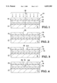
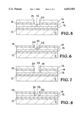
- FIGS. 1-6 illustrate the process of the invention for fabricating microgates with nano-filaments as shown in FIG. 6.
- FIGS. 1-4, 7, and 8 illustrate the process of the invention for the formation of microgates with nano-cones.
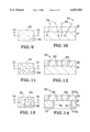
- FIGS. 9, 11, and 13 are plan views, with FIGS. 10, 12, and 14 being respective cross-sectional views illustrating operational steps in accordance with the invention for making a fused silica filter on silicon.
- the present invention is directed to vapor etching of nuclear tracks in dielectric materials for creating straight, high aspect ratio (i.e., length much greater than diameter), isolated cylindrical holes in the dielectric materials.
- the passage of an atomic particle through a dielectric material can result in the creation of a latent nuclear track that extends along a straight line corresponding to the path of the atomic particle.
- This latent track has a diameter of 5-20 nm with bonding and density different from the non-tracked region.
- there is a different etching rate of the tracked and non-tracked regions of the material and generally the shape of etched holes along the nuclear tracks previously have been conical with the largest diameter being near the surface.
- the etch rate in the latent track region must be very high compared to the non-tracked region. This is accomplished by the vapor etching process of the present invention, wherein independent control of the temperatures of the vapor and the tracked materials provide the means to vary separately the etch rates for the latent track regions and the non-tracked material.
- the vapor-etched holes can be enlarged and smoothed by subsequent dipping in a liquid etchant. This vapor etching process has been demonstrated for bulk fused silica and thermal fused silica and can be extended to other dielectric materials, such as polymers and silicon nitride.
- the 20-1000 nm diameter holes resulting from the vapor etching process are useful as molds for electroplating nanometer-sized filaments, as illustrated in FIG. 6, etching gate cavities for deposition of nano-cones, illustrated in FIG. 8, developing high-aspect ratio holes in trackable resists, and fused silica for the formation of molecular filters, as illustrated in FIG. 14.
- etching gate cavities for deposition of nano-cones illustrated in FIG. 8
- FIG. 14 fused silica for the formation of molecular filters, as illustrated in FIG. 14.
- the invention in addition to the invention being useful in the production of field emission cathodes in flat panel video displays, and the production of molecular filters for biological purposes, for cleaning of contaminated waste liquids, and for electrochemical separation purposes, it can be utilized wherever there is a need to form straight, high aspect ratio holes in dielectric materials, particularly where nuclear tracks in the dielectric materials are utilized.
- the process consists of cleaning the surface of the tracked material and exposing the cleaned surface to a vapor of a suitable etchant. Separate etch rates for the latent track regions and the non-tracked materials are provided by independent control of the temperatures of the vapor and of the tracked material.
- fused silica (SiO 2 ) glass layers are excellent dielectric isolation layers for microelectronics applications, such as field emission cathodes, and because fused silica is one of the most inert, non-reactive materials, it can be utilized in filters in a much broader range of liquids than conventionally used materials such as polycarbonate.
- the vapor etching process of the present invention enables the formation of straight, high aspect ratio holes in fused silica, thus enabling a wide use of this material.
- a device such as a field emission cathode, generally indicated at 10, comprises a substrate 11, composed of silicon, for example, a metal layer 12, composed of a nickel alloy, for example, a resistive layer 13, composed of a mixed oxide, for example, a dielectric or insulator layer 14, composed of fused silica, for example, a gate metal layer 15, composed of a nickel alloy with chromium overlayer, for example, and an insulator layer 16 composed of polycarbonate, for example.
- the substrate 11 may have a thickness of 0.7 to 1.1 mm and may be additionally composed of glass; the metal layer 12 may have a thickness of a few hundred nm; the resistive layer 13 may have a thickness of a few hundred nm; the dielectric or insulator layer 14 may have a thickness of a few hundred nm; the gate metal layer 15 may have a thickness of 50 to 200 nm; and the insulator layer 16, which may be composed of either a trackable resist or a hard mask, may have a thickness of 100 to 1000 nm, and if a trackable resist it can be composed of a dielectric polymer such as polycarbonate, and if a hard mask it can be composed of silicon nitride or fused silica.
- the treatment consists of exposing the surface of layer 16 to a vapor of a suitable etchant to form a hole 19 therein, see FIG. 2.
- the etchant is composed of 1:4 HF:H 2 O, with a vapor temperature of 24.5° C. with an equilibrium vapor pressure, and with the temperature of layer 16 being held at 31° C.
- Etching a hole 20 in the gate metal layer 15, see FIG. 3, is accomplished for example using standard reactive ion etching using the layer 16 as a mask.
- layer 14 is composed of SiO 2
- an etchant composed of 1:4 HF:H 2 O would be used for a time period of 1 hour at a vapor temperature of 24.5° C. with an equilibrium vapor pressure and with layer 14 being at a temperature of 31° C.
- Independent control of the temperatures of the vapor etchant and the tracked material provides the means to vary separately the etch rates for both the latent track regions and the non-tracked material, whereby a straight, high aspect ratio hole, such as hole 21 in FIG. 4 can be formed.
- the nanofilament 22 may be composed of nickel or platinum, having a length equal to the thickness of layer 14 and a diameter of 20 to 1000 nm.
- Removal of the layer 16 is accomplished by either the reactive ion etching process that puts the hole in layer 15 or by suitable dipping in liquid etchants.
- openings 36 are etched in the substrate, as shown in FIGS. 13 and 14, which forms a waffle-like support structure for the fused silica layer 32. This pattern is accomplished using conventional lithography, and then the exposed silicon is etched to form the opening 36 using standard liquid etchants.
- a fused silica filter is formed, and the diameter of the holes 35 is controlled by controlling the temperature of the vapor etch and the temperature of the fused silica layer 32 and the time of exposure to the vapor etchant.
- the temperature of the vapor etch may be 24.5° C. and the temperature of the fused silica layer may be 31° C.
Landscapes
- Chemical & Material Sciences (AREA)
- Life Sciences & Earth Sciences (AREA)
- Engineering & Computer Science (AREA)
- Chemical Kinetics & Catalysis (AREA)
- General Chemical & Material Sciences (AREA)
- Geochemistry & Mineralogy (AREA)
- Materials Engineering (AREA)
- Organic Chemistry (AREA)
- Physical Vapour Deposition (AREA)
- Drying Of Semiconductors (AREA)
Abstract
Description
Claims (24)
Priority Applications (1)
| Application Number | Priority Date | Filing Date | Title |
|---|---|---|---|
| US08/851,258 US6033583A (en) | 1997-05-05 | 1997-05-05 | Vapor etching of nuclear tracks in dielectric materials |
Applications Claiming Priority (1)
| Application Number | Priority Date | Filing Date | Title |
|---|---|---|---|
| US08/851,258 US6033583A (en) | 1997-05-05 | 1997-05-05 | Vapor etching of nuclear tracks in dielectric materials |
Publications (1)
| Publication Number | Publication Date |
|---|---|
| US6033583A true US6033583A (en) | 2000-03-07 |
Family
ID=25310361
Family Applications (1)
| Application Number | Title | Priority Date | Filing Date |
|---|---|---|---|
| US08/851,258 Expired - Lifetime US6033583A (en) | 1997-05-05 | 1997-05-05 | Vapor etching of nuclear tracks in dielectric materials |
Country Status (1)
| Country | Link |
|---|---|
| US (1) | US6033583A (en) |
Cited By (27)
| Publication number | Priority date | Publication date | Assignee | Title |
|---|---|---|---|---|
| US6365059B1 (en) | 2000-04-28 | 2002-04-02 | Alexander Pechenik | Method for making a nano-stamp and for forming, with the stamp, nano-size elements on a substrate |
| WO2002037564A2 (en) * | 2000-10-30 | 2002-05-10 | Gesellschaft für Schwerionenforschung mbH | Film material comprising metal spikes and method for the production thereof |
| US6444256B1 (en) * | 1999-11-17 | 2002-09-03 | The Regents Of The University Of California | Formation of nanometer-size wires using infiltration into latent nuclear tracks |
| US6503409B1 (en) * | 2000-05-25 | 2003-01-07 | Sandia Corporation | Lithographic fabrication of nanoapertures |
| US20040108136A1 (en) * | 2002-12-04 | 2004-06-10 | International Business Machines Corporation | Structure comprising a barrier layer of a tungsten alloy comprising cobalt and/or nickel |
| US20040195202A1 (en) * | 2000-04-28 | 2004-10-07 | Alexander Pechenik | Method for making a nano-stamp and for forming, with the stamp, nano-size elements on a substrate |
| WO2009115227A2 (en) * | 2008-03-20 | 2009-09-24 | Gsi Helmholtzzentrum Für Schwerionenforschung Gmbh | Nanowire structural element |
| US20100018852A1 (en) * | 2005-07-26 | 2010-01-28 | Dressel Pte. Ltd. | Process for Producing a Porous Track Membrane |
| US20120125893A1 (en) * | 2010-07-26 | 2012-05-24 | Hamamatsu Photonics K.K. | Laser processing method |
| US20150166396A1 (en) * | 2013-12-17 | 2015-06-18 | Corning Incorporated | Method for rapid laser drilling of holes in glass and products made therefrom |
| US20170189991A1 (en) * | 2014-07-14 | 2017-07-06 | Corning Incorporated | Systems and methods for processing transparent materials using adjustable laser beam focal lines |
| US10173916B2 (en) | 2013-12-17 | 2019-01-08 | Corning Incorporated | Edge chamfering by mechanically processing laser cut glass |
| US10252931B2 (en) | 2015-01-12 | 2019-04-09 | Corning Incorporated | Laser cutting of thermally tempered substrates |
| US10280108B2 (en) | 2013-03-21 | 2019-05-07 | Corning Laser Technologies GmbH | Device and method for cutting out contours from planar substrates by means of laser |
| US10335902B2 (en) | 2014-07-14 | 2019-07-02 | Corning Incorporated | Method and system for arresting crack propagation |
| US10421683B2 (en) | 2013-01-15 | 2019-09-24 | Corning Laser Technologies GmbH | Method and device for the laser-based machining of sheet-like substrates |
| US10522963B2 (en) | 2016-08-30 | 2019-12-31 | Corning Incorporated | Laser cutting of materials with intensity mapping optical system |
| US10525657B2 (en) | 2015-03-27 | 2020-01-07 | Corning Incorporated | Gas permeable window and method of fabricating the same |
| US10526234B2 (en) | 2014-07-14 | 2020-01-07 | Corning Incorporated | Interface block; system for and method of cutting a substrate being transparent within a range of wavelengths using such interface block |
| US10611667B2 (en) | 2014-07-14 | 2020-04-07 | Corning Incorporated | Method and system for forming perforations |
| US10626040B2 (en) | 2017-06-15 | 2020-04-21 | Corning Incorporated | Articles capable of individual singulation |
| US10752534B2 (en) | 2016-11-01 | 2020-08-25 | Corning Incorporated | Apparatuses and methods for laser processing laminate workpiece stacks |
| US11130701B2 (en) | 2016-09-30 | 2021-09-28 | Corning Incorporated | Apparatuses and methods for laser processing transparent workpieces using non-axisymmetric beam spots |
| US11542190B2 (en) | 2016-10-24 | 2023-01-03 | Corning Incorporated | Substrate processing station for laser-based machining of sheet-like glass substrates |
| US11556039B2 (en) | 2013-12-17 | 2023-01-17 | Corning Incorporated | Electrochromic coated glass articles and methods for laser processing the same |
| US11697178B2 (en) | 2014-07-08 | 2023-07-11 | Corning Incorporated | Methods and apparatuses for laser processing materials |
| US11773004B2 (en) | 2015-03-24 | 2023-10-03 | Corning Incorporated | Laser cutting and processing of display glass compositions |
Citations (10)
| Publication number | Priority date | Publication date | Assignee | Title |
|---|---|---|---|---|
| US3662178A (en) * | 1969-06-20 | 1972-05-09 | Gen Electric | Track-registration process |
| US3713921A (en) * | 1971-04-01 | 1973-01-30 | Gen Electric | Geometry control of etched nuclear particle tracks |
| US3770532A (en) * | 1971-02-16 | 1973-11-06 | Gen Electric | Porous bodies and method of making |
| US3802972A (en) * | 1968-06-27 | 1974-04-09 | Gen Electric | Process for making cylindrical holes in a sheet material |
| US4245229A (en) * | 1979-01-26 | 1981-01-13 | Exxon Research & Engineering Co. | Optical recording medium |
| US4338164A (en) * | 1979-12-20 | 1982-07-06 | Gesellschaft Fur Schwerionenforschung Gmbh | Method for producing planar surfaces having very fine peaks in the micron range |
| US5462467A (en) * | 1993-09-08 | 1995-10-31 | Silicon Video Corporation | Fabrication of filamentary field-emission device, including self-aligned gate |
| US5562516A (en) * | 1993-09-08 | 1996-10-08 | Silicon Video Corporation | Field-emitter fabrication using charged-particle tracks |
| US5580421A (en) * | 1994-06-14 | 1996-12-03 | Fsi International | Apparatus for surface conditioning |
| US5801477A (en) * | 1993-09-08 | 1998-09-01 | Candescent Technologies Corporation | Gated filament structures for a field emission display |
-
1997
- 1997-05-05 US US08/851,258 patent/US6033583A/en not_active Expired - Lifetime
Patent Citations (10)
| Publication number | Priority date | Publication date | Assignee | Title |
|---|---|---|---|---|
| US3802972A (en) * | 1968-06-27 | 1974-04-09 | Gen Electric | Process for making cylindrical holes in a sheet material |
| US3662178A (en) * | 1969-06-20 | 1972-05-09 | Gen Electric | Track-registration process |
| US3770532A (en) * | 1971-02-16 | 1973-11-06 | Gen Electric | Porous bodies and method of making |
| US3713921A (en) * | 1971-04-01 | 1973-01-30 | Gen Electric | Geometry control of etched nuclear particle tracks |
| US4245229A (en) * | 1979-01-26 | 1981-01-13 | Exxon Research & Engineering Co. | Optical recording medium |
| US4338164A (en) * | 1979-12-20 | 1982-07-06 | Gesellschaft Fur Schwerionenforschung Gmbh | Method for producing planar surfaces having very fine peaks in the micron range |
| US5462467A (en) * | 1993-09-08 | 1995-10-31 | Silicon Video Corporation | Fabrication of filamentary field-emission device, including self-aligned gate |
| US5562516A (en) * | 1993-09-08 | 1996-10-08 | Silicon Video Corporation | Field-emitter fabrication using charged-particle tracks |
| US5801477A (en) * | 1993-09-08 | 1998-09-01 | Candescent Technologies Corporation | Gated filament structures for a field emission display |
| US5580421A (en) * | 1994-06-14 | 1996-12-03 | Fsi International | Apparatus for surface conditioning |
Cited By (45)
| Publication number | Priority date | Publication date | Assignee | Title |
|---|---|---|---|---|
| US6444256B1 (en) * | 1999-11-17 | 2002-09-03 | The Regents Of The University Of California | Formation of nanometer-size wires using infiltration into latent nuclear tracks |
| US20040195202A1 (en) * | 2000-04-28 | 2004-10-07 | Alexander Pechenik | Method for making a nano-stamp and for forming, with the stamp, nano-size elements on a substrate |
| US6365059B1 (en) | 2000-04-28 | 2002-04-02 | Alexander Pechenik | Method for making a nano-stamp and for forming, with the stamp, nano-size elements on a substrate |
| US6503409B1 (en) * | 2000-05-25 | 2003-01-07 | Sandia Corporation | Lithographic fabrication of nanoapertures |
| WO2002037564A2 (en) * | 2000-10-30 | 2002-05-10 | Gesellschaft für Schwerionenforschung mbH | Film material comprising metal spikes and method for the production thereof |
| WO2002037564A3 (en) * | 2000-10-30 | 2002-11-07 | Schwerionenforsch Gmbh | Film material comprising metal spikes and method for the production thereof |
| US20040029413A1 (en) * | 2000-10-30 | 2004-02-12 | Norbert Angert | Film material comprising spikes and method for the production thereof |
| US6923651B2 (en) * | 2000-10-30 | 2005-08-02 | Gesellschaft Fuer Schwerionenforschung Mbh | Sheet material having metal points and method for the production thereof |
| US20040108136A1 (en) * | 2002-12-04 | 2004-06-10 | International Business Machines Corporation | Structure comprising a barrier layer of a tungsten alloy comprising cobalt and/or nickel |
| US20080237053A1 (en) * | 2002-12-04 | 2008-10-02 | International Business Machines Corporation | Structure comprising a barrier layer of a tungsten alloy comprising cobalt and/or nickel |
| US20100018852A1 (en) * | 2005-07-26 | 2010-01-28 | Dressel Pte. Ltd. | Process for Producing a Porous Track Membrane |
| US20160024673A1 (en) * | 2008-03-20 | 2016-01-28 | Gsi Helmholtzzentrum Fur Schwerionenforschung Gmbh | Nanowire Structural Element |
| WO2009115227A3 (en) * | 2008-03-20 | 2009-12-10 | Gsi Helmholtzzentrum Für Schwerionenforschung Gmbh | Nanowire structural element |
| US20110211994A1 (en) * | 2008-03-20 | 2011-09-01 | Thomas Cornelius | Nanowire Structural Element |
| US9222185B2 (en) | 2008-03-20 | 2015-12-29 | Gsi Helmholtzzentrum Fur Schwerionenforschung Gmbh | Nanowire structural element |
| US10301733B2 (en) * | 2008-03-20 | 2019-05-28 | Gsi Helmholtzzentrum Für Schwerionenforschung Gmbh | Nanowire structural element |
| WO2009115227A2 (en) * | 2008-03-20 | 2009-09-24 | Gsi Helmholtzzentrum Für Schwerionenforschung Gmbh | Nanowire structural element |
| US20120125893A1 (en) * | 2010-07-26 | 2012-05-24 | Hamamatsu Photonics K.K. | Laser processing method |
| US8961806B2 (en) * | 2010-07-26 | 2015-02-24 | Hamamatsu Photonics K.K. | Laser processing method |
| US11345625B2 (en) | 2013-01-15 | 2022-05-31 | Corning Laser Technologies GmbH | Method and device for the laser-based machining of sheet-like substrates |
| US11028003B2 (en) | 2013-01-15 | 2021-06-08 | Corning Laser Technologies GmbH | Method and device for laser-based machining of flat substrates |
| US10421683B2 (en) | 2013-01-15 | 2019-09-24 | Corning Laser Technologies GmbH | Method and device for the laser-based machining of sheet-like substrates |
| US11713271B2 (en) | 2013-03-21 | 2023-08-01 | Corning Laser Technologies GmbH | Device and method for cutting out contours from planar substrates by means of laser |
| US10280108B2 (en) | 2013-03-21 | 2019-05-07 | Corning Laser Technologies GmbH | Device and method for cutting out contours from planar substrates by means of laser |
| US10293436B2 (en) * | 2013-12-17 | 2019-05-21 | Corning Incorporated | Method for rapid laser drilling of holes in glass and products made therefrom |
| US10173916B2 (en) | 2013-12-17 | 2019-01-08 | Corning Incorporated | Edge chamfering by mechanically processing laser cut glass |
| US10144093B2 (en) | 2013-12-17 | 2018-12-04 | Corning Incorporated | Method for rapid laser drilling of holes in glass and products made therefrom |
| US10597321B2 (en) | 2013-12-17 | 2020-03-24 | Corning Incorporated | Edge chamfering methods |
| US11556039B2 (en) | 2013-12-17 | 2023-01-17 | Corning Incorporated | Electrochromic coated glass articles and methods for laser processing the same |
| US11148225B2 (en) | 2013-12-17 | 2021-10-19 | Corning Incorporated | Method for rapid laser drilling of holes in glass and products made therefrom |
| US20150166396A1 (en) * | 2013-12-17 | 2015-06-18 | Corning Incorporated | Method for rapid laser drilling of holes in glass and products made therefrom |
| US11697178B2 (en) | 2014-07-08 | 2023-07-11 | Corning Incorporated | Methods and apparatuses for laser processing materials |
| US10335902B2 (en) | 2014-07-14 | 2019-07-02 | Corning Incorporated | Method and system for arresting crack propagation |
| US20170189991A1 (en) * | 2014-07-14 | 2017-07-06 | Corning Incorporated | Systems and methods for processing transparent materials using adjustable laser beam focal lines |
| US10526234B2 (en) | 2014-07-14 | 2020-01-07 | Corning Incorporated | Interface block; system for and method of cutting a substrate being transparent within a range of wavelengths using such interface block |
| US10611667B2 (en) | 2014-07-14 | 2020-04-07 | Corning Incorporated | Method and system for forming perforations |
| US11648623B2 (en) * | 2014-07-14 | 2023-05-16 | Corning Incorporated | Systems and methods for processing transparent materials using adjustable laser beam focal lines |
| US10252931B2 (en) | 2015-01-12 | 2019-04-09 | Corning Incorporated | Laser cutting of thermally tempered substrates |
| US11773004B2 (en) | 2015-03-24 | 2023-10-03 | Corning Incorporated | Laser cutting and processing of display glass compositions |
| US10525657B2 (en) | 2015-03-27 | 2020-01-07 | Corning Incorporated | Gas permeable window and method of fabricating the same |
| US10522963B2 (en) | 2016-08-30 | 2019-12-31 | Corning Incorporated | Laser cutting of materials with intensity mapping optical system |
| US11130701B2 (en) | 2016-09-30 | 2021-09-28 | Corning Incorporated | Apparatuses and methods for laser processing transparent workpieces using non-axisymmetric beam spots |
| US11542190B2 (en) | 2016-10-24 | 2023-01-03 | Corning Incorporated | Substrate processing station for laser-based machining of sheet-like glass substrates |
| US10752534B2 (en) | 2016-11-01 | 2020-08-25 | Corning Incorporated | Apparatuses and methods for laser processing laminate workpiece stacks |
| US10626040B2 (en) | 2017-06-15 | 2020-04-21 | Corning Incorporated | Articles capable of individual singulation |
Similar Documents
| Publication | Publication Date | Title |
|---|---|---|
| US6033583A (en) | Vapor etching of nuclear tracks in dielectric materials | |
| KR900003256B1 (en) | Method of removing photo resist on a semiconductor wafer | |
| US4405710A (en) | Ion beam exposure of (g-Gex -Se1-x) inorganic resists | |
| EP0020776B1 (en) | Method of forming patterns | |
| US5580615A (en) | Method of forming a conductive film on an insulating region of a substrate | |
| EP0984327A2 (en) | Process for producing halftone mask | |
| JPS5812344B2 (en) | Method for forming metal patterns using copper as a base material | |
| JP5264237B2 (en) | Nanostructure and method for producing nanostructure | |
| JP2988455B2 (en) | Plasma etching method | |
| US5755947A (en) | Adhesion enhancement for underplating problem | |
| NL8202103A (en) | METHOD FOR ETCHING TANTALUM AND SILICON CONTAINING USING REACTIVE ION | |
| JP3554009B2 (en) | Mask plate for forming fine pattern and method of manufacturing the same | |
| JPS58169150A (en) | Manufacture of photomask | |
| JPS62136025A (en) | Ultrafine pattern working carbon film and working method for ultrafine pattern | |
| JPH08297361A (en) | Transfer mask | |
| JPH05160078A (en) | Dry etching method | |
| US6261961B1 (en) | Adhesion layer for etching of tracks in nuclear trackable materials | |
| US6709605B2 (en) | Etching method | |
| JP3246849B2 (en) | Transfer mask | |
| JPS6024933B2 (en) | Electron sensitive inorganic resist | |
| JPH0950968A (en) | Manufacture of semiconductor element and semiconductor element | |
| JP3104727B2 (en) | Aperture manufacturing method | |
| JPS5946748A (en) | Ion shower unit | |
| JP2004272049A (en) | METHOD FOR FORMING SOLID COMPOUND FILM CONTAINING Si-O-Si BOND, MODIFICATION METHOD OF SOLID COMPOUND FILM INTO SILICON OXIDE, METHOD FOR FORMING PATTERN, AND LITHOGRAPHIC RESIST | |
| JPH0247848B2 (en) |
Legal Events
| Date | Code | Title | Description |
|---|---|---|---|
| AS | Assignment |
Owner name: REGENTS OF THE UNIVERSITY OF CALIFORNIA, THE, CALI Free format text: ASSIGNMENT OF ASSIGNORS INTEREST;ASSIGNORS:MUSKET, RONALD G.;PORTER, JOHN D.;YOSHIYAMA, JAMES M.;AND OTHERS;REEL/FRAME:008541/0508;SIGNING DATES FROM 19970130 TO 19970411 |
|
| AS | Assignment |
Owner name: CANDESCENT TECHNOLOGIES CORPORATION, CALIFORNIA Free format text: ASSIGNMENT OF ASSIGNORS INTEREST;ASSIGNOR:PORTER, JOHN D.;REEL/FRAME:009281/0921 Effective date: 19970214 |
|
| AS | Assignment |
Owner name: U.S. DEPARTMENT OF ENERGY, CALIFORNIA Free format text: CONFIRMATORY LICENSE;ASSIGNOR:CALIFORNIA, UNIVERSITY OF;REEL/FRAME:009832/0153 Effective date: 19980601 |
|
| STCF | Information on status: patent grant |
Free format text: PATENTED CASE |
|
| AS | Assignment |
Owner name: REGENTS OF THE UNIVERSITY OF CALIFORNIA, THE, CALI Free format text: ASSIGNMENT OF ASSIGNORS INTEREST;ASSIGNORS:REGENTS OF THE UNIVERSITY OF CALIFORNIA, THE;CANDESCENT TECHNOLOGIES CORPORATION;REEL/FRAME:010996/0955 Effective date: 20000725 Owner name: CANDESCENT TECHNOLOGIES CORPORATION, CALIFORNIA Free format text: ASSIGNMENT OF ASSIGNORS INTEREST;ASSIGNORS:REGENTS OF THE UNIVERSITY OF CALIFORNIA, THE;CANDESCENT TECHNOLOGIES CORPORATION;REEL/FRAME:010996/0955 Effective date: 20000725 |
|
| AS | Assignment |
Owner name: ENERGY, U.S. DEPARTMENT OF, CALIFORNIA Free format text: CONFIRMATORY LICENSE;ASSIGNOR:CANDESCENT TECHNOLOGIES CORPORATION;REEL/FRAME:011379/0495 Effective date: 20000519 |
|
| AS | Assignment |
Owner name: CANDESCENT INTELLECTUAL PROPERTY SERVICES, INC., C Free format text: ASSIGNMENT OF ASSIGNORS INTEREST;ASSIGNOR:CANDESCENT TECHNOLOGIES CORPORATION;REEL/FRAME:011857/0343 Effective date: 20001205 |
|
| REMI | Maintenance fee reminder mailed | ||
| FPAY | Fee payment |
Year of fee payment: 4 |
|
| SULP | Surcharge for late payment | ||
| AS | Assignment |
Owner name: CANDESCENT TECHNOLOGIES CORPORATION, CALIFORNIA Free format text: CORRECTIVE ASSIGNMENT TO CORRECT THE ASSIGNEES. THE NAME OF AN ASSIGNEE WAS INADVERTENTLY OMITTED FROM THE RECORDATION FORM COVER SHEET PREVIOUSLY RECORDED ON REEL 011857 FRAME 0343;ASSIGNOR:CANDESCENT TECHNOLOGIES CORPORATION;REEL/FRAME:018411/0715 Effective date: 20001205 Owner name: CANDESCENT INTELLECTUAL PROPERTY SERVICES, INC., C Free format text: CORRECTIVE ASSIGNMENT TO CORRECT THE ASSIGNEES. THE NAME OF AN ASSIGNEE WAS INADVERTENTLY OMITTED FROM THE RECORDATION FORM COVER SHEET PREVIOUSLY RECORDED ON REEL 011857 FRAME 0343;ASSIGNOR:CANDESCENT TECHNOLOGIES CORPORATION;REEL/FRAME:018411/0715 Effective date: 20001205 |
|
| AS | Assignment |
Owner name: CANON KABUSHIKI KAISHA, JAPAN Free format text: NUNC PRO TUNC ASSIGNMENT EFFECTIVE AS OF AUGUST 26, 2004;ASSIGNOR:CANDESCENT TECHNOLOGIES CORPORATION;REEL/FRAME:019466/0437 Effective date: 20070104 |
|
| AS | Assignment |
Owner name: CANON KABUSHIKI KAISHA, JAPAN Free format text: NUNC PRO TUNC ASSIGNMENT;ASSIGNOR:CANDESCENT INTELLECTUAL PROPERTY SERVICES, INC.;REEL/FRAME:019580/0723 Effective date: 20061226 |
|
| REMI | Maintenance fee reminder mailed | ||
| FEPP | Fee payment procedure |
Free format text: PAT HOLDER NO LONGER CLAIMS SMALL ENTITY STATUS, ENTITY STATUS SET TO UNDISCOUNTED (ORIGINAL EVENT CODE: STOL); ENTITY STATUS OF PATENT OWNER: LARGE ENTITY |
|
| REFU | Refund |
Free format text: REFUND - PAYMENT OF MAINTENANCE FEE, 8TH YR, SMALL ENTITY (ORIGINAL EVENT CODE: R2552); ENTITY STATUS OF PATENT OWNER: LARGE ENTITY Free format text: REFUND - 7.5 YR SURCHARGE - LATE PMT W/IN 6 MO, SMALL ENTITY (ORIGINAL EVENT CODE: R2555); ENTITY STATUS OF PATENT OWNER: LARGE ENTITY |
|
| FPAY | Fee payment |
Year of fee payment: 8 |
|
| SULP | Surcharge for late payment |
Year of fee payment: 7 |
|
| AS | Assignment |
Owner name: LAWRENCE LIVERMORE NATIONAL SECURITY LLC, CALIFORN Free format text: ASSIGNMENT OF ASSIGNORS INTEREST;ASSIGNOR:THE REGENTS OF THE UNIVERSITY OF CALIFORNIA;REEL/FRAME:021217/0050 Effective date: 20080623 |
|
| FPAY | Fee payment |
Year of fee payment: 12 |