JP4391857B2 - Pixel circuit of organic light emitting display and driving method thereof - Google Patents
Pixel circuit of organic light emitting display and driving method thereof Download PDFInfo
- Publication number
- JP4391857B2 JP4391857B2 JP2004066129A JP2004066129A JP4391857B2 JP 4391857 B2 JP4391857 B2 JP 4391857B2 JP 2004066129 A JP2004066129 A JP 2004066129A JP 2004066129 A JP2004066129 A JP 2004066129A JP 4391857 B2 JP4391857 B2 JP 4391857B2
- Authority
- JP
- Japan
- Prior art keywords
- transistor
- source
- current
- drain
- signal
- Prior art date
- Legal status (The legal status is an assumption and is not a legal conclusion. Google has not performed a legal analysis and makes no representation as to the accuracy of the status listed.)
- Expired - Lifetime
Links
- 238000000034 method Methods 0.000 title claims description 16
- 239000003990 capacitor Substances 0.000 claims description 34
- 230000005684 electric field Effects 0.000 claims 1
- 239000004065 semiconductor Substances 0.000 claims 1
- 238000005401 electroluminescence Methods 0.000 description 36
- 239000010409 thin film Substances 0.000 description 10
- 238000010586 diagram Methods 0.000 description 9
- 238000004519 manufacturing process Methods 0.000 description 5
- 229920001621 AMOLED Polymers 0.000 description 4
- 239000011159 matrix material Substances 0.000 description 3
- 230000015556 catabolic process Effects 0.000 description 2
- 238000006731 degradation reaction Methods 0.000 description 2
- 238000001514 detection method Methods 0.000 description 1
- 230000000694 effects Effects 0.000 description 1
- 230000003071 parasitic effect Effects 0.000 description 1
- 239000000758 substrate Substances 0.000 description 1
Images


Classifications
-
- G—PHYSICS
- G09—EDUCATION; CRYPTOGRAPHY; DISPLAY; ADVERTISING; SEALS
- G09G—ARRANGEMENTS OR CIRCUITS FOR CONTROL OF INDICATING DEVICES USING STATIC MEANS TO PRESENT VARIABLE INFORMATION
- G09G3/00—Control arrangements or circuits, of interest only in connection with visual indicators other than cathode-ray tubes
- G09G3/20—Control arrangements or circuits, of interest only in connection with visual indicators other than cathode-ray tubes for presentation of an assembly of a number of characters, e.g. a page, by composing the assembly by combination of individual elements arranged in a matrix no fixed position being assigned to or needed to be assigned to the individual characters or partial characters
- G09G3/22—Control arrangements or circuits, of interest only in connection with visual indicators other than cathode-ray tubes for presentation of an assembly of a number of characters, e.g. a page, by composing the assembly by combination of individual elements arranged in a matrix no fixed position being assigned to or needed to be assigned to the individual characters or partial characters using controlled light sources
- G09G3/30—Control arrangements or circuits, of interest only in connection with visual indicators other than cathode-ray tubes for presentation of an assembly of a number of characters, e.g. a page, by composing the assembly by combination of individual elements arranged in a matrix no fixed position being assigned to or needed to be assigned to the individual characters or partial characters using controlled light sources using electroluminescent panels
- G09G3/32—Control arrangements or circuits, of interest only in connection with visual indicators other than cathode-ray tubes for presentation of an assembly of a number of characters, e.g. a page, by composing the assembly by combination of individual elements arranged in a matrix no fixed position being assigned to or needed to be assigned to the individual characters or partial characters using controlled light sources using electroluminescent panels semiconductive, e.g. using light-emitting diodes [LED]
- G09G3/3208—Control arrangements or circuits, of interest only in connection with visual indicators other than cathode-ray tubes for presentation of an assembly of a number of characters, e.g. a page, by composing the assembly by combination of individual elements arranged in a matrix no fixed position being assigned to or needed to be assigned to the individual characters or partial characters using controlled light sources using electroluminescent panels semiconductive, e.g. using light-emitting diodes [LED] organic, e.g. using organic light-emitting diodes [OLED]
- G09G3/3225—Control arrangements or circuits, of interest only in connection with visual indicators other than cathode-ray tubes for presentation of an assembly of a number of characters, e.g. a page, by composing the assembly by combination of individual elements arranged in a matrix no fixed position being assigned to or needed to be assigned to the individual characters or partial characters using controlled light sources using electroluminescent panels semiconductive, e.g. using light-emitting diodes [LED] organic, e.g. using organic light-emitting diodes [OLED] using an active matrix
- G09G3/3233—Control arrangements or circuits, of interest only in connection with visual indicators other than cathode-ray tubes for presentation of an assembly of a number of characters, e.g. a page, by composing the assembly by combination of individual elements arranged in a matrix no fixed position being assigned to or needed to be assigned to the individual characters or partial characters using controlled light sources using electroluminescent panels semiconductive, e.g. using light-emitting diodes [LED] organic, e.g. using organic light-emitting diodes [OLED] using an active matrix with pixel circuitry controlling the current through the light-emitting element
-
- G—PHYSICS
- G09—EDUCATION; CRYPTOGRAPHY; DISPLAY; ADVERTISING; SEALS
- G09G—ARRANGEMENTS OR CIRCUITS FOR CONTROL OF INDICATING DEVICES USING STATIC MEANS TO PRESENT VARIABLE INFORMATION
- G09G2300/00—Aspects of the constitution of display devices
- G09G2300/08—Active matrix structure, i.e. with use of active elements, inclusive of non-linear two terminal elements, in the pixels together with light emitting or modulating elements
- G09G2300/0809—Several active elements per pixel in active matrix panels
- G09G2300/0819—Several active elements per pixel in active matrix panels used for counteracting undesired variations, e.g. feedback or autozeroing
-
- G—PHYSICS
- G09—EDUCATION; CRYPTOGRAPHY; DISPLAY; ADVERTISING; SEALS
- G09G—ARRANGEMENTS OR CIRCUITS FOR CONTROL OF INDICATING DEVICES USING STATIC MEANS TO PRESENT VARIABLE INFORMATION
- G09G2300/00—Aspects of the constitution of display devices
- G09G2300/08—Active matrix structure, i.e. with use of active elements, inclusive of non-linear two terminal elements, in the pixels together with light emitting or modulating elements
- G09G2300/0809—Several active elements per pixel in active matrix panels
- G09G2300/0842—Several active elements per pixel in active matrix panels forming a memory circuit, e.g. a dynamic memory with one capacitor
- G09G2300/0861—Several active elements per pixel in active matrix panels forming a memory circuit, e.g. a dynamic memory with one capacitor with additional control of the display period without amending the charge stored in a pixel memory, e.g. by means of additional select electrodes
-
- G—PHYSICS
- G09—EDUCATION; CRYPTOGRAPHY; DISPLAY; ADVERTISING; SEALS
- G09G—ARRANGEMENTS OR CIRCUITS FOR CONTROL OF INDICATING DEVICES USING STATIC MEANS TO PRESENT VARIABLE INFORMATION
- G09G2310/00—Command of the display device
- G09G2310/02—Addressing, scanning or driving the display screen or processing steps related thereto
- G09G2310/0243—Details of the generation of driving signals
- G09G2310/0251—Precharge or discharge of pixel before applying new pixel voltage
-
- G—PHYSICS
- G09—EDUCATION; CRYPTOGRAPHY; DISPLAY; ADVERTISING; SEALS
- G09G—ARRANGEMENTS OR CIRCUITS FOR CONTROL OF INDICATING DEVICES USING STATIC MEANS TO PRESENT VARIABLE INFORMATION
- G09G2310/00—Command of the display device
- G09G2310/02—Addressing, scanning or driving the display screen or processing steps related thereto
- G09G2310/0262—The addressing of the pixel, in a display other than an active matrix LCD, involving the control of two or more scan electrodes or two or more data electrodes, e.g. pixel voltage dependent on signals of two data electrodes
-
- G—PHYSICS
- G09—EDUCATION; CRYPTOGRAPHY; DISPLAY; ADVERTISING; SEALS
- G09G—ARRANGEMENTS OR CIRCUITS FOR CONTROL OF INDICATING DEVICES USING STATIC MEANS TO PRESENT VARIABLE INFORMATION
- G09G2320/00—Control of display operating conditions
- G09G2320/04—Maintaining the quality of display appearance
- G09G2320/043—Preventing or counteracting the effects of ageing
- G09G2320/045—Compensation of drifts in the characteristics of light emitting or modulating elements
Landscapes
- Engineering & Computer Science (AREA)
- Physics & Mathematics (AREA)
- Computer Hardware Design (AREA)
- General Physics & Mathematics (AREA)
- Theoretical Computer Science (AREA)
- Control Of Indicators Other Than Cathode Ray Tubes (AREA)
- Control Of El Displays (AREA)
- Electroluminescent Light Sources (AREA)
Description
本発明は、平板表示装置に関し、より詳しくは、EL(Electro luminescence)素子を駆動するトランジスタのスレショルド電圧を自ら補償することによって、高い階調を実現できる有機電界発光表示装置の画素回路及びその駆動方法に関する。 The present invention relates to a flat panel display device, and more specifically, a pixel circuit of an organic light emitting display device capable of realizing high gradation by self-compensating a threshold voltage of a transistor driving an EL (Electro luminescence) element, and driving thereof Regarding the method.
通常、有機電界発光表示装置は、EL素子を駆動する方式によってパッシブマトリクス型OLED(Organic Light-Emitting Diode)と、アクティブマトリクス型OLEDとに分けられ、電流駆動方式のOLEDと電圧駆動方式のOLEDとに分けられる。 In general, the organic light emitting display device is divided into a passive matrix type OLED (Organic Light-Emitting Diode) and an active matrix type OLED according to a method of driving an EL element, and a current driving type OLED and a voltage driving type OLED. It is divided into.
AMOLED(Active Matrix Organic Light Emitting Diode)は、複数のゲートライン、複数のデータライン及び複数の電源ラインと、前記ラインに接続され、マトリクス形態で配列される複数の画素とを備える。各画素は、通常、EL素子と、2つのトランジスタ、すなわちデータ信号を伝達するためのスイッチングトランジスタ及び前記データ信号によって前記EL素子を駆動させるための駆動トランジスタと、前記データ電圧を維持させるための1つのコンデンサとで構成される。 An AMOLED (Active Matrix Organic Light Emitting Diode) includes a plurality of gate lines, a plurality of data lines, and a plurality of power supply lines, and a plurality of pixels connected to the lines and arranged in a matrix form. Each pixel usually includes an EL element, two transistors, a switching transistor for transmitting a data signal, a driving transistor for driving the EL element by the data signal, and a 1 for maintaining the data voltage. Consists of two capacitors.
このようなAMOLEDは、消費電力が少ないという利点があるが、時間によってEL素子を介して流れる電流強度が変わり、表示ムラを招く問題点があった。これは、EL素子を駆動する駆動トランジスタのゲートとソース間の電圧、すなわち駆動トランジスタのスレショルド電圧(threshold voltage)が変わり、EL素子を介して流れる電流が変わるからである。 Such an AMOLED has an advantage of low power consumption, but there is a problem in that the intensity of current flowing through the EL element varies depending on time, resulting in display unevenness. This is because the voltage between the gate and the source of the driving transistor for driving the EL element, that is, the threshold voltage of the driving transistor changes, and the current flowing through the EL element changes.
すなわち前記駆動トランジスタ用薄膜トランジスタは、製造工程変数によってスレショルド電圧が変わるので、AMOLEDの全てのトランジスタのスレショルド電圧が同一になるように、トランジスタを製造することが難しくて、これにより、画素間にスレショルド電圧の変動が存在するからである。 That is, since the threshold voltage of the driving transistor thin film transistor varies depending on manufacturing process variables, it is difficult to manufacture the transistors so that the threshold voltages of all the transistors of the AMOLED are the same. This is because there are fluctuations.
このような問題を解決するために、スレショルド電圧補償用トランジスタを追加して、製造工程変数によるスレショルド電圧を補償する方法があった。米国特許第6、229、506号明細書には、スレショルド電圧の変動を補償するための有機電界発光表示装置が開示されている。この米国特許第6、229、506号明細書には、電流ソースが駆動トランジスタのオーバードライブ電圧(overdrive voltage)に対してソース−ゲート間電圧を調節し、駆動トランジスタのスレショルド電圧の変動を補償する画素構造が開示されている。前記米国特許第6、229、506号明細書の有機電界発光表示装置は、データロード(データ書込み)段階及び連続的な発光段階の2段階動作を行うものであって、電流ソースがオーバードライブ電圧に対して駆動トランジスタのソース−ゲート間の電圧を調整し、駆動トランジスタのスレショルド電圧の変動を補償した。 In order to solve such a problem, there has been a method of adding a threshold voltage compensating transistor to compensate a threshold voltage due to a manufacturing process variable. US Pat. No. 6,229,506 discloses an organic light emitting display for compensating for threshold voltage variations. In US Pat. No. 6,229,506, the current source adjusts the source-gate voltage with respect to the overdrive voltage of the driving transistor to compensate for variations in the threshold voltage of the driving transistor. A pixel structure is disclosed. The organic light emitting display of US Pat. No. 6,229,506 performs a two-stage operation of a data load stage and a continuous light emission stage, and the current source is an overdrive voltage. In contrast, the voltage between the source and gate of the driving transistor was adjusted to compensate for the variation in the threshold voltage of the driving transistor.
しかし、上述したような有機電界発光表示装置は、電流ソースから印加される電流レベルのデータ信号によってEL素子を駆動する電流駆動方式のものであって、データラインをチャージ(charge)することが困難であった。すなわち、データラインの寄生キャパシタンスは相対的に大きく、電流ソースから提供されるデータ信号の電流レベルは相対的に小さいため、データラインをチャージするのにかなり長時間を要するばかりでなく、データが不安定となる問題点があった。 However, the organic light emitting display as described above is of a current driving type in which an EL element is driven by a data signal of a current level applied from a current source, and it is difficult to charge a data line. Met. That is, since the parasitic capacitance of the data line is relatively large and the current level of the data signal provided from the current source is relatively small, not only does it take a considerable amount of time to charge the data line, but the data is not good. There was a problem that became stable.
上述したような電流駆動方式のデータラインチャージ問題を解決するために、ミラータイプの画素構造を有する有機電界発光表示装置が提案された。図7は、従来の電圧駆動方式の有機電界発光表示装置においてミラータイプを有する電圧駆動方式の画素回路を示す図である。 In order to solve the current-driven data line charge problem as described above, an organic light emitting display device having a mirror type pixel structure has been proposed. FIG. 7 is a diagram illustrating a voltage-driven pixel circuit having a mirror type in a conventional voltage-driven organic light emitting display device.
図7を参照すれば、複数のゲートライン、すなわち複数のスキャンラインのうち該当するスキャンラインに印加される現在スキャン信号scan[n]にゲートが接続され、複数のデータラインのうち該当するデータラインに印加されるデータ信号VDATAmがソースに印加されるp型の第1のトランジスタT11と、前記現在のスキャンラインのすぐ前のスキャンラインに印加される以前スキャン信号scan[n−1]がゲートに印加され、ドレインに初期化電圧Vintiが印加されるp型の第2のトランジスタT12と、ミラー形態を有するp型の第3及び第4のトランジスタT13、T14と、前記以前スキャン信号scan[n−1]がゲートに印加され、ドレインが前記第4のトランジスタT14のドレインに接続されるn型の第5のトランジスタT15と、前記第5のトランジスタT15と接地電圧VSSとの間に接続されるEL素子EL11と、前記第4のトランジスタT14のゲート−ソース間に接続される第1のコンデンサC11とを備える。 Referring to FIG. 7, a gate is connected to a current scan signal scan [n] applied to a corresponding scan line among a plurality of gate lines, that is, a plurality of scan lines, and the corresponding data line is selected from the plurality of data lines. The p-type first transistor T11 to which the data signal VDATAm applied to the source is applied to the source, and the previous scan signal scan [n−1] applied to the scan line immediately before the current scan line are supplied to the gate. A p-type second transistor T12 having a drain applied with an initialization voltage Vinti; p-type third and fourth transistors T13 and T14 having a mirror configuration; and the previous scan signal scan [n− 1] is applied to the gate and the drain is connected to the drain of the fourth transistor T14 The fifth transistor T15, the EL element EL11 connected between the fifth transistor T15 and the ground voltage VSS, and the first capacitor C11 connected between the gate and source of the fourth transistor T14. With.
以下では、上述したような構造を有する有機電界発光表示装置の画素の動作を図8の動作波形図を参照して説明する。この際、現在駆動しようとするスキャンラインがn番目のスキャンラインであり、前記n番目のスキャンラインに印加されるスキャン信号がscan[n]であり、現在スキャンラインの以前に駆動されるスキャンラインがn−1番目のスキャンラインであり、前記n−1番目のスキャンラインに印加されるスキャン信号をscan[n−1]と言う。 Hereinafter, the operation of the pixel of the organic light emitting display having the above-described structure will be described with reference to the operation waveform diagram of FIG. At this time, the scan line to be driven is the nth scan line, the scan signal applied to the nth scan line is scan [n], and the scan line is driven before the current scan line. Is the (n-1) th scan line, and the scan signal applied to the (n-1) th scan line is referred to as scan [n-1].
まず、初期化動作時には、所定レベルの以前スキャン信号scan[n−1]及び現在スキャン信号scan[n]が印加されると、すなわちロウレベルの以前スキャン信号scan[n−1]とハイレベルの現在スキャン信号scan[n]が印加されると、トランジスタT12がオン(ON)となり、トランジスタT11、T15がオフ(OFF)となり、ミラータイプのトランジスタT13、T14がオフ(OFF)となる。したがって、コンデンサC11に格納されたデータは、トランジスタT12を介して初期化電圧Vintiにより初期化される。 First, during the initialization operation, when the previous scan signal scan [n−1] and the current scan signal scan [n] of a predetermined level are applied, that is, the low level previous scan signal scan [n−1] and the high level current scan signal. When the scan signal scan [n] is applied, the transistor T12 is turned on, the transistors T11 and T15 are turned off, and the mirror type transistors T13 and T14 are turned off. Therefore, the data stored in the capacitor C11 is initialized by the initialization voltage Vinti through the transistor T12.
一方、データプログラムの時には、所定レベルの以前スキャン信号scan[n−1]及び現在スキャン信号が印加されると、すなわちハイレベルの以前スキャン信号scan[n−1]とロウレベルの現在スキャン信号scan[n]が印加されると、トランジスタT12は、オフとなり、トランジスタT11がオンとなり、ミラータイプのトランジスタT13、T14がオンとなる。 On the other hand, at the time of data programming, when a previous level scan signal scan [n-1] and a current scan signal are applied, that is, a high level previous scan signal scan [n-1] and a low level current scan signal scan [n-1]. n] is applied, the transistor T12 is turned off, the transistor T11 is turned on, and the mirror type transistors T13 and T14 are turned on.
したがって、データラインに印加される電圧レベルのデータ信号VDATAmがトランジスタT13を介して駆動トランジスタT14のゲートに伝達される。この際、以前スキャン信号scan[n−1]によりトランジスタT15がオンとなるので、駆動トランジスタT14のゲートに印加される電圧レベルのデータ信号VDATAmに対応する駆動電流がEL素子EL11に流れ、発光するようになる。 Therefore, the voltage level data signal VDATAm applied to the data line is transmitted to the gate of the driving transistor T14 via the transistor T13. At this time, since the transistor T15 is turned on by the previous scan signal scan [n−1], the drive current corresponding to the voltage level data signal VDATAm applied to the gate of the drive transistor T14 flows to the EL element EL11 to emit light. It becomes like this.
前記トランジスタT14のゲートに印加される電圧は、VDATA−VTH(T13)となり、EL素子EL11を介して流れる電流は、下記の式(1)で表される。

上記数1中、IEL11は有機EL素子EL11に流れる電流、VGS(T14)はトランジスタT14のソースとゲート間の電圧、VTH(13)はトランジスタT13のスレショルド電圧、VDATAはデータ電圧、βは定数値を各々示す。 In Equation 1, I EL11 is a current flowing through the organic EL element EL11, V GS (T14) is a voltage between the source and gate of the transistor T14, V TH (13) is a threshold voltage of the transistor T13, V DATA is a data voltage, β represents a constant value.
この際、電流ミラー用トランジスタT13、T14のスレショルド電圧が同じならば、すなわちVTH(T13)=VTH(T14)の場合、トランジスタのスレショルド電圧を補償できるので、EL素子EL11の駆動電流を均一に維持できる。 At this time, if the threshold voltages of the current mirror transistors T13 and T14 are the same, that is, if V TH (T13) = V TH (T14) , the threshold voltage of the transistor can be compensated, so that the drive current of the EL element EL11 is made uniform. Can be maintained.
しかしながら、上述したような電流ミラー型電圧駆動方式では、電流ミラーを構成するトランジスタT13、T14が互いに隣接して基板上に配列されても、TFTの製造工程変数により同じスレショルド電圧を得ることは非常に難しい。したがって、TFTのスレショルド電圧の変動により均一な駆動電流を得ることが難しく、これにより、画質劣化を招く問題点があった。 However, in the current mirror type voltage driving method as described above, even if the transistors T13 and T14 constituting the current mirror are arranged adjacent to each other on the substrate, it is very difficult to obtain the same threshold voltage due to the manufacturing process variables of the TFT. It is difficult. Therefore, it is difficult to obtain a uniform drive current due to fluctuations in the threshold voltage of the TFT, and this causes a problem of image quality degradation.
上述したような電流ミラータイプの電圧駆動方式において、電流ミラー用TFT間スレショルド電圧の変動による画質劣化問題を解決するための技術が米国特許第6、362、798号明細書に開示されている。この米国特許第6、362、798号明細書は、駆動トランジスタのスレショルド電圧を補償するために、ダイオード形態の補償用薄膜トランジスタを駆動トランジスタのゲートに接続して構成した。しかし、前記米国特許第6、362、798号明細書でも補償用薄膜トランジスタとEL素子駆動用薄膜トランジスタのスレショルド電圧が同一でない場合、駆動トランジスタのスレショルド電圧の変動が補償されない問題点があった。
したがって、本発明は、上述したような従来技術の問題点を解決するためになされたもので、スレショルド電圧の変動を検出して、自ら補償(self-compensation)できる有機電界発光表示装置の画素回路及びその駆動方法を提供することにある。 Accordingly, the present invention has been made to solve the above-described problems of the prior art, and is a pixel circuit of an organic light emitting display that can detect a threshold voltage variation and can self-compensate. And providing a driving method thereof.
また、本発明の他の目的は、製造工程変数に関係なくスレショルド電圧の変動を補償できる有機電界発光表示装置の画素回路及びその駆動方法を提供することにある。 Another object of the present invention is to provide a pixel circuit of an organic light emitting display device and a driving method thereof that can compensate for variations in threshold voltage regardless of manufacturing process variables.
また、本発明のさらに他の目的は、各画素間のスレショルド電圧の変動に関係なくEL素子を介して均一な駆動電流が流れるようにすることができる有機電界発光表示装置の画素回路及びその駆動方法を提供することにある。 Still another object of the present invention is to provide a pixel circuit of an organic light emitting display device and a driving method thereof in which a uniform driving current can flow through an EL element regardless of a change in threshold voltage between pixels. It is to provide a method.
また、本発明のさらに他の目的は、各画素間のスレショルド電圧の変動に関係なく高い階調を実現できる有機電界発光表示装置の画素回路及びその駆動方法を提供することにある。 Another object of the present invention is to provide a pixel circuit of an organic light emitting display device and a driving method thereof that can realize a high gradation regardless of a change in threshold voltage between pixels.
前記目的を達成するために、本発明の一態様による有機電界発光表示装置の画素回路は、現在スキャンライン信号に応答して電圧レベルのデータ信号を伝達する第1のトランジスタと、前記第1のトランジスタを介して伝達される電圧レベルのデータ信号によって駆動電流を発生する第2のトランジスタと、前記第2のトランジスタのスレショルド電圧の変動を検出して自ら補償するための第3のトランジスタと、前記第2のトランジスタに伝達される電圧レベルのデータ信号を格納するためのコンデンサと、前記第2のトランジスタを介して発生する駆動電流に対応して光を発光するEL素子とを備えることを特徴とする。 In order to achieve the above object, a pixel circuit of an organic light emitting display according to an aspect of the present invention includes a first transistor that transmits a data signal having a voltage level in response to a current scan line signal, and the first transistor. A second transistor that generates a drive current according to a data signal at a voltage level transmitted through the transistor, a third transistor for detecting and compensating for the threshold voltage variation of the second transistor, A capacitor for storing a voltage level data signal transmitted to the second transistor; and an EL element that emits light in response to a drive current generated via the second transistor. To do.
また、本発明の他の態様による有機電界発光表示装置の画素回路は、データプログラムの時、現在スキャンライン信号に応答して電圧レベルのデータ信号を伝達する第1のトランジスタと、データプログラムの時、電圧レベルのデータ信号をプログラムし、発光時、プログラムされたデータ信号に応答して駆動電流を発生する第2のトランジスタと、データプログラムの時、現在スキャン信号に応答して電圧レベルのデータ信号を前記第2のトランジスタに提供するための第3のトランジスタと、データプログラムの時、第2のトランジスタにプログラムされた電圧レベルのデータ信号を維持させるためのコンデンサと、発光時、電源電圧を第2のトランジスタに伝達するための第4のトランジスタと、発光時、電圧レベルのデータ信号によって第2のトランジスタから提供される駆動電流を伝達する第5のトランジスタと、前記第5のトランジスタを介して伝達される駆動電流に対応して光を発光するEL素子とを備え、データプログラムの時、前記第3のトランジスタは、前記現在スキャン信号に応答して前記第2のトランジスタをダイオード形態で接続させることによって、第2のトランジスタはそのスレショルド電圧の変動を検出して自ら補償することを特徴とする。 The pixel circuit of the organic light emitting display according to another aspect of the present invention includes a first transistor that transmits a data signal having a voltage level in response to a current scan line signal during data programming, and a data program. A second transistor for programming a voltage level data signal and generating a drive current in response to the programmed data signal during light emission; and a voltage level data signal in response to a current scan signal during data programming. A third transistor for providing the second transistor to the second transistor, a capacitor for maintaining a data signal at a voltage level programmed in the second transistor at the time of data programming, and a power supply voltage at the time of light emission. A fourth transistor for transmitting to the second transistor, and a voltage level data signal during light emission. And a fifth transistor for transmitting a drive current provided from the second transistor, and an EL element for emitting light corresponding to the drive current transmitted through the fifth transistor. When the third transistor connects the second transistor in a diode form in response to the current scan signal, the second transistor detects its threshold voltage fluctuation and compensates itself. Features.
前記第1のトランジスタは、現在スキャンライン信号がゲートに印加され、電圧レベルのデータ信号がソースに印加され、ドレインが前記第2のトランジスタに接続されるPMOSトランジスタで構成される。前記第2のトランジスタは、ゲートが前記コンデンサの一方の端子に接続され、ソースが第1のトランジスタに接続され、ドレインが前記EL素子に接続されるPMOSトランジスタで構成される。前記第3のトランジスタは、現在スキャン信号がゲートに印加され、第2のトランジスタのゲートとソースにドレインとソースが各々接続され、現在スキャン信号に応答して第2のトランジスタをダイオード形態で接続させてスレショルド電圧を自ら補償させるためのPMOSトランジスタで構成される。前記第3のトランジスタは、現在スキャン信号がゲートに印加され、第2のトランジスタのゲートとドレインに各々ドレインとソースが接続され、現在スキャン信号に応答して第2のトランジスタをダイオード形態で接続させてスレショルド電圧を自ら補償させるためのPMOSトランジスタで構成される。第4のトランジスタは、前記現在発光信号がゲートに印加され、ソースに電源電圧が印加され、ドレインが前記第2のトランジスタに接続されるPMOSトランジスタで構成され、第5のトランジスタは、前記現在発光信号がゲートに印加され、ソースが第2のトランジスタに接続され、ドレインが前記EL素子に接続されるPMOSトランジスタで構成される。 The first transistor is a PMOS transistor in which a current scan line signal is applied to the gate, a voltage level data signal is applied to the source, and a drain is connected to the second transistor. The second transistor includes a PMOS transistor having a gate connected to one terminal of the capacitor, a source connected to the first transistor, and a drain connected to the EL element. In the third transistor, a current scan signal is applied to the gate, a drain and a source are connected to the gate and source of the second transistor, respectively, and the second transistor is connected in a diode form in response to the current scan signal. And a PMOS transistor for compensating the threshold voltage by itself. In the third transistor, the current scan signal is applied to the gate, the drain and the source are connected to the gate and drain of the second transistor, respectively, and the second transistor is connected in a diode form in response to the current scan signal. And a PMOS transistor for compensating the threshold voltage by itself. The fourth transistor is a PMOS transistor in which the current light emission signal is applied to the gate, the power supply voltage is applied to the source, and the drain is connected to the second transistor, and the fifth transistor is the current light emission. A signal is applied to the gate, a source is connected to the second transistor, and a drain is formed of a PMOS transistor connected to the EL element.
また、本発明の他の態様による有機電界発光表示装置の画素回路は、印加される駆動電流によって光を発光する発光素子と、現在スキャンライン信号に応答して電圧レベルのデータ信号を伝達する第1のトランジスタと、前記電圧レベルのデータ信号に応答してEL素子を駆動させる駆動電流を発生するための第2のトランジスタと、現在スキャン信号に応答して、前記第2のトランジスタをダイオード形態で接続させてそのスレショルド電圧を自ら補償するための第3のトランジスタと、前記第2のトランジスタに伝達される電圧レベルのデータ信号を格納するためのコンデンサと、現在発光信号に応答して、電源電圧を第2のトランジスタに伝達するための第4のトランジスタと、前記現在発光信号に応答して、第2のトランジスタから提供される駆動電流をEL素子に提供するための第5のトランジスタとを備える。 The pixel circuit of the organic light emitting display according to another aspect of the present invention includes a light emitting element that emits light according to an applied drive current, and a voltage level data signal in response to a current scan line signal. 1 transistor, a second transistor for generating a drive current for driving the EL element in response to the voltage level data signal, and the second transistor in a diode form in response to the current scan signal A third transistor for connecting and compensating for the threshold voltage itself, a capacitor for storing a data signal of a voltage level transmitted to the second transistor, and a power supply voltage in response to the current light emission signal From the second transistor in response to the current light emission signal. And a fifth transistor for providing a test is the drive current to the EL element.
また、本発明のさらに他の態様による有機電界発光表示装置の画素回路は、ゲートに現在スキャン信号が印加され、ソースに電圧レベルのデータ信号が印加される第1のトランジスタと、前記第1のトランジスタのドレインにソースが接続される第2のトランジスタと、前記第2のトランジスタのゲートとドレインに各々ドレインとソースが接続される第3のトランジスタと、現在発光信号がゲートに印加され、ソースに電源電圧が印加され、ドレインが前記第2のトランジスタのソースに接続される第4のトランジスタと、前記現在発光信号がゲートに印加され、ソースが前記第2のトランジスタのドレインに接続され、ドレインが前記EL素子の一方の端子に接続される第5のトランジスタと、前記第5のトランジスタのドレインに一方の端子が接続され、他方の端子が接地される発光素子と、前記第2のトランジスタのゲートに一方の端子が接続され、他方の端子に電源電圧が印加されるコンデンサとを備える。 The pixel circuit of the organic light emitting display according to still another aspect of the present invention includes a first transistor in which a current scan signal is applied to a gate and a voltage level data signal is applied to a source; A second transistor having a source connected to the drain of the transistor, a third transistor having a drain and a source connected to the gate and drain of the second transistor, respectively, and a current emission signal is applied to the gate; A power supply voltage is applied, a fourth transistor whose drain is connected to the source of the second transistor, and the current emission signal is applied to the gate, the source is connected to the drain of the second transistor, and the drain is A fifth transistor connected to one terminal of the EL element, and one on the drain of the fifth transistor; Terminal is connected, comprising a light emitting element and the other terminal is grounded, the one terminal to the gate of the second transistor is connected, and a capacitor to which a power supply voltage is applied to the other terminal.
また、本発明のさらに他の態様による有機電界発光表示装置の画素回路は、複数のデータラインと、複数のスキャンラインと、複数の電源ラインと、前記複数のデータライン、スキャンライン及び電源ラインのうち該当する1つのデータライン、スキャンライン及び電源ラインに各々接続される複数の画素とを備える有機電界発光表示装置において、各画素は、ゲートに前記該当するスキャンラインに印加された現在スキャン信号が印加され、ソースにデータラインから電圧レベルのデータ信号が印加される第1のトランジスタと、前記第1のトランジスタのドレインにソースが接続される第2のトランジスタと、前記第2のトランジスタのゲートとドレインに各々ドレインとソースが接続される第3のトランジスタと、現在発光信号がゲートに印加され、ソースに前記電源ラインから電源電圧が印加され、ドレインが前記第2のトランジスタのソースが接続される第4のトランジスタと、前記現在発光信号がゲートに印加され、ソースに前記第2のトランジスタのドレインが接続される第5のトランジスタと、前記第5のトランジスタのドレインに一方の端子が接続され、他方の端子が接地された発光素子と、前記第2のトランジスタのゲートに一方の端子が接続され、他方の端子に共通電源ラインから電源電圧が印加されるコンデンサとを備える。 The pixel circuit of the organic light emitting display according to another aspect of the present invention includes a plurality of data lines, a plurality of scan lines, a plurality of power supply lines, and the plurality of data lines, scan lines, and power supply lines. In an organic light emitting display device including a corresponding data line, a scan line, and a plurality of pixels connected to a power line, each pixel receives a current scan signal applied to the corresponding scan line at a gate. A first transistor to which a voltage level data signal is applied from a data line to a source; a second transistor having a source connected to a drain of the first transistor; and a gate of the second transistor; A third transistor having a drain connected to the drain and a source connected to the drain; A power supply voltage is applied to the source from the power supply line, a drain is connected to the source of the second transistor, and the current emission signal is applied to the gate, and the source is the second transistor. A fifth transistor to which the drain of the second transistor is connected; a light-emitting element having one terminal connected to the drain of the fifth transistor and the other terminal grounded; and one gate to the gate of the second transistor. And a capacitor to which a power supply voltage is applied from a common power supply line.
さらに、本発明による有機電界発光表示装置の画素駆動方法は、複数のデータラインと、複数のスキャンラインと、複数の電源ラインと、前記複数のデータライン、スキャンライン及び電源ラインのうち該当する1つのデータライン、スキャンライン及び電源ラインに各々接続される複数の画素とを備える有機電界発光表示装置の画素駆動方法であって、前記方法は、該当するスキャンラインのすぐ前のスキャンラインに印加されるスキャン信号に応答して初期化させる段階と、該当するスキャンラインに印加されるスキャン信号に応答して、スレショルド電圧の変動を補償し、前記スレショルド電圧の変動に関係なく該当するデータラインから印加される電圧レベルのデータ電圧をプログラムする段階と、現在発光信号に応答して前記電圧レベルのデータ電圧に対応する駆動電流を発生し、EL素子を発光させる段階とを備える。 Further, the pixel driving method of the organic light emitting display according to the present invention corresponds to one of a plurality of data lines, a plurality of scan lines, a plurality of power lines, and the plurality of data lines, scan lines, and power lines. A method of driving a pixel of an organic light emitting display comprising a plurality of pixels connected to each of a data line, a scan line, and a power line, wherein the method is applied to a scan line immediately before the corresponding scan line. Initialize in response to the scan signal, and compensate the threshold voltage variation in response to the scan signal applied to the corresponding scan line, and apply from the corresponding data line regardless of the threshold voltage variation. Programming a data voltage at a voltage level to be applied and said voltage in response to a current emission signal Generating a driving current corresponding to the data voltage of the bell, and a step of emitting the EL element.
本発明によれば、駆動トランジスタのスレショルド電圧の変動を検出し、自ら補償することによって、高い階調を実現できるばかりてなく、電圧駆動方式で駆動トランジスタを駆動させることによって、データラインのチャージ問題を解決できるという効果を奏する。 According to the present invention, not only can a high gradation be realized by detecting fluctuations in the threshold voltage of the driving transistor and compensating for it itself, but also by driving the driving transistor in a voltage-driven manner, the data line charging problem The effect that can be solved.
以下、添付の図面を参照して本発明を詳しく説明する。 Hereinafter, the present invention will be described in detail with reference to the accompanying drawings.
図1は、本発明の一実施形態による有機電界発光表示装置において、1つの画素に関する構造を示すものである。本発明の有機電界発光表示装置は、複数のゲートラインと、複数のデータラインと、複数の電源ラインと、前記複数のゲートライン、データライン及び共通電源ラインのうち該当する1つのゲートライン、データライン及び電源ラインに各々配列される複数の画素とを備える。図1には、該当するゲートライン(n番目のゲートライン)、データライン(m番目のデータライン)及び電源ライン(m番目の 電源イン)に配列された1つの画素を図示している。 FIG. 1 shows a structure related to one pixel in an organic light emitting display according to an embodiment of the present invention. The organic light emitting display of the present invention includes a plurality of gate lines, a plurality of data lines, a plurality of power supply lines, a corresponding one of the plurality of gate lines, data lines and common power supply lines, and data. And a plurality of pixels arranged in a line and a power line. FIG. 1 illustrates one pixel arranged in a corresponding gate line (nth gate line), data line (mth data line), and power supply line (mth power supply in).
図1を参照すれば、本発明の有機電界発光表示装置の各画素は、6つのトランジスタT31−T36と、1つのコンデンサC31及びEL素子EL31とからなる。すなわち各画素は、印加される駆動電流に対応する光を発光する有機電界発光素子EL31と、該当するスキャンラインに印加される現在スキャンライン信号scan[n]に応答して、該当するデータラインに印加される電圧レベルのデータ信号VDATAmをスイッチングするための第1のスイッチングトランジスタ(第1のトランジスタ)T32と、前記第1のスイッチングトランジスタT32を介してゲートに入力される前記電圧レベルのデータ電圧に対応して、前記有機電界発光素子の駆動電流を供給する駆動トランジスタ(第2のトランジスタ)T31と、前記駆動トランジスタT31のスレショルド電圧を補償するためのスレショルド電圧補償用トランジスタT33と、前記駆動トランジスタT31のゲートに印加されるデータ信号を格納するためのコンデンサC31とを備える。 Referring to FIG. 1, each pixel of the organic light emitting display according to the present invention includes six transistors T31 to T36, one capacitor C31, and an EL element EL31. That is, each pixel responds to the current data line in response to the organic electroluminescent element EL31 that emits light corresponding to the applied drive current and the current scanline signal scan [n] applied to the corresponding scanline. A first switching transistor (first transistor) T32 for switching the applied voltage level data signal VDATAm, and the voltage level data voltage input to the gate via the first switching transistor T32. Correspondingly, a driving transistor (second transistor) T31 for supplying a driving current for the organic electroluminescent element, a threshold voltage compensating transistor T33 for compensating a threshold voltage of the driving transistor T31, and the driving transistor T31. Applied to the gate of the And a capacitor C31 for storing the signal.
この際、前記第1のスイッチングトランジスタT32は、該当するスキャンラインに印加される現在スキャン信号scan[n]がゲートに印加され、該当するデータラインに印加される電圧レベルのデータ信号VDATAmがソースに印加され、ドレインが前記駆動トランジスタT31のソースに接続されるp型薄膜トランジスタで構成される。 At this time, in the first switching transistor T32, the current scan signal scan [n] applied to the corresponding scan line is applied to the gate, and the voltage level data signal VDATAm applied to the corresponding data line is used as the source. The p-type thin film transistor is applied and the drain is connected to the source of the driving transistor T31.
前記駆動トランジスタT31は、ゲートが前記コンデンサの一方の端子に接続され、ドレインが前記EL素子EL31の一方の端子に接続されるp型薄膜トランジスタで構成される。前記スレショルド電圧補償用トランジスタT33は、前記駆動トランジスタT31のゲートとドレインに各々ドレインとソースが接続され、ゲートに現在スキャン信号scan[n]が印加されるp型薄膜トランジスタで構成される。前記コンデンサC31の他方には、該当する電源ラインから電源電圧VDDが提供される。 The drive transistor T31 is a p-type thin film transistor having a gate connected to one terminal of the capacitor and a drain connected to one terminal of the EL element EL31. The threshold voltage compensating transistor T33 is a p-type thin film transistor in which the drain and source are connected to the gate and drain of the driving transistor T31, respectively, and the current scan signal scan [n] is applied to the gate. The other side of the capacitor C31 is supplied with a power supply voltage VDD from a corresponding power supply line.
また、各画素は、現在発光信号emi[n]に応答して、前記電源電圧VDDを駆動トランジスタT31に提供するための第2のスイッチングトランジスタ(第4のトランジスタ)T35と、前記現在発光信号emi[n]に応答して、前記駆動トランジスタT31を介して発生した駆動電流を前記EL素子EL31に提供するための第3のスイッチングトランジスタ(第5のトランジスタ)T36とを備える。 In addition, each pixel responds to the current light emission signal emi [n], a second switching transistor (fourth transistor) T35 for providing the power supply voltage VDD to the drive transistor T31, and the current light emission signal emi. In response to [n], a third switching transistor (fifth transistor) T36 for providing a drive current generated via the drive transistor T31 to the EL element EL31 is provided.
この際、前記第2のスイッチングトランジスタT35は、現在発光信号emi[n]がゲートに印加され、ソースに前記該当する電源電圧ラインから電源電圧が印加され、ドレインが前記駆動トランジスタT32のソースに接続されるp型薄膜トランジスタで構成される。前記第3のスイッチングトランジスタT36は、現在発光信号emi[n]がゲートに印加され、ソースが前記駆動トランジスタT31のドレインに接続され、ドレインが前記EL素子EL31の一端に接続されるp型薄膜トランジスタで構成される。前記EL素子EL31の他端は接地されている。 At this time, in the second switching transistor T35, the current light emission signal emi [n] is applied to the gate, the power supply voltage is applied to the source from the corresponding power supply voltage line, and the drain is connected to the source of the driving transistor T32. P-type thin film transistor. The third switching transistor T36 is a p-type thin film transistor in which the current emission signal emi [n] is applied to the gate, the source is connected to the drain of the driving transistor T31, and the drain is connected to one end of the EL element EL31. Composed. The other end of the EL element EL31 is grounded.
さらに、各画素は、該当するスキャンラインのすぐ前のスキャンラインに印加される以前スキャン信号scan[n−1]に応答して、前記コンデンサ31に格納されたデータ信号を初期化させるための初期化用のトランジスタT34を備える。前記トランジスタT34は、ゲートに以前スキャン信号scan[n−1]が印加され、ソースが前記コンデンサC31の一方の端子に接続され、ドレインに初期化電圧Vintiが印加されるp型薄膜トランジスタで構成される。 Further, each pixel initializes a data signal stored in the capacitor 31 in response to the previous scan signal scan [n−1] applied to the scan line immediately before the corresponding scan line. A transistor T34 is provided. The transistor T34 is a p-type thin film transistor in which the scan signal scan [n-1] is applied to the gate, the source is connected to one terminal of the capacitor C31, and the initialization voltage Vinti is applied to the drain. .
以下では、上述したような構成を有する本発明の画素の動作を図2乃至図5を参照して説明する。 Hereinafter, the operation of the pixel of the present invention having the above-described configuration will be described with reference to FIGS.
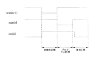
まず、初期化動作時には、図2に示されるように、以前スキャン信号scan[n−1]がロウレベルであり、現在スキャン信号scan[n]と発光信号emi[n]がハイレベルである初期化区間において、ロウレベルの以前スキャン信号scan[n−1]によりトランジスタT34がオンとなり、ハイレベルの現在スキャン信号scan[n]と現在発光信号emi[n]により他のトランジスタT31−T33とT35−T36がオフとなるので、図3に示されるような初期化パス(実線で図示)が形成される。したがって、コンデンサC31に格納されていたデータ信号、すなわち駆動トランジスタT31のゲート電圧は初期化される。 First, during the initialization operation, as shown in FIG. 2, initialization is performed such that the previous scan signal scan [n−1] is at the low level, and the current scan signal scan [n] and the light emission signal emi [n] are at the high level. In the interval, the transistor T34 is turned on by the low-level previous scan signal scan [n-1], and the other transistors T31-T33 and T35-T36 are turned on by the high-level current scan signal scan [n] and the current light emission signal emi [n]. Is turned off, so that an initialization path (shown by a solid line) as shown in FIG. 3 is formed. Therefore, the data signal stored in the capacitor C31, that is, the gate voltage of the drive transistor T31 is initialized.
次に、データプログラム動作時には、図2のように、以前スキャン信号scan[n−1]がハイレベルであり、現在スキャン信号scan[n]がロウレベルであり、現在発光信号emi[n]がハイレベルであるプログラム区間において、トランジスタT34はオフとなり、ロウレベルの現在スキャン信号scan[n]によりトランジスタ(第3のトランジスタ)T33がオンとなり、駆動トランジスタT31はダイオード形態で接続される。 Next, during the data program operation, as shown in FIG. 2, the previous scan signal scan [n−1] is at the high level, the current scan signal scan [n] is at the low level, and the current emission signal emi [n] is at the high level. In the program section that is level, the transistor T34 is turned off, the transistor (third transistor) T33 is turned on by the current scan signal scan [n] at low level, and the drive transistor T31 is connected in a diode form.
この際、現在スキャン信号scan[n]によりスイッチングトランジスタT32もオンとなり、現在発光信号emi[n]によりスイッチングトランジスタT35、T36がオフとなるので、図4に実線で示されるようなデータプログラムパスが形成される。したがって、該当するデータラインに印加されるデータ電圧VDATAmがスレショルド電圧補償用トランジスタT33を介して前記駆動トランジスタT31のゲートに提供される。 At this time, the switching transistor T32 is also turned on by the current scan signal scan [n], and the switching transistors T35 and T36 are turned off by the current light emission signal emi [n]. Therefore, a data program path as shown by a solid line in FIG. It is formed. Accordingly, the data voltage VDATAm applied to the corresponding data line is provided to the gate of the driving transistor T31 through the threshold voltage compensation transistor T33.
前記駆動トランジスタT31は、ダイオード形態で接続されているので、トランジスタT31のゲート電圧にはVDATAm−VTH(T31)が印加され、前記ゲート電圧がコンデンサC31に格納されてプログラム動作が完了する。 Since the driving transistor T31 is connected in the form of a diode, VDATAm-VTH (T31) is applied to the gate voltage of the transistor T31, and the gate voltage is stored in the capacitor C31 to complete the program operation.
最後に、発光時には、図2に示されたように、以前スキャン信号scan[n−1]がハイレベルであり、現在スキャン信号scan[n]がハイレベルになってから、現在発光信号emi[n]がロウレベルとなる発光区間において、図5に実線で示されたような発光パスが形成される。すなわちロウレベルの現在発光信号emi[n]によりスイッチングトランジスタT35、T36がオンとなり、ハイレベルの以前スキャン信号scan[n−1]により初期化トランジスタT34がオフとなり、ハイレベルの現在スキャン信号scan[n]によりスレショルド電圧補償用トランジスタT33とスイッチングトランジスタT32がオフとなる。したがって、駆動トランジスタT31のゲートに印加される電圧レベルのデータ信号に対応して発生する駆動電流がトランジスタT31を介して有機EL素子EL31に提供されることによって、有機EL素子EL31は発光することになる。 Finally, at the time of light emission, as shown in FIG. 2, the current scan signal scan [n−1] is at a high level and the current scan signal scan [n] is at a high level before the current light emission signal emi [ In the light emission section where n] is at a low level, a light emission path as shown by a solid line in FIG. 5 is formed. That is, the switching transistors T35 and T36 are turned on by the low level current emission signal emi [n], the initialization transistor T34 is turned off by the high level previous scan signal scan [n−1], and the high level current scan signal scan [n]. ], The threshold voltage compensating transistor T33 and the switching transistor T32 are turned off. Accordingly, the organic EL element EL31 emits light when a drive current generated in response to the voltage level data signal applied to the gate of the drive transistor T31 is provided to the organic EL element EL31 via the transistor T31. Become.
この際、有機EL素子EL31に流れる電流は、下記数2で表される。
上記数2中、IEL31は有機EL素子EL31に流れる電流、VGSはトランジスタT31のソースとゲート間の電圧、VTH(T31)はトランジスタT31のスレショルド電圧、VDATAはデータ電圧、βは定数値を各々示す。 In Equation 2, I EL31 is a current flowing through the organic EL element EL31, V GS is a voltage between the source and gate of the transistor T31, V TH (T31) is a threshold voltage of the transistor T31, V DATA is a data voltage, and β is a constant voltage. Each numerical value is shown.
上記数2から分かるように、電流駆動用トランジスタT31のスレショルド電圧に関係なくデータラインに印加される電圧レベルのデータ信号に対応して駆動電流がEL素子EL31を介して流れる。すなわち本発明では、電流駆動用トランジスタT31のスレショルド電圧の変動をトランジスタT33を介して検出し、自ら補償するため、有機EL素子に流れる電流を微細に制御でき、これにより、高い階調の有機EL装置を提供できる。 As can be seen from Equation 2, a drive current flows through the EL element EL31 in accordance with the voltage level data signal applied to the data line regardless of the threshold voltage of the current drive transistor T31. That is, in the present invention, the fluctuation of the threshold voltage of the current driving transistor T31 is detected via the transistor T33 and compensated for itself, so that the current flowing through the organic EL element can be finely controlled. Equipment can be provided.
また、以前フレーム時間のデータが高いレベルであり、次のフレーム時間のデータが低いレベルの電圧ならば、トランジスタT31のダイオード接続特性によりトランジスタT31のゲートノードには、これ以上データ信号が印加されることができないので、スイッチングトランジスタT34を設けることによって、トランジスタT31のゲートノードをフレーム毎に所定のレベルVintiに初期化させる。 If the data of the previous frame time is at a high level and the data of the next frame time is at a low level, a data signal is applied to the gate node of the transistor T31 due to the diode connection characteristics of the transistor T31. Since the switching transistor T34 is provided, the gate node of the transistor T31 is initialized to a predetermined level Vinti for each frame.
上述したように、本発明では、駆動トランジスタT31が自分のスレショルド電圧を検出して(self-Vth detection)、スレショルド電圧の変動を自ら補償できる。 As described above, in the present invention, the drive transistor T31 can detect its own threshold voltage (self-Vth detection) and compensate for the fluctuation of the threshold voltage by itself.
本発明の実施形態では、画素回路が6つのトランジスタと1つのコンデンサとで構成されるものを例示したが、スレショルド電圧を検出して自ら補償する構造には、いずれのものにも適用可能である。また、PMOSトランジスタの他にNMOSトランジスタまたはCMOSトランジスタなどで構成することも可能である。 In the embodiment of the present invention, the pixel circuit is configured by six transistors and one capacitor. However, the present invention can be applied to any structure that detects the threshold voltage and compensates itself. . In addition to the PMOS transistor, an NMOS transistor or a CMOS transistor can also be used.
本発明は、本発明の技術的思想から逸脱することなく、他の種々の形態で実施することができる。前述の実施形態は、あくまでも、本発明の技術内容を明らかにするものであって、そのような具体例のみに限定して狭義に解釈されるべきものではなく、本発明の精神と特許請求の範囲内で、いろいろと変更して実施することができるものである。 The present invention can be implemented in various other forms without departing from the technical idea of the present invention. The above-described embodiments are merely to clarify the technical contents of the present invention, and should not be construed in a narrow sense as being limited to such specific examples. It can be implemented with various changes within the range.
T31 駆動トランジスタ
T32、T35、T36 スイッチングトランジスタ
T33 スレショルド電圧補償用トランジスタ
T34 初期化用のトランジスタ
C31 コンデンサ
EL31 有機電界発光素子
T31 Drive transistor T32, T35, T36 Switching transistor T33 Threshold voltage compensation transistor T34 Initialization transistor C31 Capacitor EL31 Organic electroluminescence device
Claims (16)
前記第1のトランジスタを介して伝達される電圧レベルのデータ信号によって駆動電流を発生する第2のトランジスタと、
前記第2のトランジスタのスレショルド電圧の変動を検出して補償するための第3のトランジスタと、
現在発光信号に応答して、電源電圧を前記第2のトランジスタのソースに提供するための第5のトランジスタと、
前記現在発光信号に応答して、前記第2のトランジスタを介してEL素子に駆動電流を提供する第6のトランジスタと、
前記第2のトランジスタのゲートに印加される電圧を格納するためのコンデンサと、
前記第2のトランジスタを介して発生する駆動電流に対応して発光するEL素子とを備えることを特徴とする有機電界発光表示装置の画素回路。 A first transistor for transmitting a voltage level data signal to a source of the second transistor in response to a current scanline signal;
A second transistor that generates a drive current according to a voltage level data signal transmitted through the first transistor;
A third transistor for detecting and compensating for variations in the threshold voltage of the second transistor;
A fifth transistor for providing a power supply voltage to a source of the second transistor in response to a current emission signal;
A sixth transistor for providing a driving current to an EL element through the second transistor in response to the current emission signal;
A capacitor for storing a voltage applied to the gate of the second transistor;
A pixel circuit of an organic light emitting display device, comprising: an EL element that emits light in response to a driving current generated through the second transistor.
データ書込みの時、電圧レベルのデータ信号がコンデンサに伝達されて保存され、発光時、前記コンデンサに保存された電圧に応答して駆動電流を発生する第2のトランジスタと、
データ書込みの時、前記現在スキャンライン信号に応答して電圧レベルのデータ信号に対応する電圧を前記第2のトランジスタのゲートに提供するための第3のトランジスタと、
データ書込みの時、前記第2のトランジスタのゲートに印加される電圧を格納するためのコンデンサと、
発光時、電源電圧を前記第2のトランジスタのソースに伝達するための第4のトランジスタと、
発光時、電圧レベルのデータ信号によって前記第2のトランジスタから提供される駆動電流を伝達する第5のトランジスタと、
前記第5のトランジスタを介して伝達される駆動電流に対応して発光するEL素子と、
初期化時、前記現在スキャンライン信号の直前のスキャンライン信号に応答して前記コンデンサに格納された電圧を放電させる初期化用の第6のトランジスタとを備え、
データ書込みの時、前記第3のトランジスタは、前記現在スキャンライン信号に応答して前記第2のトランジスタをダイオード形態で接続させることによって、前記第2のトランジスタのスレショルド電圧の変動を検出して補償することを特徴とする有機電界発光表示装置の画素回路。 A first transistor for transmitting a voltage level data signal to a source of a second transistor in response to a current scan line signal when writing data;
A second transistor for generating a drive current in response to the voltage stored in the capacitor during light emission, and a voltage level data signal transmitted to the capacitor and stored;
A third transistor for providing a voltage corresponding to a data signal at a voltage level to the gate of the second transistor in response to the current scan line signal when writing data;
A capacitor for storing a voltage applied to the gate of the second transistor when writing data;
A fourth transistor for transmitting a power supply voltage to the source of the second transistor during light emission;
A fifth transistor for transmitting a driving current provided from the second transistor according to a voltage level data signal when emitting light;
An EL element that emits light in response to a drive current transmitted through the fifth transistor ;
A sixth transistor for initialization that discharges the voltage stored in the capacitor in response to a scan line signal immediately before the current scan line signal at the time of initialization ;
When data is written, the third transistor detects and compensates for a change in the threshold voltage of the second transistor by connecting the second transistor in a diode form in response to the current scan line signal. A pixel circuit of an organic light emitting display device.
前記第5のトランジスタは、前記現在発光信号がゲートに印加され、ソースが前記第2のトランジスタのドレインに接続され、ドレインが前記EL素子に接続されるPMOSトランジスタで構成されることを特徴とする請求項6に記載の有機電界発光表示装置の画素回路。 The fourth transistor is a PMOS transistor in which a current emission signal is applied to the gate, a power supply voltage is applied to the source, and a drain is connected to the source of the second transistor,
The fifth transistor includes a PMOS transistor in which the current light emission signal is applied to a gate, a source is connected to a drain of the second transistor, and a drain is connected to the EL element. The pixel circuit of the organic light emitting display according to claim 6.
現在スキャンライン信号に応答して電圧レベルのデータ信号を第2のトランジスタのソースに伝達する第1のトランジスタと、
前記電圧レベルのデータ信号に応答して、前記EL素子を駆動させる駆動電流を発生するための第2のトランジスタと、
前記現在スキャンライン信号に応答して、前記第2のトランジスタをダイオード形態で接続させてそのスレショルド電圧を補償するための第3のトランジスタと、
前記第2のトランジスタのゲートに印加される電圧を格納するためのコンデンサと、
現在発光信号に応答して、電源電圧を前記第2のトランジスタのソースに伝達するための第4のトランジスタと、
前記現在発光信号に応答して、前記第2のトランジスタから提供される駆動電流を前記EL素子に提供するための第5のトランジスタとを備えることを特徴とする有機電界発光表示装置の画素回路。 An EL element that emits light by an applied drive current;
A first transistor for transmitting a voltage level data signal to a source of a second transistor in response to a current scanline signal;
A second transistor for generating a drive current for driving the EL element in response to the voltage level data signal;
In response to the current scanline signal, a third transistor for connecting the second transistor in diode form to compensate for its threshold voltage;
A capacitor for storing a voltage applied to the gate of the second transistor;
A fourth transistor for transmitting a power supply voltage to a source of the second transistor in response to a current emission signal;
And a fifth transistor for providing the EL element with a driving current provided from the second transistor in response to the current light emission signal.
前記第1のトランジスタのドレインにソースが接続される第2のトランジスタと、
前記第2のトランジスタのゲートとドレインに各々ドレインとソースが接続される第3のトランジスタと、
現在発光信号がゲートに印加され、ソースに電源電圧が印加され、ドレインが前記第2のトランジスタのソースに接続される第4のトランジスタと、
前記現在発光信号がゲートに印加され、ソースが前記第2のトランジスタのドレインに接続され、ドレインがEL素子の一方の端子に接続される第5のトランジスタと、
前記第5のトランジスタのドレインに一方の端子が接続され、他方の端子が接地されるEL素子と、
前記第2のトランジスタのゲートに一方の端子が接続され、他方の端子に前記電源電圧が印加されるコンデンサとを備えることを特徴とする有機電界発光表示装置の画素回路。 A first transistor having a scan line signal applied to the gate and a voltage level data signal applied to the source;
A second transistor having a source connected to the drain of the first transistor;
A third transistor having a drain and a source connected to the gate and drain of the second transistor,
A fourth transistor in which a current emission signal is applied to the gate, a power supply voltage is applied to the source, and a drain is connected to the source of the second transistor;
A fifth transistor in which the current emission signal is applied to a gate, a source is connected to a drain of the second transistor, and a drain is connected to one terminal of an EL element;
An EL element having one terminal connected to the drain of the fifth transistor and the other terminal grounded;
A pixel circuit of an organic light emitting display device, comprising: a capacitor having one terminal connected to the gate of the second transistor and the power supply voltage applied to the other terminal.
複数のスキャンラインと、
複数の電源ラインと、
前記複数のデータライン、スキャンライン及び電源ラインのうち該当する1つのデータライン、スキャンライン及び電源ラインに各々接続される複数の画素とを備える有機電界発光表示装置の画素回路であって、
各画素は、
ゲートに前記該当するスキャンラインに印加された現在スキャンライン信号が印加され、ソースに前記データラインから電圧レベルのデータ信号が印加される第1のトランジスタと、
前記第1のトランジスタのドレインにソースが接続される第2のトランジスタと、
前記第2のトランジスタのゲートとドレインに各々ドレインとソースが接続される第3のトランジスタと、
現在発光信号がゲートに印加され、ソースに前記電源ラインから電源電圧が印加され、ドレインが前記第2のトランジスタのソースに接続される第4のトランジスタと、
前記現在発光信号がゲートに印加され、ソースに前記第2のトランジスタのドレインが接続される第5のトランジスタと、
前記第5のトランジスタのドレインに一方の端子が接続され、他方の端子が接地された発光素子と、
前記第2のトランジスタのゲートに一方の端子が接続され、他方の端子に前記電源ラインから電源電圧が印加されるコンデンサとを備えることを特徴とする有機電界発光表示装置の画素回路。 Multiple data lines,
Multiple scanlines,
Multiple power lines,
A pixel circuit of an organic light emitting display device comprising a plurality of pixels connected to one corresponding data line, scan line, and power line among the plurality of data lines, scan line, and power line,
Each pixel is
A first transistor in which a current scan line signal applied to the corresponding scan line is applied to a gate and a voltage level data signal is applied to the source from the data line;
A second transistor having a source connected to the drain of the first transistor;
A third transistor having a drain and a source connected to the gate and drain of the second transistor,
A fourth transistor in which a current emission signal is applied to the gate, a power supply voltage is applied to the source from the power supply line, and a drain is connected to the source of the second transistor;
A fifth transistor in which the current emission signal is applied to the gate and the source of the drain of the second transistor is connected;
A light-emitting element having one terminal connected to the drain of the fifth transistor and the other terminal grounded;
A pixel circuit of an organic light emitting display device, comprising: a capacitor having one terminal connected to a gate of the second transistor and a power supply voltage applied to the other terminal from the power supply line.
複数のスキャンラインと、
複数の電源ラインと、
前記複数のデータライン、スキャンライン及び電源ラインのうち該当する1つのデータライン、スキャンライン及び電源ラインに各々接続される複数の画素とを備える有機電界発光表示装置の画素駆動方法であって、
前記方法は、
該当するスキャンラインの直前のスキャンラインに印加されるスキャンライン信号に応答して前記画素内に備えられたコンデンサに格納されていた電圧レベルのデータ信号に対応する電圧を初期化させる段階と、
該当するスキャンラインに印加されるスキャンライン信号に応答してEL素子を駆動するための駆動トランジスタのスレショルド電圧の変動を補償し、前記補償された電圧レベルのデータ信号を前記コンデンサに書込む段階と、
現在発光信号に応答して、前記電圧レベルのデータ信号に対応する駆動電流を発生し、EL素子を発光させる段階とを備えることを特徴とする有機電界発光表示装置の画素駆動方法。 Multiple data lines,
Multiple scanlines,
Multiple power lines,
A pixel driving method of an organic light emitting display comprising: a plurality of pixels connected to one corresponding data line, scan line, and power line among the plurality of data lines, scan line, and power line;
The method
Initializing a voltage corresponding to a data signal of a voltage level stored in a capacitor provided in the pixel in response to a scan line signal applied to a scan line immediately before the corresponding scan line;
Compensating a variation in a threshold voltage of a driving transistor for driving an EL element in response to a scan line signal applied to the corresponding scan line, and writing the data signal of the compensated voltage level to the capacitor; ,
And a step of generating a driving current corresponding to the data signal of the voltage level in response to the current light emission signal to cause the EL element to emit light.
Applications Claiming Priority (1)
| Application Number | Priority Date | Filing Date | Title |
|---|---|---|---|
| KR1020030045610A KR100560780B1 (en) | 2003-07-07 | 2003-07-07 | Pixel circuit in OLED and Method for fabricating the same |
Publications (2)
| Publication Number | Publication Date |
|---|---|
| JP2005031630A JP2005031630A (en) | 2005-02-03 |
| JP4391857B2 true JP4391857B2 (en) | 2009-12-24 |
Family
ID=33448349
Family Applications (1)
| Application Number | Title | Priority Date | Filing Date |
|---|---|---|---|
| JP2004066129A Expired - Lifetime JP4391857B2 (en) | 2003-07-07 | 2004-03-09 | Pixel circuit of organic light emitting display and driving method thereof |
Country Status (5)
| Country | Link |
|---|---|
| US (1) | US7414599B2 (en) |
| EP (1) | EP1496495B1 (en) |
| JP (1) | JP4391857B2 (en) |
| KR (1) | KR100560780B1 (en) |
| CN (1) | CN100386794C (en) |
Cited By (1)
| Publication number | Priority date | Publication date | Assignee | Title |
|---|---|---|---|---|
| US9412299B2 (en) | 2013-09-02 | 2016-08-09 | Japan Display Inc. | Drive circuit, display device, and drive method |
Families Citing this family (302)
| Publication number | Priority date | Publication date | Assignee | Title |
|---|---|---|---|---|
| KR100637433B1 (en) | 2004-05-24 | 2006-10-20 | 삼성에스디아이 주식회사 | Light emitting display |
| JP2000031880A (en) * | 1998-07-16 | 2000-01-28 | Kokusai Electric Co Ltd | Radio repeater |
| CA2555286A1 (en) * | 2004-02-09 | 2005-08-25 | Bunn-O-Matic Corporation | Apparatus, system and method for infusing a pre-packaged pod |
| GB2411758A (en) * | 2004-03-04 | 2005-09-07 | Seiko Epson Corp | Pixel circuit |
| KR100560446B1 (en) | 2004-03-15 | 2006-03-13 | 삼성에스디아이 주식회사 | Light emitting display and driving method thereof |
| KR100560445B1 (en) * | 2004-03-15 | 2006-03-13 | 삼성에스디아이 주식회사 | Light emitting display and driving method thereof |
| KR101142994B1 (en) * | 2004-05-20 | 2012-05-08 | 삼성전자주식회사 | Display device and driving method thereof |
| KR100658616B1 (en) | 2004-05-31 | 2006-12-15 | 삼성에스디아이 주식회사 | Light emitting display device and display panel and driving method thereof |
| TW200620207A (en) * | 2004-07-05 | 2006-06-16 | Sony Corp | Pixel circuit, display device, driving method of pixel circuit, and driving method of display device |
| KR100592641B1 (en) * | 2004-07-28 | 2006-06-26 | 삼성에스디아이 주식회사 | Pixel circuit and organic light emitting display using the same |
| KR100673759B1 (en) * | 2004-08-30 | 2007-01-24 | 삼성에스디아이 주식회사 | Light emitting display |
| JP4160032B2 (en) | 2004-09-01 | 2008-10-01 | シャープ株式会社 | Display device and driving method thereof |
| KR100612392B1 (en) | 2004-10-13 | 2006-08-16 | 삼성에스디아이 주식회사 | Light emitting display and light emitting display panel |
| KR100606416B1 (en) * | 2004-11-17 | 2006-07-31 | 엘지.필립스 엘시디 주식회사 | Driving Apparatus And Method For Organic Light-Emitting Diode |
| KR100739318B1 (en) * | 2004-11-22 | 2007-07-12 | 삼성에스디아이 주식회사 | Pixel circuit and light emitting display |
| KR100688802B1 (en) * | 2004-11-22 | 2007-03-02 | 삼성에스디아이 주식회사 | Pixel and light emitting display |
| JP4364849B2 (en) * | 2004-11-22 | 2009-11-18 | 三星モバイルディスプレイ株式會社 | Luminescent display device |
| KR100688801B1 (en) | 2004-11-22 | 2007-03-02 | 삼성에스디아이 주식회사 | Delta pixel circuit and light emitting display |
| KR100604061B1 (en) * | 2004-12-09 | 2006-07-24 | 삼성에스디아이 주식회사 | Pixel circuit and light emitting display |
| KR100602363B1 (en) * | 2005-01-10 | 2006-07-18 | 삼성에스디아이 주식회사 | Emission driver and light emitting display for using the same |
| CN1822385B (en) | 2005-01-31 | 2013-02-06 | 株式会社半导体能源研究所 | Display device and electronic device comprising same |
| KR100642264B1 (en) * | 2005-02-04 | 2006-11-06 | 재단법인서울대학교산학협력재단 | Picture element structure of organic light emitting diode |
| KR101152120B1 (en) * | 2005-03-16 | 2012-06-15 | 삼성전자주식회사 | Display device and driving method thereof |
| KR100653846B1 (en) * | 2005-04-11 | 2006-12-05 | 실리콘 디스플레이 (주) | circuit and method for driving 0rganic Light-Emitting Diode |
| JP5392963B2 (en) * | 2005-04-19 | 2014-01-22 | インテレクチュアル キーストーン テクノロジー エルエルシー | Electro-optical device and electronic apparatus |
| KR100840116B1 (en) * | 2005-04-28 | 2008-06-20 | 삼성에스디아이 주식회사 | Light Emitting Diode Display |
| KR100731743B1 (en) * | 2005-04-29 | 2007-06-22 | 삼성에스디아이 주식회사 | Pixel Circuit of Organic Electoluminescent Display Device |
| US7872620B2 (en) * | 2005-04-29 | 2011-01-18 | Seoul National University Industry Foundation | Pixel structure using voltage programming-type for active matrix organic light emitting device |
| KR100719924B1 (en) * | 2005-04-29 | 2007-05-18 | 비오이 하이디스 테크놀로지 주식회사 | Organic electroluminescence display device |
| KR100782455B1 (en) * | 2005-04-29 | 2007-12-05 | 삼성에스디아이 주식회사 | Emission Control Driver and Organic Electro Luminescence Display Device of having the same |
| KR100683772B1 (en) * | 2005-05-13 | 2007-02-15 | 삼성에스디아이 주식회사 | Organic light emitting display device |
| KR100624314B1 (en) | 2005-06-22 | 2006-09-19 | 삼성에스디아이 주식회사 | Light emission display device and thin film transistor |
| TW200707385A (en) * | 2005-07-15 | 2007-02-16 | Seiko Epson Corp | Electronic device, method of driving the same, electro-optical device, and electronic apparatus |
| KR100547515B1 (en) * | 2005-07-27 | 2006-01-31 | 실리콘 디스플레이 (주) | Organic light emitting diode display and method for driving oled |
| KR100635509B1 (en) * | 2005-08-16 | 2006-10-17 | 삼성에스디아이 주식회사 | Organic electroluminescent display device |
| KR100636502B1 (en) * | 2005-08-31 | 2006-10-18 | 삼성에스디아이 주식회사 | Organic electro luminescence display for performing sheet unit test and testing method using the same |
| KR100666640B1 (en) * | 2005-09-15 | 2007-01-09 | 삼성에스디아이 주식회사 | Organic electroluminescent display device |
| EP1764770A3 (en) | 2005-09-16 | 2012-03-14 | Semiconductor Energy Laboratory Co., Ltd. | Display device and driving method of display device |
| JP5057731B2 (en) * | 2005-09-16 | 2012-10-24 | 株式会社半導体エネルギー研究所 | Display device, module, and electronic device |
| JP4923505B2 (en) | 2005-10-07 | 2012-04-25 | ソニー株式会社 | Pixel circuit and display device |
| KR100662998B1 (en) * | 2005-11-04 | 2006-12-28 | 삼성에스디아이 주식회사 | Organic light emitting display and driving method thereof |
| KR100732828B1 (en) * | 2005-11-09 | 2007-06-27 | 삼성에스디아이 주식회사 | Pixel and Organic Light Emitting Display Using the same |
| JP5160748B2 (en) | 2005-11-09 | 2013-03-13 | 三星ディスプレイ株式會社 | Luminescent display device |
| CN101313348B (en) * | 2005-12-02 | 2011-07-06 | 株式会社半导体能源研究所 | Semiconductor device, display device, and electronic device |
| KR100754140B1 (en) | 2005-12-21 | 2007-08-31 | 삼성에스디아이 주식회사 | Organic Light Emitting Display and Mother Substrate for Performing Sheet Unit Test and Testing Method Using the Same |
| TWI279763B (en) * | 2006-03-13 | 2007-04-21 | Himax Tech Ltd | Light emitting display, pixel circuit and driving method thereof |
| KR100698703B1 (en) * | 2006-03-28 | 2007-03-23 | 삼성에스디아이 주식회사 | Pixel and Organic Light Emitting Display Using the Pixel |
| KR100784014B1 (en) | 2006-04-17 | 2007-12-07 | 삼성에스디아이 주식회사 | Organic Light Emitting Display Device and Driving Method Thereof |
| TWI371018B (en) * | 2006-05-09 | 2012-08-21 | Chimei Innolux Corp | System for displaying image and driving display element method |
| KR100793557B1 (en) | 2006-06-05 | 2008-01-14 | 삼성에스디아이 주식회사 | Organic electro luminescence display and driving method thereof |
| JP2007323036A (en) * | 2006-06-05 | 2007-12-13 | Samsung Sdi Co Ltd | Organic electroluminescence display and driving method thereof |
| KR100810602B1 (en) * | 2006-06-05 | 2008-03-06 | 재단법인서울대학교산학협력재단 | Picture element structure of voltage programming method type |
| KR100740133B1 (en) * | 2006-07-31 | 2007-07-16 | 삼성에스디아이 주식회사 | Light emitting display |
| KR100739335B1 (en) * | 2006-08-08 | 2007-07-12 | 삼성에스디아이 주식회사 | Pixel and organic light emitting display device using the same |
| JP2008046377A (en) * | 2006-08-17 | 2008-02-28 | Sony Corp | Display device |
| TWI340370B (en) * | 2006-08-24 | 2011-04-11 | Chimei Innolux Corp | System for displaying image |
| TWI326066B (en) * | 2006-09-22 | 2010-06-11 | Au Optronics Corp | Organic light emitting diode display and related pixel circuit |
| CN100437708C (en) * | 2006-09-22 | 2008-11-26 | 北京交通大学 | Pixel drive circuit of active organic electroluminescent display device |
| CN100435199C (en) * | 2006-11-03 | 2008-11-19 | 友达光电股份有限公司 | Organic illuminating display and relative pixel circuit |
| JP4887203B2 (en) | 2006-11-14 | 2012-02-29 | 三星モバイルディスプレイ株式會社 | Pixel, organic electroluminescent display device, and driving method of organic electroluminescent display device |
| KR100846948B1 (en) * | 2006-12-13 | 2008-07-17 | 삼성에스디아이 주식회사 | Organic Light Emitting Display |
| US7782278B2 (en) * | 2006-12-14 | 2010-08-24 | Himax Technologies Limited | Intra-pixel convolution for AMOLED |
| JP2008151963A (en) * | 2006-12-15 | 2008-07-03 | Semiconductor Energy Lab Co Ltd | Semiconductor device and method of driving the same |
| KR100824852B1 (en) * | 2006-12-20 | 2008-04-23 | 삼성에스디아이 주식회사 | Organic light emitting display |
| KR100833753B1 (en) * | 2006-12-21 | 2008-05-30 | 삼성에스디아이 주식회사 | Organic light emitting diode display and driving method thereof |
| KR101373736B1 (en) | 2006-12-27 | 2014-03-14 | 삼성디스플레이 주식회사 | Display device and driving method thereof |
| CN100998941B (en) * | 2007-01-04 | 2012-09-05 | 华东理工大学 | Precatalyst and its preparation method |
| JP5008412B2 (en) | 2007-02-01 | 2012-08-22 | エルジー ディスプレイ カンパニー リミテッド | Image display device and driving method of image display device |
| KR100836430B1 (en) * | 2007-02-05 | 2008-06-09 | 삼성에스디아이 주식회사 | Organic light emitting display device |
| KR100865394B1 (en) | 2007-03-02 | 2008-10-24 | 삼성에스디아이 주식회사 | Organic Light Emitting Display |
| KR100873074B1 (en) * | 2007-03-02 | 2008-12-09 | 삼성모바일디스플레이주식회사 | Pixel, Organic Light Emitting Display Device and Driving Method Thereof |
| US7911459B2 (en) * | 2007-03-28 | 2011-03-22 | Himax Technologies Limited | Pixel circuit |
| US7920110B2 (en) * | 2007-03-28 | 2011-04-05 | Himax Technologies Limited | Pixel circuit |
| KR100807062B1 (en) * | 2007-04-06 | 2008-02-25 | 삼성에스디아이 주식회사 | Organic light emitting display |
| KR100873078B1 (en) * | 2007-04-10 | 2008-12-09 | 삼성모바일디스플레이주식회사 | Pixel, Organic Light Emitting Display Device and Driving Method Thereof |
| KR100858618B1 (en) * | 2007-04-10 | 2008-09-17 | 삼성에스디아이 주식회사 | Organic light emitting display and driving method thereof |
| KR101526475B1 (en) | 2007-06-29 | 2015-06-05 | 가부시키가이샤 한도오따이 에네루기 켄큐쇼 | Display device and driving method thereof |
| KR100893482B1 (en) * | 2007-08-23 | 2009-04-17 | 삼성모바일디스플레이주식회사 | Organic Light Emitting Display and Driving Method Thereof |
| KR100911976B1 (en) * | 2007-11-23 | 2009-08-13 | 삼성모바일디스플레이주식회사 | Organic Light Emitting Display Device |
| JP5115180B2 (en) * | 2007-12-21 | 2013-01-09 | ソニー株式会社 | Self-luminous display device and driving method thereof |
| KR101407302B1 (en) * | 2007-12-27 | 2014-06-13 | 엘지디스플레이 주식회사 | Luminescence dispaly and driving method thereof |
| KR100902238B1 (en) * | 2008-01-18 | 2009-06-11 | 삼성모바일디스플레이주식회사 | Organic light emitting display and driving method thereof |
| JP2009276744A (en) * | 2008-02-13 | 2009-11-26 | Toshiba Mobile Display Co Ltd | El display device |
| KR101361981B1 (en) * | 2008-02-19 | 2014-02-21 | 엘지디스플레이 주식회사 | Organic Light Emitting Diode Display And Driving Method Thereof |
| JP2009211039A (en) * | 2008-03-04 | 2009-09-17 | Samsung Mobile Display Co Ltd | Organic light emitting display device |
| JP2009237558A (en) | 2008-03-05 | 2009-10-15 | Semiconductor Energy Lab Co Ltd | Driving method for semiconductor device |
| KR100922071B1 (en) | 2008-03-10 | 2009-10-16 | 삼성모바일디스플레이주식회사 | Pixel and Organic Light Emitting Display Using the same |
| KR20090106162A (en) * | 2008-04-04 | 2009-10-08 | 삼성모바일디스플레이주식회사 | Organic light emitting display apparatus and driving method thereof |
| JP2009271199A (en) * | 2008-05-01 | 2009-11-19 | Sony Corp | Display apparatus and driving method for display apparatus |
| JP2009271200A (en) | 2008-05-01 | 2009-11-19 | Sony Corp | Display apparatus and driving method for display apparatus |
| JP2009288767A (en) | 2008-05-01 | 2009-12-10 | Sony Corp | Display apparatus and driving method thereof |
| JP2009271333A (en) * | 2008-05-08 | 2009-11-19 | Toshiba Mobile Display Co Ltd | El display device |
| JP4816686B2 (en) | 2008-06-06 | 2011-11-16 | ソニー株式会社 | Scan driver circuit |
| JP2010002498A (en) * | 2008-06-18 | 2010-01-07 | Sony Corp | Panel and drive control method |
| JP4844598B2 (en) | 2008-07-14 | 2011-12-28 | ソニー株式会社 | Scan driver circuit |
| KR101282996B1 (en) | 2008-11-15 | 2013-07-04 | 엘지디스플레이 주식회사 | Organic electro-luminescent display device and driving method thereof |
| JP5736114B2 (en) | 2009-02-27 | 2015-06-17 | 株式会社半導体エネルギー研究所 | Semiconductor device driving method and electronic device driving method |
| US9047815B2 (en) | 2009-02-27 | 2015-06-02 | Semiconductor Energy Laboratory Co., Ltd. | Method for driving semiconductor device |
| JP5502864B2 (en) | 2009-07-01 | 2014-05-28 | シャープ株式会社 | Active matrix substrate and organic EL display device |
| US8786526B2 (en) | 2009-07-28 | 2014-07-22 | Sharp Kabushiki Kaisha | Active matrix substrate, display device, and organic EL display device |
| KR101082167B1 (en) * | 2009-09-07 | 2011-11-09 | 삼성모바일디스플레이주식회사 | Organic Light Emitting Display and Driving Method Thereof |
| KR101621329B1 (en) | 2009-09-30 | 2016-05-17 | 엘지디스플레이 주식회사 | Organic electroluminescent display device and method of driving the same |
| KR20110041107A (en) | 2009-10-15 | 2011-04-21 | 삼성모바일디스플레이주식회사 | Organic light emitting diode display device and fabrication method of the same |
| US8575602B2 (en) | 2009-10-20 | 2013-11-05 | Sharp Kabushiki Kaisha | Active matrix substrate and organic EL display device |
| KR101042956B1 (en) * | 2009-11-18 | 2011-06-20 | 삼성모바일디스플레이주식회사 | Pixel circuit and organic light emitting display using thereof |
| KR101064471B1 (en) * | 2010-03-17 | 2011-09-15 | 삼성모바일디스플레이주식회사 | Organic light emitting display device |
| KR101142644B1 (en) | 2010-03-17 | 2012-05-03 | 삼성모바일디스플레이주식회사 | Organic Light Emitting Display Device |
| KR101093374B1 (en) | 2010-05-10 | 2011-12-14 | 삼성모바일디스플레이주식회사 | Organic Light Emitting Display Device |
| KR101351416B1 (en) | 2010-05-18 | 2014-01-14 | 엘지디스플레이 주식회사 | Pixel circuit of voltage compensation type of active matrix organic light emitting diode display device |
| KR101162856B1 (en) * | 2010-06-01 | 2012-07-06 | 삼성모바일디스플레이주식회사 | Organic Light Emitting Display Device |
| TWI493524B (en) | 2010-06-10 | 2015-07-21 | Prime View Int Co Ltd | Pixel driver of light emitting display and associated method and apparatus |
| CN102280085B (en) * | 2010-06-10 | 2013-09-11 | 元太科技工业股份有限公司 | Pixel drive circuit and method and light-emitting display device |
| KR101152504B1 (en) | 2010-06-21 | 2012-06-01 | 삼성모바일디스플레이주식회사 | Pixel and Organic Light Emitting Display Device Using the same |
| KR101152580B1 (en) | 2010-06-30 | 2012-06-01 | 삼성모바일디스플레이주식회사 | Pixel and Organic Light Emitting Display Device Using the Same |
| KR101152466B1 (en) * | 2010-06-30 | 2012-06-01 | 삼성모바일디스플레이주식회사 | Pixel and Organic Light Emitting Display Device Using the Same |
| TWI406228B (en) * | 2010-07-08 | 2013-08-21 | Au Optronics Corp | Pixel structure and pixel structure of organic emitting device |
| KR101758771B1 (en) | 2010-07-20 | 2017-08-01 | 삼성디스플레이 주식회사 | Pixel and Organic Light Emitting Display Device Using the same |
| KR101682691B1 (en) | 2010-07-20 | 2016-12-07 | 삼성디스플레이 주식회사 | Pixel and Organic Light Emitting Display Device Using the same |
| KR101762344B1 (en) | 2010-07-27 | 2017-07-31 | 삼성디스플레이 주식회사 | Organic electroluminescence emitting display device |
| KR101791664B1 (en) | 2010-10-28 | 2017-11-21 | 삼성디스플레이 주식회사 | Organic Light Emitting Display Device |
| KR101748857B1 (en) | 2010-10-28 | 2017-06-20 | 삼성디스플레이 주식회사 | Organic Light Emitting Display Device |
| KR101768848B1 (en) | 2010-10-28 | 2017-08-18 | 삼성디스플레이 주식회사 | Organic electroluminescence emitting display device |
| KR101719567B1 (en) | 2010-10-28 | 2017-03-27 | 삼성디스플레이 주식회사 | Organic Light Emitting Display Device |
| KR20120044507A (en) | 2010-10-28 | 2012-05-08 | 삼성모바일디스플레이주식회사 | Organic light emitting display device and driving method thereof |
| KR101738920B1 (en) | 2010-10-28 | 2017-05-24 | 삼성디스플레이 주식회사 | Organic Light Emitting Display Device |
| KR101765778B1 (en) * | 2010-12-06 | 2017-08-08 | 삼성디스플레이 주식회사 | Organic Light Emitting Display Device |
| KR20120062252A (en) | 2010-12-06 | 2012-06-14 | 삼성모바일디스플레이주식회사 | Pixel and organic light emitting display device using the pixel |
| KR20120062251A (en) | 2010-12-06 | 2012-06-14 | 삼성모바일디스플레이주식회사 | Pixel and organic light emitting display device using the pixel |
| KR20120062499A (en) | 2010-12-06 | 2012-06-14 | 삼성모바일디스플레이주식회사 | Pixel, stereopsis display device and driving method thereof |
| KR20120065137A (en) * | 2010-12-10 | 2012-06-20 | 삼성모바일디스플레이주식회사 | Pixel, display device and driving method thereof |
| CN107301842A (en) * | 2017-08-17 | 2017-10-27 | 深圳市华星光电半导体显示技术有限公司 | A kind of OLED pixel drive circuit and image element driving method |
| CN102708786B (en) * | 2011-08-25 | 2014-12-10 | 京东方科技集团股份有限公司 | Active matrix organic light emitting diode (AMOLED) pixel unit driving circuit and method, pixel unit and display device |
| CN102708787A (en) * | 2011-08-25 | 2012-10-03 | 京东方科技集团股份有限公司 | Active matrix organic light emitting diode (AMOLED) pixel unit driving circuit and method, pixel unit and display device |
| TWI471842B (en) * | 2011-10-05 | 2015-02-01 | Wintek Corp | Control circuit for orginic light emitting diode pixel |
| TW201316315A (en) * | 2011-10-05 | 2013-04-16 | Wintek Corp | Light-emitting component driving circuit and related pixel circuit and applications using the same |
| CN103050080B (en) * | 2011-10-11 | 2015-08-12 | 上海天马微电子有限公司 | The image element circuit of organic light emitting display and driving method thereof |
| CN102654975B (en) * | 2011-11-01 | 2014-08-20 | 京东方科技集团股份有限公司 | AMOLED (active matrix/organic light emitting diode) drive compensation circuit and method and display device thereof |
| WO2013065595A1 (en) * | 2011-11-02 | 2013-05-10 | シャープ株式会社 | Pixel circuit, display device provided therewith, and pixel circuit control method |
| WO2013065594A1 (en) * | 2011-11-02 | 2013-05-10 | シャープ株式会社 | Color display device |
| WO2013065596A1 (en) * | 2011-11-02 | 2013-05-10 | シャープ株式会社 | Pixel circuit, display device provided therewith, and pixel circuit control method |
| WO2013069560A1 (en) * | 2011-11-10 | 2013-05-16 | シャープ株式会社 | Display device and drive method for same |
| CN102708791B (en) * | 2011-12-01 | 2014-05-14 | 京东方科技集团股份有限公司 | Pixel unit driving circuit and method, pixel unit and display device |
| CN202422687U (en) * | 2012-01-04 | 2012-09-05 | 京东方科技集团股份有限公司 | Pixel unit driving circuit, pixel unit and display device |
| CN102708798B (en) * | 2012-04-28 | 2015-05-13 | 京东方科技集团股份有限公司 | Pixel unit driving circuit, driving method, pixel unit and display device |
| KR101911489B1 (en) * | 2012-05-29 | 2018-10-26 | 삼성디스플레이 주식회사 | Organic Light Emitting Display Device with Pixel and Driving Method Thereof |
| KR101905793B1 (en) | 2012-06-04 | 2018-10-11 | 삼성디스플레이 주식회사 | Organic Light Emitting Display integrated Touch Screen Panel |
| CN104380368B (en) | 2012-07-31 | 2016-08-24 | 夏普株式会社 | Display device and driving method thereof |
| US9633599B2 (en) | 2012-07-31 | 2017-04-25 | Sharp Kabushiki Kaisha | Pixel circuit, display device including the same and driving method of the display device |
| WO2014021150A1 (en) | 2012-07-31 | 2014-02-06 | シャープ株式会社 | Display device and driving method therefor |
| US9305492B2 (en) | 2012-08-02 | 2016-04-05 | Sharp Kabushiki Kaisha | Display device and method for driving the same |
| KR20140028921A (en) | 2012-08-31 | 2014-03-10 | 삼성디스플레이 주식회사 | Pixel and organic light emitting display device using the same |
| KR101999759B1 (en) * | 2012-09-11 | 2019-07-16 | 삼성디스플레이 주식회사 | Organic Light Emitting Display Device and Driving Method Thereof |
| KR101975000B1 (en) * | 2012-09-13 | 2019-05-07 | 삼성디스플레이 주식회사 | Organic light emitting diode display |
| US9293080B2 (en) | 2012-09-19 | 2016-03-22 | Sharp Kabushiki Kaisha | Data line driving circuit, display device including same, and data line driving method |
| KR20140050361A (en) | 2012-10-19 | 2014-04-29 | 삼성디스플레이 주식회사 | Pixel, stereopsis display device and driving method thereof |
| CN103489399B (en) * | 2012-11-21 | 2015-09-02 | 友达光电股份有限公司 | Electroluminescent pixel circuit |
| CN103137069A (en) * | 2012-11-21 | 2013-06-05 | 友达光电股份有限公司 | Pixel circuit |
| JP2014109707A (en) | 2012-12-03 | 2014-06-12 | Samsung Display Co Ltd | Drive method of electro-optic device and electro-optic device |
| KR101987933B1 (en) * | 2012-12-13 | 2019-06-12 | 삼성디스플레이 주식회사 | Pixel and Organic Light Emitting Display Device Using the same |
| KR20140081262A (en) | 2012-12-21 | 2014-07-01 | 삼성디스플레이 주식회사 | Pixel and Organic Light Emitting Display Device |
| KR101411621B1 (en) * | 2012-12-24 | 2014-07-02 | 엘지디스플레이 주식회사 | Organic light emitting diode display device and method for driving the same |
| CN103021339B (en) * | 2012-12-31 | 2015-09-16 | 昆山工研院新型平板显示技术中心有限公司 | Image element circuit, display device and driving method thereof |
| KR102061108B1 (en) * | 2013-01-16 | 2020-01-02 | 삼성디스플레이 주식회사 | Organic Light Emitting Display integrated Touch Screen Panel |
| US9576535B2 (en) | 2013-01-17 | 2017-02-21 | Samsung Display Co., Ltd. | Pixel and organic light emitting display using the same |
| CN103137071A (en) * | 2013-03-04 | 2013-06-05 | 陈鑫 | Novel active pixel driving circuit with capacity for threshold value compensation |
| WO2014141958A1 (en) | 2013-03-14 | 2014-09-18 | シャープ株式会社 | Display device and method for driving same |
| KR20140120167A (en) * | 2013-04-02 | 2014-10-13 | 삼성디스플레이 주식회사 | Organic Light Emitting Display Having Repaired Pixel and Pixel Repairing Method Thereof |
| CN105144274B (en) | 2013-04-23 | 2017-07-11 | 夏普株式会社 | Display device and its driving current detection method |
| CN103236237B (en) * | 2013-04-26 | 2015-04-08 | 京东方科技集团股份有限公司 | Pixel unit circuit and compensating method of pixel unit circuit as well as display device |
| CN103226931B (en) * | 2013-04-27 | 2015-09-09 | 京东方科技集团股份有限公司 | Image element circuit and organic light emitting display |
| KR102077661B1 (en) * | 2013-05-07 | 2020-02-17 | 삼성디스플레이 주식회사 | Organic light emitting display device and driving method thereof |
| KR102003489B1 (en) | 2013-05-13 | 2019-07-25 | 삼성디스플레이 주식회사 | Pixel and Organic Light Emitting Display Device Using the same |
| KR20140140272A (en) | 2013-05-29 | 2014-12-09 | 삼성디스플레이 주식회사 | Pixel and Organic Light Emitting Display Device Using the same |
| KR20140140271A (en) | 2013-05-29 | 2014-12-09 | 삼성디스플레이 주식회사 | Pixel and Organic Light Emitting Display Device Using the same |
| KR20140142002A (en) | 2013-06-03 | 2014-12-11 | 삼성디스플레이 주식회사 | Display device and driving method thereof |
| TW201447848A (en) * | 2013-06-11 | 2014-12-16 | Au Optronics Corp | Displaying apparatus and driving method thereof |
| WO2014203810A1 (en) | 2013-06-20 | 2014-12-24 | シャープ株式会社 | Display device and method for driving same |
| US9837016B2 (en) | 2013-06-27 | 2017-12-05 | Sharp Kabushiki Kaisha | Display device and drive method therefor |
| CN105247603B (en) | 2013-06-27 | 2017-07-11 | 夏普株式会社 | Display device and its driving method |
| TWI494905B (en) * | 2013-07-01 | 2015-08-01 | Au Optronics Corp | Organic light-emitting diode display panel |
| JP6225511B2 (en) * | 2013-07-02 | 2017-11-08 | セイコーエプソン株式会社 | Display device and electronic device |
| CN103400548B (en) * | 2013-07-31 | 2016-03-16 | 京东方科技集团股份有限公司 | Pixel-driving circuit and driving method, display device |
| KR102097476B1 (en) * | 2013-08-12 | 2020-04-07 | 삼성디스플레이 주식회사 | Organic light emitting display device and method for driving the same |
| JP6562608B2 (en) | 2013-09-19 | 2019-08-21 | 株式会社半導体エネルギー研究所 | Electronic device and driving method of electronic device |
| CN103500556B (en) * | 2013-10-09 | 2015-12-02 | 京东方科技集团股份有限公司 | A kind of image element circuit and driving method, thin film transistor backplane |
| CN104658470A (en) * | 2013-11-22 | 2015-05-27 | 上海和辉光电有限公司 | Oled pixel circuit |
| US9647048B2 (en) | 2013-11-26 | 2017-05-09 | Apple Inc. | Capacitor structures for display pixel threshold voltage compensation circuits |
| CN104376813B (en) * | 2013-11-26 | 2017-09-08 | 苹果公司 | Display picture element unit |
| JP2015102793A (en) | 2013-11-27 | 2015-06-04 | 株式会社ジャパンディスプレイ | Display device and method for driving display device |
| US9842545B2 (en) | 2013-12-20 | 2017-12-12 | Sharp Kabushiki Kaisha | Display device and method for driving same |
| KR102111747B1 (en) * | 2014-02-25 | 2020-05-18 | 삼성디스플레이 주식회사 | Organic light emitting display device |
| CN103985360B (en) * | 2014-05-04 | 2016-04-27 | 深圳市华星光电技术有限公司 | The driving circuit of display panel and liquid crystal indicator |
| TWI515712B (en) * | 2014-05-28 | 2016-01-01 | 友達光電股份有限公司 | Pixel driving circuit |
| CN104050916B (en) * | 2014-06-04 | 2016-08-31 | 上海天马有机发光显示技术有限公司 | The pixel compensation circuit of a kind of OLED and method |
| CN104123911B (en) * | 2014-07-01 | 2016-05-04 | 京东方科技集团股份有限公司 | A kind of driving method, drive unit and organic elctroluminescent device |
| CN104134427B (en) * | 2014-08-06 | 2016-08-24 | 友达光电股份有限公司 | Image element circuit |
| TWI546794B (en) * | 2014-09-03 | 2016-08-21 | 友達光電股份有限公司 | Circuitry of organic light emitting diode |
| CN104318894B (en) * | 2014-09-30 | 2017-02-15 | 京东方科技集团股份有限公司 | Pixel circuit driving method |
| KR102274740B1 (en) | 2014-10-13 | 2021-07-08 | 삼성디스플레이 주식회사 | Display device |
| KR20160054140A (en) | 2014-11-05 | 2016-05-16 | 삼성디스플레이 주식회사 | Organic light emitting display device and driving method thereof |
| JP2016118672A (en) | 2014-12-22 | 2016-06-30 | 株式会社ジャパンディスプレイ | Display device and method of driving the same |
| CN104537983B (en) * | 2014-12-30 | 2017-03-15 | 合肥鑫晟光电科技有限公司 | Image element circuit and its driving method, display device |
| CN104637445B (en) * | 2015-02-03 | 2017-03-08 | 深圳市华星光电技术有限公司 | AMOLED pixel-driving circuit and image element driving method |
| KR102307500B1 (en) | 2015-03-20 | 2021-10-01 | 삼성디스플레이 주식회사 | Pixel Circuit for Display Apparatus and Display Apparatus including Thereof |
| CN106157882B (en) * | 2015-04-24 | 2019-01-15 | 上海和辉光电有限公司 | Dot structure |
| EP3098804A3 (en) * | 2015-05-28 | 2016-12-21 | LG Display Co., Ltd. | Organic light emitting display |
| CN104978931B (en) * | 2015-07-09 | 2017-11-21 | 上海天马有机发光显示技术有限公司 | Load device and method, display panel, the display of data voltage signal |
| KR102402605B1 (en) | 2015-07-28 | 2022-05-27 | 삼성디스플레이 주식회사 | organic light emitting display |
| CN105139805B (en) | 2015-10-19 | 2017-09-22 | 京东方科技集团股份有限公司 | A kind of pixel-driving circuit and its driving method, display device |
| JP2016042195A (en) * | 2015-11-12 | 2016-03-31 | 株式会社半導体エネルギー研究所 | Display device |
| CN106782328A (en) * | 2015-11-20 | 2017-05-31 | 上海和辉光电有限公司 | A kind of image element circuit |
| CN106887207A (en) * | 2015-12-15 | 2017-06-23 | 昆山工研院新型平板显示技术中心有限公司 | Image element circuit and its driving method and OLED |
| CN105609053B (en) * | 2015-12-31 | 2019-01-22 | 京东方科技集团股份有限公司 | driving device, driving method and display device |
| CN105427798B (en) * | 2016-01-05 | 2018-02-06 | 京东方科技集团股份有限公司 | A kind of image element circuit, display panel and display device |
| CN107180610B (en) * | 2016-03-11 | 2020-06-02 | 上海和辉光电有限公司 | Display panel and array substrate thereof |
| KR102493130B1 (en) | 2016-03-22 | 2023-01-31 | 삼성디스플레이 주식회사 | Pixel and organic light emitting display |
| JP2017187608A (en) | 2016-04-05 | 2017-10-12 | 株式会社ジャパンディスプレイ | Driving method for display device, and display device |
| US10482820B2 (en) | 2016-06-21 | 2019-11-19 | Novatek Microelectronics Corp. | Method of compensating luminance of OLED and display system using the same |
| US10388207B2 (en) | 2016-06-05 | 2019-08-20 | Novatek Microelectronics Corp. | External compensation method and driver IC using the same |
| KR102579142B1 (en) | 2016-06-17 | 2023-09-19 | 삼성디스플레이 주식회사 | Pixel and Organic Light Emitting Display Device and Driving Method Using the pixel |
| KR102559544B1 (en) | 2016-07-01 | 2023-07-26 | 삼성디스플레이 주식회사 | Display device |
| CN107689211B (en) | 2016-08-05 | 2022-05-13 | 天马微电子股份有限公司 | Display device |
| KR20180040185A (en) | 2016-10-11 | 2018-04-20 | 삼성디스플레이 주식회사 | Display device |
| KR102627074B1 (en) * | 2016-12-22 | 2024-01-22 | 엘지디스플레이 주식회사 | Display element, organic light emitting display device and data driver |
| CN106531075B (en) * | 2017-01-10 | 2019-01-22 | 上海天马有机发光显示技术有限公司 | Organic light emissive pixels driving circuit, driving method and organic light emitting display panel |
| CN108573675A (en) * | 2017-03-10 | 2018-09-25 | 昆山国显光电有限公司 | Display-apparatus driving method |
| KR102309599B1 (en) | 2017-04-11 | 2021-10-08 | 삼성디스플레이 주식회사 | Organic light emitting display device |
| US11328678B2 (en) | 2017-04-28 | 2022-05-10 | Shenzhen China Star Optoelectronics Semiconductor Display Technology Co., Ltd. | Display panel, pixel driving circuit, and drving method thereof |
| CN106910460B (en) * | 2017-04-28 | 2019-07-19 | 深圳市华星光电半导体显示技术有限公司 | Pixel-driving circuit and display panel |
| US10825399B2 (en) | 2018-01-12 | 2020-11-03 | Shenzhen China Star Optoelectronics Semiconductor Display Technology Co., Ltd. | Display panel, pixel driving circuit, and drying method thereof |
| CN106960659B (en) * | 2017-04-28 | 2019-09-27 | 深圳市华星光电半导体显示技术有限公司 | Display panel, pixel-driving circuit and its driving method |
| CN106887210B (en) * | 2017-04-28 | 2019-08-20 | 深圳市华星光电半导体显示技术有限公司 | Display panel, pixel-driving circuit and its driving method |
| US10204561B2 (en) * | 2017-07-06 | 2019-02-12 | Shenzhen China Star Optoelectronics Semiconductor Display Technology Co., Ltd. | Amoled pixel driving circuit and pixel driving method |
| KR102317876B1 (en) | 2017-08-18 | 2021-10-28 | 삼성디스플레이 주식회사 | Organic Light Emitting Display Device and Driving Method Thereof |
| CN109523956B (en) | 2017-09-18 | 2022-03-04 | 京东方科技集团股份有限公司 | Pixel circuit, driving method thereof and display device |
| CN107481676B (en) * | 2017-09-30 | 2020-09-08 | 上海天马有机发光显示技术有限公司 | Pixel circuit driving method, display panel and display device |
| CN107507567B (en) * | 2017-10-18 | 2019-06-07 | 京东方科技集团股份有限公司 | A kind of pixel compensation circuit, its driving method and display device |
| CN109727570A (en) * | 2017-10-31 | 2019-05-07 | 云谷(固安)科技有限公司 | A kind of pixel circuit and its driving method, display device |
| KR102436659B1 (en) | 2017-12-06 | 2022-08-26 | 삼성디스플레이 주식회사 | Organic light emitting display device |
| CN107967908B (en) * | 2018-01-31 | 2020-08-25 | 京东方科技集团股份有限公司 | Display substrate, driving method thereof and display panel |
| US10497310B2 (en) | 2018-03-23 | 2019-12-03 | Sharp Kabushiki Kaisha | TFT compensation circuit for display device using reference current |
| US10475391B2 (en) | 2018-03-26 | 2019-11-12 | Sharp Kabushiki Kaisha | TFT pixel threshold voltage compensation circuit with data voltage applied at light-emitting device |
| US10504431B2 (en) | 2018-03-27 | 2019-12-10 | Sharp Kabushiki Kaisha | TFT pixel threshold voltage compensation circuit with light-emitting device initialization |
| CN108470537B (en) * | 2018-06-14 | 2020-04-17 | 京东方科技集团股份有限公司 | Sub-pixel circuit, driving method of pixel circuit and display device |
| US10706782B2 (en) | 2018-10-26 | 2020-07-07 | Sharp Kabushiki Kaisha | TFT pixel threshold voltage compensation circuit with short one horizontal time |
| US10650752B1 (en) | 2018-10-26 | 2020-05-12 | Sharp Kabushiki Kaisha | TFT pixel threshold voltage compensation circuit with short one horizontal time |
| US10984712B2 (en) | 2018-12-10 | 2021-04-20 | Sharp Kabushiki Kaisha | TFT pixel circuit for OLED external compensation using an adjusted data voltage for component compensation |
| US10636357B1 (en) | 2018-12-10 | 2020-04-28 | Sharp Kabushiki Kaisha | Analogue external compensation system for TFT pixel OLED circuit |
| JP2019066896A (en) * | 2019-02-05 | 2019-04-25 | 株式会社半導体エネルギー研究所 | Semiconductor device |
| US11308854B2 (en) * | 2019-03-22 | 2022-04-19 | Boe Technology Group Co., Ltd. | Shift register unit, driving circuit, display device and driving method |
| US10783830B1 (en) | 2019-05-14 | 2020-09-22 | Sharp Kabushiki Kaisha | TFT pixel threshold voltage compensation circuit with short programming time |
| US10818230B1 (en) | 2019-06-03 | 2020-10-27 | Sharp Kabushiki Kaisha | TFT pixel threshold voltage compensation circuit with short data programming time |
| US10714008B1 (en) | 2019-06-03 | 2020-07-14 | Sharp Kabushiki Kaisha | TFT pixel threshold voltage compensation circuit |
| US11056060B2 (en) | 2019-06-12 | 2021-07-06 | Samsung Display Co., Ltd. | Display device and method for improving image quality when driven at low-frequencies |
| US10878756B1 (en) | 2019-07-18 | 2020-12-29 | Sharp Kabushiki Kaisha | TFT pixel threshold voltage compensation circuit with short data programming time and low frame rate |
| KR20210013509A (en) | 2019-07-26 | 2021-02-04 | 삼성디스플레이 주식회사 | Display device |
| TWI720655B (en) * | 2019-10-17 | 2021-03-01 | 友達光電股份有限公司 | Pixel circuit and driving method thereof |
| KR20210050050A (en) | 2019-10-25 | 2021-05-07 | 삼성디스플레이 주식회사 | Pixel and display device having the same |
| TWI731462B (en) * | 2019-11-05 | 2021-06-21 | 友達光電股份有限公司 | Pixel circuit, pixel structure, and related pixel array |
| CN113035121B (en) * | 2019-12-24 | 2024-01-26 | 乐金显示有限公司 | Organic light emitting display device and driving method thereof |
| CN113077761B (en) | 2020-01-06 | 2022-12-09 | 京东方科技集团股份有限公司 | Pixel circuit, pixel driving method and display device |
| US10885843B1 (en) | 2020-01-13 | 2021-01-05 | Sharp Kabushiki Kaisha | TFT pixel threshold voltage compensation circuit with a source follower |
| KR20210106052A (en) * | 2020-02-19 | 2021-08-30 | 삼성디스플레이 주식회사 | Display device |
| KR20210107934A (en) | 2020-02-24 | 2021-09-02 | 삼성디스플레이 주식회사 | Organic light emitting display device and method of dricing the same |
| KR20210109709A (en) | 2020-02-27 | 2021-09-07 | 삼성디스플레이 주식회사 | Display device |
| KR20210111945A (en) | 2020-03-03 | 2021-09-14 | 삼성디스플레이 주식회사 | Display device |
| KR20210114578A (en) | 2020-03-10 | 2021-09-24 | 삼성디스플레이 주식회사 | Pixel circuit |
| US11011113B1 (en) | 2020-03-26 | 2021-05-18 | Sharp Kabushiki Kaisha | TFT pixel threshold voltage compensation circuit with global compensation |
| US11074864B1 (en) | 2020-03-26 | 2021-07-27 | Sharp Kabushiki Kaisha | TFT pixel threshold voltage compensation circuit with global compensation |
| JP2020112821A (en) * | 2020-03-30 | 2020-07-27 | 株式会社半導体エネルギー研究所 | Semiconductor device |
| KR102658371B1 (en) | 2020-04-02 | 2024-04-18 | 삼성디스플레이 주식회사 | Pixel circuit and light emitting panel |
| KR20210124573A (en) | 2020-04-03 | 2021-10-15 | 삼성디스플레이 주식회사 | Pixel circuit and light emitting panel |
| KR20210137336A (en) | 2020-05-08 | 2021-11-17 | 삼성디스플레이 주식회사 | Display device |
| KR20210142033A (en) | 2020-05-14 | 2021-11-24 | 삼성디스플레이 주식회사 | Display device |
| KR20210148475A (en) | 2020-05-28 | 2021-12-08 | 삼성디스플레이 주식회사 | Display device |
| KR20210149275A (en) | 2020-06-01 | 2021-12-09 | 삼성디스플레이 주식회사 | Display panel and display device including the same |
| US11087685B1 (en) | 2020-07-10 | 2021-08-10 | Sharp Kabushiki Kaisha | Fast data programming TFT pixel threshold voltage compensation circuit with two phase threshold compensation |
| US11114030B1 (en) | 2020-07-10 | 2021-09-07 | Sharp Kabushiki Kaisha | Fast data programming TFT pixel threshold voltage compensation circuit with improved compensation accuracy |
| CN111754920A (en) * | 2020-07-17 | 2020-10-09 | 武汉华星光电半导体显示技术有限公司 | Pixel driving circuit, driving method thereof and display panel |
| KR20220014367A (en) | 2020-07-23 | 2022-02-07 | 삼성디스플레이 주식회사 | Pixel and display device having the same |
| KR20220014366A (en) | 2020-07-23 | 2022-02-07 | 삼성디스플레이 주식회사 | Pixel and display device having the same |
| US11049454B1 (en) | 2020-07-29 | 2021-06-29 | Sharp Kabushiki Kaisha | TFT pixel threshold voltage compensation circuit with data programming from drain of the drive TFT |
| KR20220020473A (en) | 2020-08-11 | 2022-02-21 | 삼성디스플레이 주식회사 | Display device |
| US11189225B1 (en) | 2020-09-23 | 2021-11-30 | Sharp Kabushiki Kaisha | Pixel circuit with reduced sensitivity to threshold variations of the diode connecting switch |
| US11170719B1 (en) | 2020-12-10 | 2021-11-09 | Sharp Kabushiki Kaisha | TFT pixel threshold voltage compensation circuit with a source follower |
| US11468842B2 (en) | 2021-01-21 | 2022-10-11 | Sharp Kabushiki Kaisha | Fast 1H OLED pixel circuit applying data to anode |
| KR20220120806A (en) | 2021-02-23 | 2022-08-31 | 삼성디스플레이 주식회사 | Pixel circuit, display apparatus including the same and method of driving the same |
| CN114822399A (en) | 2021-03-16 | 2022-07-29 | 上海天马微电子有限公司 | Display panel and display device |
| CN112946932B (en) * | 2021-03-30 | 2022-04-22 | 南开大学 | Measurable analog type silicon-based liquid crystal display chip pixel circuit with NMOS (N-channel metal oxide semiconductor) amplifier and driving method thereof |
| CN112946933B (en) * | 2021-03-30 | 2022-04-22 | 南开大学 | Measurable analog type silicon-based liquid crystal display chip pixel circuit with PMOS (P-channel metal oxide semiconductor) amplifier and driving method thereof |
| KR20220141366A (en) | 2021-04-12 | 2022-10-20 | 삼성디스플레이 주식회사 | Electronic device and operating method of the same |
| US11315489B1 (en) | 2021-04-19 | 2022-04-26 | Sharp Kabushiki Kaisha | Light emitting device driving circuit and related method |
| US11322087B1 (en) | 2021-04-22 | 2022-05-03 | Sharp Kabushiki Kaisha | Pixel circuit with threshold voltage compensation |
| US11462162B1 (en) | 2021-06-01 | 2022-10-04 | Sharp Display Technology Corporation | High current active matrix pixel architecture |
| KR20230024448A (en) | 2021-08-11 | 2023-02-21 | 삼성디스플레이 주식회사 | Display device and electronic device including the same |
| KR20230034469A (en) | 2021-09-02 | 2023-03-10 | 삼성디스플레이 주식회사 | Pixel of a display device, and display device |
| KR20230044091A (en) | 2021-09-24 | 2023-04-03 | 삼성디스플레이 주식회사 | Pixel circuit and display apparatus having the same |
| KR20230064708A (en) | 2021-11-03 | 2023-05-11 | 삼성디스플레이 주식회사 | Pixel and display device including the same |
| KR20230076916A (en) | 2021-11-22 | 2023-06-01 | 삼성디스플레이 주식회사 | Display device and method of driving the same |
| KR20230110412A (en) | 2022-01-14 | 2023-07-24 | 삼성디스플레이 주식회사 | Pixel and display device including the same |
| KR20230124160A (en) | 2022-02-17 | 2023-08-25 | 삼성디스플레이 주식회사 | Pixel and display device |
| CN115547254B (en) * | 2022-12-01 | 2023-03-10 | 惠科股份有限公司 | Pixel driving circuit, pixel driving method and display panel |
Family Cites Families (16)
| Publication number | Priority date | Publication date | Assignee | Title |
|---|---|---|---|---|
| US6229506B1 (en) * | 1997-04-23 | 2001-05-08 | Sarnoff Corporation | Active matrix light emitting diode pixel structure and concomitant method |
| JP3629939B2 (en) * | 1998-03-18 | 2005-03-16 | セイコーエプソン株式会社 | Transistor circuit, display panel and electronic device |
| JP3252897B2 (en) | 1998-03-31 | 2002-02-04 | 日本電気株式会社 | Element driving device and method, image display device |
| JP3259774B2 (en) | 1999-06-09 | 2002-02-25 | 日本電気株式会社 | Image display method and apparatus |
| KR100327374B1 (en) * | 2000-03-06 | 2002-03-06 | 구자홍 | an active driving circuit for a display panel |
| JP4925528B2 (en) | 2000-09-29 | 2012-04-25 | 三洋電機株式会社 | Display device |
| KR100370286B1 (en) * | 2000-12-29 | 2003-01-29 | 삼성에스디아이 주식회사 | circuit of electroluminescent display pixel for voltage driving |
| JP2002244617A (en) * | 2001-02-15 | 2002-08-30 | Sanyo Electric Co Ltd | Organic el pixel circuit |
| JP2003005710A (en) * | 2001-06-25 | 2003-01-08 | Nec Corp | Current driving circuit and image display device |
| US7209101B2 (en) * | 2001-08-29 | 2007-04-24 | Nec Corporation | Current load device and method for driving the same |
| JP4230744B2 (en) | 2001-09-29 | 2009-02-25 | 東芝松下ディスプレイテクノロジー株式会社 | Display device |
| JP3899886B2 (en) | 2001-10-10 | 2007-03-28 | 株式会社日立製作所 | Image display device |
| JP3732477B2 (en) | 2001-10-26 | 2006-01-05 | 株式会社半導体エネルギー研究所 | Pixel circuit, light emitting device, and electronic device |
| JP4498669B2 (en) | 2001-10-30 | 2010-07-07 | 株式会社半導体エネルギー研究所 | Semiconductor device, display device, and electronic device including the same |
| JP3832415B2 (en) | 2002-10-11 | 2006-10-11 | ソニー株式会社 | Active matrix display device |
| KR100490622B1 (en) * | 2003-01-21 | 2005-05-17 | 삼성에스디아이 주식회사 | Organic electroluminescent display and driving method and pixel circuit thereof |
-
2003
- 2003-07-07 KR KR1020030045610A patent/KR100560780B1/en active IP Right Grant
-
2004
- 2004-03-09 JP JP2004066129A patent/JP4391857B2/en not_active Expired - Lifetime
- 2004-07-05 EP EP04090270.2A patent/EP1496495B1/en active Active
- 2004-07-06 US US10/886,014 patent/US7414599B2/en active Active
- 2004-07-07 CN CNB200410063736XA patent/CN100386794C/en active Active
Cited By (2)
| Publication number | Priority date | Publication date | Assignee | Title |
|---|---|---|---|---|
| US9412299B2 (en) | 2013-09-02 | 2016-08-09 | Japan Display Inc. | Drive circuit, display device, and drive method |
| US9881551B2 (en) | 2013-09-02 | 2018-01-30 | Japan Display Inc. | Drive circuit, display device, and drive method |
Also Published As
| Publication number | Publication date |
|---|---|
| JP2005031630A (en) | 2005-02-03 |
| EP1496495A8 (en) | 2005-03-16 |
| EP1496495A3 (en) | 2007-05-23 |
| US20050017934A1 (en) | 2005-01-27 |
| KR20050005646A (en) | 2005-01-14 |
| EP1496495B1 (en) | 2017-01-04 |
| US7414599B2 (en) | 2008-08-19 |
| CN100386794C (en) | 2008-05-07 |
| KR100560780B1 (en) | 2006-03-13 |
| CN1577453A (en) | 2005-02-09 |
| EP1496495A2 (en) | 2005-01-12 |
Similar Documents
| Publication | Publication Date | Title |
|---|---|---|
| JP4391857B2 (en) | Pixel circuit of organic light emitting display and driving method thereof | |
| US11450280B2 (en) | Organic light emitting display device | |
| US8913090B2 (en) | Pixel circuit, organic electro-luminescent display apparatus, and method of driving the same | |
| CN100492477C (en) | Light emitting display and driving method thereof | |
| KR100497247B1 (en) | Light emitting display device and display panel and driving method thereof | |
| US20060033449A1 (en) | Organic light emitting display | |
| EP1591993A1 (en) | Light-emitting display device | |
| US20120001891A1 (en) | Active matrix type display apparatus | |
| US20120287102A1 (en) | Pixel circuit, display device, electronic apparatus, and method for driving pixel circuit | |
| US8723843B2 (en) | Pixel driving circuit with capacitor having threshold voltages information storing function, pixel driving method and light emitting display device | |
| KR20090069939A (en) | Display device and driving method thereof | |
| US11741884B2 (en) | Display device with internal compensation | |
| KR20170117995A (en) | Organic Light Emitting Diode Display Device and Driving Method thereof | |
| CN109389937B (en) | Pixel circuit, display device and driving method of pixel circuit | |
| JP5044883B2 (en) | Display device, electric circuit driving method, and display device driving method | |
| KR20050123329A (en) | Light emitting display | |
| CN113066427B (en) | Pixel circuit, light emitting display device and driving method thereof | |
| KR100536237B1 (en) | Light emitting display device and driving method thereof | |
| US11404005B2 (en) | Display device | |
| KR100670333B1 (en) | An organic light emitting display device | |
| KR100685843B1 (en) | Organic electroluminescence display device | |
| KR100648690B1 (en) | Light emitting display | |
| KR20190084934A (en) | Display Device | |
| KR102624974B1 (en) | ACTIVE Matrix OLED Pixel circuit | |
| KR100741979B1 (en) | Pixel Circuit of Organic Electroluminescence Display Device |
Legal Events
| Date | Code | Title | Description |
|---|---|---|---|
| A131 | Notification of reasons for refusal |
Free format text: JAPANESE INTERMEDIATE CODE: A131 Effective date: 20070619 |
|
| A601 | Written request for extension of time |
Free format text: JAPANESE INTERMEDIATE CODE: A601 Effective date: 20070919 |
|
| A602 | Written permission of extension of time |
Free format text: JAPANESE INTERMEDIATE CODE: A602 Effective date: 20070925 |
|
| A521 | Request for written amendment filed |
Free format text: JAPANESE INTERMEDIATE CODE: A523 Effective date: 20071017 |
|
| A131 | Notification of reasons for refusal |
Free format text: JAPANESE INTERMEDIATE CODE: A131 Effective date: 20080311 |
|
| A601 | Written request for extension of time |
Free format text: JAPANESE INTERMEDIATE CODE: A601 Effective date: 20080611 |
|
| A602 | Written permission of extension of time |
Free format text: JAPANESE INTERMEDIATE CODE: A602 Effective date: 20080616 |
|
| A521 | Request for written amendment filed |
Free format text: JAPANESE INTERMEDIATE CODE: A523 Effective date: 20080630 |
|
| A131 | Notification of reasons for refusal |
Free format text: JAPANESE INTERMEDIATE CODE: A131 Effective date: 20080826 |
|
| A521 | Request for written amendment filed |
Free format text: JAPANESE INTERMEDIATE CODE: A523 Effective date: 20081125 |
|
| A711 | Notification of change in applicant |
Free format text: JAPANESE INTERMEDIATE CODE: A712 Effective date: 20081205 |
|
| A131 | Notification of reasons for refusal |
Free format text: JAPANESE INTERMEDIATE CODE: A131 Effective date: 20090310 |
|
| A521 | Request for written amendment filed |
Free format text: JAPANESE INTERMEDIATE CODE: A523 Effective date: 20090609 |
|
| TRDD | Decision of grant or rejection written | ||
| A01 | Written decision to grant a patent or to grant a registration (utility model) |
Free format text: JAPANESE INTERMEDIATE CODE: A01 Effective date: 20090908 |
|
| A01 | Written decision to grant a patent or to grant a registration (utility model) |
Free format text: JAPANESE INTERMEDIATE CODE: A01 |
|
| A61 | First payment of annual fees (during grant procedure) |
Free format text: JAPANESE INTERMEDIATE CODE: A61 Effective date: 20091008 |
|
| FPAY | Renewal fee payment (event date is renewal date of database) |
Free format text: PAYMENT UNTIL: 20121016 Year of fee payment: 3 |
|
| R150 | Certificate of patent or registration of utility model |
Ref document number: 4391857 Country of ref document: JP Free format text: JAPANESE INTERMEDIATE CODE: R150 Free format text: JAPANESE INTERMEDIATE CODE: R150 |
|
| FPAY | Renewal fee payment (event date is renewal date of database) |
Free format text: PAYMENT UNTIL: 20121016 Year of fee payment: 3 |
|
| R250 | Receipt of annual fees |
Free format text: JAPANESE INTERMEDIATE CODE: R250 |
|
| FPAY | Renewal fee payment (event date is renewal date of database) |
Free format text: PAYMENT UNTIL: 20131016 Year of fee payment: 4 |
|
| S111 | Request for change of ownership or part of ownership |
Free format text: JAPANESE INTERMEDIATE CODE: R313111 |
|
| FPAY | Renewal fee payment (event date is renewal date of database) |
Free format text: PAYMENT UNTIL: 20131016 Year of fee payment: 4 |
|
| R360 | Written notification for declining of transfer of rights |
Free format text: JAPANESE INTERMEDIATE CODE: R360 |
|
| FPAY | Renewal fee payment (event date is renewal date of database) |
Free format text: PAYMENT UNTIL: 20131016 Year of fee payment: 4 |
|
| R360 | Written notification for declining of transfer of rights |
Free format text: JAPANESE INTERMEDIATE CODE: R360 |
|
| R371 | Transfer withdrawn |
Free format text: JAPANESE INTERMEDIATE CODE: R371 |
|
| FPAY | Renewal fee payment (event date is renewal date of database) |
Free format text: PAYMENT UNTIL: 20131016 Year of fee payment: 4 |
|
| S111 | Request for change of ownership or part of ownership |
Free format text: JAPANESE INTERMEDIATE CODE: R313111 |
|
| FPAY | Renewal fee payment (event date is renewal date of database) |
Free format text: PAYMENT UNTIL: 20131016 Year of fee payment: 4 |
|
| R350 | Written notification of registration of transfer |
Free format text: JAPANESE INTERMEDIATE CODE: R350 |
|
| R250 | Receipt of annual fees |
Free format text: JAPANESE INTERMEDIATE CODE: R250 |
|
| R250 | Receipt of annual fees |
Free format text: JAPANESE INTERMEDIATE CODE: R250 |
|
| R250 | Receipt of annual fees |
Free format text: JAPANESE INTERMEDIATE CODE: R250 |
|
| R250 | Receipt of annual fees |
Free format text: JAPANESE INTERMEDIATE CODE: R250 |
|
| R250 | Receipt of annual fees |
Free format text: JAPANESE INTERMEDIATE CODE: R250 |
|
| R250 | Receipt of annual fees |
Free format text: JAPANESE INTERMEDIATE CODE: R250 |
|
| R250 | Receipt of annual fees |
Free format text: JAPANESE INTERMEDIATE CODE: R250 |
|
| R250 | Receipt of annual fees |
Free format text: JAPANESE INTERMEDIATE CODE: R250 |
|
| R250 | Receipt of annual fees |
Free format text: JAPANESE INTERMEDIATE CODE: R250 |
|
| R250 | Receipt of annual fees |
Free format text: JAPANESE INTERMEDIATE CODE: R250 |
|
| S531 | Written request for registration of change of domicile |
Free format text: JAPANESE INTERMEDIATE CODE: R313531 |
|
| R350 | Written notification of registration of transfer |
Free format text: JAPANESE INTERMEDIATE CODE: R350 |
|
| R250 | Receipt of annual fees |
Free format text: JAPANESE INTERMEDIATE CODE: R250 |
|
| EXPY | Cancellation because of completion of term |