JP2009271199A - Display apparatus and driving method for display apparatus - Google Patents
Display apparatus and driving method for display apparatus Download PDFInfo
- Publication number
- JP2009271199A JP2009271199A JP2008119838A JP2008119838A JP2009271199A JP 2009271199 A JP2009271199 A JP 2009271199A JP 2008119838 A JP2008119838 A JP 2008119838A JP 2008119838 A JP2008119838 A JP 2008119838A JP 2009271199 A JP2009271199 A JP 2009271199A
- Authority
- JP
- Japan
- Prior art keywords
- node
- transistor
- switch circuit
- light emitting
- driving
- Prior art date
- Legal status (The legal status is an assumption and is not a legal conclusion. Google has not performed a legal analysis and makes no representation as to the accuracy of the status listed.)
- Pending
Links
- 238000000034 method Methods 0.000 title claims abstract description 57
- 239000003990 capacitor Substances 0.000 claims abstract description 27
- 239000011159 matrix material Substances 0.000 claims description 16
- 238000005401 electroluminescence Methods 0.000 claims description 11
- 239000010410 layer Substances 0.000 description 46
- 239000011229 interlayer Substances 0.000 description 13
- 238000010586 diagram Methods 0.000 description 12
- 239000004065 semiconductor Substances 0.000 description 7
- 230000005525 hole transport Effects 0.000 description 5
- 239000000758 substrate Substances 0.000 description 5
- 239000010409 thin film Substances 0.000 description 3
- 230000006866 deterioration Effects 0.000 description 2
- 238000004020 luminiscence type Methods 0.000 description 2
- 230000003071 parasitic effect Effects 0.000 description 2
- 229910045601 alloy Inorganic materials 0.000 description 1
- 239000000956 alloy Substances 0.000 description 1
- 229910021417 amorphous silicon Inorganic materials 0.000 description 1
- 230000015572 biosynthetic process Effects 0.000 description 1
- 239000003086 colorant Substances 0.000 description 1
- 230000000295 complement effect Effects 0.000 description 1
- 229920001940 conductive polymer Polymers 0.000 description 1
- 239000004020 conductor Substances 0.000 description 1
- 239000010408 film Substances 0.000 description 1
- 230000001771 impaired effect Effects 0.000 description 1
- 239000012535 impurity Substances 0.000 description 1
- 239000004973 liquid crystal related substance Substances 0.000 description 1
- 238000004519 manufacturing process Methods 0.000 description 1
- 229910052751 metal Inorganic materials 0.000 description 1
- 239000002184 metal Substances 0.000 description 1
- 150000002739 metals Chemical class 0.000 description 1
- 230000004048 modification Effects 0.000 description 1
- 238000012986 modification Methods 0.000 description 1
- 239000011368 organic material Substances 0.000 description 1
- 239000002245 particle Substances 0.000 description 1
- 238000000059 patterning Methods 0.000 description 1
- 229910021420 polycrystalline silicon Inorganic materials 0.000 description 1
- 229920005591 polysilicon Polymers 0.000 description 1
- 238000004904 shortening Methods 0.000 description 1
Images


Classifications
-
- G—PHYSICS
- G09—EDUCATION; CRYPTOGRAPHY; DISPLAY; ADVERTISING; SEALS
- G09G—ARRANGEMENTS OR CIRCUITS FOR CONTROL OF INDICATING DEVICES USING STATIC MEANS TO PRESENT VARIABLE INFORMATION
- G09G3/00—Control arrangements or circuits, of interest only in connection with visual indicators other than cathode-ray tubes
- G09G3/20—Control arrangements or circuits, of interest only in connection with visual indicators other than cathode-ray tubes for presentation of an assembly of a number of characters, e.g. a page, by composing the assembly by combination of individual elements arranged in a matrix no fixed position being assigned to or needed to be assigned to the individual characters or partial characters
- G09G3/22—Control arrangements or circuits, of interest only in connection with visual indicators other than cathode-ray tubes for presentation of an assembly of a number of characters, e.g. a page, by composing the assembly by combination of individual elements arranged in a matrix no fixed position being assigned to or needed to be assigned to the individual characters or partial characters using controlled light sources
- G09G3/30—Control arrangements or circuits, of interest only in connection with visual indicators other than cathode-ray tubes for presentation of an assembly of a number of characters, e.g. a page, by composing the assembly by combination of individual elements arranged in a matrix no fixed position being assigned to or needed to be assigned to the individual characters or partial characters using controlled light sources using electroluminescent panels
- G09G3/32—Control arrangements or circuits, of interest only in connection with visual indicators other than cathode-ray tubes for presentation of an assembly of a number of characters, e.g. a page, by composing the assembly by combination of individual elements arranged in a matrix no fixed position being assigned to or needed to be assigned to the individual characters or partial characters using controlled light sources using electroluminescent panels semiconductive, e.g. using light-emitting diodes [LED]
- G09G3/3208—Control arrangements or circuits, of interest only in connection with visual indicators other than cathode-ray tubes for presentation of an assembly of a number of characters, e.g. a page, by composing the assembly by combination of individual elements arranged in a matrix no fixed position being assigned to or needed to be assigned to the individual characters or partial characters using controlled light sources using electroluminescent panels semiconductive, e.g. using light-emitting diodes [LED] organic, e.g. using organic light-emitting diodes [OLED]
- G09G3/3225—Control arrangements or circuits, of interest only in connection with visual indicators other than cathode-ray tubes for presentation of an assembly of a number of characters, e.g. a page, by composing the assembly by combination of individual elements arranged in a matrix no fixed position being assigned to or needed to be assigned to the individual characters or partial characters using controlled light sources using electroluminescent panels semiconductive, e.g. using light-emitting diodes [LED] organic, e.g. using organic light-emitting diodes [OLED] using an active matrix
- G09G3/3233—Control arrangements or circuits, of interest only in connection with visual indicators other than cathode-ray tubes for presentation of an assembly of a number of characters, e.g. a page, by composing the assembly by combination of individual elements arranged in a matrix no fixed position being assigned to or needed to be assigned to the individual characters or partial characters using controlled light sources using electroluminescent panels semiconductive, e.g. using light-emitting diodes [LED] organic, e.g. using organic light-emitting diodes [OLED] using an active matrix with pixel circuitry controlling the current through the light-emitting element
-
- G—PHYSICS
- G09—EDUCATION; CRYPTOGRAPHY; DISPLAY; ADVERTISING; SEALS
- G09G—ARRANGEMENTS OR CIRCUITS FOR CONTROL OF INDICATING DEVICES USING STATIC MEANS TO PRESENT VARIABLE INFORMATION
- G09G3/00—Control arrangements or circuits, of interest only in connection with visual indicators other than cathode-ray tubes
- G09G3/20—Control arrangements or circuits, of interest only in connection with visual indicators other than cathode-ray tubes for presentation of an assembly of a number of characters, e.g. a page, by composing the assembly by combination of individual elements arranged in a matrix no fixed position being assigned to or needed to be assigned to the individual characters or partial characters
-
- H—ELECTRICITY
- H05—ELECTRIC TECHNIQUES NOT OTHERWISE PROVIDED FOR
- H05B—ELECTRIC HEATING; ELECTRIC LIGHT SOURCES NOT OTHERWISE PROVIDED FOR; CIRCUIT ARRANGEMENTS FOR ELECTRIC LIGHT SOURCES, IN GENERAL
- H05B33/00—Electroluminescent light sources
- H05B33/12—Light sources with substantially two-dimensional radiating surfaces
-
- G—PHYSICS
- G09—EDUCATION; CRYPTOGRAPHY; DISPLAY; ADVERTISING; SEALS
- G09G—ARRANGEMENTS OR CIRCUITS FOR CONTROL OF INDICATING DEVICES USING STATIC MEANS TO PRESENT VARIABLE INFORMATION
- G09G2300/00—Aspects of the constitution of display devices
- G09G2300/08—Active matrix structure, i.e. with use of active elements, inclusive of non-linear two terminal elements, in the pixels together with light emitting or modulating elements
- G09G2300/0809—Several active elements per pixel in active matrix panels
- G09G2300/0814—Several active elements per pixel in active matrix panels used for selection purposes, e.g. logical AND for partial update
-
- G—PHYSICS
- G09—EDUCATION; CRYPTOGRAPHY; DISPLAY; ADVERTISING; SEALS
- G09G—ARRANGEMENTS OR CIRCUITS FOR CONTROL OF INDICATING DEVICES USING STATIC MEANS TO PRESENT VARIABLE INFORMATION
- G09G2300/00—Aspects of the constitution of display devices
- G09G2300/08—Active matrix structure, i.e. with use of active elements, inclusive of non-linear two terminal elements, in the pixels together with light emitting or modulating elements
- G09G2300/0809—Several active elements per pixel in active matrix panels
- G09G2300/0819—Several active elements per pixel in active matrix panels used for counteracting undesired variations, e.g. feedback or autozeroing
-
- G—PHYSICS
- G09—EDUCATION; CRYPTOGRAPHY; DISPLAY; ADVERTISING; SEALS
- G09G—ARRANGEMENTS OR CIRCUITS FOR CONTROL OF INDICATING DEVICES USING STATIC MEANS TO PRESENT VARIABLE INFORMATION
- G09G2300/00—Aspects of the constitution of display devices
- G09G2300/08—Active matrix structure, i.e. with use of active elements, inclusive of non-linear two terminal elements, in the pixels together with light emitting or modulating elements
- G09G2300/0809—Several active elements per pixel in active matrix panels
- G09G2300/0842—Several active elements per pixel in active matrix panels forming a memory circuit, e.g. a dynamic memory with one capacitor
- G09G2300/0861—Several active elements per pixel in active matrix panels forming a memory circuit, e.g. a dynamic memory with one capacitor with additional control of the display period without amending the charge stored in a pixel memory, e.g. by means of additional select electrodes
- G09G2300/0866—Several active elements per pixel in active matrix panels forming a memory circuit, e.g. a dynamic memory with one capacitor with additional control of the display period without amending the charge stored in a pixel memory, e.g. by means of additional select electrodes by means of changes in the pixel supply voltage
-
- G—PHYSICS
- G09—EDUCATION; CRYPTOGRAPHY; DISPLAY; ADVERTISING; SEALS
- G09G—ARRANGEMENTS OR CIRCUITS FOR CONTROL OF INDICATING DEVICES USING STATIC MEANS TO PRESENT VARIABLE INFORMATION
- G09G2310/00—Command of the display device
- G09G2310/02—Addressing, scanning or driving the display screen or processing steps related thereto
- G09G2310/0262—The addressing of the pixel, in a display other than an active matrix LCD, involving the control of two or more scan electrodes or two or more data electrodes, e.g. pixel voltage dependent on signals of two data electrodes
Landscapes
- Engineering & Computer Science (AREA)
- Physics & Mathematics (AREA)
- Computer Hardware Design (AREA)
- General Physics & Mathematics (AREA)
- Theoretical Computer Science (AREA)
- Control Of Indicators Other Than Cathode Ray Tubes (AREA)
- Control Of El Displays (AREA)
- Electroluminescent Light Sources (AREA)
Abstract
Description
本発明は、表示装置及び表示装置の駆動方法に関する。より詳しくは、発光部と発光部を駆動するための駆動回路とから成る発光素子を備えた表示装置、及び、係る表示装置の駆動方法に関する。 The present invention relates to a display device and a display device driving method. More specifically, the present invention relates to a display device including a light emitting element including a light emitting unit and a drive circuit for driving the light emitting unit, and a method for driving the display device.
電流を流すことにより発光する発光部(例えば、有機エレクトロルミネッセンス発光部)と、これを駆動するための駆動回路とから成る発光素子が知られている。また、係る発光素子を備えた表示装置も知られている。発光素子の輝度は、発光部を流れる電流値によって制御される。そして、液晶表示装置と同様に、係る発光素子を備えた表示装置(例えば、有機エレクトロルミネッセンス表示装置)においても、駆動方式として、単純マトリクス方式、及び、アクティブマトリクス方式が周知である。アクティブマトリクス方式は、単純マトリクス方式に比べて構造が複雑となるといった欠点はあるが、画像の輝度を高いものとすることができる等、種々の利点を有する。 2. Description of the Related Art A light-emitting element that includes a light-emitting portion that emits light when an electric current flows (for example, an organic electroluminescence light-emitting portion) and a drive circuit for driving the light-emitting portion is known. A display device including such a light emitting element is also known. The luminance of the light emitting element is controlled by the value of current flowing through the light emitting unit. Similarly to the liquid crystal display device, a simple matrix method and an active matrix method are well known as a driving method in a display device (for example, an organic electroluminescence display device) including such a light emitting element. The active matrix system has the disadvantage that the structure is complicated compared to the simple matrix system, but has various advantages such as high brightness of the image.
アクティブマトリクス方式により発光部を駆動するための回路として、トランジスタと容量部とから構成された種々の駆動回路が周知である。例えば、特開2005−31630号公報には、有機エレクトロルミネッセンス発光部と駆動回路とから成る発光素子を用いた表示装置と、その駆動方法が開示されている。この駆動回路は、6つのトランジスタと1つの容量部から構成された駆動回路(以下、6Tr/1C駆動回路と呼ぶ)である。図9に、発光素子が2次元マトリクス状に配列されて成る表示装置において、第m行、第n列目の発光素子を構成する駆動回路(6Tr/1C駆動回路)の等価回路図を示す。尚、発光素子は行毎に線順次走査されるものとして説明する。 As a circuit for driving a light emitting unit by an active matrix method, various driving circuits composed of a transistor and a capacitor unit are well known. For example, Japanese Patent Laying-Open No. 2005-31630 discloses a display device using a light emitting element including an organic electroluminescence light emitting unit and a driving circuit, and a driving method thereof. This drive circuit is a drive circuit (hereinafter referred to as a 6Tr / 1C drive circuit) composed of six transistors and one capacitor. FIG. 9 shows an equivalent circuit diagram of a driving circuit (6Tr / 1C driving circuit) that constitutes the light emitting elements in the m-th row and the n-th column in the display device in which the light-emitting elements are arranged in a two-dimensional matrix. In the following description, it is assumed that the light emitting elements are line-sequentially scanned for each row.
6Tr/1C駆動回路は、書込みトランジスタTRW、駆動トランジスタTRD、及び、容量部C1を備えており、更に、第1トランジスタTR1、第2トランジスタTR2、第3トランジスタTR3、及び、第4トランジスタTR4を備えている。 The 6Tr / 1C drive circuit includes a write transistor TR W , a drive transistor TR D , and a capacitor C 1 , and further includes a first transistor TR 1 , a second transistor TR 2 , a third transistor TR 3 , and and a fourth transistor TR 4.
書込みトランジスタTRWにおいては、一方のソース/ドレイン領域は、データ線DTLnに接続されており、ゲート電極は、走査線SCLmに接続されている。駆動トランジスタTRDにおいては、一方のソース/ドレイン領域は、書込みトランジスタTRWの他方のソース/ドレイン領域に接続されており、第1ノードND1を構成する。容量部C1の一端は給電線PS1に接続されている。容量部C1においては、一端には所定の基準電圧(図9に示す例では後述する電圧VCC)が印加され、他端と駆動トランジスタTRDのゲート電極とは接続されており、第2ノードND2を構成する。走査線SCLmは走査回路101に接続され、データ線DTLnは信号出力回路102に接続されている。
In the write transistor TR W, one of the source / drain region is connected to the data line DTL n, the gate electrode is connected to the scan line SCL m. In the drive transistor TR D , one source / drain region is connected to the other source / drain region of the write transistor TR W and constitutes the first node ND 1 . One end of the capacitor C 1 is connected to the power supply line PS 1 . In the capacitor C 1 , a predetermined reference voltage (a voltage V CC described later in the example shown in FIG. 9) is applied to one end, and the other end is connected to the gate electrode of the drive transistor TR D. The node ND 2 is configured. The scanning line SCL m is connected to the
第1トランジスタTR1にあっては、一方のソース/ドレイン領域は、第2ノードND2に接続されており、他方のソース/ドレイン領域は、駆動トランジスタTRDの他方のソース/ドレイン領域に接続されている。第1トランジスタTR1は、第2ノードND2と駆動トランジスタTRDの他方のソース/ドレイン領域との間に接続されたスイッチ回路部を構成する。 In the first transistor TR 1 , one source / drain region is connected to the second node ND 2 , and the other source / drain region is connected to the other source / drain region of the driving transistor TR D. Has been. The first transistor TR 1 forms a switch circuit unit connected between the second node ND 2 and the other source / drain region of the driving transistor TR D.
第2トランジスタTR2にあっては、一方のソース/ドレイン領域は、第2ノードND2の電位を初期化するための所定の初期化電圧VIni(例えば−4ボルト)が印加される給電線PS3に接続され、他方のソース/ドレイン領域は、第2ノードND2に接続されている。第2トランジスタTR2は、第2ノードND2と所定の初期化電圧VIniが印加される給電線PS3との間に接続されたスイッチ回路部を構成する。 In the second transistor TR 2 , one of the source / drain regions is a power supply line to which a predetermined initialization voltage V Ini (for example, −4 volts) for initializing the potential of the second node ND 2 is applied. The other source / drain region is connected to PS 3 and connected to the second node ND 2 . The second transistor TR 2 forms a switch circuit unit connected between the second node ND 2 and the power supply line PS 3 to which a predetermined initialization voltage V Ini is applied.
第3トランジスタTR3にあっては、一方のソース/ドレイン領域は、所定の駆動電圧VCC(例えば10ボルト)が印加される給電線PS1に接続され、他方のソース/ドレイン領域は、第1ノードND1に接続されている。第3トランジスタTR3は、第1ノードND1と駆動電圧VCCが印加される給電線PS1との間に接続されたスイッチ回路部を構成する。 In the third transistor TR 3 , one source / drain region is connected to a power supply line PS 1 to which a predetermined drive voltage V CC (for example, 10 volts) is applied, and the other source / drain region is It is connected to the first node ND 1. The third transistor TR 3 constitutes a switch circuit unit connected between the first node ND 1 and the power supply line PS 1 to which the drive voltage V CC is applied.
第4トランジスタTR4にあっては、一方のソース/ドレイン領域は、駆動トランジスタTRDの他方のソース/ドレイン領域に接続されており、他方のソース/ドレイン領域は、発光部ELPの一端(より具体的には、発光部ELPのアノード電極)に接続されている。第4トランジスタTR4は、駆動トランジスタTRDの他方のソース/ドレイン領域と発光部ELPの一端との間に接続されたスイッチ回路部を構成する。 In the fourth transistor TR 4 , one source / drain region is connected to the other source / drain region of the driving transistor TR D , and the other source / drain region is connected to one end (more from the light emitting unit ELP). Specifically, it is connected to the anode electrode of the light emitting part ELP. The fourth transistor TR 4 constitutes a switch circuit unit connected between the other source / drain region of the driving transistor TR D and one end of the light emitting unit ELP.
書込みトランジスタTRWのゲート電極と第1トランジスタTR1のゲート電極とは、走査線SCLmに接続されている。第2トランジスタTR2のゲート電極は、走査線SCLmの直前に走査される走査線SCLm-1に接続されている。第3トランジスタTR3のゲート電極と第4トランジスタTR4のゲート電極とは、第3/第4トランジスタ制御線CLmに接続されている。 The gate electrode and the first gate electrode of the transistor TR 1 of the write transistor TR W is connected to the scan line SCL m. The gate electrode of the second transistor TR 2 is connected to the scan line SCL m-1 to be scanned in the immediately preceding scanning line SCL m. The gate electrode of the third transistor TR 3 and the gate electrode of the fourth transistor TR 4 are connected to the third / fourth transistor control line CL m .
例えば、各トランジスタはpチャネル型の薄膜トランジスタ(TFT)から成り、発光部ELPは、駆動回路を覆うように形成された層間絶縁層等の上に設けられている。発光部ELPにおいては、アノード電極は第4トランジスタTR4の他方のソース/ドレイン領域に接続されており、カソード電極は給電線PS2に接続されている。発光部ELPのカソード電極には、電圧VCat(例えば、−10ボルト)が印加される。符号CELは発光部ELPの寄生容量を表す。 For example, each transistor is formed of a p-channel thin film transistor (TFT), and the light emitting portion ELP is provided on an interlayer insulating layer or the like formed so as to cover the drive circuit. In the light emitting unit ELP, the anode electrode is connected to the other source / drain region of the fourth transistor TR 4 , and the cathode electrode is connected to the power supply line PS 2 . A voltage V Cat (for example, −10 volts) is applied to the cathode electrode of the light emitting unit ELP. The symbol C EL represents the parasitic capacitance of the light emitting unit ELP.
トランジスタをTFTから構成する場合、或る程度閾値電圧がばらつくことを避けることはできない。駆動トランジスタTRDの閾値電圧のばらつきに伴って発光部ELPに流れる電流量がばらつくと、表示装置における輝度の均一性が悪化する。そのため、駆動トランジスタTRDの閾値電圧がばらついても、発光部ELPに流れる電流量がその影響を受けないようにする必要がある。後述するように、発光部ELPは、駆動トランジスタTRDの閾値電圧のばらつきの影響を受けないように駆動される。 When the transistor is composed of TFTs, it cannot be avoided that the threshold voltage varies to some extent. If the amount of current flowing to the luminescence part ELP with the variations in the threshold voltage of the driving transistor TR D is varied, the uniformity of brightness of the display device is deteriorated. For this reason, even if the threshold voltage of the drive transistor TR D varies, it is necessary to prevent the amount of current flowing through the light emitting unit ELP from being affected. As described later, the luminescence part ELP is driven so as not to be affected by variations in the threshold voltage of the driving transistor TR D.
図10を参照して、N×M個の発光素子が2次元マトリクス状に配列されて成る表示装置における、第m行、第n列目の発光素子の駆動方法を説明する。図10の(A)は、走査線SCLm-1、走査線SCLm、及び、第3/第4トランジスタ制御線CLmにおける信号の模式的なタイミングチャートを示す。図10の(B)、並びに、図11の(A)及び(B)に、6Tr/1C駆動回路の各トランジスタのオン/オフ状態等を模式的に示す。説明の便宜のため、走査線SCLm-1が走査される期間を第(m−1)番目の水平走査期間と呼び、走査線SCLmが走査される期間を第m番目の水平走査期間と呼ぶ。 With reference to FIG. 10, a driving method of the light emitting elements in the m-th row and the n-th column in the display device in which N × M light-emitting elements are arranged in a two-dimensional matrix will be described. FIG. 10A shows a schematic timing chart of signals in the scanning line SCL m−1 , the scanning line SCL m , and the third / fourth transistor control line CL m . FIG. 10B and FIG. 11A and FIG. 11B schematically show ON / OFF states of the transistors of the 6Tr / 1C driving circuit. For convenience of explanation, the period during which the scanning line SCL m-1 is scanned is referred to as the (m−1) th horizontal scanning period, and the period during which the scanning line SCL m is scanned is referred to as the mth horizontal scanning period. Call.
図10の(A)に示すように、第(m−1)番目の水平走査期間において初期化を行う。図10の(B)を参照して詳細に説明する。第(m−1)番目の水平走査期間において、走査線SCLm-1はハイレベルからローレベルとなり、第3/第4トランジスタ制御線CLmはローレベルからハイレベルとなる。尚、走査線SCLmはハイレベルである。従って、第(m−1)番目の水平走査期間において、書込みトランジスタTRW、第1トランジスタTR1、第3トランジスタTR3、及び、第4トランジスタTR4はオフ状態である。一方、第2トランジスタTR2はオン状態である。 As shown in FIG. 10A, initialization is performed in the (m−1) th horizontal scanning period. This will be described in detail with reference to FIG. In the (m−1) th horizontal scanning period, the scanning line SCL m−1 changes from the high level to the low level, and the third / fourth transistor control line CL m changes from the low level to the high level. Note that the scanning line SCL m is at a high level. Therefore, in the (m−1) th horizontal scanning period, the write transistor TR W , the first transistor TR 1 , the third transistor TR 3 , and the fourth transistor TR 4 are in an off state. On the other hand, the second transistor TR 2 is in an on state.
第2ノードND2には、オン状態の第2トランジスタTR2を介して、第2ノードND2の電位を初期化するための所定の初期化電圧VIniが印加される。これにより、第2ノードND2の電位が初期化される。 The second node ND 2, via the second transistor TR 2 of the on-state, predetermined initialization voltage V Ini for initializing is applied to the second node ND 2 potential. As a result, the potential of the second node ND 2 is initialized.
次いで、図10の(A)に示すように、第m番目の水平走査期間において映像信号VSigの書込みを行う。このとき、駆動トランジスタTRDの閾値電圧キャンセル処理が併せて行われる。具体的には、第2ノードND2と駆動トランジスタTRDの他方のソース/ドレイン領域とを電気的に接続し、走査線SCLmからの信号によりオン状態とされた書込みトランジスタTRWを介してデータ線DTLnから映像信号VSigを第1ノードND1に印加し、以て、映像信号VSigから駆動トランジスタTRDの閾値電圧Vthを減じた電位に向かって第2ノードND2の電位を変化させる。 Next, as shown in FIG. 10A, the video signal V Sig is written in the m-th horizontal scanning period. At this time, the threshold voltage canceling process of the driving transistor TR D is also performed. Specifically, the second node ND 2 and the other source / drain region of the driving transistor TR D are electrically connected to each other via the write transistor TR W that is turned on by a signal from the scanning line SCL m. The video signal V Sig is applied from the data line DTL n to the first node ND 1, and thus the potential of the second node ND 2 toward the potential obtained by subtracting the threshold voltage V th of the drive transistor TR D from the video signal V Sig. To change.
図10の(A)及び図11の(A)を参照して詳細に説明する。第m番目の水平走査期間において、走査線SCLm-1はローレベルからハイレベルとなり、走査線SCLmはハイレベルからローレベルとなる。尚、第3/第4トランジスタ制御線CLmはハイレベルである。従って、第m番目の水平走査期間において、書込みトランジスタTRW、及び、第1トランジスタTR1はオン状態である。第2トランジスタTR2、第3トランジスタTR3、及び、第4トランジスタTR4はオフ状態である。 This will be described in detail with reference to FIG. 10A and FIG. In the m-th horizontal scanning period, the scanning line SCL m-1 changes from the low level to the high level, and the scanning line SCL m changes from the high level to the low level. Incidentally, the third / fourth-transistor control line CL m is at a high level. Accordingly, in the mth horizontal scanning period, the write transistor TR W and the first transistor TR 1 are in the on state. The second transistor TR 2 , the third transistor TR 3 , and the fourth transistor TR 4 are in an off state.
第2ノードND2と駆動トランジスタTRDの他方のソース/ドレイン領域とがオン状態の第1トランジスタTR1を介して電気的に接続され、走査線SCLmからの信号によりオン状態とされた書込みトランジスタTRWを介してデータ線DTLnから映像信号VSigが第1ノードND1に印加される。これにより、映像信号VSigから駆動トランジスタTRDの閾値電圧Vthを減じた電位に向かって第2ノードND2の電位が変化する。 The second node ND 2 and the other source / drain region of the driving transistor TR D are electrically connected via the first transistor TR 1 in the on state, and the writing in which the second node ND 2 is turned on by the signal from the scanning line SCL m The video signal V Sig is applied from the data line DTL n to the first node ND 1 through the transistor TR W. As a result, the potential of the second node ND 2 changes toward the potential obtained by subtracting the threshold voltage V th of the drive transistor TR D from the video signal V Sig .
即ち、上述した初期化により、第m番目の水平走査期間の始期において駆動トランジスタTRDがオン状態となるように第2ノードND2の電位が初期化されているとすれば、第2ノードND2の電位は、第1ノードND1に印加される映像信号VSigの電位に向かって変化する。しかしながら、駆動トランジスタTRDのゲート電極と一方のソース/ドレイン領域との間の電位差がVthに達すると、駆動トランジスタTRDはオフ状態となる。この状態にあっては、第2ノードND2の電位は、概ね(VSig−Vth)である。 That is, if the potential of the second node ND 2 is initialized so that the driving transistor TR D is turned on at the beginning of the m-th horizontal scanning period by the above-described initialization, the second node ND The potential of 2 changes toward the potential of the video signal V Sig applied to the first node ND 1 . However, when the potential difference between the gate electrode of the driving transistor TR D and one of the source / drain regions reaches V th , the driving transistor TR D is turned off. In this state, the potential of the second node ND 2 is approximately (V Sig −V th ).
次いで、駆動トランジスタTRDを介して電流を発光部ELPに流すことにより、発光部ELPを駆動する。 Next, the light emitting unit ELP is driven by passing a current through the driving transistor TR D to the light emitting unit ELP.
図10の(A)及び図11の(B)を参照して詳細に説明する。図示しない第(m+1)番目の水平走査期間の始期において、走査線SCLmはローレベルからハイレベルとなる。その後、第3/第4トランジスタ制御線CLmをハイレベルからローレベルとする。尚、走査線SCLm-1はハイレベルを維持する。第3トランジスタTR3、及び、第4トランジスタTR4はオン状態である。書込みトランジスタTRW、第1トランジスタTR1、及び、第2トランジスタTR2はオフ状態である。 This will be described in detail with reference to FIGS. 10A and 11B. At the beginning of the (m + 1) th horizontal scanning period, not shown, the scanning line SCL m is from the low level to the high level. Thereafter, the third / fourth-transistor control line CL m to from a high level to a low level. Note that the scanning line SCL m-1 maintains a high level. The third transistor TR 3 and the fourth transistor TR 4 are in the on state. The write transistor TR W , the first transistor TR 1 , and the second transistor TR 2 are in an off state.
駆動トランジスタTRDの一方のソース/ドレイン領域には、オン状態の第3トランジスタTR3を介して駆動電圧VCCが印加される。また、駆動トランジスタTRDの他方のソース/ドレイン領域と、発光部ELPの一端とは、オン状態の第4トランジスタTR4を介して接続される。 The drive voltage V CC is applied to one source / drain region of the drive transistor TR D via the third transistor TR 3 in the on state. Further, the other source / drain region of the drive transistor TR D and one end of the light emitting unit ELP are connected via the fourth transistor TR 4 in the on state.
発光部ELPを流れる電流は、駆動トランジスタTRDのソース領域からドレイン領域へと流れるドレイン電流Idsであるので、駆動トランジスタTRDが飽和領域において理想的に動作するとすれば、以下の式(A)で表すことができる。図11の(B)に示すように、発光部ELPにはドレイン電流Idsが流れ、発光部ELPはドレイン電流Idsの値に応じた輝度で発光する。 Current flowing through the light emitting section ELP, since the driving transistor TR D drain current I ds flowing from the source region to the drain region of, if the driving transistor TR D is ideally operate in the saturation region, the following formula (A ). As shown in FIG. 11B, the drain current I ds flows through the light-emitting portion ELP, and the light-emitting portion ELP emits light with a luminance corresponding to the value of the drain current I ds .
Ids=k・μ・(Vgs−Vth)2 (A)
但し、
μ :実効的な移動度
L :チャネル長
W :チャネル幅
Vgs:駆動トランジスタTRDのソース領域とゲート電極との間の電圧
Cox:(ゲート絶縁層の比誘電率)×(真空の誘電率)/(ゲート絶縁層の厚さ)
k≡(1/2)・(W/L)・Cox
とする。
I ds = k · μ · (V gs −V th ) 2 (A)
However,
μ: effective mobility L: channel length W: channel width V gs : voltage C ox between the source region of the driving transistor TR D and the gate electrode: (relative permittivity of the gate insulating layer) × (vacuum dielectric) Rate) / (thickness of gate insulating layer)
k≡ (1/2) ・ (W / L) ・ C ox
And
そして、
Vgs≒VCC−(VSig−Vth) (B)
であるから、上記式(A)は、
Ids=k・μ・(VCC−(VSig−Vth)−Vth)2
=k・μ・(VCC−VSig)2 (C)
と変形することができる。
And
V gs ≈V CC − (V Sig −V th ) (B)
Therefore, the above formula (A) is
I ds = k · μ · (V CC − (V Sig −V th ) −V th ) 2
= K ・ μ ・ (V CC −V Sig ) 2 (C)
And can be transformed.
上記式(C)から明らかなように、駆動トランジスタTRDの閾値電圧Vthは、ドレイン電流Idsの値に対して無関係である。換言すれば、駆動トランジスタTRDの閾値電圧Vthの値に影響されることなく、映像信号VSigに対応したドレイン電流Idsを発光部ELPに流すことができる。上述した駆動方法によれば、駆動トランジスタTRDの閾値電圧Vthのばらつきが発光素子の輝度に影響を与えることがない。 As apparent from the above formula (C), the threshold voltage V th of the drive transistor TR D is irrelevant to the value of the drain current I ds . In other words, the drain current I ds corresponding to the video signal V Sig can be passed through the light emitting unit ELP without being affected by the value of the threshold voltage V th of the drive transistor TR D. According to the driving method described above, variations in the threshold voltage V th of the driving transistor TR D do not affect the luminance of the light emitting element.
しかしながら、駆動トランジスタTRDにおいては、閾値電圧以外の特性にもばらつきが生ずる。例えば、駆動トランジスタTRDを薄膜トランジスタ等から作製した場合、移動度μ等にもばらつきが生ずることは避け難い。そして、背景技術において説明した駆動方法にあっては、移動度μ等のばらつきの影響を排除することはできない。例えば、移動度μにばらつきがある場合、発光素子に同じ値の映像信号VSigを印加したとしても、移動度μの大きい駆動トランジスタTRDを流れるドレイン電流Idsと、移動度μの小さい駆動トランジスタTRDを流れるドレイン電流Idsとの間に差異が生ずる。これにより、発光素子の輝度に差異が生じ、表示装置における画像の均一性(ユニフォーミティ)が損なわれてしまう。 However, the drive transistor TR D also varies in characteristics other than the threshold voltage. For example, when the drive transistor TR D is made of a thin film transistor or the like, it is difficult to avoid variations in mobility μ and the like. In the driving method described in the background art, the influence of variations such as mobility μ cannot be excluded. For example, when the mobility μ varies, even if the video signal V Sig having the same value is applied to the light emitting element, the drain current I ds flowing through the drive transistor TR D having a high mobility μ and the drive having a low mobility μ A difference is produced between the drain current I ds flowing through the transistor TR D. As a result, a difference occurs in luminance of the light emitting elements, and image uniformity (uniformity) in the display device is impaired.
従って、本発明の目的は、駆動トランジスタの移動度μ等のばらつきによる画像の均一性の悪化を軽減することができる表示装置、及び、係る表示装置の駆動方法を提供することにある。 Accordingly, an object of the present invention is to provide a display device that can reduce deterioration in image uniformity due to variations in mobility μ of a drive transistor and a method for driving the display device.
上記の目的を達成するための本発明に係る表示装置、及び、本発明に係る表示装置の駆動方法に用いられる表示装置は、
(1)第1の方向にN個、第1の方向とは異なる第2の方向にM個、合計N×M個の、2次元マトリクス状に配列された発光素子、
(2)第1の方向に延びるM本の走査線、及び、
(3)第2の方向に延びるN本のデータ線、
を備えており、
各発光素子は、
(4)書込みトランジスタ、駆動トランジスタ、容量部、及び、第1スイッチ回路部を備えた駆動回路、並びに、
(5)駆動トランジスタを介して電流が流される発光部、
から構成されており、
書込みトランジスタにおいては、
(A−1)一方のソース/ドレイン領域は、データ線に接続されており、
(A−2)ゲート電極は、走査線に接続されており、
駆動トランジスタにおいては、
(B−1)一方のソース/ドレイン領域は、書込みトランジスタの他方のソース/ドレイン領域に接続されており、第1ノードを構成し、
容量部においては、
(C−1)一端には所定の基準電圧が印加され、
(C−2)他端と駆動トランジスタのゲート電極とは接続されており、第2ノードを構成し、
第1スイッチ回路部においては、
(D−1)一端は、第2ノードに接続されており、
(D−2)他端は、駆動トランジスタの他方のソース/ドレイン領域に接続されている、
表示装置に関する。
In order to achieve the above object, a display device according to the present invention, and a display device used in a method for driving the display device according to the present invention,
(1) N elements in a first direction, M elements in a second direction different from the first direction, a total of N × M light emitting elements arranged in a two-dimensional matrix,
(2) M scanning lines extending in the first direction, and
(3) N data lines extending in the second direction;
With
Each light emitting element
(4) a drive circuit including a write transistor, a drive transistor, a capacitor, and a first switch circuit, and
(5) a light emitting section through which a current flows through the driving transistor;
Consists of
In the write transistor,
(A-1) One source / drain region is connected to the data line,
(A-2) The gate electrode is connected to the scanning line,
In the drive transistor,
(B-1) One source / drain region is connected to the other source / drain region of the write transistor and constitutes a first node;
In the capacity section,
(C-1) A predetermined reference voltage is applied to one end,
(C-2) The other end and the gate electrode of the driving transistor are connected to form a second node,
In the first switch circuit section,
(D-1) One end is connected to the second node,
(D-2) The other end is connected to the other source / drain region of the drive transistor.
The present invention relates to a display device.
そして、上記の目的を達成するための本発明に係る表示装置の駆動方法は、「オン状態とされた第1スイッチ回路部により第2ノードと駆動トランジスタの他方のソース/ドレイン領域とを電気的に接続した状態で、第1ノードに所定の値の電圧を所定の時間印加し、以て、第2ノードの電位を変化させる第2ノード電位補正工程」を具備する。 In order to achieve the above object, the display device driving method according to the present invention is such that “the first switch circuit unit turned on electrically connects the second node and the other source / drain region of the driving transistor. And a second node potential correcting step of changing the potential of the second node by applying a voltage of a predetermined value to the first node for a predetermined time while being connected to the first node.
また、上記の目的を達成するための本発明に係る表示装置は、オン状態とされた第1スイッチ回路部により第2ノードと駆動トランジスタの他方のソース/ドレイン領域とを電気的に接続した状態で、第1ノードに所定の値の電圧を所定の時間印加し、以て、第2ノードの電位を変化させる表示装置である。 In addition, in the display device according to the present invention for achieving the above object, the second node and the other source / drain region of the driving transistor are electrically connected by the first switch circuit portion which is turned on. Thus, the display device changes the potential of the second node by applying a voltage of a predetermined value to the first node for a predetermined time.
本発明に係る表示装置、あるいは又、本発明に係る表示装置の駆動方法によれば、オン状態とされた第1スイッチ回路部により第2ノードと駆動トランジスタの他方のソース/ドレイン領域とを電気的に接続した状態で、第1ノードに所定の値の電圧を所定の時間印加し、第2ノードの電位を変化させる。第2ノードの電位の変化量は、駆動トランジスタの特性に応じて変化する。即ち、第1ノードに所定の値の電圧を所定の時間印加するとき、例えば駆動トランジスタの移動度μの値が大きい場合、駆動トランジスタの他方のソース/ドレイン領域における電位の変化量ΔV(電位補正値)は大きくなる。一方、駆動トランジスタの移動度μの値が小さい場合、駆動トランジスタの発光部ELP側のソース/ドレイン領域における電位の変化量ΔV(電位補正値)は小さくなる。第2ノードと駆動トランジスタの他方のソース/ドレイン領域とを電気的に接続しているので、上述したΔV(電位補正値)に応じて第2ノードの電位が変化する。このように、第2ノードの電位は駆動トランジスタの特性に応じて変化するので、駆動トランジスタの特性差による駆動トランジスタのドレイン電流のバラツキが補償される。尚、第1ノードに電圧を印加する所定の時間は、表示装置の設計の際、設計値として予め決定しておけばよい。 According to the display device according to the present invention or the driving method of the display device according to the present invention, the second node and the other source / drain region of the drive transistor are electrically connected by the first switch circuit unit which is turned on. In a state of being connected, a voltage having a predetermined value is applied to the first node for a predetermined time to change the potential of the second node. The amount of change in the potential of the second node changes according to the characteristics of the drive transistor. That is, when a voltage having a predetermined value is applied to the first node for a predetermined time, for example, when the value of the mobility μ of the driving transistor is large, a potential change ΔV (potential correction in the other source / drain region of the driving transistor). Value) increases. On the other hand, when the value of the mobility μ of the driving transistor is small, the potential change amount ΔV (potential correction value) in the source / drain region on the light emitting portion ELP side of the driving transistor is small. Since the second node and the other source / drain region of the driving transistor are electrically connected, the potential of the second node changes according to the above-described ΔV (potential correction value). In this way, since the potential of the second node changes according to the characteristics of the driving transistor, variations in the drain current of the driving transistor due to the characteristics difference of the driving transistor are compensated. The predetermined time for applying the voltage to the first node may be determined in advance as a design value when designing the display device.
そして、本発明に係る表示装置の駆動方法にあっては、「オン状態とされた第1スイッチ回路部により第2ノードと駆動トランジスタの他方のソース/ドレイン領域とを電気的に接続した状態で、走査線からの信号によりオン状態とされた書込みトランジスタを介して、データ線から第1ノードに映像信号を印加し、以て、映像信号から駆動トランジスタの閾値電圧を減じた電位に向かって第2ノードの電位を変化させる書込み工程」を具備しており、該書込み工程を行い、次いで、第2ノード電位補正工程を行う構成とすることができる。この場合において、第2ノードの電位を所定の基準電位に設定する初期化工程を行い、次いで、書込み工程を行う構成とすることができる。 In the driving method of the display device according to the present invention, “in a state where the second node and the other source / drain region of the driving transistor are electrically connected by the first switch circuit portion turned on”. The video signal is applied from the data line to the first node through the write transistor which is turned on by the signal from the scanning line, and thus the first voltage is applied to the potential obtained by subtracting the threshold voltage of the driving transistor from the video signal. A writing step of changing the potential of the two nodes ”, the writing step is performed, and then the second node potential correction step is performed. In this case, an initialization process for setting the potential of the second node to a predetermined reference potential is performed, and then a writing process is performed.
また、上述した各種の好ましい構成を含む本発明に係る表示装置の駆動方法にあっては、「第1ノードに所定の駆動電圧を印加し、以て、駆動トランジスタを介して電流を発光部に流すことにより発光部を駆動する発光工程」を具備しており、第2ノード電位補正工程を行い、次いで、該発光工程を行う構成とすることができる。この構成にあっては、第2ノード電位補正工程において、第1ノードに所定の値の電圧として駆動電圧を印加する構成とすることができる。 Further, in the driving method of the display device according to the present invention including the various preferable configurations described above, “a predetermined driving voltage is applied to the first node, and thus current is supplied to the light emitting unit via the driving transistor. A light-emitting step of driving the light-emitting portion by flowing, ”a second node potential correcting step, and then performing the light-emitting step. In this configuration, in the second node potential correction step, a driving voltage can be applied as a voltage having a predetermined value to the first node.
また、本発明に係る表示装置、及び、本発明に係る表示装置の駆動方法に用いられる表示装置(以下、これらを単に、本発明の表示装置と呼ぶ場合がある)にあっては、
駆動回路は、更に、
(E)第2ノードと所定の初期化電圧が印加される給電線との間に接続された第2スイッチ回路、
(F)第1ノードと駆動電圧が印加される給電線との間に接続された第3スイッチ回路部、及び、
(G)駆動トランジスタの他方のソース/ドレイン領域と発光部の一端との間に接続された第4スイッチ回路部、
を備えている構成とすることができる。そして、本発明に係る表示装置の駆動方法にあっては、
(a)第1スイッチ回路部、第3スイッチ回路部、及び、第4スイッチ回路部をオフ状態に維持し、オン状態とされた第2スイッチ回路部を介して所定の初期化電圧が印加される給電線から第2ノードに所定の初期化電圧を印加した後、第2スイッチ回路部をオフ状態とし、以て、第2ノードの電位を所定の基準電位に設定する初期化工程を行い、
(b)次いで、第2スイッチ回路部、第3スイッチ回路部、及び、第4スイッチ回路部のオフ状態を維持し、第1スイッチ回路部をオン状態とし、オン状態とされた第1スイッチ回路部により第2ノードと駆動トランジスタの他方のソース/ドレイン領域とを電気的に接続した状態で、走査線からの信号によりオン状態とされた書込みトランジスタを介して、データ線から第1ノードに映像信号を印加し、以て、映像信号から駆動トランジスタの閾値電圧を減じた電位に向かって第2ノードの電位を変化させる書込み工程を行い、
(c)その後、走査線からの信号により書込みトランジスタをオフ状態とし、
(d)次いで、第1スイッチ回路部をオフ状態とし、第2スイッチ回路部のオフ状態を維持し、オン状態とされた第3スイッチ回路部を介して第1ノードに所定の駆動電圧を印加し、オン状態とされた第4スイッチ回路部を介して駆動トランジスタの他方のソース/ドレイン領域と発光部の一端を電気的に接続し、以て、駆動トランジスタを介して電流を発光部に流すことにより発光部を駆動する発光工程を行い、
更に、工程(c)と工程(d)との間に、第1スイッチ回路部のオン状態を維持し、第3スイッチ回路部をオン状態として、第1ノードに所定の値の電圧として駆動電圧を所定の時間印加し、以て、第2ノードの電位を変化させる第2ノード電位補正工程を行う構成とすることができる。
Further, in the display device according to the present invention and the display device used in the driving method of the display device according to the present invention (hereinafter, these may be simply referred to as the display device of the present invention),
The drive circuit is further
(E) a second switch circuit connected between the second node and a power supply line to which a predetermined initialization voltage is applied;
(F) a third switch circuit unit connected between the first node and the power supply line to which the drive voltage is applied, and
(G) a fourth switch circuit unit connected between the other source / drain region of the driving transistor and one end of the light emitting unit;
It can be set as the structure provided with. And in the driving method of the display device according to the present invention,
(A) The first switch circuit unit, the third switch circuit unit, and the fourth switch circuit unit are maintained in an off state, and a predetermined initialization voltage is applied through the second switch circuit unit in the on state. After applying a predetermined initialization voltage from the feeder line to the second node, the second switch circuit unit is turned off, thereby performing an initialization step of setting the potential of the second node to a predetermined reference potential,
(B) Next, the first switch circuit in which the second switch circuit unit, the third switch circuit unit, and the fourth switch circuit unit are maintained in the off state and the first switch circuit unit is in the on state. The video signal is transferred from the data line to the first node through the write transistor which is turned on by the signal from the scanning line in a state where the second node and the other source / drain region of the driving transistor are electrically connected by the unit. Applying a signal, and thus performing a writing step of changing the potential of the second node toward the potential obtained by subtracting the threshold voltage of the driving transistor from the video signal,
(C) Thereafter, the writing transistor is turned off by a signal from the scanning line,
(D) Next, the first switch circuit unit is turned off, the second switch circuit unit is kept off, and a predetermined drive voltage is applied to the first node via the third switch circuit unit turned on. Then, the other source / drain region of the drive transistor and one end of the light-emitting portion are electrically connected via the fourth switch circuit portion that is turned on, so that a current flows to the light-emitting portion via the drive transistor. To perform a light emitting process for driving the light emitting unit,
Further, between the step (c) and the step (d), the first switch circuit unit is kept on, the third switch circuit unit is turned on, and a driving voltage as a predetermined voltage is applied to the first node. Can be applied for a predetermined time, thereby performing a second node potential correction step of changing the potential of the second node.
そして、上述した第2スイッチ回路部を備えた構成にあっては、第m番目(但し、m=1,2・・・,M)の走査線をSCLm、該走査線SCLmよりも第P本分先行して走査される走査線をSCLm_pre_P(但し、Pは、1≦P<Mの関係を満たし、表示装置において所定の値)と表すとき、第m行目の発光素子を構成する駆動回路において、第2スイッチ回路部を走査線SCLm_pre_Pからの走査信号により制御する構成とすることができる。この構成にあっては、第2スイッチ回路部の制御のために新たな制御回路を必要としないといった利点を有する。走査線SCLm_pre_Pから第2スイッチ回路部に至る配線の長さを短くする観点からは、P=1である構成とすることが好ましい。
In the configuration including the above-described second switch circuit unit, the m-th (where m = 1, 2,..., M) scanning line is SCL m , and the scanning line SCL m is the second. When a scanning line scanned in advance by P lines is expressed as SCL m_pre_P (where P satisfies the
本発明の表示装置にあっては、発光素子を構成する発光部として、電流を流すことにより発光する発光部を広く用いることができる。発光部として、有機エレクトロルミネッセンス発光部、無機エレクトロルミネッセンス発光部、LED発光部、半導体レーザー発光部等を挙げることができる。カラー表示の平面表示装置を構成する観点からは、中でも、発光部が有機エレクトロルミネッセンス発光部から成る構成が好ましい。 In the display device of the present invention, a light-emitting portion that emits light when a current is passed can be widely used as the light-emitting portion that constitutes the light-emitting element. As a light emission part, an organic electroluminescence light emission part, an inorganic electroluminescence light emission part, LED light emission part, a semiconductor laser light emission part, etc. can be mentioned. From the viewpoint of configuring a flat display device for color display, among these, a configuration in which the light emitting portion is composed of an organic electroluminescence light emitting portion is preferable.
本発明の表示装置にあっては、容量部の一端には所定の基準電圧が印加される。これにより、表示装置の動作時に容量部の一端の電位が保たれる。所定の基準電圧の値は特に限定するものではない。例えば、容量部の一端が駆動電圧が印加される給電線に接続されており、基準電圧として駆動電圧が印加される構成とすることができる。あるいは又、容量部の一端が所定の初期化電圧が印加される給電線に接続されており、基準電圧として所定の初期化電圧が印加される構成とすることができる。あるいは又、容量部の一端が、発光部の他端に所定の電圧を印加するための給電線に接続され、基準電圧として所定の電圧が印加される構成とすることもできる。 In the display device of the present invention, a predetermined reference voltage is applied to one end of the capacitor. Thereby, the potential of one end of the capacitor portion is maintained during the operation of the display device. The value of the predetermined reference voltage is not particularly limited. For example, one end of the capacitor portion is connected to a power supply line to which a driving voltage is applied, and the driving voltage can be applied as a reference voltage. Alternatively, one end of the capacitor portion is connected to a power supply line to which a predetermined initialization voltage is applied, and a predetermined initialization voltage can be applied as a reference voltage. Alternatively, one end of the capacitor unit may be connected to a power supply line for applying a predetermined voltage to the other end of the light emitting unit, and a predetermined voltage may be applied as a reference voltage.
以上に説明した各種の好ましい構成を含む本発明の表示装置において、走査線、データ線、給電線等の各種の配線の構成、構造は、周知の構成、構造とすることができる。また、発光部の構成、構造も、周知の構成、構造とすることができる。具体的には、発光部を有機エレクトロルミネッセンス発光部とする場合には、例えば、アノード電極、正孔輸送層、発光層、電子輸送層、カソード電極等から構成することができる。走査線に接続される走査回路、データ線に接続される信号出力回路、その他の各種の回路の構成、構造も、周知の構成、構造とすることができる。 In the display device of the present invention including the various preferable configurations described above, the configurations and structures of various wirings such as scanning lines, data lines, and power supply lines can be well-known configurations and structures. Also, the configuration and structure of the light emitting unit can be a known configuration and structure. Specifically, when the light emitting part is an organic electroluminescence light emitting part, it can be composed of, for example, an anode electrode, a hole transport layer, a light emitting layer, an electron transport layer, a cathode electrode, and the like. The configuration and structure of the scanning circuit connected to the scanning line, the signal output circuit connected to the data line, and other various circuits can also be a known configuration and structure.
本発明の表示装置は、所謂モノクロ表示の構成であってもよいし、1つの画素は複数の副画素から構成されている構成、具体的には、1つの画素は、赤色発光副画素、緑色発光副画素、青色発光副画素の3つの副画素から成る構成とすることもできる。更には、これらの3種の副画素に更に1種類あるいは複数種類の副画素を加えた1組(例えば、輝度向上のために白色光を発光する副画素を加えた1組、色再現範囲を拡大するために補色を発光する副画素を加えた1組、色再現範囲を拡大するためにイエローを発光する副画素を加えた1組、色再現範囲を拡大するためにイエロー及びシアンを発光する副画素を加えた1組)から構成することもできる。 The display device of the present invention may have a so-called monochrome display configuration, and one pixel includes a plurality of subpixels. Specifically, one pixel includes a red light emitting subpixel, a green pixel A configuration including three sub-pixels, that is, a light-emitting sub-pixel and a blue light-emitting sub-pixel can also be used. Furthermore, a set of these three types of sub-pixels plus one or more types of sub-pixels (for example, a set of sub-pixels that emit white light to improve brightness, a color reproduction range) A set of sub-pixels that emit complementary colors for enlargement, a set of sub-pixels that emit yellow for expanding the color reproduction range, and yellow and cyan for expanding the color reproduction range It can also be composed of a set of subpixels).
書込みトランジスタや駆動トランジスタは、例えば、pチャネル型の薄膜トランジスタ(TFT)から構成することができる。尚、書込みトランジスタをnチャネル型としてもよい。第1スイッチ回路部、第2スイッチ回路部、第3スイッチ回路部及び第4スイッチ回路部は、TFT等の周知のスイッチング素子から構成することができる。例えば、pチャネル型のTFTから構成されていてもよいし、nチャネル型のTFTから構成されていてもよい。 The writing transistor and the driving transistor can be composed of, for example, a p-channel thin film transistor (TFT). Note that the write transistor may be an n-channel type. The first switch circuit unit, the second switch circuit unit, the third switch circuit unit, and the fourth switch circuit unit can be configured from well-known switching elements such as TFTs. For example, a p-channel TFT may be used, or an n-channel TFT may be used.
駆動回路を構成する容量部は、例えば、一方の電極、他方の電極、及び、これらの電極に挟まれた誘電体層(絶縁層)から構成することができる。駆動回路を構成するトランジスタ及び容量部は、或る平面内に形成され、例えば、支持体上に形成される。発光部を有機エレクトロルミネッセンス発光部とする場合、発光部は、例えば、層間絶縁層を介して、駆動回路を構成するトランジスタ及び容量部の上方に形成されている。また、駆動トランジスタの他方のソース/ドレイン領域は、例えば他のトランジスタ等を介して、発光部の一端(発光部に備えられたアノード電極等)に接続されている。尚、半導体基板等にトランジスタを形成した構成であってもよい。 The capacitor part constituting the drive circuit can be constituted by, for example, one electrode, the other electrode, and a dielectric layer (insulating layer) sandwiched between these electrodes. The transistor and the capacitor part constituting the driving circuit are formed in a certain plane, for example, formed on a support. When the light emitting unit is an organic electroluminescence light emitting unit, the light emitting unit is formed, for example, above a transistor and a capacitor unit that constitute a drive circuit via an interlayer insulating layer. The other source / drain region of the driving transistor is connected to one end of the light emitting unit (an anode electrode provided in the light emitting unit, etc.) via another transistor, for example. In addition, the structure which formed the transistor in the semiconductor substrate etc. may be sufficient.
1つのトランジスタの有する2つのソース/ドレイン領域において、「一方のソース/ドレイン領域」という用語を、電源側に接続された側のソース/ドレイン領域といった意味において使用する場合がある。また、トランジスタがオン状態にあるとは、ソース/ドレイン領域間にチャネルが形成されている状態を意味する。係るトランジスタの一方のソース/ドレイン領域から他方のソース/ドレイン領域に電流が流れているか否かは問わない。一方、トランジスタがオフ状態にあるとは、ソース/ドレイン領域間にチャネルが形成されていない状態を意味する。また、或るトランジスタのソース/ドレイン領域が他のトランジスタのソース/ドレイン領域に接続されているとは、或るトランジスタのソース/ドレイン領域と他のトランジスタのソース/ドレイン領域とが同じ領域を占めている形態を包含する。更には、ソース/ドレイン領域は、不純物を含有したポリシリコンやアモルファスシリコン等の導電性物質から構成することができるだけでなく、金属、合金、導電性粒子、これらの積層構造、有機材料(導電性高分子)から成る層から構成することができる。また、以下の説明で用いるタイミングチャートにおいて、各期間を示す横軸の長さ(時間長)は模式的なものであり、各期間の時間長の割合を示すものではない。 In two source / drain regions of one transistor, the term “one source / drain region” may be used to mean a source / drain region on the side connected to the power supply side. Further, the transistor being in an on state means a state in which a channel is formed between the source / drain regions. It does not matter whether current flows from one source / drain region of the transistor to the other source / drain region. On the other hand, the transistor being in an off state means a state in which no channel is formed between the source / drain regions. In addition, the source / drain region of a certain transistor is connected to the source / drain region of another transistor means that the source / drain region of a certain transistor and the source / drain region of another transistor occupy the same region. The form is included. Furthermore, the source / drain regions can be composed not only of conductive materials such as polysilicon or amorphous silicon containing impurities, but also metals, alloys, conductive particles, their laminated structures, organic materials (conductive Polymer). In the timing chart used in the following description, the length of the horizontal axis (time length) indicating each period is a schematic one and does not indicate the ratio of the time length of each period.
本発明に係る表示装置、あるいは又、本発明に係る表示装置の駆動方法によれば、オン状態とされた第1スイッチ回路部により第2ノードと駆動トランジスタの他方のソース/ドレイン領域とを電気的に接続した状態で、第1ノードに所定の値の電圧を所定の時間印加し、第2ノードの電位を変化させる。第2ノードの電位の変化量は、駆動トランジスタの特性に応じて変化する。即ち、第1ノードに所定の値の電圧を所定の時間印加するとき、例えば駆動トランジスタの移動度μの値が大きい場合、駆動トランジスタの他方のソース/ドレイン領域における電位の変化量ΔV(電位補正値)は大きくなる。一方、駆動トランジスタの移動度μの値が小さい場合、駆動トランジスタの発光部ELP側のソース/ドレイン領域における電位の変化量ΔV(電位補正値)は小さくなる。第2ノードと駆動トランジスタの他方のソース/ドレイン領域とを電気的に接続しているので、上述したΔV(電位補正値)に応じて第2ノードの電位が変化する。このように、第2ノードの電位は駆動トランジスタの特性に応じて変化するので、駆動トランジスタの特性差による駆動トランジスタのドレイン電流のバラツキが補償される。従って、駆動トランジスタの移動度μ等のばらつきによる画像の均一性の悪化を軽減することができる。 According to the display device according to the present invention or the driving method of the display device according to the present invention, the second node and the other source / drain region of the drive transistor are electrically connected by the first switch circuit unit which is turned on. In a state of being connected, a voltage having a predetermined value is applied to the first node for a predetermined time to change the potential of the second node. The amount of change in the potential of the second node changes according to the characteristics of the drive transistor. That is, when a voltage having a predetermined value is applied to the first node for a predetermined time, for example, when the value of the mobility μ of the driving transistor is large, a potential change ΔV (potential correction in the other source / drain region of the driving transistor). Value) increases. On the other hand, when the value of the mobility μ of the driving transistor is small, the potential change amount ΔV (potential correction value) in the source / drain region on the light emitting portion ELP side of the driving transistor is small. Since the second node and the other source / drain region of the driving transistor are electrically connected, the potential of the second node changes according to the above-described ΔV (potential correction value). In this way, since the potential of the second node changes according to the characteristics of the driving transistor, variations in the drain current of the driving transistor due to the characteristics difference of the driving transistor are compensated. Accordingly, it is possible to reduce deterioration in image uniformity due to variations in the mobility μ of the driving transistor.
以下、図面を参照して、実施例に基づき本発明を説明する。 Hereinafter, the present invention will be described based on examples with reference to the drawings.
実施例は、本発明の表示装置及びその駆動方法に関する。実施例の表示装置は、有機エレクトロルミネッセンス発光部とその駆動回路とを備えた発光素子を用いた表示装置(有機エレクトロルミネッセンス表示装置)である。先ず、表示装置の概要を説明する。 Embodiments relate to a display device and a driving method thereof according to the present invention. The display apparatus of an Example is a display apparatus (organic electroluminescent display apparatus) using the light emitting element provided with the organic electroluminescent light emission part and its drive circuit. First, an outline of the display device will be described.
実施例の表示装置は、複数の画素を備えた表示装置である。1つの画素は複数の副画素から構成されており、各副画素は、駆動回路11と、この駆動回路11に接続された有機エレクトロルミネッセンス発光部(発光部ELP)とが積層された構造を有する発光素子10から構成されている。図1に、発光素子が2次元マトリクス状に配列されて成る表示装置において、第m行(但し、m=1,2,3・・・M)、第n列目(但し、n=1,2,3・・・N)の発光素子10を構成する駆動回路11の等価回路図を示し、表示装置の概念図を図2に示す。
The display device according to the embodiment is a display device including a plurality of pixels. One pixel is composed of a plurality of sub-pixels, and each sub-pixel has a structure in which a drive circuit 11 and an organic electroluminescence light-emitting part (light-emitting part ELP) connected to the drive circuit 11 are stacked. The
ここで、表示装置は、
(1)第1の方向にN個、第1の方向とは異なる第2の方向にM個、合計N×M個の、2次元マトリクス状に配列された発光素子10、
(2)第1の方向に延びるM本の走査線SCL、及び、
(3)第2の方向に延びるN本のデータ線DTL、
を備えている。走査線SCLは走査回路101に接続され、データ線DTLは信号出力回路102に接続されている。尚、図2においては、第m行、第n列目の発光素子10を中心とした3×3個の発光素子10を図示しているが、これは、あくまでも例示に過ぎない。また、図2においては、図1に示す電圧VCC,VIni,VCatを供給するための給電線PS1,PS2,PS3の図示を省略した。
Here, the display device
(1) N
(2) M scanning lines SCL extending in the first direction, and
(3) N data lines DTL extending in the second direction,
It has. The scanning line SCL is connected to the
表示装置は、(N/3)×M個の2次元マトリクス状に配列された画素から構成されている。1つの画素は、3つの副画素(赤色を発光する赤色発光副画素、緑色を発光する緑色発光副画素、青色を発光する青色発光副画素)から構成されている。各画素を構成する発光素子10は、線順次駆動されるとし、表示フレームレートをFR(回/秒)とする。即ち、第m行目に配列された(N/3)個の画素(N個の副画素)のそれぞれを構成する発光素子10が同時に駆動される。換言すれば、1つの行を構成する各発光素子10にあっては、その発光/非発光のタイミングは、それらが属する行単位で制御される。
The display device includes (N / 3) × M pixels arranged in a two-dimensional matrix. One pixel is composed of three subpixels (a red light emitting subpixel that emits red light, a green light emitting subpixel that emits green light, and a blue light emitting subpixel that emits blue light). The
各発光素子10は、書込みトランジスタTRW、駆動トランジスタTRD、容量部C1、及び、後述する第1トランジスタTR1から成る第1スイッチ回路部SW1を備えた駆動回路11と、駆動トランジスタTRDを介して電流が流される発光部ELPとから構成されている。第m行、第n列目の発光素子10において、書込みトランジスタTRWにおいては、一方のソース/ドレイン領域は、データ線DTLnに接続されており、ゲート電極は、走査線SCLmに接続されている。駆動トランジスタTRDにおいては、一方のソース/ドレイン領域は、書込みトランジスタTRWの他方のソース/ドレイン領域に接続されており、第1ノードND1を構成する。容量部C1の一端は給電線PS1に接続されている。容量部C1においては、一端には所定の基準電圧(実施例においては、後述する駆動電圧VCC)が印加され、他端と駆動トランジスタTRDのゲート電極とは接続されており、第2ノードND2を構成する。
Each
駆動トランジスタTRDはpチャネル型のTFTから成り、書込みトランジスタTRWもpチャネル型のTFTから成る。駆動トランジスタTRDはデプレッション型である。また、後述する第1トランジスタTR1、第2トランジスタTR2、第3トランジスタTR3、及び、第4トランジスタTR4もpチャネル型のTFTから成る。尚、書込みトランジスタTRW等をnチャネル型としてもよい。 The drive transistor TR D is composed of a p-channel TFT, and the write transistor TR W is also composed of a p-channel TFT. The drive transistor TR D is a depletion type. In addition, a first transistor TR 1 , a second transistor TR 2 , a third transistor TR 3 , and a fourth transistor TR 4 described later are also composed of p-channel TFTs. Note that the write transistor TR W or the like may be an n-channel type.
走査回路101、信号出力回路102、走査線SCL、データ線DTLの構成、構造は、周知の構成、構造とすることができる。後述する第1トランジスタ制御回路111、第3トランジスタ制御回路113、及び、第4トランジスタ制御回路114の構成、構造も、周知の構成、構造とすることができる。
The structures and structures of the
後述する第1トランジスタ制御線CL1、第3トランジスタ制御線CL3、及び、第4トランジスタ制御線CL4の構成、構造も、周知の構成、構造とすることができる。また、後述する給電線PS1、給電線PS2、及び、給電線PS3の構成、構造も、周知の構成、構造とすることができる。 The configurations and structures of the first transistor control line CL1, the third transistor control line CL3, and the fourth transistor control line CL4, which will be described later, can also be a known configuration and structure. In addition, the configurations and structures of the power supply line PS 1 , the power supply line PS 2 , and the power supply line PS 3 to be described later can also be a known configuration and structure.
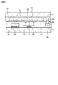
図3は、図2に示す表示装置を構成する発光素子10の一部分における模式的な一部断面図である。後で詳しく説明するが、発光素子10の駆動回路11を構成する各トランジスタ及び容量部C1は支持体20上に形成され、発光部ELPは、例えば、層間絶縁層40を介して、駆動回路11を構成する各トランジスタ及び容量部C1の上方に形成されている。発光部ELPは、例えば、アノード電極、正孔輸送層、発光層、電子輸送層、カソード電極等の周知の構成、構造を有する。尚、図3においては、駆動トランジスタTRDのみを図示する。他のトランジスタは隠れて見えない。また、駆動トランジスタTRDの他方のソース/ドレイン領域は、図示せぬ第4トランジスタTR4を介して発光部ELPに備えられたアノード電極に接続されているが、第4トランジスタTR4と発光部ELPのアノード電極との接続部も隠れて見えない。
FIG. 3 is a schematic partial cross-sectional view of a part of the light-emitting
駆動トランジスタTRDは、ゲート電極31、ゲート絶縁層32、半導体層33から構成されている。より具体的には、駆動トランジスタTRDは、半導体層33に設けられた一方のソース/ドレイン領域35及び他方のソース/ドレイン領域36、並びに、一方のソース/ドレイン領域35と他方のソース/ドレイン領域36の間の半導体層33の部分が該当するチャネル形成領域34を備えている。図示せぬ他のトランジスタも同様の構成である。
The drive transistor TR D includes a
容量部C1は、電極37、ゲート絶縁層32の延在部から構成された誘電体層、及び、電極38から成る。尚、電極37と駆動トランジスタTRDのゲート電極31との接続部、及び、電極38と給電線PS1との接続部は隠れて見えない。
The capacitive part C 1 includes an
ゲート電極31、ゲート絶縁層32の一部、及び、容量部C1を構成する電極37は、支持体20上に形成されている。駆動トランジスタTRD及び容量部C1等は、層間絶縁層40で覆われており、層間絶縁層40上に、アノード電極51、正孔輸送層、発光層、電子輸送層、及び、カソード電極53から成る発光部ELPが設けられている。尚、図3においては、正孔輸送層、発光層、及び、電子輸送層を1層52で表した。発光部ELPが設けられていない層間絶縁層40の部分の上には、第2層間絶縁層54が設けられ、第2層間絶縁層54及びカソード電極53上には透明な基板21が配置されており、発光層にて発光した光は、基板21を通過して、外部に出射される。カソード電極53と給電線PS2を構成する配線39とは、第2層間絶縁層54、層間絶縁層40に設けられたコンタクトホール56,55を介して接続されている。
The
図2に示す表示装置の製造方法を説明する。先ず、支持体20上に、走査線等の各種配線、容量部を構成する電極、半導体層から成るトランジスタ、層間絶縁層、コンタクトホール等を、周知の方法により適宜形成する。次いで、周知の方法により成膜及びパターニングを行い、マトリクス状に配列された発光部ELPを形成する。そして、上記工程を経た支持体20と基板21を対向させ周囲を封止し、表示装置を完成することができる。その後、必要に応じて外部の回路との結線を行えばよい。
A method for manufacturing the display device shown in FIG. 2 will be described. First, various wirings such as scanning lines, electrodes constituting a capacitor portion, transistors formed of a semiconductor layer, interlayer insulating layers, contact holes, and the like are appropriately formed on the
引き続き、図1及び図2を参照して、第m行、第n列目の発光素子10を構成する駆動回路11について説明する。書込みトランジスタTRWの他方のソース/ドレイン領域は、上述のとおり、駆動トランジスタTRDの一方のソース/ドレイン領域に接続されている。一方、書込みトランジスタTRWの一方のソース/ドレイン領域は、データ線DTLnに接続されている。書込みトランジスタTRWのオン/オフ動作は、書込みトランジスタTRWのゲート電極に接続された走査線SCLmからの信号によって制御される。
Next, with reference to FIG. 1 and FIG. 2, the drive circuit 11 constituting the
データ線DTLnには、信号出力回路102から、発光部ELPにおける輝度を制御するための映像信号(駆動信号、輝度信号)VSigが印加される。詳細については後述する。尚、データ線DTLを介して、VSig以外の種々の信号・電圧(プリチャージ駆動のための信号や各種の基準電圧等)が供給されてもよい。
A video signal (drive signal, luminance signal) V Sig for controlling the luminance in the light emitting unit ELP is applied from the
駆動トランジスタTRDは、発光素子10の発光状態においては、以下の式(1)に従ってドレイン電流Idsを流すように駆動される。発光素子10の発光状態においては、駆動トランジスタTRDの一方のソース/ドレイン領域はソース領域として働き、他方のソース/ドレイン領域はドレイン領域として働く。説明の便宜のため、以下の説明において、駆動トランジスタTRDの一方のソース/ドレイン領域を単にソース領域と呼び、他方のソース/ドレイン領域を単にドレイン領域と呼ぶ場合がある。尚、
μ :実効的な移動度
L :チャネル長
W :チャネル幅
Vgs:ゲート電極とソース領域との間の電位差
Vth:閾値電圧
Cox:(ゲート絶縁層の比誘電率)×(真空の誘電率)/(ゲート絶縁層の厚さ)
k≡(1/2)・(W/L)・Cox
とする。
The drive transistor TR D is driven so that the drain current I ds flows according to the following formula (1) when the
μ: Effective mobility L: Channel length W: Channel width V gs : Potential difference between gate electrode and source region V th : Threshold voltage C ox : (Relative permittivity of gate insulating layer) x (vacuum dielectric) Rate) / (gate insulating layer thickness)
k≡ (1/2) ・ (W / L) ・ C ox
And
Ids=k・μ・(Vgs−Vth)2 (1) I ds = k · μ · (V gs −V th ) 2 (1)
駆動回路11は、第2ノードND2と駆動トランジスタTRDの他方のソース/ドレイン領域との間に接続された第1スイッチ回路部SW1を備えている。第1スイッチ回路部SW1は第1トランジスタTR1から構成されている。第1トランジスタTR1にあっては、一方のソース/ドレイン領域は、第2ノードND2に接続されており、他方のソース/ドレイン領域は、駆動トランジスタTRDの他方のソース/ドレイン領域に接続されている。 The drive circuit 11 includes a first switch circuit unit SW 1 connected between the second node ND 2 and the other source / drain region of the drive transistor TR D. The first switch circuit unit SW 1 is composed of a first transistor TR 1 . In the first transistor TR 1 , one source / drain region is connected to the second node ND 2 , and the other source / drain region is connected to the other source / drain region of the driving transistor TR D. Has been.
背景技術において参照した図9に示す駆動回路では、第1スイッチ回路部SW1を構成する第1トランジスタTR1を走査線SCLmからの信号によって制御した。これに対し、実施例においては、第1トランジスタTR1のゲート電極は第1トランジスタ制御線CL1mに接続されている。第1トランジスタ制御線CL1mを介して、第1トランジスタ制御回路111から第1トランジスタTR1のゲート電極に信号を印加することにより、第1トランジスタTR1のオン状態/オフ状態を制御する。
In the drive circuit shown in FIG. 9 referred to in the background art, the first transistor TR 1 constituting the first switch circuit unit SW 1 is controlled by a signal from the scanning line SCL m . On the other hand, in the embodiment, the gate electrode of the first transistor TR 1 is connected to the first transistor control line CL1 m . By applying a signal from the first
駆動回路11は、更に、第2ノードND2と後述する所定の初期化電圧VIniが印加される給電線PS3との間に接続された第2スイッチ回路部SW2を備えている。第2スイッチ回路部SW2は第2トランジスタTR2から構成されている。第2トランジスタTR2にあっては、一方のソース/ドレイン領域は給電線PS3に接続されており、他方のソース/ドレイン領域は第2ノードND2に接続されている。 The drive circuit 11 further includes a second switch circuit unit SW 2 connected between the second node ND 2 and a feeder line PS 3 to which a predetermined initialization voltage V Ini described later is applied. The second switch circuit unit SW 2 is composed of a second transistor TR 2 . In the second transistor TR 2 , one source / drain region is connected to the feeder line PS 3 , and the other source / drain region is connected to the second node ND 2 .
第2トランジスタTR2の配線について更に説明する。第m番目の走査線SCLmよりも第P本分先行して走査される走査線をSCLm_pre_P(但し、Pは、1≦P<Mの関係を満たし、表示装置において所定の値)と表すとき、第m行目の発光素子10を構成する駆動回路11において、第2トランジスタTR2のゲート電極は走査線SCLm_pre_Pに接続されている。即ち、第2スイッチ回路部SW2を走査線SCLm_pre_Pからの走査信号により制御する。尚、実施例にあっては、P=1、即ち、直前に走査される走査線SCLm-1からの走査信号を第2トランジスタTR2のゲート電極に印加する。
The wiring of the second transistor TR 2 will be further described. A scanning line scanned P times ahead of the mth scanning line SCL m is represented as SCL m_pre_P (where P satisfies the
駆動回路11は、更に、第1ノードND1と後述する駆動電圧VCCが印加される給電線PS1との間に接続された第3スイッチ回路部SW3、及び、駆動トランジスタTRDの他方のソース/ドレイン領域と発光部ELPの一端との間に接続された第4スイッチ回路部SW4を備えている。第3スイッチ回路部SW3は第3トランジスタTR3から構成されている。第3トランジスタTR3にあっては、一方のソース/ドレイン領域は給電線PS1に接続されており、他方のソース/ドレイン領域は第1ノードND1に接続されている。第4スイッチ回路部SW4は第4トランジスタTR4から構成されている。第4トランジスタTR4にあっては、一方のソース/ドレイン領域は、駆動トランジスタTRDの他方のソース/ドレイン領域に接続されており、他方のソース/ドレイン領域は、発光部ELPの一端に接続されている。発光部ELPの他端(カソード電極)は、給電線PS2に接続されており、後述する電圧VCatが印加される。符号CELは発光部ELPの寄生容量を表す。 The drive circuit 11 further includes a third switch circuit unit SW 3 connected between the first node ND 1 and a feed line PS 1 to which a drive voltage V CC described later is applied, and the other of the drive transistor TR D. A fourth switch circuit unit SW 4 connected between the source / drain regions of the light emitting unit and one end of the light emitting unit ELP. The third switch circuit unit SW 3 is composed of a third transistor TR 3 . In the third transistor TR 3 , one source / drain region is connected to the feeder line PS 1 and the other source / drain region is connected to the first node ND 1 . The fourth switch circuit unit SW 4 is composed of a fourth transistor TR 4 . In the fourth transistor TR 4 , one source / drain region is connected to the other source / drain region of the driving transistor TR D , and the other source / drain region is connected to one end of the light emitting unit ELP. Has been. The other end of the light emitting portion ELP (cathode electrode) is connected to the feed line PS 2, voltage V Cat to be described later is applied. The symbol C EL represents the parasitic capacitance of the light emitting unit ELP.
背景技術において参照した図9に示す回路では、第3トランジスタTR3のゲート電極と第4トランジスタTR4のゲート電極とは同じ第3/第4トランジスタ制御線CLmに接続されていた。これに対し、実施例においては、第3トランジスタTR3のゲート電極は第3トランジスタ制御線CL3mに接続され、第4トランジスタTR4のゲート電極は第4トランジスタ制御線CL4mに接続されている。 In the circuit shown in FIG. 9 referred to in the background art, the gate electrode of the third transistor TR 3 and the gate electrode of the fourth transistor TR 4 are connected to the same third / fourth transistor control line CL m . On the other hand, in the embodiment, the gate electrode of the third transistor TR 3 is connected to the third transistor control line CL3 m, and the gate electrode of the fourth transistor TR 4 is connected to the fourth transistor control line CL4 m . .
実施例においては、第3トランジスタ制御線CL3mを介して、第3トランジスタ制御回路113から第3トランジスタTR3のゲート電極に信号を印加することにより、第3トランジスタTR3のオン状態/オフ状態を制御する。また、第4トランジスタ制御線CL4mを介して、第4トランジスタ制御回路114から第4トランジスタTR4のゲート電極に信号を印加することにより、第4トランジスタTR4のオン状態/オフ状態を制御する。
In the embodiment, the third transistor TR 3 is turned on / off by applying a signal from the third
第1トランジスタ制御回路111、第3トランジスタ制御回路113、及び、第4トランジスタ制御回路114の構成、構造は、周知の構成、構造とすることができる。
The configurations and structures of the first
実施例の説明において、電圧あるいは電位の値を以下のとおりとするが、これは、あくまでも説明のための値であり、これらの値に限定されるものではない。 In the description of the embodiments, the value of voltage or potential is as follows. However, this is just a value for explanation and is not limited to these values.
VSig :発光部ELPにおける輝度を制御するための映像信号
・・・0ボルト(最高輝度)〜8ボルト(最低輝度)
VCC :給電線PS1に印加される駆動電圧
・・・10ボルト
VIni :給電線PS3に印加される、第2ノードND2の電位を初期化するための初期化電圧
・・・−4ボルト
Vth :駆動トランジスタTRDの閾値電圧
・・・2ボルト
VCat :給電線PS2に印加される電圧
・・・−10ボルト
V Sig : Video signal for controlling the luminance in the light emitting part ELP... 0 volt (maximum luminance) to 8 volt (minimum luminance)
V CC : Drive voltage applied to the feeder line PS 1 ... 10 volts V Ini : Initialization voltage for initializing the potential of the second node ND 2 applied to the feeder line PS 3. 4 volts V th : threshold voltage of the drive transistor TR D ... 2 volts V Cat : voltage applied to the feed line PS 2 ... -10 volts
以下、第m行、第n列目に位置する発光素子10に関して、表示装置の動作を説明するが、係る発光素子10を、以下、第(n,m)番目の発光素子10あるいは第(n,m)番目の副画素と呼ぶ。また、第m行目に配列された各発光素子10の水平走査期間(より具体的には、現表示フレームにおける第m番目の水平走査期間)を、以下、単に、第m番目の水平走査期間と呼ぶ。
Hereinafter, the operation of the display device will be described with respect to the light-emitting
表示装置の駆動のタイミングチャートを模式的に図4に示し、駆動回路11を構成する各トランジスタのオン/オフ状態等を模式的に図5の(A)及び(B)、図6の(A)及び(B)、並びに、図7に示す。 A driving timing chart of the display device is schematically shown in FIG. 4, and the on / off states of the transistors constituting the driving circuit 11 are schematically shown in FIGS. 5A and 5B and FIG. ) And (B) and FIG.
実施例の表示装置の駆動方法は、オン状態とされた第1スイッチ回路部SW1により第2ノードND2と駆動トランジスタTRDの他方のソース/ドレイン領域とを電気的に接続した状態で、第1ノードND1に所定の値の電圧を所定の時間印加し、以て、第2ノードND2の電位を変化させる第2ノード電位補正工程を具備する。具体的には、図4に示す[期間−TP2]において第2ノード電位補正を行う。 The driving method of a display device of the embodiment, while electrically connecting the the first switch circuit SW 1 which is turned on the other of the source / drain regions of the second node ND 2 and the driving transistor TR D, A second node potential correction step of changing a potential of the second node ND 2 by applying a voltage of a predetermined value to the first node ND 1 for a predetermined time is provided. Specifically, the second node potential correction is performed in [period-TP 2 ] shown in FIG.
実施例の駆動方法は、オン状態とされた第1スイッチ回路部SW1により第2ノードND2と駆動トランジスタTRDの他方のソース/ドレイン領域とを電気的に接続した状態で、走査線SCLmからの信号によりオン状態とされた書込みトランジスタTRWを介して、データ線DTLnから第1ノードND1に映像信号VSigを印加し、以て、映像信号VSigから駆動トランジスタTRDの閾値電圧Vthを減じた電位に向かって第2ノードND2の電位を変化させる書込み工程を具備する。尚、第2ノードND2の電位を所定の基準電位に設定する初期化工程を行い、次いで、上述した書込み工程を行い、その後、上述した第2ノード電位補正工程を行う。具体的には、図4に示す[期間−TP0]において初期化工程を行い、[期間−TP1]において書込み工程を行う。 In the driving method of the embodiment, the scanning line SCL is in a state where the second node ND 2 and the other source / drain region of the driving transistor TR D are electrically connected by the first switch circuit unit SW 1 turned on. via the writing transistor TR W that is turned on by a signal from m, the video signal V Sig is applied from the data line DTL n to the first node ND 1, than Te, the driving transistor TR D from the video signal V Sig A writing step of changing the potential of the second node ND 2 toward the potential obtained by reducing the threshold voltage V th is provided. An initialization process for setting the potential of the second node ND 2 to a predetermined reference potential is performed, then the above-described writing process is performed, and then the above-described second node potential correction process is performed. Specifically, an initialization process is performed in [Period-TP 0 ] shown in FIG. 4, and a writing process is performed in [Period-TP 1 ].
実施例の駆動方法は、第1ノードND1に所定の駆動電圧VCCを印加し、以て、駆動トランジスタTRDを介して電流を発光部ELPに流すことにより発光部ELPを駆動する発光工程を具備する。尚、第2ノード電位補正工程において、第1ノードND1に所定の値の電圧として駆動電圧VCCを印加する。具体的には、図4に示す[期間−TP3]以降が発光工程に対応する。以下、図4に示す各期間の動作について、詳細に説明する。 In the driving method of the embodiment, a predetermined driving voltage V CC is applied to the first node ND 1 , and a current is caused to flow through the driving transistor TR D to drive the light emitting unit ELP. It comprises. In the second node potential correction step, the drive voltage V CC is applied to the first node ND 1 as a predetermined voltage. Specifically, the period after [period-TP 3 ] shown in FIG. 4 corresponds to the light emitting process. Hereinafter, the operation in each period shown in FIG. 4 will be described in detail.
[期間−TP-1](図4、図5の(A)参照)
この[期間−TP-1]は、従前に書き込まれた映像信号V’Sigに対応して、第(n,m)番目の発光素子10が発光状態にある期間である。第3トランジスタTR3と第4トランジスタTR4はオン状態である。書込みトランジスタTRW、第1トランジスタTR1、及び、第2トランジスタTR2はオフ状態である。第(n,m)番目の副画素を構成する発光素子10における発光部ELPには、後述する式(5)に基づくドレイン電流I’dsが流れており、第(n,m)番目の副画素を構成する発光素子10の輝度は、係るドレイン電流I’dsに対応した値である。
[Period-TP −1 ] (see FIGS. 4 and 5A)
This [period-TP −1 ] is a period in which the (n, m) th
[期間−TP0](図4、図5の(B)参照)
この[期間−TP0]は、現表示フレームにおける第(m−1)番目の水平走査期間である。この期間に、第1スイッチ回路部SW1、第3スイッチ回路部SW3、及び、第4スイッチ回路部SW4をオフ状態に維持し、オン状態とされた第2スイッチ回路部SW2を介して所定の初期化電圧VIniが印加される給電線PS2から第2ノードND2に所定の初期化電圧VIniを印加した後、第2スイッチ回路部SW2をオフ状態とし、以て、第2ノードND2の電位を所定の基準電位に設定する初期化工程を行う。
[Period -TP 0 ] (see FIGS. 4 and 5B)
This [period-TP 0 ] is the (m−1) th horizontal scanning period in the current display frame. During this period, the first switch circuit unit SW 1 , the third switch circuit unit SW 3 , and the fourth switch circuit unit SW 4 are maintained in the off state, and the second switch circuit unit SW 2 is turned on. after applying a predetermined initialization voltage V Ini from the feed line PS 2 to predetermined initialization voltage V Ini is applied to the second node ND 2 Te, the second switch circuit SW 2 is turned off, than Te, An initialization process for setting the potential of the second node ND 2 to a predetermined reference potential is performed.
具体的には、書込みトランジスタTRW及び第1トランジスタTR1のオフ状態を維持し、第3トランジスタTR3及び第4トランジスタTR4をオン状態からオフ状態とする。これにより、第1ノードND1には駆動電圧VCCが印加されず、更には、発光部ELPと駆動トランジスタTRDは切り離された状態となる。従って、発光部ELPに電流は流れず非発光状態となる。また、第2トランジスタTR2をオフ状態からオン状態とし、第2ノードND2にオン状態とされた第2トランジスタTR2を介して給電線PS2から所定の初期化電圧VIniを印加する。そして、例えばこの期間の終期に第2トランジスタTR2をオフ状態とする。容量部C1の一端には駆動電圧VCCが印加され、容量部C1の一端の電位は保たれた状態にあるので、第2ノードND2の電位は初期化電圧VIniにより所定の基準電位(−4ボルト)に設定される。 Specifically, the write transistor TR W and the first transistor TR 1 are kept off, and the third transistor TR 3 and the fourth transistor TR 4 are changed from the on state to the off state. As a result, the drive voltage V CC is not applied to the first node ND 1 , and the light emitting unit ELP and the drive transistor TR D are disconnected. Therefore, no current flows through the light emitting part ELP and the light emitting part ELP enters a non-light emitting state. Further, the second transistor TR 2 is changed from the OFF state to the ON state, and a predetermined initialization voltage V Ini is applied from the feeder line PS 2 to the second node ND 2 via the second transistor TR 2 that is turned ON. For example, the second transistor TR 2 is turned off at the end of this period. One end of the capacitor C 1 is applied drive voltage V CC is, since the potential of one end of the capacitor C 1 is in a state kept, a predetermined reference by the potential of the second node ND 2 initialization voltage V Ini Set to potential (-4 volts).
[期間−TP1](図4、図6の(A)参照)
この[期間−TP1]は、現表示フレームにおける第m番目の水平走査期間である。この期間に、第2スイッチ回路部SW2、第3スイッチ回路部SW3、及び、第4スイッチ回路部SW4のオフ状態を維持し、第1スイッチ回路部SW1をオン状態とし、オン状態とされた第1スイッチ回路部SW1により第2ノードND2と駆動トランジスタTRDの他方のソース/ドレイン領域とを電気的に接続した状態で、走査線SCLmからの信号によりオン状態とされた書込みトランジスタTRWを介して、データ線DTLnから第1ノードND1に映像信号VSigを印加し、以て、映像信号VSigから駆動トランジスタTRDの閾値電圧Vthを減じた電位に向かって第2ノードND2の電位を変化させる書込み工程を行う。
[Period-TP 1 ] (see FIGS. 4 and 6A)
This [period-TP 1 ] is the mth horizontal scanning period in the current display frame. During this period, the second switch circuit unit SW 2 , the third switch circuit unit SW 3 , and the fourth switch circuit unit SW 4 are maintained in the off state, the first switch circuit unit SW 1 is turned on, and the on state is established. In a state where the second node ND 2 and the other source / drain region of the driving transistor TR D are electrically connected by the first switch circuit unit SW 1 , the ON state is set by a signal from the scanning line SCL m. The video signal V Sig is applied from the data line DTL n to the first node ND 1 via the write transistor TR W, so that the potential obtained by subtracting the threshold voltage V th of the drive transistor TR D from the video signal V Sig is obtained. A writing process for changing the potential of the second node ND 2 is performed.
具体的には、第2トランジスタTR2、第3トランジスタTR3、及び、第4トランジスタTR4のオフ状態を維持し、走査線SCLmからの信号により書込みトランジスタTRWをオン状態とする。また、第1トランジスタ制御線CL1mからの信号により第1トランジスタTR1をオン状態とする。そして、オン状態とされた第1トランジスタTR1を介して第2ノードND2と駆動トランジスタTRDの他方のソース/ドレイン領域とを電気的に接続した状態とする。また、走査線SCLmからの信号によりオン状態とされた書込みトランジスタTRWを介して、データ線DTLnから第1ノードND1に映像信号VSigを印加する。これにより、映像信号VSigから駆動トランジスタTRDの閾値電圧Vthを減じた電位に向かって第2ノードND2の電位が変化する。 Specifically, the second transistor TR 2 , the third transistor TR 3 , and the fourth transistor TR 4 are kept off, and the write transistor TR W is turned on by a signal from the scanning line SCL m . Further, the first transistor TR 1 is turned on by a signal from the first transistor control line CL1 m . Then, the second node ND 2 and the other source / drain region of the driving transistor TR D are electrically connected via the first transistor TR 1 which is turned on. Further, the video signal V Sig is applied from the data line DTL n to the first node ND 1 via the write transistor TR W turned on by the signal from the scanning line SCL m . As a result, the potential of the second node ND 2 changes toward the potential obtained by subtracting the threshold voltage V th of the drive transistor TR D from the video signal V Sig .
即ち、上述した初期化により、[期間−TP1]の始期において駆動トランジスタTRDがオン状態となるように第2ノードND2の電位が初期化されているので、第2ノードND2の電位は、第1ノードND1に印加される映像信号VSigの電位に向かって変化する。しかしながら、駆動トランジスタTRDのゲート電極と一方のソース/ドレイン領域との間の電位差がVthに達すると、駆動トランジスタTRDはオフ状態となる。この状態にあっては、第2ノードND2の電位は、概ね(VSig−Vth)である。第2ノードND2の電位VND2は、以下の式(2)のように表される。尚、第(m+1)番目の水平走査期間が始まるより前に、走査線SCLmからの信号により書込みトランジスタTRWをオフ状態とする。 In other words, the initialization described above, since the second node potential of the ND 2 so that the driving transistor TR D is turned on at the beginning of [Period -TP 1] has been initialized, the second node ND 2 potential Changes toward the potential of the video signal V Sig applied to the first node ND 1 . However, when the potential difference between the gate electrode of the driving transistor TR D and one of the source / drain regions reaches V th , the driving transistor TR D is turned off. In this state, the potential of the second node ND 2 is approximately (V Sig −V th ). The potential V ND2 of the second node ND 2 is expressed as the following formula (2). Note that before the (m + 1) th horizontal scanning period starts, the write transistor TR W is turned off by a signal from the scanning line SCL m .
VND2≒(VSig−Vth) (2) V ND2 ≒ (V Sig -V th ) (2)
[期間−TP2](図4、図6の(B)参照)
この[期間−TP2]において、オン状態とされた第1スイッチ回路部SW1により第2ノードND2と駆動トランジスタTRDの他方のソース/ドレイン領域とを電気的に接続した状態で、第1ノードND1に所定の値の電圧を所定の時間印加し、以て、第2ノードND2の電位を変化させる第2ノード電位補正工程を行う。実施例では、第2ノード電位補正工程において、第1ノードND1に所定の値の電圧として駆動電圧VCCを印加する。
[Period -TP 2 ] (see FIGS. 4 and 6B)
In this [Period -TP 2 ], the second node ND 2 and the other source / drain region of the drive transistor TR D are electrically connected by the first switch circuit unit SW 1 turned on. A voltage having a predetermined value is applied to the first node ND 1 for a predetermined time, thereby performing a second node potential correction step of changing the potential of the second node ND 2 . In the embodiment, in the second node potential correction step, the driving voltage V CC is applied to the first node ND 1 as a voltage having a predetermined value.
具体的には、第1トランジスタTR1のオン状態を維持し、第3トランジスタTR3をオン状態とし、第1ノードND1に所定の値の電圧として駆動電圧VCCを[期間−TP2]の間印加する。尚、第2トランジスタTR2、及び、第4トランジスタTR4はオフ状態を維持する。以上の結果、駆動トランジスタTRDの移動度μの値が大きい場合、駆動トランジスタTRDのドレイン領域に接続された第2ノードND2の電位の上昇量ΔV(電位補正値)は大きくなり、駆動トランジスタTRDの移動度μの値が小さい場合、駆動トランジスタTRDのドレイン領域に接続された第2ノードND2の電位の上昇量ΔV(電位補正値)は小さくなる。ここで、第2ノードND2の電位VND2は、式(2)から以下の式(3)のように変形される。 Specifically, the ON state of the first transistor TR 1 is maintained, the third transistor TR 3 is turned ON, and the drive voltage V CC is applied to the first node ND 1 as a predetermined voltage [period-TP 2 ]. Apply during. Note that the second transistor TR 2 and the fourth transistor TR 4 are kept off. As a result, if the value of the mobility μ of the driving transistor TR D is large, the increase amount [Delta] V (potential correction value) of the second node ND 2 in the potential connected to the drain region of the drive transistor TR D becomes large, the driving When the value of the mobility μ of the transistor TR D is small, the amount of increase ΔV (potential correction value) of the potential of the second node ND 2 connected to the drain region of the driving transistor TR D is small. Here, the potential V ND2 of the second node ND 2 is transformed from the equation (2) into the following equation (3).
VND2≒(VSig−Vth)+ΔV (3) V ND2 ≈ (V Sig −V th ) + ΔV (3)
尚、第2ノード電位補正工程を実行するための所定の時間([期間−TP2]の全時間t0)は、表示装置の設計の際、設計値として予め決定しておけばよい。また、この第2ノード電位補正工程補正処理によって、係数k(≡(1/2)・(W/L)・Cox)のばらつきの補正も同時に行われる。 Note that a predetermined time for executing the second node potential correction step (total time t 0 of [period-TP 2 ]) may be determined in advance as a design value when designing the display device. In addition, the correction of the variation of the coefficient k (≡ (1/2) · (W / L) · C ox ) is simultaneously performed by the second node potential correction process correction process.
[期間−TP3](図4、図7参照)
この[期間−TP3]以降において、第1スイッチ回路部SW1をオフ状態とし、第2スイッチ回路部SW2のオフ状態を維持し、オン状態とされた第3スイッチ回路部SW3を介して第1ノードND1に所定の駆動電圧VCCを印加し、オン状態とされた第4スイッチ回路部SW4を介して駆動トランジスタTRDの他方のソース/ドレイン領域と発光部ELPの一端を電気的に接続し、以て、駆動トランジスタTRDを介して電流を発光部ELPに流すことにより発光部ELPを駆動する発光工程を行う。
[Period -TP 3 ] (See FIGS. 4 and 7)
After [Period -TP 3 ], the first switch circuit unit SW 1 is turned off, the second switch circuit unit SW 2 is kept off, and the third switch circuit unit SW 3 is turned on. Then, a predetermined drive voltage V CC is applied to the first node ND 1 , and the other source / drain region of the drive transistor TR D and one end of the light emitting unit ELP are connected via the fourth switch circuit unit SW 4 turned on. electrically connected, than Te, it emits light step of driving the light emitting section ELP by passing a current through the light emitting section ELP through the driving transistor TR D.
具体的には、[期間−TP3]の始期において第1トランジスタTR1をオフ状態とする。そして、第2トランジスタTR2のオフ状態を維持し、第3トランジスタTR3のオン状態を維持する。また、第4トランジスタ制御線CL4mからの信号により、第4トランジスタTR4をオフ状態からオン状態とする。オン状態とされた第3トランジスタTR3を介して第1ノードND1に所定の駆動電圧VCCを印加する。また、オン状態とされた第4トランジスタTR4を介して駆動トランジスタTRDの他方のソース/ドレイン領域と発光部ELPの一端を電気的に接続する。以て、駆動トランジスタTRDを介して電流を発光部ELPに流すことにより発光部ELPを駆動する。 Specifically, the first transistor TR 1 is turned off at the beginning of [Period -TP 3 ]. Then, the second transistor TR 2 is kept off and the third transistor TR 3 is kept on. Further, the fourth transistor TR 4 is changed from the off state to the on state by a signal from the fourth transistor control line CL 4 m . A predetermined drive voltage V CC is applied to the first node ND 1 through the third transistor TR 3 that is turned on. Moreover, to electrically connect the other of the source / drain regions of the driving transistor TR D through the fourth transistor TR 4 which is turned on and one end of the light emitting portion ELP. Accordingly, the light emitting unit ELP is driven by causing a current to flow through the light emitting unit ELP via the driving transistor TR D.
そして、式(3)より、
Vgs≒VCC−((VSig−Vth)+ΔV) (4)
であるから、上記式(1)は、
Ids=k・μ・(Vgs−Vth)2
=k・μ・((VCC−VSig)−ΔV)2 (5)
と表すことができる。
And from equation (3),
V gs ≈V CC − ((V Sig −V th ) + ΔV) (4)
Therefore, the above formula (1) is
I ds = k · μ · (V gs −V th ) 2
= K · μ · ((V CC −V Sig ) −ΔV) 2 (5)
It can be expressed as.
従って、発光部ELPを流れる電流Idsは、VCCとVSigとの電位差から、駆動トランジスタTRDの移動度μに起因した電位補正値ΔVの値を減じた値の2乗に比例する。云い換えれば、発光部ELPを流れる電流Idsは、駆動トランジスタTRDの閾値電圧Vthには依存しない。即ち、発光部ELPの発光量(輝度)は、駆動トランジスタTRDの閾値電圧Vthの影響を受けない。そして、第(n,m)番目の発光素子10の輝度は、係る電流Idsに対応した値である。
Therefore, the current I ds flowing through the light emitting unit ELP is proportional to the square of the value obtained by subtracting the value of the potential correction value ΔV caused by the mobility μ of the drive transistor TR D from the potential difference between V CC and V Sig . In other words, the current I ds flowing through the light emitting unit ELP does not depend on the threshold voltage V th of the drive transistor TR D. That is, the light emission amount (luminance) of the light emitting unit ELP is not affected by the threshold voltage V th of the drive transistor TR D. The luminance of the (n, m) th
しかも、移動度μの大きな駆動トランジスタTRDほど、電位補正値ΔVが大きくなる。従って、式(5)において、移動度μの値が大きくとも、((VCC−VSig)−ΔV)2の値が小さくなる結果、ドレイン電流Idsを補正することができる。即ち、移動度μの異なる駆動トランジスタTRDにおいても、映像信号VSigの値が同じであれば、ドレイン電流Idsが略同じとなる結果、発光部ELPを流れ、発光部ELPの輝度を制御する電流Idsが均一化される。これにより、移動度μのばらつき(更には、kのばらつき)に起因する発光部ELPの輝度のばらつきを補正することができる。 In addition, the potential correction value ΔV increases as the driving transistor TR D has a higher mobility μ. Therefore, in the equation (5), even if the value of the mobility μ is large, the value of ((V CC −V Sig ) −ΔV) 2 becomes small, so that the drain current I ds can be corrected. That is, even in the drive transistors TR D having different mobility μ, if the value of the video signal V Sig is the same, the drain current I ds is substantially the same, and as a result, the light flows through the light emitting unit ELP and controls the luminance of the light emitting unit ELP. The current I ds to be made uniform. As a result, it is possible to correct the luminance variation of the light emitting unit ELP caused by the variation in mobility μ (further, the variation in k).
発光部ELPの発光状態を次のフレームの第(m−2)番目の水平走査期間まで継続する。この時点は、[期間−TP-1]の終わりに相当する。 The light emission state of the light emitting unit ELP is continued until the (m-2) th horizontal scanning period of the next frame. This time point corresponds to the end of [period-TP −1 ].
以上によって、第(n,m)番目の副画素を構成する発光素子10の発光の動作が完了する。
Thus, the light emission operation of the
以上、本発明を好ましい実施例に基づき説明したが、本発明はこれらの実施例に限定されるものではない。実施例において説明した表示装置、発光素子、駆動回路を構成する各種の構成要素の構成、構造、発光部の駆動方法における工程は例示であり、適宜、変更することができる。 As mentioned above, although this invention was demonstrated based on the preferable Example, this invention is not limited to these Examples. The structure and structure of various components constituting the display device, the light emitting element, and the driving circuit described in the embodiments, and the steps in the method for driving the light emitting unit are examples, and can be changed as appropriate.
変形例として、図8に、第2スイッチ回路部を2本前に走査される走査線SCLm-2からの走査信号により制御する場合のタイミングチャートを示す。図8に示す[期間−TP’-1]〜[期間−TP’0]の動作は、初期化が第(m−2)番目の水平走査期間において行われる点が相違する他、図4を参照して説明した[期間−TP-1]〜[期間−TP0]の動作と同様である。 As a modification, FIG. 8 shows a timing chart in the case where the second switch circuit unit is controlled by the scanning signal from the scanning line SCL m-2 scanned two lines before. The operation of [Period-TP ′ −1 ] to [Period-TP ′ 0 ] shown in FIG. 8 is different in that initialization is performed in the (m−2) th horizontal scanning period, and FIG. The operation is the same as that in [period-TP −1 ] to [period-TP 0 ] described with reference to FIG.
図8に示す動作では、[期間−TP’1]において、全てのトランジスタのオフ状態を保ち、第1ノードND1が初期化された状態を保つ。そして、図8に示す[期間−TP’2]〜[期間−TP’4]において、図4を参照して説明した[期間−TP1]〜[期間−TP3]と同様の動作を行う。これにより、実施例において説明したと同様に、発光部ELPを駆動することができる。 In the operation illustrated in FIG. 8, in the [period-TP ′ 1 ], all the transistors are kept off and the first node ND 1 is initialized. Then, in [Period-TP ′ 2 ] to [Period-TP ′ 4 ] shown in FIG. 8, operations similar to [Period-TP 1 ] to [Period-TP 3 ] described with reference to FIG. 4 are performed. . Accordingly, the light emitting unit ELP can be driven as described in the embodiment.
SW1・・・第1スイッチ回路部、SW2・・・第2スイッチ回路部、SW3・・・第3スイッチ回路部、SW4・・・第4スイッチ回路部、TRW・・・書込みトランジスタ、TRD・・・駆動トランジスタ、TR1・・・第1トランジスタ、TR2・・・第2トランジスタ、TR3・・・第3トランジスタ、TR4・・・第4トランジスタ、C1・・・容量部、ELP・・・発光部、CEL・・・発光部ELPの容量、ND1・・・第1ノード、ND2・・・第2ノード、SCL・・・走査線、DTL・・・データ線、CL・・・第3/第4トランジスタ制御線、CL1・・・第1トランジスタ制御線、CL3・・・第3トランジスタ制御線、CL4・・・第4トランジスタ制御線、PS1・・・給電線、PS2・・・給電線、PS3・・・給電線、10・・・発光素子、11・・・駆動回路、20・・・支持体、21・・・基板、31・・・ゲート電極、32・・・ゲート絶縁層、33・・・半導体層、34・・・チャネル形成領域、35・・・一方のソース/ドレイン領域、36・・・他方のソース/ドレイン領域、37・・・一方の電極、38・・・他方の電極、39・・・配線、40・・・層間絶縁層、51・・・アノード電極、52・・・正孔輸送層、発光層及び電子輸送層、53・・・カソード電極、54・・・第2層間絶縁層、55,56・・・コンタクトホール、101・・・走査回路、102・・・信号出力回路、111・・・第1トランジスタ制御回路、113・・・第3トランジスタ制御回路、114・・・第4トランジスタ制御回路
SW 1 ... 1st switch circuit part, SW 2 ... 2nd switch circuit part, SW 3 ... 3rd switch circuit part, SW 4 ... 4th switch circuit part, TR W ... Write Transistor, TR D ... Driving transistor, TR 1 ... First transistor, TR 2 ... Second transistor, TR 3 ... Third transistor, TR 4 ... Fourth transistor, C 1.・ Capacitance part, ELP: Light emitting part, C EL : Capacity of light emitting part ELP, ND 1 ... First node, ND 2 ... Second node, SCL. Data line, CL ... third / fourth transistor control line, CL1 ... first transistor control line, CL3 ... third transistor control line, CL4 ... fourth transistor control line, PS 1 ... the power supply line, PS 2 ··· the power supply line, PS 3 ··· feed line, DESCRIPTION OF SYMBOLS 0 ... Light emitting element, 11 ... Drive circuit, 20 ... Support body, 21 ... Substrate, 31 ... Gate electrode, 32 ... Gate insulating layer, 33 ... Semiconductor layer, 34 ... Channel forming region, 35 ... One source / drain region, 36 ... Other source / drain region, 37 ... One electrode, 38 ... Other electrode, 39 ... Wiring , 40 ... interlayer insulating layer, 51 ... anode electrode, 52 ... hole transport layer, light emitting layer and electron transport layer, 53 ... cathode electrode, 54 ... second interlayer insulating layer, 55 56 ...
Claims (11)
(2)第1の方向に延びるM本の走査線、及び、
(3)第2の方向に延びるN本のデータ線、
を備えており、
各発光素子は、
(4)書込みトランジスタ、駆動トランジスタ、容量部、及び、第1スイッチ回路部を備えた駆動回路、並びに、
(5)駆動トランジスタを介して電流が流される発光部、
から構成されており、
書込みトランジスタにおいては、
(A−1)一方のソース/ドレイン領域は、データ線に接続されており、
(A−2)ゲート電極は、走査線に接続されており、
駆動トランジスタにおいては、
(B−1)一方のソース/ドレイン領域は、書込みトランジスタの他方のソース/ドレイン領域に接続されており、第1ノードを構成し、
容量部においては、
(C−1)一端には所定の基準電圧が印加され、
(C−2)他端と駆動トランジスタのゲート電極とは接続されており、第2ノードを構成し、
第1スイッチ回路部においては、
(D−1)一端は、第2ノードに接続されており、
(D−2)他端は、駆動トランジスタの他方のソース/ドレイン領域に接続されている、
表示装置の駆動方法であって、
オン状態とされた第1スイッチ回路部により第2ノードと駆動トランジスタの他方のソース/ドレイン領域とを電気的に接続した状態で、第1ノードに所定の値の電圧を所定の時間印加し、以て、第2ノードの電位を変化させる第2ノード電位補正工程、
を具備する表示装置の駆動方法。 (1) N elements in a first direction, M elements in a second direction different from the first direction, a total of N × M light emitting elements arranged in a two-dimensional matrix,
(2) M scanning lines extending in the first direction, and
(3) N data lines extending in the second direction;
With
Each light emitting element
(4) a drive circuit including a write transistor, a drive transistor, a capacitor, and a first switch circuit, and
(5) a light emitting section through which a current flows through the driving transistor;
Consists of
In the write transistor,
(A-1) One source / drain region is connected to the data line,
(A-2) The gate electrode is connected to the scanning line,
In the drive transistor,
(B-1) One source / drain region is connected to the other source / drain region of the write transistor and constitutes a first node;
In the capacity section,
(C-1) A predetermined reference voltage is applied to one end,
(C-2) The other end and the gate electrode of the driving transistor are connected to form a second node,
In the first switch circuit section,
(D-1) One end is connected to the second node,
(D-2) The other end is connected to the other source / drain region of the drive transistor.
A driving method of a display device,
A voltage of a predetermined value is applied to the first node for a predetermined time in a state where the second node and the other source / drain region of the driving transistor are electrically connected by the first switch circuit unit turned on. Thus, a second node potential correction step for changing the potential of the second node,
A driving method of a display device comprising:
を具備しており、
該書込み工程を行い、次いで、第2ノード電位補正工程を行う請求項1に記載の表示装置の駆動方法。 The second node and the other source / drain region of the driving transistor are electrically connected by the first switch circuit portion turned on via the write transistor turned on by the signal from the scanning line. A writing step of applying a video signal from the data line to the first node, thereby changing the potential of the second node toward the potential obtained by subtracting the threshold voltage of the driving transistor from the video signal;
It has
The display device driving method according to claim 1, wherein the writing step is performed, and then the second node potential correction step is performed.
を具備しており、
第2ノード電位補正工程を行い、次いで、該発光工程を行う請求項1に記載の表示装置の駆動方法。 A light emitting step of driving the light emitting unit by applying a predetermined driving voltage to the first node, and passing a current through the driving transistor to the light emitting unit;
It has
The method for driving a display device according to claim 1, wherein the second node potential correction step is performed, and then the light emission step is performed.
(E)第2ノードと所定の初期化電圧が印加される給電線との間に接続された第2スイッチ回路、
(F)第1ノードと駆動電圧が印加される給電線との間に接続された第3スイッチ回路部、及び、
(G)駆動トランジスタの他方のソース/ドレイン領域と発光部の一端との間に接続された第4スイッチ回路部、
を備えており、
(a)第1スイッチ回路部、第3スイッチ回路部、及び、第4スイッチ回路部をオフ状態に維持し、オン状態とされた第2スイッチ回路部を介して所定の初期化電圧が印加される給電線から第2ノードに所定の初期化電圧を印加した後、第2スイッチ回路部をオフ状態とし、以て、第2ノードの電位を所定の基準電位に設定する初期化工程を行い、
(b)次いで、第2スイッチ回路部、第3スイッチ回路部、及び、第4スイッチ回路部のオフ状態を維持し、第1スイッチ回路部をオン状態とし、オン状態とされた第1スイッチ回路部により第2ノードと駆動トランジスタの他方のソース/ドレイン領域とを電気的に接続した状態で、走査線からの信号によりオン状態とされた書込みトランジスタを介して、データ線から第1ノードに映像信号を印加し、以て、映像信号から駆動トランジスタの閾値電圧を減じた電位に向かって第2ノードの電位を変化させる書込み工程を行い、
(c)その後、走査線からの信号により書込みトランジスタをオフ状態とし、
(d)次いで、第1スイッチ回路部をオフ状態とし、第2スイッチ回路部のオフ状態を維持し、オン状態とされた第3スイッチ回路部を介して第1ノードに所定の駆動電圧を印加し、オン状態とされた第4スイッチ回路部を介して駆動トランジスタの他方のソース/ドレイン領域と発光部の一端を電気的に接続し、以て、駆動トランジスタを介して電流を発光部に流すことにより発光部を駆動する発光工程を行い、
更に、工程(c)と工程(d)との間に、第1スイッチ回路部のオン状態を維持し、第3スイッチ回路部をオン状態として、第1ノードに所定の値の電圧として駆動電圧を所定の時間印加し、以て、第2ノードの電位を変化させる第2ノード電位補正工程を行う請求項1に記載の表示装置の駆動方法。 The drive circuit is further
(E) a second switch circuit connected between the second node and a power supply line to which a predetermined initialization voltage is applied;
(F) a third switch circuit unit connected between the first node and the power supply line to which the drive voltage is applied, and
(G) a fourth switch circuit unit connected between the other source / drain region of the driving transistor and one end of the light emitting unit;
With
(A) The first switch circuit unit, the third switch circuit unit, and the fourth switch circuit unit are maintained in an off state, and a predetermined initialization voltage is applied through the second switch circuit unit in the on state. After applying a predetermined initialization voltage from the feeder line to the second node, the second switch circuit unit is turned off, thereby performing an initialization step of setting the potential of the second node to a predetermined reference potential,
(B) Next, the first switch circuit in which the second switch circuit unit, the third switch circuit unit, and the fourth switch circuit unit are maintained in the off state and the first switch circuit unit is in the on state. The video signal is transferred from the data line to the first node through the write transistor which is turned on by the signal from the scanning line in a state where the second node and the other source / drain region of the driving transistor are electrically connected by the unit. Applying a signal, and thus performing a writing step of changing the potential of the second node toward the potential obtained by subtracting the threshold voltage of the driving transistor from the video signal,
(C) Thereafter, the writing transistor is turned off by a signal from the scanning line,
(D) Next, the first switch circuit unit is turned off, the second switch circuit unit is kept off, and a predetermined drive voltage is applied to the first node via the third switch circuit unit turned on. Then, the other source / drain region of the drive transistor and one end of the light-emitting portion are electrically connected via the fourth switch circuit portion that is turned on, so that a current flows to the light-emitting portion via the drive transistor. To perform a light emitting process for driving the light emitting unit,
Further, between the step (c) and the step (d), the first switch circuit unit is kept on, the third switch circuit unit is turned on, and a driving voltage as a predetermined voltage is applied to the first node. 2. The display device driving method according to claim 1, wherein a second node potential correction step of changing the potential of the second node is performed by applying a predetermined time.
(2)第1の方向に延びるM本の走査線、及び、
(3)第2の方向に延びるN本のデータ線、
を備えており、
各発光素子は、
(4)書込みトランジスタ、駆動トランジスタ、容量部、及び、第1スイッチ回路部を備えた駆動回路、並びに、
(5)駆動トランジスタを介して電流が流される発光部。
から構成されており、
書込みトランジスタにおいては、
(A−1)一方のソース/ドレイン領域は、データ線に接続されており、
(A−2)ゲート電極は、走査線に接続されており、
駆動トランジスタにおいては、
(B−1)一方のソース/ドレイン領域は、書込みトランジスタの他方のソース/ドレイン領域に接続されており、第1ノードを構成し、
容量部においては、
(C−1)一端には所定の基準電圧が印加され、
(C−2)他端と駆動トランジスタのゲート電極とは接続されており、第2ノードを構成し、
第1スイッチ回路部においては、
(D−1)一端は、第2ノードに接続されており、
(D−2)他端は、駆動トランジスタの他方のソース/ドレイン領域に接続されている、
表示装置であって、
オン状態とされた第1スイッチ回路部により第2ノードと駆動トランジスタの他方のソース/ドレイン領域とを電気的に接続した状態で、第1ノードに所定の値の電圧を所定の時間印加し、以て、第2ノードの電位を変化させる表示装置。 (1) N elements in a first direction, M elements in a second direction different from the first direction, a total of N × M light emitting elements arranged in a two-dimensional matrix,
(2) M scanning lines extending in the first direction, and
(3) N data lines extending in the second direction;
With
Each light emitting element
(4) a drive circuit including a write transistor, a drive transistor, a capacitor, and a first switch circuit, and
(5) A light emitting unit through which a current flows through the driving transistor.
Consists of
In the write transistor,
(A-1) One source / drain region is connected to the data line,
(A-2) The gate electrode is connected to the scanning line,
In the drive transistor,
(B-1) One source / drain region is connected to the other source / drain region of the write transistor and constitutes a first node;
In the capacity section,
(C-1) A predetermined reference voltage is applied to one end,
(C-2) The other end and the gate electrode of the driving transistor are connected to form a second node,
In the first switch circuit section,
(D-1) One end is connected to the second node,
(D-2) The other end is connected to the other source / drain region of the drive transistor.
A display device,
A voltage of a predetermined value is applied to the first node for a predetermined time in a state where the second node and the other source / drain region of the driving transistor are electrically connected by the first switch circuit unit turned on. Thus, a display device that changes the potential of the second node.
Priority Applications (5)
| Application Number | Priority Date | Filing Date | Title |
|---|---|---|---|
| JP2008119838A JP2009271199A (en) | 2008-05-01 | 2008-05-01 | Display apparatus and driving method for display apparatus |
| TW098112199A TWI424409B (en) | 2008-05-01 | 2009-04-13 | Display apparatus and display-apparatus driving method |
| KR1020090033065A KR20090115661A (en) | 2008-05-01 | 2009-04-16 | Display apparatus and display-apparatus driving method |
| US12/385,689 US8294737B2 (en) | 2008-05-01 | 2009-04-16 | Display apparatus and display-apparatus driving method |
| CN200910138037XA CN101572055B (en) | 2008-05-01 | 2009-05-04 | Diaplay apparatus and display-apparatus driving method |
Applications Claiming Priority (1)
| Application Number | Priority Date | Filing Date | Title |
|---|---|---|---|
| JP2008119838A JP2009271199A (en) | 2008-05-01 | 2008-05-01 | Display apparatus and driving method for display apparatus |
Publications (2)
| Publication Number | Publication Date |
|---|---|
| JP2009271199A true JP2009271199A (en) | 2009-11-19 |
| JP2009271199A5 JP2009271199A5 (en) | 2011-05-06 |
Family
ID=41231396
Family Applications (1)
| Application Number | Title | Priority Date | Filing Date |
|---|---|---|---|
| JP2008119838A Pending JP2009271199A (en) | 2008-05-01 | 2008-05-01 | Display apparatus and driving method for display apparatus |
Country Status (5)
| Country | Link |
|---|---|
| US (1) | US8294737B2 (en) |
| JP (1) | JP2009271199A (en) |
| KR (1) | KR20090115661A (en) |
| CN (1) | CN101572055B (en) |
| TW (1) | TWI424409B (en) |
Families Citing this family (14)
| Publication number | Priority date | Publication date | Assignee | Title |
|---|---|---|---|---|
| JP2009288767A (en) * | 2008-05-01 | 2009-12-10 | Sony Corp | Display apparatus and driving method thereof |
| CN102693696B (en) * | 2011-04-08 | 2016-08-03 | 京东方科技集团股份有限公司 | Image element circuit structure and the method driving image element circuit structure |
| CN102915700B (en) * | 2011-08-04 | 2015-11-25 | 昆山维信诺显示技术有限公司 | Active oled lighting device |
| CN103975380B (en) * | 2011-12-09 | 2017-08-15 | 株式会社日本有机雷特显示器 | Display device, display panel and its driving method and electronic equipment |
| JP6282823B2 (en) * | 2013-09-02 | 2018-02-21 | 株式会社ジャパンディスプレイ | Driving circuit, display device, and driving method |
| CN103500556B (en) * | 2013-10-09 | 2015-12-02 | 京东方科技集团股份有限公司 | A kind of image element circuit and driving method, thin film transistor backplane |
| CN104751777B (en) | 2013-12-31 | 2017-10-17 | 昆山工研院新型平板显示技术中心有限公司 | Image element circuit, pixel and AMOLED display device and its driving method including the pixel |
| US10607542B2 (en) | 2013-12-31 | 2020-03-31 | Kunshan New Flat Panel Display Technology Center Co., Ltd. | Pixel circuit, pixel, and AMOLED display device comprising pixel and driving method thereof |
| JP6528267B2 (en) | 2014-06-27 | 2019-06-12 | Tianma Japan株式会社 | Pixel circuit and driving method thereof |
| KR20160011248A (en) * | 2014-07-21 | 2016-02-01 | 삼성디스플레이 주식회사 | Display panel and organic light emitting display device having the same |
| TWI638206B (en) * | 2015-09-01 | 2018-10-11 | 友達光電股份有限公司 | Active device array substrate |
| JP2017116576A (en) * | 2015-12-21 | 2017-06-29 | 株式会社ジャパンディスプレイ | Display device |
| US11532282B2 (en) | 2020-12-09 | 2022-12-20 | Apple Inc. | Displays with reduced temperature luminance sensitivity |
| WO2022125260A1 (en) * | 2020-12-09 | 2022-06-16 | Apple Inc. | Displays with reduced temperature luminance sensitivity |
Citations (2)
| Publication number | Priority date | Publication date | Assignee | Title |
|---|---|---|---|---|
| JP2005031630A (en) * | 2003-07-07 | 2005-02-03 | Samsung Sdi Co Ltd | Pixel circuit of organic electroluminescence display device, and its driving method |
| JP2009237558A (en) * | 2008-03-05 | 2009-10-15 | Semiconductor Energy Lab Co Ltd | Driving method for semiconductor device |
Family Cites Families (11)
| Publication number | Priority date | Publication date | Assignee | Title |
|---|---|---|---|---|
| KR100327374B1 (en) * | 2000-03-06 | 2002-03-06 | 구자홍 | an active driving circuit for a display panel |
| TWI252455B (en) * | 2004-01-29 | 2006-04-01 | Wintek Corp | Driving circuit for active matrix OLED |
| JP4103850B2 (en) * | 2004-06-02 | 2008-06-18 | ソニー株式会社 | Pixel circuit, active matrix device, and display device |
| JP2005352063A (en) * | 2004-06-09 | 2005-12-22 | Mitsubishi Electric Corp | Image display apparatus |
| JP2006106141A (en) * | 2004-09-30 | 2006-04-20 | Sanyo Electric Co Ltd | Organic el pixel circuit |
| KR100624137B1 (en) * | 2005-08-22 | 2006-09-13 | 삼성에스디아이 주식회사 | Pixel circuit of organic electroluminiscence display device and driving method the same |
| JP2008139520A (en) * | 2006-12-01 | 2008-06-19 | Sony Corp | Display device |
| JP2008164796A (en) * | 2006-12-27 | 2008-07-17 | Sony Corp | Pixel circuit and display device and driving method thereof |
| JP2009157019A (en) * | 2007-12-26 | 2009-07-16 | Sony Corp | Display device and electronic equipment |
| JP2009271200A (en) * | 2008-05-01 | 2009-11-19 | Sony Corp | Display apparatus and driving method for display apparatus |
| JP2009288767A (en) * | 2008-05-01 | 2009-12-10 | Sony Corp | Display apparatus and driving method thereof |
-
2008
- 2008-05-01 JP JP2008119838A patent/JP2009271199A/en active Pending
-
2009
- 2009-04-13 TW TW098112199A patent/TWI424409B/en not_active IP Right Cessation
- 2009-04-16 KR KR1020090033065A patent/KR20090115661A/en not_active Application Discontinuation
- 2009-04-16 US US12/385,689 patent/US8294737B2/en not_active Expired - Fee Related
- 2009-05-04 CN CN200910138037XA patent/CN101572055B/en not_active Expired - Fee Related
Patent Citations (2)
| Publication number | Priority date | Publication date | Assignee | Title |
|---|---|---|---|---|
| JP2005031630A (en) * | 2003-07-07 | 2005-02-03 | Samsung Sdi Co Ltd | Pixel circuit of organic electroluminescence display device, and its driving method |
| JP2009237558A (en) * | 2008-03-05 | 2009-10-15 | Semiconductor Energy Lab Co Ltd | Driving method for semiconductor device |
Also Published As
| Publication number | Publication date |
|---|---|
| CN101572055A (en) | 2009-11-04 |
| US20090273617A1 (en) | 2009-11-05 |
| CN101572055B (en) | 2012-02-08 |
| US8294737B2 (en) | 2012-10-23 |
| TW201001376A (en) | 2010-01-01 |
| TWI424409B (en) | 2014-01-21 |
| KR20090115661A (en) | 2009-11-05 |
Similar Documents
| Publication | Publication Date | Title |
|---|---|---|
| JP2009271200A (en) | Display apparatus and driving method for display apparatus | |
| JP2009271199A (en) | Display apparatus and driving method for display apparatus | |
| JP5870546B2 (en) | Display device and electronic device | |
| US8988325B2 (en) | Display device that switches light emission states multiple times during one field period | |
| JP2009288767A (en) | Display apparatus and driving method thereof | |
| JP5278119B2 (en) | Driving method of display device | |
| JP4844634B2 (en) | Driving method of organic electroluminescence light emitting unit | |
| JP5262930B2 (en) | Display element driving method and display device driving method | |
| JP4957713B2 (en) | Driving method of organic electroluminescence display device | |
| JP2009063719A (en) | Method of driving organic electroluminescence emission part | |
| JP2008226491A (en) | Organic electroluminescent display device | |
| JP5141192B2 (en) | Driving method of organic electroluminescence light emitting unit | |
| JP2008233502A (en) | Driving method of organic electroluminescence light emission part | |
| JP2008233501A (en) | Driving method of organic electroluminescence light emission part | |
| JP2010113188A (en) | Organic electroluminescence emitting unit driving method | |
| US8094252B2 (en) | Display apparatus and method for driving the same | |
| JP5293417B2 (en) | Driving method of display device | |
| JP4844641B2 (en) | Display device and driving method thereof | |
| JP2010181788A (en) | Display device and its driving method | |
| JP2009047718A (en) | Organic electroluminescence display device, drive circuit for driving organic electroluminescence light emitting part, and method for driving organic electroluminescence light emitting part | |
| JP2008281612A (en) | Driving circuit for driving organic electroluminescent light emitting unit, method for driving organic electroluminescent light emitting unit, and organic electroluminescent display device | |
| JP2011007842A (en) | Display device and method for driving the same | |
| JP2009098166A (en) | Method of driving organic electroluminescence emitting section | |
| JP2011007843A (en) | Display device and method for driving the same | |
| JP2008242369A (en) | Organic electroluminescence device and organic electroluminescence display device |
Legal Events
| Date | Code | Title | Description |
|---|---|---|---|
| RD02 | Notification of acceptance of power of attorney |
Free format text: JAPANESE INTERMEDIATE CODE: A7422 Effective date: 20100805 |
|
| A521 | Request for written amendment filed |
Free format text: JAPANESE INTERMEDIATE CODE: A523 Effective date: 20110317 |
|
| A621 | Written request for application examination |
Free format text: JAPANESE INTERMEDIATE CODE: A621 Effective date: 20110317 |
|
| A977 | Report on retrieval |
Free format text: JAPANESE INTERMEDIATE CODE: A971007 Effective date: 20120607 |
|
| A131 | Notification of reasons for refusal |
Free format text: JAPANESE INTERMEDIATE CODE: A131 Effective date: 20120626 |
|
| A02 | Decision of refusal |
Free format text: JAPANESE INTERMEDIATE CODE: A02 Effective date: 20121106 |