EP1496495B1 - Organic light emitting device pixel circuit with self-compensation of threshold voltage and driving method therefor - Google Patents
Organic light emitting device pixel circuit with self-compensation of threshold voltage and driving method therefor Download PDFInfo
- Publication number
- EP1496495B1 EP1496495B1 EP04090270.2A EP04090270A EP1496495B1 EP 1496495 B1 EP1496495 B1 EP 1496495B1 EP 04090270 A EP04090270 A EP 04090270A EP 1496495 B1 EP1496495 B1 EP 1496495B1
- Authority
- EP
- European Patent Office
- Prior art keywords
- transistor
- current
- gate
- signal
- light emitting
- Prior art date
- Legal status (The legal status is an assumption and is not a legal conclusion. Google has not performed a legal analysis and makes no representation as to the accuracy of the status listed.)
- Active
Links
- 238000000034 method Methods 0.000 title claims description 12
- 239000003990 capacitor Substances 0.000 claims description 27
- 239000010409 thin film Substances 0.000 description 10
- 229920001621 AMOLED Polymers 0.000 description 5
- 238000004519 manufacturing process Methods 0.000 description 5
- 238000010276 construction Methods 0.000 description 4
- 238000010586 diagram Methods 0.000 description 4
- 230000008901 benefit Effects 0.000 description 3
- 239000011159 matrix material Substances 0.000 description 2
- 230000015556 catabolic process Effects 0.000 description 1
- 238000006731 degradation reaction Methods 0.000 description 1
- 238000007599 discharging Methods 0.000 description 1
- 230000003071 parasitic effect Effects 0.000 description 1
- 239000000758 substrate Substances 0.000 description 1
Images


Classifications
-
- G—PHYSICS
- G09—EDUCATION; CRYPTOGRAPHY; DISPLAY; ADVERTISING; SEALS
- G09G—ARRANGEMENTS OR CIRCUITS FOR CONTROL OF INDICATING DEVICES USING STATIC MEANS TO PRESENT VARIABLE INFORMATION
- G09G3/00—Control arrangements or circuits, of interest only in connection with visual indicators other than cathode-ray tubes
- G09G3/20—Control arrangements or circuits, of interest only in connection with visual indicators other than cathode-ray tubes for presentation of an assembly of a number of characters, e.g. a page, by composing the assembly by combination of individual elements arranged in a matrix no fixed position being assigned to or needed to be assigned to the individual characters or partial characters
- G09G3/22—Control arrangements or circuits, of interest only in connection with visual indicators other than cathode-ray tubes for presentation of an assembly of a number of characters, e.g. a page, by composing the assembly by combination of individual elements arranged in a matrix no fixed position being assigned to or needed to be assigned to the individual characters or partial characters using controlled light sources
- G09G3/30—Control arrangements or circuits, of interest only in connection with visual indicators other than cathode-ray tubes for presentation of an assembly of a number of characters, e.g. a page, by composing the assembly by combination of individual elements arranged in a matrix no fixed position being assigned to or needed to be assigned to the individual characters or partial characters using controlled light sources using electroluminescent panels
- G09G3/32—Control arrangements or circuits, of interest only in connection with visual indicators other than cathode-ray tubes for presentation of an assembly of a number of characters, e.g. a page, by composing the assembly by combination of individual elements arranged in a matrix no fixed position being assigned to or needed to be assigned to the individual characters or partial characters using controlled light sources using electroluminescent panels semiconductive, e.g. using light-emitting diodes [LED]
- G09G3/3208—Control arrangements or circuits, of interest only in connection with visual indicators other than cathode-ray tubes for presentation of an assembly of a number of characters, e.g. a page, by composing the assembly by combination of individual elements arranged in a matrix no fixed position being assigned to or needed to be assigned to the individual characters or partial characters using controlled light sources using electroluminescent panels semiconductive, e.g. using light-emitting diodes [LED] organic, e.g. using organic light-emitting diodes [OLED]
- G09G3/3225—Control arrangements or circuits, of interest only in connection with visual indicators other than cathode-ray tubes for presentation of an assembly of a number of characters, e.g. a page, by composing the assembly by combination of individual elements arranged in a matrix no fixed position being assigned to or needed to be assigned to the individual characters or partial characters using controlled light sources using electroluminescent panels semiconductive, e.g. using light-emitting diodes [LED] organic, e.g. using organic light-emitting diodes [OLED] using an active matrix
- G09G3/3233—Control arrangements or circuits, of interest only in connection with visual indicators other than cathode-ray tubes for presentation of an assembly of a number of characters, e.g. a page, by composing the assembly by combination of individual elements arranged in a matrix no fixed position being assigned to or needed to be assigned to the individual characters or partial characters using controlled light sources using electroluminescent panels semiconductive, e.g. using light-emitting diodes [LED] organic, e.g. using organic light-emitting diodes [OLED] using an active matrix with pixel circuitry controlling the current through the light-emitting element
-
- G—PHYSICS
- G09—EDUCATION; CRYPTOGRAPHY; DISPLAY; ADVERTISING; SEALS
- G09G—ARRANGEMENTS OR CIRCUITS FOR CONTROL OF INDICATING DEVICES USING STATIC MEANS TO PRESENT VARIABLE INFORMATION
- G09G2300/00—Aspects of the constitution of display devices
- G09G2300/08—Active matrix structure, i.e. with use of active elements, inclusive of non-linear two terminal elements, in the pixels together with light emitting or modulating elements
- G09G2300/0809—Several active elements per pixel in active matrix panels
- G09G2300/0819—Several active elements per pixel in active matrix panels used for counteracting undesired variations, e.g. feedback or autozeroing
-
- G—PHYSICS
- G09—EDUCATION; CRYPTOGRAPHY; DISPLAY; ADVERTISING; SEALS
- G09G—ARRANGEMENTS OR CIRCUITS FOR CONTROL OF INDICATING DEVICES USING STATIC MEANS TO PRESENT VARIABLE INFORMATION
- G09G2300/00—Aspects of the constitution of display devices
- G09G2300/08—Active matrix structure, i.e. with use of active elements, inclusive of non-linear two terminal elements, in the pixels together with light emitting or modulating elements
- G09G2300/0809—Several active elements per pixel in active matrix panels
- G09G2300/0842—Several active elements per pixel in active matrix panels forming a memory circuit, e.g. a dynamic memory with one capacitor
- G09G2300/0861—Several active elements per pixel in active matrix panels forming a memory circuit, e.g. a dynamic memory with one capacitor with additional control of the display period without amending the charge stored in a pixel memory, e.g. by means of additional select electrodes
-
- G—PHYSICS
- G09—EDUCATION; CRYPTOGRAPHY; DISPLAY; ADVERTISING; SEALS
- G09G—ARRANGEMENTS OR CIRCUITS FOR CONTROL OF INDICATING DEVICES USING STATIC MEANS TO PRESENT VARIABLE INFORMATION
- G09G2310/00—Command of the display device
- G09G2310/02—Addressing, scanning or driving the display screen or processing steps related thereto
- G09G2310/0243—Details of the generation of driving signals
- G09G2310/0251—Precharge or discharge of pixel before applying new pixel voltage
-
- G—PHYSICS
- G09—EDUCATION; CRYPTOGRAPHY; DISPLAY; ADVERTISING; SEALS
- G09G—ARRANGEMENTS OR CIRCUITS FOR CONTROL OF INDICATING DEVICES USING STATIC MEANS TO PRESENT VARIABLE INFORMATION
- G09G2310/00—Command of the display device
- G09G2310/02—Addressing, scanning or driving the display screen or processing steps related thereto
- G09G2310/0262—The addressing of the pixel, in a display other than an active matrix LCD, involving the control of two or more scan electrodes or two or more data electrodes, e.g. pixel voltage dependent on signals of two data electrodes
-
- G—PHYSICS
- G09—EDUCATION; CRYPTOGRAPHY; DISPLAY; ADVERTISING; SEALS
- G09G—ARRANGEMENTS OR CIRCUITS FOR CONTROL OF INDICATING DEVICES USING STATIC MEANS TO PRESENT VARIABLE INFORMATION
- G09G2320/00—Control of display operating conditions
- G09G2320/04—Maintaining the quality of display appearance
- G09G2320/043—Preventing or counteracting the effects of ageing
- G09G2320/045—Compensation of drifts in the characteristics of light emitting or modulating elements
Definitions
- the present invention relates to a flat panel display and, more specifically, to a pixel circuit in an organic light emitting device capable of realizing high gradation by self-compensating a threshold voltage of a transistor that drives an electroluminescent (EL) element, and a method for driving the same.
- EL electroluminescent
- an organic light emitting device may be classified into a passive matrix organic light emitting diode (OLED) and an active matrix OLED (AMOLED), and can be classified into a current driving OLED and a voltage driving OLED depending on the manner in which the EL element is driven.
- OLED passive matrix organic light emitting diode
- AMOLED active matrix OLED
- a typical AMOLED is generally composed of a plurality of gate lines, a plurality of data lines, a plurality of power lines, and a plurality of pixels connected to the lines and arranged in a matrix form.
- Each pixel is normally composed of: an EL element; two transistors, in which one is a switching transistor for transferring a data signal while the other is a driving transistor for driving the EL element depending on the data signal; and one capacitor for maintaining the data voltage.
- this AMOLED has an advantage in that power consumption is low, current intensity flowing through the EL element changing over time, causing display nonuniformity, can be a problem. This results from a change in voltage between the gate and the source of the driving transistor for driving the EL element, namely, the threshold voltage of the driving transistor, which leads to a change in the current flowing through the EL element. Since the threshold voltage of a thin film transistor for the driving transistor changes depending on manufacturing process parameters, it becomes difficult to manufacture transistors in the AMOLED so that all of the transistors have the same threshold voltage. Thus, there are threshold voltage deviations between pixels.
- U.S. Patent No. 6,229,506 discloses an organic light emitting device for compensating the threshold voltage deviation.
- the '506 patent discloses a pixel structure in which a current source adjusts a voltage between the source and the gate of a driving transistor with respect to an overdrive voltage thereof and compensates the threshold voltage deviation of the driving transistor.
- the organic light emitting device in the '506 patent performs a two-step operation involving a data load (data write) step and a continuous light-emitting step, in which a current source adjusts a voltage between the source and the gate of the driving transistor with respect to the overdrive voltage and compensates the threshold voltage deviation of the driving transistor.
- the organic light emitting device as described above employs a current driving approach for driving the EL element which depends on a data signal current level applied from the current source and has difficulty in charging a data line. Because a parasitic capacitance of the data line is relatively large while the current level of the data signal provided from the current source is relatively small, the data becomes unstable as well as considerably long time x is required to charge the data line.
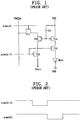
- Fig. 1 shows a pixel circuit of a voltage driving manner having a mirror type in a conventional voltage driving organic light emitting device.
- the pixel circuit comprises first P-type transistor T11 in which the gate of the first transistor is connected to current scan signal SCAN[n] applied to an associated scan line of a plurality of gate lines. Data signal VDATAm applied to an associated data line of a plurality of data lines is applied to its source. Second P-type transistor T12 in which a previous scan signal SCAN[n-1] is applied to a scan line just before the current scan line is applied to its gate. hitialization voltage Vinti is applied to its drain. Third and fourth P-type transistors T13 and T14 have a mirror type configuration. Fifth N-type transistor T15 in which previous scan signal SCAN[n-1] is applied to its gate has its drain coupled to the drain of fourth transistor T14. EL element EL11 is connected between fifth transistor T15 and ground voltage VSS. First capacitor C11 is connected between the gate and the source of fourth transistor T14.
- a scan line to be currently driven is the n-th scan line.
- a scan signal applied to the n-th scan line is SCAN[n].
- a scan line driven before the current scan line is the (n-1)th scan line.
- a scan signal applied to the (n-1)th scan line is SCAN[n-1].
- transistor T12 is turned on and transistors T11 and T15 are turned off, such that mirror-type transistors T13 and T14 are also turned off. Accordingly, the data stored in capacitor C11 is initialized through transistor T12 to initialization voltage Vinti.
- transistor T12 is turned off and transistor T11 is turned on, such that mirror-type transistors T13 and T14 are turned on.
- a data signal voltage level VDATAm applied to the data line is transferred through transistor T13 to the gate of driving transistor T14.
- transistor T15 is turned on by previous scan signal SCAN[n-1]
- a driving current corresponding to the data signal voltage VDATAm applied to the gate of driving transistor T14 flows into EL element EL 11 for its light-emitting.
- I EL 11 represents the current flowing through organic EL element EL 11
- V GS(T14) represents a voltage between the source and the gate of transistor T14
- V TH(13) represents a threshold voltage of transistor T13
- V DATA represents a data voltage
- ß represents a constant value, respectively.
- a compensating thin film transistor having a diode form is connected to a gate of the driving transistor in order to compensate the threshold voltage of the driving transistor.
- threshold voltages of the thin film transistor for compensation and the thin film transistor for driving EL element drive are different from each other, threshold voltage deviation of the driving transistor is not compensated, as well.
- the present invention therefore, addresses the aforementioned problem of the prior art, and provides a pixel circuit in an organic light emitting device capable of detecting and self-compensating threshold voltage deviations, and a method for driving the same, as recited in the appended claims.
- a pixel circuit in an organic light emitting device capable of compensating threshold voltage deviations regardless of manufacturing process parameters, and a method for driving the same.
- a pixel circuit in an organic light emitting device is provided which is capable of allowing a driving current flowing through an EL element to be uniform regardless of threshold voltage deviation between respective pixels, and a method for driving the same.
- a pixel circuit in an organic light emitting device capable of realizing high gradation representation regardless of threshold voltage deviation between respective pixels, and a method for driving the same.
- a pixel circuit in an organic light emitting device A first transistor delivers a data signal voltage in response to a current scan line signal. A second transistor generates a driving current depending an the data signal voltage delivered through the first transistor. A third transistor detects and self-compensates threshold voltage deviations in the second transistor. A capacitor for stores the data signal voltage delivered to the second transistor. An electroluminescent element emits light corresponding to the driving current generated through the 15 second transistor.
- a fourth transistor delivers a power supply voltage to the second transistor when the light is emitted.
- a fifth transistor delivers the driving current, provided from the second transistor, depending an the data signal voltage when the light is emitted.
- An electroluminescent element emits light corresponding to the driving current delivered through the fifth transistor.
- the third transistor connects the second transistor in the form of a diode in response to the current scan signal, so that the second transistor detects and compensates its threshold voltage deviation in itself.
- An initialization transistor composed of a PMOS transistor includes a gate to which a previous scan live signal is applied, a source coupled to a gate of the first transistor and one terminal of the capacitor and a a drain coupled to an initialization voltage supply for discharging the capacitor in response to the previous scan signal. It is the fourth transistor which characterizes the invention.
- the first transistor is composed of a PMOS transistor including a gate to which the current scan line signal is applied, a source to which the data signal voltage is applied, and a drain coupled to the second transistor.
- the second transistor is composed of a PMOS transistor including a gate coupled to one terminal of the capacitor, a source coupled to the first transistor, and a drain coupled to the electroluminescent element.
- the third transistor is composed of a PMOS transistor including a gate to which the current scan signal is applied, and a drain and a source which are coupled to the gate and the drain of the second transistor, respectively, so that the second transistor is connected in the form of a diode in response to the current scan signal to self-compensate a threshold voltage of the second transistor.
- the fourth transistor is composed of a PMOS transistor including a gate to which the current light-emitting signal is applied, a source to which a power supply voltage is applied, and a drain coupled to the second transistor.
- the fifth transistor is composed of a PMOS transistor including a gate to which the current light-emitting signal is applied, a source coupled to the second transistor, and a drain coupled to the electroluminescent element.
- An electroluminescent element emits light depending on an applied driving current.
- a first transistor delivers a data signal voltage in response to a current scan line signal.
- a second transistor for generates a driving current to drive the electroluminescent element in response to the data signal voltage.
- a third transistor connects the second transistor in the form of a diode in response to a current scan signal to self-compensate a threshold voltage of the second transistor.
- a capacitor stores the data signal voltage delivered to the second transistor.
- a fourth transistor delivers a power supply voltage to the second transistor in response to a current light-emitting signal.
- a fifth transistor provides the driving current, provided from the second transistor, for the electroluminescent element in response to the current light-emitting signal.
- a first transistor includes a gate to which a current scan signal is applied, and a source to which a data signal voltage is applied.
- a second transistor has its source coupled to a drain of the first transistor.
- a third transistor has its drain and source connected between a gate and a drain of the second transistor.
- a fourth transistor includes a gate to which a current light-emitting signal is applied, a source to which a power supply voltage is applied, and a drain coupled to the source of the second transistor.
- a fifth transistor includes a gate to which the current light-emitting signal is applied, a source coupled to the drain of the second transistor, and a drain coupled to one terminal of an electroluminescent element.
- the electroluminescent element has one terminal coupled to the drain of the fifth transistor and the other terminal grounded.
- a capacitor has one terminal coupled to the gate of the second transistor. A power supply voltage is applied to the other terminal of the capacitor.
- a pixel circuit in an organic light emitting device having a plurality of data lines, a plurality of scan lines, a plurality of power lines, and a plurality of pixels each connected to one associated data line, scan line and power line of the plurality of data lines, scan lines and power lines.
- Each pixel comprises: a first transistor including a gate to which a current scan signal to be applied to the associated scan line is applied, and a source to which a data signal voltage from the data line is applied; a second transistor whose source is coupled to a drain of the first transistor; a third transistor whose drain and source are connected between a gate and a drain of the second transistor, respectively; a fourth emitting transistor including a gate to which a current light-emitting signal is applied, a source to which a power supply voltage from the power line is applied, and a drain coupled to the source of the second transistor; a fifth transistor including a gate to which the current light-emitting signal is applied, and a source coupled to the drain of the second transistor; an electroluminescent element including one terminal coupled to the drain of the fifth transistor and the other terminal grounded; and a capacitor including one terminal coupled to the gate of the second transistor, and the other terminal to which the power supply voltage from the power line is applied.
- a method of driving a pixel in an organic light emitting device having a plurality of data lines, a plurality of scan lines, a plurality of power lines, and a plurality of pixels each connected to an associated one data line, scan line and power line of the plurality of data lines, scan lines and power lines.
- the method comprises: performing initialization in response to a scan signal applied to a scan line just before the associated scan line; compensating threshold voltage deviation in response to a scan signal applied to the associated scan line, and programming a data voltage applied from the associated data line, regardless of the threshold voltage deviation; and generating a driving current corresponding to the data voltage to emit an electroluminescent (EL) element in response to a current light-emitting signal.
- EL electroluminescent
- the organic light emitting device in accordance with the present invention includes a plurality of gate lines; a plurality of data lines; a plurality of power lines; and a plurality of pixels each arranged in an associated gate line, data line and power line of the plurality of gate lines, data lines and power lines.
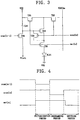
- Fig. 3 shows only one pixel arranged in an associated gate line (the n-th gate line), data line (the m-th data line) and power line (the m-th power line).
- each pixel in the organic light emitting device is composed of six transistors T31-T36, one capacitor C31 and electroluminescent (EL) element EL31. That is, each pixel includes organic electroluminescent device EL31 for emitting light corresponding to an applied driving current; first switching transistor T32 for switching data signal voltage VDATAm, applied to the associated data line, in response to current scan line signal SCAN[n] applied to the associated scan line; driving transistor T31 for supplying a driving current of the organic electroluminescent device corresponding to the data signal voltage inputted to its gate through first switching transistor T32; threshold voltage compensation transistor T33 for compensating the threshold voltage of driving transistor T31; and capacitor C31 for storing the data signal that is applied to the gate of driving transistor T31.
- first switching transistor T32 for switching data signal voltage VDATAm, applied to the associated data line, in response to current scan line signal SCAN[n] applied to the associated scan line
- driving transistor T31 for supplying a driving current of the organic electroluminescent device corresponding to the data signal voltage
- First switching transistor T32 is composed of a P-type thin film transistor in which current scan signal SCAN[n]. applied to the associated scan line, is applied to its gate, data signal voltage VDATAm. applied to the associated data line, is applied to its source, and its drain is connected to the source of driving transistor T31.
- Driving transistor T31 is composed of a P-type thin film transistor in which its gate is connected to one terminal of capacitor C31 and its drain is connected to one terminal of EL element EL31.
- Threshold voltage compensation transistor T33 is composed of a P-type thin film transistor in which its drain and source are connected to the gate and drain of driving transistor T31, respectively, and a current scan signal scan [n] is applied to the gate of transistor T33.
- Fbwer supply voltage VDD from the associated power line is provided for the other side of capacitor C31.
- each pixel comprises second switching transistor T35 for providing power supply voltage VDD for driving transistor T31 in response to current light-emitting signal EMI[n], and third switching transistor T36 for providing a driving current, generated through driving transistor T31, for EL element EL31 in response to current light-emitting signal EMI[n].
- Second switching transistor T35 is composed of a P-type thin film transistor in which current light-emitting signal EMI[n] is applied to its gate, the power supply voltage from the associated power supply voltage line is applied to its source, and its drain is connected to the source of driving transistor T31.
- Third switching transistor T36 is composed of a P-type thin film transistor in which current light-emitting signal EMI[n] is applied to its gate, its source is coupled to the drain of driving transistor T31, and the drain of transistor T36 is coupled to one terminal of EL element EL31. The other terminal of EL element EL31 is grounded.
- each pixel includes initialization transistor T34 for initializing the data signal stored in capacitor C31 in response to a previous scan signal SCAN[n-1] applied to a scan line just before the associated scan line.
- Transistor T34 is composed of a P-type thin film transistor in which previous scan signal SCAN[n-1] is applied to its gate, its source is coupled to the one terminal of capacitor C31, and initialization voltage Vinti is applied to its drain.
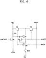
- switching transistor T32 is also turned on by current scan signal SCAN[n], and switching transistors T35 and T36 are turned off by current light-emitting signal EMI[n], such that a data program path (as indicated by a solid line shown in Fig. 6 ) is formed. Accordingly, data voltage VDATAm applied to the associated data line is provided for the gate of driving transistor T31 through threshold voltage compensation transistor T33.
- VDATAm-V TH(T31) is applied to the gate of transistor T31 and the gate voltage is stored in capacitor C31, such that the program operation is completed.
- I EL31 represents the current flowing into organic EL element EL31
- V GS represents a voltage between the source and the gate of transistor T31
- V TH(T31) represents a threshold voltage of transistor T31
- V DATA represents a data voltage
- ß represent a constant value, respectively.
- the driving current flows through EL element EL31, corresponding to the data signal voltage applied to the data line regardless of the threshold voltage of current driving transistor T31. That is, because the present invention detects and self-compensates the threshold voltage deviation in current driving transistor T31 throug h transistor T33, it is possible to finely control the current flowing into the organic EL element, thereby providing the high gradation of the organic EL element.
- the data signal can be no longer applied to the gate node of transistor T31 owing to the diode connection property of transistor T31, and thus switching transistor T34 is placed to initialize the gate node of transistor T31 into a predetermined level Vinti per frame.
- driving transistor T31 in the present invention can self-compensate the threshold voltage deviation by detecting its own threshold voltage.
- the embodiment of the present invention illustrates the pixel circuit composed of six transistors and one capacitor, the present invention is applicable to all constructions for detecting and self-compensating a threshold voltage.
- the pixel circuit can be configured of a NMOS transistor, a CMOS transistor or the like other than the PMOS transistor.
Landscapes
- Engineering & Computer Science (AREA)
- Physics & Mathematics (AREA)
- Computer Hardware Design (AREA)
- General Physics & Mathematics (AREA)
- Theoretical Computer Science (AREA)
- Control Of Indicators Other Than Cathode Ray Tubes (AREA)
- Control Of El Displays (AREA)
- Electroluminescent Light Sources (AREA)
Description
- This application claims the benefit of Korean Patent Application No.
2003-45610, filed Jul 7, 2003 - The present invention relates to a flat panel display and, more specifically, to a pixel circuit in an organic light emitting device capable of realizing high gradation by self-compensating a threshold voltage of a transistor that drives an electroluminescent (EL) element, and a method for driving the same.
- Normally, an organic light emitting device may be classified into a passive matrix organic light emitting diode (OLED) and an active matrix OLED (AMOLED), and can be classified into a current driving OLED and a voltage driving OLED depending on the manner in which the EL element is driven.
- A typical AMOLED is generally composed of a plurality of gate lines, a plurality of data lines, a plurality of power lines, and a plurality of pixels connected to the lines and arranged in a matrix form. Each pixel is normally composed of: an EL element; two transistors, in which one is a switching transistor for transferring a data signal while the other is a driving transistor for driving the EL element depending on the data signal; and one capacitor for maintaining the data voltage.
- Although this AMOLED has an advantage in that power consumption is low, current intensity flowing through the EL element changing over time, causing display nonuniformity, can be a problem. This results from a change in voltage between the gate and the source of the driving transistor for driving the EL element, namely, the threshold voltage of the driving transistor, which leads to a change in the current flowing through the EL element. Since the threshold voltage of a thin film transistor for the driving transistor changes depending on manufacturing process parameters, it becomes difficult to manufacture transistors in the AMOLED so that all of the transistors have the same threshold voltage. Thus, there are threshold voltage deviations between pixels.
- In order to solve this voltage deivation problem, a method has been developed for compensating the threshold voltage depending on manufacturing process parameters by adding a transistor for threshold voltage compensation.
U.S. Patent No. 6,229,506 ('506 patent) discloses an organic light emitting device for compensating the threshold voltage deviation. The '506 patent discloses a pixel structure in which a current source adjusts a voltage between the source and the gate of a driving transistor with respect to an overdrive voltage thereof and compensates the threshold voltage deviation of the driving transistor. The organic light emitting device in the '506 patent performs a two-step operation involving a data load (data write) step and a continuous light-emitting step, in which a current source adjusts a voltage between the source and the gate of the driving transistor with respect to the overdrive voltage and compensates the threshold voltage deviation of the driving transistor. - However, the organic light emitting device as described above employs a current driving approach for driving the EL element which depends on a data signal current level applied from the current source and has difficulty in charging a data line. Because a parasitic capacitance of the data line is relatively large while the current level of the data signal provided from the current source is relatively small, the data becomes unstable as well as considerably long time x is required to charge the data line.
- In order to solve the data line charging problem in the current driving approach, an organic light emitting device having a mirror type pixel structure has been proposed.
Fig. 1 shows a pixel circuit of a voltage driving manner having a mirror type in a conventional voltage driving organic light emitting device. - Referring to
Fig. 1 , the pixel circuit comprises first P-type transistor T11 in which the gate of the first transistor is connected to current scan signal SCAN[n] applied to an associated scan line of a plurality of gate lines. Data signal VDATAm applied to an associated data line of a plurality of data lines is applied to its source. Second P-type transistor T12 in which a previous scan signal SCAN[n-1] is applied to a scan line just before the current scan line is applied to its gate. hitialization voltage Vinti is applied to its drain. Third and fourth P-type transistors T13 and T14 have a mirror type configuration. Fifth N-type transistor T15 in which previous scan signal SCAN[n-1] is applied to its gate has its drain coupled to the drain of fourth transistor T14. EL element EL11 is connected between fifth transistor T15 and ground voltage VSS. First capacitor C11 is connected between the gate and the source of fourth transistor T14. - Operation of the pixel in the organic light emitting device having the above-described structure will be described with reference to an operation waveform diagram of
Fig. 2 . Here, it is assumed that a scan line to be currently driven is the n-th scan line. A scan signal applied to the n-th scan line is SCAN[n]. A scan line driven before the current scan line is the (n-1)th scan line. A scan signal applied to the (n-1)th scan line is SCAN[n-1]. - First of all, in initializing the operation, if predetermined levels of previous scan signal SCAN[n-1] and current scan signal SCAN[n] are applied thereto, that is, if a low level of previous scan signal SCAN[n-1] and a high level of current scan signal SCAN[n] are applied thereto, transistor T12 is turned on and transistors T11 and T15 are turned off, such that mirror-type transistors T13 and T14 are also turned off. Accordingly, the data stored in capacitor C11 is initialized through transistor T12 to initialization voltage Vinti.
- Meanwhile, in programming data, if predetermined levels of previous scan signal SCAN[n-1] and current scan signal are applied thereto, that is, if a high level of previous scan signal SCAN[n-1] and a low level of current scan signal SCAN[n] are applied thereto, transistor T12 is turned off and transistor T11 is turned on, such that mirror-type transistors T13 and T14 are turned on.
- Thus, a data signal voltage level VDATAm applied to the data line is transferred through transistor T13 to the gate of driving transistor T14. At this time, since transistor T15 is turned on by previous scan signal SCAN[n-1], a driving current corresponding to the data signal voltage VDATAm applied to the gate of driving transistor T14 flows into EL element EL 11 for its light-emitting.
- The voltage applied to the gate of transistor T14 becomes VDATA-VTH(T13), and the current flowing through EL element EL11 is represented by the following
Expression 1.
- Where, IEL 11 represents the current flowing through organic EL element EL 11, VGS(T14) represents a voltage between the source and the gate of transistor T14, VTH(13) represents a threshold voltage of transistor T13, VDATA represents a data voltage, and ß represents a constant value, respectively.
- At this time, if threshold voltages of transistors T13 and T14 for the current mirror are identical with each other, i.e., if VTH(T13)=VTH(T14), the threshold voltage of the transistor can be compensated, thereby maintaining the driving current of EL element EL 11 to be uniform.
- However, although transistors T13 and T14 configuring the current mirror are arranged adjacent to each other on a substrate in the voltage driving manner of the current mirror type as described above, it is very difficult to obtain the same threshold voltage due to the manufacturing process parameters of TFT. Therefore, there is a problem that it is difficult to obtain a uniform driving
current due to deviation of the threshold voltage of TFT, resulting in degraded Image quality.US publication 2003/0667424 describes an image Display including light emitting drive means driving light emitting means and a control switch for controlling light ON or light OFF. A technique for solving the Image quality degradation due to the threshold voltage deviation between TFTs for the current mirror in the voltage driving manner of the current mirror type as described above is disclosed inU.S. Patent No. 6,362,798 ('798 patent). In the '798 patent, a compensating thin film transistor having a diode form is connected to a gate of the driving transistor in order to compensate the threshold voltage of the driving transistor. However, there is a problem with the '798 patent that when threshold voltages of the thin film transistor for compensation and the thin film transistor for driving EL element drive are different from each other, threshold voltage deviation of the driving transistor is not compensated, as well. - The present invention, therefore, addresses the aforementioned problem of the prior art, and provides a pixel circuit in an organic light emitting device capable of detecting and self-compensating threshold voltage deviations, and a method for driving the same, as recited in the appended claims.
- Further in accordance with the present invention a pixel circuit in an organic light emitting device is provided capable of compensating threshold voltage deviations regardless of manufacturing process parameters, and a method for driving the same.
- Still further in accordance with the present invention a pixel circuit in an organic light emitting device is provided which is capable of allowing a driving current flowing through an EL element to be uniform regardless of threshold voltage deviation between respective pixels, and a method for driving the same.
- Yet still further in accordance with the present invention a pixel circuit in an organic light emitting device is provided capable of realizing high gradation representation regardless of threshold voltage deviation between respective pixels, and a method for driving the same.
- According to one aspect of the invention, there is provided a pixel circuit in an organic light emitting device. A first transistor delivers a data signal voltage in response to a current scan line signal. A second transistor generates a driving current depending an the data signal voltage delivered through the first transistor. A third transistor detects and self-compensates threshold voltage deviations in the second transistor. A capacitor for stores the data signal voltage delivered to the second transistor. An electroluminescent element emits light corresponding to the driving current generated through the 15 second transistor.
- A fourth transistor delivers a power supply voltage to the second transistor when the light is emitted. A fifth transistor delivers the driving
current, provided from the second transistor, depending an the data signal voltage when the light is emitted. An electroluminescent element emits light corresponding to the driving current delivered through the fifth transistor. The third transistor connects the second transistor in the form of a diode in response to the current scan signal, so that the second transistor detects and compensates its threshold voltage deviation in itself. An initialization transistor composed of a PMOS transistor includes a gate to which a previous scan live signal is applied, a source coupled to a gate of the first transistor and one terminal of the capacitor and a a drain coupled to an initialization voltage supply for discharging the capacitor in response to the previous scan signal. It is the fourth transistor which characterizes the invention. - In an embodiment the first transistor is composed of a PMOS transistor including a gate to which the current scan line signal is applied, a source to which the data signal voltage is applied, and a drain coupled to the second transistor. The second transistor is composed of a PMOS transistor including a gate coupled to one terminal of the capacitor, a source coupled to the first transistor, and a drain coupled to the electroluminescent element. The third transistor is composed of a PMOS transistor including a gate to which the current scan signal is applied, and a drain and a source which are coupled to the gate and the drain of the second transistor, respectively, so that the second transistor is connected in the form of a diode in response to the current scan signal to self-compensate a threshold voltage of the second transistor. The fourth transistor is composed of a PMOS transistor including a gate to which the current light-emitting signal is applied, a source to which a power supply voltage is applied, and a drain coupled to the second transistor. The fifth transistor is composed of a PMOS transistor including a gate to which the current light-emitting signal is applied, a source coupled to the second transistor, and a drain coupled to the electroluminescent element.
- According to yet another aspect of the invention, there is provided pixel circuit in an organic light emitting device. An electroluminescent element emits light depending on an applied driving current. A first transistor delivers a data signal voltage in response to a current scan line signal. A second transistor for generates a driving current to drive the electroluminescent element in response to the data signal voltage. A third transistor connects the second transistor in the form of a diode in response to a current scan signal to self-compensate a threshold voltage of the second transistor. A capacitor stores the data signal voltage delivered to the second transistor. A fourth transistor delivers a power supply voltage to the second transistor in response to a current light-emitting signal. A fifth transistor provides the driving current, provided from the second transistor, for the electroluminescent element in response to the current light-emitting signal.
- According to yet still another aspect of the invention, there is provided a pixel circuit in an organic light emitting device. A first transistor includes a gate to which a current scan signal is applied, and a source to which a data signal voltage is applied. A second transistor has its source coupled to a drain of the first transistor. A third transistor has its drain and source connected between a gate and a drain of the second transistor. A fourth transistor includes a gate to which a current light-emitting signal is applied, a source to which a power supply voltage is applied, and a drain coupled to the source of the second transistor. A fifth transistor includes a gate to which the current light-emitting signal is applied, a source coupled to the drain of the second transistor, and a drain coupled to one terminal of an electroluminescent element. The electroluminescent element has one terminal coupled to the drain of the fifth transistor and the other terminal grounded. A capacitor has one terminal coupled to the gate of the second transistor. A power supply voltage is applied to the other terminal of the capacitor.
- According to yet still another aspect of the invention, there is provided a pixel circuit in an organic light emitting device having a plurality of data lines, a plurality of scan lines, a plurality of power lines, and a plurality of pixels each connected to one associated data line, scan line and power line of the plurality of data lines, scan lines and power lines. Each pixel comprises: a first transistor including a gate to which a current scan signal to be applied to the associated scan line is applied, and a source to which a data signal voltage from the data line is applied; a second transistor whose source is coupled to a drain of the first transistor; a third transistor whose drain and source are connected between a gate and a drain of the second transistor, respectively; a fourth emitting transistor including a gate to which a current light-emitting signal is applied, a source to which a power supply voltage from the power line is applied, and a drain coupled to the source of the second transistor; a fifth transistor including a gate to which the current light-emitting signal is applied, and a source coupled to the drain of the second transistor; an electroluminescent element including one terminal coupled to the drain of the fifth transistor and the other terminal grounded; and a capacitor including one terminal coupled to the gate of the second transistor, and the other terminal to which the power supply voltage from the power line is applied.
- According to yet still another aspect of the invention, there is provided a method of driving a pixel in an organic light emitting device having a plurality of data lines, a plurality of scan lines, a plurality of power lines, and a plurality of pixels each connected to an associated one data line, scan line and power line of the plurality of data lines, scan lines and power lines. The method comprises: performing initialization in response to a scan signal applied to a scan line just before the associated scan line; compensating threshold voltage deviation in response to a scan signal applied to the associated scan line, and programming a data voltage applied from the associated data line, regardless of the threshold voltage deviation; and generating a driving current corresponding to the data voltage to emit an electroluminescent (EL) element in response to a current light-emitting signal.
-
-
Fig. 1 illustrates a circuit construction of a pixel in a conventional organic light emitting device. -
Fig. 2 is a waveform diagram for explaining operation of the pixel in the conventional organic light emitting device. -
Fig. 3 illustrates a circuit construction of a pixel in an organic light emitting device according to an embodiment of the present invention. -
Fig. 4 is a waveform diagram for explaining operation of the pixel in the organic light emitting device according to the embodiment of the present invention, as shown inFig. 3 . -
Figs. 5 to 7 are circuit construction diagrams for explaini ng initialization operation, program operation and light-emitting operation of a pixel in an organic light emitting device according to an embodiment of the present invention. - The organic light emitting device in accordance with the present invention includes a plurality of gate lines; a plurality of data lines; a plurality of power lines; and a plurality of pixels each arranged in an associated gate line, data line and power line of the plurality of gate lines, data lines and power lines.
Fig. 3 shows only one pixel arranged in an associated gate line (the n-th gate line), data line (the m-th data line) and power line (the m-th power line). - Referring to
Fig. 3 , each pixel in the organic light emitting device according to the present invention is composed of six transistors T31-T36, one capacitor C31 and electroluminescent (EL) element EL31. That is, each pixel includes organic electroluminescent device EL31 for emitting light corresponding to an applied driving current; first switching transistor T32 for switching data signal voltage VDATAm, applied to the associated data line, in response to current scan line signal SCAN[n] applied to the associated scan line; driving transistor T31 for supplying a driving current of the organic electroluminescent device corresponding to the data signal voltage inputted to its gate through first switching transistor T32; threshold voltage compensation transistor T33 for compensating the threshold voltage of driving transistor T31; and capacitor C31 for storing the data signal that is applied to the gate of driving transistor T31. - First switching transistor T32 is composed of a P-type thin film transistor in which current scan signal SCAN[n]. applied to the associated scan line, is applied to its gate, data signal voltage VDATAm. applied to the associated data line, is applied to its source, and its drain is connected to the source of driving transistor T31.
- Driving transistor T31 is composed of a P-type thin film transistor in which its gate is connected to one terminal of capacitor C31 and its drain is connected to one terminal of EL element EL31. Threshold voltage compensation transistor T33 is composed of a P-type thin film transistor in which its drain and source are connected to the gate and drain of driving transistor T31, respectively, and a current scan signal scan [n] is applied to the gate of transistor T33. Fbwer supply voltage VDD from the associated power line is provided for the other side of capacitor C31.
- Further, each pixel comprises second switching transistor T35 for providing power supply voltage VDD for driving transistor T31 in response to current light-emitting signal EMI[n], and third switching transistor T36 for providing a driving current, generated through driving transistor T31, for EL element EL31 in response to current light-emitting signal EMI[n].
- Second switching transistor T35 is composed of a P-type thin film transistor in which current light-emitting signal EMI[n] is applied to its gate, the power supply voltage from the associated power supply voltage line is applied to its source, and its drain is connected to the source of driving transistor T31. Third switching transistor T36 is composed of a P-type thin film transistor in which current light-emitting signal EMI[n] is applied to its gate, its source is coupled to the drain of driving transistor T31, and the drain of transistor T36 is coupled to one terminal of EL element EL31. The other terminal of EL element EL31 is grounded.
- Moreover, each pixel includes initialization transistor T34 for initializing the data signal stored in capacitor C31 in response to a previous scan signal SCAN[n-1] applied to a scan line just before the associated scan line. Transistor T34 is composed of a P-type thin film transistor in which previous scan signal SCAN[n-1] is applied to its gate, its source is coupled to the one terminal of capacitor C31, and initialization voltage Vinti is applied to its drain.
- Operation of the pixel having the above-described configuration according to the present invention will be described with reference to
Figs. 4 to 7 . - First, in an initialization operation, during an initialization period in which previous scan signal SCAN[n-1] is of a low level, and current scan signal SCAN[n] and light-emitting signal EMI[n] are of high level as shown in
Fig. 4 , since transistor T34 is turned on by the low level of previous scan signal SCAN[n-1], and transistors T31-T33 and T35-T36 are turned off by the high level of current scan signal SCAN[n] and current light-emitting signal EMI[n], an initialization path (as indicated by a solid line shown inFig. 5 ) is formed. Accordingly, the data signal that has been stored in capacitor C31, namely, a gate voltage of driving transistor T31, is initialized. - Next, in a data program operation, during a programming period in which previous scan signal scan [n-1] is at a high level, current scan signal SCAN[n] is at a low level and current light-emitting signal EMI[n] is at a high level as shown in
Fig. 4 , transistor T34 is turned off, and transistor T33 is turned on by the low level of current scan signal SCAN[n], such that driving transistor T31 is connected in the form of a diode. - Since switching transistor T32 is also turned on by current scan signal SCAN[n], and switching transistors T35 and T36 are turned off by current light-emitting signal EMI[n], such that a data program path (as indicated by a solid line shown in
Fig. 6 ) is formed. Accordingly, data voltage VDATAm applied to the associated data line is provided for the gate of driving transistor T31 through threshold voltage compensation transistor T33. - Since driving transistor T31 is in the diode connection, VDATAm-VTH(T31) is applied to the gate of transistor T31 and the gate voltage is stored in capacitor C31, such that the program operation is completed.
- Finally, in a light-emitting operation, during an light-emitting period in which previous scan signal SCAN[n-1] is of high level, current scan signal SCAN[n] becomes a high level, and then current light-emitting signal EMI[n] becomes a low level as shown in
Fig. 4 , an light-emitting path (as indicated by the solid line as shown inFig. 7 ) is formed. That is, switching transistors T35 and T36 are turned on by the low level of current light-emitting signal EMI[n], initialization transistor T34 is turned off by the high level of previous scan signal SCAN[n-1], and threshold voltage compensation transistor T33 and switching transistor T32 are turned off by the high level of current scan signal SCAN[n]. Accordingly, a driving current generated in response to the data signal voltage applied to the gate of driving transistor T31 is provided through transistor T31 for organic EL element EL31, such that the light-emitting of organic EL element EL31 occurs. - At this time, the current into organic EL element EL31 is represented by the following Expression 2.

- Where, IEL31 represents the current flowing into organic EL element EL31, VGS represents a voltage between the source and the gate of transistor T31, VTH(T31) represents a threshold voltage of transistor T31, VDATA represents a data voltage, and ß represent a constant value, respectively.
- As can be seen from the Expression 2, the driving current flows through EL element EL31, corresponding to the data signal voltage applied to the data line regardless of the threshold voltage of current driving transistor T31. That is, because the present invention detects and self-compensates the threshold voltage deviation in current driving transistor T31 throug h transistor T33, it is possible to finely control the current flowing into the organic EL element, thereby providing the high gradation of the organic EL element.
- Further, if the data for a previous frame time has a high level of voltage and the data for a next frame time has a low level of voltage, the data signal can be no longer applied to the gate node of transistor T31 owing to the diode connection property of transistor T31, and thus switching transistor T34 is placed to initialize the gate node of transistor T31 into a predetermined level Vinti per frame.
- As described above, driving transistor T31 in the present invention can self-compensate the threshold voltage deviation by detecting its own threshold voltage.
- Although the embodiment of the present invention illustrates the pixel circuit composed of six transistors and one capacitor, the present invention is applicable to all constructions for detecting and self-compensating a threshold voltage. Moreover, the pixel circuit can be configured of a NMOS transistor, a CMOS transistor or the like other than the PMOS transistor.
- According to the embodiment of the present invention as described above, there are advantages that it is possible to realize high gradation by detecting and self-compensating the threshold voltage deviation in the driving transistor as well as to solve a charging problem in the data line by driving the driving transistor in the voltage driving manner.
- Although the present invention has been described with reference to the exemplary embodiments thereof, it will be appreciated by those skilled in the art that it is possible to modify and change the present invention variously without departing from the scope of the present invention as set forth in the following claims.
Claims (10)
- A pixel circuit for an organic light emitting device, comprising:a first transistor (T 32) for delivering a voltage level of a data signal applied to its source in response to a current scan signal applied to its gate ;a second transistor (T 31) for generating a driving current depending on the voltage level of data signal delivered to its source through the first transistor;a third transistor (T 33) for connecting the second transistor in the form of a diode in response to the current scan signal applied to the gate of the third transistor (T 33);an electroluminescent element (EL 31) for emitting light corresponding to the driving current generated through the second transistor (T 31);a driving current providing transistor ( T 36) for providing the driving current for the electroluminescent element (EL 31) from the drain of the second transistor (T 31) in response to a current light-emitting signal applied to the gate of the driving current providing transistor ( T 36); and a capacitor (C 31) for storing the voltage level of the data signal delivered to the source of the second transistor (T 31), andan initialization transistor ( T 34) for initializing the voltage level stored in the capacitor (C 31) in response to a previous scan signal,wherein the initialization transistor (T 34) is a PMOS transistor,wherein the initialization transistor (T 34) includes a gate to which the previous scan line signal is applied, a source coupled to a gate of the second transistor (T 31) and a first terminal of the capacitor (C 31), and a drain coupled to an initialization voltage supply, characterized in that the pixel circuit further comprises a transistor (T 35) providing a power supply voltage to the second transistor (T 31) in response to a current light emitting signal of the power supply providing transistor (T35) and in that the drain of the first transistor (T32) is connected to the source of the second transistor (T31).
- The pixel circuit in the organic light emitting device of claim 1, wherein the first, second, and third transistors, the power supply providing transistor and the driving current providing transistor (T31, T 32, T 33, T 34, T35, T 36) are PMOS transistors.
- The pixel circuit in the organic light emitting device of claim 2, wherein the second transistor includes a gate coupled to the first terminal of the capacitor, a source coupled to the drain of the first transistor, and a drain coupled to the electroluminescent element.
- The pixel circuit in the organic light emitting device of claim 2, wherein the third transistor includes a gate to which the current scan signal is applied, and a drain and a source which are coupled to the gate and the drain of the second transistor, respectively.
- The pixel circuit in the organic light emitting device of claim 2, wherein the power supply providing transistor includes a gate to which the current light-emitting signal is applied, a source to which a power supply voltage is applied and coupled to the second terminal of the capacitor, and a drain coupled to the source of the second transistor and the drain of the first transistor.
- The pixel circuit in the organic light emitting device of claim 2, wherein the driving current providing transistor includes a gate to which the current light-emitting signal is applied, a source coupled to the drain of the second transistor, and a drain coupled to the electroluminescent element.
- The pixel circuit in the organic light emitting device of claim 1, further comprising:a voltage source for providing the voltage level of data signal through the first transistor for the second transistor.
- An organic light emitting display device comprising:a plurality of data lines extending in a first direction;a plurality of scan lines extending in a second direction crossing the first direction;a plurality of emission control lines; anda plurality of pixels each pixel comprising a pixel circuit according to one of the previous claims, each of the pixels being connected to a corresponding one of the plurality of data lines, a corresponding current scan line of the plurality of scan lines, a corresponding previous scan line of the plurality of scan lines and a corresponding one of the plurality of emission control lines.
- The organic light emitting display device of claim 8, further comprising a controller adapted to provide a first scan signal to the previous scan line during an initialization period, to provide a second scan signal to the current scan line during a programming period following the initialization period, and to provide an emission control signal to the corresponding one of the plurality of emission control lines during an emitting period following the programming period.
- A method of driving a pixel circuit according to one of claims 1-7, the pixel circuit being comprised in an organic light emitting device, the method comprising the steps of:connecting a driving transistor in the form of a diode to provide a data voltage to the gate of the driving transistor, and storing the data voltage in the capacitor in response to current scan signal; andgenerating a driving current corresponding to the data voltage to emit an electroluminescent element in response to a current light-emitting signal,further comprising the step of initializing a capacitor in response to a previous scan signal.
Applications Claiming Priority (2)
| Application Number | Priority Date | Filing Date | Title |
|---|---|---|---|
| KR2003045610 | 2003-07-07 | ||
| KR1020030045610A KR100560780B1 (en) | 2003-07-07 | 2003-07-07 | Pixel circuit in OLED and Method for fabricating the same |
Publications (4)
| Publication Number | Publication Date |
|---|---|
| EP1496495A2 EP1496495A2 (en) | 2005-01-12 |
| EP1496495A8 EP1496495A8 (en) | 2005-03-16 |
| EP1496495A3 EP1496495A3 (en) | 2007-05-23 |
| EP1496495B1 true EP1496495B1 (en) | 2017-01-04 |
Family
ID=33448349
Family Applications (1)
| Application Number | Title | Priority Date | Filing Date |
|---|---|---|---|
| EP04090270.2A Active EP1496495B1 (en) | 2003-07-07 | 2004-07-05 | Organic light emitting device pixel circuit with self-compensation of threshold voltage and driving method therefor |
Country Status (5)
| Country | Link |
|---|---|
| US (1) | US7414599B2 (en) |
| EP (1) | EP1496495B1 (en) |
| JP (1) | JP4391857B2 (en) |
| KR (1) | KR100560780B1 (en) |
| CN (1) | CN100386794C (en) |
Families Citing this family (303)
| Publication number | Priority date | Publication date | Assignee | Title |
|---|---|---|---|---|
| KR100637433B1 (en) | 2004-05-24 | 2006-10-20 | 삼성에스디아이 주식회사 | Light emitting display |
| JP2000031880A (en) * | 1998-07-16 | 2000-01-28 | Kokusai Electric Co Ltd | Radio repeater |
| CA2555286A1 (en) * | 2004-02-09 | 2005-08-25 | Bunn-O-Matic Corporation | Apparatus, system and method for infusing a pre-packaged pod |
| GB2411758A (en) * | 2004-03-04 | 2005-09-07 | Seiko Epson Corp | Pixel circuit |
| KR100560446B1 (en) | 2004-03-15 | 2006-03-13 | 삼성에스디아이 주식회사 | Light emitting display and driving method thereof |
| KR100560445B1 (en) * | 2004-03-15 | 2006-03-13 | 삼성에스디아이 주식회사 | Light emitting display and driving method thereof |
| KR101142994B1 (en) * | 2004-05-20 | 2012-05-08 | 삼성전자주식회사 | Display device and driving method thereof |
| KR100658616B1 (en) | 2004-05-31 | 2006-12-15 | 삼성에스디아이 주식회사 | Light emitting display device and display panel and driving method thereof |
| TW200620207A (en) * | 2004-07-05 | 2006-06-16 | Sony Corp | Pixel circuit, display device, driving method of pixel circuit, and driving method of display device |
| KR100592641B1 (en) * | 2004-07-28 | 2006-06-26 | 삼성에스디아이 주식회사 | Pixel circuit and organic light emitting display using the same |
| KR100673759B1 (en) * | 2004-08-30 | 2007-01-24 | 삼성에스디아이 주식회사 | Light emitting display |
| JP4160032B2 (en) | 2004-09-01 | 2008-10-01 | シャープ株式会社 | Display device and driving method thereof |
| KR100612392B1 (en) | 2004-10-13 | 2006-08-16 | 삼성에스디아이 주식회사 | Light emitting display and light emitting display panel |
| KR100606416B1 (en) * | 2004-11-17 | 2006-07-31 | 엘지.필립스 엘시디 주식회사 | Driving Apparatus And Method For Organic Light-Emitting Diode |
| KR100739318B1 (en) * | 2004-11-22 | 2007-07-12 | 삼성에스디아이 주식회사 | Pixel circuit and light emitting display |
| KR100688802B1 (en) * | 2004-11-22 | 2007-03-02 | 삼성에스디아이 주식회사 | Pixel and light emitting display |
| JP4364849B2 (en) * | 2004-11-22 | 2009-11-18 | 三星モバイルディスプレイ株式會社 | Luminescent display device |
| KR100688801B1 (en) | 2004-11-22 | 2007-03-02 | 삼성에스디아이 주식회사 | Delta pixel circuit and light emitting display |
| KR100604061B1 (en) * | 2004-12-09 | 2006-07-24 | 삼성에스디아이 주식회사 | Pixel circuit and light emitting display |
| KR100602363B1 (en) * | 2005-01-10 | 2006-07-18 | 삼성에스디아이 주식회사 | Emission driver and light emitting display for using the same |
| CN1822385B (en) | 2005-01-31 | 2013-02-06 | 株式会社半导体能源研究所 | Display device and electronic device comprising same |
| KR100642264B1 (en) * | 2005-02-04 | 2006-11-06 | 재단법인서울대학교산학협력재단 | Picture element structure of organic light emitting diode |
| KR101152120B1 (en) * | 2005-03-16 | 2012-06-15 | 삼성전자주식회사 | Display device and driving method thereof |
| KR100653846B1 (en) * | 2005-04-11 | 2006-12-05 | 실리콘 디스플레이 (주) | circuit and method for driving 0rganic Light-Emitting Diode |
| JP5392963B2 (en) * | 2005-04-19 | 2014-01-22 | インテレクチュアル キーストーン テクノロジー エルエルシー | Electro-optical device and electronic apparatus |
| KR100840116B1 (en) * | 2005-04-28 | 2008-06-20 | 삼성에스디아이 주식회사 | Light Emitting Diode Display |
| KR100731743B1 (en) * | 2005-04-29 | 2007-06-22 | 삼성에스디아이 주식회사 | Pixel Circuit of Organic Electoluminescent Display Device |
| US7872620B2 (en) * | 2005-04-29 | 2011-01-18 | Seoul National University Industry Foundation | Pixel structure using voltage programming-type for active matrix organic light emitting device |
| KR100719924B1 (en) * | 2005-04-29 | 2007-05-18 | 비오이 하이디스 테크놀로지 주식회사 | Organic electroluminescence display device |
| KR100782455B1 (en) * | 2005-04-29 | 2007-12-05 | 삼성에스디아이 주식회사 | Emission Control Driver and Organic Electro Luminescence Display Device of having the same |
| KR100683772B1 (en) * | 2005-05-13 | 2007-02-15 | 삼성에스디아이 주식회사 | Organic light emitting display device |
| KR100624314B1 (en) | 2005-06-22 | 2006-09-19 | 삼성에스디아이 주식회사 | Light emission display device and thin film transistor |
| TW200707385A (en) * | 2005-07-15 | 2007-02-16 | Seiko Epson Corp | Electronic device, method of driving the same, electro-optical device, and electronic apparatus |
| KR100547515B1 (en) * | 2005-07-27 | 2006-01-31 | 실리콘 디스플레이 (주) | Organic light emitting diode display and method for driving oled |
| KR100635509B1 (en) * | 2005-08-16 | 2006-10-17 | 삼성에스디아이 주식회사 | Organic electroluminescent display device |
| KR100636502B1 (en) * | 2005-08-31 | 2006-10-18 | 삼성에스디아이 주식회사 | Organic electro luminescence display for performing sheet unit test and testing method using the same |
| KR100666640B1 (en) * | 2005-09-15 | 2007-01-09 | 삼성에스디아이 주식회사 | Organic electroluminescent display device |
| EP1764770A3 (en) | 2005-09-16 | 2012-03-14 | Semiconductor Energy Laboratory Co., Ltd. | Display device and driving method of display device |
| JP5057731B2 (en) * | 2005-09-16 | 2012-10-24 | 株式会社半導体エネルギー研究所 | Display device, module, and electronic device |
| JP4923505B2 (en) | 2005-10-07 | 2012-04-25 | ソニー株式会社 | Pixel circuit and display device |
| KR100662998B1 (en) * | 2005-11-04 | 2006-12-28 | 삼성에스디아이 주식회사 | Organic light emitting display and driving method thereof |
| KR100732828B1 (en) * | 2005-11-09 | 2007-06-27 | 삼성에스디아이 주식회사 | Pixel and Organic Light Emitting Display Using the same |
| JP5160748B2 (en) | 2005-11-09 | 2013-03-13 | 三星ディスプレイ株式會社 | Luminescent display device |
| CN101313348B (en) * | 2005-12-02 | 2011-07-06 | 株式会社半导体能源研究所 | Semiconductor device, display device, and electronic device |
| KR100754140B1 (en) | 2005-12-21 | 2007-08-31 | 삼성에스디아이 주식회사 | Organic Light Emitting Display and Mother Substrate for Performing Sheet Unit Test and Testing Method Using the Same |
| TWI279763B (en) * | 2006-03-13 | 2007-04-21 | Himax Tech Ltd | Light emitting display, pixel circuit and driving method thereof |
| KR100698703B1 (en) * | 2006-03-28 | 2007-03-23 | 삼성에스디아이 주식회사 | Pixel and Organic Light Emitting Display Using the Pixel |
| KR100784014B1 (en) | 2006-04-17 | 2007-12-07 | 삼성에스디아이 주식회사 | Organic Light Emitting Display Device and Driving Method Thereof |
| TWI371018B (en) * | 2006-05-09 | 2012-08-21 | Chimei Innolux Corp | System for displaying image and driving display element method |
| KR100793557B1 (en) | 2006-06-05 | 2008-01-14 | 삼성에스디아이 주식회사 | Organic electro luminescence display and driving method thereof |
| JP2007323036A (en) * | 2006-06-05 | 2007-12-13 | Samsung Sdi Co Ltd | Organic electroluminescence display and driving method thereof |
| KR100810602B1 (en) * | 2006-06-05 | 2008-03-06 | 재단법인서울대학교산학협력재단 | Picture element structure of voltage programming method type |
| KR100740133B1 (en) * | 2006-07-31 | 2007-07-16 | 삼성에스디아이 주식회사 | Light emitting display |
| KR100739335B1 (en) * | 2006-08-08 | 2007-07-12 | 삼성에스디아이 주식회사 | Pixel and organic light emitting display device using the same |
| JP2008046377A (en) * | 2006-08-17 | 2008-02-28 | Sony Corp | Display device |
| TWI340370B (en) * | 2006-08-24 | 2011-04-11 | Chimei Innolux Corp | System for displaying image |
| TWI326066B (en) * | 2006-09-22 | 2010-06-11 | Au Optronics Corp | Organic light emitting diode display and related pixel circuit |
| CN100437708C (en) * | 2006-09-22 | 2008-11-26 | 北京交通大学 | Pixel drive circuit of active organic electroluminescent display device |
| CN100435199C (en) * | 2006-11-03 | 2008-11-19 | 友达光电股份有限公司 | Organic illuminating display and relative pixel circuit |
| JP4887203B2 (en) | 2006-11-14 | 2012-02-29 | 三星モバイルディスプレイ株式會社 | Pixel, organic electroluminescent display device, and driving method of organic electroluminescent display device |
| KR100846948B1 (en) * | 2006-12-13 | 2008-07-17 | 삼성에스디아이 주식회사 | Organic Light Emitting Display |
| US7782278B2 (en) * | 2006-12-14 | 2010-08-24 | Himax Technologies Limited | Intra-pixel convolution for AMOLED |
| JP2008151963A (en) * | 2006-12-15 | 2008-07-03 | Semiconductor Energy Lab Co Ltd | Semiconductor device and method of driving the same |
| KR100824852B1 (en) * | 2006-12-20 | 2008-04-23 | 삼성에스디아이 주식회사 | Organic light emitting display |
| KR100833753B1 (en) * | 2006-12-21 | 2008-05-30 | 삼성에스디아이 주식회사 | Organic light emitting diode display and driving method thereof |
| KR101373736B1 (en) | 2006-12-27 | 2014-03-14 | 삼성디스플레이 주식회사 | Display device and driving method thereof |
| CN100998941B (en) * | 2007-01-04 | 2012-09-05 | 华东理工大学 | Precatalyst and its preparation method |
| JP5008412B2 (en) | 2007-02-01 | 2012-08-22 | エルジー ディスプレイ カンパニー リミテッド | Image display device and driving method of image display device |
| KR100836430B1 (en) * | 2007-02-05 | 2008-06-09 | 삼성에스디아이 주식회사 | Organic light emitting display device |
| KR100865394B1 (en) | 2007-03-02 | 2008-10-24 | 삼성에스디아이 주식회사 | Organic Light Emitting Display |
| KR100873074B1 (en) * | 2007-03-02 | 2008-12-09 | 삼성모바일디스플레이주식회사 | Pixel, Organic Light Emitting Display Device and Driving Method Thereof |
| US7911459B2 (en) * | 2007-03-28 | 2011-03-22 | Himax Technologies Limited | Pixel circuit |
| US7920110B2 (en) * | 2007-03-28 | 2011-04-05 | Himax Technologies Limited | Pixel circuit |
| KR100807062B1 (en) * | 2007-04-06 | 2008-02-25 | 삼성에스디아이 주식회사 | Organic light emitting display |
| KR100873078B1 (en) * | 2007-04-10 | 2008-12-09 | 삼성모바일디스플레이주식회사 | Pixel, Organic Light Emitting Display Device and Driving Method Thereof |
| KR100858618B1 (en) * | 2007-04-10 | 2008-09-17 | 삼성에스디아이 주식회사 | Organic light emitting display and driving method thereof |
| KR101526475B1 (en) | 2007-06-29 | 2015-06-05 | 가부시키가이샤 한도오따이 에네루기 켄큐쇼 | Display device and driving method thereof |
| KR100893482B1 (en) * | 2007-08-23 | 2009-04-17 | 삼성모바일디스플레이주식회사 | Organic Light Emitting Display and Driving Method Thereof |
| KR100911976B1 (en) * | 2007-11-23 | 2009-08-13 | 삼성모바일디스플레이주식회사 | Organic Light Emitting Display Device |
| JP5115180B2 (en) * | 2007-12-21 | 2013-01-09 | ソニー株式会社 | Self-luminous display device and driving method thereof |
| KR101407302B1 (en) * | 2007-12-27 | 2014-06-13 | 엘지디스플레이 주식회사 | Luminescence dispaly and driving method thereof |
| KR100902238B1 (en) * | 2008-01-18 | 2009-06-11 | 삼성모바일디스플레이주식회사 | Organic light emitting display and driving method thereof |
| JP2009276744A (en) * | 2008-02-13 | 2009-11-26 | Toshiba Mobile Display Co Ltd | El display device |
| KR101361981B1 (en) * | 2008-02-19 | 2014-02-21 | 엘지디스플레이 주식회사 | Organic Light Emitting Diode Display And Driving Method Thereof |
| JP2009211039A (en) * | 2008-03-04 | 2009-09-17 | Samsung Mobile Display Co Ltd | Organic light emitting display device |
| JP2009237558A (en) | 2008-03-05 | 2009-10-15 | Semiconductor Energy Lab Co Ltd | Driving method for semiconductor device |
| KR100922071B1 (en) | 2008-03-10 | 2009-10-16 | 삼성모바일디스플레이주식회사 | Pixel and Organic Light Emitting Display Using the same |
| KR20090106162A (en) * | 2008-04-04 | 2009-10-08 | 삼성모바일디스플레이주식회사 | Organic light emitting display apparatus and driving method thereof |
| JP2009271199A (en) * | 2008-05-01 | 2009-11-19 | Sony Corp | Display apparatus and driving method for display apparatus |
| JP2009271200A (en) | 2008-05-01 | 2009-11-19 | Sony Corp | Display apparatus and driving method for display apparatus |
| JP2009288767A (en) | 2008-05-01 | 2009-12-10 | Sony Corp | Display apparatus and driving method thereof |
| JP2009271333A (en) * | 2008-05-08 | 2009-11-19 | Toshiba Mobile Display Co Ltd | El display device |
| JP4816686B2 (en) | 2008-06-06 | 2011-11-16 | ソニー株式会社 | Scan driver circuit |
| JP2010002498A (en) * | 2008-06-18 | 2010-01-07 | Sony Corp | Panel and drive control method |
| JP4844598B2 (en) | 2008-07-14 | 2011-12-28 | ソニー株式会社 | Scan driver circuit |
| KR101282996B1 (en) | 2008-11-15 | 2013-07-04 | 엘지디스플레이 주식회사 | Organic electro-luminescent display device and driving method thereof |
| JP5736114B2 (en) | 2009-02-27 | 2015-06-17 | 株式会社半導体エネルギー研究所 | Semiconductor device driving method and electronic device driving method |
| US9047815B2 (en) | 2009-02-27 | 2015-06-02 | Semiconductor Energy Laboratory Co., Ltd. | Method for driving semiconductor device |
| JP5502864B2 (en) | 2009-07-01 | 2014-05-28 | シャープ株式会社 | Active matrix substrate and organic EL display device |
| US8786526B2 (en) | 2009-07-28 | 2014-07-22 | Sharp Kabushiki Kaisha | Active matrix substrate, display device, and organic EL display device |
| KR101082167B1 (en) * | 2009-09-07 | 2011-11-09 | 삼성모바일디스플레이주식회사 | Organic Light Emitting Display and Driving Method Thereof |
| KR101621329B1 (en) | 2009-09-30 | 2016-05-17 | 엘지디스플레이 주식회사 | Organic electroluminescent display device and method of driving the same |
| KR20110041107A (en) | 2009-10-15 | 2011-04-21 | 삼성모바일디스플레이주식회사 | Organic light emitting diode display device and fabrication method of the same |
| US8575602B2 (en) | 2009-10-20 | 2013-11-05 | Sharp Kabushiki Kaisha | Active matrix substrate and organic EL display device |
| KR101042956B1 (en) * | 2009-11-18 | 2011-06-20 | 삼성모바일디스플레이주식회사 | Pixel circuit and organic light emitting display using thereof |
| KR101064471B1 (en) * | 2010-03-17 | 2011-09-15 | 삼성모바일디스플레이주식회사 | Organic light emitting display device |
| KR101142644B1 (en) | 2010-03-17 | 2012-05-03 | 삼성모바일디스플레이주식회사 | Organic Light Emitting Display Device |
| KR101093374B1 (en) | 2010-05-10 | 2011-12-14 | 삼성모바일디스플레이주식회사 | Organic Light Emitting Display Device |
| KR101351416B1 (en) | 2010-05-18 | 2014-01-14 | 엘지디스플레이 주식회사 | Pixel circuit of voltage compensation type of active matrix organic light emitting diode display device |
| KR101162856B1 (en) * | 2010-06-01 | 2012-07-06 | 삼성모바일디스플레이주식회사 | Organic Light Emitting Display Device |
| TWI493524B (en) | 2010-06-10 | 2015-07-21 | Prime View Int Co Ltd | Pixel driver of light emitting display and associated method and apparatus |
| CN102280085B (en) * | 2010-06-10 | 2013-09-11 | 元太科技工业股份有限公司 | Pixel drive circuit and method and light-emitting display device |
| KR101152504B1 (en) | 2010-06-21 | 2012-06-01 | 삼성모바일디스플레이주식회사 | Pixel and Organic Light Emitting Display Device Using the same |
| KR101152580B1 (en) | 2010-06-30 | 2012-06-01 | 삼성모바일디스플레이주식회사 | Pixel and Organic Light Emitting Display Device Using the Same |
| KR101152466B1 (en) * | 2010-06-30 | 2012-06-01 | 삼성모바일디스플레이주식회사 | Pixel and Organic Light Emitting Display Device Using the Same |
| TWI406228B (en) * | 2010-07-08 | 2013-08-21 | Au Optronics Corp | Pixel structure and pixel structure of organic emitting device |
| KR101758771B1 (en) | 2010-07-20 | 2017-08-01 | 삼성디스플레이 주식회사 | Pixel and Organic Light Emitting Display Device Using the same |
| KR101682691B1 (en) | 2010-07-20 | 2016-12-07 | 삼성디스플레이 주식회사 | Pixel and Organic Light Emitting Display Device Using the same |
| KR101762344B1 (en) | 2010-07-27 | 2017-07-31 | 삼성디스플레이 주식회사 | Organic electroluminescence emitting display device |
| KR101791664B1 (en) | 2010-10-28 | 2017-11-21 | 삼성디스플레이 주식회사 | Organic Light Emitting Display Device |
| KR101748857B1 (en) | 2010-10-28 | 2017-06-20 | 삼성디스플레이 주식회사 | Organic Light Emitting Display Device |
| KR101768848B1 (en) | 2010-10-28 | 2017-08-18 | 삼성디스플레이 주식회사 | Organic electroluminescence emitting display device |
| KR101719567B1 (en) | 2010-10-28 | 2017-03-27 | 삼성디스플레이 주식회사 | Organic Light Emitting Display Device |
| KR20120044507A (en) | 2010-10-28 | 2012-05-08 | 삼성모바일디스플레이주식회사 | Organic light emitting display device and driving method thereof |
| KR101738920B1 (en) | 2010-10-28 | 2017-05-24 | 삼성디스플레이 주식회사 | Organic Light Emitting Display Device |
| KR101765778B1 (en) * | 2010-12-06 | 2017-08-08 | 삼성디스플레이 주식회사 | Organic Light Emitting Display Device |
| KR20120062252A (en) | 2010-12-06 | 2012-06-14 | 삼성모바일디스플레이주식회사 | Pixel and organic light emitting display device using the pixel |
| KR20120062251A (en) | 2010-12-06 | 2012-06-14 | 삼성모바일디스플레이주식회사 | Pixel and organic light emitting display device using the pixel |
| KR20120062499A (en) | 2010-12-06 | 2012-06-14 | 삼성모바일디스플레이주식회사 | Pixel, stereopsis display device and driving method thereof |
| KR20120065137A (en) * | 2010-12-10 | 2012-06-20 | 삼성모바일디스플레이주식회사 | Pixel, display device and driving method thereof |
| CN107301842A (en) * | 2017-08-17 | 2017-10-27 | 深圳市华星光电半导体显示技术有限公司 | A kind of OLED pixel drive circuit and image element driving method |
| CN102708786B (en) * | 2011-08-25 | 2014-12-10 | 京东方科技集团股份有限公司 | Active matrix organic light emitting diode (AMOLED) pixel unit driving circuit and method, pixel unit and display device |
| CN102708787A (en) * | 2011-08-25 | 2012-10-03 | 京东方科技集团股份有限公司 | Active matrix organic light emitting diode (AMOLED) pixel unit driving circuit and method, pixel unit and display device |
| TWI471842B (en) * | 2011-10-05 | 2015-02-01 | Wintek Corp | Control circuit for orginic light emitting diode pixel |
| TW201316315A (en) * | 2011-10-05 | 2013-04-16 | Wintek Corp | Light-emitting component driving circuit and related pixel circuit and applications using the same |
| CN103050080B (en) * | 2011-10-11 | 2015-08-12 | 上海天马微电子有限公司 | The image element circuit of organic light emitting display and driving method thereof |
| CN102654975B (en) * | 2011-11-01 | 2014-08-20 | 京东方科技集团股份有限公司 | AMOLED (active matrix/organic light emitting diode) drive compensation circuit and method and display device thereof |
| WO2013065595A1 (en) * | 2011-11-02 | 2013-05-10 | シャープ株式会社 | Pixel circuit, display device provided therewith, and pixel circuit control method |
| WO2013065594A1 (en) * | 2011-11-02 | 2013-05-10 | シャープ株式会社 | Color display device |
| WO2013065596A1 (en) * | 2011-11-02 | 2013-05-10 | シャープ株式会社 | Pixel circuit, display device provided therewith, and pixel circuit control method |
| WO2013069560A1 (en) * | 2011-11-10 | 2013-05-16 | シャープ株式会社 | Display device and drive method for same |
| CN102708791B (en) * | 2011-12-01 | 2014-05-14 | 京东方科技集团股份有限公司 | Pixel unit driving circuit and method, pixel unit and display device |
| CN202422687U (en) * | 2012-01-04 | 2012-09-05 | 京东方科技集团股份有限公司 | Pixel unit driving circuit, pixel unit and display device |
| CN102708798B (en) * | 2012-04-28 | 2015-05-13 | 京东方科技集团股份有限公司 | Pixel unit driving circuit, driving method, pixel unit and display device |
| KR101911489B1 (en) * | 2012-05-29 | 2018-10-26 | 삼성디스플레이 주식회사 | Organic Light Emitting Display Device with Pixel and Driving Method Thereof |
| KR101905793B1 (en) | 2012-06-04 | 2018-10-11 | 삼성디스플레이 주식회사 | Organic Light Emitting Display integrated Touch Screen Panel |
| CN104380368B (en) | 2012-07-31 | 2016-08-24 | 夏普株式会社 | Display device and driving method thereof |
| US9633599B2 (en) | 2012-07-31 | 2017-04-25 | Sharp Kabushiki Kaisha | Pixel circuit, display device including the same and driving method of the display device |
| WO2014021150A1 (en) | 2012-07-31 | 2014-02-06 | シャープ株式会社 | Display device and driving method therefor |
| US9305492B2 (en) | 2012-08-02 | 2016-04-05 | Sharp Kabushiki Kaisha | Display device and method for driving the same |
| KR20140028921A (en) | 2012-08-31 | 2014-03-10 | 삼성디스플레이 주식회사 | Pixel and organic light emitting display device using the same |
| KR101999759B1 (en) * | 2012-09-11 | 2019-07-16 | 삼성디스플레이 주식회사 | Organic Light Emitting Display Device and Driving Method Thereof |
| KR101975000B1 (en) * | 2012-09-13 | 2019-05-07 | 삼성디스플레이 주식회사 | Organic light emitting diode display |
| US9293080B2 (en) | 2012-09-19 | 2016-03-22 | Sharp Kabushiki Kaisha | Data line driving circuit, display device including same, and data line driving method |
| KR20140050361A (en) | 2012-10-19 | 2014-04-29 | 삼성디스플레이 주식회사 | Pixel, stereopsis display device and driving method thereof |
| CN103489399B (en) * | 2012-11-21 | 2015-09-02 | 友达光电股份有限公司 | Electroluminescent pixel circuit |
| CN103137069A (en) * | 2012-11-21 | 2013-06-05 | 友达光电股份有限公司 | Pixel circuit |
| JP2014109707A (en) | 2012-12-03 | 2014-06-12 | Samsung Display Co Ltd | Drive method of electro-optic device and electro-optic device |
| KR101987933B1 (en) * | 2012-12-13 | 2019-06-12 | 삼성디스플레이 주식회사 | Pixel and Organic Light Emitting Display Device Using the same |
| KR20140081262A (en) | 2012-12-21 | 2014-07-01 | 삼성디스플레이 주식회사 | Pixel and Organic Light Emitting Display Device |
| KR101411621B1 (en) * | 2012-12-24 | 2014-07-02 | 엘지디스플레이 주식회사 | Organic light emitting diode display device and method for driving the same |
| CN103021339B (en) * | 2012-12-31 | 2015-09-16 | 昆山工研院新型平板显示技术中心有限公司 | Image element circuit, display device and driving method thereof |
| KR102061108B1 (en) * | 2013-01-16 | 2020-01-02 | 삼성디스플레이 주식회사 | Organic Light Emitting Display integrated Touch Screen Panel |
| US9576535B2 (en) | 2013-01-17 | 2017-02-21 | Samsung Display Co., Ltd. | Pixel and organic light emitting display using the same |
| CN103137071A (en) * | 2013-03-04 | 2013-06-05 | 陈鑫 | Novel active pixel driving circuit with capacity for threshold value compensation |
| WO2014141958A1 (en) | 2013-03-14 | 2014-09-18 | シャープ株式会社 | Display device and method for driving same |
| KR20140120167A (en) * | 2013-04-02 | 2014-10-13 | 삼성디스플레이 주식회사 | Organic Light Emitting Display Having Repaired Pixel and Pixel Repairing Method Thereof |
| CN105144274B (en) | 2013-04-23 | 2017-07-11 | 夏普株式会社 | Display device and its driving current detection method |
| CN103236237B (en) * | 2013-04-26 | 2015-04-08 | 京东方科技集团股份有限公司 | Pixel unit circuit and compensating method of pixel unit circuit as well as display device |
| CN103226931B (en) * | 2013-04-27 | 2015-09-09 | 京东方科技集团股份有限公司 | Image element circuit and organic light emitting display |
| KR102077661B1 (en) * | 2013-05-07 | 2020-02-17 | 삼성디스플레이 주식회사 | Organic light emitting display device and driving method thereof |
| KR102003489B1 (en) | 2013-05-13 | 2019-07-25 | 삼성디스플레이 주식회사 | Pixel and Organic Light Emitting Display Device Using the same |
| KR20140140272A (en) | 2013-05-29 | 2014-12-09 | 삼성디스플레이 주식회사 | Pixel and Organic Light Emitting Display Device Using the same |
| KR20140140271A (en) | 2013-05-29 | 2014-12-09 | 삼성디스플레이 주식회사 | Pixel and Organic Light Emitting Display Device Using the same |
| KR20140142002A (en) | 2013-06-03 | 2014-12-11 | 삼성디스플레이 주식회사 | Display device and driving method thereof |
| TW201447848A (en) * | 2013-06-11 | 2014-12-16 | Au Optronics Corp | Displaying apparatus and driving method thereof |
| WO2014203810A1 (en) | 2013-06-20 | 2014-12-24 | シャープ株式会社 | Display device and method for driving same |
| US9837016B2 (en) | 2013-06-27 | 2017-12-05 | Sharp Kabushiki Kaisha | Display device and drive method therefor |
| CN105247603B (en) | 2013-06-27 | 2017-07-11 | 夏普株式会社 | Display device and its driving method |
| TWI494905B (en) * | 2013-07-01 | 2015-08-01 | Au Optronics Corp | Organic light-emitting diode display panel |
| JP6225511B2 (en) * | 2013-07-02 | 2017-11-08 | セイコーエプソン株式会社 | Display device and electronic device |
| CN103400548B (en) * | 2013-07-31 | 2016-03-16 | 京东方科技集团股份有限公司 | Pixel-driving circuit and driving method, display device |
| KR102097476B1 (en) * | 2013-08-12 | 2020-04-07 | 삼성디스플레이 주식회사 | Organic light emitting display device and method for driving the same |
| JP6282823B2 (en) | 2013-09-02 | 2018-02-21 | 株式会社ジャパンディスプレイ | Driving circuit, display device, and driving method |
| JP6562608B2 (en) | 2013-09-19 | 2019-08-21 | 株式会社半導体エネルギー研究所 | Electronic device and driving method of electronic device |
| CN103500556B (en) * | 2013-10-09 | 2015-12-02 | 京东方科技集团股份有限公司 | A kind of image element circuit and driving method, thin film transistor backplane |
| CN104658470A (en) * | 2013-11-22 | 2015-05-27 | 上海和辉光电有限公司 | Oled pixel circuit |
| US9647048B2 (en) | 2013-11-26 | 2017-05-09 | Apple Inc. | Capacitor structures for display pixel threshold voltage compensation circuits |
| CN104376813B (en) * | 2013-11-26 | 2017-09-08 | 苹果公司 | Display picture element unit |
| JP2015102793A (en) | 2013-11-27 | 2015-06-04 | 株式会社ジャパンディスプレイ | Display device and method for driving display device |
| US9842545B2 (en) | 2013-12-20 | 2017-12-12 | Sharp Kabushiki Kaisha | Display device and method for driving same |
| KR102111747B1 (en) * | 2014-02-25 | 2020-05-18 | 삼성디스플레이 주식회사 | Organic light emitting display device |
| CN103985360B (en) * | 2014-05-04 | 2016-04-27 | 深圳市华星光电技术有限公司 | The driving circuit of display panel and liquid crystal indicator |
| TWI515712B (en) * | 2014-05-28 | 2016-01-01 | 友達光電股份有限公司 | Pixel driving circuit |
| CN104050916B (en) * | 2014-06-04 | 2016-08-31 | 上海天马有机发光显示技术有限公司 | The pixel compensation circuit of a kind of OLED and method |
| CN104123911B (en) * | 2014-07-01 | 2016-05-04 | 京东方科技集团股份有限公司 | A kind of driving method, drive unit and organic elctroluminescent device |
| CN104134427B (en) * | 2014-08-06 | 2016-08-24 | 友达光电股份有限公司 | Image element circuit |
| TWI546794B (en) * | 2014-09-03 | 2016-08-21 | 友達光電股份有限公司 | Circuitry of organic light emitting diode |
| CN104318894B (en) * | 2014-09-30 | 2017-02-15 | 京东方科技集团股份有限公司 | Pixel circuit driving method |
| KR102274740B1 (en) | 2014-10-13 | 2021-07-08 | 삼성디스플레이 주식회사 | Display device |
| KR20160054140A (en) | 2014-11-05 | 2016-05-16 | 삼성디스플레이 주식회사 | Organic light emitting display device and driving method thereof |
| JP2016118672A (en) | 2014-12-22 | 2016-06-30 | 株式会社ジャパンディスプレイ | Display device and method of driving the same |
| CN104537983B (en) * | 2014-12-30 | 2017-03-15 | 合肥鑫晟光电科技有限公司 | Image element circuit and its driving method, display device |
| CN104637445B (en) * | 2015-02-03 | 2017-03-08 | 深圳市华星光电技术有限公司 | AMOLED pixel-driving circuit and image element driving method |
| KR102307500B1 (en) | 2015-03-20 | 2021-10-01 | 삼성디스플레이 주식회사 | Pixel Circuit for Display Apparatus and Display Apparatus including Thereof |
| CN106157882B (en) * | 2015-04-24 | 2019-01-15 | 上海和辉光电有限公司 | Dot structure |
| EP3098804A3 (en) * | 2015-05-28 | 2016-12-21 | LG Display Co., Ltd. | Organic light emitting display |
| CN104978931B (en) * | 2015-07-09 | 2017-11-21 | 上海天马有机发光显示技术有限公司 | Load device and method, display panel, the display of data voltage signal |
| KR102402605B1 (en) | 2015-07-28 | 2022-05-27 | 삼성디스플레이 주식회사 | organic light emitting display |
| CN105139805B (en) | 2015-10-19 | 2017-09-22 | 京东方科技集团股份有限公司 | A kind of pixel-driving circuit and its driving method, display device |
| JP2016042195A (en) * | 2015-11-12 | 2016-03-31 | 株式会社半導体エネルギー研究所 | Display device |
| CN106782328A (en) * | 2015-11-20 | 2017-05-31 | 上海和辉光电有限公司 | A kind of image element circuit |
| CN106887207A (en) * | 2015-12-15 | 2017-06-23 | 昆山工研院新型平板显示技术中心有限公司 | Image element circuit and its driving method and OLED |
| CN105609053B (en) * | 2015-12-31 | 2019-01-22 | 京东方科技集团股份有限公司 | driving device, driving method and display device |
| CN105427798B (en) * | 2016-01-05 | 2018-02-06 | 京东方科技集团股份有限公司 | A kind of image element circuit, display panel and display device |
| CN107180610B (en) * | 2016-03-11 | 2020-06-02 | 上海和辉光电有限公司 | Display panel and array substrate thereof |
| KR102493130B1 (en) | 2016-03-22 | 2023-01-31 | 삼성디스플레이 주식회사 | Pixel and organic light emitting display |
| JP2017187608A (en) | 2016-04-05 | 2017-10-12 | 株式会社ジャパンディスプレイ | Driving method for display device, and display device |
| US10482820B2 (en) | 2016-06-21 | 2019-11-19 | Novatek Microelectronics Corp. | Method of compensating luminance of OLED and display system using the same |
| US10388207B2 (en) | 2016-06-05 | 2019-08-20 | Novatek Microelectronics Corp. | External compensation method and driver IC using the same |
| KR102579142B1 (en) | 2016-06-17 | 2023-09-19 | 삼성디스플레이 주식회사 | Pixel and Organic Light Emitting Display Device and Driving Method Using the pixel |
| KR102559544B1 (en) | 2016-07-01 | 2023-07-26 | 삼성디스플레이 주식회사 | Display device |
| CN107689211B (en) | 2016-08-05 | 2022-05-13 | 天马微电子股份有限公司 | Display device |
| KR20180040185A (en) | 2016-10-11 | 2018-04-20 | 삼성디스플레이 주식회사 | Display device |
| KR102627074B1 (en) * | 2016-12-22 | 2024-01-22 | 엘지디스플레이 주식회사 | Display element, organic light emitting display device and data driver |
| CN106531075B (en) * | 2017-01-10 | 2019-01-22 | 上海天马有机发光显示技术有限公司 | Organic light emissive pixels driving circuit, driving method and organic light emitting display panel |
| CN108573675A (en) * | 2017-03-10 | 2018-09-25 | 昆山国显光电有限公司 | Display-apparatus driving method |
| KR102309599B1 (en) | 2017-04-11 | 2021-10-08 | 삼성디스플레이 주식회사 | Organic light emitting display device |
| US11328678B2 (en) | 2017-04-28 | 2022-05-10 | Shenzhen China Star Optoelectronics Semiconductor Display Technology Co., Ltd. | Display panel, pixel driving circuit, and drving method thereof |
| CN106910460B (en) * | 2017-04-28 | 2019-07-19 | 深圳市华星光电半导体显示技术有限公司 | Pixel-driving circuit and display panel |
| US10825399B2 (en) | 2018-01-12 | 2020-11-03 | Shenzhen China Star Optoelectronics Semiconductor Display Technology Co., Ltd. | Display panel, pixel driving circuit, and drying method thereof |
| CN106960659B (en) * | 2017-04-28 | 2019-09-27 | 深圳市华星光电半导体显示技术有限公司 | Display panel, pixel-driving circuit and its driving method |
| CN106887210B (en) * | 2017-04-28 | 2019-08-20 | 深圳市华星光电半导体显示技术有限公司 | Display panel, pixel-driving circuit and its driving method |
| US10204561B2 (en) * | 2017-07-06 | 2019-02-12 | Shenzhen China Star Optoelectronics Semiconductor Display Technology Co., Ltd. | Amoled pixel driving circuit and pixel driving method |
| KR102317876B1 (en) | 2017-08-18 | 2021-10-28 | 삼성디스플레이 주식회사 | Organic Light Emitting Display Device and Driving Method Thereof |
| CN109523956B (en) | 2017-09-18 | 2022-03-04 | 京东方科技集团股份有限公司 | Pixel circuit, driving method thereof and display device |
| CN107481676B (en) * | 2017-09-30 | 2020-09-08 | 上海天马有机发光显示技术有限公司 | Pixel circuit driving method, display panel and display device |
| CN107507567B (en) * | 2017-10-18 | 2019-06-07 | 京东方科技集团股份有限公司 | A kind of pixel compensation circuit, its driving method and display device |
| CN109727570A (en) * | 2017-10-31 | 2019-05-07 | 云谷(固安)科技有限公司 | A kind of pixel circuit and its driving method, display device |
| KR102436659B1 (en) | 2017-12-06 | 2022-08-26 | 삼성디스플레이 주식회사 | Organic light emitting display device |
| CN107967908B (en) * | 2018-01-31 | 2020-08-25 | 京东方科技集团股份有限公司 | Display substrate, driving method thereof and display panel |
| US10497310B2 (en) | 2018-03-23 | 2019-12-03 | Sharp Kabushiki Kaisha | TFT compensation circuit for display device using reference current |
| US10475391B2 (en) | 2018-03-26 | 2019-11-12 | Sharp Kabushiki Kaisha | TFT pixel threshold voltage compensation circuit with data voltage applied at light-emitting device |
| US10504431B2 (en) | 2018-03-27 | 2019-12-10 | Sharp Kabushiki Kaisha | TFT pixel threshold voltage compensation circuit with light-emitting device initialization |
| CN108470537B (en) * | 2018-06-14 | 2020-04-17 | 京东方科技集团股份有限公司 | Sub-pixel circuit, driving method of pixel circuit and display device |
| US10706782B2 (en) | 2018-10-26 | 2020-07-07 | Sharp Kabushiki Kaisha | TFT pixel threshold voltage compensation circuit with short one horizontal time |
| US10650752B1 (en) | 2018-10-26 | 2020-05-12 | Sharp Kabushiki Kaisha | TFT pixel threshold voltage compensation circuit with short one horizontal time |
| US10984712B2 (en) | 2018-12-10 | 2021-04-20 | Sharp Kabushiki Kaisha | TFT pixel circuit for OLED external compensation using an adjusted data voltage for component compensation |
| US10636357B1 (en) | 2018-12-10 | 2020-04-28 | Sharp Kabushiki Kaisha | Analogue external compensation system for TFT pixel OLED circuit |
| JP2019066896A (en) * | 2019-02-05 | 2019-04-25 | 株式会社半導体エネルギー研究所 | Semiconductor device |
| US11308854B2 (en) * | 2019-03-22 | 2022-04-19 | Boe Technology Group Co., Ltd. | Shift register unit, driving circuit, display device and driving method |
| US10783830B1 (en) | 2019-05-14 | 2020-09-22 | Sharp Kabushiki Kaisha | TFT pixel threshold voltage compensation circuit with short programming time |
| US10818230B1 (en) | 2019-06-03 | 2020-10-27 | Sharp Kabushiki Kaisha | TFT pixel threshold voltage compensation circuit with short data programming time |
| US10714008B1 (en) | 2019-06-03 | 2020-07-14 | Sharp Kabushiki Kaisha | TFT pixel threshold voltage compensation circuit |
| US11056060B2 (en) | 2019-06-12 | 2021-07-06 | Samsung Display Co., Ltd. | Display device and method for improving image quality when driven at low-frequencies |
| US10878756B1 (en) | 2019-07-18 | 2020-12-29 | Sharp Kabushiki Kaisha | TFT pixel threshold voltage compensation circuit with short data programming time and low frame rate |
| KR20210013509A (en) | 2019-07-26 | 2021-02-04 | 삼성디스플레이 주식회사 | Display device |
| TWI720655B (en) * | 2019-10-17 | 2021-03-01 | 友達光電股份有限公司 | Pixel circuit and driving method thereof |
| KR20210050050A (en) | 2019-10-25 | 2021-05-07 | 삼성디스플레이 주식회사 | Pixel and display device having the same |
| TWI731462B (en) * | 2019-11-05 | 2021-06-21 | 友達光電股份有限公司 | Pixel circuit, pixel structure, and related pixel array |
| CN113035121B (en) * | 2019-12-24 | 2024-01-26 | 乐金显示有限公司 | Organic light emitting display device and driving method thereof |
| CN113077761B (en) | 2020-01-06 | 2022-12-09 | 京东方科技集团股份有限公司 | Pixel circuit, pixel driving method and display device |
| US10885843B1 (en) | 2020-01-13 | 2021-01-05 | Sharp Kabushiki Kaisha | TFT pixel threshold voltage compensation circuit with a source follower |
| KR20210106052A (en) * | 2020-02-19 | 2021-08-30 | 삼성디스플레이 주식회사 | Display device |
| KR20210107934A (en) | 2020-02-24 | 2021-09-02 | 삼성디스플레이 주식회사 | Organic light emitting display device and method of dricing the same |
| KR20210109709A (en) | 2020-02-27 | 2021-09-07 | 삼성디스플레이 주식회사 | Display device |
| KR20210111945A (en) | 2020-03-03 | 2021-09-14 | 삼성디스플레이 주식회사 | Display device |
| KR20210114578A (en) | 2020-03-10 | 2021-09-24 | 삼성디스플레이 주식회사 | Pixel circuit |
| US11011113B1 (en) | 2020-03-26 | 2021-05-18 | Sharp Kabushiki Kaisha | TFT pixel threshold voltage compensation circuit with global compensation |
| US11074864B1 (en) | 2020-03-26 | 2021-07-27 | Sharp Kabushiki Kaisha | TFT pixel threshold voltage compensation circuit with global compensation |
| JP2020112821A (en) * | 2020-03-30 | 2020-07-27 | 株式会社半導体エネルギー研究所 | Semiconductor device |
| KR102658371B1 (en) | 2020-04-02 | 2024-04-18 | 삼성디스플레이 주식회사 | Pixel circuit and light emitting panel |
| KR20210124573A (en) | 2020-04-03 | 2021-10-15 | 삼성디스플레이 주식회사 | Pixel circuit and light emitting panel |
| KR20210137336A (en) | 2020-05-08 | 2021-11-17 | 삼성디스플레이 주식회사 | Display device |
| KR20210142033A (en) | 2020-05-14 | 2021-11-24 | 삼성디스플레이 주식회사 | Display device |
| KR20210148475A (en) | 2020-05-28 | 2021-12-08 | 삼성디스플레이 주식회사 | Display device |
| KR20210149275A (en) | 2020-06-01 | 2021-12-09 | 삼성디스플레이 주식회사 | Display panel and display device including the same |
| US11087685B1 (en) | 2020-07-10 | 2021-08-10 | Sharp Kabushiki Kaisha | Fast data programming TFT pixel threshold voltage compensation circuit with two phase threshold compensation |
| US11114030B1 (en) | 2020-07-10 | 2021-09-07 | Sharp Kabushiki Kaisha | Fast data programming TFT pixel threshold voltage compensation circuit with improved compensation accuracy |
| CN111754920A (en) * | 2020-07-17 | 2020-10-09 | 武汉华星光电半导体显示技术有限公司 | Pixel driving circuit, driving method thereof and display panel |
| KR20220014367A (en) | 2020-07-23 | 2022-02-07 | 삼성디스플레이 주식회사 | Pixel and display device having the same |
| KR20220014366A (en) | 2020-07-23 | 2022-02-07 | 삼성디스플레이 주식회사 | Pixel and display device having the same |
| US11049454B1 (en) | 2020-07-29 | 2021-06-29 | Sharp Kabushiki Kaisha | TFT pixel threshold voltage compensation circuit with data programming from drain of the drive TFT |
| KR20220020473A (en) | 2020-08-11 | 2022-02-21 | 삼성디스플레이 주식회사 | Display device |
| US11189225B1 (en) | 2020-09-23 | 2021-11-30 | Sharp Kabushiki Kaisha | Pixel circuit with reduced sensitivity to threshold variations of the diode connecting switch |
| US11170719B1 (en) | 2020-12-10 | 2021-11-09 | Sharp Kabushiki Kaisha | TFT pixel threshold voltage compensation circuit with a source follower |
| US11468842B2 (en) | 2021-01-21 | 2022-10-11 | Sharp Kabushiki Kaisha | Fast 1H OLED pixel circuit applying data to anode |
| KR20220120806A (en) | 2021-02-23 | 2022-08-31 | 삼성디스플레이 주식회사 | Pixel circuit, display apparatus including the same and method of driving the same |
| CN114822399A (en) | 2021-03-16 | 2022-07-29 | 上海天马微电子有限公司 | Display panel and display device |
| CN112946932B (en) * | 2021-03-30 | 2022-04-22 | 南开大学 | Measurable analog type silicon-based liquid crystal display chip pixel circuit with NMOS (N-channel metal oxide semiconductor) amplifier and driving method thereof |
| CN112946933B (en) * | 2021-03-30 | 2022-04-22 | 南开大学 | Measurable analog type silicon-based liquid crystal display chip pixel circuit with PMOS (P-channel metal oxide semiconductor) amplifier and driving method thereof |
| KR20220141366A (en) | 2021-04-12 | 2022-10-20 | 삼성디스플레이 주식회사 | Electronic device and operating method of the same |
| US11315489B1 (en) | 2021-04-19 | 2022-04-26 | Sharp Kabushiki Kaisha | Light emitting device driving circuit and related method |
| US11322087B1 (en) | 2021-04-22 | 2022-05-03 | Sharp Kabushiki Kaisha | Pixel circuit with threshold voltage compensation |
| US11462162B1 (en) | 2021-06-01 | 2022-10-04 | Sharp Display Technology Corporation | High current active matrix pixel architecture |
| KR20230024448A (en) | 2021-08-11 | 2023-02-21 | 삼성디스플레이 주식회사 | Display device and electronic device including the same |
| KR20230034469A (en) | 2021-09-02 | 2023-03-10 | 삼성디스플레이 주식회사 | Pixel of a display device, and display device |
| KR20230044091A (en) | 2021-09-24 | 2023-04-03 | 삼성디스플레이 주식회사 | Pixel circuit and display apparatus having the same |
| KR20230064708A (en) | 2021-11-03 | 2023-05-11 | 삼성디스플레이 주식회사 | Pixel and display device including the same |
| KR20230076916A (en) | 2021-11-22 | 2023-06-01 | 삼성디스플레이 주식회사 | Display device and method of driving the same |
| KR20230110412A (en) | 2022-01-14 | 2023-07-24 | 삼성디스플레이 주식회사 | Pixel and display device including the same |
| KR20230124160A (en) | 2022-02-17 | 2023-08-25 | 삼성디스플레이 주식회사 | Pixel and display device |
| CN115547254B (en) * | 2022-12-01 | 2023-03-10 | 惠科股份有限公司 | Pixel driving circuit, pixel driving method and display panel |
Family Cites Families (16)
| Publication number | Priority date | Publication date | Assignee | Title |
|---|---|---|---|---|
| US6229506B1 (en) * | 1997-04-23 | 2001-05-08 | Sarnoff Corporation | Active matrix light emitting diode pixel structure and concomitant method |
| JP3629939B2 (en) * | 1998-03-18 | 2005-03-16 | セイコーエプソン株式会社 | Transistor circuit, display panel and electronic device |
| JP3252897B2 (en) | 1998-03-31 | 2002-02-04 | 日本電気株式会社 | Element driving device and method, image display device |
| JP3259774B2 (en) | 1999-06-09 | 2002-02-25 | 日本電気株式会社 | Image display method and apparatus |
| KR100327374B1 (en) * | 2000-03-06 | 2002-03-06 | 구자홍 | an active driving circuit for a display panel |
| JP4925528B2 (en) | 2000-09-29 | 2012-04-25 | 三洋電機株式会社 | Display device |
| KR100370286B1 (en) * | 2000-12-29 | 2003-01-29 | 삼성에스디아이 주식회사 | circuit of electroluminescent display pixel for voltage driving |
| JP2002244617A (en) * | 2001-02-15 | 2002-08-30 | Sanyo Electric Co Ltd | Organic el pixel circuit |
| JP2003005710A (en) * | 2001-06-25 | 2003-01-08 | Nec Corp | Current driving circuit and image display device |
| US7209101B2 (en) * | 2001-08-29 | 2007-04-24 | Nec Corporation | Current load device and method for driving the same |
| JP4230744B2 (en) | 2001-09-29 | 2009-02-25 | 東芝松下ディスプレイテクノロジー株式会社 | Display device |
| JP3899886B2 (en) | 2001-10-10 | 2007-03-28 | 株式会社日立製作所 | Image display device |
| JP3732477B2 (en) | 2001-10-26 | 2006-01-05 | 株式会社半導体エネルギー研究所 | Pixel circuit, light emitting device, and electronic device |
| JP4498669B2 (en) | 2001-10-30 | 2010-07-07 | 株式会社半導体エネルギー研究所 | Semiconductor device, display device, and electronic device including the same |
| JP3832415B2 (en) | 2002-10-11 | 2006-10-11 | ソニー株式会社 | Active matrix display device |
| KR100490622B1 (en) * | 2003-01-21 | 2005-05-17 | 삼성에스디아이 주식회사 | Organic electroluminescent display and driving method and pixel circuit thereof |
-
2003
- 2003-07-07 KR KR1020030045610A patent/KR100560780B1/en active IP Right Grant
-
2004
- 2004-03-09 JP JP2004066129A patent/JP4391857B2/en not_active Expired - Lifetime
- 2004-07-05 EP EP04090270.2A patent/EP1496495B1/en active Active
- 2004-07-06 US US10/886,014 patent/US7414599B2/en active Active
- 2004-07-07 CN CNB200410063736XA patent/CN100386794C/en active Active
Non-Patent Citations (1)
| Title |
|---|
| None * |
Also Published As
| Publication number | Publication date |
|---|---|
| JP2005031630A (en) | 2005-02-03 |
| EP1496495A8 (en) | 2005-03-16 |
| JP4391857B2 (en) | 2009-12-24 |
| EP1496495A3 (en) | 2007-05-23 |
| US20050017934A1 (en) | 2005-01-27 |
| KR20050005646A (en) | 2005-01-14 |
| US7414599B2 (en) | 2008-08-19 |
| CN100386794C (en) | 2008-05-07 |
| KR100560780B1 (en) | 2006-03-13 |
| CN1577453A (en) | 2005-02-09 |
| EP1496495A2 (en) | 2005-01-12 |
Similar Documents
| Publication | Publication Date | Title |
|---|---|---|
| EP1496495B1 (en) | Organic light emitting device pixel circuit with self-compensation of threshold voltage and driving method therefor | |
| US7573441B2 (en) | Light emitting display, display panel, and driving method thereof | |
| US7187351B2 (en) | Light emitting display, display panel, and driving method thereof | |
| EP2388764B1 (en) | Method and System for Programming and Driving Active Matrix Light Emitting Device Pixel | |
| EP1646032B1 (en) | Pixel circuit for OLED display with self-compensation of the threshold voltage | |
| KR100497247B1 (en) | Light emitting display device and display panel and driving method thereof | |
| EP1473689B1 (en) | Pixel circuit, display panel, image display device and driving method thereof | |
| JP5157467B2 (en) | Self-luminous display device and driving method thereof | |
| US20060033449A1 (en) | Organic light emitting display | |
| EP1533782A2 (en) | Light emitting display and driving method thereof | |
| US20030103022A1 (en) | Display apparatus with function for initializing luminance data of optical element | |
| EP1939846B1 (en) | Display device and driving method thereof | |
| US20120001891A1 (en) | Active matrix type display apparatus | |
| JP2005134880A (en) | Image display apparatus, driving method thereof, and precharge voltage setting method | |
| KR20050050837A (en) | Light emitting display device using the panel and driving method thereof | |
| US7973743B2 (en) | Display panel, light emitting display device using the same, and driving method thereof | |
| US7180493B2 (en) | Light emitting display device and driving method thereof for reducing the effect of signal delay | |
| US20080192036A1 (en) | Pixels, display devices utilizing same, and pixel driving methods | |
| KR100536237B1 (en) | Light emitting display device and driving method thereof | |
| JP2013047830A (en) | Display device and electronic apparatus | |
| KR20050113682A (en) | Light emitting display device and driving method thereof |
Legal Events
| Date | Code | Title | Description |
|---|---|---|---|
| PUAI | Public reference made under article 153(3) epc to a published international application that has entered the european phase |
Free format text: ORIGINAL CODE: 0009012 |
|
| AK | Designated contracting states |
Kind code of ref document: A2 Designated state(s): AT BE BG CH CY CZ DE DK EE ES FI FR GB GR HU IE IT LI LU MC NL PL PT RO SE SI SK TR |
|
| AX | Request for extension of the european patent |
Extension state: AL HR LT LV MK |
|
| RIN1 | Information on inventor provided before grant (corrected) |
Inventor name: KWON, OH-KYONG,C/O SAMSUNG SDI CO., LTD. Inventor name: KIM, YANG-WAN,C/O SAMSUNG SDI CO., LTD. Inventor name: CHUNG, HO-KYOON,C/O SAMSUNG SDI CO., LTD. Inventor name: OH, CHOON-YUL,C/O SAMSUNG SDI CO., LTD. Inventor name: CHOI, SANG-MOO,C/O SAMSUNG SDI CO., LTD. |
|
| PUAL | Search report despatched |
Free format text: ORIGINAL CODE: 0009013 |
|
| AK | Designated contracting states |
Kind code of ref document: A3 Designated state(s): AT BE BG CH CY CZ DE DK EE ES FI FR GB GR HU IE IT LI LU MC NL PL PT RO SE SI SK TR |
|
| AX | Request for extension of the european patent |
Extension state: AL HR LT LV MK |
|
| 17P | Request for examination filed |
Effective date: 20070912 |
|
| 17Q | First examination report despatched |
Effective date: 20071031 |
|
| AKX | Designation fees paid |
Designated state(s): DE FR GB |
|
| RAP1 | Party data changed (applicant data changed or rights of an application transferred) |
Owner name: SAMSUNG MOBILE DISPLAY CO., LTD. |
|
| RAP1 | Party data changed (applicant data changed or rights of an application transferred) |
Owner name: SAMSUNG DISPLAY CO., LTD. |
|
| RAP1 | Party data changed (applicant data changed or rights of an application transferred) |
Owner name: SAMSUNG DISPLAY CO., LTD. |
|
| GRAP | Despatch of communication of intention to grant a patent |
Free format text: ORIGINAL CODE: EPIDOSNIGR1 |
|
| INTG | Intention to grant announced |
Effective date: 20160315 |
|
| GRAJ | Information related to disapproval of communication of intention to grant by the applicant or resumption of examination proceedings by the epo deleted |
Free format text: ORIGINAL CODE: EPIDOSDIGR1 |
|
| GRAP | Despatch of communication of intention to grant a patent |
Free format text: ORIGINAL CODE: EPIDOSNIGR1 |
|
| INTC | Intention to grant announced (deleted) | ||
| INTG | Intention to grant announced |
Effective date: 20160728 |
|
| GRAS | Grant fee paid |
Free format text: ORIGINAL CODE: EPIDOSNIGR3 |
|
| GRAA | (expected) grant |
Free format text: ORIGINAL CODE: 0009210 |
|
| AK | Designated contracting states |
Kind code of ref document: B1 Designated state(s): DE FR GB |
|
| REG | Reference to a national code |
Ref country code: GB Ref legal event code: FG4D |
|
| REG | Reference to a national code |
Ref country code: DE Ref legal event code: R082 Ref document number: 602004050599 Country of ref document: DE Representative=s name: GULDE & PARTNER PATENT- UND RECHTSANWALTSKANZL, DE |
|
| REG | Reference to a national code |
Ref country code: DE Ref legal event code: R096 Ref document number: 602004050599 Country of ref document: DE |
|
| REG | Reference to a national code |
Ref country code: FR Ref legal event code: PLFP Year of fee payment: 14 |
|
| REG | Reference to a national code |
Ref country code: DE Ref legal event code: R097 Ref document number: 602004050599 Country of ref document: DE |
|
| PLBE | No opposition filed within time limit |
Free format text: ORIGINAL CODE: 0009261 |
|
| STAA | Information on the status of an ep patent application or granted ep patent |
Free format text: STATUS: NO OPPOSITION FILED WITHIN TIME LIMIT |
|
| 26N | No opposition filed |
Effective date: 20171005 |
|
| REG | Reference to a national code |
Ref country code: FR Ref legal event code: PLFP Year of fee payment: 15 |
|
| P01 | Opt-out of the competence of the unified patent court (upc) registered |
Effective date: 20230515 |
|
| PGFP | Annual fee paid to national office [announced via postgrant information from national office to epo] |
Ref country code: FR Payment date: 20230621 Year of fee payment: 20 |
|
| PGFP | Annual fee paid to national office [announced via postgrant information from national office to epo] |
Ref country code: GB Payment date: 20230620 Year of fee payment: 20 |
|
| PGFP | Annual fee paid to national office [announced via postgrant information from national office to epo] |
Ref country code: DE Payment date: 20230620 Year of fee payment: 20 |