JP3629939B2 - Transistor circuit, display panel and electronic device - Google Patents
Transistor circuit, display panel and electronic device Download PDFInfo
- Publication number
- JP3629939B2 JP3629939B2 JP06914798A JP6914798A JP3629939B2 JP 3629939 B2 JP3629939 B2 JP 3629939B2 JP 06914798 A JP06914798 A JP 06914798A JP 6914798 A JP6914798 A JP 6914798A JP 3629939 B2 JP3629939 B2 JP 3629939B2
- Authority
- JP
- Japan
- Prior art keywords
- transistor
- gate
- voltage
- supplied
- input signal
- Prior art date
- Legal status (The legal status is an assumption and is not a legal conclusion. Google has not performed a legal analysis and makes no representation as to the accuracy of the status listed.)
- Expired - Lifetime
Links
- 239000010408 film Substances 0.000 description 65
- 239000000758 substrate Substances 0.000 description 18
- 239000003990 capacitor Substances 0.000 description 14
- 239000011229 interlayer Substances 0.000 description 11
- 238000010586 diagram Methods 0.000 description 10
- 239000004065 semiconductor Substances 0.000 description 10
- 239000010409 thin film Substances 0.000 description 8
- 239000004973 liquid crystal related substance Substances 0.000 description 7
- 238000000034 method Methods 0.000 description 7
- 230000008859 change Effects 0.000 description 6
- 230000010365 information processing Effects 0.000 description 6
- 238000004519 manufacturing process Methods 0.000 description 6
- 230000008569 process Effects 0.000 description 6
- 230000015572 biosynthetic process Effects 0.000 description 5
- 238000013461 design Methods 0.000 description 5
- 230000000694 effects Effects 0.000 description 5
- 239000011159 matrix material Substances 0.000 description 5
- 230000009471 action Effects 0.000 description 3
- 229910021420 polycrystalline silicon Inorganic materials 0.000 description 3
- 229920005591 polysilicon Polymers 0.000 description 3
- 229910052581 Si3N4 Inorganic materials 0.000 description 2
- VYPSYNLAJGMNEJ-UHFFFAOYSA-N Silicium dioxide Chemical compound O=[Si]=O VYPSYNLAJGMNEJ-UHFFFAOYSA-N 0.000 description 2
- 230000005669 field effect Effects 0.000 description 2
- 238000007689 inspection Methods 0.000 description 2
- 239000010410 layer Substances 0.000 description 2
- 230000009467 reduction Effects 0.000 description 2
- HQVNEWCFYHHQES-UHFFFAOYSA-N silicon nitride Chemical compound N12[Si]34N5[Si]62N3[Si]51N64 HQVNEWCFYHHQES-UHFFFAOYSA-N 0.000 description 2
- 229910052814 silicon oxide Inorganic materials 0.000 description 2
- 239000004642 Polyimide Substances 0.000 description 1
- 230000003321 amplification Effects 0.000 description 1
- 238000013459 approach Methods 0.000 description 1
- 230000000052 comparative effect Effects 0.000 description 1
- 238000012937 correction Methods 0.000 description 1
- 239000013078 crystal Substances 0.000 description 1
- 230000007547 defect Effects 0.000 description 1
- 238000009792 diffusion process Methods 0.000 description 1
- 238000005516 engineering process Methods 0.000 description 1
- 230000001077 hypotensive effect Effects 0.000 description 1
- 239000012535 impurity Substances 0.000 description 1
- 238000002347 injection Methods 0.000 description 1
- 239000007924 injection Substances 0.000 description 1
- 238000009413 insulation Methods 0.000 description 1
- 230000014759 maintenance of location Effects 0.000 description 1
- 229910052751 metal Inorganic materials 0.000 description 1
- 239000002184 metal Substances 0.000 description 1
- 230000004048 modification Effects 0.000 description 1
- 238000012986 modification Methods 0.000 description 1
- 238000003199 nucleic acid amplification method Methods 0.000 description 1
- 230000003287 optical effect Effects 0.000 description 1
- 230000002093 peripheral effect Effects 0.000 description 1
- 229920001721 polyimide Polymers 0.000 description 1
- 238000012545 processing Methods 0.000 description 1
- 230000004044 response Effects 0.000 description 1
- 230000000630 rising effect Effects 0.000 description 1
- 229910052710 silicon Inorganic materials 0.000 description 1
- 239000010703 silicon Substances 0.000 description 1
- 229910052715 tantalum Inorganic materials 0.000 description 1
- GUVRBAGPIYLISA-UHFFFAOYSA-N tantalum atom Chemical compound [Ta] GUVRBAGPIYLISA-UHFFFAOYSA-N 0.000 description 1
- 238000012546 transfer Methods 0.000 description 1
Images


Classifications
-
- G—PHYSICS
- G09—EDUCATION; CRYPTOGRAPHY; DISPLAY; ADVERTISING; SEALS
- G09G—ARRANGEMENTS OR CIRCUITS FOR CONTROL OF INDICATING DEVICES USING STATIC MEANS TO PRESENT VARIABLE INFORMATION
- G09G3/00—Control arrangements or circuits, of interest only in connection with visual indicators other than cathode-ray tubes
- G09G3/20—Control arrangements or circuits, of interest only in connection with visual indicators other than cathode-ray tubes for presentation of an assembly of a number of characters, e.g. a page, by composing the assembly by combination of individual elements arranged in a matrix no fixed position being assigned to or needed to be assigned to the individual characters or partial characters
- G09G3/22—Control arrangements or circuits, of interest only in connection with visual indicators other than cathode-ray tubes for presentation of an assembly of a number of characters, e.g. a page, by composing the assembly by combination of individual elements arranged in a matrix no fixed position being assigned to or needed to be assigned to the individual characters or partial characters using controlled light sources
- G09G3/30—Control arrangements or circuits, of interest only in connection with visual indicators other than cathode-ray tubes for presentation of an assembly of a number of characters, e.g. a page, by composing the assembly by combination of individual elements arranged in a matrix no fixed position being assigned to or needed to be assigned to the individual characters or partial characters using controlled light sources using electroluminescent panels
- G09G3/32—Control arrangements or circuits, of interest only in connection with visual indicators other than cathode-ray tubes for presentation of an assembly of a number of characters, e.g. a page, by composing the assembly by combination of individual elements arranged in a matrix no fixed position being assigned to or needed to be assigned to the individual characters or partial characters using controlled light sources using electroluminescent panels semiconductive, e.g. using light-emitting diodes [LED]
- G09G3/3208—Control arrangements or circuits, of interest only in connection with visual indicators other than cathode-ray tubes for presentation of an assembly of a number of characters, e.g. a page, by composing the assembly by combination of individual elements arranged in a matrix no fixed position being assigned to or needed to be assigned to the individual characters or partial characters using controlled light sources using electroluminescent panels semiconductive, e.g. using light-emitting diodes [LED] organic, e.g. using organic light-emitting diodes [OLED]
- G09G3/3225—Control arrangements or circuits, of interest only in connection with visual indicators other than cathode-ray tubes for presentation of an assembly of a number of characters, e.g. a page, by composing the assembly by combination of individual elements arranged in a matrix no fixed position being assigned to or needed to be assigned to the individual characters or partial characters using controlled light sources using electroluminescent panels semiconductive, e.g. using light-emitting diodes [LED] organic, e.g. using organic light-emitting diodes [OLED] using an active matrix
- G09G3/3258—Control arrangements or circuits, of interest only in connection with visual indicators other than cathode-ray tubes for presentation of an assembly of a number of characters, e.g. a page, by composing the assembly by combination of individual elements arranged in a matrix no fixed position being assigned to or needed to be assigned to the individual characters or partial characters using controlled light sources using electroluminescent panels semiconductive, e.g. using light-emitting diodes [LED] organic, e.g. using organic light-emitting diodes [OLED] using an active matrix with pixel circuitry controlling the voltage across the light-emitting element
-
- G—PHYSICS
- G09—EDUCATION; CRYPTOGRAPHY; DISPLAY; ADVERTISING; SEALS
- G09G—ARRANGEMENTS OR CIRCUITS FOR CONTROL OF INDICATING DEVICES USING STATIC MEANS TO PRESENT VARIABLE INFORMATION
- G09G3/00—Control arrangements or circuits, of interest only in connection with visual indicators other than cathode-ray tubes
- G09G3/20—Control arrangements or circuits, of interest only in connection with visual indicators other than cathode-ray tubes for presentation of an assembly of a number of characters, e.g. a page, by composing the assembly by combination of individual elements arranged in a matrix no fixed position being assigned to or needed to be assigned to the individual characters or partial characters
- G09G3/22—Control arrangements or circuits, of interest only in connection with visual indicators other than cathode-ray tubes for presentation of an assembly of a number of characters, e.g. a page, by composing the assembly by combination of individual elements arranged in a matrix no fixed position being assigned to or needed to be assigned to the individual characters or partial characters using controlled light sources
- G09G3/30—Control arrangements or circuits, of interest only in connection with visual indicators other than cathode-ray tubes for presentation of an assembly of a number of characters, e.g. a page, by composing the assembly by combination of individual elements arranged in a matrix no fixed position being assigned to or needed to be assigned to the individual characters or partial characters using controlled light sources using electroluminescent panels
- G09G3/32—Control arrangements or circuits, of interest only in connection with visual indicators other than cathode-ray tubes for presentation of an assembly of a number of characters, e.g. a page, by composing the assembly by combination of individual elements arranged in a matrix no fixed position being assigned to or needed to be assigned to the individual characters or partial characters using controlled light sources using electroluminescent panels semiconductive, e.g. using light-emitting diodes [LED]
- G09G3/3208—Control arrangements or circuits, of interest only in connection with visual indicators other than cathode-ray tubes for presentation of an assembly of a number of characters, e.g. a page, by composing the assembly by combination of individual elements arranged in a matrix no fixed position being assigned to or needed to be assigned to the individual characters or partial characters using controlled light sources using electroluminescent panels semiconductive, e.g. using light-emitting diodes [LED] organic, e.g. using organic light-emitting diodes [OLED]
- G09G3/3225—Control arrangements or circuits, of interest only in connection with visual indicators other than cathode-ray tubes for presentation of an assembly of a number of characters, e.g. a page, by composing the assembly by combination of individual elements arranged in a matrix no fixed position being assigned to or needed to be assigned to the individual characters or partial characters using controlled light sources using electroluminescent panels semiconductive, e.g. using light-emitting diodes [LED] organic, e.g. using organic light-emitting diodes [OLED] using an active matrix
- G09G3/3233—Control arrangements or circuits, of interest only in connection with visual indicators other than cathode-ray tubes for presentation of an assembly of a number of characters, e.g. a page, by composing the assembly by combination of individual elements arranged in a matrix no fixed position being assigned to or needed to be assigned to the individual characters or partial characters using controlled light sources using electroluminescent panels semiconductive, e.g. using light-emitting diodes [LED] organic, e.g. using organic light-emitting diodes [OLED] using an active matrix with pixel circuitry controlling the current through the light-emitting element
-
- G—PHYSICS
- G09—EDUCATION; CRYPTOGRAPHY; DISPLAY; ADVERTISING; SEALS
- G09G—ARRANGEMENTS OR CIRCUITS FOR CONTROL OF INDICATING DEVICES USING STATIC MEANS TO PRESENT VARIABLE INFORMATION
- G09G3/00—Control arrangements or circuits, of interest only in connection with visual indicators other than cathode-ray tubes
- G09G3/20—Control arrangements or circuits, of interest only in connection with visual indicators other than cathode-ray tubes for presentation of an assembly of a number of characters, e.g. a page, by composing the assembly by combination of individual elements arranged in a matrix no fixed position being assigned to or needed to be assigned to the individual characters or partial characters
- G09G3/22—Control arrangements or circuits, of interest only in connection with visual indicators other than cathode-ray tubes for presentation of an assembly of a number of characters, e.g. a page, by composing the assembly by combination of individual elements arranged in a matrix no fixed position being assigned to or needed to be assigned to the individual characters or partial characters using controlled light sources
- G09G3/30—Control arrangements or circuits, of interest only in connection with visual indicators other than cathode-ray tubes for presentation of an assembly of a number of characters, e.g. a page, by composing the assembly by combination of individual elements arranged in a matrix no fixed position being assigned to or needed to be assigned to the individual characters or partial characters using controlled light sources using electroluminescent panels
- G09G3/32—Control arrangements or circuits, of interest only in connection with visual indicators other than cathode-ray tubes for presentation of an assembly of a number of characters, e.g. a page, by composing the assembly by combination of individual elements arranged in a matrix no fixed position being assigned to or needed to be assigned to the individual characters or partial characters using controlled light sources using electroluminescent panels semiconductive, e.g. using light-emitting diodes [LED]
- G09G3/3208—Control arrangements or circuits, of interest only in connection with visual indicators other than cathode-ray tubes for presentation of an assembly of a number of characters, e.g. a page, by composing the assembly by combination of individual elements arranged in a matrix no fixed position being assigned to or needed to be assigned to the individual characters or partial characters using controlled light sources using electroluminescent panels semiconductive, e.g. using light-emitting diodes [LED] organic, e.g. using organic light-emitting diodes [OLED]
- G09G3/3266—Details of drivers for scan electrodes
-
- G—PHYSICS
- G09—EDUCATION; CRYPTOGRAPHY; DISPLAY; ADVERTISING; SEALS
- G09G—ARRANGEMENTS OR CIRCUITS FOR CONTROL OF INDICATING DEVICES USING STATIC MEANS TO PRESENT VARIABLE INFORMATION
- G09G3/00—Control arrangements or circuits, of interest only in connection with visual indicators other than cathode-ray tubes
- G09G3/20—Control arrangements or circuits, of interest only in connection with visual indicators other than cathode-ray tubes for presentation of an assembly of a number of characters, e.g. a page, by composing the assembly by combination of individual elements arranged in a matrix no fixed position being assigned to or needed to be assigned to the individual characters or partial characters
- G09G3/22—Control arrangements or circuits, of interest only in connection with visual indicators other than cathode-ray tubes for presentation of an assembly of a number of characters, e.g. a page, by composing the assembly by combination of individual elements arranged in a matrix no fixed position being assigned to or needed to be assigned to the individual characters or partial characters using controlled light sources
- G09G3/30—Control arrangements or circuits, of interest only in connection with visual indicators other than cathode-ray tubes for presentation of an assembly of a number of characters, e.g. a page, by composing the assembly by combination of individual elements arranged in a matrix no fixed position being assigned to or needed to be assigned to the individual characters or partial characters using controlled light sources using electroluminescent panels
- G09G3/32—Control arrangements or circuits, of interest only in connection with visual indicators other than cathode-ray tubes for presentation of an assembly of a number of characters, e.g. a page, by composing the assembly by combination of individual elements arranged in a matrix no fixed position being assigned to or needed to be assigned to the individual characters or partial characters using controlled light sources using electroluminescent panels semiconductive, e.g. using light-emitting diodes [LED]
- G09G3/3208—Control arrangements or circuits, of interest only in connection with visual indicators other than cathode-ray tubes for presentation of an assembly of a number of characters, e.g. a page, by composing the assembly by combination of individual elements arranged in a matrix no fixed position being assigned to or needed to be assigned to the individual characters or partial characters using controlled light sources using electroluminescent panels semiconductive, e.g. using light-emitting diodes [LED] organic, e.g. using organic light-emitting diodes [OLED]
- G09G3/3275—Details of drivers for data electrodes
- G09G3/3291—Details of drivers for data electrodes in which the data driver supplies a variable data voltage for setting the current through, or the voltage across, the light-emitting elements
-
- H—ELECTRICITY
- H01—ELECTRIC ELEMENTS
- H01L—SEMICONDUCTOR DEVICES NOT COVERED BY CLASS H10
- H01L21/00—Processes or apparatus adapted for the manufacture or treatment of semiconductor or solid state devices or of parts thereof
- H01L21/70—Manufacture or treatment of devices consisting of a plurality of solid state components formed in or on a common substrate or of parts thereof; Manufacture of integrated circuit devices or of parts thereof
- H01L21/71—Manufacture of specific parts of devices defined in group H01L21/70
- H01L21/768—Applying interconnections to be used for carrying current between separate components within a device comprising conductors and dielectrics
- H01L21/76838—Applying interconnections to be used for carrying current between separate components within a device comprising conductors and dielectrics characterised by the formation and the after-treatment of the conductors
- H01L21/76895—Local interconnects; Local pads, as exemplified by patent document EP0896365
-
- G—PHYSICS
- G09—EDUCATION; CRYPTOGRAPHY; DISPLAY; ADVERTISING; SEALS
- G09G—ARRANGEMENTS OR CIRCUITS FOR CONTROL OF INDICATING DEVICES USING STATIC MEANS TO PRESENT VARIABLE INFORMATION
- G09G2300/00—Aspects of the constitution of display devices
- G09G2300/04—Structural and physical details of display devices
- G09G2300/0421—Structural details of the set of electrodes
- G09G2300/0426—Layout of electrodes and connections
-
- G—PHYSICS
- G09—EDUCATION; CRYPTOGRAPHY; DISPLAY; ADVERTISING; SEALS
- G09G—ARRANGEMENTS OR CIRCUITS FOR CONTROL OF INDICATING DEVICES USING STATIC MEANS TO PRESENT VARIABLE INFORMATION
- G09G2300/00—Aspects of the constitution of display devices
- G09G2300/04—Structural and physical details of display devices
- G09G2300/0439—Pixel structures
- G09G2300/0465—Improved aperture ratio, e.g. by size reduction of the pixel circuit, e.g. for improving the pixel density or the maximum displayable luminance or brightness
-
- G—PHYSICS
- G09—EDUCATION; CRYPTOGRAPHY; DISPLAY; ADVERTISING; SEALS
- G09G—ARRANGEMENTS OR CIRCUITS FOR CONTROL OF INDICATING DEVICES USING STATIC MEANS TO PRESENT VARIABLE INFORMATION
- G09G2300/00—Aspects of the constitution of display devices
- G09G2300/08—Active matrix structure, i.e. with use of active elements, inclusive of non-linear two terminal elements, in the pixels together with light emitting or modulating elements
- G09G2300/0809—Several active elements per pixel in active matrix panels
- G09G2300/0814—Several active elements per pixel in active matrix panels used for selection purposes, e.g. logical AND for partial update
-
- G—PHYSICS
- G09—EDUCATION; CRYPTOGRAPHY; DISPLAY; ADVERTISING; SEALS
- G09G—ARRANGEMENTS OR CIRCUITS FOR CONTROL OF INDICATING DEVICES USING STATIC MEANS TO PRESENT VARIABLE INFORMATION
- G09G2300/00—Aspects of the constitution of display devices
- G09G2300/08—Active matrix structure, i.e. with use of active elements, inclusive of non-linear two terminal elements, in the pixels together with light emitting or modulating elements
- G09G2300/0809—Several active elements per pixel in active matrix panels
- G09G2300/0819—Several active elements per pixel in active matrix panels used for counteracting undesired variations, e.g. feedback or autozeroing
-
- G—PHYSICS
- G09—EDUCATION; CRYPTOGRAPHY; DISPLAY; ADVERTISING; SEALS
- G09G—ARRANGEMENTS OR CIRCUITS FOR CONTROL OF INDICATING DEVICES USING STATIC MEANS TO PRESENT VARIABLE INFORMATION
- G09G2300/00—Aspects of the constitution of display devices
- G09G2300/08—Active matrix structure, i.e. with use of active elements, inclusive of non-linear two terminal elements, in the pixels together with light emitting or modulating elements
- G09G2300/0809—Several active elements per pixel in active matrix panels
- G09G2300/0842—Several active elements per pixel in active matrix panels forming a memory circuit, e.g. a dynamic memory with one capacitor
- G09G2300/0861—Several active elements per pixel in active matrix panels forming a memory circuit, e.g. a dynamic memory with one capacitor with additional control of the display period without amending the charge stored in a pixel memory, e.g. by means of additional select electrodes
-
- G—PHYSICS
- G09—EDUCATION; CRYPTOGRAPHY; DISPLAY; ADVERTISING; SEALS
- G09G—ARRANGEMENTS OR CIRCUITS FOR CONTROL OF INDICATING DEVICES USING STATIC MEANS TO PRESENT VARIABLE INFORMATION
- G09G2310/00—Command of the display device
- G09G2310/02—Addressing, scanning or driving the display screen or processing steps related thereto
- G09G2310/0243—Details of the generation of driving signals
- G09G2310/0251—Precharge or discharge of pixel before applying new pixel voltage
-
- G—PHYSICS
- G09—EDUCATION; CRYPTOGRAPHY; DISPLAY; ADVERTISING; SEALS
- G09G—ARRANGEMENTS OR CIRCUITS FOR CONTROL OF INDICATING DEVICES USING STATIC MEANS TO PRESENT VARIABLE INFORMATION
- G09G2310/00—Command of the display device
- G09G2310/02—Addressing, scanning or driving the display screen or processing steps related thereto
- G09G2310/0264—Details of driving circuits
-
- G—PHYSICS
- G09—EDUCATION; CRYPTOGRAPHY; DISPLAY; ADVERTISING; SEALS
- G09G—ARRANGEMENTS OR CIRCUITS FOR CONTROL OF INDICATING DEVICES USING STATIC MEANS TO PRESENT VARIABLE INFORMATION
- G09G2310/00—Command of the display device
- G09G2310/06—Details of flat display driving waveforms
- G09G2310/061—Details of flat display driving waveforms for resetting or blanking
-
- G—PHYSICS
- G09—EDUCATION; CRYPTOGRAPHY; DISPLAY; ADVERTISING; SEALS
- G09G—ARRANGEMENTS OR CIRCUITS FOR CONTROL OF INDICATING DEVICES USING STATIC MEANS TO PRESENT VARIABLE INFORMATION
- G09G2310/00—Command of the display device
- G09G2310/08—Details of timing specific for flat panels, other than clock recovery
-
- G—PHYSICS
- G09—EDUCATION; CRYPTOGRAPHY; DISPLAY; ADVERTISING; SEALS
- G09G—ARRANGEMENTS OR CIRCUITS FOR CONTROL OF INDICATING DEVICES USING STATIC MEANS TO PRESENT VARIABLE INFORMATION
- G09G2320/00—Control of display operating conditions
- G09G2320/02—Improving the quality of display appearance
- G09G2320/0233—Improving the luminance or brightness uniformity across the screen
-
- G—PHYSICS
- G09—EDUCATION; CRYPTOGRAPHY; DISPLAY; ADVERTISING; SEALS
- G09G—ARRANGEMENTS OR CIRCUITS FOR CONTROL OF INDICATING DEVICES USING STATIC MEANS TO PRESENT VARIABLE INFORMATION
- G09G2320/00—Control of display operating conditions
- G09G2320/04—Maintaining the quality of display appearance
- G09G2320/043—Preventing or counteracting the effects of ageing
-
- G—PHYSICS
- G09—EDUCATION; CRYPTOGRAPHY; DISPLAY; ADVERTISING; SEALS
- G09G—ARRANGEMENTS OR CIRCUITS FOR CONTROL OF INDICATING DEVICES USING STATIC MEANS TO PRESENT VARIABLE INFORMATION
- G09G2330/00—Aspects of power supply; Aspects of display protection and defect management
- G09G2330/02—Details of power systems and of start or stop of display operation
- G09G2330/021—Power management, e.g. power saving
-
- G—PHYSICS
- G09—EDUCATION; CRYPTOGRAPHY; DISPLAY; ADVERTISING; SEALS
- G09G—ARRANGEMENTS OR CIRCUITS FOR CONTROL OF INDICATING DEVICES USING STATIC MEANS TO PRESENT VARIABLE INFORMATION
- G09G3/00—Control arrangements or circuits, of interest only in connection with visual indicators other than cathode-ray tubes
- G09G3/006—Electronic inspection or testing of displays and display drivers, e.g. of LED or LCD displays
Landscapes
- Engineering & Computer Science (AREA)
- Physics & Mathematics (AREA)
- Computer Hardware Design (AREA)
- General Physics & Mathematics (AREA)
- Theoretical Computer Science (AREA)
- Manufacturing & Machinery (AREA)
- Condensed Matter Physics & Semiconductors (AREA)
- Microelectronics & Electronic Packaging (AREA)
- Power Engineering (AREA)
- Control Of Indicators Other Than Cathode Ray Tubes (AREA)
- Control Of El Displays (AREA)
- Thin Film Transistor (AREA)
- Liquid Crystal (AREA)
Description
【0001】
【発明の属する技術分野】
本発明は、薄膜トランジスタ(以下TFTと称す)、電界効果型トランジスタ、バイポーラトランジスタなどのトランジスタを複数備えて構成されるトランジスタ回路の技術分野に属し、特にゲートに供給される電圧に応じてソース及びドレイン間のコンダクタンスを制御することにより、該ソース及びドレインを介して電流制御型(電流駆動型)素子等の被駆動素子に供給される駆動電流を制御する駆動用トランジスタを備えて構成されるトランジスタ回路の技術分野に属する。
【0002】
【従来の技術】
一般に、トランジスタには、半導体膜の膜質、膜厚、不純物濃度や拡散領域、ゲート絶縁膜等の膜質、膜厚、動作温度などの各種条件に応じて、その電圧電流特性やしきい値には大なり小なりばらつきが生じる。クリスタルシリコンを用いたバイポーラトランジスタの場合には、このようなしきい値のばらつきは比較的小さいが、TFTの場合には、このようなばらつきは大きいのが通常である。特に、液晶パネル、ELパネル等の表示パネルなどにおいてTFTアレイ基板上で広範囲に渡って多数形成されるTFTの場合には、このような電流電圧特性やしきい値のばらつきが非常に大きくなることが多い。例えば、この種のTFTのしきい値を2V(ボルト)程度(Nチャネルで+2V、Pチャネルで−2V)となるように製造しても、そのばらつきは±数V程度になったりする。
【0003】
ここで、所謂TFT液晶パネル等の場合のように液晶等からなる画素部を電圧制御する電圧制御(電圧駆動)方式の場合には、各画素部に設けられた駆動用TFTにおける電圧電流特性やしきい値のばらつきが問題となることは比較的少ない。即ちこの場合には、たとえTFTの電流電圧特性やしきい値に多少のばらつきがあったとしても、十分なスイッチング時間さえ与えれば、外部からTFTを介して各画素部に供給する電圧の精度を高めることにより、各画素部における表示濃度や明るさを精度良く制御できるからである。従って、各画素部での表示濃度や明るさのむらが重要視される表示用のTFT液晶パネル等においても、電流電圧特性やしきい値のばらつきが比較的大きいTFTを用いて、高品位の画像表示等を行える。
【0004】
他方で近年、電流供給量に応じて明るさが変化するように自発光する有機EL等の電流制御型発光素子を画素部に備えた表示パネルが開発されており、バックライトや反射光を利用せずに画像表示が可能であり、消費電力が低く、しかも視野角依存性が少なく、また時には可曲性を実現する表示パネルとして注目されている。このELパネルの場合にも、アクティブマトリクス駆動を行うためには、各画素部において駆動用TFTが用いられる。例えば、駆動用TFTのドレインが正孔注入用電極を介してEL素子に接続され、ゲートに印加されるデータ信号の電圧に応じて、ソースに接続された電源配線からEL素子に供給される駆動電流を制御する(変化させる)ように構成されている。このように駆動用TFTを用いれば、入力信号の電圧変化に応じてソース及びドレイン間のコンダクタンスを制御することによりEL素子を流れる駆動電流を制御して、各画素部での明るさ(輝度)を変化させることが可能となり、画像表示等を行える。
【0005】
【発明が解決しようとする課題】
しかしながら、特に上述したELパネル等のように電流制御型素子の場合には、各画素部に設けられた駆動用TFTにおける電圧電流特性やしきい値のばらつきが問題となる。即ち、この場合には、外部から駆動用TFTに供給されるデータ信号の電圧精度を幾ら高めたとしても、駆動用TFTにおける電圧電流特性やしきい値のばらつきがデータ信号に対する駆動電流のばらつきとしてそのまま現われるため、駆動電流の精度が低下してしまう。この結果、各画素部における明るさも駆動用TFTのしきい値のばらつきに従ってばらついてしまうのである。そして、特に現在の低温ポリシリコンTFTの製造技術ではこのような電圧電流特性やしきい値のばらつきは、かなりの度合いで発生するため、この問題は実用上非常に大きい。
【0006】
この問題に対して、電圧電流特性やしきい値のばらつきを低減するように各TFTを製造しようとすれば、歩留まりの低下を招き、特に表示パネルのように多数のTFTを用いて構成する装置においては極端な歩留まりの低下を招いてしまい、低コスト化という一般的要請に反する。或いは、そのようなばらつきを低減するようなTFTを製造することは不可能に近い。また、各TFTにおける電流電圧特性やしきい値のばらつきを補償する回路を別途設けようとしても、やはり装置の複雑化や大型化更には消費電力の増加を招き、特に多数のTFTが高密度で配列された表示パネルにおいては、再び歩留まりの低下を招き、或いは近時の低消費電力化や装置の小型軽量化という要請に答えることが困難になることが予想される。
【0007】
本発明は上述した問題点に鑑みなされたものであり、入力信号の電圧に応じて駆動用トランジスタにおけるコンダクタンス制御を行うトランジスタ回路であって、比較的低電圧の入力信号により当該コンダクタンス制御が可能であり、しかも駆動用トランジスタの電流電圧特性やしきい値特性のばらつきを、比較的少ない数のトランジスタを用いて比較的小さな電力消費により補償することが可能なトランジスタ回路、並びにこれを用いた表示パネル及び電子機器を提供することを課題とする。
【0008】
【課題を解決するための手段】
入力信号に応じた電流が供給される電流制御型素子と、
前記電流制御型素子と直列接続され、ゲートに供給される電圧に応じてコンダクタンスが制御される駆動用トランジスタと、前記駆動用トランジスタと同一型で、ゲートが前記駆動用トランジスタのゲートと接続され、ダイオード特性を有するようにゲートがソース又はドレインのどちらか一方と接続された補償用トランジスタと、を有し、前記入力信号に対して前記補償用トランジスタのしきい値電圧を前記駆動用トランジスタのコンダクタンスを高める方向に加えた電圧が、前記駆動用トランジスタのゲートに供給されるように、前記入力信号は前記補償用トランジスタを介して前記駆動用トランジスタのゲートに供給されてなることを特徴とする。
また、入力信号に応じた電流が供給される電流制御型素子と、前記電流制御型素子と直列接続され、ゲートに供給される電圧に応じて前記電流制御型素子に供給する電流を制御するPチャネル型駆動用トランジスタと、ゲートとドレインが前記駆動用トランジスタのゲートに接続されるPチャネル型補償用トランジスタと、を有し、前記入力信号は、前記補償用トランジスタを介して前記駆動用トランジスタのゲートに供給されてなることを特徴とする。
さらに、前記電流制御型素子に流される電流に対して、前記駆動用トランジスタのしきい値電圧と前記補償用トランジスタのしきい値電圧が互いに相殺されるように、前記補償用トランジスタのゲートとソース又はドレインとが接続されてなることを特徴とする。
さらに、前記駆動用トランジスタ及び前記補償用トランジスタは、チャネル長を同一とした同一型のトランジスタとすることを特徴とする。
さらに、前記入力信号に基づく電圧が前記駆動用トランジスタのゲートに供給される前、もしくは一の前記入力信号に基づく電圧が前記駆動用トランジスタのゲートに供給された後に次の前記入力信号に基づく電圧が当該ゲートに供給される前に、前記駆動用トランジスタのゲートにリセット信号を供給するリセット用トランジスタを有することを特徴とする。
さらに、本発明のトランジスタ回路は、前記入力信号に基づく電圧が前記駆動用トランジスタのゲートに供給される前、もしくは一の前記入力信号に基づく電圧が前記駆動用トランジスタのゲートに供給された後に次の前記入力信号に基づく電圧が当該ゲートに供給される前に、前記駆動用トランジスタのゲートにリセット信号を供給するリセット用トランジスタを有することを特徴とする。
さらに、本発明のトランジスタ回路は、前記リセット信号は、前記入力信号に基づく電圧により制御される前記駆動用トランジスタのコンダクタンスの最高値よりも高いコンダクタンスの値に対応する電圧、もしくは前記入力信号の最大電圧よりも前記補償用トランジスタのしきい値電圧分以上大きい電圧であることを特徴とする。
さらに、本発明のトランジスタ回路は、前記トランジスタ回路を、走査信号が供給される複数の走査線及び前記入力信号が供給される複数のデータ線の交差に応じて複数設け、前記各トランジスタ回路は、前記走査信号がゲートに供給されて導通状態となって前記入力信号を前記補償用トランジスタに供給するスイッチング用トランジスタをさらに有することを特徴とする。
さらに、本発明のトランジスタ回路は、前記電流制御型素子は発光素子であることを特徴とする。
また、走査信号が供給される複数の走査線及び入力信号が供給される複数のデータ線と、前記走査線と前記データ線の交差に応じて設けられた複数の画素部とを備える表示パネルであって、前記各画素部は、入力信号に応じた電流が供給される電流制御型素子と、前記電流制御型素子と直列接続され、ゲートに供給される電圧に応じてコンダクタンスが制御される駆動用トランジスタと、前記駆動用トランジスタと同一型で、ゲートが前記駆動用トランジスタのゲートと接続され、ダイオード特性を有するようにゲートがソース又はドレインのどちらか一方と接続された補償用トランジスタと、を有し、前記入力信号に対して前記補償用トランジスタのしきい値電圧を前記駆動用トランジスタのコンダクタンスを高める方向に加えた電圧が、前記駆動用トランジスタのゲートに供給されるように、前記入力信号は前記補償用トランジスタを介して前記駆動用トランジスタのゲートに供給されてなることを特徴とする。
また、走査信号が供給される複数の走査線及び入力信号が供給される複数のデータ線と、前記走査線と前記データ線の交差に応じて設けられた複数の画素部とを備える表示パネルであって、前記各画素部は、前記入力信号に応じた電流が供給される電流制御型素子と、前記電流制御型素子と直列接続され、ゲートに供給される電圧に応じて前記電流制御型素子に供給する電流を制御するPチャネル型駆動用トランジスタと、ゲートとドレインが前記駆動用トランジスタのゲートに接続されるPチャネル型補償用トランジスタと、前記走査信号がゲートに供給されて導通状態となって前記入力信号を前記補償用トランジスタに供給するスイッチング用トランジスタとを有し、前記入力信号は、前記補償用トランジスタを介して前記駆動用トランジスタのゲートに供給されてなることを特徴とする。
さらに、本発明の表示パネルは、前記電流制御型素子に流される電流に対して、前記駆動用トランジスタのしきい値電圧と前記補償用トランジスタのしきい値電圧が互いに相殺されるように、前記補償用トランジスタのゲートとソース又はドレインとが接続されてなることを特徴とする。
さらに、本発明の表示パネルは、前記駆動用トランジスタ及び前記補償用トランジスタは、チャネル長を同一とした同一型のトランジスタとすることを特徴とする。
さらに、本発明の表示パネルは、前記入力信号に基づく電圧が前記駆動用トランジスタのゲートに供給される前、もしくは一の前記入力信号に基づく電圧が前記駆動用トランジスタのゲートに供給された後に次の前記入力信号に基づく電圧が当該ゲートに供給される前に、前記駆動用トランジスタのゲートにリセット信号を供給するリセット用トランジスタを有することを特徴とする。
さらに、本発明の表示パネルは、前記リセット信号は、前記入力信号に基づく電圧により制御される前記駆動用トランジスタのコンダクタンスの最高値よりも高いコンダクタンスの値に対応する電圧、もしくは前記入力信号の最大電圧よりも前記補償用トランジスタのしきい値電圧分以上大きい電圧であることを特徴とする。
さらに、本発明の表示パネルは、前記電流制御型素子は発光素子であることを特徴とする。
また、本発明の電子機器は、上記表示パネルを備えたことを特徴とする。
【0009】
また、本発明の実施形態に基づくトランジスタ回路は、第1ゲート、第1ソース及び第1ドレインを有し、該第1ゲートに供給される入力信号の電圧に応じて該第1ソース及び第1ドレイン間のコンダクタンスが制御される駆動用トランジスタと、第2ゲート、第2ソース及び第2ドレインを有し、該第2ゲートが該第2ソース及び第2ドレインの一方に接続されており、該第2ソース及び第2ドレインを介して前記入力信号が前記第1ゲートに供給されるように且つ前記コンダクタンスを高める方向に前記第1ゲートに接続された補償用トランジスタとを備えたことを特徴とする。
上記トランジスタ回路によれば、補償用トランジスタの第2ソース及び第2ドレインの一方が駆動用トランジスタの第1ゲートに接続されており、これらの第2ソース及び第2ドレインを介して、駆動用トランジスタの第1ゲートには入力信号が供給される。そして、駆動用トランジスタにおいて、この第1ゲートに供給される入力信号の電圧に応じて、第1ソース及び第1ドレイン間のコンダクタンスが制御される。ここで、補償用トランジスタは、第2ゲートが第2ドレインに接続されており、第1ソース及び第1ドレイン間のコンダクタンスを高める方向に第1ゲートに接続されている。即ち、補償用トランジスタは、ダイオード特性を有しており、例えば、駆動用トランジスタがNチャネル型であれば、その第1ゲートから入力信号源への向きにのみ通電可能である。或いは、駆動用トランジスタがPチャネル型であれば、入力信号源から第1ゲートへの向きに通電可能である。
【0010】
このため、当該トランジスタ回路に入力信号を供給した際には、補償用トランジスタに入力される時点における入力信号の電圧と比較して、第1ゲートのゲート電圧は、補償用トランジスタのしきい値の分だけ駆動用トランジスタのコンダクタンスが高められる側に昇圧されることになる。従って、駆動用トランジスタにおいて所望のコンダクタンスを得るためには、当該コンダクタンスに対応するゲート電圧よりも補償用トランジスタのしきい値(電圧)の分だけ低い電圧の入力信号を補償用トランジスタを介して供給すればよいことになる。このように、補償用トランジスタのしきい値(電圧)の分だけ入力信号に対するゲート電圧を昇圧できるので、補償用トランジスタがない場合と比較して、より低い入力信号の電圧により同等のコンダクタンス制御を行うことが可能となる。
【0011】
一般に、この入力信号は他の信号に比較して高周波数であることが多く、より低い入力信号でよいとなれば、かなりの低消費電力化が期待できる。
【0012】
更に、このように補償用トランジスタにより入力信号の電圧を昇圧して第1ゲートにおけるゲート電圧とすることは、トランジスタ回路全体として見た場合、駆動用トランジスタにおいてコンダクタンス制御されるソース及びドレインを介して流れる駆動電流に対する入力信号のしきい値は、駆動用トランジスタのしきい値電圧から、入力電圧からゲート電圧への昇圧分である補償用トランジスタのしきい値電圧だけ低くなっている。即ち、駆動電流に対する入力電圧のしきい値中では、補償用トランジスタのしきい値と駆動用トランジスタのしきい値とは、相殺された形となっている。従って、両者のしきい値特性や電圧電流特性を近付けることにより、駆動電流に対する入力信号のしきい値を零に近付けることが可能となる。
【0013】
更にまた、このように駆動用トランジスタのしきい値と補償用トランジスタのしきい値とを当該トランジスタ回路全体の中で相殺させることにより、駆動用トランジスタのしきい値の大小によらずにトランジスタ回路全体としての入力信号のしきい値を一定の値(ゼロ)に近付けることができる。即ち、複数のしきい値の相異なる駆動用トランジスタを用いて当該トランジスタ回路を複数作成した場合に、各トランジスタ回路における駆動用トランジスタと補償用トランジスタのしきい値を夫々相互に近付ければ(理想的には両者を一致させれば)、各トランジスタ回路間におけるしきい値の差は、各駆動用トランジスタのしきい値の差よりも小さくなっている(理想的には差が殆どなくなっている)。従って、当該トランジスタ回路を複数作成する際に、複数のしきい値の異なる複数の駆動用トランジスタを用いたとしても、しきい値のばらつきが殆ど又は全くない複数のトランジスタ回路を得ることが可能となる。
【0014】
本発明の実施形態に基づくトランジスタ回路は、上述のトランジスタ回路において、前記第1ゲートに対し前記入力信号に応じて制御される前記コンダクタンスの最高値よりも高いコンダクタンスの値に対応する電圧を有するリセット信号を前記入力信号の供給前に供給するリセット手段を備えたことを特徴とする。
【0015】
上記トランジスタ回路によれば、駆動用トランジスタの第1ゲートに入力信号が供給される以前に(或いは、一の入力信号が供給された後に、次の入力信号が供給される以前に)、リセット手段によりこの第1ゲートに、入力信号に応じて制御される駆動用トランジスタのコンダクタンスの最高値よりも高いコンダクタンスの値に対応する電圧を有するリセット信号が供給される。この結果、入力信号の電圧値の大小によらずに駆動用トランジスタのゲート電圧をリセット手段により一定値とすることができ、しかも、リセット後に、コンダクタンスを高める方向に第1ゲートに接続された補償用トランジスタを介して入力信号を第1ゲートに供給することが可能となる。
【0016】
本発明の実施形態に基づくトランジスタ回路は、上述のトランジスタ回路において、前記リセット信号は、前記入力信号の最大電圧よりも前記補償用トランジスタのしきい値電圧分以上大きい電圧に設定されたことを特徴とする。
【0017】
上記トランジスタ回路によれば、リセット手段により駆動用トランジスタの第1ゲートに、入力信号よりも大きい電圧のリセット信号が供給される。しかも、このリセット信号の電圧は、入力信号の最大電圧よりも補償用トランジスタのしきい値電圧分以上大きく設定されているので、リセット後に入力信号が入力されると、入力信号の電圧の大小や駆動用トランジスタのしきい値の大小によらずに常に、その入力信号の電圧よりも駆動用トランジスタのしきい値電圧分だけ高い電圧を、補償用トランジスタを介して駆動用トランジスタの第1ゲートに供給することが出来る。
【0018】
本発明の実施形態に基づくトランジスタ回路は、上述のトランジスタ回路において、前記リセット手段は、第3ゲート、第3ソース及び第3ドレインを有し、該第3ソース及び第3ドレインの一方が前記第1ゲートに接続されており、該第3ゲートにリセットタイミング信号が前記入力信号の供給前に供給された時に、該第3ソース及び第3ドレインを介して前記リセット信号を前記第1ゲートに供給するリセット用トランジスタを備えたことを特徴とする。
【0019】
上記トランジスタ回路によれば、リセット用トランジスタの第3ゲートにリセットタイミング信号が供給されると、該リセット用トランジスタにより、その第3ソース及び第3ドレインを介して、リセット信号が駆動用トランジスタの第1ゲートに供給される。この結果、駆動用トランジスタのゲート電圧をリセットタイミング信号の供給タイミングで一定値にリセットすることができる。従って、この後の、上述のトランジスタ回路に対して説明した動作が可能となる。
【0020】
本発明の実施形態に基づくトランジスタ回路は、上述のトランジスタ回路において、前記駆動用トランジスタと前記補償用トランジスタとは、同一型のトランジスタであることを特徴とする。
【0021】
上記トランジスタ回路によれば、駆動用トランジスタと補償用トランジスタとは、同一型のトランジスタであるが、ここに、「同一型」とは、駆動用トランジスタがNチャネル型であれば、補償用トランジスタもNチャネル型であり、駆動用トランジスタがPチャネル型であれば、補償用トランジスタもPチャネル型である意である。従って、補償用トランジスタのしきい値と駆動用トランジスタのしきい値とは相互にほぼ等しくなるため、当該トランジスタ回路内において、これえらのしきい値は相殺しあい、この結果、駆動電流に対する入力信号のしきい値をほぼ零としてコンダクタンス制御を行うことも可能となる。更に、複数のトランジスタ回路を、しきい値のばらついた複数の駆動用トランジスタから構成した場合にも、しきい値のばらつきを補償することも可能となる。
【0022】
また、トランジスタのチャネル幅、チャネル長を始めとする設計値、デバイス構造、プロセス条件等も、駆動用トランジスタと補償用トランジスタとで等しくすることにより、より完全な補償が可能となる。
【0023】
本発明の実施形態に基づくトランジスタ回路は、上述のトランジスタ回路において、第4ゲート、第4ソース及び第4ドレインを有し、該第4ゲートにスイッチングタイミング信号が供給された時に前記入力信号を該第4ソース及び第4ドレインを介して前記補償用トランジスタに供給するように接続されたスイッチング用トランジスタを更に備えたことを特徴とする。
【0024】
上記トランジスタ回路によれば、スイッチングタイミング信号がスイッチング用トランジスタの第4ゲートに供給されると、入力信号が、該スイッチング用トランジスタの第4ソース及び第4ドレインを介して補償用トランジスタに供給される。この結果、スイッチングタイミング信号の供給タイミングで入力信号を駆動用トランジスタに供給することができる。
【0025】
本発明の実施形態に基づくトランジスタ回路は、上述のトランジスタ回路において、前記第1ゲートに接続された保持容量を更に備えたことを特徴とする。
【0026】
上記トランジスタ回路によれば、第1ゲートに入力信号が供給されるとその電圧は、該1ゲートに接続された保持容量により保持される。従って、入力信号を一定期間だけ供給した場合にも、それよりも長い期間に亘って第1ゲートにかかる電圧を保持することが可能となる。
【0027】
本構成では、補償用トランジスタを通じて、スイッチング用トランジスタにリーク電流がある場合でも、第1ゲートに印加される電位の変化を低減することが可能となる。
【0028】
本発明の実施形態に基づくトランジスタ回路は、上述のトランジスタ回路において、前記トランジスタは夫々、同一基板上に形成された薄膜トランジスタから構成されていることを特徴とする。
【0029】
上記トランジスタ回路によれば、同一基板上に形成された駆動用薄膜トランジスタにおける電流電圧特性やしきい値特性が駆動電流に及ぼす影響を補償用薄膜トランジスタにより補償することが出来る。特に、両薄膜トランジスタを同一基板上に同一薄膜形成工程で形成すれば、両トランジスタ間の特性類似の度合いは一般に増すため、電流電圧特性やしきい値特性のばらつきが少ない複数のトランジスタ回路を同一基板上で得ることが可能となる。
【0030】
本発明の実施形態に基づくトランジスタ回路は、上述のトランジスタ回路において、前記トランジスタは夫々、前記ゲート、ソース及びドレインがベース、コレクタ及びエミッタに夫々対応するバイポーラトランジスタから構成されている。
【0031】
上記トランジスタ回路によれば、駆動用バイポーラトランジスタにおける電流電圧特性やしきい値特性が駆動電流に及ぼす影響を補償用バイポーラトランジスタにより補償することが出来る。特に、両バイポーラトランジスタを同一製造工程で製造すれば、両トランジスタ間の特性類似の度合いは一般に増すため、電流電圧特性やしきい値特性のばらつきが少ない複数のトランジスタ回路を得ることが可能となる。
【0032】
本発明の実施形態に基づくトランジスタ回路は、上述のトランジスタ回路において、前記入力信号は、入力信号源により電圧が制御される電圧信号であり、前記駆動用トランジスタは、前記第1ソース及び第1ドレインの一方が電流制御型素子に接続されており、前記コンダクタンスを制御することにより該電流制御型素子に流れる電流を制御することを特徴とする。
【0033】
上記トランジスタ回路によれば、入力信号源により電圧が制御される電圧信号が、入力信号として補償用トランジスタを介して供給されると、駆動用トランジスタにおいて、この電圧信号の電圧変化に応じて第1ソース及び第1ドレイン間のコンダクタンスが制御される。これにより、第1ソース及び第1ドレインの一方に接続された電流制御型素子は、電流制御される。従って、電流制御型素子を比較的低電圧の入力信号で電流駆動することが可能となり、しかも、複数の駆動用トランジスタ間における電流電圧特性やしきい値特性のばらつきによらずに、複数の電流駆動型素子を電圧信号の電圧に応じて精度良く電流制御することも可能となる。
【0034】
本発明の実施形態に基づく表示パネルは、上述のトランジスタ回路を夫々含むと共にマトリクス状に配置された複数の画素部を備え、電流制御型発光素子が前記電流制御型素子として該複数の画素部に夫々設けられたことを特徴とする。
【0035】
上記表示パネルによれば、各画素部において、入力信号が補償用トランジスタを介して供給されると、駆動用トランジスタによりこの入力信号の電圧に応じて電流制御型発光素子は電流制御されるので、駆動用トランジスタ間における電流電圧特性やしきい値特性のばらつきによらずに、電流制御型発光素子の明るさ(輝度)を精度良く制御することが出来、表示パネルの画面表示領域の全面に渡って明るさのむらを低減できる。更に、駆動用トランジスタのゲート電圧を補償用トランジスタにより昇圧することにより比較的低電圧の入力信号により電流制御型発光素子の制御を行うことも可能となる。
【0036】
上述の表示パネルにより電子機器を構成してもよい。
【0037】
上述の電子機器によれば、上述の表示パネルを備えるので、表示パネルの全面に渡って明るさのむらが少なく且つ比較的低電圧で駆動することも可能な電子機器を実現できる。
【0038】
本発明のこのような作用及び他の利得は次に説明する実施の形態から明らかにされよう。
【0039】
【発明の実施の形態】
以下、本発明の実施の形態を図面に基づいて説明する。
【0040】
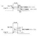
(トランジスタ回路)
先ず、本発明のトランジスタ回路の実施の形態について図1及び図2を参照して説明する。図1は、本実施の形態におけるトランジスタ回路の回路図であり、図2(A)及び(B)は夫々、該トランジスタ回路における各種信号のタイミング及び電圧を示したタイミングチャートである。
【0041】
図1において、トランジスタ回路100は、駆動用TFT110(Pチャネル型)、補償用TFT120(Pチャネル型)、リセット用TFT130(Nチャネル型)及びスイッチング用TFT140(Nチャネル型)を備えて構成されている。以下各トランジスタの構成について順に説明する。
【0042】
先ず、駆動用トランジスタの一例を構成する駆動用TFT110は、スイッチング用TFT140及び補償用TFT120を介して供給される入力信号に基づいてゲート111に印加されるゲート電圧Vgに応じて、ソース112及びドレイン113間のコンダクタンスが制御されるように構成されている。
【0043】
補償用トランジスタの一例を構成する補償用TFT120は、ゲート121がソース122及びドレイン123の一方(図1では、ドレイン123)に接続されている。即ち、補償用TFT120は所謂ダイオード接続されている。そして、補償用トランジスタ120は、ソース122及びドレイン123を介して、入力信号がゲート111に供給されるように且つコンダクタンスを高める方向に(図1では、ドレイン123の側が)ゲート111に接続されている。
【0044】
リセット手段の一例を構成するリセット用TFT130は、ソース132及びドレイン133の一方(図1では、ドレイン133)がゲート111に接続されており、ゲート131にリセットタイミング信号の一例としての電圧Vrscanのリセット走査信号(以下、リセット走査信号Vrscanと称す)が入力信号Vsigの供給前に供給された時に、ソース132及びドレイン133を介して電圧Vrsigのリセット信号(以下、リセット信号Vrsigと称す)をゲート111に供給するように構成されている。
【0045】
また、スイッチングトランジスタの一例を構成するスイッチング用TFT140は、ゲート141にスイッチングタイミング信号の一例としての電圧Vscanの走査信号(以下、走査信号Vscanと称す)が供給された時に、電圧Vsigの入力信号(以下、入力信号Vsigと称す)をソース142及びドレイン143を介して補償用TFT120に供給するように入力信号源及び補償用TFT120の間に接続されている。
【0046】
そして、駆動用トランジスタ110のソース112には、EL素子等の電流制御型(電流駆動型)素子500の一端が接続されており、この電流制御型素子500の他端には、所定電位の負電源−Vcが接続されている。また、駆動用トランジスタ110のドレイン113には、所定電位の正電源+Vcが接続されている。従って、駆動用トランジスタ110においてソース112及びドレイン113間のコンダクタンス制御が行われると、電流制御型素子500を流れる駆動電流Idが制御される(即ち、コンダクタンス変化に応じて駆動電流Idが変化する)。
【0047】
更に、駆動用トランジスタ110のゲート111には、保持容量160が接続されている。このため、一旦印加されたゲート電圧Vgは、保持容量160により保持される。
【0048】
次に、以上のように構成されたトランジスタ回路100の動作について図1と共に図2及び図3を参照して説明する。
【0049】
図2(A)に示すように、リセット走査信号Vrscanがリセット用TFT130に入力されると、リセット用TFT130が導通状態とされて、駆動用TFT110のゲート111には、リセット信号Vrsigが供給されて、ゲート111のゲート電圧Vgは、このリセット信号Vrsigの電圧Vrsigにほぼ等しいレベルとされる。この結果、入力信号Vsigの電圧Vsigの大小によらずに駆動用TFT110のゲート電圧Vgをリセット走査信号Vrsigの供給タイミングで一定電圧(即ち、電圧Vrsig)にリセットすることができる。
【0050】
そして、このリセット期間が終わり、走査信号Vscanがスイッチング用TFT140に供給されると、スイッチング用TFT140が導通状態とされて、駆動用TFT110のゲート111には、補償用TFT120を介してデータ信号Vsigが供給される。ここで、本実施の形態では特に補償用TFT120においてゲート121がドレイン123に接続されているため(即ち、ダイオード接続されているため)、負電圧をゲート111に印加することで道通状態とされるPチャネル型TFTである駆動用TFT110におけるゲート電圧Vgは、データ信号Vsigの電圧Vsigよりも補償用TFT120のしきい値電圧Vth2だけ負電圧側に降圧される。そして、このように降圧されたゲート電圧Vgは、走査信号Vscanや入力信号Vsigの供給停止後も、保持容量160により駆動期間中保持される。
【0051】
尚、リセット期間としては、ゲート電圧Vgがリセット信号Vrsigの電圧Vrsigとなる時間だけとれば十分である。このため、駆動期間をリセット期間よりも遥かに長く設定することができ、これにより、リセット期間中に駆動用TFT110がリセット信号Vrsigにより道通状態とされても、この間に駆動用TFT110のソース112及びドレイン113を介して流れる電流の駆動電流Idに対する影響を、無視できる程度に小さくできる。
【0052】
以上のように本実施の形態によれば、補償用TFT120のしきい値電圧Vth2の分だけ入力信号Vsigに対するゲート電圧Vgを降圧できるので、補償用TFT120がない場合と比較して、より低い入力信号Vsigの電圧Vsigを用いて同等のコンダクタンス制御を駆動用TFT110において行うことが可能となる。
【0053】
尚、図2(B)は、駆動用TFT110及び補償用TFT120を共にNチャネル型TFTから構成した場合のタイミングチャートであり、この場合には、正電圧をゲート111に印加することで道通状態とされるNチャネル型TFTである駆動用TFT110におけるゲート電圧Vgは、リセット時にリセット信号Vrsigの電圧Vrsigとされた後、入力信号Vsigの電圧Vsigよりも補償用TFT120のしきい値電圧Vth2だけ正電圧側に昇圧される。
【0054】
ここで、補償用TFT120を介することなく駆動用TFT110に入力信号Vsigを直接入力したとすると、即ち入力信号Vsigの電圧Vsigとゲート電圧Vgとが一致する場合には、図3(A)(これは駆動用TFT110がNチャネルの場合である)に示すように、駆動電流Idは、駆動用TFT110のしきい値電圧Vth1から立ち上がる特性を持つ。例えば、このしきい値電圧Vth1の設計基準値を2Vとすればしきい値のばらつきは±数V程度となる。そして、駆動用TFT110におけるしきい値電圧Vth1のばらつきがそのまま駆動電流Idのばらつきとして現われる。
【0055】
これに対し、本実施の形態では、補償用TFT120を介して駆動用TFT110に入力信号Vsigを入力するため、即ち入力信号Vsigの電圧Vsigを補償用TFT120のしきい値電圧Vth2の分だけ昇圧してゲート電圧Vgとする場合には、図3(B)(これは駆動用TFT110及び補償用TFT120が共にNチャネルの場合である)に示すように、補償用TFT120のしきい値電圧Vth2と駆動用TFT110のしきい値電圧Vth1とが相殺されて、トランジスタ回路100全体に対する入力信号Vsigのしきい値電圧Vthは零に近付くのである。そして、特に両しきい値電圧Vth1とVth2とがほぼ一致する場合には、このしきい値電圧Vthは、ほぼ零となる。このように、しきい値電圧Vth1とVth2とを一致させることは、例えば同一半導体基板上の近接位置に駆動用TFT110と補償用TFT120とを同型TFTから構成することにより比較的簡単にできる。このように構成すれば、両方のTFTにおける、薄膜形成されるゲート絶縁膜、半導体膜等の膜厚や、チャネル長等の各構成要素の平面形状や、チャネル形成用領域、ソース領域、ドレイン領域における不純物濃度や、動作時の温度状態などを容易に一致させることができるので、結局、両方のTFTのしきい値電圧Vth1とVth2とを完全に又はほぼ完全に一致させることが出来るのである。尚、しきい値特性を近似させる上では、チャネル長さは同じにする方が良いが、チャネル幅は同じでなくても良い。
【0056】
このように本実施の形態によれば、駆動用TFT110と補償用TFT120のしきい値特性や電圧電流特性を近付けることにより(理想的には一致させることにより)、駆動電流Idに対する入力信号Vsigのしきい値電圧Vthを零に近付ける(理想的には零に一致させる)ことが可能となる。
【0057】
更に、図3(A)及び図3(B)から判るように、複数のトランジスタ回路100を製造する場合に、各駆動用TFT110におけるしきい値電圧Vth1が相互にばらついたとしても、このしきい値電圧Vth1の大小によらずに、各補償用TFT120の作用により各トランジスタ回路100のしきい値電圧Vthは、零に近い値とされる。即ち、しきい値電圧Vthが一定の多数のトランジスタ回路100を製造できることになる。これは、後述のように多数のトランジスタ回路100間におけるしきい値電圧Vthのばらつきが問題となるような表示パネル用等の用途には特に役立つ。そして、各トランジスタ回路100において、相互に近接配置される一対の駆動用TFT110のしきい値電圧Vth1と補償用TFT120のしきい値電圧Vth2とを一致させることは、距離を隔てて別個に配置される二つの駆動用TFT110のしきい値電圧Vth1を一致させることよりも前述のように遥かに容易であるため、このように補償用TFT120により各トランジスタ回路100におけるしきい値電圧Vth1を補償する構成は、複数のトランジスタ回路100相互間のしきい値電圧Vthのばらつきを低減させるためには極めて効果的であると言える。
【0058】
以上のように本実施の形態によれば、トランジスタ回路100を複数作成する際に、しきい値電圧Vth1の相異なる複数の駆動用TFT110、即ち設計基準値としてのしきい値電圧(例えば、2.5V)から大きくばらついたしきい値電圧Vth1を夫々持つ複数の駆動用TFT110を用いたとしても、しきい値電圧Vthのばらつきが殆ど又は全くない複数のトランジスタ回路100を得ることが可能となる。このため、電流電圧特性についてTFTに要求される条件が緩くなり、歩留まりの向上及び製造コストの低減を図ることができる。
【0059】
尚、図3(A)及び図3(B)から判るように、しきい値電圧Vth1及びVth2を一致させることにより、各駆動用TFT110におけるコンダクタンス制御を入力信号Vsigの電圧Vsigよりも高いゲート電圧Vgを用いて行えるという第1の効果、及び複数のトランジスタ回路100間におけるしきい値電圧Vthのばらつきを低減するという第2の効果は、顕著に発揮されるが、各トランジスタ回路100において駆動用TFT110のしきい値電圧Vth1と補償用TFT120のしきい値電圧Vth2とを完全に一致させなくとも、両しきい値電圧は相殺しあう性質をもつので、両しきい値電圧の類似性に応じた程度でこれらの第1及び第2の効果は発揮される。
【0060】
本実施の形態では特に、ゲート111に対し入力信号Vsigに応じて制御されるコンダクタンスの最高値よりも高いコンダクタンスの値に対応する電圧を有するリセット信号Vrsigを供給するように構成されている。従って、入力信号Vsigの電圧値Vsigの大小によらずにリセット後に、このコンダクタンスを高める方向でゲート111が接続された補償用TFT120を介して入力信号Vsigをゲート111に供給することが可能となる。しかも本実施の形態では、リセット信号Vrsigは、入力信号Vsigの最大電圧よりも補償用TFT120のしきい値電圧Vth2分以上大きい電圧に設定されている。従って、リセット後に入力信号Vsigが入力されると、入力信号Vsigの電圧Vsigの大小や補償用TFT120のしきい値電圧Vth2の大小によらずに常に、その入力信号Vsigの電圧Vsigよりも補償用TFT120のしきい値電圧Vth2分だけ高い電圧を、ゲート111に供給することが出来るのである。
【0061】
尚、従来の液晶表示素子で良く用いられている、入力信号Vsigの反転が行われる場合には、反転した入力信号も含めた全ての入力信号Vsigに対しても、上記のリセット信号Vsigの関係が成り立つことが望ましい。
【0062】
このリセット信号Vrsigの電圧設定による効果について図4及び図5を参照して検討を加える。ここで、図4は、しきい値の設計基準値を例えば−2.5Vとしてその基準値からのしきい値電圧のばらつきΔVthに対する駆動電流Idの変化を、(1)補償用TFT120無しで駆動用TFT110に直接入力信号Vsigを供給した場合(特性曲線C1)、(2)リセット信号Vrsigを5Vとして補償用TFT120を介して駆動用TFT110に入力信号Vsigを供給した場合(特性曲線C2)、及び(3)リセット信号Vrsigを0Vとして補償用TFT120を介して駆動用TFT110に入力信号Vsigを供給した場合(特性曲線C3)について夫々示したものである。また、図5(A)は、特性曲線C2に対応するゲート電圧Vgの変動範囲を示し、図5(B)は、特性曲線C3に対応するゲート電圧Vgの変動範囲を示す。なお、ここで、Vsig=7.5V、+Vc=10V、−Vc=5Vとしている。
【0063】
図4において、特性曲線C1で示したように、補償用TFT120無しの場合には、しきい値電圧のばらつきΔVthが、そのまま駆動電流Idのばらつきとして顕著に現われている。
【0064】
特性曲線C2で示したように、リセット信号Vrsigを5Vとして補償用TFTを用いた場合には、しきい値電圧のばらつきΔVthが、プラス側ではかなり補償されているが、マイナス側では、駆動電流Idのばらつきとして現われている。これは、図5(A)に示すようにマイナス側では、リセット後に入力信号Vsigが入力されたとき、ゲート電圧Vgを、入力信号Vsigよりも、しきい値電圧Vth2の分だけ負電圧側に降圧する(補償する)ことができないためである。何故なら、ダイオードである補償用TFT120は、ゲート電圧Vgをリセット信号Vrsigから入力信号Vsigへ近付けることは出来ても遠ざけることは出来ないからである。
【0065】
また、特性曲線C3で示したように、リセット信号Vrsigを0Vとして補償用TFTを用いた場合には、しきい値電圧のばらつきΔVthが、駆動電流Idのばらつきとして殆ど現われていない。これは、図5(B)に示すように、リセット後に入力信号Vsigが入力されたとき、ゲート電圧Vgを、入力信号Vsigよりも、しきい値電圧Vthの分だけ負電圧側に降圧する(補償する)ことができるためである。なお、ここで与えたVsig=7.5Vは、入力信号Vsigの最小電位だと考えれば、全てのVsigに対して補償できるかということに対して、上記考察が成り立つ。
【0066】
以上のように本実施の形態では、入力電圧Vsigの大小や補償用TFT110のしきい値電圧Vth2の大小によらずに常に、その入力信号Vsigの電圧よりも補償用TFT120のしきい値電圧Vth2分だけ低い電圧Vgを、駆動用TFT110のゲート111に印加することが出来るのである。
【0067】
尚、図2(A)及び図2(B)において、ゲート電圧Vgは駆動期間中、保持容量160により保持される。このため、保持容量160により、複数のトランジスタ回路100間におけるゲート電圧Vgの保持特性のばらつきをも低減(補償)することができる。
【0068】
以上図1から図5を用いて説明したように、本実施の形態のトランジスタ回路100によれば、EL素子等の電流制御型素子500を比較的低電圧の入力信号Vsigで電流駆動することが可能となり、しかも、複数の駆動用TFT110間における電流電圧特性やしきい値特性のばらつきによらずに、複数の電流制御型素子500を入力信号Vsigの電圧に応じて精度良く電流制御するができる。
【0069】
尚、図1に示した例では、Pチャネル型TFTとNチャネル型TFTとを混ぜて構成しているが、全てのTFTをNチャネル型TFTから構成してもよいし、或いは、全てのTFTをPチャネル型TFTから構成してもよい。但し、駆動用TFT110の電流電圧特性やしきい値特性を補償用TFT120で補償する観点からは、これらの駆動用TFT110及び補償用TFT120を同一工程により同型のTFTとして構成した方が有利である。特に、両TFTを同一薄膜形成工程で形成すれば、両TFT間の特性類似の度合いは一般に増すため、電流電圧特性やしきい値特性のばらつきが全く又は殆どないトランジスタ回路100を同一基板上で得ることが可能となる。他方、リセット用TFT130やスイッチング用TFT140は、駆動用TFT110がPチャネル型であるかNチャネル型であるかによらず、Pチャネル型でもNチャネル型でも構わない。但し、全てのTFTを同型のTFTとした方が製造上有利であることも多い。
【0070】
また、本実施の形態における各種のTFT110〜140を、接合型、並列・直列接続等のいずれの種類の電界効果トランジスタ(FET)から構成してもよい。
【0071】
更に、図6に示すように、上述の如きトランジスタ回路をバイポーラトランジスタから構成してもよい。この場合、上述のゲート、ソース及びドレインをベース、エミッタ及びコレクタに夫々対応させて、バイポーラトランジスタから駆動用トランジスタ110’を構成すると共にバイポーラトランジスタから補償用トランジスタ120’を構成して、トランジスタ回路100’とすればよい。一般にバイポーラトランジスタの場合には、しきい値電圧は、例えば0.7Vを中心として、そのばらつきはTFTと比較すると小さいが、このように構成しても、駆動用トランジスタ110’における電流電圧特性やしきい値特性のばらつきが駆動電流Idに及ぼす影響を補償用トランジスタ120’により補償することが出来る。更に、比較的低電圧で駆動用トランジスタ110’による駆動を行うことが出来る。特に、駆動用トランジスタ110’と補償用トランジスタ120’とを同一製造工程で製造すれば、これら両トランジスタ間の特性類似の度合いは一般に増すため、電流電圧特性やしきい値特性のばらつきが殆ど無い又は低減された多数のトランジスタ回路100’を得ることが可能となる。
【0072】
以上の実施の形態における電流制御型素子500としては、有機EL素子、無機EL素子等の電流制御型発光素子、電流制御型の熱転写素子など各種の素子が挙げられる。
【0073】
(表示パネル)
本発明の表示パネルの実施の形態について図7から図10を参照して説明する。図7は、表示パネルの全体構成を示すブロック図であり、図8は、表示パネルにおける一つの画素部の平面図であり、図9(A)、図9(B)及び図9(C)は夫々、そのA−A’断面図、B−B’断面図及びC−C’断面図であり、図10は、相隣接する4つの画素部の回路図である。
【0074】
本実施の形態における表示パネルは、上述した本発明のトランジスタ回路を夫々含むと共にマトリクス状に配置された複数の画素部を備えており、該複数の画素部には、電流制御型発光素子の一例としてEL素子50が夫々設けられて構成されている。
【0075】
図7に示すように、表示パネル200は、TFTアレイ基板1を有し、該TFTアレイ基板1上において複数の画素部2がマトリクス状に配置された画面表示領域には、Y方向に夫々伸びておりX方向に配列された複数のデータ線11と、X方向に夫々伸びておりY方向に配列された複数の走査線12と、複数のデータ線11と平行に並べられた複数の共通給電線13とを備えている。表示パネル1は更に、画面表示領域の周囲に、各データ線11にデータ信号を供給するデータ線駆動回路21と、各走査線12に走査信号を供給する一対の走査線駆動回路22と、各画素部2における道通不良、絶縁不良、素子の欠陥等を検査するための検査回路23とを備えて構成されている。なお、本実施の形態では、各駆動回路は、TFTアレイ基板1上に画素部2と共通の工程で形成されているが、TFTアレイ基板1上にない回路とされてもよいし、又は画素部2と別の工程で形成されてもよい。
【0076】
図8に示すように、各画素部2には、図1から図6を用いて説明した駆動用TFT110、補償用TFT120、リセット用TFT130、スイッチング用TFT140及び保持容量160が設けられている。そして、前段の走査線12bが図1におけるリセット走査信号Vrscan用の配線となり、当段の走査線12aが図1における走査信号Vscan用の配線及びリセット信号Vrsig用の配線となり、当段のデータ線11aが図1における入力信号Vsig(データ信号)用の配線となっている。更に、共通給電線13が正電源+Vに接続されており、EL素子50が駆動用TFT110と後述の対向電極との間に接続されており、該対向電極が負電源−Vに接続されている。
【0077】
図9(A)に示すように、スイッチング用TFT140、補償用TFT120及び保持容量160は、図8のA−A’断面に沿って、TFTアレイ基板上1に半導体膜(ポリシリコン膜)4、酸化シリコン膜や窒化シリコン膜からなるゲート絶縁膜5、Ta(タンタル)膜6、酸化シリコン膜や窒化シリコン膜からなる第1層間絶縁膜7及びAl膜8から構成されている。尚、ゲート電極形成用のTa膜6の代わりに、低抵抗ポリシリコン膜を成膜してもよい。
【0078】
より具体的には、スイッチング用TFT140は、ポリシリコン膜6からなるゲート141を持つトップゲート型のTFTであり、ゲート絶縁膜5を介してゲート141に対向する半導体層4部分をチャネル形成用領域として、その両側にn型に高濃度ドープされたソース142及びドレイン143を備えたNチャネル型のTFTとして構成されている。そして、ソース142は、ゲート絶縁膜5及び第1層間絶縁膜7に開孔されたコンタクトホールを介してAl膜8からなるデータ線11aに接続されている。また、ドレイン143は、ゲート絶縁膜5及び第1層間絶縁膜7に開孔されたコンタクトホール及びAl膜8を中継して、補償用TFT120に接続されている。
【0079】
補償用TFT120は、Ta膜6からなるゲート121を持つトップゲート型のTFTであり、ゲート絶縁膜5を介してゲート121に対向する半導体膜4部分をチャネル形成用領域として、その両側にp型に高濃度ドープされたソース122及びドレイン123を備えたPチャネル型のTFTとして構成されている。そして、ゲート絶縁膜5及び第1層間絶縁膜7に開孔されたコンタクトホール及びAl膜8を中継してスイッチング用TFT140及び保持容量160並びに駆動用TFT110のゲート111に接続されている。
【0080】
また、保持容量160は、2重のコンデンサ構成を有するように、半導体膜4、Ta膜6及びAl膜8が、ゲート絶縁膜5及び第1層間絶縁膜7を介して対向配置されて構成されている。そして保持容量を構成する半導体膜4部分は、ゲート絶縁膜5及び第1層間絶縁膜7に開孔されたコンタクトホールを介してAl膜8に接続されており、保持容量を構成するTa膜6部分は、第1層間絶縁膜7に開孔されたコンタクトホールを介してAl膜8に接続されている。
【0081】
図9(B)に示すように、リセット用TFT130は、図8のB−B’断面に沿って、TFTアレイ基板上1に半導体膜4、ゲート絶縁膜5、Ta膜6、第1層間絶縁膜7及びAl膜8から構成されている。
【0082】
より具体的には、リセット用TFT130は、Ta膜6からなるゲート131を持つトップゲート型のTFTであり、ゲート絶縁膜5を介してゲート131に対向する半導体層4部分をチャネル形成用領域として、その両側にn型に高濃度ドープされたソース132及びドレイン133を備えたNチャネル型のTFTとして構成されている。そしてソース132及びドレイン133は、ゲート絶縁膜5及び第1層間絶縁膜7に開孔されたコンタクトホール及びAl膜8を中継して、Ta膜6からなる当段の走査線12a及び駆動用TFT110のゲート111に夫々接続されている。
【0083】
また、図9(C)に示すように、駆動用TFT110は、図8のC−C’断面に沿って、TFTアレイ基板上1に半導体膜4、ゲート絶縁膜5、Ta膜6、第1層間絶縁膜7及びAl膜8から構成されている。そして、第2層間絶縁膜9上には、駆動用TFT110のドレイン113にコンタクトホール及びAl膜8を中継して接続されたITO膜51が形成され、その上にEL素子50が形成されている。他方、駆動用TFT110のソース112は、コンタクトホールを介してAl膜8からなる共通給電線13に接続されている。また、相隣接する画素部2におけるEL素子50は、電気絶縁性のバンク52により相隔てられている。好ましくは、バンク52は遮光性を持つものがよい。バンク52は、例えば、遮光性のレジストからなり、当該表示パネル200の画面表示領域の周囲を覆う周辺見切り領域にもバンク52を設けるようにしてもよい。そして、EL素子50上には、Al等の低抵抗金属或いはITO等からなる対向電極(上電極)56が設けられている。
【0084】
図10に示すように、表示パネル200においては特に、共通給電線13によりX方向に相隣接した画素部2の双方に対して正電源+Vが供給される構成を採り、正電源+V供給用の電源配線を単純に画素部2の列毎に設ける場合と比較して、電源配線の数を約1/2にしている。また、リセット用TFT130のゲート131に入力されるリセット走査信号Vrscanを前段の走査線12bにより供給し、リセット用TFT130に入力されるリセット信号Vrsigを当段の走査線12bにより供給する構成を採ることにより、リセット走査信号Vrscan専用の配線やリセット信号Vrsig専用の配線を設ける場合と比較して信号配線の数を減らしている。このように電源配線数や信号配線数を増やさないようにすることにより、従来の表示パネルには設けられていない補償用TFT120やリセット用TFT130を設けるスペースを確保することができる。勿論、本実施の形態と違って、各画素毎に共通給電線を設けて、各画素毎にパターンを同じにしたものや、リセット走査信号Vrscan専用の配線や、リセット信号Vrsig専用の配線を設けたものに対しても、本発明の思想は適用できる。
【0085】
尚、本実施の形態のように電流駆動型発光素子であるEL素子50を用いた表示パネル200の場合には、例えば、液晶パネルのように画素の開口領域を増やさなくても、発光素子に供給する電流量を増加させればこれに応じて自発光するが故に、画像表示に必要な明るさを得ることができる。従って、本実施の形態のように、配線の占める領域を節約して各種のTFTを画素部2に形成するスペースを確保してもよいし、各EL素子50の大きさを小さくすることにより各種のTFTを画素部2に形成するスペースを確保してもよい。
【0086】
次に、本実施の形態の表示パネル200の動作について図7及び図10を参照して説明する。
【0087】
走査線駆動回路22から前段の走査線12bに走査信号Vscanが供給されると、これが当段のリセット走査信号Vrscanとして、当段のリセット用TFT130のゲート131に入力される。これと並行して、走査線駆動回路22から当段の走査線12aにリセット信号Vrsigが供給されて、当段の駆動用TFT110のゲート電圧Vgは、リセット信号Vrsigの電位とされる(図2(A)参照)。このとき、リセット信号Vrsigは、走査信号Vscanのオフ電位と同一でもかまわない。続いて、走査線駆動回路22から当段の走査線12aに走査信号Vscanが供給されると、これが当段のスイッチング用TFT140のゲート141に入力される。これと並行して、データ線駆動回路21から当段のデータ線11aに入力信号Vsig(データ信号)が供給されて、スイッチング用TFT140及び補償用TFT120を介して、この電圧Vsigが補償用TFT120のしきい値電圧Vth2分だけ降圧されて、当段の駆動用TFT110のゲート111に、ゲート電圧Vgとして供給される(図2(A)参照)。この結果、この降圧されたゲート電圧Vgに応じて、駆動用TFT110のソース112及びドレイン113間のコンダクタンスが制御されて、正電源+V及び負電源−Vの間で、EL素子50を流れる駆動電流Idが制御される。
【0088】
従って、各画素部2に設けられた駆動用TFT110におけるしきい値電圧Vth1のばらつきが補償用TFT120のしきい値Vth2により補償されて、複数の画素部2間における駆動電流Idに対するデータ信号Vsigのしきい値のばらつきが殆どなくなり、表示パネル200の画面表示領域全体にわたって均一の明るさでむらのない画像表示が可能とされる。また、補償用TFT120による降圧作用により比較的小さい電圧のデータ信号Vsigを用いて駆動電流Idを制御することも可能とされる。
【0089】
以上の実施の形態では、リセット用TFT130によりゲート電圧Vgを入力信号Vsigの供給前にリセットしているが、例えば、静止画を表示する期間には、同じ入力信号Vsigにより複数フレームに亘って駆動電流Idの制御を行えばよいので、係るリセット動作を各走査毎に行う必要はない。また、このように電気的なリセット信号Vrsigの代わりに光照射によりゲート電圧Vgをリセットする(所定のリセット電圧にする)ように構成してもよい。更にまた、リセット用TFT130の代わりにスイッチング用TFT140や補償用TFT120を介してリセット信号Vrsigを供給するように構成してもよい。他方、アクティブマトリクス駆動の如くスイッチングを行わない用途であれば、スイッチング用TFT140やスイッチング動作が不要なことは言うまでもない。
【0090】
(電子機器)
次に、以上詳細に説明した表示パネル200を備えた電子機器の実施の形態について図11から図13を参照して説明する。
【0091】
先ず図11に、このように表示パネル200を備えた電子機器の概略構成を示す。
【0092】
図11において、電子機器は、表示情報出力源1000、表示情報処理回路1002、駆動回路1004、表示パネル1006、クロック発生回路1008並びに電源回路1010を備えて構成されている。
【0093】
前述した実施の形態における表示パネル200は、本実施の形態における表示パネル1006及び駆動回路1004に相当する。従って、表示パネル1006を構成するTFTアレイ基板の上に、駆動回路1004を搭載してもよく、更に表示情報処理回路1002等を搭載してもよい。或いは、表示パネル1006を搭載するTFTアレイ基板に対し駆動回路1004を外付けして構成してもよい。
【0094】
表示情報出力源1000は、ROM(Read Only Memory)、RAM(Random Access Memory)、光ディスク装置などのメモリ、テレビ信号を同調して出力する同調回路等を含み、クロック発生回路1008からのクロック信号に基づいて、所定フォーマットの画像信号などの表示情報を表示情報処理回路1002に出力する。表示情報処理回路1002は、増幅・極性反転回路、相展開回路、ローテーション回路、ガンマ補正回路、クランプ回路等の周知の各種処理回路を含んで構成されており、クロック信号に基づいて入力された表示情報からデジタル信号を順次生成し、クロック信号CLKと共に駆動回路1004に出力する。駆動回路1004は、表示パネル200を駆動する。電源回路1010は、上述の各回路に所定電源を供給する。
【0095】
次に図12から図13に、このように構成された電子機器の具体例を夫々示す。
【0096】
図12において、電子機器の他の例たるマルチメディア対応のラップトップ型のパーソナルコンピュータ(PC)1200は、上述した表示パネル200がトップカバーケース1206内に備えられており、更にCPU、メモリ、モデム等を収容すると共にキーボード1202が組み込まれた本体1204を備えている。
【0097】
また図13に示すように、駆動回路1004や表示情報処理回路1002を搭載しない表示パネル1304の場合には、駆動回路1004や表示情報処理回路1002を含むIC1324がポリイミドテープ1322上に実装されたTCP(Tape Carrier Package)1320に、TFTアレイ基板1の周辺部に設けられた異方性導電フィルムを介して物理的且つ電気的に接続して、表示パネルとして、生産、販売、使用等することも可能である。
【0098】
以上図12から図13を参照して説明した電子機器の他にも、テレビ、ビューファインダ型又はモニタ直視型のビデオテープレコーダ、カーナビゲーション装置、電子手帳、電卓、ワードプロセッサ、エンジニアリング・ワークステーション(EWS)、携帯電話、テレビ電話、POS端末、タッチパネルを備えた装置等などが図11に示した電子機器の例として挙げられる。
【0099】
以上説明したように、本実施の形態によれば、表示パネルの全面に渡って明るさのむらが少なく且つ比較的低電圧で駆動することも可能な各種の電子機器を実現できる。
【0100】
【発明の効果】
本発明のトランジスタ回路によれば、補償用トランジスタのしきい値電圧の分だけ入力信号の電圧に対してゲート電圧を降圧もしくは昇圧できるので、低い入力信号の電圧により駆動用トランジスタにおけるコンダクタンス制御を行うことができる。更に、補償用トランジスタと駆動用トランジスタとのしきい値特性や電圧電流特性を近付けることにより、駆動電流に対する入力信号のしきい値電圧を零に近付けることも可能となる。更にまた、複数のしきい値特性の相異なる駆動用トランジスタを用いて当該トランジスタ回路を複数作成した場合に、複数のしきい値電圧の異なる複数の駆動用トランジスタ、即ち設計基準値から大きくばらついたしきい値電圧を夫々持つ複数の駆動用トランジスタを用いたとしても、複数のトランジスタ回路におけるしきい値電圧のばらつきが殆ど又は全くない複数のトランジスタ回路を得ることも可能となる。
【0101】
本発明の表示パネルによれば、明るさむらが低減された画像表示を低電圧の入力信号を用いて実現できる。
【0102】
また、本発明の電子機器によれば、高品位の画像表示が可能な、パーソナルコンピュータ、ページャ等の様々な電子機器を実現可能となる。
【図面の簡単な説明】
【図1】トランジスタ回路の一実施の形態における回路図である。
【図2】図1のトランジスタ回路における各種信号のタイミングチャート(図2(A))、及び図1のトランジスタ回路の変形例における各種信号のタイミングチャート(図2(B))である。
【図3】駆動用TFTを備えた比較例におけるしきい値特性を示す特性図(図3(A))、及び補償用TFTと駆動用TFTとを備えた本実施の形態におけるしきい値特性を示す特性図(図3(B))である。
【図4】しきい値のばらつきΔVthに対する駆動電流Idの変化を各種の場合について示す特性図である。
【図5】本実施の形態においてリセット信号Vrsigを5Vにした場合の補償用TFTによる降圧作用を示すタイミングチャート(図5(A))、及びリセット信号Vrsigを0Vにした場合の補償用TFTによる降圧作用を示すタイミングチャート(図5(B))である。
【図6】トランジスタ回路の他の実施の形態における回路図である。
【図7】表示パネルの実施の形態の全体構成を示す平面図である。
【図8】図7の表示パネルの一画素部の平面図である。
【図9】図8のA−A’断面図(図9(A))、B−B’断面図(図9(B))及びC−C’断面図(図9(C))である。
【図10】図7の表示パネルにおける相隣接する4つの画素部の回路図である。
【図11】本発明による電子機器の実施の形態の概略構成を示すブロック図である。
【図12】電子機器の一例としてのパーソナルコンピュータを示す正面図である。
【図13】電子機器の他の例としてのTCPを用いた液晶装置を示す斜視図である。
【符号の説明】
1…TFTアレイ基板
2…画素部
11…データ線
12…走査線
13…共通給電線
21…データ線駆動回路
22…走査線駆動回路
23…検査回路
50…EL素子
100…トランジスタ回路
110…駆動用TFT
120…補償用TFT
130…リセット用TFT
140…スイッチング用TFT
160…保持容量[0001]
BACKGROUND OF THE INVENTION
The present invention belongs to a technical field of a transistor circuit including a plurality of transistors such as a thin film transistor (hereinafter referred to as TFT), a field effect transistor, and a bipolar transistor, and in particular, a source and a drain according to a voltage supplied to a gate. Transistor circuit comprising a driving transistor for controlling a driving current supplied to a driven element such as a current control type (current driving type) element via the source and drain by controlling the conductance between them Belongs to the technical field.
[0002]
[Prior art]
In general, a transistor has a voltage-current characteristic and a threshold value depending on various conditions such as a semiconductor film quality, film thickness, impurity concentration, diffusion region, gate insulating film quality, film thickness, operating temperature, etc. Variations occur in greater or lesser amounts. In the case of a bipolar transistor using crystal silicon, such a variation in threshold value is relatively small, but in the case of a TFT, such a variation is usually large. In particular, in the case of a large number of TFTs formed over a wide range on a TFT array substrate in a display panel such as a liquid crystal panel or an EL panel, such a variation in current-voltage characteristics and threshold values becomes very large. There are many. For example, even if this type of TFT is manufactured so that the threshold value is about 2V (volt) (+ 2V for N channel, -2V for P channel), the variation may be about ± several volts.
[0003]
Here, in the case of a voltage control (voltage drive) method for controlling the voltage of a pixel portion made of a liquid crystal or the like as in the case of a so-called TFT liquid crystal panel, the voltage-current characteristics in the driving TFT provided in each pixel portion It is relatively rare that variations in threshold value become a problem. In other words, in this case, even if there is some variation in the current-voltage characteristics and threshold value of the TFT, as long as a sufficient switching time is provided, the accuracy of the voltage supplied to each pixel unit from the outside via the TFT can be improved. This is because the display density and brightness in each pixel portion can be controlled with high accuracy by increasing the value. Therefore, even in display TFT liquid crystal panels and the like where display density and brightness unevenness in each pixel portion are regarded as important, high-quality images are obtained by using TFTs having relatively large variations in current-voltage characteristics and threshold values. Display and so on.
[0004]
On the other hand, in recent years, a display panel having a current-controlled light emitting element such as an organic EL that emits light so that brightness changes according to the amount of current supplied in a pixel portion has been developed, and uses a backlight or reflected light. Therefore, the display panel is attracting attention as a display panel that can display images without power consumption, has low power consumption, has little viewing angle dependency, and sometimes realizes bendability. Also in the case of this EL panel, a driving TFT is used in each pixel portion in order to perform active matrix driving. For example, the drive TFT drain is connected to the EL element through the hole injection electrode, and the drive is supplied to the EL element from the power supply wiring connected to the source in accordance with the voltage of the data signal applied to the gate. It is configured to control (change) the current. When the driving TFT is used in this way, the driving current flowing through the EL element is controlled by controlling the conductance between the source and the drain in accordance with the voltage change of the input signal, and the brightness (luminance) in each pixel portion. Can be changed, and an image can be displayed.
[0005]
[Problems to be solved by the invention]
However, particularly in the case of a current control type element such as the EL panel described above, variations in voltage-current characteristics and threshold values in the driving TFT provided in each pixel portion become a problem. That is, in this case, even if the voltage accuracy of the data signal supplied to the driving TFT from the outside is increased to some extent, variations in the voltage / current characteristics and threshold values in the driving TFT are regarded as variations in the driving current with respect to the data signal. Since it appears as it is, the accuracy of the drive current is reduced. As a result, the brightness in each pixel portion also varies according to variations in the threshold value of the driving TFT. In particular, in the current low-temperature polysilicon TFT manufacturing technology, such variations in voltage-current characteristics and threshold values occur to a considerable degree, and this problem is very large in practical use.
[0006]
In order to solve this problem, if each TFT is manufactured so as to reduce variations in voltage-current characteristics and threshold values, the yield is lowered, and in particular, a device configured using a large number of TFTs such as a display panel. In this case, the yield is drastically reduced, which is contrary to the general demand for cost reduction. Alternatively, it is almost impossible to manufacture a TFT that reduces such variations. In addition, even if a circuit for compensating for variations in current-voltage characteristics and threshold values in each TFT is separately provided, the device is still complicated and large, and the power consumption is increased. In an arrayed display panel, it is expected that the yield will decrease again, or it will be difficult to meet the recent demands for lower power consumption and smaller and lighter devices.
[0007]
The present invention has been made in view of the above-described problems, and is a transistor circuit that performs conductance control in a driving transistor in accordance with the voltage of an input signal, and the conductance can be controlled by a relatively low voltage input signal. In addition, a transistor circuit that can compensate for variations in current-voltage characteristics and threshold characteristics of a driving transistor by using a relatively small number of transistors with relatively small power consumption, and a display panel using the transistor circuit Another object is to provide an electronic device.
[0008]
[Means for Solving the Problems]
A current control element to which a current according to an input signal is supplied;
A driving transistor that is connected in series with the current-controlled element and whose conductance is controlled according to a voltage supplied to the gate, and the same type as the driving transistor, the gate is connected to the gate of the driving transistor, A compensation transistor having a gate connected to either the source or the drain so as to have a diode characteristic, and the threshold voltage of the compensation transistor is set to the conductance of the drive transistor with respect to the input signal. The input signal is supplied to the gate of the driving transistor via the compensation transistor so that a voltage applied in the direction of increasing the voltage is supplied to the gate of the driving transistor.
In addition, a current control type element to which a current according to an input signal is supplied and a current control type element connected in series with the current control type element to control a current supplied to the current control type element according to a voltage supplied to a gate. A channel-type driving transistor, and a P-channel type compensating transistor whose gate and drain are connected to the gate of the driving transistor, and the input signal is transmitted to the driving transistor via the compensating transistor. It is characterized by being supplied to the gate.
Further, the gate and source of the compensating transistor are arranged such that the threshold voltage of the driving transistor and the threshold voltage of the compensating transistor cancel each other with respect to the current flowing through the current control element. Alternatively, the drain is connected.
Further, the driving transistor and the compensating transistor are the same type transistors having the same channel length.
Further, the voltage based on the next input signal before the voltage based on the input signal is supplied to the gate of the driving transistor or after the voltage based on one input signal is supplied to the gate of the driving transistor. Before the gate is supplied to the gate, a reset transistor for supplying a reset signal to the gate of the driving transistor is provided.
Further, the transistor circuit according to the present invention may be arranged before the voltage based on the input signal is supplied to the gate of the driving transistor or after the voltage based on one input signal is supplied to the gate of the driving transistor. A reset transistor for supplying a reset signal to the gate of the driving transistor before a voltage based on the input signal is supplied to the gate.
Furthermore, the transistor circuit of the present invention is characterized in that the reset signal is a voltage corresponding to a conductance value higher than the highest conductance value of the driving transistor controlled by a voltage based on the input signal, or a maximum value of the input signal. The voltage is higher than the voltage by the threshold voltage of the compensation transistor.
Furthermore, the transistor circuit of the present invention is provided with a plurality of the transistor circuits in accordance with intersections of a plurality of scanning lines to which a scanning signal is supplied and a plurality of data lines to which the input signal is supplied. The scanning signal may be supplied to a gate to be in a conductive state, and may further include a switching transistor that supplies the input signal to the compensation transistor.
Furthermore, the transistor circuit of the present invention is characterized in that the current control element is a light emitting element.
In addition, the display panel includes a plurality of scanning lines to which scanning signals are supplied, a plurality of data lines to which input signals are supplied, and a plurality of pixel portions provided in accordance with intersections of the scanning lines and the data lines. Each of the pixel units includes a current control element that is supplied with a current corresponding to an input signal, and a drive that is connected in series with the current control element and whose conductance is controlled according to a voltage supplied to a gate. A compensation transistor having the same type as the driving transistor, a gate connected to the gate of the driving transistor, and a gate connected to either the source or the drain so as to have diode characteristics. A voltage obtained by adding a threshold voltage of the compensation transistor to the input signal in a direction to increase conductance of the driving transistor, Serial to supply to the gate of the driving transistor, the input signal is characterized by comprising supplied to the gate of the driving transistor through the compensating transistor.
In addition, the display panel includes a plurality of scanning lines to which scanning signals are supplied, a plurality of data lines to which input signals are supplied, and a plurality of pixel portions provided in accordance with intersections of the scanning lines and the data lines. Each of the pixel units includes a current control type element to which a current corresponding to the input signal is supplied, and the current control type element connected in series with the current control type element and according to a voltage supplied to a gate. A P-channel driving transistor for controlling the current supplied to the transistor, a P-channel compensating transistor whose gate and drain are connected to the gate of the driving transistor, and the scanning signal is supplied to the gate to be in a conductive state. A switching transistor for supplying the input signal to the compensation transistor, and the input signal is transmitted to the driving transistor via the compensation transistor. Characterized by comprising supplied to the gate of the register.
Further, in the display panel of the present invention, the threshold voltage of the driving transistor and the threshold voltage of the compensation transistor cancel each other with respect to the current flowing through the current control element. The gate of the compensation transistor and the source or drain are connected.
Furthermore, the display panel of the present invention is characterized in that the driving transistor and the compensating transistor are transistors of the same type with the same channel length.
Further, the display panel according to the present invention may be arranged before the voltage based on the input signal is supplied to the gate of the driving transistor or after the voltage based on one input signal is supplied to the gate of the driving transistor. A reset transistor for supplying a reset signal to the gate of the driving transistor before a voltage based on the input signal is supplied to the gate.
In the display panel of the present invention, the reset signal may be a voltage corresponding to a conductance value higher than the highest conductance value of the driving transistor controlled by a voltage based on the input signal, or a maximum value of the input signal. The voltage is higher than the voltage by the threshold voltage of the compensation transistor.
Furthermore, the display panel of the present invention is characterized in that the current control element is a light emitting element.
According to another aspect of the invention, an electronic apparatus includes the display panel.
[0009]
In addition, the transistor circuit according to the embodiment of the present invention includes a first gate, a first source, and a first drain, and the first source and the first according to the voltage of the input signal supplied to the first gate. A driving transistor in which conductance between the drains is controlled; a second gate, a second source, and a second drain; and the second gate is connected to one of the second source and the second drain; A compensation transistor connected to the first gate in a direction to increase the conductance so that the input signal is supplied to the first gate via a second source and a second drain; To do.
According to the transistor circuit, one of the second source and the second drain of the compensation transistor is connected to the first gate of the driving transistor, and the driving transistor is connected via the second source and the second drain. An input signal is supplied to the first gate. In the driving transistor, the conductance between the first source and the first drain is controlled according to the voltage of the input signal supplied to the first gate. Here, the compensation transistor has a second gate connected to the second drain, and is connected to the first gate in a direction of increasing conductance between the first source and the first drain. That is, the compensation transistor has a diode characteristic. For example, if the driving transistor is an N-channel type, it can be energized only in the direction from the first gate to the input signal source. Alternatively, if the driving transistor is a P-channel type, it can be energized in the direction from the input signal source to the first gate.
[0010]
For this reason, when the input signal is supplied to the transistor circuit, the gate voltage of the first gate is equal to the threshold value of the compensation transistor compared to the voltage of the input signal at the time of input to the compensation transistor. The voltage is boosted to the side where the conductance of the driving transistor is increased. Therefore, in order to obtain a desired conductance in the driving transistor, an input signal having a voltage lower than the gate voltage corresponding to the conductance by the threshold value (voltage) of the compensating transistor is supplied via the compensating transistor. You can do it. In this way, the gate voltage for the input signal can be boosted by the threshold value (voltage) of the compensation transistor, so that equivalent conductance control can be performed with a lower input signal voltage compared to the case without the compensation transistor. Can be done.
[0011]
In general, this input signal often has a higher frequency than other signals, and if a lower input signal is sufficient, a considerable reduction in power consumption can be expected.
[0012]
Further, the voltage of the input signal is boosted by the compensating transistor to the gate voltage at the first gate in this way through the source and drain whose conductance is controlled in the driving transistor when viewed as the entire transistor circuit. The threshold value of the input signal relative to the flowing drive current is lowered from the threshold voltage of the driving transistor by the threshold voltage of the compensation transistor, which is a boost from the input voltage to the gate voltage. That is, in the threshold value of the input voltage with respect to the drive current, the threshold value of the compensation transistor and the threshold value of the drive transistor are offset. Therefore, the threshold value of the input signal with respect to the drive current can be brought close to zero by bringing the threshold characteristics and voltage-current characteristics of the two closer.
[0013]
Furthermore, by canceling out the threshold value of the driving transistor and the threshold value of the compensating transistor in the entire transistor circuit in this way, the transistor circuit is independent of the magnitude of the threshold value of the driving transistor. The threshold value of the input signal as a whole can be brought close to a certain value (zero). That is, when a plurality of transistor circuits are formed using a plurality of driving transistors having different threshold values, the threshold values of the driving transistor and the compensating transistor in each transistor circuit are close to each other (ideal If the two are matched, the threshold difference between the transistor circuits is smaller than the threshold difference between the driving transistors (ideally, the difference is almost eliminated). ). Therefore, when creating a plurality of transistor circuits, it is possible to obtain a plurality of transistor circuits with little or no threshold variation even when a plurality of driving transistors having different threshold values are used. Become.
[0014]
A transistor circuit according to an embodiment of the present invention includes a reset circuit having a voltage corresponding to a conductance value higher than the highest conductance value controlled according to the input signal with respect to the first gate in the transistor circuit described above. A reset means for supplying a signal before supply of the input signal is provided.
[0015]
According to the above transistor circuit, before the input signal is supplied to the first gate of the driving transistor (or before the next input signal is supplied after one input signal is supplied), the reset means. Thus, a reset signal having a voltage corresponding to a conductance value higher than the highest conductance value of the driving transistor controlled in accordance with the input signal is supplied to the first gate. As a result, the gate voltage of the driving transistor can be set to a constant value by the reset means regardless of the voltage value of the input signal, and after the reset, the compensation connected to the first gate in the direction of increasing the conductance. The input signal can be supplied to the first gate through the transistor for use.
[0016]
In the transistor circuit according to the embodiment of the present invention, in the above-described transistor circuit, the reset signal is set to a voltage larger than the maximum voltage of the input signal by a threshold voltage of the compensation transistor. And
[0017]
According to the transistor circuit, a reset signal having a voltage higher than the input signal is supplied to the first gate of the driving transistor by the reset unit. In addition, since the voltage of the reset signal is set to be greater than the threshold voltage of the compensation transistor than the maximum voltage of the input signal, when the input signal is input after the reset, Regardless of the threshold value of the driving transistor, a voltage higher than the input signal voltage by the threshold voltage of the driving transistor is always applied to the first gate of the driving transistor via the compensation transistor. Can be supplied.
[0018]
In the transistor circuit according to an embodiment of the present invention, in the above-described transistor circuit, the reset unit includes a third gate, a third source, and a third drain, and one of the third source and the third drain is the first gate. When the reset timing signal is supplied to the third gate before the input signal is supplied, the reset signal is supplied to the first gate through the third source and the third drain. And a resetting transistor.
[0019]
According to the above transistor circuit, when a reset timing signal is supplied to the third gate of the reset transistor, the reset transistor causes the reset signal to pass through the third source and the third drain of the drive transistor. 1 gate is supplied. As a result, the gate voltage of the driving transistor can be reset to a constant value at the supply timing of the reset timing signal. Therefore, the subsequent operation described for the above-described transistor circuit is possible.
[0020]
The transistor circuit according to the embodiment of the present invention is characterized in that, in the above-described transistor circuit, the driving transistor and the compensating transistor are the same type.
[0021]
According to the above transistor circuit, the driving transistor and the compensating transistor are the same type of transistor. Here, the “same type” means that if the driving transistor is an N-channel type, the compensating transistor is If it is an N-channel type and the driving transistor is a P-channel type, it means that the compensation transistor is also a P-channel type. Accordingly, since the threshold value of the compensation transistor and the threshold value of the driving transistor are substantially equal to each other, these threshold values cancel each other out in the transistor circuit, and as a result, the input signal corresponding to the driving current. It is also possible to perform conductance control with the threshold value of approximately zero. Further, even when the plurality of transistor circuits are composed of a plurality of driving transistors having different threshold values, variations in threshold values can be compensated.
[0022]
Further, by making the design value including the channel width and channel length of the transistor, the device structure, the process condition, and the like equal between the driving transistor and the compensating transistor, more complete compensation can be achieved.
[0023]
A transistor circuit according to an embodiment of the present invention includes a fourth gate, a fourth source, and a fourth drain in the above-described transistor circuit, and the input signal is output when a switching timing signal is supplied to the fourth gate. A switching transistor connected to supply to the compensation transistor via a fourth source and a fourth drain is further provided.
[0024]
According to the transistor circuit, when the switching timing signal is supplied to the fourth gate of the switching transistor, the input signal is supplied to the compensation transistor through the fourth source and the fourth drain of the switching transistor. . As a result, the input signal can be supplied to the driving transistor at the supply timing of the switching timing signal.
[0025]
The transistor circuit according to the embodiment of the present invention is the above-described transistor circuit, further comprising a storage capacitor connected to the first gate.
[0026]
According to the transistor circuit, when an input signal is supplied to the first gate, the voltage is held by the holding capacitor connected to the one gate. Therefore, even when the input signal is supplied for a certain period, the voltage applied to the first gate can be held for a longer period.
[0027]
In this configuration, it is possible to reduce the change in the potential applied to the first gate through the compensation transistor even when the switching transistor has a leakage current.
[0028]
A transistor circuit according to an embodiment of the present invention is characterized in that, in the above-described transistor circuit, each of the transistors is formed of a thin film transistor formed over the same substrate.
[0029]
According to the transistor circuit, the compensation thin film transistor can compensate for the influence of the current-voltage characteristics and the threshold characteristics on the drive current in the drive thin film transistors formed on the same substrate. In particular, if both thin film transistors are formed on the same substrate in the same thin film formation process, the degree of similarity in characteristics between the two transistors generally increases, so that a plurality of transistor circuits with little variation in current-voltage characteristics and threshold characteristics are formed on the same substrate. Can be obtained above.
[0030]
The transistor circuit according to the embodiment of the present invention is a bipolar transistor in which the gate, the source, and the drain correspond to the base, the collector, and the emitter, respectively, in the above-described transistor circuit.
[0031]
According to the transistor circuit, the compensation bipolar transistor can compensate for the influence of the current-voltage characteristics and threshold characteristics of the driving bipolar transistor on the driving current. In particular, if both bipolar transistors are manufactured in the same manufacturing process, the degree of similarity in characteristics between the two transistors generally increases, so that it is possible to obtain a plurality of transistor circuits with little variation in current-voltage characteristics and threshold characteristics. .
[0032]
In the transistor circuit according to an embodiment of the present invention, in the above transistor circuit, the input signal is a voltage signal whose voltage is controlled by an input signal source, and the driving transistor includes the first source and the first drain. One of these is connected to a current control type element, and the current flowing through the current control type element is controlled by controlling the conductance.
[0033]
According to the above transistor circuit, when a voltage signal whose voltage is controlled by the input signal source is supplied as an input signal via the compensation transistor, the driving transistor first changes in response to the voltage change of the voltage signal. The conductance between the source and the first drain is controlled. Thereby, the current control type element connected to one of the first source and the first drain is current-controlled. Therefore, the current control type element can be driven with a relatively low voltage input signal, and a plurality of currents can be controlled regardless of variations in current-voltage characteristics and threshold characteristics among a plurality of driving transistors. It is also possible to accurately control the current of the driving element according to the voltage of the voltage signal.
[0034]
A display panel according to an embodiment of the present invention includes a plurality of pixel units each including the above-described transistor circuit and arranged in a matrix, and a current control type light emitting element is provided as the current control type element in the plurality of pixel units. It is characterized by being provided respectively.
[0035]
According to the display panel, when the input signal is supplied via the compensation transistor in each pixel unit, the current control type light emitting element is current-controlled by the driving transistor according to the voltage of the input signal. The brightness (luminance) of the current-controlled light-emitting element can be accurately controlled regardless of variations in the current-voltage characteristics and threshold characteristics between the driving transistors, and the entire display area of the display panel can be controlled. To reduce uneven brightness. Further, the current-controlled light-emitting element can be controlled by a relatively low voltage input signal by boosting the gate voltage of the driving transistor using the compensation transistor.
[0036]
You may comprise an electronic device with the above-mentioned display panel.
[0037]
According to the above-described electronic device, since the above-described display panel is provided, it is possible to realize an electronic device that can be driven at a relatively low voltage with little uneven brightness over the entire surface of the display panel.
[0038]
Such an operation and other advantages of the present invention will become apparent from the embodiments described below.
[0039]
DETAILED DESCRIPTION OF THE INVENTION
Hereinafter, embodiments of the present invention will be described with reference to the drawings.
[0040]
(Transistor circuit)
First, an embodiment of a transistor circuit of the present invention will be described with reference to FIGS. FIG. 1 is a circuit diagram of a transistor circuit in this embodiment, and FIGS. 2A and 2B are timing charts showing timings and voltages of various signals in the transistor circuit, respectively.
[0041]
In FIG. 1, a
[0042]
First, the driving
[0043]
In the
[0044]
In the
[0045]
The switching
[0046]
One end of a current control type (current drive type)
[0047]
Further, a
[0048]
Next, the operation of the
[0049]
As shown in FIG. 2A, when the reset scanning signal Vrscan is input to the
[0050]
When the reset period ends and the scanning signal Vscan is supplied to the switching
[0051]
It should be noted that the reset period is sufficient if the gate voltage Vg is equal to the voltage Vrsig of the reset signal Vrsig. For this reason, the driving period can be set much longer than the reset period, so that even if the driving
[0052]
As described above, according to the present embodiment, the gate voltage Vg with respect to the input signal Vsig can be stepped down by the threshold voltage Vth2 of the
[0053]
FIG. 2B is a timing chart in the case where both the driving
[0054]
Here, if the input signal Vsig is directly input to the driving
[0055]
In contrast, in this embodiment, the input signal Vsig is input to the driving
[0056]
As described above, according to the present embodiment, the threshold characteristics and voltage-current characteristics of the driving
[0057]
Further, as can be seen from FIGS. 3A and 3B, even when the plurality of
[0058]
As described above, according to the present embodiment, when a plurality of
[0059]
As can be seen from FIG. 3A and FIG. 3B, by making the threshold voltages Vth1 and Vth2 coincide with each other, the conductance control in each driving
[0060]
In the present embodiment, in particular, the reset signal Vrsig having a voltage corresponding to a conductance value higher than the highest conductance value controlled according to the input signal Vsig is supplied to the
[0061]
When the input signal Vsig that is often used in the conventional liquid crystal display element is inverted, the relationship of the reset signal Vsig is also applied to all the input signals Vsig including the inverted input signal. It is desirable that
[0062]
The effect of the voltage setting of the reset signal Vrsig will be examined with reference to FIGS. Here, FIG. 4 shows that the threshold value design reference value is set to, for example, −2.5 V, and the change in the drive current Id with respect to the threshold voltage variation ΔVth from the reference value is (1) driven without the
[0063]
In FIG. 4, as shown by the characteristic curve C1, in the case where the
[0064]
As shown by the characteristic curve C2, when the reset signal Vrsig is 5 V and the compensating TFT is used, the threshold voltage variation ΔVth is considerably compensated on the plus side, but on the minus side, the drive current It appears as a variation in Id. As shown in FIG. 5A, on the negative side, when the input signal Vsig is input after reset, the gate voltage Vg is set to the negative voltage side from the input signal Vsig by the threshold voltage Vth2. This is because the voltage cannot be lowered (compensated). This is because the
[0065]
As indicated by the characteristic curve C3, when the compensation TFT is used with the reset signal Vrsig set to 0 V, the threshold voltage variation ΔVth hardly appears as the variation in the drive current Id. As shown in FIG. 5B, when the input signal Vsig is input after reset, the gate voltage Vg is stepped down to the negative voltage side by the threshold voltage Vth from the input signal Vsig (see FIG. 5B). This is because compensation can be made. Note that the above consideration holds for whether Vsig = 7.5 V given here can be compensated for all Vsigs, assuming that the minimum potential of the input signal Vsig.
[0066]
As described above, in this embodiment, the threshold voltage Vth2 of the
[0067]
2A and 2B, the gate voltage Vg is held by the holding
[0068]
As described above with reference to FIGS. 1 to 5, according to the
[0069]
In the example shown in FIG. 1, a P-channel TFT and an N-channel TFT are mixed, but all TFTs may be composed of N-channel TFTs or all TFTs. May be composed of a P-channel TFT. However, from the viewpoint of compensating the current-voltage characteristics and threshold characteristics of the driving
[0070]
In addition, the
[0071]
Furthermore, as shown in FIG. 6, the transistor circuit as described above may be composed of bipolar transistors. In this case, the gate, source, and drain are made to correspond to the base, emitter, and collector, respectively, and the driving
[0072]
Examples of the
[0073]
(Display panel)
Embodiments of the display panel of the present invention will be described with reference to FIGS. FIG. 7 is a block diagram illustrating the entire configuration of the display panel, and FIG. 8 is a plan view of one pixel portion in the display panel. FIGS. 9A, 9B, and 9C. Are AA ′, BB ′ and CC ′ sectional views, respectively, and FIG. 10 is a circuit diagram of four pixel units adjacent to each other.
[0074]
The display panel in this embodiment includes a plurality of pixel portions each including the above-described transistor circuit of the present invention and arranged in a matrix, and each of the plurality of pixel portions includes an example of a current-controlled light-emitting element.
[0075]
As shown in FIG. 7, the
[0076]
As shown in FIG. 8, each
[0077]
As shown in FIG. 9A, the switching
[0078]
More specifically, the switching
[0079]
The
[0080]
In addition, the
[0081]
As shown in FIG. 9B, the
[0082]
More specifically, the
[0083]
Further, as shown in FIG. 9C, the driving
[0084]
As shown in FIG. 10, in the
[0085]
In the case of the
[0086]
Next, the operation of the
[0087]
When the scanning signal Vscan is supplied from the scanning
[0088]
Accordingly, the variation in the threshold voltage Vth1 in the driving
[0089]
In the above embodiment, the gate voltage Vg is reset by the
[0090]
(Electronics)
Next, an embodiment of an electronic device including the
[0091]
First, FIG. 11 shows a schematic configuration of an electronic apparatus including the
[0092]
In FIG. 11, the electronic apparatus includes a display
[0093]
The
[0094]
The display
[0095]
Next, specific examples of the electronic apparatus configured as described above are shown in FIGS.
[0096]
In FIG. 12, a laptop personal computer (PC) 1200 compatible with multimedia, which is another example of an electronic device, includes the above-described
[0097]
As shown in FIG. 13, in the case of a
[0098]
In addition to the electronic devices described above with reference to FIGS. 12 to 13, a television, viewfinder type or monitor direct-view type video tape recorder, car navigation device, electronic notebook, calculator, word processor, engineering workstation (EWS) ), A mobile phone, a video phone, a POS terminal, a device equipped with a touch panel, and the like are examples of the electronic device shown in FIG.
[0099]
As described above, according to the present embodiment, it is possible to realize various electronic devices that have little brightness unevenness over the entire surface of the display panel and can be driven at a relatively low voltage.
[0100]
【The invention's effect】
According to the transistor circuit of the present invention, the gate voltage can be stepped down or stepped up with respect to the voltage of the input signal by the threshold voltage of the compensation transistor, so conductance control in the driving transistor is performed by the voltage of the low input signal. be able to. Further, by bringing the threshold characteristics and voltage / current characteristics of the compensating transistor and the driving transistor closer, the threshold voltage of the input signal with respect to the driving current can be made closer to zero. Furthermore, when a plurality of transistor circuits are formed using a plurality of driving transistors having different threshold characteristics, a plurality of driving transistors having different threshold voltages, that is, greatly differ from the design reference value. Even if a plurality of driving transistors each having a threshold voltage are used, it is possible to obtain a plurality of transistor circuits with little or no variation in threshold voltages among the plurality of transistor circuits.
[0101]
According to the display panel of the present invention, an image display with reduced brightness unevenness can be realized using a low voltage input signal.
[0102]
Further, according to the electronic device of the present invention, various electronic devices such as a personal computer and a pager capable of displaying a high-quality image can be realized.
[Brief description of the drawings]
FIG. 1 is a circuit diagram in an embodiment of a transistor circuit.
2 is a timing chart of various signals in the transistor circuit of FIG. 1 (FIG. 2A) and a timing chart of various signals in a modification of the transistor circuit of FIG. 1 (FIG. 2B).
FIG. 3 is a characteristic diagram (FIG. 3A) showing threshold characteristics in a comparative example including a driving TFT, and threshold characteristics in the present embodiment including a compensation TFT and a driving TFT; FIG. 3 is a characteristic diagram (FIG. 3B).
FIG. 4 is a characteristic diagram showing changes in drive current Id with respect to threshold value variation ΔVth in various cases.
FIG. 5 is a timing chart (FIG. 5A) showing a step-down action by the compensation TFT when the reset signal Vrsig is 5V in this embodiment, and by the compensation TFT when the reset signal Vrsig is 0V. 6 is a timing chart (FIG. 5B) showing a hypotensive action.
FIG. 6 is a circuit diagram in another embodiment of a transistor circuit.
FIG. 7 is a plan view showing an overall configuration of an embodiment of a display panel.
8 is a plan view of one pixel portion of the display panel of FIG.
9 is a cross-sectional view taken along the line AA ′ of FIG. 8 (FIG. 9A), a cross-sectional view taken along the line BB ′ (FIG. 9B), and a cross-sectional view taken along the line CC ′ (FIG. 9C). .
10 is a circuit diagram of four pixel units adjacent to each other in the display panel of FIG. 7;
FIG. 11 is a block diagram showing a schematic configuration of an embodiment of an electronic apparatus according to the present invention.
FIG. 12 is a front view showing a personal computer as an example of an electronic apparatus.
FIG. 13 is a perspective view showing a liquid crystal device using TCP as another example of an electronic apparatus.
[Explanation of symbols]
1 ... TFT array substrate
2. Pixel part
11 ... Data line
12 ... Scanning line
13 ... Common feeder
21: Data line driving circuit
22 Scanning line drive circuit
23. Inspection circuit
50 ... EL element
100: Transistor circuit
110 ... Driving TFT
120 ... TFT for compensation
130 ... Reset TFT
140 ... TFT for switching
160 ... holding capacity
Claims (16)
前記電流制御型素子と直列接続され、ゲートに供給される電圧に応じてコンダクタンスが制御される駆動用トランジスタと、
前記駆動用トランジスタと同一型で、ゲートが前記駆動用トランジスタのゲートと接続され、ダイオード特性を有するようにゲートがソース又はドレインのどちらか一方と接続された補償用トランジスタと、を有し、
前記入力信号に対して前記補償用トランジスタのしきい値電圧を前記駆動用トランジスタのコンダクタンスを高める方向に加えた電圧が、前記駆動用トランジスタのゲートに供給されるように、前記入力信号は前記補償用トランジスタを介して前記駆動用トランジスタのゲートに供給されてなる
ことを特徴とするトランジスタ回路。 A current control element to which a current according to an input signal is supplied ;
A driving transistor connected in series with the current control type element, the conductance of which is controlled according to the voltage supplied to the gate;
A compensation transistor having the same type as the driving transistor, a gate connected to the gate of the driving transistor, and a gate connected to either the source or the drain so as to have a diode characteristic ;
Voltage threshold voltage was applied in a direction to increase the conductance of the driving transistor of the compensating transistor to the input signal, to be supplied to the gate of the driving transistor, the input signal is the compensation A transistor circuit, wherein the transistor circuit is supplied to the gate of the driving transistor via a transistor for operation.
前記入力信号は、前記補償用トランジスタを介して前記駆動用トランジスタのゲートに供給されてなることを特徴とするトランジスタ回路。 A current control type element that is supplied with a current according to an input signal, and a P channel type that is connected in series with the current control type element and controls a current supplied to the current control type element according to a voltage supplied to a gate A driving transistor, and a P-channel compensation transistor whose gate and drain are connected to the gate of the driving transistor,
The transistor circuit, wherein the input signal is supplied to the gate of the driving transistor through the compensation transistor.
前記各画素部は、
入力信号に応じた電流が供給される電流制御型素子と、
前記電流制御型素子と直列接続され、ゲートに供給される電圧に応じてコンダクタンスが制御される駆動用トランジスタと、
前記駆動用トランジスタと同一型で、ゲートが前記駆動用トランジスタのゲートと接続され、ダイオード特性を有するようにゲートがソース又はドレインのどちらか一方と接続さ れた補償用トランジスタと、を有し、
前記入力信号は前記補償用トランジスタを介して前記駆動用トランジスタのゲートに供給されてなる
ことを特徴とする表示パネル。A display panel comprising: a plurality of scanning lines to which scanning signals are supplied; a plurality of data lines to which input signals are supplied; and a plurality of pixel portions provided in accordance with intersections of the scanning lines and the data lines. ,
Each pixel portion is
A current control element to which a current according to an input signal is supplied ;
A driving transistor connected in series with the current control type element, the conductance of which is controlled according to the voltage supplied to the gate;
A compensation transistor having the same type as the driving transistor, a gate connected to the gate of the driving transistor, and a gate connected to either the source or the drain so as to have a diode characteristic ;
The display panel, wherein the input signal is supplied to the gate of the driving transistor via the compensation transistor .
前記各画素部は、
前記入力信号に応じた電流が供給される電流制御型素子と、前記電流制御型素子と直列接続され、ゲートに供給される電圧に応じて前記電流制御型素子に供給する電流を制御するPチャネル型駆動用トランジスタと、ゲートとドレインが前記駆動用トランジスタのゲートに接続されるPチャネル型補償用トランジスタと、前記走査信号がゲートに供給されて導通状態となって前記入力信号を前記補償用トランジスタに供給するスイッチング用トランジスタとを有し、前記入力信号は、前記補償用トランジスタを介して前記駆動用トランジスタのゲートに供給されてなる
ことを特徴とする表示パネル。A display panel comprising: a plurality of scanning lines to which scanning signals are supplied; a plurality of data lines to which input signals are supplied; and a plurality of pixel portions provided in accordance with intersections of the scanning lines and the data lines. ,
Each pixel portion is
A current control type element to which a current corresponding to the input signal is supplied, and a P channel connected in series with the current control type element and controlling a current supplied to the current control type element according to a voltage supplied to a gate Type driving transistor, a P-channel type compensating transistor whose gate and drain are connected to the gate of the driving transistor, and the scanning signal is supplied to the gate to become conductive, and the input signal is converted to the compensation transistor. And a switching transistor for supplying the input signal to the gate of the driving transistor via the compensation transistor.
Priority Applications (21)
| Application Number | Priority Date | Filing Date | Title |
|---|---|---|---|
| JP06914798A JP3629939B2 (en) | 1998-03-18 | 1998-03-18 | Transistor circuit, display panel and electronic device |
| CN03136513A CN100592356C (en) | 1998-03-18 | 1999-03-17 | Transistor circuit, display panel and electronic device |
| EP10180066A EP2280389B1 (en) | 1998-03-18 | 1999-03-17 | Transistor circuit for a display panel and electronic apparatus |
| CNB2006101003074A CN100538796C (en) | 1998-03-18 | 1999-03-17 | Transistor circuit, display panel and electronic installation |
| KR1020037016789A KR100545884B1 (en) | 1998-03-18 | 1999-03-17 | Transistor circuit, display panel and electronic apparatus |
| EP05076578A EP1594116A3 (en) | 1998-03-18 | 1999-03-17 | Transistor circuit, display panel and electronic apparatus |
| EP99909217A EP1003150B1 (en) | 1998-03-18 | 1999-03-17 | Transistor circuit, display panel and electronic apparatus |
| KR10-1999-7010600A KR100533450B1 (en) | 1998-03-18 | 1999-03-17 | Transistor circuit, display panel and electronic apparatus |
| CNB998003115A CN1151482C (en) | 1998-03-18 | 1999-03-17 | Transistor circuit, display panel and electronic apparatus |
| EP10166275A EP2237256B1 (en) | 1998-03-18 | 1999-03-17 | Transistor circuit, display panel and electronic apparatus |
| CNB2006100944846A CN100524422C (en) | 1998-03-18 | 1999-03-17 | Transistor circuit, display panel and electronic apparatus |
| US09/424,043 US6362798B1 (en) | 1998-03-18 | 1999-03-17 | Transistor circuit, display panel and electronic apparatus |
| DE69926972T DE69926972T2 (en) | 1998-03-18 | 1999-03-17 | TRANSISTOR CIRCUIT, DISPLAY PANEL AND ELECTRONIC DEVICE |
| PCT/JP1999/001342 WO1999048078A1 (en) | 1998-03-18 | 1999-03-17 | Transistor circuit, display panel and electronic apparatus |
| TW088104261A TW447137B (en) | 1998-03-18 | 1999-03-18 | Transistor circuit, display panel and electronic apparatus |
| US10/067,763 US20020070913A1 (en) | 1998-03-18 | 2002-02-08 | Transistor circuit, display panel and electronic apparatus |
| US10/384,756 US7173584B2 (en) | 1998-03-18 | 2003-03-11 | Transistor circuit, display panel and electronic apparatus |
| US11/490,239 US8576144B2 (en) | 1998-03-18 | 2006-07-21 | Transistor circuit, display panel and electronic apparatus |
| US12/222,639 US20080316152A1 (en) | 1998-03-18 | 2008-08-13 | Transistor circuit, display panel and electronic apparatus |
| US13/018,749 US20110122124A1 (en) | 1998-03-18 | 2011-02-01 | Transistor circuit, display panel and electronic apparatus |
| US14/743,483 US20150287363A1 (en) | 1998-03-18 | 2015-06-18 | Transistor circuit, display panel and electronic apparatus |
Applications Claiming Priority (1)
| Application Number | Priority Date | Filing Date | Title |
|---|---|---|---|
| JP06914798A JP3629939B2 (en) | 1998-03-18 | 1998-03-18 | Transistor circuit, display panel and electronic device |
Related Child Applications (2)
| Application Number | Title | Priority Date | Filing Date |
|---|---|---|---|
| JP2003209836A Division JP3818279B2 (en) | 2003-08-29 | 2003-08-29 | Driving method of display panel |
| JP2003209837A Division JP3922229B2 (en) | 2003-08-29 | 2003-08-29 | Array substrate, display panel and electronic device |
Publications (2)
| Publication Number | Publication Date |
|---|---|
| JPH11272233A JPH11272233A (en) | 1999-10-08 |
| JP3629939B2 true JP3629939B2 (en) | 2005-03-16 |
Family
ID=13394269
Family Applications (1)
| Application Number | Title | Priority Date | Filing Date |
|---|---|---|---|
| JP06914798A Expired - Lifetime JP3629939B2 (en) | 1998-03-18 | 1998-03-18 | Transistor circuit, display panel and electronic device |
Country Status (8)
| Country | Link |
|---|---|
| US (7) | US6362798B1 (en) |
| EP (4) | EP1594116A3 (en) |
| JP (1) | JP3629939B2 (en) |
| KR (2) | KR100533450B1 (en) |
| CN (4) | CN100538796C (en) |
| DE (1) | DE69926972T2 (en) |
| TW (1) | TW447137B (en) |
| WO (1) | WO1999048078A1 (en) |
Cited By (1)
| Publication number | Priority date | Publication date | Assignee | Title |
|---|---|---|---|---|
| JP2020519912A (en) * | 2017-05-12 | 2020-07-02 | 京東方科技集團股▲ふん▼有限公司Boe Technology Group Co.,Ltd. | Pixel circuit, driving method thereof, and display panel |
Families Citing this family (209)
| Publication number | Priority date | Publication date | Assignee | Title |
|---|---|---|---|---|
| US6518962B2 (en) * | 1997-03-12 | 2003-02-11 | Seiko Epson Corporation | Pixel circuit display apparatus and electronic apparatus equipped with current driving type light-emitting device |
| JP3629939B2 (en) * | 1998-03-18 | 2005-03-16 | セイコーエプソン株式会社 | Transistor circuit, display panel and electronic device |
| US6677613B1 (en) * | 1999-03-03 | 2004-01-13 | Semiconductor Energy Laboratory Co., Ltd. | Semiconductor device and method of fabricating the same |
| US6512504B1 (en) | 1999-04-27 | 2003-01-28 | Semiconductor Energy Laborayory Co., Ltd. | Electronic device and electronic apparatus |
| JP2000347159A (en) * | 1999-06-09 | 2000-12-15 | Hitachi Ltd | Liquid crystal display device |
| US7333156B2 (en) * | 1999-08-26 | 2008-02-19 | Canadian Space Agency | Sequential colour visual telepresence system |
| US6876145B1 (en) | 1999-09-30 | 2005-04-05 | Semiconductor Energy Laboratory Co., Ltd. | Organic electroluminescent display device |
| US6587086B1 (en) * | 1999-10-26 | 2003-07-01 | Semiconductor Energy Laboratory Co., Ltd. | Electro-optical device |
| US6580094B1 (en) * | 1999-10-29 | 2003-06-17 | Semiconductor Energy Laboratory Co., Ltd. | Electro luminescence display device |
| TW525122B (en) | 1999-11-29 | 2003-03-21 | Semiconductor Energy Lab | Electronic device |
| CN1198172C (en) | 1999-12-03 | 2005-04-20 | 三菱电机株式会社 | Liquid crystal display |
| JP2001166737A (en) * | 1999-12-10 | 2001-06-22 | Tdk Corp | Color picture display device |
| TW493152B (en) * | 1999-12-24 | 2002-07-01 | Semiconductor Energy Lab | Electronic device |
| KR100327374B1 (en) * | 2000-03-06 | 2002-03-06 | 구자홍 | an active driving circuit for a display panel |
| US7129918B2 (en) * | 2000-03-10 | 2006-10-31 | Semiconductor Energy Laboratory Co., Ltd. | Electronic device and method of driving electronic device |
| TW521237B (en) * | 2000-04-18 | 2003-02-21 | Semiconductor Energy Lab | Light emitting device |
| US6611108B2 (en) * | 2000-04-26 | 2003-08-26 | Semiconductor Energy Laboratory Co., Ltd. | Electronic device and driving method thereof |
| TW531901B (en) * | 2000-04-27 | 2003-05-11 | Semiconductor Energy Lab | Light emitting device |
| TW502236B (en) * | 2000-06-06 | 2002-09-11 | Semiconductor Energy Lab | Display device |
| TW503565B (en) * | 2000-06-22 | 2002-09-21 | Semiconductor Energy Lab | Display device |
| US6690034B2 (en) * | 2000-07-31 | 2004-02-10 | Semiconductor Energy Laboratory Co., Ltd. | Light emitting device |
| US7430025B2 (en) | 2000-08-23 | 2008-09-30 | Semiconductor Energy Laboratory Co., Ltd. | Portable electronic device |
| JP2012089878A (en) * | 2000-08-25 | 2012-05-10 | Semiconductor Energy Lab Co Ltd | Light-emitting device |
| JP3736399B2 (en) * | 2000-09-20 | 2006-01-18 | セイコーエプソン株式会社 | Drive circuit for active matrix display device, electronic apparatus, drive method for electro-optical device, and electro-optical device |
| JP4925528B2 (en) * | 2000-09-29 | 2012-04-25 | 三洋電機株式会社 | Display device |
| JP3937789B2 (en) | 2000-10-12 | 2007-06-27 | セイコーエプソン株式会社 | DRIVE CIRCUIT, ELECTRONIC DEVICE, AND ELECTRO-OPTICAL DEVICE INCLUDING ORGANIC ELECTROLUMINESCENCE ELEMENT |
| SG114502A1 (en) * | 2000-10-24 | 2005-09-28 | Semiconductor Energy Lab | Light emitting device and method of driving the same |
| TW550530B (en) * | 2000-10-27 | 2003-09-01 | Semiconductor Energy Lab | Display device and method of driving the same |
| JP2003195815A (en) * | 2000-11-07 | 2003-07-09 | Sony Corp | Active matrix type display device and active matrix type organic electroluminescence display device |
| KR100370286B1 (en) | 2000-12-29 | 2003-01-29 | 삼성에스디아이 주식회사 | circuit of electroluminescent display pixel for voltage driving |
| KR100370095B1 (en) | 2001-01-05 | 2003-02-05 | 엘지전자 주식회사 | Drive Circuit of Active Matrix Formula for Display Device |
| US6825496B2 (en) | 2001-01-17 | 2004-11-30 | Semiconductor Energy Laboratory Co., Ltd. | Light emitting device |
| JP2002244617A (en) * | 2001-02-15 | 2002-08-30 | Sanyo Electric Co Ltd | Organic el pixel circuit |
| JP2003005710A (en) * | 2001-06-25 | 2003-01-08 | Nec Corp | Current driving circuit and image display device |
| US6903517B2 (en) * | 2001-06-27 | 2005-06-07 | Matsushita Electric Industrial Co., Ltd. | Cold-cathode driver and liquid crystal display |
| SG119161A1 (en) * | 2001-07-16 | 2006-02-28 | Semiconductor Energy Lab | Light emitting device |
| JP4869516B2 (en) | 2001-08-10 | 2012-02-08 | 株式会社半導体エネルギー研究所 | Semiconductor device |
| KR100819138B1 (en) * | 2001-08-25 | 2008-04-21 | 엘지.필립스 엘시디 주식회사 | Apparatus and method driving of electro luminescence panel |
| US11302253B2 (en) | 2001-09-07 | 2022-04-12 | Joled Inc. | El display apparatus |
| EP1424674B1 (en) * | 2001-09-07 | 2017-08-02 | Joled Inc. | El display panel, its driving method, and el display apparatus |
| JP4075505B2 (en) * | 2001-09-10 | 2008-04-16 | セイコーエプソン株式会社 | Electronic circuit, electronic device, and electronic apparatus |
| JP2010122700A (en) * | 2001-09-10 | 2010-06-03 | Seiko Epson Corp | Electro-optical device and electronic equipment |
| SG120075A1 (en) | 2001-09-21 | 2006-03-28 | Semiconductor Energy Lab | Semiconductor device |
| KR100767377B1 (en) * | 2001-09-28 | 2007-10-17 | 삼성전자주식회사 | Organic electroluminescence display panel and display apparatus using thereof |
| US7365713B2 (en) | 2001-10-24 | 2008-04-29 | Semiconductor Energy Laboratory Co., Ltd. | Semiconductor device and driving method thereof |
| US7456810B2 (en) | 2001-10-26 | 2008-11-25 | Semiconductor Energy Laboratory Co., Ltd. | Light-emitting device and driving method thereof |
| JP4498669B2 (en) | 2001-10-30 | 2010-07-07 | 株式会社半導体エネルギー研究所 | Semiconductor device, display device, and electronic device including the same |
| JP2008233933A (en) * | 2001-10-30 | 2008-10-02 | Semiconductor Energy Lab Co Ltd | Semiconductor device |
| JP2003140188A (en) * | 2001-11-07 | 2003-05-14 | Hitachi Ltd | Liquid crystal display device |
| JP4485119B2 (en) * | 2001-11-13 | 2010-06-16 | 株式会社半導体エネルギー研究所 | Display device |
| KR100940342B1 (en) | 2001-11-13 | 2010-02-04 | 가부시키가이샤 한도오따이 에네루기 켄큐쇼 | Display device and method for driving the same |
| JP4050503B2 (en) * | 2001-11-29 | 2008-02-20 | 株式会社日立製作所 | Display device |
| JP2003195806A (en) * | 2001-12-06 | 2003-07-09 | Pioneer Electronic Corp | Light emitting circuit of organic electroluminescence element and display device |
| TWI277290B (en) * | 2002-01-17 | 2007-03-21 | Semiconductor Energy Lab | Electric circuit |
| JP4490403B2 (en) * | 2002-01-18 | 2010-06-23 | 株式会社半導体エネルギー研究所 | Light emitting device |
| US6909240B2 (en) * | 2002-01-18 | 2005-06-21 | Semiconductor Energy Laboratory Co., Ltd. | Light-emitting device |
| EP2348502B1 (en) | 2002-01-24 | 2013-04-03 | Semiconductor Energy Laboratory Co. Ltd. | Semiconductor device and method of driving the semiconductor device |
| US7749818B2 (en) * | 2002-01-28 | 2010-07-06 | Semiconductor Energy Laboratory Co., Ltd. | Semiconductor device and method of manufacturing the same |
| KR100870004B1 (en) * | 2002-03-08 | 2008-11-21 | 삼성전자주식회사 | Organic electroluminescent display and driving method thereof |
| KR100649243B1 (en) * | 2002-03-21 | 2006-11-24 | 삼성에스디아이 주식회사 | Organic electroluminescent display and driving method thereof |
| JP4357413B2 (en) | 2002-04-26 | 2009-11-04 | 東芝モバイルディスプレイ株式会社 | EL display device |
| KR100702103B1 (en) | 2002-04-26 | 2007-04-02 | 도시바 마쯔시따 디스플레이 테크놀로지 컴퍼니, 리미티드 | El display device drive method |
| JP4630884B2 (en) * | 2002-04-26 | 2011-02-09 | 東芝モバイルディスプレイ株式会社 | EL display device driving method and EL display device |
| JP2007226258A (en) * | 2002-04-26 | 2007-09-06 | Toshiba Matsushita Display Technology Co Ltd | Driver circuit of el display panel |
| JP4653775B2 (en) * | 2002-04-26 | 2011-03-16 | 東芝モバイルディスプレイ株式会社 | Inspection method for EL display device |
| JP2004054238A (en) | 2002-05-31 | 2004-02-19 | Seiko Epson Corp | Electronic circuit, optoelectronic device, driving method of the device and electronic equipment |
| JP2004054239A (en) * | 2002-05-31 | 2004-02-19 | Seiko Epson Corp | Electronic circuit, electro-optic device, method of driving the device and electronic equipment |
| KR100640049B1 (en) * | 2002-06-07 | 2006-10-31 | 엘지.필립스 엘시디 주식회사 | Method and apparatus for driving organic electroluminescence device |
| JP2004070294A (en) * | 2002-06-12 | 2004-03-04 | Seiko Epson Corp | Electronic device, method of driving electronic device and electronic equipment |
| JP2004070293A (en) * | 2002-06-12 | 2004-03-04 | Seiko Epson Corp | Electronic device, method of driving electronic device and electronic equipment |
| KR100432651B1 (en) * | 2002-06-18 | 2004-05-22 | 삼성에스디아이 주식회사 | An image display apparatus |
| KR100868642B1 (en) * | 2002-07-19 | 2008-11-12 | 매그나칩 반도체 유한회사 | Active organic electro luminescence display device |
| TW589597B (en) * | 2002-07-24 | 2004-06-01 | Au Optronics Corp | Driving method and system for a light emitting device |
| JP4123084B2 (en) | 2002-07-31 | 2008-07-23 | セイコーエプソン株式会社 | Electronic circuit, electro-optical device, and electronic apparatus |
| JP4082134B2 (en) * | 2002-08-22 | 2008-04-30 | セイコーエプソン株式会社 | Electronic circuit, electro-optical device and electronic apparatus |
| JP2004145278A (en) | 2002-08-30 | 2004-05-20 | Seiko Epson Corp | Electronic circuit, method for driving electronic circuit, electrooptical device, method for driving electrooptical device, and electronic apparatus |
| JP4144462B2 (en) | 2002-08-30 | 2008-09-03 | セイコーエプソン株式会社 | Electro-optical device and electronic apparatus |
| KR100906964B1 (en) * | 2002-09-25 | 2009-07-08 | 삼성전자주식회사 | Element for driving organic light emitting device and display panel for organic light emitting device with the same |
| JP3832415B2 (en) | 2002-10-11 | 2006-10-11 | ソニー株式会社 | Active matrix display device |
| JP2004138773A (en) * | 2002-10-17 | 2004-05-13 | Tohoku Pioneer Corp | Active type light emission display device |
| CN101471030B (en) * | 2002-11-29 | 2011-01-12 | 株式会社半导体能源研究所 | Display |
| WO2004059843A1 (en) | 2002-12-25 | 2004-07-15 | Semiconductor Energy Laboratory Co., Ltd. | Digital circuit having correction circuit and electronic instrument having same |
| US7030842B2 (en) * | 2002-12-27 | 2006-04-18 | Lg.Philips Lcd Co., Ltd. | Electro-luminescence display device and driving method thereof |
| KR100923353B1 (en) | 2002-12-27 | 2009-10-22 | 엘지디스플레이 주식회사 | Electro-Luminescence Display Apparatus and Driving Method thereof |
| KR100899082B1 (en) | 2002-12-30 | 2009-05-25 | 매그나칩 반도체 유한회사 | OELD with improved luminescence |
| JP4703103B2 (en) * | 2003-03-05 | 2011-06-15 | 東芝モバイルディスプレイ株式会社 | Driving method of active matrix type EL display device |
| TWI228696B (en) * | 2003-03-21 | 2005-03-01 | Ind Tech Res Inst | Pixel circuit for active matrix OLED and driving method |
| CN1319039C (en) * | 2003-03-21 | 2007-05-30 | 友达光电股份有限公司 | Active matrix organic light emitting diode pixel circuit capable of automatically compensating current |
| US7518621B2 (en) * | 2003-03-27 | 2009-04-14 | Sanyo Electric Co., Ltd. | Method of correcting uneven display |
| US20040222954A1 (en) * | 2003-04-07 | 2004-11-11 | Lueder Ernst H. | Methods and apparatus for a display |
| US20040205255A1 (en) * | 2003-04-11 | 2004-10-14 | Royal Consumer Information Products, Inc. | Carabiner electronic data device |
| KR100515299B1 (en) | 2003-04-30 | 2005-09-15 | 삼성에스디아이 주식회사 | Image display and display panel and driving method of thereof |
| JP5121114B2 (en) * | 2003-05-29 | 2013-01-16 | 三洋電機株式会社 | Pixel circuit and display device |
| JP4168836B2 (en) * | 2003-06-03 | 2008-10-22 | ソニー株式会社 | Display device |
| KR100560780B1 (en) | 2003-07-07 | 2006-03-13 | 삼성에스디아이 주식회사 | Pixel circuit in OLED and Method for fabricating the same |
| TWI261213B (en) * | 2003-08-21 | 2006-09-01 | Seiko Epson Corp | Optoelectronic apparatus and electronic machine |
| TWI229313B (en) * | 2003-09-12 | 2005-03-11 | Au Optronics Corp | Display pixel circuit and driving method thereof |
| KR100560468B1 (en) | 2003-09-16 | 2006-03-13 | 삼성에스디아이 주식회사 | Image display and display panel thereof |
| JP4488709B2 (en) * | 2003-09-29 | 2010-06-23 | 三洋電機株式会社 | Organic EL panel |
| JP4443179B2 (en) | 2003-09-29 | 2010-03-31 | 三洋電機株式会社 | Organic EL panel |
| KR100778409B1 (en) * | 2003-10-29 | 2007-11-22 | 삼성에스디아이 주식회사 | Electroluminescent display panel and deriving method therefor |
| KR100515306B1 (en) | 2003-10-29 | 2005-09-15 | 삼성에스디아이 주식회사 | Electroluminescent display panel |
| US6937215B2 (en) * | 2003-11-03 | 2005-08-30 | Wintek Corporation | Pixel driving circuit of an organic light emitting diode display panel |
| JP4180018B2 (en) | 2003-11-07 | 2008-11-12 | 三洋電機株式会社 | Pixel circuit and display device |
| JP4592330B2 (en) * | 2003-11-07 | 2010-12-01 | 三洋電機株式会社 | Pixel circuit and display device |
| JP4610228B2 (en) * | 2003-11-07 | 2011-01-12 | 三洋電機株式会社 | Pixel circuit and display device |
| CN100419835C (en) * | 2003-11-07 | 2008-09-17 | 三洋电机株式会社 | Pixel circuit and display apparatus |
| JP4721656B2 (en) * | 2003-11-07 | 2011-07-13 | 三洋電機株式会社 | Pixel circuit and display device |
| JP4549102B2 (en) * | 2003-11-07 | 2010-09-22 | 三洋電機株式会社 | Pixel circuit and display device |
| KR100529077B1 (en) * | 2003-11-13 | 2005-11-15 | 삼성에스디아이 주식회사 | Image display apparatus, display panel and driving method thereof |
| KR100560470B1 (en) * | 2003-11-24 | 2006-03-13 | 삼성에스디아이 주식회사 | Method for manufacturing diode transistor and image display apparatus using the same |
| JP2005181951A (en) * | 2003-11-25 | 2005-07-07 | Tohoku Pioneer Corp | Self-light-emitting display module and method for verifying defect state of the same |
| GB0328584D0 (en) | 2003-12-10 | 2004-01-14 | Koninkl Philips Electronics Nv | Video data signal correction |
| CN100472812C (en) * | 2003-12-24 | 2009-03-25 | 汤姆森特许公司 | Image display screen and method for controlling said screen |
| KR20060041949A (en) * | 2004-04-15 | 2006-05-12 | 미쓰비시덴키 가부시키가이샤 | Drive circuit with offset compensation capability, and liquid crystal display using the same |
| US8728525B2 (en) * | 2004-05-12 | 2014-05-20 | Baxter International Inc. | Protein microspheres retaining pharmacokinetic and pharmacodynamic properties |
| JP4016968B2 (en) * | 2004-05-24 | 2007-12-05 | セイコーエプソン株式会社 | DA converter, data line driving circuit, electro-optical device, driving method thereof, and electronic apparatus |
| TWI277031B (en) * | 2004-06-22 | 2007-03-21 | Rohm Co Ltd | Organic EL drive circuit and organic EL display device using the same organic EL drive circuit |
| JP4182086B2 (en) * | 2004-06-24 | 2008-11-19 | キヤノン株式会社 | Active matrix display device and load driving device |
| KR100637164B1 (en) * | 2004-06-26 | 2006-10-20 | 삼성에스디아이 주식회사 | Active matrix type electroluminescence display device |
| KR101133753B1 (en) * | 2004-07-26 | 2012-04-09 | 삼성전자주식회사 | Liquid crystal display including sensing element |
| JP2006066871A (en) * | 2004-07-27 | 2006-03-09 | Seiko Epson Corp | Light emitting device, image forming apparatus, and display device |
| KR100590066B1 (en) | 2004-07-28 | 2006-06-14 | 삼성에스디아이 주식회사 | Light emitting display device and display panel thereof |
| US8248392B2 (en) * | 2004-08-13 | 2012-08-21 | Semiconductor Energy Laboratory Co., Ltd. | Light emitting device using light emitting element and driving method of light emitting element, and lighting apparatus |
| KR101087417B1 (en) * | 2004-08-13 | 2011-11-25 | 엘지디스플레이 주식회사 | Driving circuit of organic light emitting diode display |
| JP4413730B2 (en) * | 2004-09-28 | 2010-02-10 | 富士通株式会社 | Liquid crystal display device and driving method thereof |
| WO2006043687A1 (en) * | 2004-10-22 | 2006-04-27 | Semiconductor Energy Laboratory Co., Ltd. | Semiconductor device |
| JP4437110B2 (en) * | 2004-11-17 | 2010-03-24 | 三星モバイルディスプレイ株式會社 | Organic light emitting display device, driving method of organic light emitting display device, and driving method of pixel circuit |
| KR100598431B1 (en) * | 2004-11-25 | 2006-07-11 | 한국전자통신연구원 | Pixel Circuit and Display Device for Voltage/Current Driven Active Matrix Organic Electroluminescent |
| KR100599497B1 (en) * | 2004-12-16 | 2006-07-12 | 한국과학기술원 | Pixel circuit of active matrix oled and driving method thereof and display device using pixel circuit of active matrix oled |
| KR100685818B1 (en) * | 2005-02-18 | 2007-02-22 | 삼성에스디아이 주식회사 | Time Division Controlled Organic Electroluminescence Display |
| JP2006243525A (en) * | 2005-03-04 | 2006-09-14 | Sony Corp | Display device |
| CN100405444C (en) * | 2005-04-22 | 2008-07-23 | 中国科学院长春光学精密机械与物理研究所 | Organic electroluminescent display driving method |
| KR101169053B1 (en) * | 2005-06-30 | 2012-07-26 | 엘지디스플레이 주식회사 | Organic Light Emitting Diode Display |
| WO2007042957A2 (en) * | 2005-10-12 | 2007-04-19 | Koninklijke Philips Electronics N.V. | Transistor control circuits and control methods, and active matrix display devices using the same |
| JP5269305B2 (en) * | 2005-11-17 | 2013-08-21 | 三星ディスプレイ株式會社 | Organic light emitting display |
| EP1793366A3 (en) * | 2005-12-02 | 2009-11-04 | Semiconductor Energy Laboratory Co., Ltd. | Semiconductor device, display device, and electronic device |
| JP5103737B2 (en) * | 2006-01-11 | 2012-12-19 | セイコーエプソン株式会社 | Electronic circuit, electronic device and electronic equipment |
| KR100843786B1 (en) * | 2006-03-29 | 2008-07-03 | 비오이 하이디스 테크놀로지 주식회사 | circuit for compensating voltage of driving pixel in organic electro luminescence display |
| US8254865B2 (en) | 2006-04-07 | 2012-08-28 | Belair Networks | System and method for frequency offsetting of information communicated in MIMO-based wireless networks |
| US20090117859A1 (en) * | 2006-04-07 | 2009-05-07 | Belair Networks Inc. | System and method for frequency offsetting of information communicated in mimo based wireless networks |
| US7881690B2 (en) | 2006-04-07 | 2011-02-01 | Belair Networks Inc. | System and method for zero intermediate frequency filtering of information communicated in wireless networks |
| KR100774951B1 (en) | 2006-06-14 | 2007-11-09 | 엘지전자 주식회사 | Light emitting diode |
| KR101279596B1 (en) * | 2006-09-18 | 2013-06-28 | 삼성디스플레이 주식회사 | Array substrate and display apparatus having the same |
| TW200822787A (en) | 2006-11-02 | 2008-05-16 | Chunghwa Picture Tubes Ltd | Organic light emitting diode driving device |
| JP5342111B2 (en) * | 2007-03-09 | 2013-11-13 | 株式会社ジャパンディスプレイ | Organic EL display device |
| KR101526475B1 (en) * | 2007-06-29 | 2015-06-05 | 가부시키가이샤 한도오따이 에네루기 켄큐쇼 | Display device and driving method thereof |
| US20090101980A1 (en) * | 2007-10-19 | 2009-04-23 | International Business Machines Corporation | Method of fabricating a gate structure and the structure thereof |
| KR101416904B1 (en) * | 2007-11-07 | 2014-07-09 | 엘지디스플레이 주식회사 | Driving apparatus for organic electro-luminescence display device |
| JP5217500B2 (en) * | 2008-02-28 | 2013-06-19 | ソニー株式会社 | EL display panel module, EL display panel, integrated circuit device, electronic apparatus, and drive control method |
| JP2009288767A (en) * | 2008-05-01 | 2009-12-10 | Sony Corp | Display apparatus and driving method thereof |
| KR101274710B1 (en) * | 2008-07-10 | 2013-06-12 | 엘지디스플레이 주식회사 | Light emitting diode display |
| KR101533741B1 (en) * | 2008-09-17 | 2015-07-03 | 삼성디스플레이 주식회사 | Method of driving display panel and display apparatus using the same |
| DE102008051048A1 (en) * | 2008-10-09 | 2010-04-15 | Osram Opto Semiconductors Gmbh | Optoelectronic semiconductor body |
| JP2009151315A (en) * | 2008-12-25 | 2009-07-09 | Toshiba Mobile Display Co Ltd | El display device |
| EP2237253B1 (en) * | 2009-04-01 | 2015-08-12 | ARISTOTLE UNIVERSITY OF THESSALONIKI- Research Committee | Pixel circuit, display using the same and driving method for the same |
| WO2010134263A1 (en) | 2009-05-22 | 2010-11-25 | パナソニック株式会社 | Display device and method for driving same |
| KR101034738B1 (en) * | 2009-11-10 | 2011-05-17 | 삼성모바일디스플레이주식회사 | Organic light emitting display device |
| US8314606B2 (en) * | 2009-11-17 | 2012-11-20 | Renesas Electronics America Inc. | Current sensing and measuring method and apparatus |
| TW201123139A (en) * | 2009-12-29 | 2011-07-01 | Au Optronics Corp | Driving device of light emitting unit |
| TWI397887B (en) * | 2009-12-31 | 2013-06-01 | Au Optronics Corp | Driving device of light emitting unit |
| JP2012015491A (en) * | 2010-06-04 | 2012-01-19 | Semiconductor Energy Lab Co Ltd | Photoelectric conversion device |
| KR101761794B1 (en) | 2010-09-13 | 2017-07-27 | 삼성디스플레이 주식회사 | Display device and driving method thereof |
| TWI415076B (en) | 2010-11-11 | 2013-11-11 | Au Optronics Corp | Pixel driving circuit of an organic light emitting diode |
| JP5982147B2 (en) | 2011-04-01 | 2016-08-31 | 株式会社半導体エネルギー研究所 | Light emitting device |
| US8922464B2 (en) | 2011-05-11 | 2014-12-30 | Semiconductor Energy Laboratory Co., Ltd. | Active matrix display device and driving method thereof |
| CN102651191A (en) * | 2011-06-02 | 2012-08-29 | 京东方科技集团股份有限公司 | Compensating circuit, display driving device and AMOLED (Active Matrix/Organic Light Emitting Diode) display device |
| US8878589B2 (en) | 2011-06-30 | 2014-11-04 | Semiconductor Energy Laboratory Co., Ltd. | Semiconductor device and driving method thereof |
| US8710505B2 (en) | 2011-08-05 | 2014-04-29 | Semiconductor Energy Laboratory Co., Ltd. | Semiconductor device |
| TW201314660A (en) * | 2011-09-19 | 2013-04-01 | Wintek Corp | Light-emitting component driving circuit and related pixel circuit and applications using the same |
| US9812942B2 (en) | 2012-01-10 | 2017-11-07 | Renesas Electronics America Inc. | Distributed driving system |
| US10043794B2 (en) | 2012-03-22 | 2018-08-07 | Semiconductor Energy Laboratory Co., Ltd. | Semiconductor device and electronic device |
| CN102682705B (en) * | 2012-06-06 | 2014-05-28 | 四川虹视显示技术有限公司 | Active matrix organic light emitting diode (AMOLED) pixel driving circuit |
| CN102682706B (en) * | 2012-06-06 | 2014-07-09 | 四川虹视显示技术有限公司 | AMOLED (active matrix/organic light emitting diode) pixel driving circuit |
| US9241131B2 (en) | 2012-06-08 | 2016-01-19 | Samsung Electronics Co., Ltd. | Multiple channel communication using multiple cameras |
| US9325889B2 (en) | 2012-06-08 | 2016-04-26 | Samsung Electronics Co., Ltd. | Continuous video capture during switch between video capture devices |
| KR101985921B1 (en) | 2012-06-13 | 2019-06-05 | 삼성디스플레이 주식회사 | Organic light emitting diode display |
| KR101988590B1 (en) | 2012-10-24 | 2019-06-13 | 삼성디스플레이 주식회사 | Emission Driver |
| JP2013068964A (en) * | 2012-11-30 | 2013-04-18 | Panasonic Corp | El display device |
| CN103021339B (en) | 2012-12-31 | 2015-09-16 | 昆山工研院新型平板显示技术中心有限公司 | Image element circuit, display device and driving method thereof |
| KR102043165B1 (en) * | 2013-01-30 | 2019-11-12 | 삼성디스플레이 주식회사 | Display device |
| KR102058691B1 (en) | 2013-06-26 | 2019-12-26 | 삼성디스플레이 주식회사 | Organic light emitting display device and driving method thereof |
| JP2015045831A (en) | 2013-08-29 | 2015-03-12 | 三星ディスプレイ株式會社Samsung Display Co.,Ltd. | Electro-optic device |
| US9806098B2 (en) | 2013-12-10 | 2017-10-31 | Semiconductor Energy Laboratory Co., Ltd. | Light-emitting device |
| US10483293B2 (en) | 2014-02-27 | 2019-11-19 | Semiconductor Energy Laboratory Co., Ltd. | Active matrix display device, and module and electronic appliance including the same |
| JP2016001266A (en) | 2014-06-12 | 2016-01-07 | 三星ディスプレイ株式會社Samsung Display Co.,Ltd. | Display circuit and display apparatus |
| CN105225636B (en) * | 2014-06-13 | 2017-05-31 | 京东方科技集团股份有限公司 | Pixel-driving circuit, driving method, array base palte and display device |
| US10607556B2 (en) * | 2014-11-07 | 2020-03-31 | The Hong Kong University Of Science And Technology | Driving scheme for ferroelectric liquid crystal displays |
| KR102351507B1 (en) * | 2015-01-15 | 2022-01-14 | 삼성디스플레이 주식회사 | Organic light emitting diode display |
| KR102376409B1 (en) * | 2015-07-28 | 2022-03-22 | 삼성디스플레이 주식회사 | Organic light emitting display device and driving method thereof |
| JP2018032018A (en) | 2016-08-17 | 2018-03-01 | 株式会社半導体エネルギー研究所 | Semiconductor device, display module, and electronic apparatus |
| JP6558420B2 (en) | 2017-09-27 | 2019-08-14 | セイコーエプソン株式会社 | Electro-optical device and electronic apparatus |
| JP6512259B1 (en) | 2017-10-30 | 2019-05-15 | セイコーエプソン株式会社 | Electro-optical device and electronic apparatus |
| US10755641B2 (en) | 2017-11-20 | 2020-08-25 | Seiko Epson Corporation | Electro-optical device and electronic apparatus |
| JP6614228B2 (en) | 2017-11-29 | 2019-12-04 | セイコーエプソン株式会社 | Electro-optical device and electronic apparatus |
| JP6555332B2 (en) | 2017-12-19 | 2019-08-07 | セイコーエプソン株式会社 | Electro-optical device and electronic apparatus |
| JP6604374B2 (en) | 2017-12-26 | 2019-11-13 | セイコーエプソン株式会社 | Electro-optical device and electronic apparatus |
| JP6631614B2 (en) | 2017-12-27 | 2020-01-15 | セイコーエプソン株式会社 | Electro-optical devices and electronic equipment |
| JP6669178B2 (en) | 2018-01-30 | 2020-03-18 | セイコーエプソン株式会社 | Electro-optical devices and electronic equipment |
| JP6658778B2 (en) | 2018-02-16 | 2020-03-04 | セイコーエプソン株式会社 | Electro-optical devices and electronic equipment |
| JP6872571B2 (en) | 2018-02-20 | 2021-05-19 | セイコーエプソン株式会社 | Electro-optics and electronic equipment |
| US10943326B2 (en) | 2018-02-20 | 2021-03-09 | Seiko Epson Corporation | Electro-optical device and electronic apparatus |
| KR20200000513A (en) * | 2018-06-22 | 2020-01-03 | 삼성디스플레이 주식회사 | Organic light emitting diode display device |
| CN108920845B (en) * | 2018-07-06 | 2023-02-21 | 福州大学 | Method for realizing conductivity adjustment of zinc oxide linear transistor |
| US10991319B2 (en) | 2018-10-09 | 2021-04-27 | Seiko Epson Corporation | Electro-optical device and electronic apparatus |
| KR20200094243A (en) * | 2019-01-29 | 2020-08-07 | 삼성디스플레이 주식회사 | Display device |
| KR20210062457A (en) * | 2019-11-21 | 2021-05-31 | 엘지디스플레이 주식회사 | Stretchable display device |
| CN113490942A (en) * | 2019-12-20 | 2021-10-08 | 京东方科技集团股份有限公司 | Display substrate, manufacturing method thereof, display panel and display device |
| CN114512098B (en) * | 2020-12-28 | 2023-11-21 | 武汉天马微电子有限公司 | display device |
Family Cites Families (63)
| Publication number | Priority date | Publication date | Assignee | Title |
|---|---|---|---|---|
| US3875430A (en) | 1973-07-16 | 1975-04-01 | Intersil Inc | Current source biasing circuit |
| JPS51138848A (en) * | 1975-05-28 | 1976-11-30 | Hitachi Ltd | Steady current circuit |
| US4123207A (en) * | 1976-03-29 | 1978-10-31 | Gala Industries, Inc. | Underwater pelletizer and heat exchanger die plate |
| JPS562017A (en) * | 1979-06-19 | 1981-01-10 | Toshiba Corp | Constant electric current circuit |
| GB2056739B (en) * | 1979-07-30 | 1984-03-21 | Sharp Kk | Segmented type liquid crystal display and driving method thereof |
| US4378964A (en) * | 1980-01-08 | 1983-04-05 | Trw Inc. | Internally insulated extrusion die |
| DE3176454D1 (en) * | 1980-02-22 | 1987-10-22 | Toshiba Kk | Liquid crystal display device |
| NL8001558A (en) * | 1980-03-17 | 1981-10-16 | Philips Nv | POWER STABILIZER BUILT UP WITH ENRICHMENT TYPE FIELD-EFFECT TRANSISTOR. |
| JPS5799688A (en) * | 1980-12-11 | 1982-06-21 | Sharp Kk | Display driving circuit |
| US4500271A (en) * | 1983-12-06 | 1985-02-19 | Gala Industries, Inc. | Underwater pelletizer with adjustable blade assembly |
| JPH0640290B2 (en) * | 1985-03-04 | 1994-05-25 | 株式会社日立製作所 | Stabilized current source circuit |
| US4621996A (en) * | 1985-04-24 | 1986-11-11 | Gala Industries, Inc. | Removable die center for extrusion dies |
| DE3532937A1 (en) * | 1985-09-14 | 1987-04-02 | Werner & Pfleiderer | HOLE PLATE FOR UNDERWATER PELLETIZATION OF PLASTIC STRINGS |
| IL80707A (en) * | 1985-12-23 | 1991-03-10 | Hughes Aircraft Co | Gaseous discharge device simmering circuit |
| US4728276A (en) * | 1986-01-31 | 1988-03-01 | Gala Industries, Inc. | Underwater pelletizer |
| US4716356A (en) | 1986-12-19 | 1987-12-29 | Motorola, Inc. | JFET pinch off voltage proportional reference current generating circuit |
| US4727309A (en) | 1987-01-22 | 1988-02-23 | Intel Corporation | Current difference current source |
| JPS6439757A (en) | 1987-08-06 | 1989-02-10 | Nec Corp | Mos transistor resistor |
| JPS6439757U (en) | 1987-09-02 | 1989-03-09 | ||
| US4781437A (en) * | 1987-12-21 | 1988-11-01 | Hughes Aircraft Company | Display line driver with automatic uniformity compensation |
| JPH0626309B2 (en) | 1988-07-22 | 1994-04-06 | 株式会社東芝 | Output circuit |
| JPH0244413A (en) * | 1988-08-05 | 1990-02-14 | Nec Corp | Constant current supply circuit |
| US4996523A (en) | 1988-10-20 | 1991-02-26 | Eastman Kodak Company | Electroluminescent storage display with improved intensity driver circuits |
| US5111195A (en) * | 1989-01-31 | 1992-05-05 | Sharp Kabushiki Kaisha | Driving circuit for a matrix type display device |
| US5059103A (en) * | 1990-07-30 | 1991-10-22 | Gala Industries, Inc. | Underwater pelletizer |
| US5403176A (en) * | 1991-02-01 | 1995-04-04 | Gala Industries, Inc. | Tapered insert die plate for underwater pelletizers |
| JP3242941B2 (en) | 1991-04-30 | 2001-12-25 | 富士ゼロックス株式会社 | Active EL matrix and driving method thereof |
| JPH0535207A (en) * | 1991-08-02 | 1993-02-12 | Fuji Xerox Co Ltd | El driving device |
| JPH0594150A (en) * | 1991-08-13 | 1993-04-16 | Fuji Xerox Co Ltd | Tft driven thin film el element |
| JP3101423B2 (en) | 1992-06-11 | 2000-10-23 | 三洋電機株式会社 | Impedance conversion circuit |
| US5627557A (en) * | 1992-08-20 | 1997-05-06 | Sharp Kabushiki Kaisha | Display apparatus |
| US5336879A (en) | 1993-05-28 | 1994-08-09 | David Sarnoff Research Center, Inc. | Pixel array having image forming pixel elements integral with peripheral circuit elements |
| JPH0795015A (en) * | 1993-09-24 | 1995-04-07 | Mitsubishi Electric Corp | Semiconductor integrated circuit |
| DE4335683A1 (en) * | 1993-10-20 | 1995-04-27 | Deutsche Aerospace | Constant current source |
| US5739682A (en) * | 1994-01-25 | 1998-04-14 | Texas Instruments Incorporated | Circuit and method for providing a reference circuit that is substantially independent of the threshold voltage of the transistor that provides the reference circuit |
| KR100284948B1 (en) | 1994-05-31 | 2001-03-15 | 야마자끼 순페이 | Active Matrix Liquid Crystal Display |
| JP3219640B2 (en) * | 1994-06-06 | 2001-10-15 | キヤノン株式会社 | Display device |
| JP2689916B2 (en) | 1994-08-09 | 1997-12-10 | 日本電気株式会社 | Active matrix type current control type light emitting element drive circuit |
| US5714968A (en) * | 1994-08-09 | 1998-02-03 | Nec Corporation | Current-dependent light-emitting element drive circuit for use in active matrix display device |
| US5652600A (en) * | 1994-11-17 | 1997-07-29 | Planar Systems, Inc. | Time multiplexed gray scale approach |
| JP3401356B2 (en) | 1995-02-21 | 2003-04-28 | パイオニア株式会社 | Organic electroluminescent display panel and method of manufacturing the same |
| JPH08241057A (en) * | 1995-03-03 | 1996-09-17 | Tdk Corp | Image display device |
| US5640067A (en) * | 1995-03-24 | 1997-06-17 | Tdk Corporation | Thin film transistor, organic electroluminescence display device and manufacturing method of the same |
| JP2833564B2 (en) | 1996-02-15 | 1998-12-09 | 日本電気株式会社 | Multi-value voltage source circuit |
| EP0797182A1 (en) * | 1996-03-19 | 1997-09-24 | Hitachi, Ltd. | Active matrix LCD with data holding circuit in each pixel |
| US5714713A (en) * | 1996-05-14 | 1998-02-03 | The United States Of America As Represented By The Secretary Of The Navy | Acoustic absorbing device |
| US5723950A (en) * | 1996-06-10 | 1998-03-03 | Motorola | Pre-charge driver for light emitting devices and method |
| JPH1092950A (en) * | 1996-09-10 | 1998-04-10 | Mitsubishi Electric Corp | Semiconductor device and manufacture thereof |
| JP3413043B2 (en) * | 1997-02-13 | 2003-06-03 | 株式会社東芝 | Liquid crystal display |
| JPH10264151A (en) * | 1997-03-28 | 1998-10-06 | Japan Steel Works Ltd:The | Granulating die for synthetic resin |
| US5903246A (en) | 1997-04-04 | 1999-05-11 | Sarnoff Corporation | Circuit and method for driving an organic light emitting diode (O-LED) display |
| US5952789A (en) | 1997-04-14 | 1999-09-14 | Sarnoff Corporation | Active matrix organic light emitting diode (amoled) display pixel structure and data load/illuminate circuit therefor |
| KR100559078B1 (en) | 1997-04-23 | 2006-03-13 | 트랜스퍼시픽 아이피 리미티드 | Active matrix light emitting diode pixel structure and method |
| US6229506B1 (en) | 1997-04-23 | 2001-05-08 | Sarnoff Corporation | Active matrix light emitting diode pixel structure and concomitant method |
| JP3767877B2 (en) | 1997-09-29 | 2006-04-19 | 三菱化学株式会社 | Active matrix light emitting diode pixel structure and method thereof |
| JP3629939B2 (en) | 1998-03-18 | 2005-03-16 | セイコーエプソン株式会社 | Transistor circuit, display panel and electronic device |
| JP3252897B2 (en) | 1998-03-31 | 2002-02-04 | 日本電気株式会社 | Element driving device and method, image display device |
| CA2447231A1 (en) * | 2001-05-23 | 2002-11-28 | Hamdi K. Hamdi | Methods for inhibiting angiogenesis |
| US6976834B2 (en) * | 2001-07-09 | 2005-12-20 | Borsig Gmbh | Pelletizing die with even heat distribution and with polymer channel to orifice transition zone, process for orifice thermal stabilization and process for forming a pelletizing die with brazing and thin hard face layer |
| US6824371B2 (en) * | 2001-08-02 | 2004-11-30 | Gala Industries, Inc. | Insulation plug for underwater pelletizer die face recess |
| US7033152B2 (en) * | 2002-05-09 | 2006-04-25 | Gala Industries, Inc | Underwater pelletizer with positively controlled cutter HUB |
| US7402034B2 (en) * | 2005-01-25 | 2008-07-22 | Gala Industries, Inc. | Center heated die plate for underwater pelletizer |
| US7524179B2 (en) * | 2005-01-25 | 2009-04-28 | Gala Industries, Inc. | Center heated die plate with two heat zones for underwater pelletizer |
-
1998
- 1998-03-18 JP JP06914798A patent/JP3629939B2/en not_active Expired - Lifetime
-
1999
- 1999-03-17 EP EP05076578A patent/EP1594116A3/en not_active Ceased
- 1999-03-17 EP EP10166275A patent/EP2237256B1/en not_active Expired - Lifetime
- 1999-03-17 EP EP10180066A patent/EP2280389B1/en not_active Expired - Lifetime
- 1999-03-17 KR KR10-1999-7010600A patent/KR100533450B1/en not_active IP Right Cessation
- 1999-03-17 WO PCT/JP1999/001342 patent/WO1999048078A1/en active IP Right Grant
- 1999-03-17 KR KR1020037016789A patent/KR100545884B1/en not_active IP Right Cessation
- 1999-03-17 CN CNB2006101003074A patent/CN100538796C/en not_active Expired - Fee Related
- 1999-03-17 DE DE69926972T patent/DE69926972T2/en not_active Expired - Lifetime
- 1999-03-17 US US09/424,043 patent/US6362798B1/en not_active Expired - Lifetime
- 1999-03-17 EP EP99909217A patent/EP1003150B1/en not_active Expired - Lifetime
- 1999-03-17 CN CN03136513A patent/CN100592356C/en not_active Expired - Fee Related
- 1999-03-17 CN CNB998003115A patent/CN1151482C/en not_active Expired - Fee Related
- 1999-03-17 CN CNB2006100944846A patent/CN100524422C/en not_active Expired - Fee Related
- 1999-03-18 TW TW088104261A patent/TW447137B/en not_active IP Right Cessation
-
2002
- 2002-02-08 US US10/067,763 patent/US20020070913A1/en not_active Abandoned
-
2003
- 2003-03-11 US US10/384,756 patent/US7173584B2/en not_active Expired - Fee Related
-
2006
- 2006-07-21 US US11/490,239 patent/US8576144B2/en not_active Expired - Fee Related
-
2008
- 2008-08-13 US US12/222,639 patent/US20080316152A1/en not_active Abandoned
-
2011
- 2011-02-01 US US13/018,749 patent/US20110122124A1/en not_active Abandoned
-
2015
- 2015-06-18 US US14/743,483 patent/US20150287363A1/en not_active Abandoned
Cited By (1)
| Publication number | Priority date | Publication date | Assignee | Title |
|---|---|---|---|---|
| JP2020519912A (en) * | 2017-05-12 | 2020-07-02 | 京東方科技集團股▲ふん▼有限公司Boe Technology Group Co.,Ltd. | Pixel circuit, driving method thereof, and display panel |
Also Published As
Similar Documents
| Publication | Publication Date | Title |
|---|---|---|
| JP3629939B2 (en) | Transistor circuit, display panel and electronic device | |
| US10529280B2 (en) | Display device | |
| US6919868B2 (en) | Circuit, driver circuit, electro-optical device, organic electroluminescent display device electronic apparatus, method of controlling the current supply to a current driven element, and method for driving a circuit | |
| US8836678B2 (en) | Pixel circuit and display device | |
| US20040129933A1 (en) | Pixel current driver for organic light emitting diode displays | |
| US8164549B2 (en) | Electronic circuit for driving a driven element of an imaging apparatus, electronic device, method of driving electronic device, electro-optical device and electronic apparatus | |
| JP3818279B2 (en) | Driving method of display panel | |
| US20220319417A1 (en) | Pixel driving circuit and display panel | |
| US20070126728A1 (en) | Power circuit for display and fabrication method thereof | |
| TWI364742B (en) | Image display device | |
| US20050212448A1 (en) | Organic EL display and active matrix substrate | |
| JP3922229B2 (en) | Array substrate, display panel and electronic device | |
| CN111341788A (en) | Thin film transistor and display panel | |
| EP1929463A1 (en) | Active matrix type display apparatus | |
| US20050212593A1 (en) | Semiconductor circuit |
Legal Events
| Date | Code | Title | Description |
|---|---|---|---|
| A131 | Notification of reasons for refusal |
Free format text: JAPANESE INTERMEDIATE CODE: A131 Effective date: 20040217 |
|
| A521 | Request for written amendment filed |
Free format text: JAPANESE INTERMEDIATE CODE: A523 Effective date: 20040419 |
|
| A02 | Decision of refusal |
Free format text: JAPANESE INTERMEDIATE CODE: A02 Effective date: 20040824 |
|
| A521 | Request for written amendment filed |
Free format text: JAPANESE INTERMEDIATE CODE: A523 Effective date: 20041012 |
|
| A911 | Transfer to examiner for re-examination before appeal (zenchi) |
Free format text: JAPANESE INTERMEDIATE CODE: A911 Effective date: 20041101 |
|
| TRDD | Decision of grant or rejection written | ||
| A01 | Written decision to grant a patent or to grant a registration (utility model) |
Free format text: JAPANESE INTERMEDIATE CODE: A01 Effective date: 20041124 |
|
| A61 | First payment of annual fees (during grant procedure) |
Free format text: JAPANESE INTERMEDIATE CODE: A61 Effective date: 20041207 |
|
| R150 | Certificate of patent or registration of utility model |
Free format text: JAPANESE INTERMEDIATE CODE: R150 |
|
| FPAY | Renewal fee payment (event date is renewal date of database) |
Free format text: PAYMENT UNTIL: 20081224 Year of fee payment: 4 |
|
| FPAY | Renewal fee payment (event date is renewal date of database) |
Free format text: PAYMENT UNTIL: 20091224 Year of fee payment: 5 |
|
| FPAY | Renewal fee payment (event date is renewal date of database) |
Free format text: PAYMENT UNTIL: 20101224 Year of fee payment: 6 |
|
| FPAY | Renewal fee payment (event date is renewal date of database) |
Free format text: PAYMENT UNTIL: 20101224 Year of fee payment: 6 |
|
| FPAY | Renewal fee payment (event date is renewal date of database) |
Free format text: PAYMENT UNTIL: 20111224 Year of fee payment: 7 |
|
| FPAY | Renewal fee payment (event date is renewal date of database) |
Free format text: PAYMENT UNTIL: 20111224 Year of fee payment: 7 |
|
| FPAY | Renewal fee payment (event date is renewal date of database) |
Free format text: PAYMENT UNTIL: 20121224 Year of fee payment: 8 |
|
| FPAY | Renewal fee payment (event date is renewal date of database) |
Free format text: PAYMENT UNTIL: 20121224 Year of fee payment: 8 |
|
| FPAY | Renewal fee payment (event date is renewal date of database) |
Free format text: PAYMENT UNTIL: 20131224 Year of fee payment: 9 |
|
| S531 | Written request for registration of change of domicile |
Free format text: JAPANESE INTERMEDIATE CODE: R313531 |
|
| R350 | Written notification of registration of transfer |
Free format text: JAPANESE INTERMEDIATE CODE: R350 |
|
| S111 | Request for change of ownership or part of ownership |
Free format text: JAPANESE INTERMEDIATE CODE: R313113 |
|
| R350 | Written notification of registration of transfer |
Free format text: JAPANESE INTERMEDIATE CODE: R350 |
|
| R250 | Receipt of annual fees |
Free format text: JAPANESE INTERMEDIATE CODE: R250 |
|
| EXPY | Cancellation because of completion of term |