KR101411621B1 - Organic light emitting diode display device and method for driving the same - Google Patents
Organic light emitting diode display device and method for driving the same Download PDFInfo
- Publication number
- KR101411621B1 KR101411621B1 KR1020120152218A KR20120152218A KR101411621B1 KR 101411621 B1 KR101411621 B1 KR 101411621B1 KR 1020120152218 A KR1020120152218 A KR 1020120152218A KR 20120152218 A KR20120152218 A KR 20120152218A KR 101411621 B1 KR101411621 B1 KR 101411621B1
- Authority
- KR
- South Korea
- Prior art keywords
- node
- transistor
- voltage
- turned
- emission control
- Prior art date
Links
Images


Classifications
-
- G—PHYSICS
- G09—EDUCATION; CRYPTOGRAPHY; DISPLAY; ADVERTISING; SEALS
- G09G—ARRANGEMENTS OR CIRCUITS FOR CONTROL OF INDICATING DEVICES USING STATIC MEANS TO PRESENT VARIABLE INFORMATION
- G09G3/00—Control arrangements or circuits, of interest only in connection with visual indicators other than cathode-ray tubes
- G09G3/20—Control arrangements or circuits, of interest only in connection with visual indicators other than cathode-ray tubes for presentation of an assembly of a number of characters, e.g. a page, by composing the assembly by combination of individual elements arranged in a matrix no fixed position being assigned to or needed to be assigned to the individual characters or partial characters
- G09G3/22—Control arrangements or circuits, of interest only in connection with visual indicators other than cathode-ray tubes for presentation of an assembly of a number of characters, e.g. a page, by composing the assembly by combination of individual elements arranged in a matrix no fixed position being assigned to or needed to be assigned to the individual characters or partial characters using controlled light sources
- G09G3/30—Control arrangements or circuits, of interest only in connection with visual indicators other than cathode-ray tubes for presentation of an assembly of a number of characters, e.g. a page, by composing the assembly by combination of individual elements arranged in a matrix no fixed position being assigned to or needed to be assigned to the individual characters or partial characters using controlled light sources using electroluminescent panels
- G09G3/32—Control arrangements or circuits, of interest only in connection with visual indicators other than cathode-ray tubes for presentation of an assembly of a number of characters, e.g. a page, by composing the assembly by combination of individual elements arranged in a matrix no fixed position being assigned to or needed to be assigned to the individual characters or partial characters using controlled light sources using electroluminescent panels semiconductive, e.g. using light-emitting diodes [LED]
- G09G3/3208—Control arrangements or circuits, of interest only in connection with visual indicators other than cathode-ray tubes for presentation of an assembly of a number of characters, e.g. a page, by composing the assembly by combination of individual elements arranged in a matrix no fixed position being assigned to or needed to be assigned to the individual characters or partial characters using controlled light sources using electroluminescent panels semiconductive, e.g. using light-emitting diodes [LED] organic, e.g. using organic light-emitting diodes [OLED]
- G09G3/3225—Control arrangements or circuits, of interest only in connection with visual indicators other than cathode-ray tubes for presentation of an assembly of a number of characters, e.g. a page, by composing the assembly by combination of individual elements arranged in a matrix no fixed position being assigned to or needed to be assigned to the individual characters or partial characters using controlled light sources using electroluminescent panels semiconductive, e.g. using light-emitting diodes [LED] organic, e.g. using organic light-emitting diodes [OLED] using an active matrix
- G09G3/3233—Control arrangements or circuits, of interest only in connection with visual indicators other than cathode-ray tubes for presentation of an assembly of a number of characters, e.g. a page, by composing the assembly by combination of individual elements arranged in a matrix no fixed position being assigned to or needed to be assigned to the individual characters or partial characters using controlled light sources using electroluminescent panels semiconductive, e.g. using light-emitting diodes [LED] organic, e.g. using organic light-emitting diodes [OLED] using an active matrix with pixel circuitry controlling the current through the light-emitting element
-
- G—PHYSICS
- G09—EDUCATION; CRYPTOGRAPHY; DISPLAY; ADVERTISING; SEALS
- G09G—ARRANGEMENTS OR CIRCUITS FOR CONTROL OF INDICATING DEVICES USING STATIC MEANS TO PRESENT VARIABLE INFORMATION
- G09G3/00—Control arrangements or circuits, of interest only in connection with visual indicators other than cathode-ray tubes
- G09G3/20—Control arrangements or circuits, of interest only in connection with visual indicators other than cathode-ray tubes for presentation of an assembly of a number of characters, e.g. a page, by composing the assembly by combination of individual elements arranged in a matrix no fixed position being assigned to or needed to be assigned to the individual characters or partial characters
- G09G3/22—Control arrangements or circuits, of interest only in connection with visual indicators other than cathode-ray tubes for presentation of an assembly of a number of characters, e.g. a page, by composing the assembly by combination of individual elements arranged in a matrix no fixed position being assigned to or needed to be assigned to the individual characters or partial characters using controlled light sources
- G09G3/30—Control arrangements or circuits, of interest only in connection with visual indicators other than cathode-ray tubes for presentation of an assembly of a number of characters, e.g. a page, by composing the assembly by combination of individual elements arranged in a matrix no fixed position being assigned to or needed to be assigned to the individual characters or partial characters using controlled light sources using electroluminescent panels
- G09G3/32—Control arrangements or circuits, of interest only in connection with visual indicators other than cathode-ray tubes for presentation of an assembly of a number of characters, e.g. a page, by composing the assembly by combination of individual elements arranged in a matrix no fixed position being assigned to or needed to be assigned to the individual characters or partial characters using controlled light sources using electroluminescent panels semiconductive, e.g. using light-emitting diodes [LED]
- G09G3/3208—Control arrangements or circuits, of interest only in connection with visual indicators other than cathode-ray tubes for presentation of an assembly of a number of characters, e.g. a page, by composing the assembly by combination of individual elements arranged in a matrix no fixed position being assigned to or needed to be assigned to the individual characters or partial characters using controlled light sources using electroluminescent panels semiconductive, e.g. using light-emitting diodes [LED] organic, e.g. using organic light-emitting diodes [OLED]
- G09G3/3225—Control arrangements or circuits, of interest only in connection with visual indicators other than cathode-ray tubes for presentation of an assembly of a number of characters, e.g. a page, by composing the assembly by combination of individual elements arranged in a matrix no fixed position being assigned to or needed to be assigned to the individual characters or partial characters using controlled light sources using electroluminescent panels semiconductive, e.g. using light-emitting diodes [LED] organic, e.g. using organic light-emitting diodes [OLED] using an active matrix
- G09G3/3258—Control arrangements or circuits, of interest only in connection with visual indicators other than cathode-ray tubes for presentation of an assembly of a number of characters, e.g. a page, by composing the assembly by combination of individual elements arranged in a matrix no fixed position being assigned to or needed to be assigned to the individual characters or partial characters using controlled light sources using electroluminescent panels semiconductive, e.g. using light-emitting diodes [LED] organic, e.g. using organic light-emitting diodes [OLED] using an active matrix with pixel circuitry controlling the voltage across the light-emitting element
-
- G—PHYSICS
- G09—EDUCATION; CRYPTOGRAPHY; DISPLAY; ADVERTISING; SEALS
- G09G—ARRANGEMENTS OR CIRCUITS FOR CONTROL OF INDICATING DEVICES USING STATIC MEANS TO PRESENT VARIABLE INFORMATION
- G09G2300/00—Aspects of the constitution of display devices
- G09G2300/08—Active matrix structure, i.e. with use of active elements, inclusive of non-linear two terminal elements, in the pixels together with light emitting or modulating elements
- G09G2300/0809—Several active elements per pixel in active matrix panels
- G09G2300/0819—Several active elements per pixel in active matrix panels used for counteracting undesired variations, e.g. feedback or autozeroing
-
- G—PHYSICS
- G09—EDUCATION; CRYPTOGRAPHY; DISPLAY; ADVERTISING; SEALS
- G09G—ARRANGEMENTS OR CIRCUITS FOR CONTROL OF INDICATING DEVICES USING STATIC MEANS TO PRESENT VARIABLE INFORMATION
- G09G2300/00—Aspects of the constitution of display devices
- G09G2300/08—Active matrix structure, i.e. with use of active elements, inclusive of non-linear two terminal elements, in the pixels together with light emitting or modulating elements
- G09G2300/0809—Several active elements per pixel in active matrix panels
- G09G2300/0842—Several active elements per pixel in active matrix panels forming a memory circuit, e.g. a dynamic memory with one capacitor
- G09G2300/0852—Several active elements per pixel in active matrix panels forming a memory circuit, e.g. a dynamic memory with one capacitor being a dynamic memory with more than one capacitor
-
- G—PHYSICS
- G09—EDUCATION; CRYPTOGRAPHY; DISPLAY; ADVERTISING; SEALS
- G09G—ARRANGEMENTS OR CIRCUITS FOR CONTROL OF INDICATING DEVICES USING STATIC MEANS TO PRESENT VARIABLE INFORMATION
- G09G2300/00—Aspects of the constitution of display devices
- G09G2300/08—Active matrix structure, i.e. with use of active elements, inclusive of non-linear two terminal elements, in the pixels together with light emitting or modulating elements
- G09G2300/0809—Several active elements per pixel in active matrix panels
- G09G2300/0842—Several active elements per pixel in active matrix panels forming a memory circuit, e.g. a dynamic memory with one capacitor
- G09G2300/0861—Several active elements per pixel in active matrix panels forming a memory circuit, e.g. a dynamic memory with one capacitor with additional control of the display period without amending the charge stored in a pixel memory, e.g. by means of additional select electrodes
-
- G—PHYSICS
- G09—EDUCATION; CRYPTOGRAPHY; DISPLAY; ADVERTISING; SEALS
- G09G—ARRANGEMENTS OR CIRCUITS FOR CONTROL OF INDICATING DEVICES USING STATIC MEANS TO PRESENT VARIABLE INFORMATION
- G09G2320/00—Control of display operating conditions
- G09G2320/04—Maintaining the quality of display appearance
- G09G2320/043—Preventing or counteracting the effects of ageing
Landscapes
- Engineering & Computer Science (AREA)
- Physics & Mathematics (AREA)
- Computer Hardware Design (AREA)
- General Physics & Mathematics (AREA)
- Theoretical Computer Science (AREA)
- Control Of El Displays (AREA)
- Control Of Indicators Other Than Cathode Ray Tubes (AREA)
- Electroluminescent Light Sources (AREA)
Abstract
Description
BACKGROUND OF THE
As the information society has developed, the demand for the display field has increased in various forms. In response to this demand, various flat panel display devices having characteristics such as thinning, light weight, and power consumption reduction have been developed. For example, A liquid crystal display device, a plasma display panel device, and an organic light emitting diode display device have been studied.
In particular, an organic light emitting diode display device, which has been actively studied in recent years, can display an image by displaying a different gray scale by applying a data voltage (Vdata) of various sizes to each pixel.
To this end, each pixel includes an organic light emitting diode and a driving transistor, which are current control elements, and one or more capacitors. In particular, the current flowing through the organic light emitting diode is controlled by the driving transistor, the threshold voltage deviation of the driving transistor, and the amount of current flowing through the organic light emitting diode vary depending on various parameters, thereby causing uneven brightness of the screen.
However, the threshold voltage deviation of the driving transistor occurs due to the characteristics of the driving transistor being changed according to manufacturing process parameters of the driving transistor. To solve this problem, a plurality of transistors and capacitors Lt; RTI ID = 0.0 > a < / RTI >
On the other hand, as consumer expectations for large area displays increase, the need for large area organic light emitting diode display devices is increasing. To this end, the compensation circuitry needs to reduce the number of transistors, capacitors, and wires in addition to compensating for threshold voltage deviation for large areas.
SUMMARY OF THE INVENTION It is an object of the present invention to provide an organic light emitting diode display device and a method of driving the same that are capable of compensating for a threshold voltage deviation and a high potential power supply voltage deviation.
According to an aspect of the present invention, there is provided an organic light emitting diode (OLED) display device including a first transistor for supplying a data voltage or a reference voltage to a first node according to a scan signal; A driving transistor having a gate electrode connected to the first node, a source electrode connected to the second node, and a drain electrode connected to the fourth node; A first capacitor coupled between the first node and the second node, the first capacitor storing a threshold voltage of the driving transistor; A second transistor for supplying a high potential power supply voltage applied to a third node to the second node according to a first emission control signal; An organic light emitting diode whose emission is controlled according to a voltage difference between the first node and the second node; And a third transistor for connecting the fourth node and a fifth node, which is an anode electrode of the organic light emitting diode, according to a second emission control signal.
According to another aspect of the present invention, there is provided a method of driving an organic light emitting diode (OLED) display device, including a first transistor, a third transistor, a driving transistor, first and second capacitors, and an organic light emitting diode The method comprising: initializing a voltage of a first node, which is a gate electrode of the driving transistor, to a reference voltage according to a scan signal applied to the first transistor while the first through third transistors are turned on; Wherein the first and third transistors are turned on and the second transistor is connected to a first node of which one end is connected to the first node and the other end is connected to a second node which is a source electrode of the driving transistor, Storing a threshold voltage of the driving transistor; Supplying the data voltage to the first node while the first transistor is turned on and the second and third transistors are turned off; And causing the organic light emitting diode to emit light according to the data voltage and the reference voltage while the first transistor is turned off and the second and third transistors are turned on.
According to the embodiments of the present invention, the deviation of the threshold voltage and the deviation of the high-potential power supply voltage due to the IR drop according to the operating state of the driving transistor are compensated to thereby maintain the current flowing through the organic light- There is an effect that can be done.
FIG. 1 is a schematic view illustrating a configuration of an organic light emitting diode display according to embodiments of the present invention; FIG.
FIG. 2 schematically shows an equivalent circuit of the subpixel shown in FIG. 1; FIG.
3 is a timing diagram according to one embodiment of the control signals supplied to the equivalent circuit shown in FIG. 2;
Figure 4 illustrates the timing diagram shown in Figure 3;
5A to 5D are views for explaining a method of driving an organic light emitting diode display according to embodiments of the present invention;
6 is a timing diagram according to another embodiment of the control signals supplied to the equivalent circuit shown in FIG. 2; And
7 is a view for explaining a change of a current according to a threshold voltage deviation of an organic light emitting diode display device according to embodiments of the present invention.
Hereinafter, embodiments of the present invention will be described in detail with reference to the accompanying drawings.
FIG. 1 is a schematic view illustrating a configuration of an organic light emitting diode display according to embodiments of the present invention. Referring to FIG.
1, an organic light
The
To this end, an organic light emitting diode and a plurality of transistors and capacitors for driving the organic light emitting diode are formed in one subpixel. The detailed configuration of the sub-pixel SP will be described in detail with reference to FIG.
The
For example, the
To this end, the
The
The
Hereinafter, the detailed configuration of subpixels will be described in detail with reference to FIGS. 1 and 2. FIG.
FIG. 2 is a schematic view showing an equivalent circuit of the sub-pixel shown in FIG.
2, each subpixel SP includes first to third transistors T1 to T3, a driving transistor Tdr, first and second capacitors C1 and C2, and an organic light emitting diode OLED ).
The first through third transistors T1 through T3 and the driving transistor Tdr are PMOS type transistors as shown in FIG. 2. Alternatively, NMOS transistors may be used. In this case, PMOS type transistors The transistor for turning on the transistor has the opposite polarity to the voltage for turning on the transistor of the NMOS type.
First, a data voltage Vdata or a reference voltage Ref is applied to the source electrode of the first transistor T1, a scan signal Scan [n] is applied to the gate electrode of the first transistor T1, a drain electrode of the driving transistor Tdr, The first node N1 being a gate electrode of the transistor Q1. Here, the scan signal Scan [n] may be an nth scan signal applied through the nth scan line among the plurality of scan lines.
For example, the data voltage Vdata or the reference voltage Ref is applied to the source electrode of the first transistor T1 through the data line DL, and the first transistor T1 is connected to the scan line SL The operation can be controlled according to the supplied scan signal Scan [n].
Accordingly, the first transistor T1 may be turned on according to the scan signal Scan to supply the data voltage Vdata or the reference voltage Ref to the first node N1.
Here, the reference voltage Ref is a direct-current voltage of a predetermined magnitude, and the data voltage Vdata may be a continuous voltage that is different every three horizontal periods 3H. For example, when the (n-1) th data voltage Vdata [n-1] is applied to the source electrode of the first transistor T1 during one
On the other hand, when the reference voltage Ref is applied to the first node N1, the reference voltage Ref initializes the first node N1, which is the gate electrode of the driving transistor Tdr, to the reference voltage Ref Role.
Next, the high power supply voltage VDD is applied to the third node N3, which is the source electrode of the second transistor T2, the first emission control signal Em [n] is applied to the gate electrode, The electrode is connected to the second node N2 which is the source electrode of the driving transistor Tdr.
For example, when the high-level power supply voltage VDD is applied to the third node N3 and the second transistor T2 is turned on according to the first emission control signal Em [n] supplied through the first emission control line, The third node N3 and the second node N2 may be connected to each other and the high potential power supply voltage VDD may be applied to the second node N2.
Next, the first capacitor C1 is connected between the first node N1 and the second node N2.
For example, the first capacitor C1 serves to sense the threshold voltage Vth of the driving transistor Tdr, and specifically, the threshold voltage of the driving transistor can be stored in the first capacitor C1 .
Next, the second capacitor C2 is connected between the third node N3 and the second node N2 to which the high-potential power supply voltage VDD is applied.
For example, when the second transistor T2 is turned off by the first emission control signal Em [n] and the connection between the third node N3 and the second node N2 is disconnected, The high-potential power supply voltage VDD may be continuously applied to one end of the capacitor C2.
Next, the gate electrode of the driving transistor Tdr is connected to the first node N1, the source electrode thereof is connected to the second node N2, and the drain electrode thereof is connected to the fourth node N4.
On the other hand, the amount of current flowing through the organic light emitting diode OLED to be described later is the sum (Vsg + Vth) of the voltage Vsg between the source electrode and the gate electrode of the driving transistor Tdr and the threshold voltage Vth of the driving transistor Tdr, And can be finally determined by the compensation circuit by the data voltage Vdata and the reference voltage Ref.
Therefore, since the amount of current flowing in the organic light emitting diode OLED is proportional to the size of the data voltage Vdata, the organic light emitting diode display according to the embodiments of the present invention can display data voltages (Vdata) is applied to display an image by displaying different gradations.
Next, the second emission control signal H [n] is applied to the gate electrode of the third transistor T3, the source electrode thereof is connected to the fourth node N4 which is the drain electrode of the driving transistor Tdr, And the drain electrode is connected to the fifth node N5 which is the anode electrode of the organic light emitting diode OLED.
For example, when the third transistor T3 is turned on according to the second emission control signal H [n] supplied through the second emission control line, the fourth node N4 and the fifth node N5 are turned on, So that the light emission of the organic light emitting diode OLED can be controlled.
If the third transistor T4 is turned off by the second emission control signal H [n], the light emission of the organic light emitting diode OLED is turned off. When the third transistor T3 is turned on, The emission of the organic light emitting diode OLED can be controlled by the signal Scan [n] and the first emission control signal Em [n].
Alternatively, the second emission control signal H [n] may be a emission control signal different from the first emission control signal Em [n], and the first emission control signal may be an nth first emission control signal The first emission control signal H [n] may be the (n + 1) th emission control signal Em [n + 1].
Next, the anode electrode of the organic light emitting diode OLED is connected to the fifth node N5, and the low potential power supply voltage VSS is applied to the cathode electrode.
Hereinafter, the operation of each subpixel included in the organic light emitting diode display according to the embodiments of the present invention will be described in detail with reference to FIG. 3 and FIGS. 5A to 5D.
FIG. 3 is a timing diagram according to one embodiment of the control signals supplied to the equivalent circuit shown in FIG. 2, and FIGS. 5A to 5D illustrate a method of driving the organic light emitting diode display according to embodiments of the present invention FIG.
3, the organic light emitting diode display according to embodiments of the present invention includes an initialization period t1, a sensing period t2, a sampling period t3, The emission period t1 and the emission period t4 are different from each other and the initialization period t1, the sensing period t2 and the sampling period t3 are each one
5A to 5D, the high-level power supply voltage applied to the third node N3 is divided into a high-potential power supply voltage for each period by the IR drop generated due to the wiring resistance to which the high- It is assumed that the high power supply voltages VDD1, VDD2, VDD3, and VDD4 during the respective periods have different values.
During the initialization period t1, a low level scan signal Scan [n] and first and second emission control signals Em [n] and H [n] are applied as shown in FIG. 3 , The reference voltage Ref is applied to the source electrode of the first transistor T1 through the data line.
5A, the first transistor T1 is turned on by the low level scan signal Scan [n], and the second transistor T2 is turned on by the low level scan signal Scan [n] (Em [n]) and the third transistor T3 is turned on by the second emission control signal H [n] of low level.
Since the first transistor T1 is turned on, the reference voltage Ref is supplied to the first node N1 through the data line to the source electrode of the first transistor T1, (Ref). Since the second transistor T2 is turned on, the high-potential power supply voltage VDD1 applied to the third node N3, which is the source electrode of the second transistor T2, becomes the source electrode of the driving transistor Tdr. 2 < / RTI > node N2. Further, as the third transistor T3 is turned on, the fourth node N4 and the fifth node N5 are connected.
For example, during the initialization period t1, as the fourth node N4 and the fifth node N5 are connected, a current flows through the organic light emitting diode OLED, but the initialization period t1 is one horizontal Since the period is a very short period of 1H, it is not recognized by the viewer's eyes that the organic light emitting diode OLED emits light. However, the voltage at the first node N1, which is the gate electrode of the driving transistor Tdr, may be initialized to the reference voltage Ref.
As a result, during the initialization period t1, as the third transistor T3 is turned on, a current flows through the organic light emitting diode. However, due to the first transistor T1 being turned on, the gate of the driving transistor Tdr The voltage of the first node N1 which is the electrode is initialized to the reference voltage Ref which is a constant DC voltage.
Next, during the sensing period t2, the scan signal Scan [n] and the second emission control signal H [n] at the low level and the first emission control signal H [n] at the high level The control signal Em [n] is applied.
5B, the first transistor T1 is turned on by the low level scan signal Scan [n], and the second transistor T2 is turned on by the high level first emission control signal The third transistor T3 is turned on by the second emission control signal H [n] of the low level and the data is supplied to the source electrode of the first transistor T1 The reference voltage Ref is applied through the line.
The reference voltage Ref is supplied to the first node N1 through the data line to the source electrode of the first transistor T1 as the first transistor T1 maintains the turn- The voltage maintains the reference voltage (Ref). Since the second transistor T2 is turned off and the direct connection between the second node N2 and the third node N3 is cut off, the high-potential power supply voltage VDD2 is supplied to the first node To the third node N3. Also, as the third transistor T3 maintains the turn-on state, the fourth node N4 and the fifth node N5 maintain a connected state.
For example, during the sensing period t2, the first node voltage maintains the reference voltage Ref, but the second node N2 and the third node N3, as the second transistor T2 is turned off, The charges stored in the first and second capacitors C1 and C2 are discharged during the initialization period t1 so that the voltage of the second node N2 is maintained at the second node N2 during the initialization period t1 N2), which is lower than the high-potential power supply voltage VDD1.
As a result, during the sensing period t2, the voltage of the second node N2 gradually decreases to a voltage lower than the high potential power supply voltage VDD1, and then the voltage of the first node N1, which is the gate electrode of the driving transistor Tdr, To a voltage Ref + | Vth | which is larger than the voltage Ref by the absolute value of the threshold voltage Vth of the driving transistor Tdr (| Vth |). Therefore, at the time when the sensing period t2 is completed, the threshold voltage of the driving transistor is stored in the first capacitor C1.
This is because the drive transistor Tdr is connected in the source follower manner and therefore the voltage at the second node N2 which is the source electrode of the drive transistor Tdr is reduced and the drive transistor Tdr is driven until the drive transistor Tdr is turned off (Ref + | Vth |) which is larger than the reference voltage Ref which is the gate electrode voltage of the transistor Tdr by the absolute value of the driving transistor threshold voltage Vth (| Vth |).
Therefore, during the sensing period t2, the first capacitor C1 functions to sense the threshold voltage Vth of the driving transistor.
Next, during the sampling period t3, the scan signal Scan [n] of the low level and the first and second emission control signals Em [n], H [n]) is applied.
5C, the first transistor T1 is turned on by the low level scan signal Scan [n], and the second and third transistors T2 and T3 are turned on by the high level Is turned off by the first and second emission control signals Em [n] and H [n], and the data voltage Vdata [n] is applied to the source electrode of the first transistor T1 through the data line .
Also, as the first transistor T1 is turned on, the data voltage Vdata [n] is supplied to the first node N1 through the data line to the source electrode of the first transistor T1. Since the second transistor T2 maintains the turn-off state, the high-level power supply voltage VDD3 is continuously supplied to the third node N3, which is one end of the second capacitor C2. Also, as the third transistor T3 is turned off, the fourth node N4 and the fifth node N5 are disconnected, and the light emission of the organic light emitting diode OLED is turned off.
For example, during the sensing period t2, the reference voltage Ref is supplied to the first node N1, which is one end of the first capacitor C1, and is supplied to the first node N1 during the sampling period t3. As the data voltage Vdata [n] is supplied, the voltage at the second node N2, which is the other end of the first capacitor C1, also changes. However, the voltage stored across the first capacitor Cl remains constant Since the first and second capacitors are connected in series, the voltage of the second node N2 is determined by the ratio of the capacitances c1 and c2 of the first and second capacitors. Therefore, the second node voltage is the sum of the second node voltage Ref + | Vth | and the first node voltage change amount Vdata [n] - Ref) and the capacitances of the first and second capacitors (Ref + | Vth | c2) by the ratio (c1 / (c1 + c2) + {c1 / (c1 + c2)} (Vdata [n] - Ref) Therefore, the first capacitor has a voltage VC1 at both ends of (C1) as much as "Vdata [n] - [Ref + | Vth | + {c1 / (c1 + c2)} (Vdata The voltage VC1 stored at both ends of the first capacitor C1 becomes "{c2 / (c1 + c2)} (Vdata [n] - Ref) - | Vth |".
This is because when the current Ioled flowing through the organic light emitting diode OLED is a peak because the ratio of the capacitances of the first capacitor and the second capacitor affects the current Ioled flowing in the organic light emitting diode OLED to be described later A larger data voltage is required than in the case where the capacitance ratio is not influenced, so that the resolution of the current Ioled flowing in the organic light emitting diode according to the data voltage can be improved.
As a result, during the sampling period t3, the first capacitor serves to sample the data voltage required for the organic light emitting diode OLED to emit light during the light emission period t4.
Meanwhile, the organic light emitting diode included in the organic light emitting diode display according to embodiments of the present invention starts to emit light after sampling of each scan line is completed for each frame.
In other words, starting to emit light immediately after completing the scan for each scan line will be described in more detail with reference to FIG.
FIG. 4 illustrates the timing diagram of FIG. 3. Assuming that the number of scan lines of the organic light emitting diode display device according to the embodiments of the present invention is m, the first, Scan [1], Scan [n], and Scan [m] are applied as scan signals to the mth scan line and a first data voltage Vdata [1] is applied to one data line crossing each scan line. To the m-th data voltage Vdata [m].
Here, during a scan period in which data voltages are applied, an initialization period t1, a sensing period t2, a sampling period t3, and an emission period t4).
Therefore, the organic light emitting diode (OLED) starts emitting light immediately after the sampling of the corresponding data voltage is completed for each scan line.
Next, during the emission period t4, a high level scan signal Scan [n] and a low level first and second emission control signals Em [n], H [n]) is applied.
5D, the first transistor T1 is turned off by the high level scan signal Scan [n], and the second and third transistors T2 and T3 are turned off by the low level Is turned on by the first and second emission control signals Em [n] and H [n] and the reference voltage Ref is applied to the source electrode of the first transistor T1 through the data line, Since the transistor is turned off by the high level scan signal, it has no influence on the first node voltage. Since the second transistor T2 is turned on, the high-level power supply voltage VDD4 is directly supplied to the third node N3. As the third transistor T3 is turned on, the fourth node N4 is turned on, And the fifth node N5 are connected to start light emission of the organic light emitting diode OLED.
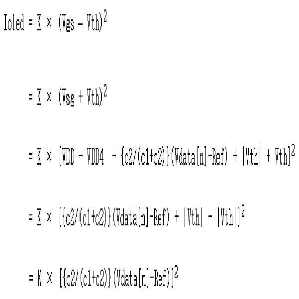
Therefore, the current Ioled flowing through the organic light emitting diode OLED can be determined by the current flowing in the driving transistor Tdr, and the current flowing through the driving transistor is the voltage Vgs between the gate electrode and the source electrode of the driving transistor, Is determined by the threshold voltage (Vth) of the transistor, and can be defined by the following Equation (1). On the other hand, the voltage at the first node N1, which is the gate electrode of the driving transistor Tdr, becomes equal to VDD4 + {c2 / (c1 + c2) by the voltage VC1 stored across the first capacitor C1 during the sampling period t3, c2)} (Vdata [n] - Ref) - | Vth |.
Here, " K " is a value determined by the structure and physical characteristics of the driving transistor Tdr as a proportional constant, and is a value obtained by dividing the mobility of the driving transistor Tdr and the channel width W of the driving transistor Tdr W / L " of the channel length L). In addition, when the transistors included in the organic light emitting diode display device are PMOS type transistors, the threshold voltage of the driving transistor has a negative value. On the other hand, the threshold voltage Vth of the driving transistor Tdr does not always have a constant value, but a deviation may occur depending on the operation state of the driving transistor Tdr.
In other words, according to
3, the first to third transistors are operated by control signals such as a scan signal Scan [n] and separate first and second emission control signals Em [n] and H [n] The second emission control signal H [n] is set to be the same as the emission control signal Em [n] of the first emission control signal Em [n] May be the next first emission control signal Em [n + 1], and the data voltage may also be applied every two horizontal periods.
Hereinafter, control signals according to another embodiment will be described with reference to FIG.
6 is a timing diagram according to another embodiment of the control signals supplied to the equivalent circuit shown in Fig.
As shown in FIG. 6, the data voltage is applied to the next data voltage every two horizontal periods (2H) unlike the data voltage shown in FIG. 5, and the reference voltage Ref is applied every two horizontal periods (2H) . It can also be seen that the second emission control signal H [n] is the (n + 1) th emission control signal Em [n + 1].
6, the organic light emitting diode display according to embodiments of the present invention includes an initialization period t1, a sensing period t2, a sampling period, The period t3 and the emission period t4 are divided into a
Therefore, the organic light emitting diode display according to embodiments of the present invention compensates for the deviation of the threshold voltage and the deviation of the high-potential power supply voltage due to the IR drop according to the operation state of the driving transistor, So that deterioration in image quality can be prevented.
Further, the organic light emitting diode display device according to the embodiments of the present invention can be adapted to a large area because the number of transistors and capacitors constituting the compensation circuit is small.
7 is a view for explaining a change in current according to a threshold voltage deviation of an organic light emitting diode display device according to embodiments of the present invention.
7, the magnitude of the current Ioled flowing through the organic light emitting diode OLED is proportional to the data voltage Vdata, but is equal to the deviation dVth of the threshold voltage Vth at the same data voltage Vdata It can be seen that it does not change much.
It will be understood by those skilled in the art that the present invention may be embodied in other specific forms without departing from the spirit or essential characteristics thereof.
It is therefore to be understood that the above-described embodiments are illustrative in all aspects and not restrictive. The scope of the present invention is defined by the appended claims rather than the detailed description and all changes or modifications derived from the meaning and scope of the claims and their equivalents are to be construed as being included within the scope of the present invention do.
T1 to T3: First to third transistors C1 and C2: First and second capacitors
Tdr: driving transistor OLED: organic light emitting diode
VDD: High-potential power supply voltage VSS: Low-potential power supply voltage
Claims (16)
A driving transistor having a gate electrode connected to the first node, a source electrode connected to the second node, and a drain electrode connected to the fourth node;
A first capacitor coupled between the first node and the second node, the first capacitor storing a threshold voltage of the driving transistor;
A second transistor for supplying a high potential power supply voltage applied to a third node to the second node according to a first emission control signal;
An organic light emitting diode whose emission is controlled according to a voltage difference between the first node and the second node; And
And a third transistor coupled between the fourth node and a fifth node, which is an anode electrode of the organic light emitting diode, according to a second emission control signal.
The first transistor is turned on by the scan signal applied through the scan line,
The second transistor is turned on by the first emission control signal applied through the first emission control line,
And the third transistor is turned on by the second emission control signal applied through the second emission control line.
Wherein the scan signal is an nth scan signal, the first emission control signal is an nth emission control signal, and the second emission control signal is an (n + 1) th emission control signal. Diode display.
And a second capacitor connected between the second node and the third node which is a source electrode of the second transistor.
When the first to third transistors are turned on,
Wherein the reference voltage is supplied to the first node, the high potential power supply voltage is supplied to the second node, and the fourth node and the fifth node are connected to each other.
When the first and third transistors are turned on and the second transistor is turned off,
Wherein the reference voltage is supplied to the first node, the fourth node and the fifth node are connected, and the second node voltage gradually decreases to a voltage smaller than the high potential power supply voltage. Display device.
Wherein the second node voltage is reduced to a sum of the reference voltage and an absolute value of a threshold voltage of the driving transistor.
When the first transistor is turned on and the second and third transistors are turned off,
And the data voltage is supplied to the first node.
When the first transistor is turned off and the second and third transistors are turned on,
Wherein the organic light emitting diode emits light according to the data voltage and the reference voltage.
Initializing a voltage of a first node, which is a gate electrode of the driving transistor, to a reference voltage according to a scan signal applied to the first transistor while the first through third transistors are turned on;
Wherein the first and third transistors are turned on and the second transistor is connected to a first node of which one end is connected to the first node and the other end is connected to a second node which is a source electrode of the driving transistor, Storing a threshold voltage of the driving transistor;
Supplying a data voltage to the first node while the first transistor is turned on and the second and third transistors are turned off; And
Wherein the organic light emitting diode emits light according to the data voltage and the reference voltage while the first transistor is turned off and the second and third transistors are turned on.
Wherein the initializing comprises:
And a fourth node that is a drain electrode of the driving transistor and a fifth node that is an anode electrode of the organic light emitting diode are connected to the second node.
Wherein the step of storing the threshold voltage comprises:
Wherein the reference voltage is supplied to the first node, and the second node voltage is reduced to a sum of the reference voltage and an absolute value of a threshold voltage of the driving transistor.
Wherein the second transistor has a source electrode connected to a third node to which a high potential power supply voltage is applied, a drain electrode connected to the second node, and a second capacitor connected between the second node and the third node, And driving the organic light emitting diode display device.
Wherein the step of supplying the data voltage comprises:
Wherein a connection between a fourth node which is a drain electrode of the driving transistor and a fifth node which is an anode electrode of the organic light emitting diode is cut off.
The first transistor is turned on by a scan signal applied through a scan line,
The second transistor is turned on by the first emission control signal applied through the first emission control line,
And the third transistor is turned on by a second emission control signal applied through a second emission control line.
Wherein the scan signal is an nth scan signal, the first emission control signal is an nth emission control signal, and the second emission control signal is an (n + 1) th emission control signal. A method of driving a diode display device.
Priority Applications (5)
| Application Number | Priority Date | Filing Date | Title |
|---|---|---|---|
| KR1020120152218A KR101411621B1 (en) | 2012-12-24 | 2012-12-24 | Organic light emitting diode display device and method for driving the same |
| EP13161924.9A EP2747064B1 (en) | 2012-12-24 | 2013-04-02 | Organic light emitting diode display device and method for driving the same |
| CN201310147032.XA CN103903556B (en) | 2012-12-24 | 2013-04-25 | Organic light-emitting diode (OLED) display apparatus and its driving method |
| US13/959,363 US10269294B2 (en) | 2012-12-24 | 2013-08-05 | Organic light emitting diode display device and method for driving the same |
| JP2013261291A JP5788480B2 (en) | 2012-12-24 | 2013-12-18 | Organic light emitting diode display device and driving method thereof |
Applications Claiming Priority (1)
| Application Number | Priority Date | Filing Date | Title |
|---|---|---|---|
| KR1020120152218A KR101411621B1 (en) | 2012-12-24 | 2012-12-24 | Organic light emitting diode display device and method for driving the same |
Publications (1)
| Publication Number | Publication Date |
|---|---|
| KR101411621B1 true KR101411621B1 (en) | 2014-07-02 |
Family
ID=48040052
Family Applications (1)
| Application Number | Title | Priority Date | Filing Date |
|---|---|---|---|
| KR1020120152218A KR101411621B1 (en) | 2012-12-24 | 2012-12-24 | Organic light emitting diode display device and method for driving the same |
Country Status (5)
| Country | Link |
|---|---|
| US (1) | US10269294B2 (en) |
| EP (1) | EP2747064B1 (en) |
| JP (1) | JP5788480B2 (en) |
| KR (1) | KR101411621B1 (en) |
| CN (1) | CN103903556B (en) |
Cited By (3)
| Publication number | Priority date | Publication date | Assignee | Title |
|---|---|---|---|---|
| KR20160049586A (en) * | 2014-10-27 | 2016-05-10 | 엘지디스플레이 주식회사 | Organic Light Emitting Display |
| KR20200061146A (en) * | 2018-11-23 | 2020-06-02 | 엘지디스플레이 주식회사 | Organic light emitting display panel and organic light emitting display apparatus using the same |
| US10720110B2 (en) | 2016-12-28 | 2020-07-21 | Lg Display Co., Ltd. | Electroluminescent display and method of driving the same |
Families Citing this family (19)
| Publication number | Priority date | Publication date | Assignee | Title |
|---|---|---|---|---|
| US20150145849A1 (en) * | 2013-11-26 | 2015-05-28 | Apple Inc. | Display With Threshold Voltage Compensation Circuitry |
| JP2016075836A (en) * | 2014-10-08 | 2016-05-12 | Nltテクノロジー株式会社 | Pixel circuit, method for driving the pixel circuit, and display device |
| KR20160055546A (en) * | 2014-11-10 | 2016-05-18 | 삼성디스플레이 주식회사 | Organic light emitting diode display |
| US9424782B2 (en) * | 2014-12-31 | 2016-08-23 | Lg Display Co., Ltd. | Organic light emitting display |
| CN104809989A (en) * | 2015-05-22 | 2015-07-29 | 京东方科技集团股份有限公司 | Pixel circuit, drive method thereof and related device |
| KR102411075B1 (en) * | 2015-08-24 | 2022-06-21 | 삼성디스플레이 주식회사 | Pixel and organic light emitting display device having the same |
| KR20170074618A (en) * | 2015-12-22 | 2017-06-30 | 엘지디스플레이 주식회사 | Sub-pixel of organic light emitting display device and organic light emitting display device including the same |
| CN106205494B (en) * | 2016-09-09 | 2019-05-31 | 深圳市华星光电技术有限公司 | AMOLED pixel-driving circuit and image element driving method |
| US10431142B2 (en) * | 2016-11-14 | 2019-10-01 | Int Tech Co., Ltd. | Pixel circuit and electroluminescent display comprising the pixel circuit |
| CN106991964A (en) | 2017-04-14 | 2017-07-28 | 京东方科技集团股份有限公司 | Image element circuit and its driving method, display device |
| KR102339644B1 (en) * | 2017-06-12 | 2021-12-15 | 엘지디스플레이 주식회사 | Electroluminescence display |
| CN107256695B (en) * | 2017-07-31 | 2019-11-19 | 上海天马有机发光显示技术有限公司 | Pixel circuit, its driving method, display panel and display device |
| CN108062932B (en) * | 2017-12-20 | 2020-05-26 | 北京航空航天大学 | Pixel circuit with organic thin film transistor structure |
| CN110070825B (en) | 2018-06-14 | 2020-10-09 | 友达光电股份有限公司 | Pixel circuit |
| CN110164376B (en) * | 2018-08-22 | 2020-11-03 | 合肥视涯技术有限公司 | Pixel circuit of organic light-emitting display device and driving method thereof |
| CN109102775B (en) | 2018-08-31 | 2021-02-02 | 武汉天马微电子有限公司 | Organic light emitting diode compensation circuit, display panel and display device |
| KR102631739B1 (en) * | 2018-11-29 | 2024-01-30 | 엘지디스플레이 주식회사 | Subpixel driving circuit and electroluminescent display device having the same |
| CN109584787A (en) * | 2019-01-21 | 2019-04-05 | 惠科股份有限公司 | A kind of driving circuit of display panel, driving method and display device |
| TWI780844B (en) * | 2021-07-29 | 2022-10-11 | 友達光電股份有限公司 | Driving circuit |
Citations (4)
| Publication number | Priority date | Publication date | Assignee | Title |
|---|---|---|---|---|
| KR20090016333A (en) * | 2007-08-10 | 2009-02-13 | 엘지디스플레이 주식회사 | Elector-luminescent pixel and display panel and device having the same |
| KR20090057484A (en) * | 2007-12-03 | 2009-06-08 | 엘지디스플레이 주식회사 | Organic light emitting diode display and driving method thereof |
| KR20110072283A (en) * | 2009-12-22 | 2011-06-29 | 엘지디스플레이 주식회사 | Organic light emitting display device |
| KR20130019620A (en) * | 2011-08-17 | 2013-02-27 | 엘지디스플레이 주식회사 | Organic light emitting diode display device |
Family Cites Families (24)
| Publication number | Priority date | Publication date | Assignee | Title |
|---|---|---|---|---|
| US20040257352A1 (en) * | 2003-06-18 | 2004-12-23 | Nuelight Corporation | Method and apparatus for controlling |
| KR100560780B1 (en) * | 2003-07-07 | 2006-03-13 | 삼성에스디아이 주식회사 | Pixel circuit in OLED and Method for fabricating the same |
| TW200620207A (en) * | 2004-07-05 | 2006-06-16 | Sony Corp | Pixel circuit, display device, driving method of pixel circuit, and driving method of display device |
| CA2536398A1 (en) | 2006-02-10 | 2007-08-10 | G. Reza Chaji | A method for extracting the aging factor of flat panels and calibration of programming/biasing |
| JP4984715B2 (en) * | 2006-07-27 | 2012-07-25 | ソニー株式会社 | Display device driving method and display element driving method |
| JP4203773B2 (en) * | 2006-08-01 | 2009-01-07 | ソニー株式会社 | Display device |
| JP4300490B2 (en) * | 2007-02-21 | 2009-07-22 | ソニー株式会社 | Display device, driving method thereof, and electronic apparatus |
| KR100882907B1 (en) | 2007-06-21 | 2009-02-10 | 삼성모바일디스플레이주식회사 | Organic Light Emitting Diode Display Device |
| KR20090101578A (en) * | 2008-03-24 | 2009-09-29 | 삼성모바일디스플레이주식회사 | Pixel and organic light emitting display device using the same |
| JP2009258397A (en) | 2008-04-17 | 2009-11-05 | Toshiba Mobile Display Co Ltd | Method of driving el display device |
| KR101341011B1 (en) * | 2008-05-17 | 2013-12-13 | 엘지디스플레이 주식회사 | Light emitting display |
| US8405582B2 (en) * | 2008-06-11 | 2013-03-26 | Samsung Display Co., Ltd. | Organic light emitting display and driving method thereof |
| CN101960509B (en) * | 2008-07-04 | 2015-04-15 | 松下电器产业株式会社 | Display device and method for controlling the same |
| JP5308796B2 (en) * | 2008-11-28 | 2013-10-09 | グローバル・オーエルイーディー・テクノロジー・リミテッド・ライアビリティ・カンパニー | Display device and pixel circuit |
| JP5287210B2 (en) | 2008-12-17 | 2013-09-11 | ソニー株式会社 | Display device and electronic device |
| JP5302915B2 (en) * | 2009-03-18 | 2013-10-02 | パナソニック株式会社 | Organic EL display device and control method |
| KR101056297B1 (en) * | 2009-11-03 | 2011-08-11 | 삼성모바일디스플레이주식회사 | Pixel and organic light emitting display device having same |
| KR101752778B1 (en) * | 2010-06-25 | 2017-07-03 | 엘지디스플레이 주식회사 | Organic Electroluminescent display device and method of driving the same |
| JP5719571B2 (en) | 2010-11-15 | 2015-05-20 | 株式会社ジャパンディスプレイ | Display device and driving method of display device |
| KR102040843B1 (en) * | 2011-01-04 | 2019-11-06 | 삼성디스플레이 주식회사 | Organic light emitting display and driving method thereof |
| TWI425472B (en) | 2011-11-18 | 2014-02-01 | Au Optronics Corp | Pixel circuit and driving method thereof |
| TWI451384B (en) * | 2011-12-30 | 2014-09-01 | Au Optronics Corp | Pixel structure, driving method thereof and self-emitting display using the same |
| JP5494684B2 (en) * | 2012-01-20 | 2014-05-21 | セイコーエプソン株式会社 | Driving method of electronic circuit |
| KR101411619B1 (en) * | 2012-09-27 | 2014-06-25 | 엘지디스플레이 주식회사 | Pixel circuit and method for driving thereof, and organic light emitting display device using the same |
-
2012
- 2012-12-24 KR KR1020120152218A patent/KR101411621B1/en active IP Right Grant
-
2013
- 2013-04-02 EP EP13161924.9A patent/EP2747064B1/en active Active
- 2013-04-25 CN CN201310147032.XA patent/CN103903556B/en active Active
- 2013-08-05 US US13/959,363 patent/US10269294B2/en active Active
- 2013-12-18 JP JP2013261291A patent/JP5788480B2/en active Active
Patent Citations (4)
| Publication number | Priority date | Publication date | Assignee | Title |
|---|---|---|---|---|
| KR20090016333A (en) * | 2007-08-10 | 2009-02-13 | 엘지디스플레이 주식회사 | Elector-luminescent pixel and display panel and device having the same |
| KR20090057484A (en) * | 2007-12-03 | 2009-06-08 | 엘지디스플레이 주식회사 | Organic light emitting diode display and driving method thereof |
| KR20110072283A (en) * | 2009-12-22 | 2011-06-29 | 엘지디스플레이 주식회사 | Organic light emitting display device |
| KR20130019620A (en) * | 2011-08-17 | 2013-02-27 | 엘지디스플레이 주식회사 | Organic light emitting diode display device |
Cited By (5)
| Publication number | Priority date | Publication date | Assignee | Title |
|---|---|---|---|---|
| KR20160049586A (en) * | 2014-10-27 | 2016-05-10 | 엘지디스플레이 주식회사 | Organic Light Emitting Display |
| KR102328983B1 (en) * | 2014-10-27 | 2021-11-23 | 엘지디스플레이 주식회사 | Organic Light Emitting Display |
| US10720110B2 (en) | 2016-12-28 | 2020-07-21 | Lg Display Co., Ltd. | Electroluminescent display and method of driving the same |
| KR20200061146A (en) * | 2018-11-23 | 2020-06-02 | 엘지디스플레이 주식회사 | Organic light emitting display panel and organic light emitting display apparatus using the same |
| KR102646487B1 (en) | 2018-11-23 | 2024-03-12 | 엘지디스플레이 주식회사 | Organic light emitting display panel and organic light emitting display apparatus using the same |
Also Published As
| Publication number | Publication date |
|---|---|
| CN103903556B (en) | 2017-09-08 |
| EP2747064B1 (en) | 2017-07-12 |
| US20140176523A1 (en) | 2014-06-26 |
| JP2014123127A (en) | 2014-07-03 |
| JP5788480B2 (en) | 2015-09-30 |
| EP2747064A1 (en) | 2014-06-25 |
| US10269294B2 (en) | 2019-04-23 |
| CN103903556A (en) | 2014-07-02 |
Similar Documents
| Publication | Publication Date | Title |
|---|---|---|
| KR101411621B1 (en) | Organic light emitting diode display device and method for driving the same | |
| KR101486538B1 (en) | Organic light emitting diode display device and method for driving the same | |
| KR102006702B1 (en) | Organic light emitting diode display device and method for driving the same | |
| KR101360768B1 (en) | Organic light emitting diode display device and method for driving the same | |
| KR101341797B1 (en) | Organic light emitting diode display device and method for driving the same | |
| KR102187835B1 (en) | Organic light emitting diode display device and method for driving the same | |
| KR102141238B1 (en) | Pixel and Organic Light Emitting Display Device | |
| US9111488B2 (en) | Organic light emitting diode display device and method of driving the same | |
| JP6082784B2 (en) | Driving method of organic light emitting diode display device | |
| KR101360767B1 (en) | Organic light emitting diode display device and method for driving the same | |
| KR20150064544A (en) | Organic light emitting diode display device and method for driving the same | |
| KR20140062545A (en) | Pixel, display device comprising the same and driving method thereof | |
| KR20150064545A (en) | Organic light emitting diode display device and method for driving the same | |
| KR101980770B1 (en) | Organic light emitting diode display device | |
| KR20180071896A (en) | Light emitting display device and driving method for the same | |
| KR101666589B1 (en) | Organic light emitting diode display device and method for driving the same | |
| KR102023438B1 (en) | Organic light emitting diode display device and method for driving the same | |
| KR20160015509A (en) | Organic light emitting display device |
Legal Events
| Date | Code | Title | Description |
|---|---|---|---|
| A201 | Request for examination | ||
| E701 | Decision to grant or registration of patent right | ||
| GRNT | Written decision to grant | ||
| FPAY | Annual fee payment |
Payment date: 20180515 Year of fee payment: 5 |
|
| FPAY | Annual fee payment |
Payment date: 20190515 Year of fee payment: 6 |