WO2023157330A1 - 半導体装置およびその製造方法 - Google Patents
半導体装置およびその製造方法 Download PDFInfo
- Publication number
- WO2023157330A1 WO2023157330A1 PCT/JP2022/024121 JP2022024121W WO2023157330A1 WO 2023157330 A1 WO2023157330 A1 WO 2023157330A1 JP 2022024121 W JP2022024121 W JP 2022024121W WO 2023157330 A1 WO2023157330 A1 WO 2023157330A1
- Authority
- WO
- WIPO (PCT)
- Prior art keywords
- region
- peak
- atomic density
- dopant
- semiconductor substrate
- Prior art date
- Legal status (The legal status is an assumption and is not a legal conclusion. Google has not performed a legal analysis and makes no representation as to the accuracy of the status listed.)
- Ceased
Links
Images


Classifications
-
- H—ELECTRICITY
- H10—SEMICONDUCTOR DEVICES; ELECTRIC SOLID-STATE DEVICES NOT OTHERWISE PROVIDED FOR
- H10D—INORGANIC ELECTRIC SEMICONDUCTOR DEVICES
- H10D12/00—Bipolar devices controlled by the field effect, e.g. insulated-gate bipolar transistors [IGBT]
-
- H—ELECTRICITY
- H10—SEMICONDUCTOR DEVICES; ELECTRIC SOLID-STATE DEVICES NOT OTHERWISE PROVIDED FOR
- H10D—INORGANIC ELECTRIC SEMICONDUCTOR DEVICES
- H10D12/00—Bipolar devices controlled by the field effect, e.g. insulated-gate bipolar transistors [IGBT]
- H10D12/01—Manufacture or treatment
- H10D12/031—Manufacture or treatment of IGBTs
- H10D12/032—Manufacture or treatment of IGBTs of vertical IGBTs
- H10D12/038—Manufacture or treatment of IGBTs of vertical IGBTs having a recessed gate, e.g. trench-gate IGBTs
-
- H—ELECTRICITY
- H10—SEMICONDUCTOR DEVICES; ELECTRIC SOLID-STATE DEVICES NOT OTHERWISE PROVIDED FOR
- H10D—INORGANIC ELECTRIC SEMICONDUCTOR DEVICES
- H10D12/00—Bipolar devices controlled by the field effect, e.g. insulated-gate bipolar transistors [IGBT]
- H10D12/411—Insulated-gate bipolar transistors [IGBT]
- H10D12/441—Vertical IGBTs
- H10D12/461—Vertical IGBTs having non-planar surfaces, e.g. having trenches, recesses or pillars in the surfaces of the emitter, base or collector regions
- H10D12/481—Vertical IGBTs having non-planar surfaces, e.g. having trenches, recesses or pillars in the surfaces of the emitter, base or collector regions having gate structures on slanted surfaces, on vertical surfaces, or in grooves, e.g. trench gate IGBTs
-
- H—ELECTRICITY
- H10—SEMICONDUCTOR DEVICES; ELECTRIC SOLID-STATE DEVICES NOT OTHERWISE PROVIDED FOR
- H10D—INORGANIC ELECTRIC SEMICONDUCTOR DEVICES
- H10D62/00—Semiconductor bodies, or regions thereof, of devices having potential barriers
- H10D62/10—Shapes, relative sizes or dispositions of the regions of the semiconductor bodies; Shapes of the semiconductor bodies
- H10D62/102—Constructional design considerations for preventing surface leakage or controlling electric field concentration
- H10D62/112—Constructional design considerations for preventing surface leakage or controlling electric field concentration for preventing surface leakage due to surface inversion layers, e.g. by using channel stoppers
-
- H—ELECTRICITY
- H10—SEMICONDUCTOR DEVICES; ELECTRIC SOLID-STATE DEVICES NOT OTHERWISE PROVIDED FOR
- H10D—INORGANIC ELECTRIC SEMICONDUCTOR DEVICES
- H10D62/00—Semiconductor bodies, or regions thereof, of devices having potential barriers
- H10D62/10—Shapes, relative sizes or dispositions of the regions of the semiconductor bodies; Shapes of the semiconductor bodies
- H10D62/13—Semiconductor regions connected to electrodes carrying current to be rectified, amplified or switched, e.g. source or drain regions
- H10D62/141—Anode or cathode regions of thyristors; Collector or emitter regions of gated bipolar-mode devices, e.g. of IGBTs
- H10D62/142—Anode regions of thyristors or collector regions of gated bipolar-mode devices
-
- H—ELECTRICITY
- H10—SEMICONDUCTOR DEVICES; ELECTRIC SOLID-STATE DEVICES NOT OTHERWISE PROVIDED FOR
- H10D—INORGANIC ELECTRIC SEMICONDUCTOR DEVICES
- H10D62/00—Semiconductor bodies, or regions thereof, of devices having potential barriers
- H10D62/60—Impurity distributions or concentrations
-
- H—ELECTRICITY
- H10—SEMICONDUCTOR DEVICES; ELECTRIC SOLID-STATE DEVICES NOT OTHERWISE PROVIDED FOR
- H10D—INORGANIC ELECTRIC SEMICONDUCTOR DEVICES
- H10D62/00—Semiconductor bodies, or regions thereof, of devices having potential barriers
- H10D62/80—Semiconductor bodies, or regions thereof, of devices having potential barriers characterised by the materials
- H10D62/81—Semiconductor bodies, or regions thereof, of devices having potential barriers characterised by the materials of structures exhibiting quantum-confinement effects, e.g. single quantum wells; of structures having periodic or quasi-periodic potential variation
-
- H—ELECTRICITY
- H10—SEMICONDUCTOR DEVICES; ELECTRIC SOLID-STATE DEVICES NOT OTHERWISE PROVIDED FOR
- H10D—INORGANIC ELECTRIC SEMICONDUCTOR DEVICES
- H10D8/00—Diodes
- H10D8/422—PN diodes having the PN junctions in mesas
-
- H—ELECTRICITY
- H10—SEMICONDUCTOR DEVICES; ELECTRIC SOLID-STATE DEVICES NOT OTHERWISE PROVIDED FOR
- H10D—INORGANIC ELECTRIC SEMICONDUCTOR DEVICES
- H10D84/00—Integrated devices formed in or on semiconductor substrates that comprise only semiconducting layers, e.g. on Si wafers or on GaAs-on-Si wafers
- H10D84/60—Integrated devices formed in or on semiconductor substrates that comprise only semiconducting layers, e.g. on Si wafers or on GaAs-on-Si wafers characterised by the integration of at least one component covered by groups H10D10/00 or H10D18/00, e.g. integration of BJTs
- H10D84/611—Combinations of BJTs and one or more of diodes, resistors or capacitors
- H10D84/613—Combinations of vertical BJTs and one or more of diodes, resistors or capacitors
- H10D84/617—Combinations of vertical BJTs and only diodes
-
- H—ELECTRICITY
- H10—SEMICONDUCTOR DEVICES; ELECTRIC SOLID-STATE DEVICES NOT OTHERWISE PROVIDED FOR
- H10P—GENERIC PROCESSES OR APPARATUS FOR THE MANUFACTURE OR TREATMENT OF DEVICES COVERED BY CLASS H10
- H10P30/00—Ion implantation into wafers, substrates or parts of devices
- H10P30/20—Ion implantation into wafers, substrates or parts of devices into semiconductor materials, e.g. for doping
- H10P30/202—Ion implantation into wafers, substrates or parts of devices into semiconductor materials, e.g. for doping characterised by the semiconductor materials
- H10P30/204—Ion implantation into wafers, substrates or parts of devices into semiconductor materials, e.g. for doping characterised by the semiconductor materials into Group IV semiconductors
-
- H—ELECTRICITY
- H10—SEMICONDUCTOR DEVICES; ELECTRIC SOLID-STATE DEVICES NOT OTHERWISE PROVIDED FOR
- H10P—GENERIC PROCESSES OR APPARATUS FOR THE MANUFACTURE OR TREATMENT OF DEVICES COVERED BY CLASS H10
- H10P30/00—Ion implantation into wafers, substrates or parts of devices
- H10P30/20—Ion implantation into wafers, substrates or parts of devices into semiconductor materials, e.g. for doping
- H10P30/21—Ion implantation into wafers, substrates or parts of devices into semiconductor materials, e.g. for doping of electrically active species
-
- H—ELECTRICITY
- H10—SEMICONDUCTOR DEVICES; ELECTRIC SOLID-STATE DEVICES NOT OTHERWISE PROVIDED FOR
- H10P—GENERIC PROCESSES OR APPARATUS FOR THE MANUFACTURE OR TREATMENT OF DEVICES COVERED BY CLASS H10
- H10P30/00—Ion implantation into wafers, substrates or parts of devices
- H10P30/20—Ion implantation into wafers, substrates or parts of devices into semiconductor materials, e.g. for doping
- H10P30/28—Ion implantation into wafers, substrates or parts of devices into semiconductor materials, e.g. for doping characterised by an annealing step, e.g. for activation of dopants
-
- H—ELECTRICITY
- H10—SEMICONDUCTOR DEVICES; ELECTRIC SOLID-STATE DEVICES NOT OTHERWISE PROVIDED FOR
- H10P—GENERIC PROCESSES OR APPARATUS FOR THE MANUFACTURE OR TREATMENT OF DEVICES COVERED BY CLASS H10
- H10P34/00—Irradiation with electromagnetic or particle radiation of wafers, substrates or parts of devices
- H10P34/40—Irradiation with electromagnetic or particle radiation of wafers, substrates or parts of devices with high-energy radiation
- H10P34/42—Irradiation with electromagnetic or particle radiation of wafers, substrates or parts of devices with high-energy radiation with electromagnetic radiation, e.g. laser annealing
-
- H—ELECTRICITY
- H10—SEMICONDUCTOR DEVICES; ELECTRIC SOLID-STATE DEVICES NOT OTHERWISE PROVIDED FOR
- H10D—INORGANIC ELECTRIC SEMICONDUCTOR DEVICES
- H10D64/00—Electrodes of devices having potential barriers
- H10D64/111—Field plates
- H10D64/117—Recessed field plates, e.g. trench field plates or buried field plates
-
- H—ELECTRICITY
- H10—SEMICONDUCTOR DEVICES; ELECTRIC SOLID-STATE DEVICES NOT OTHERWISE PROVIDED FOR
- H10D—INORGANIC ELECTRIC SEMICONDUCTOR DEVICES
- H10D84/00—Integrated devices formed in or on semiconductor substrates that comprise only semiconducting layers, e.g. on Si wafers or on GaAs-on-Si wafers
- H10D84/80—Integrated devices formed in or on semiconductor substrates that comprise only semiconducting layers, e.g. on Si wafers or on GaAs-on-Si wafers characterised by the integration of at least one component covered by groups H10D12/00 or H10D30/00, e.g. integration of IGFETs
- H10D84/811—Combinations of field-effect devices and one or more diodes, capacitors or resistors
Definitions
- the present invention relates to a semiconductor device and its manufacturing method.
- Patent Literature 1 describes that "the n-type impurity concentration gradually increases from the lower surface 12b of the semiconductor substrate 12 toward the deeper side, reaching a maximum value N1".
- Non-Patent Document 1 describes forming a BOX profile on the back surface.
- Patent Document 1 JP-A-2015-153788
- Patent Document 2 JP-A-2016-004956
- Non-Patent Document 1 Seino et al., "Development of Top Flat Beam Hybrid Laser Annealer for Deep Activation of Power Semiconductor IGBT", Japan Steel Works Technical Report No.69, p.76-81 (2018.11)
- a drift region of a first conductivity type is provided in a semiconductor substrate having a front surface and a back surface;
- a semiconductor device comprising: a first conductivity type or second conductivity type back side region having a higher atomic density than the drift region.
- the atomic density distribution of the back surface side region includes a gentle gradient region where the dopant atomic density increases from the back surface side toward the front surface side of the semiconductor substrate, and the gentle gradient region.
- a steep region provided closer to the front surface side than the region, where the atomic density gradient of the dopant increases with an atomic density gradient greater than that of the gentle slope region; a peak region having a peak in the atomic density distribution of the dopant; and a peak region provided between the peak region and the drift region, wherein atoms of the dopant are directed toward the drift region in the depth direction of the semiconductor substrate. and a depleted region of decreasing density.
- the depth of the peak of the atomic density distribution from the back surface of the semiconductor substrate may be 0.8 ⁇ m or less.
- the average atomic density in the gentle gradient region may be 20% or more and 95% or less of the peak atomic density of the peak of the atomic density distribution.
- any of the above semiconductor devices may include an edge termination structure provided on the front surface of the semiconductor substrate.
- the upper end of the gentle slope region may be positioned midway between the back surface and the depth position of the peak of the peak region in the depth direction of the semiconductor substrate.
- the lower end of the gentle slope region may be the back surface of the semiconductor substrate.
- the lower end of the peak region may be located on the back surface side of the semiconductor substrate relative to the peak, where the atomic density of the dopant at the peak is 95%.
- the upper end of the peak region may be a position on the front surface side of the semiconductor substrate with respect to the peak, where the density is 95% of the atomic density of the dopant at the peak.
- the upper end of the reduced region is located closer to the front surface of the semiconductor substrate than the peak and has a density of 10% of the atomic density of the dopant at the peak. you can
- the upper end of the gentle slope region may be in contact with the lower end of the steep slope region.
- the upper end of the steep region may meet the lower end of the peak region.
- the top edge of the peak region may contact the bottom edge of the depletion region.
- Any one of the above semiconductor devices may include a transistor section.
- the back side region may include a second conductivity type collector region.
- the dopant in the collector region may be boron.
- the gentle gradient region has an atomic density gradient of the dopant of 1.0E21 [atoms/cm 4 ] or more and 5.0E23 [atoms/cm 4 ] or less. good.
- the atomic density gradient of the dopant in the steep region is 1.0E22 [atoms/cm 4 ] or more and 1.0E24 [atoms/cm 4 ] or less. good.
- an atomic density gradient of the dopant in the reduced region may be 1.0E23 [atoms/cm 4 ] or more and 1.0E25 [atoms/cm 4 ] or less. .
- an atomic density of the dopant at a peak of the peak region may be 1.0E+16 [cm ⁇ 3 ] or more and 1.0E+20 [cm ⁇ 3 ] or less.
- the dopant atomic density at the lower end of the gentle gradient region may be 10% or more and 80% or less of the dopant atomic density at the peak of the peak region.
- the ratio of the atomic density gradient of the gentle gradient region to the dopant atomic density gradient of the steep gradient region may be 0.01 or more and 0.8 or less.
- the ratio of the dopant atomic density gradient in the steep region to the dopant atomic density gradient in the reduced region is 0.001 or more and 0.5 or less. you can
- Any one of the above semiconductor devices may include a diode section.
- the back side region may include a first conductivity type cathode region.
- the dopant in the cathode region may be phosphorus.
- the dopant atomic density gradient in the gentle gradient region is 1.0E22 [atoms/cm 4 ] or more and 2.0E24 [atoms/cm 4 ] or less. good.
- the dopant atomic density gradient in the steep region is 1.0E23 [atoms/cm 4 ] or more and 1.0E25 [atoms/cm 4 ] or less. good.
- the dopant atomic density gradient in the reduced region may be 2.0E24 [atoms/cm 4 ] or more and 2.0E26 [atoms/cm 4 ] or less. .
- the dopant atom density at the peak of the peak region may be 1.0E [19 cm -3 ] or more and 1.0E [21 cm -3 ] or less.
- the dopant atomic density at the lower end of the gentle gradient region may be 30% or more and 90% or less of the dopant atomic density at the peak of the peak region.
- the ratio of the dopant atomic density gradient in the gentle gradient region to the dopant atomic density gradient in the steep gradient region is 0.01 or more and 0.5 or less. It's okay.
- the ratio of the dopant atomic density gradient in the steep region to the dopant atomic density gradient in the reduced region is 0.001 or more and 0.3 or less. you can
- the doping concentration of the dopant at the peak of the peak region may be 10% or more and 80% or less of the atomic density of the dopant at the peak of the peak region.
- the doping concentration distribution of the back side region may include a doping peak region having a peak in the doping concentration distribution in the peak region.
- manufacturing a semiconductor device comprising the steps of: implanting dopant ions into the back surface of a semiconductor substrate having a front surface and a back surface; and irradiating the back surface of the semiconductor substrate with a laser.
- the melting depth of the semiconductor substrate melted by the laser irradiation may include a peak depth position of the atomic density distribution of the dopant after the step of ion-implanting the dopant.
- the depth position of the peak of the atomic density distribution of the dopant is adjusted to the atomic density distribution of the dopant in the step of implanting the ions.
- a redistribution step of redistributing to the front surface side of the semiconductor substrate from the peak position may be included.
- the redistribution step may include precipitating the dopant on the front surface side by melting the irradiated region.
- the step of forming a drift region of a first conductivity type; and forming a backside region of a conductivity type or a second conductivity type includes implanting ions of a dopant into the back surface of the semiconductor substrate; forming a gentle gradient region in which the atomic density of the dopant increases; and increasing the atomic density of the dopant with a greater atomic density gradient than the gentle gradient region toward the front surface side of the gentle gradient region.
- a steep region forming a peak region having a peak in the atomic density distribution closer to the front surface than the steep region; between the peak region and the drift region; and forming a depletion region in a depth direction of the semiconductor substrate toward the drift region where the atomic density of the dopant is reduced.
- the step of forming the back side region may include the step of laser annealing the semiconductor substrate from the back side of the semiconductor substrate.
- the melting depth of the semiconductor substrate melted by laser irradiation is the peak position of the atomic density of the dopant after ion implantation or the peak. It should be deeper than the position.
- the step of laser annealing is performed so that the peak position of the atomic density distribution of the dopant after ion implantation is reduced by melting of the irradiated region of the semiconductor substrate by the laser annealing.
- a step of redistributing a peak of the atomic density distribution of the dopant to a position on the front side of the semiconductor substrate may be included.
- the step of redistributing the peaks of the atomic density distribution may include the step of precipitating the dopant on the front surface side by melting the irradiated region.
- the step of forming the back-side region may not include thermal annealing for forming the back-side region.
- FIG. 1A shows an example of aa' cross section in FIG. 1A.
- 6 is an example of a graph showing the atomic density distribution of the back side region 60.
- FIG. 6 is an example of a graph showing the atomic density gradient of the gentle gradient region 61.
- FIG. 6 is an example of a graph showing an atomic density gradient in a steep region 62;
- 6 is an example of a graph showing an atomic density gradient in a depletion region 64;
- FIG. 10 is an example of a top view showing a modification of the semiconductor device 100;
- 3B is an enlarged view of area A in FIG. 3A;
- FIG. A bb' cross section of a modified example of the semiconductor device 100 is shown.
- FIG. 6 is an example of a graph showing the atomic density distribution of the back side region 60.
- FIG. 6 is an example of a graph showing the atomic density gradient of the gentle gradient region 61.
- FIG. 6 is an example of a graph showing an atomic density gradient in a steep region 62;
- 6 is an example of a graph showing an atomic density gradient in a depletion region 64;
- 4 is a flow chart showing an example of a manufacturing process of the semiconductor device 100;
- the atomic density distribution before and after laser annealing of the back side region 60 is shown.
- 3 shows the measurement results of the atomic density on the back surface 23 side of the semiconductor substrate 10.
- FIG. 3 shows the measurement results of the doping concentration on the back surface 23 side of the semiconductor substrate 10.
- one side in the direction parallel to the depth direction of the semiconductor substrate is called “upper”, and the other side is called “lower”.
- One of the two main surfaces of a substrate, layer or other member is called the upper surface and the other surface is called the lower surface.
- the directions of “up” and “down” are not limited to the direction of gravity or the direction when the semiconductor device is mounted.
- the Cartesian coordinate axes only specify the relative positions of the components and do not limit any particular orientation.
- the Z axis does not limit the height direction with respect to the ground.
- the +Z-axis direction and the ⁇ Z-axis direction are directions opposite to each other.
- the Z-axis direction is described without indicating positive or negative, it means a direction parallel to the +Z-axis and -Z-axis.
- orthogonal axes parallel to the upper and lower surfaces of the semiconductor substrate are defined as the X-axis and the Y-axis.
- the axis perpendicular to the upper and lower surfaces of the semiconductor substrate is defined as the Z-axis.
- the Z-axis direction may be referred to as the depth direction.
- a direction parallel to the upper and lower surfaces of the semiconductor substrate, including the X-axis and Y-axis may be referred to as a horizontal direction.
- the conductivity type of the doping region doped with impurities is described as P-type or N-type.
- impurities may specifically refer to either N-type donors or P-type acceptors, and may also be referred to as dopants.
- doping means introducing donors or acceptors into a semiconductor substrate to make it a semiconductor exhibiting N-type conductivity or a semiconductor exhibiting P-type conductivity.
- doping concentration means the concentration of donors or the concentration of acceptors at thermal equilibrium.
- the net doping concentration means the net concentration including charge polarity, where the donor concentration is the positive ion concentration and the acceptor concentration is the negative ion concentration.
- the donor concentration is N D and the acceptor concentration is N A , then the net net doping concentration at any location is N D ⁇ N A.
- net doping concentration may be simply referred to as doping concentration.
- a donor has the function of supplying electrons to a semiconductor.
- the acceptor has the function of receiving electrons from the semiconductor.
- Donors and acceptors are not limited to impurities per se.
- a VOH defect which is a combination of vacancies (V), oxygen (O), and hydrogen (H) present in a semiconductor, functions as a donor that supplies electrons.
- VOH defects are sometimes referred to herein as hydrogen donors.
- references herein to P-type or N-type refer to higher doping concentrations than P-type or N-type; references to P-type or N-type refer to higher doping than P-type or N-type. It means that the concentration is low.
- the term P++ type or N++ type in this specification means that the doping concentration is higher than that of the P+ type or N+ type.
- chemical concentration refers to the atomic density of impurities measured regardless of the state of electrical activation. Chemical concentrations can be measured, for example, by secondary ion mass spectroscopy (SIMS).
- the net doping concentrations mentioned above can be measured by the voltage-capacitance method (CV method).
- the carrier concentration measured by the spreading resistance measurement method (SR method) may be used as the net doping concentration.
- carrier is meant an electron or hole charge carrier.
- the carrier concentration measured by the CV method or SR method may be a value in thermal equilibrium.
- the carrier concentration in the region may be used as the donor concentration.
- the carrier concentration in that region may be used as the acceptor concentration.
- the doping concentration of the N-type regions is sometimes referred to herein as the donor concentration, and the doping concentration of the P-type regions is sometimes referred to as the acceptor concentration.
- the peak value may be the concentration of donors, acceptors, or net doping in the region.
- the average value of the concentration of donors, acceptors or net doping in the region may be used as the concentration of donors, acceptors or net doping.
- the carrier concentration measured by the SR method may be lower than the donor or acceptor concentration.
- the carrier mobility of the semiconductor substrate In the range through which the current flows when measuring the spreading resistance, the carrier mobility of the semiconductor substrate may be lower than the value in the crystalline state.
- a decrease in carrier mobility is caused by scattering of carriers due to disorder of the crystal structure due to lattice defects or the like.
- the reason for the decrease in carrier concentration is as follows.
- the SR method the spreading resistance is measured, and the measured value of the spreading resistance is converted into the carrier concentration. At this time, the mobility of the crystalline state is used as the carrier mobility.
- the carrier concentration is calculated from the carrier mobility in the crystalline state, although the carrier mobility is lowered. Therefore, the value is lower than the actual carrier concentration, that is, the donor or acceptor concentration.
- the donor or acceptor concentration calculated from the carrier concentration measured by the CV method or the SR method may be lower than the chemical concentration of the element representing the donor or acceptor.
- the donor concentration of phosphorus or arsenic as a donor or the acceptor concentration of boron (boron) as an acceptor in a silicon semiconductor is about 99% of these chemical concentrations.
- the donor concentration of hydrogen serving as a donor in a silicon semiconductor is about 0.1% to 10% of the chemical concentration of hydrogen.
- the SI unit system is adopted. In this specification, the units of distance and length are sometimes expressed in cm (centimeter). In this case, various calculations may be made by converting to m (meters). For numeric representations of powers of 10, for example, a representation of 1E+16 indicates 1 ⁇ 10 16 and a representation of 1E ⁇ 16 indicates 1 ⁇ 10 ⁇ 16 .
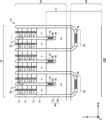
- FIG. 1A shows an example of a top view of the semiconductor device 100.
- FIG. A semiconductor device 100 of this example is a semiconductor chip including a transistor section 70 .
- the transistor portion 70 is a region obtained by projecting the collector region 22 provided on the back surface side of the semiconductor substrate 10 onto the upper surface of the semiconductor substrate 10 .
- the collector region 22 will be described later.
- the transistor section 70 includes transistors such as IGBTs.
- the transistor section 70 is an IGBT.
- the transistor section 70 may be another transistor such as a MOSFET.
- an edge termination structure portion may be provided in the region on the negative side in the Y-axis direction of the semiconductor device 100 of this example.
- the edge termination structure relieves electric field concentration on the top side of the semiconductor substrate 10 .
- Edge termination structures include, for example, guard rings, field plates, RESURF, and combinations thereof. In this example, for the sake of convenience, the edge on the negative side in the Y-axis direction will be described, but the other edges of the semiconductor device 100 are the same.
- the semiconductor substrate 10 is a substrate made of a semiconductor material.
- the semiconductor substrate 10 may be a silicon substrate, a silicon carbide substrate, a nitride semiconductor substrate such as gallium nitride, or the like.
- the semiconductor substrate 10 of this example is a silicon substrate.
- the term "top view” simply means that the semiconductor substrate 10 is viewed from the top side.
- the semiconductor device 100 of this example includes a gate trench portion 40, a dummy trench portion 30, an emitter region 12, a base region 14, a contact region 15, and a well region 17 on the front surface 21 of the semiconductor substrate 10. Prepare. The front surface 21 will be described later.
- the semiconductor device 100 of this example also includes an emitter electrode 52 and a gate metal layer 50 provided above the front surface 21 of the semiconductor substrate 10 .
- the emitter electrode 52 is provided above the gate trench portion 40 , the dummy trench portion 30 , the emitter region 12 , the base region 14 , the contact region 15 and the well region 17 . Also, the gate metal layer 50 is provided above the gate trench portion 40 and the well region 17 .
- the emitter electrode 52 and the gate metal layer 50 are made of a material containing metal. At least a partial region of the emitter electrode 52 may be made of a metal such as aluminum (Al) or a metal alloy such as an aluminum-silicon alloy (AlSi) or an aluminum-silicon-copper alloy (AlSiCu). At least a partial region of the gate metal layer 50 may be made of a metal such as aluminum (Al) or a metal alloy such as an aluminum-silicon alloy (AlSi) or an aluminum-silicon-copper alloy (AlSiCu).
- the emitter electrode 52 and the gate metal layer 50 may have a barrier metal made of titanium, a titanium compound or the like under the region made of aluminum or the like. Emitter electrode 52 and gate metal layer 50 are provided separately from each other.
- the emitter electrode 52 and the gate metal layer 50 are provided above the semiconductor substrate 10 with the interlayer insulating film 38 interposed therebetween.
- the interlayer insulating film 38 is omitted in FIG. 1A.
- a contact hole 54 , a contact hole 55 and a contact hole 56 are provided through the interlayer insulating film 38 .
- the contact hole 55 connects the gate metal layer 50 and the gate conductive portion in the transistor portion 70 .
- a plug metal layer made of tungsten or the like may be formed inside the contact hole 55 .
- the contact hole 56 connects the emitter electrode 52 and the dummy conductive portion within the dummy trench portion 30 .
- a plug metal layer made of tungsten or the like may be formed inside the contact hole 56 .
- the connecting portion 25 is connected to a front surface side electrode such as the emitter electrode 52 or the gate metal layer 50 .
- the connection 25 is provided between the gate metal layer 50 and the gate conductor.
- the connecting portion 25 is also provided between the emitter electrode 52 and the dummy conductive portion.
- the connection portion 25 is a conductive material such as polysilicon doped with impurities.
- the connection portion 25 in this example is polysilicon (N+) doped with an N-type impurity.
- the connecting portion 25 is provided above the front surface 21 of the semiconductor substrate 10 via an insulating film such as an oxide film.
- the gate trench portion 40 is an example of a plurality of trench portions extending in a predetermined extending direction on the front surface 21 side of the semiconductor substrate 10 .
- the gate trench portions 40 are arranged at predetermined intervals along a predetermined arrangement direction (the X-axis direction in this example).
- the gate trench portion 40 of this example includes two extending portions 41 extending along an extending direction (Y-axis direction in this example) parallel to the front surface 21 of the semiconductor substrate 10 and perpendicular to the arrangement direction, It may have a connecting portion 43 that connects the two extension portions 41 .
- At least a portion of the connecting portion 43 is preferably formed in a curved shape.
- the gate metal layer 50 may be connected with the gate conductive portion.
- the dummy trench portion 30 is an example of a plurality of trench portions extending in a predetermined extending direction on the front surface 21 side of the semiconductor substrate 10 .
- the dummy trench portion 30 is a trench portion electrically connected to the emitter electrode 52 .
- the dummy trench portions 30 are arranged at predetermined intervals along a predetermined arrangement direction (the X-axis direction in this example).
- the dummy trench portion 30 of this example has an I-shape on the front surface 21 of the semiconductor substrate 10 , but has a U-shape on the front surface 21 of the semiconductor substrate 10 similarly to the gate trench portion 40 . you can That is, the dummy trench portion 30 may have two extending portions extending along the extending direction and a connection portion connecting the two extending portions.
- the transistor section 70 of this example has a structure in which two gate trench sections 40 and two dummy trench sections 30 are repeatedly arranged. That is, the transistor section 70 of this example has the gate trench section 40 and the dummy trench section 30 at a ratio of 1:1. For example, the transistor section 70 has one dummy trench section 30 between two extended portions 41 .
- the ratio of the gate trench portion 40 and the dummy trench portion 30 is not limited to this example.
- the ratio of the gate trench portion 40 may be larger than the ratio of the dummy trench portion 30
- the ratio of the dummy trench portion 30 may be larger than the ratio of the gate trench portion 40 .
- a ratio of the gate trench portion 40 and the dummy trench portion 30 may be 2:3 or 2:4.
- the transistor section 70 does not need to have the dummy trench section 30 with all the trench sections being the gate trench sections 40 .
- the well region 17 is a region of the second conductivity type provided closer to the front surface 21 of the semiconductor substrate 10 than the drift region 18, which will be described later.
- Well region 17 is an example of a well region provided on the edge side of semiconductor device 100 .
- Well region 17 is of P+ type, for example.
- the well region 17 is formed within a predetermined range from the edge of the active region on the side where the gate metal layer 50 is provided.
- the diffusion depth of well region 17 may be deeper than the depths of gate trench portion 40 and dummy trench portion 30 .
- a portion of gate trench portion 40 and dummy trench portion 30 on the side of gate metal layer 50 is formed in well region 17 .
- the bottoms of the ends of the gate trench portion 40 and the dummy trench portion 30 in the extending direction may be covered with the well region 17 .
- the contact hole 54 is formed above each region of the emitter region 12 and the contact region 15 in the transistor section 70 .
- the contact holes 54 are not provided above the well regions 17 provided at both ends in the Y-axis direction.
- one or more contact holes 54 are formed in the interlayer insulating film.
- One or more contact holes 54 may be provided extending in the extension direction.
- the mesa portion 71 is a mesa portion provided adjacent to the trench portion within a plane parallel to the front surface 21 of the semiconductor substrate 10 .
- the mesa portion is a portion of the semiconductor substrate 10 sandwiched between two adjacent trench portions, and is a portion from the front surface 21 of the semiconductor substrate 10 to the deepest bottom of each trench portion. good.
- the extending portion of each trench portion may be one trench portion. That is, the mesa portion may be a region sandwiched between the two extending portions.
- the mesa portion 71 is provided adjacent to at least one of the dummy trench portion 30 and the gate trench portion 40 in the transistor portion 70 .
- Mesa portion 71 has well region 17 , emitter region 12 , base region 14 , and contact region 15 on front surface 21 of semiconductor substrate 10 .
- the emitter regions 12 and the contact regions 15 are alternately provided in the extending direction.
- the base region 14 is a region of the second conductivity type provided on the front surface 21 side of the semiconductor substrate 10 .
- Base region 14 is, for example, P-type.
- the base regions 14 may be provided at both ends of the mesa portion 71 in the Y-axis direction on the front surface 21 of the semiconductor substrate 10 . Note that FIG. 1A shows only one end of the base region 14 in the Y-axis direction.
- the emitter region 12 is a first conductivity type region with a higher doping concentration than the drift region 18 .
- the emitter region 12 in this example is of N+ type as an example.
- An example dopant for emitter region 12 is arsenic (As).
- Emitter region 12 is provided in contact with gate trench portion 40 on front surface 21 of mesa portion 71 .
- the emitter region 12 may be provided extending in the X-axis direction from one of the two trench portions sandwiching the mesa portion 71 to the other.
- the emitter region 12 is also provided below the contact hole 54 .
- the emitter region 12 may or may not be in contact with the dummy trench portion 30 .
- the emitter region 12 of this example is in contact with the dummy trench portion 30 .
- the contact region 15 is a region of the second conductivity type provided above the base region 14 and having a higher doping concentration than the base region 14 .
- the contact region 15 in this example is of P+ type as an example.
- the contact region 15 of this example is provided on the front surface 21 of the mesa portion 71 .
- the contact region 15 may be provided in the X-axis direction from one to the other of the two trench portions sandwiching the mesa portion 71 .
- the contact region 15 may or may not be in contact with the gate trench portion 40 or the dummy trench portion 30 .
- the contact region 15 of this example is in contact with the dummy trench portion 30 and the gate trench portion 40 .
- the contact region 15 is also provided below the contact hole 54 .
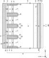
- FIG. 1B shows an example of the aa' cross section in FIG. 1A.
- the aa' cross section is the XZ plane passing through the emitter region 12 in the transistor section 70 .
- the semiconductor device 100 of this example has a semiconductor substrate 10, an interlayer insulating film 38, an emitter electrode 52 and a collector electrode 24 in the aa' section. Emitter electrode 52 is formed above semiconductor substrate 10 and interlayer insulating film 38 .
- the drift region 18 is a first conductivity type region provided in the semiconductor substrate 10 .
- the drift region 18 in this example is of the N ⁇ type as an example.
- Drift region 18 may be a remaining region of semiconductor substrate 10 where no other doping regions are formed. That is, the doping concentration of drift region 18 may be the doping concentration of semiconductor substrate 10 .
- Drift region 18 may be a relatively lightly doped region of semiconductor substrate 10 .
- the drift region 18 may be a region having the lowest acceptor concentration in the P-type region or the lowest donor concentration in the N-type region in the semiconductor substrate 10 excluding the PN junction.
- the doping concentration distribution of the drift region 18 may be substantially uniform along the depth direction of the semiconductor substrate 10 and may have a concentration gradient distribution.
- “Substantially uniform” means that the doping concentration is distributed between 50% and 150% of the average concentration in a region of 30% to 90% of the thickness of the semiconductor substrate 10 in the depth direction. It can mean that there is
- the drift region 18 may be a region in which a depletion layer corresponding to 50% or more of the applied voltage is formed in a state where the depletion layer spreads inside the semiconductor device 100 according to the applied voltage.
- the buffer region 20 is a region of the first conductivity type provided closer to the rear surface 23 of the semiconductor substrate 10 than the drift region 18 is.
- the buffer region 20 of this example is of N type as an example.
- the doping concentration of buffer region 20 is higher than the doping concentration of drift region 18 .
- the buffer region 20 may function as a field stop layer that prevents the depletion layer spreading from the lower surface side of the base region 14 from reaching the collector region 22 of the second conductivity type. Note that the buffer area 20 may be omitted.
- the back side region 60 is provided closer to the back side 23 than the drift region 18 in the semiconductor substrate 10 .
- the back side region 60 may have the first conductivity type or the second conductivity type.
- the back side region 60 in this example has the second conductivity type and functions as the collector region 22, but is not limited to this.
- Backside region 60 may have a higher atomic density than drift region 18 . Atomic density will be described later.
- the upper end of the back side region 60 of this example is in contact with the lower end of the buffer region 20 . When the buffer region 20 is omitted, the upper end of the backside region 60 may contact the lower end of the drift region 18 .
- the back side area 60 will be described later.
- the upper end refers to the end of the semiconductor substrate 10 on the side of the front surface 21 in the depth direction
- the lower end refers to the end of the semiconductor substrate 10 on the side of the back surface 23 in the depth direction. good.
- the upper end and the lower end are not limited to the direction of gravity or the direction when semiconductor device 100 is mounted.
- the collector region 22 is provided below the buffer region 20 in the transistor section 70 .
- Collector region 22 has a second conductivity type.
- the collector region 22 in this example is of P+ type as an example.
- the collector electrode 24 is formed on the back surface 23 of the semiconductor substrate 10 .
- the collector electrode 24 is made of a conductive material such as metal.
- the material of the collector electrode 24 may be the same as or different from the material of the emitter electrode 52 .
- the base region 14 is a second conductivity type region provided above the drift region 18 .
- the base region 14 is provided in contact with the gate trench portion 40 .
- the base region 14 may be provided in contact with the dummy trench portion 30 .
- the emitter region 12 is provided above the base region 14 .
- Emitter region 12 is provided between base region 14 and front surface 21 .
- Emitter region 12 is provided in contact with gate trench portion 40 .
- the emitter region 12 may or may not contact the dummy trench portion 30 .
- the accumulation region 16 is a region of the first conductivity type provided closer to the front surface 21 of the semiconductor substrate 10 than the drift region 18 is.
- the accumulation region 16 of this example is of the N+ type as an example. However, the storage area 16 may not be provided.
- the accumulation region 16 is provided in contact with the gate trench portion 40 .
- the accumulation region 16 may or may not be in contact with the dummy trench portion 30 .
- the doping concentration of accumulation region 16 is higher than the doping concentration of drift region 18 .
- the ion implantation dose for the accumulation region 16 may be 1.0E+12 cm ⁇ 2 or more and 1.0E+13 cm ⁇ 2 or less.
- the ion implantation dose of the accumulation region 16 may be 3.0E+12 cm ⁇ 2 or more and 6.0E+12 cm ⁇ 2 or less.
- E means a power of 10
- 1.0E+12 cm ⁇ 2 means 1.0 ⁇ 10 12 cm ⁇ 2 .
- One or more gate trench portions 40 and one or more dummy trench portions 30 are provided on the front surface 21 .
- Each trench portion extends from the front surface 21 to the drift region 18 .
- each trench portion also penetrates these regions and reaches drift region 18.
- FIG. The fact that the trench penetrates the doping region is not limited to the order of forming the doping region and then forming the trench. A case in which a doping region is formed between the trench portions after the trench portions are formed is also included in the case where the trench portion penetrates the doping region.
- the gate trench portion 40 has a gate trench formed in the front surface 21 , a gate insulating film 42 and a gate conductive portion 44 .
- a gate insulating film 42 is formed to cover the inner wall of the gate trench.
- the gate insulating film 42 may be formed by oxidizing or nitriding the semiconductor on the inner wall of the gate trench.
- the gate conductive portion 44 is formed inside the gate insulating film 42 inside the gate trench.
- the gate insulating film 42 insulates the gate conductive portion 44 from the semiconductor substrate 10 .
- the gate conductive portion 44 is formed of a conductive material such as polysilicon.
- Gate trench portion 40 is covered with interlayer insulating film 38 on front surface 21 .
- the gate conductive portion 44 includes a region facing the adjacent base region 14 on the mesa portion 71 side with the gate insulating film 42 interposed therebetween in the depth direction of the semiconductor substrate 10 .
- a predetermined voltage is applied to the gate conductive portion 44, a channel is formed by an electron inversion layer in the surface layer of the interface of the base region 14 in contact with the gate trench.
- the dummy trench portion 30 may have the same structure as the gate trench portion 40 .
- the dummy trench portion 30 has a dummy trench, a dummy insulating film 32 and a dummy conductive portion 34 formed on the front surface 21 side.
- the dummy insulating film 32 is formed covering the inner wall of the dummy trench.
- the dummy conductive portion 34 is formed inside the dummy trench and inside the dummy insulating film 32 .
- the dummy insulating film 32 insulates the dummy conductive portion 34 from the semiconductor substrate 10 .
- the dummy trench portion 30 is covered with an interlayer insulating film 38 on the front surface 21 .
- the interlayer insulating film 38 is provided above the semiconductor substrate 10 .
- the interlayer insulating film 38 of this example is provided in contact with the front surface 21 .
- An emitter electrode 52 is provided above the interlayer insulating film 38 .
- the interlayer insulating film 38 is provided with one or a plurality of contact holes 54 for electrically connecting the emitter electrode 52 and the semiconductor substrate 10 .
- Contact hole 55 and contact hole 56 may be similarly provided through interlayer insulating film 38 .
- the interlayer insulating film 38 may be a BPSG (boro-phosphosilicate glass) film, a BSG (borosilicate glass) film, a PSG (phosphosilicate glass) film, or an HTO film. or a laminate of these materials.
- the thickness of the interlayer insulating film 38 is, for example, 1.0 ⁇ m, but is not limited to this.
- the first lifetime control region 151 may be provided in the transistor section 70 .
- the first lifetime control area 151 is not essential and may not be provided.
- the first lifetime control region 151 is a region where a lifetime killer is intentionally formed by implanting impurities into the semiconductor substrate 10 or the like. In one example, first lifetime control region 151 is formed by implanting helium into semiconductor substrate 10 . By providing the first lifetime control region 151, it is possible to reduce the turn-off time and suppress the tail current, thereby reducing loss during switching.
- the lifetime killer is the carrier recombination center. Lifetime killers may be lattice defects. For example, lifetime killers may be vacancies, double vacancies, complex defects between these and elements constituting the semiconductor substrate 10, or dislocations. Also, the lifetime killer may be a rare gas element such as helium or neon, or a metal element such as platinum. An electron beam may be used to form lattice defects.
- the lifetime killer concentration is the recombination center concentration of carriers.
- the lifetime killer concentration may be the concentration of lattice defects.
- the lifetime killer concentration may be the concentration of vacancies such as vacancies and double vacancies, the concentration of complex defects between these vacancies and elements constituting the semiconductor substrate 10, or the concentration of dislocations. It's okay.
- the lifetime killer concentration may be the chemical concentration of rare gas elements such as helium and neon, or the chemical concentration of metal elements such as platinum.
- the first lifetime control region 151 is provided closer to the rear surface 23 than the center of the semiconductor substrate 10 in the depth direction of the semiconductor substrate 10 .
- the first lifetime control area 151 of this example is provided in the buffer area 20 .
- the first lifetime control region 151 of this example is provided on the entire surface of the semiconductor substrate 10 in the XY plane, and can be formed without using a mask.
- the first lifetime control region 151 may be provided in part of the semiconductor substrate 10 in the XY plane.
- the impurity dose for forming the first lifetime control region 151 is 5.0E+10 cm ⁇ 2 or more and 5.0E+11 cm ⁇ 2 or less even if it is 0.5E+10 cm ⁇ 2 or more and 1.0E+13 cm ⁇ 2 or less. There may be.
- the first lifetime control region 151 of this example is formed by injection from the back surface 23 side. Thereby, the influence on the front surface 21 side of the semiconductor device 100 can be avoided.
- the first lifetime control region 151 is formed by irradiating helium from the rear surface 23 side.
- whether the first lifetime control region 151 is formed by injection from the front surface 21 side or by injection from the back surface 23 side is mainly determined by the SR method or leakage current measurement. It can be determined by acquiring the state of the front surface 21 side.
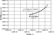
- FIG. 2A is an example of a graph showing the atomic density distribution of the back side region 60.
- the vertical axis indicates atomic density (atoms/cm 3 ), and the horizontal axis indicates analysis depth ( ⁇ m) from the rear surface 23 .
- the atomic density unit may be abbreviated as (cm ⁇ 3 ).
- the back side region 60 of this example functions as the collector region 22 .
- the atomic density of boron which is the dopant of the back side region 60
- the back side region 60 has a gentle slope region 61 , a steep slope region 62 , a peak region 63 and a decrease region 64 .
- the atomic density of the dopant may be simply referred to as atomic density.
- the gentle slope region 61 is a region where the atomic density increases from the back surface 23 side toward the front surface 21 side of the semiconductor substrate 10 in the depth direction of the semiconductor substrate 10 .
- the atomic density gradient of the gentle gradient region 61 may be constant or variable. As will be described later, depending on the characteristics of the analysis means, there may be a region where the atomic density is not measured near the back surface 23 or a region where the atomic density sharply decreases toward the back surface 23 side. As for the region where the atomic density is not measured or the region where the atomic density drops sharply, the gentle gradient region 61 may also be the region where the measured value is interpolated by extrapolation or the like.
- the steep region 62 is provided closer to the front surface 21 than the gentle slope region 61 and is a region where the atomic density increases with a greater gradient than the gentle slope region 61 .
- the steep region 62 is provided closer to the front surface 21 than the gentle region 61 in the depth direction of the semiconductor substrate 10 .
- the peak region 63 is provided closer to the front surface 21 than the steep slope region 62 and has a peak 65 where the atomic density distribution has the maximum value within the range of the back surface region 60 .
- the peak region 63 is provided closer to the front surface 21 than the steep region 62 in the depth direction of the semiconductor substrate 10 .
- the peak region 63 is provided between the steep region 62 and the decreasing region 64 in the depth direction of the semiconductor substrate 10 .
- Np is the peak atomic density of peak 65;
- the peak atomic density Np of the peak 65 may be 1.0E+16 cm ⁇ 3 or more, 1.0E+17 cm ⁇ 3 or more, or 1.0E+18 cm ⁇ 3 or more in the collector region 22 .
- the peak atomic density Np of peak 65 may be 1.0E+20 cm ⁇ 3 or less, 5.0E+19 cm ⁇ 3 or less, 1.0E+19 cm ⁇ 3 or less, 5.0E+18 cm -3 or less.
- the peak atomic density Np of peak 65 in this example is 7.45E+18 cm ⁇ 3 .
- Xp is the depth position of the peak 65 from the back surface 23 in the depth direction of the semiconductor substrate 10 .
- Xp may be 0.1 ⁇ m or more, 0.2 ⁇ m or more, 0.3 ⁇ m or more, or 0.4 ⁇ m or more in the collector region 22 .
- Xp may be 0.8 ⁇ m or less, 0.6 ⁇ m or less, 0.5 ⁇ m or less, or 0.4 ⁇ m or less in the collector region 22 .
- the reduced region 64 is a region in which the atomic density decreases toward the drift region 18 in the depth direction of the semiconductor substrate 10 .
- a depletion region 64 is provided between the peak region 63 and the drift region 18 . If the semiconductor device 100 includes the buffer region 20 , the reduction region 64 may be provided between the peak region 63 and the buffer region 20 and may be in contact with the buffer region 20 .
- the lower end of the gentle slope region 61 may be the back surface 23 of the semiconductor substrate 10 . That is, the back side region 60 may be provided closest to the back side 23 of the semiconductor substrate 10 .
- the upper end of the gentle slope region 61 may be positioned midway between the back surface 23 and the depth position of the peak 65 of the peak region 63 in the depth direction of the semiconductor substrate 10 . That is, the upper end of the gentle slope region 61 may be positioned at 0.5Xp with respect to the depth position Xp of the peak 65 . Note that the upper end of the gentle slope region 61 may be a position where the atomic density is 0.5 Np with the atomic density Np of the peak 65 as a reference.
- the lower end of the steep slope region 62 may be at the same position as the upper end of the gentle slope region 61 in the depth direction of the semiconductor substrate 10 . That is, the lower end of the steep slope region 62 may be at a position of 0.5Xp with the depth position Xp of the peak 65 as a reference.
- the upper end of the steep region 62 may be at the same position as the lower end of the peak region 63 in the depth direction of the semiconductor substrate 10 . As will be described later, the upper end of the steep slope region 62 may be a position where the atomic density is 0.95 Np on the rear surface 23 side of the peak 65 .
- the lower end of the peak region 63 may be a position where the atomic density at the peak 65 is 95% on the back surface 23 side of the semiconductor substrate 10 with respect to the peak 65 . That is, the lower end of the peak region 63 may be positioned closer to the rear surface 23 than the peak 65 and at which the atomic density is 0.95 Np.
- the upper end of the peak region 63 may be a position where the atomic density at the peak 65 is 95% on the front surface 21 side of the semiconductor substrate 10 with respect to the peak 65 . In other words, the upper end of the peak region 63 may be positioned closer to the front surface 21 than the peak 65 at which the atomic density is 0.95 Np.
- the upper end and the lower end of the peak region 63 may be positions where the atomic density is 0.90 Np.
- the lower end of the peak region 63 may be positioned at 0.9Xp with the depth position Xp of the peak 65 as a reference.
- the upper end of the peak region 63 may be a position that is 1.1Xp with the depth position Xp of the peak 65 as a reference.
- the lower end of the reduced region 64 may be at the same position as the upper end of the peak region 63 in the depth direction of the semiconductor substrate 10 . That is, the lower end of the reduced region 64 may be located at a position closer to the front surface 21 than the peak 65 and having an atomic density of 0.95 Np.
- the upper end of the reduced region 64 may be located at a position closer to the front surface 21 of the semiconductor substrate 10 than the peak 65 and having a density of 10% of the atomic density at the peak 65 . That is, the upper end of the peak region 63 may be a position where the atomic density is 0.1 Np on the front surface 21 relative to the peak 65 .
- the gentle slope region 61, the steep slope region 62, the peak region 63, and the decrease region 64 may be continuously provided in order from the back side 23 side. That is, the upper end of the gentle slope region 61 may contact the lower end of the steep slope region 62 . The upper end of steep region 62 may meet the lower end of peak region 63 . The top of peak region 63 may meet the bottom of depletion region 64 .
- the semiconductor device 100 may have a boundary A between the gentle slope region 61 and the steep slope region 62, a boundary B between the steep slope region 62 and the peak region 63, and a peak region 63 and a decreasing slope region 63.
- the atomic density distribution from the gentle gradient region 61 to the steep gradient region 62 may increase continuously. This may allow the electrical activation rate of the dopant to be relatively high.
- the atomic density distribution from the gentle gradient region 61 to the steep gradient region 62 may have a region where the atomic density is partially continuously decreasing, and the atomic density is partially continuously flatly distributed. may have parts.
- the atomic density is partially continuously and flatly distributed means that in a range narrower than the gentle slope region 61 or the steep slope region 62, the maximum and minimum values of the atomic density are the average value of the atomic density in the range may mean within 15% of
- the region be an intermediate region 68 .
- the upper end of the gentle slope area 61 may be positioned anywhere in the intermediate area 68 .
- the upper end of the gentle gradient region 61 may be the upper end of a region where the atomic density distribution has a relatively low density gradient on the back surface 23 side of the depth position Xp of the peak 65 .
- the lower end of the steep region 62 may be the lower end of the region where the density gradient of the atomic density distribution is relatively high on the rear surface 23 side of the depth position Xp of the peak 65 .
- the upper end of the gentle slope region 61 or the lower end of the steep slope region 62 in this case may be located in the middle region 68 .
- the back side region 60 of this example functions as the collector region 22 .
- the position of the peak 65 is separated from the back surface 23 and a gentle slope region 61 and a steep slope region 62 are provided between the back surface 23 and the peak region 63 .
- the peak region 63 and the reduced region 64 can be formed at a depth of 0.2 ⁇ m or more from the back surface 23 .
- the injection efficiency of charge carriers may depend on the magnitude of the atomic density of peak 65 and the magnitude of the gradient of depletion region 64 .
- the doping concentration may be of the same order as the atomic density.
- the depth of the scratch is in the range up to the lower end of the peak region 63 (for example, about 0.3 ⁇ m).
- the charge carrier injection efficiency can be made less sensitive to the depth of the flaw.
- the contact resistance between the backside region 60 and the electrode (collector electrode 24 in this example) formed on the backside 23 is sufficient if the dopant atomic density on the backside 23 is 1 ⁇ 10 18 (atoms/cm 3 ) or more.
- the atomic density of the dopant on the back surface 23 may be maximized when the back surface region 60 is formed as deep as 0.3 ⁇ m or more, for example.
- the gradient of the atomic density is relatively gentle and may not allow for high efficiency of charge carrier injection.
- the back surface side region 60 includes the gentle slope region 61 and the steep slope region 62, the peak region 63 and the decrease region 64 can be formed at a depth position away from the back surface 23, and the atomic density in the decrease region 64 can be reduced. You can make the slope steeper. As a result, not only can the charge carrier injection efficiency be increased, but also the effect of scratches formed on the back surface 23 can be reduced. In this way, the back side region 60 of this example not only can promote carrier injection by having the peak region 63 and the decrease region 64, but also has the gentle slope region 61 and the steep slope region 62. It is also possible to make the rear surface 23 less susceptible to scratches.
- the shape of the doping concentration may also be substantially the same. That is, the atomic density distribution of the back side region 60 may be substantially similar to the doping concentration distribution of the back side region 60 . However, not all dopants in the back side region 60 are donors or acceptors, and the doping concentration may be 10% or more and 100% or less of the atomic density. Also, the doping concentration of the peak 65 in the peak region 63 may be 10% or more and 100% or less of the atomic density of the peak 65 .
- FIG. 2B is an example of a graph showing the atomic density gradient of the gentle gradient region 61.
- the unit of the atomic density gradient in this example is (atoms/cm 4 ).
- the unit of atomic density gradient may be abbreviated as (cm ⁇ 4 ).
- the unit of the atomic density gradient when the description of the unit is omitted, the unit of the atomic density gradient is (atoms/cm 4 ).
- the common logarithm of atomic density may be used to calculate the atomic density gradient.
- the unit of atomic density gradient when using the common logarithm of atomic density may be (/cm). In this specification, the description of the unit of the value of the atomic density gradient may be omitted.
- the unit of the atomic density gradient in this case is (atoms/cm 4 ).
- This figure shows the atomic density gradient a1 of the gentle gradient region 61 of FIG. 2A.
- the atomic density gradient a1 of the gentle gradient region 61 may be 1.0E21 or more, 5.0E21 or more, 1.0E22 or more, or 2.0E22 or more. good.
- the atomic density gradient a1 of the gentle gradient region 61 may be 5.0E23 or less, 2.0E23 or less, 1.0E23 or 8.0E22 or less, 5 .0E22 or less.
- the atomic density gradient a1 in this example is 4.079E+22.
- the atomic density gradient may be calculated by drawing an arbitrary tangent line by fitting the atomic density distribution obtained by measurement, or may be calculated by other methods. In this specification, the atomic density gradient is expressed as an absolute value.
- the average atomic density of the gentle gradient region 61 may be 20% or more, 30% or more, 40% or more, or 50% or more of the peak atomic density Np of the peak 65 .
- the average atomic density of the gentle gradient region 61 may be 95% or less, 90% or less, 85% or less, or 80% or less of the peak atomic density Np of the peak 65, It may be 70% or less.
- the average atomic density of the gentle slope region 61 of this example is about 3.7E+18 atoms/cm 3 , which is about 50% of the peak atomic density Np.
- FIG. 2C is an example of a graph showing the atomic density gradient in the steep region 62.
- FIG. This figure shows the atomic density gradient a2 of the steep region 62 of FIG. 2A.
- the atomic density gradient a2 of the steep region 62 is greater than the atomic density gradient a1 of the gentle region 61.
- FIG. In the collector region 22, the atomic density gradient a2 of the steep region 62 may be 1.0E22 or more, 2.0E22 or more, 5.0E22 or more, or 7.0E22 or more. good.
- the atomic density gradient a2 of the steep region 62 may be 1.0E24 or less, 5.0E23 or less, or 3.0E23 or less.
- the atomic density gradient a2 in this example is 1.680E+23.
- FIG. 2D is an example of a graph showing the atomic density gradient of the depletion region 64.
- FIG. This figure shows the atomic density gradient a3 of the depletion region 64 of FIG. 2A.
- the atomic density gradient a3 is the absolute value of the gradient of the graph of the atomic density distribution in the depletion region 64, so it takes a positive value.
- the atomic density gradient a3 of the depletion region 64 may be 1.0E23 or greater, 2.0E23 or greater, 5.0E23 or greater, or 8.0E23 or greater. .
- the atomic density gradient a3 of the depletion region 64 may be 1.0E25 or less, 8.0E24 or less, 5.0E24 or less, or 3.0E24 or less. .
- the atomic density gradient a3 in this example is 1.618E+24.
- the atomic density at the lower end of the gentle gradient region 61 may be 10% or more and 80% or less of the atomic density Np of the peak 65 .
- the atomic density at the lower end of the gentle slope region 61 may be 30% or more and 60% or less of the atomic density Np of the peak 65 .
- the ratio ⁇ of the atomic density gradient of the gentle region 61 to the atomic density gradient of the steep region 62 may be 0.01 or more and 0.8 or less.
- the atomic density gradient ratio ⁇ may be 0.02 or more, 0.05 or more, or 0.1 or more.
- the atomic density gradient ratio ⁇ may be 0.5 or less, 0.2 or less, or 0.1 or less.
- the ratio ⁇ of the atomic density gradient of the steep region 62 to the atomic density gradient of the decreasing region 64 may be 0.001 or more and 0.5 or less.
- the atomic density gradient ratio ⁇ in the collector region 22 may be 0.005 or more, 0.01 or more, or 0.05 or more.
- the atomic density gradient ratio ⁇ in the collector region 22 may be 0.2 or less, 0.1 or less, or 0.05 or less.
- the semiconductor device 100 having good electrical characteristics while suppressing the influence of scratches on the back surface 23 can be provided.
- FIG. 3A is an example of a top view showing a modification of the semiconductor device 100.
- FIG. FIG. 3A shows the projected position of each member on the upper surface of the semiconductor substrate 10 .
- FIG. 3A only some members of the semiconductor device 100 are shown, and some members are omitted.
- the semiconductor substrate 10 has an edge 102 when viewed from above.
- the semiconductor substrate 10 of this example has two sets of edges 102 facing each other when viewed from above. 3A, the X-axis and Y-axis are parallel to either edge 102. In FIG.
- An active portion 120 is provided on the semiconductor substrate 10 .
- the active portion 120 is a region through which a main current flows in the depth direction between the front surface 21 and the back surface 23 of the semiconductor substrate 10 when the semiconductor device 100 operates.
- An emitter electrode 52 is provided above the active portion 120, but is omitted in FIG. 3A.
- At least one of a transistor section 70 including a transistor element such as an IGBT and a diode section 80 including a diode element such as a freewheeling diode (FWD) is provided in the active section 120 .
- the transistor portions 70 and the diode portions 80 are alternately arranged along a predetermined arrangement direction (the X-axis direction in this example) on the front surface 21 of the semiconductor substrate 10 .
- active portion 120 may include only one of transistor portion 70 and diode portion 80 .
- the region where the transistor section 70 is arranged is denoted by the symbol "I"
- the region where the diode section 80 is arranged is denoted by the symbol "F”.
- the transistor section 70 and the diode section 80 may each have a length in the extending direction. That is, the length in the Y-axis direction of the transistor section 70 is greater than the width in the X-axis direction. Similarly, the length in the Y-axis direction of the diode section 80 is greater than the width in the X-axis direction.
- the extending direction of the transistor portion 70 and the diode portion 80 may be the same as the longitudinal direction of each trench portion described later.
- the diode section 80 has an N+ type cathode region in a region in contact with the back surface 23 of the semiconductor substrate 10 .
- the region provided with the cathode region is referred to as the diode section 80 . That is, the diode portion 80 is a region that overlaps with the cathode region when viewed from above.
- a P+ type collector region 22 may be provided on the back surface 23 of the semiconductor substrate 10 in a region other than the cathode region.
- the diode section 80 may include an extension region 85 extending in the Y-axis direction from the diode section 80 to the gate wiring described later.
- a collector region 22 is provided on the rear surface 23 of the extension region 85 .
- the semiconductor device 100 may have one or more pads above the semiconductor substrate 10 .
- the semiconductor device 100 of this example has a gate pad 112 .
- Semiconductor device 100 may have pads such as an anode pad, a cathode pad, and a current sensing pad. Each pad is arranged near the edge 102 .
- the vicinity of the edge 102 refers to a region between the edge 102 and the emitter electrode 52 in top view.
- each pad may be connected to an external circuit via a wiring such as a wire.
- a gate potential is applied to the gate pad 112 .
- Gate pad 112 is electrically connected to gate conductive portion 44 of gate trench portion 40 of active portion 120 .
- the semiconductor device 100 includes gate wiring that connects the gate pad 112 and the gate trench portion 40 . In FIG. 3A, the gate wiring is hatched with oblique lines.
- the gate wiring of this example has a peripheral gate wiring 130 and an active side gate wiring 131 .
- the peripheral gate wiring 130 and the active side gate wiring 131 are examples of the gate metal layer 50 .
- the peripheral gate wiring 130 is arranged between the active portion 120 and the edge 102 of the semiconductor substrate 10 when viewed from above.
- the peripheral gate wiring 130 of this example surrounds the active portion 120 when viewed from above.
- a region surrounded by the peripheral gate wiring 130 in a top view may be the active portion 120 .
- the peripheral gate wiring 130 is connected to the gate pad 112 .
- the peripheral gate wiring 130 is arranged above the semiconductor substrate 10 .
- the peripheral gate wiring 130 may be a metal wiring containing aluminum or the like.
- the active side gate wiring 131 is provided in the active portion 120 .
- variations in wiring length from the gate pad 112 can be reduced for each region of the semiconductor substrate 10 .
- the active side gate wiring 131 is connected to the gate trench portion of the active portion 120 .
- the active-side gate wiring 131 is arranged above the semiconductor substrate 10 .
- the active-side gate wiring 131 may be a wiring made of a semiconductor such as polysilicon doped with impurities.
- the active side gate wiring 131 may be connected to the peripheral gate wiring 130 .
- the active-side gate wiring 131 of this example is provided extending in the X-axis direction so as to cross the active portion 120 from one outer peripheral gate wiring 130 to the other outer peripheral gate wiring 130 at approximately the center in the Y-axis direction. there is When the active portion 120 is divided by the active-side gate wiring 131, the transistor portions 70 and the diode portions 80 may be alternately arranged in the X-axis direction in each divided region.
- the semiconductor device 100 also includes a temperature sensing portion (not shown), which is a PN junction diode made of polysilicon or the like, and a current detecting portion (not shown) that simulates the operation of a transistor portion provided in the active portion 120. good too.
- a temperature sensing portion which is a PN junction diode made of polysilicon or the like
- a current detecting portion (not shown) that simulates the operation of a transistor portion provided in the active portion 120. good too.
- the edge termination structure 140 is provided on the front surface 21 of the semiconductor substrate 10 .
- the edge termination structure portion 140 is provided between the active portion 120 and the edge 102 in top view.
- the edge termination structure 140 in this example is arranged between the peripheral gate line 130 and the edge 102 .
- the edge termination structure 140 relaxes electric field concentration on the front surface 21 side of the semiconductor substrate 10 .
- the edge termination structure 140 may comprise at least one of a guard ring, a field plate and a resurf annularly surrounding the active portion 120 .
- FIG. 3B is an enlarged view of area A in FIG. 3A.
- Region A is a region including transistor portion 70 and diode portion 80 .
- the semiconductor device 100 of this example includes a gate trench portion 40 , a dummy trench portion 30 , an emitter region 12 , a base region 14 , a contact region 15 and a well region 17 provided inside the upper surface side of the semiconductor substrate 10 .
- Each of the gate trench portion 40 and the dummy trench portion 30 is an example of the trench portion.
- the dummy trench portion 30 of this example may have a U-shape on the front surface 21 of the semiconductor substrate 10 in the same manner as the gate trench portion 40 . That is, the dummy trench portion 30 may have two extending portions 31 extending along the extending direction and a connection portion 33 connecting the two extending portions 31 .
- the semiconductor device 100 of this example includes an emitter electrode 52 and a gate metal layer 50 provided above the front surface 21 of the semiconductor substrate 10 . Emitter electrode 52 and gate metal layer 50 are provided separately from each other.
- the transistor portion 70 of this example includes a boundary portion 90 located at the boundary between the transistor portion 70 and the diode portion 80 .
- the boundary portion 90 is a region provided in the transistor portion 70 and adjacent to the diode portion 80 .
- Boundary 90 has contact region 15 .
- the border 90 in this example does not have an emitter region 12 .
- the trench portion of boundary portion 90 is dummy trench portion 30 .
- the boundary portion 90 of this example is arranged so that both ends thereof in the X-axis direction are the dummy trench portions 30 .
- Boundary 90 is not essential and may not be provided.
- the contact hole 54 is provided above the base region 14 in the diode section 80 .
- Contact hole 54 is provided above contact region 15 at boundary portion 90 . None of the contact holes 54 are provided above the well regions 17 provided at both ends in the Y-axis direction.
- the mesa portion 91 is provided at the boundary portion 90 .
- the mesa portion 91 has a contact region 15 on the front surface 21 of the semiconductor substrate 10 .
- the mesa portion 91 of this example has the base region 14 and the well region 17 on the negative side in the Y-axis direction.
- the mesa portion 81 is provided in a region sandwiched between adjacent dummy trench portions 30 in the diode portion 80 .
- Mesa portion 81 has base region 14 on front surface 21 of semiconductor substrate 10 .
- the mesa portion 81 may have a contact region 15 on the front surface 21 of the semiconductor substrate 10 .
- the mesa portion 81 of this example has the base region 14 and the well region 17 on the negative side in the Y-axis direction.
- the emitter region 12 is provided in the mesa portion 71, it may not be provided in the mesa portion 81 and the mesa portion 91.
- the contact region 15 is provided on the mesa portion 71 and the mesa portion 91 , but may not be provided on the mesa portion 81 .
- FIG. 3C shows a bb' cross section of a modified example of the semiconductor device 100.
- FIG. This figure corresponds to the bb' section of FIG. 3B.
- the semiconductor device 100 of this example includes a first lifetime control region 151 and a second lifetime control region 152 .
- the first lifetime control area 151 and the second lifetime control area 152 are not essential and may not be provided.
- the contact region 15 is provided above the base region 14 in the mesa portion 91 .
- the contact region 15 is provided in contact with the dummy trench portion 30 in the mesa portion 91 .
- the contact region 15 may be provided on the front surface 21 of the mesa portion 71 .
- the accumulation region 16 is provided in the transistor section 70 and the diode section 80 .
- the accumulation region 16 of this example is provided over the entire surfaces of the transistor section 70 and the diode section 80 .
- the accumulation region 16 may not be provided in the diode section 80 .
- the cathode region 82 is provided below the buffer region 20 in the diode section 80 .
- the boundary between collector region 22 and cathode region 82 is the boundary between transistor section 70 and diode section 80 . That is, the collector region 22 is provided below the boundary portion 90 in this example.
- the first lifetime control region 151 is provided in both the transistor section 70 and the diode section 80. As a result, the semiconductor device 100 of this example can speed up the recovery in the diode section 80 and further improve the switching loss.
- the first lifetime control region 151 may be formed by a method similar to that of the first lifetime control region 151 of other embodiments.
- the second lifetime control region 152 is provided closer to the front surface 21 than the center of the semiconductor substrate 10 in the depth direction of the semiconductor substrate 10 .
- the second lifetime control region 152 of this example is provided in the drift region 18 .
- Second lifetime control region 152 is provided in both transistor section 70 and diode section 80 .
- the second lifetime control region 152 may be formed by implanting impurities from the front surface 21 side, or may be formed by implanting impurities from the back surface 23 side.
- the second lifetime control region 152 is provided between the diode section 80 and the boundary section 90 , and may not be provided in part of the transistor section 70 .
- the second lifetime control area 152 may be formed by any method among the methods for forming the first lifetime control area 151 .
- the elements and doses for forming the first lifetime control region 151 and the second lifetime control region 152 may be the same or different.
- FIG. 4A is an example of a graph showing the atomic density distribution of the back side region 60.
- the vertical axis indicates atomic density (atoms/cm 3 ), and the horizontal axis indicates analysis depth ( ⁇ m).
- the back side region 60 of this example functions as a cathode region 82 .
- the atomic density of phosphorus which is the dopant of the back side region 60, is shown.
- the back side region 60 has a gentle slope region 61 , a steep slope region 62 , a peak region 63 and a decrease region 64 .
- Np in this example is the atomic density of peak 65 in cathode region 82 .
- the atomic density Np of the peak 65 may be 1.0E+18 cm ⁇ 3 or more, 5.0E+18 cm ⁇ 3 or more, or 1.0E+19 cm ⁇ 3 or more in the cathode region 82 .
- the atomic density Np of peak 65 may be 1.0E21 cm ⁇ 3 or less, 5.0E+21 cm ⁇ 3 or less, or 1.0E+20 cm ⁇ 3 or less in cathode region 82 .
- the atomic density Np of peak 65 in this example is 1.43E+20 cm ⁇ 3 .
- Xp may be 0.1 ⁇ m or more, 0.2 ⁇ m or more, or 0.3 ⁇ m or more in the cathode region 82 .
- Xp may be 0.8 ⁇ m or less, 0.6 ⁇ m or less, or 0.4 ⁇ m or less in the cathode region 82 .
- the back side region 60 of this example functions as a cathode region 82, and the atomic density distribution as in this example makes it easier to inject carriers.
- making the depletion region 64 steep makes it easier to inject carriers.
- holes can be easily injected when the diode is turned on, and the on-characteristics of the semiconductor device 100 can be improved.
- FIG. 4B is an example of a graph showing the atomic density gradient of the gentle gradient region 61.
- FIG. This figure shows the atomic density gradient a1 of the gentle gradient region 61 of FIG. 4A.
- the atomic density gradient a1 of the gentle gradient region 61 may be 1.0E22 or more, 3.0E22 or more, 5.0E22 or more, or 8.0E22 or more. good.
- the atomic density gradient a1 of the gentle gradient region 61 may be 2.0E24 or less, 1.0E24 or less, 8.0E23 or less, or 5.0E23 or less. good.
- the atomic density gradient a1 in this example is 2.938E+23.
- the average atomic density of the gentle slope region 61 may be 20% or more, 30% or more, 40% or more, or 50% or more of the peak atomic density Np of the peak 65.
- the average atomic density of the gentle gradient region 61 may be 95% or less, 90% or less, 85% or less, or 80% or less of the peak atomic density Np of the peak 65, It may be 70% or less.
- the average atomic density of the gentle gradient region 61 of this example is approximately 1.2E+20 atoms/cm 3 , which is approximately 82% of the peak atomic density Np.
- FIG. 4C is an example of a graph showing the atomic density gradient of the steep region 62.
- FIG. This figure shows the atomic density gradient a2 in the steep region 62 of FIG. 4A.
- the atomic density gradient a2 of the steep region 62 is greater than the atomic density gradient a1 of the gentle region 61.
- FIG. In the cathode region 82, the atomic density gradient a2 of the steep region 62 may be 1.0E23 or greater, 2.0E23 or greater, 5.0E23 or greater, or 8.0E23 or greater. good.
- the atomic density gradient a2 of the steep region 62 may be 1.0E25 or less, may be 8.0E24 or less, may be 5.0E24 or less, or may be 3.0E24 or less. good.
- the atomic density gradient a2 in this example is 2.043E+24.
- FIG. 4D is an example of a graph showing the atomic density gradient of the depletion region 64.
- FIG. This figure shows the atomic density gradient a3 of the depletion region 64 of FIG. 4A.
- the atomic density gradient a3 is the absolute value of the gradient of the graph of the atomic density distribution in the depletion region 64, so it takes a positive value.
- the atomic density gradient a3 of the depletion region 64 may be 2.0E24 or greater, 5.0E24 or greater, 8.0E24 or greater, or 1.0E25 or greater. .
- the atomic density gradient a3 of the depletion region 64 may be 2.0E26 or less, 1.0E26 or less, 8.0E25 or less, or 5.0E25 or less. .
- the atomic density gradient a3 in this example is 2.392E+25.
- the atomic density at the lower end of the gentle gradient region 61 may be 30% or more and 90% or less of the atomic density Np of the peak 65 .
- the atomic density at the lower end of the gentle slope region 61 may be 50% or more and 80% or less of the atomic density Np of the peak 65 .
- the ratio ⁇ of the atomic density gradient of the gentle region 61 to the atomic density gradient of the steep region 62 may be 0.01 or more and 0.5 or less.
- the atomic density gradient ratio ⁇ may be 0.02 or more, 0.05 or more, or 0.1 or more.
- the atomic density gradient ratio ⁇ in the cathode region 82 may be 0.3 or less, 0.2 or less, or 0.1 or less.
- the ratio ⁇ of the atomic density gradient of the steep region 62 to the atomic density gradient of the declining region 64 may be 0.001 or more and 0.3 or less.
- the atomic density gradient ratio ⁇ in the cathode region 82 may be 0.005 or more, 0.01 or more, or 0.05 or more.
- the atomic density gradient ratio ⁇ in the cathode region 82 may be 0.2 or less, 0.1 or less, or 0.08 or less.
- the back side region 60 of this example functions as a cathode region 82 .
- the position of the peak 65 is separated from the back surface 23 and a gentle slope region 61 and a steep slope region 62 are provided between the back surface 23 and the peak region 63 .
- the peak region 63 and the reduced region 64 can be formed at a depth of 0.1 ⁇ m or more from the back surface 23 .
- the injection efficiency of charge carriers may depend on the magnitude of the atomic density of peak 65 and the magnitude of the gradient of depletion region 64 .
- the doping concentration may be of the same order as the atomic density.
- the depth of the scratch is in the range up to the lower end of the peak region 63 (for example, about 0.2 ⁇ m).
- the charge carrier injection efficiency can be made less sensitive to the depth of the flaw.
- an increase in forward voltage drop due to scratches on the back surface 23 can be suppressed.
- the contact resistance between the backside region 60 and the backside electrode (collector electrode 24 in this example) formed on the backside 23 is sufficient if the dopant atomic density on the backside 23 is 1 ⁇ 10 18 (atoms/cm 3 ) or more. .
- the dopant atomic density on the back surface 23 may be maximized when the back surface region 60 is formed as deep as 0.2 ⁇ m or more, for example.
- the gradient of the atomic density is relatively gentle and may not allow for high efficiency of charge carrier injection.
- the back surface side region 60 includes the gentle slope region 61 and the steep slope region 62, the peak region 63 and the decrease region 64 can be formed at a depth position away from the back surface 23, and the atomic density in the decrease region 64 can be reduced. You can make the slope steeper. As a result, not only can the charge carrier injection efficiency be increased, but also the effect of scratches formed on the back surface 23 can be reduced. In this way, the back side region 60 of this example not only can promote carrier injection by having the peak region 63 and the decrease region 64, but also has the gentle slope region 61 and the steep slope region 62. It is also possible to make the rear surface 23 less susceptible to scratches.
- the depletion layer may reach the cathode region 82. Leakage current increases when the depletion layer reaches the back electrode. In order to prevent the depletion layer from reaching the back electrode, the doping concentration of the cathode region 82, that is, the atomic density of the dopant in the cathode region 82 is increased so that the depletion layer stops inside the cathode region 82 and reaches the back electrode. It is possible to prevent it from reaching. On the other hand, when back surface 23 is scratched as described above, the depletion layer may reach the back surface electrode at the scratch on back surface 23 , thereby increasing leakage current.
- the atomic density of the cathode region 82 is relatively low at the tip of the flaw on the front surface 21 side. Therefore, the depletion layer easily reaches the back electrode at the scratch on the back surface 23 .
- the position of the peak 65 is separated from the rear surface 23, and the gentle slope region 61 and the steep slope region 62 are provided between the rear surface 23 and the peak region 63. 63 or steep region 62 can be deepened. As a result, the depletion layer is stopped in the peak region 63, the steep slope region 62, or the gentle slope region 61, and an increase in leakage current can be suppressed.
- the back side region 60 of this example functions as a cathode region 82 and can stop the depletion layer at a peak 65 away from the back side 23. Therefore, even if the back side 23 is scratched, the damage will not occur. If the depth is in the range from the gentle gradient region 61 to the steep gradient region 62, for example, it is possible to suppress an increase in leakage current due to scratches on the back surface 23.
- FIG. 5 is a flowchart showing an example of the manufacturing process of the semiconductor device 100.
- step S100 the structure on the front surface 21 side of the semiconductor device 100 is formed.
- step S100 after the structure on the front surface 21 side is formed, the back surface 23 side of the semiconductor substrate 10 is ground, and the thickness of the semiconductor substrate 10 is adjusted according to the required electrical characteristics such as withstand voltage. to adjust.
- a dopant is ion-implanted to form the back surface region 60 from the back surface 23 side of the semiconductor substrate 10 .
- the back surface side region 60 may be formed on the entire surface of the back surface 23 of the semiconductor substrate 10 . If backside region 60 is collector region 22, the dopant may be boron. If backside region 60 is cathode region 82, the dopant may be phosphorus. If the back side region 60 includes both the collector region 22 and the cathode region 82, the dopants for the collector region 22 and the cathode region 82 may be ion-implanted separately in each region.
- the dopant dose for forming the collector region 22 may be 2.0E+13 cm ⁇ 2 or more and may be 5.0E+13 cm ⁇ 2 or less.
- the dopant dose for forming the cathode region 82 may be greater than or equal to 1.0E14 cm ⁇ 2 and less than or equal to 1.0E16 cm ⁇ 2 .
- Acceleration energy of ion implantation for forming back side region 60 may be 10 keV or more and 300 keV or less in collector region 22 or cathode region 82 .
- step S104 the semiconductor substrate 10 is laser annealed from the back surface 23 side of the semiconductor substrate 10.
- the dopant ion-implanted region of the back side region 60 is laser annealed.
- Laser annealing selectively heats the region into which the dopant is ion-implanted from the back surface 23 side of the semiconductor substrate 10 .
- the back side region 60 having the peak 65 can be formed.
- each region of the collector region 22 and the cathode region 82 may be laser annealed simultaneously or separately.
- the peak position of the dopant for forming the back side region 60 can be changed. As a result, a gentle gradient region 61, a steep gradient region 62, a peak region 63 and a decreasing region 64 are formed.
- the type of laser used for annealing the back side region 60 is not particularly limited.
- the laser used for annealing the back side region 60 may be a XeCl excimer laser (wavelength 308 nm), a KrF excimer laser (wavelength 248 nm), or a XeF excimer laser (wavelength 351 nm).
- YAG2 ⁇ second harmonic of YAG
- YAG3 ⁇ third harmonic of YAG
- the type of laser used for annealing the back side region 60 may be a laser with a penetration depth of laser light of, for example, 5 ⁇ m or less.
- the step for forming the back side region 60 does not need to include thermal annealing for forming the back side region 60 . That is, defect recovery and dopant activation in the back side region 60 may be realized only by laser annealing. However, defect recovery and dopant activation in the back side region 60 may be realized by using thermal annealing in addition to laser annealing. Thermal annealing may be furnace annealing in which the semiconductor device 100 is heated in a furnace.
- a backside electrode is formed.
- the backside electrode may be the collector electrode 24 or the cathode electrode.
- the backside electrode is formed by a sputtering method.
- the backside electrode may be a laminated electrode in which an aluminum layer, a titanium layer, a nickel layer, and the like are laminated.
- FIG. 6 shows the atomic density distribution before and after laser annealing of the back side region 60 .
- the vertical axis indicates the atomic density (atoms/cm 3 ) and the secondary ion intensity of silicon (arb.Unit), and the horizontal axis indicates the analysis depth ( ⁇ m) from the rear surface 23 .
- the solid line shows the atomic density distribution of the back side region 60 during ion implantation and after laser annealing.
- the dopant for the backside region 60 in this example is boron.
- the atomic density distribution has a peak at the depth of the range Rp.
- the time of ion implantation may be a stage after dopant ion implantation of the back side region 60 and before annealing of the back side region 60 .
- the depth position Xp of the peak 65 after laser annealing is larger than the range Rp of the peak during ion implantation.
- the peak of the atomic density distribution is reproduced at a position closer to the front surface 21 of the semiconductor substrate 10 than the peak position of the atomic density distribution after ion implantation. distributed.
- the depth position of the semiconductor substrate 10 melted by laser annealing may be appropriately changed according to the atomic density distribution or material of the back side region 60 .
- the irradiation depth of laser annealing particularly the melting depth due to laser annealing, may include a region from the back surface 23 of the semiconductor substrate 10 to the range Rp of the peak during ion implantation, and the depth position Xp of the peak 65 from the back surface 23 may be included. up to and including the entire region where the back side region 60 is formed. That is, the melting depth may be equal to or greater than the range Rp of the peak during ion implantation.
- Laser irradiation is performed by placing the semiconductor substrate 10 horizontally with the laser irradiation surface (back surface 23 in this example) facing upward among the main surfaces of the semiconductor substrate 10 in a wafer state.
- the melting depth By setting the melting depth to be equal to or greater than the peak range Rp during ion implantation, 50% or more of the total amount of the implanted dopant can be placed inside the melted semiconductor material. This causes the atomic density of the implanted dopants to be substantially uniformly redistributed over the range of melt depths.
- the dopant precipitates along the gravity on the side of the installation surface (the front surface 21 in this example), which is the main surface opposite to the irradiation surface, within the range of the melting depth.
- the peak position of the dopant atom density distribution moves to the range Rp of the peak during ion implantation or deeper. Furthermore, due to the movement of the dopant, a gentle slope region 61, a steep slope region 62, a peak region 63 and a decrease region 64 are formed in order from the back surface 23 side toward the front surface 21 side.
- the laser annealing conditions for example, laser beam intensity, irradiation time, number of irradiation times and time intervals, overlap ratio, etc.
- the back side region 60 having a gentle slope region 61, a steep slope region 62, a peak region 63 and a decrease region 64 can be formed.
- the dashed-dotted line graph shows the measurement results of the secondary ion intensity of silicon, which is the semiconductor substrate 10 .
- the measurement results are not stable, and the secondary ion intensity of silicon is not accurately measured. That is, the dopant atomic density of the back side region 60 may not be accurately measured. Therefore, in the region near the back surface 23, the measured value of the atomic density of the back surface side region 60 may be interpolated by extrapolation or the like.
- the integrated density of the back side region 60 may be reduced by irradiation with laser annealing.
- the ratio of the integrated concentration of the back side region 60 after laser annealing to the integrated concentration of the back side region 60 before laser annealing may be 85% or more, 90% or more, or 95%. or more.
- the ratio of the integrated concentration of the back side region 60 after laser annealing to the integrated concentration of the back side region 60 before laser annealing may be less than 100%, may be 99% or less, and may be 95%. % or less.
- the ratio of integrated densities in this example is 97%. The same applies when the dopant is phosphorus or arsenic.
- FIG. 7 shows the measurement results of the atomic density on the back surface 23 side of the semiconductor substrate 10 .
- This figure shows the analysis results of secondary ions measured by SIMS.
- the back side region 60 has a gentle slope region 61, a steep slope region 62, a peak region 63 and a decrease region 64, as shown in other examples.
- FIG. 8 shows the measurement results of the doping concentration on the back surface 23 side of the semiconductor substrate 10 .
- the dopant is boron
- an example of distribution of doping concentration (net doping concentration, carrier concentration) measured by the SR method is shown.
- the dopant is not limited to boron, and may be phosphorus or arsenic.
- the doping concentration distribution measured by the SR method also reflects the same characteristics as the SIMS analysis result of the back side region 60 shown in FIG. That is, the atomic density distribution of the back side region 60 may be substantially similar to the doping concentration distribution of the back side region 60 .
- the doping concentration distribution measured by the SR method may have small fluctuations in a plurality of measured values due to the spreading resistance measurement environment such as errors.
- the semiconductor device 100 has a doping gentle gradient region 161 with a doping concentration distribution corresponding to the gentle gradient region 61 of the atomic density distribution, and a doping steep region 161 with a doping concentration distribution corresponding to the steep gradient region 62 of the atomic density distribution.
- NDp is the peak doping concentration of doping peak 165
- X Dp is the depth position of the doping peak 165 from the back surface 23 in the depth direction of the semiconductor substrate 10 .
- the reduced doping region 164 may be a region in which the doping concentration decreases from the back surface 23 toward the drift region 18 in the depth direction of the semiconductor substrate 10 .
- a doping reduction region 164 is provided between the doping peak region 163 and the drift region 18 . If semiconductor device 100 includes buffer region 20 , reduced doping region 164 may be provided between doping peak region 63 and buffer region 20 and may contact buffer region 20 .
- the lower end of the gently doped region 161 may be the back surface 23 of the semiconductor substrate 10 .
- the upper end of the gently doped region 161 may be located midway between the back surface 23 and the depth position of the doping peak 165 of the doping peak region 163 in the depth direction of the semiconductor substrate 10 . That is, the upper end of the gentle doping gradient region 161 may be positioned at 0.5X Dp with respect to the depth position X Dp of the doping peak 165 .
- the upper end of the doping gentle gradient region 161 may be a position where the doping concentration is 0.5N Dp with the doping concentration N Dp of the doping peak 165 as a reference.
- the depth range of the gently doped region 161 may be the same depth range as the gently doped region 61 .
- the lower end of the steep doping region 162 may be at the same position as the upper end of the gentle doping region 161 in the depth direction of the semiconductor substrate 10 . That is, the lower end of the steep doping region 162 may be 0.5X Dp with respect to the depth position X Dp of the doping peak 165 .
- the upper end of the doping steep region 162 may be at the same position as the lower end of the doping peak region 163 in the depth direction of the semiconductor substrate 10 .
- the upper end of the steep doping region 162 may be located at a doping concentration of 0.95 N Dp on the back surface 23 side of the doping peak 165, as described below.
- the depth range of doping steep region 162 may be the same depth range as steep region 62 .
- the lower end of the doping peak region 163 may be located on the back surface 23 side of the semiconductor substrate 10 with respect to the doping peak 165 and at a doping concentration of 95% of the doping peak 165 . That is, the lower end of the doping peak region 163 may be positioned closer to the rear surface 23 than the doping peak 165 and at a doping concentration of 0.95 N Dp .
- the upper end of the doping peak region 163 may be located on the front surface 21 side of the semiconductor substrate 10 with respect to the doping peak 165 and at a doping concentration of 95% of the doping peak 165 .
- the upper end of the doping peak region 163 may be located at a position where the doping concentration is 0.95N Dp on the front surface 21 side of the doping peak 165 . Also, the upper end and the lower end of the doping peak region 163 may each have a doping concentration of 0.90N Dp . Note that the lower end of the doping peak region 163 may be positioned at 0.9X Dp with the depth position X Dp of the doping peak 165 as a reference. The upper end of the doping peak region 163 may be 1.1X Dp with respect to the depth position X Dp of the doping peak 165 . Alternatively, the depth range of doping peaks 165 may be the same depth range as peak region 63 .
- the lower end of the doping decrease region 164 may be at the same position as the upper end of the doping peak region 163 in the depth direction of the semiconductor substrate 10 . That is, the lower end of the doping reduction region 164 may be located at a position where the doping concentration is 0.95 Np on the front surface 21 side of the doping peak 165 .
- the upper end of the reduced doping region 164 may be located closer to the front surface 21 of the semiconductor substrate 10 than the doping peak 165 and at a density of 10% of the doping concentration at the doping peak 165 . That is, the upper end of the doping peak region 163 may be a position where the atomic density is 0.1 Np on the front surface 21 relative to the doping peak 165 .
- the depth range of reduced doping region 164 may be the same depth range as reduced region 64 .
- the gentle doping region 161, the steep doping region 162, the peak doping region 163, and the reduced doping region 164 may be continuously provided in order from the back side 23 side. That is, the upper end of the gently doped region 161 may contact the lower end of the steeply doped region 162 . The upper end of doping steep region 162 may contact the lower end of doping peak region 163 . The upper end of doping peak region 163 may contact the lower end of doping decreasing region 164 .
- the semiconductor device 100 may have a boundary A D between the gentle doping region 161 and the steep doping region 162 and a boundary B D between the steep doping region 162 and the peak doping region 163 . , may have a boundary C D between the doping peak region 163 and the reduced doping region 164 , and a boundary D D between the reduced doping region 164 and the drift region 18 .
- the doping concentration distribution from the gentle doping gradient region 161 to the steep doping gradient region 162 has a continuous gradient of the doping concentration distribution (doping concentration gradient). may be increased to This may allow the electrical activation rate of the dopant to be relatively high.
- the doping concentration distribution from the gently doped region 161 to the steeply doped region 162 may have a region where the doping concentration decreases partially continuously and the doping concentration flattens out partially continuously. It may have a distributed portion.
- the doping concentration is partially continuous and flatly distributed in any of the gentle gradient region 61, the steep gradient region 62, the gentle doping gradient region 161, or the steep doping gradient region 162, or in a narrower region than the narrowest region.
- the maximum and minimum doping concentrations are within 15% of the average doping concentration in the range.
- Reference Signs List 10 Semiconductor substrate 12 Emitter region 14 Base region 15 Contact region 16 Accumulation region 17 Well region 18 Drift region 20 Buffer region 21 Front surface 22 Collector region 23 Back surface 24 Collector electrode 25 Connection portion 30 Dummy Trench portion 31 Extension portion 32 Dummy insulating film 33 Connection portion 34 Dummy conductive portion 38 Interlayer insulating film 40 Gate trench portion 41 Extension portion 42 Gate insulating film 43 Connection portion 44 Gate conductive portion 50 Gate metal layer 52 Emitter electrode 54 Contact hole , 55...contact hole, 56...contact hole, 60...back side area, 61...slow slope area, 62...steep slope area, 63...peak area, 64...
Landscapes
- Metal-Oxide And Bipolar Metal-Oxide Semiconductor Integrated Circuits (AREA)
- Electrodes Of Semiconductors (AREA)
- Bipolar Transistors (AREA)
- Physics & Mathematics (AREA)
- Electromagnetism (AREA)
- Optics & Photonics (AREA)
Priority Applications (4)
| Application Number | Priority Date | Filing Date | Title |
|---|---|---|---|
| JP2024500927A JP7687514B2 (ja) | 2022-02-17 | 2022-06-16 | 半導体装置およびその製造方法 |
| DE112022002851.3T DE112022002851T5 (de) | 2022-02-17 | 2022-06-16 | Halbleitervorrichtung und verfahren für dessen herstellung |
| CN202280051893.5A CN117836952A (zh) | 2022-02-17 | 2022-06-16 | 半导体装置及其制造方法 |
| US18/418,362 US20240162287A1 (en) | 2022-02-17 | 2024-01-22 | Semiconductor device and method for manufacturing the same |
Applications Claiming Priority (2)
| Application Number | Priority Date | Filing Date | Title |
|---|---|---|---|
| JP2022-022803 | 2022-02-17 | ||
| JP2022022803 | 2022-02-17 |
Related Child Applications (1)
| Application Number | Title | Priority Date | Filing Date |
|---|---|---|---|
| US18/418,362 Continuation US20240162287A1 (en) | 2022-02-17 | 2024-01-22 | Semiconductor device and method for manufacturing the same |
Publications (1)
| Publication Number | Publication Date |
|---|---|
| WO2023157330A1 true WO2023157330A1 (ja) | 2023-08-24 |
Family
ID=87577842
Family Applications (1)
| Application Number | Title | Priority Date | Filing Date |
|---|---|---|---|
| PCT/JP2022/024121 Ceased WO2023157330A1 (ja) | 2022-02-17 | 2022-06-16 | 半導体装置およびその製造方法 |
Country Status (5)
| Country | Link |
|---|---|
| US (1) | US20240162287A1 (https=) |
| JP (1) | JP7687514B2 (https=) |
| CN (1) | CN117836952A (https=) |
| DE (1) | DE112022002851T5 (https=) |
| WO (1) | WO2023157330A1 (https=) |
Citations (5)
| Publication number | Priority date | Publication date | Assignee | Title |
|---|---|---|---|---|
| JP2007123469A (ja) * | 2005-10-27 | 2007-05-17 | Toyota Central Res & Dev Lab Inc | 半導体装置とその製造方法 |
| WO2014112228A1 (ja) * | 2013-01-18 | 2014-07-24 | 株式会社日立パワーデバイス | ダイオード、電力変換装置 |
| WO2015118713A1 (ja) * | 2014-02-10 | 2015-08-13 | トヨタ自動車株式会社 | 半導体装置及び半導体装置の製造方法 |
| WO2020080295A1 (ja) * | 2018-10-18 | 2020-04-23 | 富士電機株式会社 | 半導体装置および製造方法 |
| WO2021166980A1 (ja) * | 2020-02-18 | 2021-08-26 | 富士電機株式会社 | 半導体装置 |
Family Cites Families (8)
| Publication number | Priority date | Publication date | Assignee | Title |
|---|---|---|---|---|
| JP2996567B2 (ja) * | 1992-10-30 | 2000-01-11 | 松下電子工業株式会社 | 固体撮像素子の製造方法 |
| JP4676708B2 (ja) | 2004-03-09 | 2011-04-27 | 新電元工業株式会社 | 半導体装置の製造方法 |
| JPWO2012056536A1 (ja) | 2010-10-27 | 2014-03-20 | 富士電機株式会社 | 半導体装置および半導体装置の製造方法 |
| JP5621621B2 (ja) | 2011-01-24 | 2014-11-12 | 三菱電機株式会社 | 半導体装置と半導体装置の製造方法 |
| JP5700025B2 (ja) | 2012-11-27 | 2015-04-15 | トヨタ自動車株式会社 | 半導体装置とその製造方法 |
| US9673308B2 (en) | 2013-12-13 | 2017-06-06 | Mitsubishi Electric Corporation | Semiconductor device manufacturing method |
| JP6112071B2 (ja) | 2014-06-19 | 2017-04-12 | トヨタ自動車株式会社 | 半導体装置の製造方法 |
| JP7010184B2 (ja) | 2018-09-13 | 2022-01-26 | 株式会社デンソー | 半導体装置 |
-
2022
- 2022-06-16 DE DE112022002851.3T patent/DE112022002851T5/de active Pending
- 2022-06-16 CN CN202280051893.5A patent/CN117836952A/zh active Pending
- 2022-06-16 WO PCT/JP2022/024121 patent/WO2023157330A1/ja not_active Ceased
- 2022-06-16 JP JP2024500927A patent/JP7687514B2/ja active Active
-
2024
- 2024-01-22 US US18/418,362 patent/US20240162287A1/en active Pending
Patent Citations (5)
| Publication number | Priority date | Publication date | Assignee | Title |
|---|---|---|---|---|
| JP2007123469A (ja) * | 2005-10-27 | 2007-05-17 | Toyota Central Res & Dev Lab Inc | 半導体装置とその製造方法 |
| WO2014112228A1 (ja) * | 2013-01-18 | 2014-07-24 | 株式会社日立パワーデバイス | ダイオード、電力変換装置 |
| WO2015118713A1 (ja) * | 2014-02-10 | 2015-08-13 | トヨタ自動車株式会社 | 半導体装置及び半導体装置の製造方法 |
| WO2020080295A1 (ja) * | 2018-10-18 | 2020-04-23 | 富士電機株式会社 | 半導体装置および製造方法 |
| WO2021166980A1 (ja) * | 2020-02-18 | 2021-08-26 | 富士電機株式会社 | 半導体装置 |
Also Published As
| Publication number | Publication date |
|---|---|
| JPWO2023157330A1 (https=) | 2023-08-24 |
| CN117836952A (zh) | 2024-04-05 |
| US20240162287A1 (en) | 2024-05-16 |
| JP7687514B2 (ja) | 2025-06-03 |
| DE112022002851T5 (de) | 2024-03-14 |
Similar Documents
| Publication | Publication Date | Title |
|---|---|---|
| JP7687456B2 (ja) | 半導体装置 | |
| JP7476996B2 (ja) | 半導体装置 | |
| CN113454789A (zh) | 半导体装置 | |
| US20240162285A1 (en) | Semiconductor device and manufacturing method of semiconductor device | |
| US12382688B2 (en) | Semiconductor apparatus and method for manufacturing semiconductor apparatus | |
| US12294025B2 (en) | Semiconductor apparatus and manufacturing method of semiconductor apparatus | |
| US20240304677A1 (en) | Semiconductor device including an igbt with reduced variation in threshold voltage | |
| US20230307532A1 (en) | Semiconductor device and manufacturing method of semiconductor device | |
| JP7683822B2 (ja) | 半導体装置 | |
| WO2023157330A1 (ja) | 半導体装置およびその製造方法 | |
| JP2024101464A (ja) | 半導体装置 | |
| US20240274698A1 (en) | Semiconductor device and manufacturing method of semiconductor device | |
| JP7845515B2 (ja) | 半導体装置 | |
| JP7845516B2 (ja) | 半導体装置 | |
| US20250072103A1 (en) | Semiconductor device | |
| JP7400834B2 (ja) | 半導体装置および半導体装置の製造方法 | |
| JP2024100692A (ja) | 半導体装置 | |
| CN119631593A (zh) | 半导体装置 |
Legal Events
| Date | Code | Title | Description |
|---|---|---|---|
| 121 | Ep: the epo has been informed by wipo that ep was designated in this application |
Ref document number: 22927228 Country of ref document: EP Kind code of ref document: A1 |
|
| WWE | Wipo information: entry into national phase |
Ref document number: 202280051893.5 Country of ref document: CN |
|
| WWE | Wipo information: entry into national phase |
Ref document number: 112022002851 Country of ref document: DE |
|
| WWE | Wipo information: entry into national phase |
Ref document number: 2024500927 Country of ref document: JP |
|
| 122 | Ep: pct application non-entry in european phase |
Ref document number: 22927228 Country of ref document: EP Kind code of ref document: A1 |