WO2023145562A1 - 半導体レーザ素子及び半導体レーザ素子の製造方法 - Google Patents
半導体レーザ素子及び半導体レーザ素子の製造方法 Download PDFInfo
- Publication number
- WO2023145562A1 WO2023145562A1 PCT/JP2023/001298 JP2023001298W WO2023145562A1 WO 2023145562 A1 WO2023145562 A1 WO 2023145562A1 JP 2023001298 W JP2023001298 W JP 2023001298W WO 2023145562 A1 WO2023145562 A1 WO 2023145562A1
- Authority
- WO
- WIPO (PCT)
- Prior art keywords
- semiconductor
- groove
- laminated structure
- semiconductor laser
- substrate
- Prior art date
- Legal status (The legal status is an assumption and is not a legal conclusion. Google has not performed a legal analysis and makes no representation as to the accuracy of the status listed.)
- Ceased
Links
Images


Classifications
-
- H—ELECTRICITY
- H01—ELECTRIC ELEMENTS
- H01S—DEVICES USING THE PROCESS OF LIGHT AMPLIFICATION BY STIMULATED EMISSION OF RADIATION [LASER] TO AMPLIFY OR GENERATE LIGHT; DEVICES USING STIMULATED EMISSION OF ELECTROMAGNETIC RADIATION IN WAVE RANGES OTHER THAN OPTICAL
- H01S5/00—Semiconductor lasers
- H01S5/20—Structure or shape of the semiconductor body to guide the optical wave ; Confining structures perpendicular to the optical axis, e.g. index or gain guiding, stripe geometry, broad area lasers, gain tailoring, transverse or lateral reflectors, special cladding structures, MQW barrier reflection layers
- H01S5/22—Structure or shape of the semiconductor body to guide the optical wave ; Confining structures perpendicular to the optical axis, e.g. index or gain guiding, stripe geometry, broad area lasers, gain tailoring, transverse or lateral reflectors, special cladding structures, MQW barrier reflection layers having a ridge or stripe structure
-
- H—ELECTRICITY
- H01—ELECTRIC ELEMENTS
- H01S—DEVICES USING THE PROCESS OF LIGHT AMPLIFICATION BY STIMULATED EMISSION OF RADIATION [LASER] TO AMPLIFY OR GENERATE LIGHT; DEVICES USING STIMULATED EMISSION OF ELECTROMAGNETIC RADIATION IN WAVE RANGES OTHER THAN OPTICAL
- H01S5/00—Semiconductor lasers
- H01S5/02—Structural details or components not essential to laser action
- H01S5/0201—Separation of the wafer into individual elements, e.g. by dicing, cleaving, etching or directly during growth
- H01S5/0202—Cleaving
-
- H—ELECTRICITY
- H01—ELECTRIC ELEMENTS
- H01S—DEVICES USING THE PROCESS OF LIGHT AMPLIFICATION BY STIMULATED EMISSION OF RADIATION [LASER] TO AMPLIFY OR GENERATE LIGHT; DEVICES USING STIMULATED EMISSION OF ELECTROMAGNETIC RADIATION IN WAVE RANGES OTHER THAN OPTICAL
- H01S5/00—Semiconductor lasers
- H01S5/02—Structural details or components not essential to laser action
- H01S5/0201—Separation of the wafer into individual elements, e.g. by dicing, cleaving, etching or directly during growth
- H01S5/0203—Etching
-
- H—ELECTRICITY
- H01—ELECTRIC ELEMENTS
- H01S—DEVICES USING THE PROCESS OF LIGHT AMPLIFICATION BY STIMULATED EMISSION OF RADIATION [LASER] TO AMPLIFY OR GENERATE LIGHT; DEVICES USING STIMULATED EMISSION OF ELECTROMAGNETIC RADIATION IN WAVE RANGES OTHER THAN OPTICAL
- H01S5/00—Semiconductor lasers
- H01S5/10—Construction or shape of the optical resonator, e.g. extended or external cavity, coupled cavities, bent-guide, varying width, thickness or composition of the active region
- H01S5/1082—Construction or shape of the optical resonator, e.g. extended or external cavity, coupled cavities, bent-guide, varying width, thickness or composition of the active region with a special facet structure, e.g. structured, non planar, oblique
-
- H—ELECTRICITY
- H01—ELECTRIC ELEMENTS
- H01S—DEVICES USING THE PROCESS OF LIGHT AMPLIFICATION BY STIMULATED EMISSION OF RADIATION [LASER] TO AMPLIFY OR GENERATE LIGHT; DEVICES USING STIMULATED EMISSION OF ELECTROMAGNETIC RADIATION IN WAVE RANGES OTHER THAN OPTICAL
- H01S5/00—Semiconductor lasers
- H01S5/20—Structure or shape of the semiconductor body to guide the optical wave ; Confining structures perpendicular to the optical axis, e.g. index or gain guiding, stripe geometry, broad area lasers, gain tailoring, transverse or lateral reflectors, special cladding structures, MQW barrier reflection layers
- H01S5/24—Structure or shape of the semiconductor body to guide the optical wave ; Confining structures perpendicular to the optical axis, e.g. index or gain guiding, stripe geometry, broad area lasers, gain tailoring, transverse or lateral reflectors, special cladding structures, MQW barrier reflection layers having a grooved structure, e.g. V-grooved, crescent active layer in groove, VSIS laser
-
- H—ELECTRICITY
- H01—ELECTRIC ELEMENTS
- H01S—DEVICES USING THE PROCESS OF LIGHT AMPLIFICATION BY STIMULATED EMISSION OF RADIATION [LASER] TO AMPLIFY OR GENERATE LIGHT; DEVICES USING STIMULATED EMISSION OF ELECTROMAGNETIC RADIATION IN WAVE RANGES OTHER THAN OPTICAL
- H01S5/00—Semiconductor lasers
- H01S5/30—Structure or shape of the active region; Materials used for the active region
- H01S5/34—Structure or shape of the active region; Materials used for the active region comprising quantum well or superlattice structures, e.g. single quantum well [SQW] lasers, multiple quantum well [MQW] lasers or graded index separate confinement heterostructure [GRINSCH] lasers
- H01S5/343—Structure or shape of the active region; Materials used for the active region comprising quantum well or superlattice structures, e.g. single quantum well [SQW] lasers, multiple quantum well [MQW] lasers or graded index separate confinement heterostructure [GRINSCH] lasers in AIIIBV compounds, e.g. AlGaAs-laser, InP-based laser
- H01S5/34333—Structure or shape of the active region; Materials used for the active region comprising quantum well or superlattice structures, e.g. single quantum well [SQW] lasers, multiple quantum well [MQW] lasers or graded index separate confinement heterostructure [GRINSCH] lasers in AIIIBV compounds, e.g. AlGaAs-laser, InP-based laser with a well layer based on Ga(In)N or Ga(In)P, e.g. blue laser
Definitions
- the present disclosure relates to a semiconductor laser device and a method for manufacturing a semiconductor laser device.
- semiconductor laser elements have advantages such as long life, high efficiency, and small size, they are used as light sources for various products such as projectors, optical discs, in-vehicle headlamps, lighting devices, and laser processing devices. 2. Description of the Related Art In recent years, as a semiconductor laser element, research and development of a nitride-based semiconductor laser capable of covering a wavelength band from ultraviolet to blue has been advanced.
- a semiconductor laser element is produced by cutting out a plurality of bar-shaped substrates by dividing a semiconductor laminated substrate in which a plurality of semiconductor layers are laminated on a wafer, and further dividing the bar-shaped substrates into a plurality of individual pieces.
- problems such as the division being deviated from the planned dividing line or the part being chipped occur.
- nitride semiconductor lasers are split along crystal planes instead of cleavage planes in the splitting process. It is easy to cause troubles such as being deviated and split or partly missing.
- Patent Literature 1 discloses a method of dividing a wafer by irradiating the rear surface of the wafer on which a plurality of semiconductor layers are laminated with a laser beam to form dividing grooves.
- Patent Document 1 Even if the method disclosed in Patent Document 1 is used, a dividing step of dividing a semiconductor laminated substrate in which a plurality of semiconductor layers are laminated on a wafer, or a dividing step of dividing a bar-shaped substrate obtained by dividing a semiconductor laminated substrate. There is a problem that cracks are generated in the semiconductor laser element during the process, and the reliability of the semiconductor laser element is lowered.
- the present disclosure has been made to solve such problems, and provides a semiconductor laser device and a method for manufacturing the semiconductor laser device that can suppress deterioration in reliability due to cracks that occur during the manufacturing process. for the purpose.
- a first semiconductor laser device having a cavity facet and a pair of side faces intersecting the cavity facet, comprising: a substrate; a semiconductor lamination structure formed on one surface of the substrate and having a plurality of laminated semiconductor layers, wherein the semiconductor lamination structure extends along the cavity length direction of the semiconductor laser element.
- a pair of first grooves extending along the resonator length direction are formed on the other surface of the substrate so as to cut out the pair of side surfaces. Both ends of each groove in the cavity length direction are located at positions recessed from the end face of the semiconductor laminated structure, and the semiconductor laminated structure has a groove extending from the end face of the semiconductor laminated structure in the cavity length direction. and the second grooves are formed on both sides of the optical waveguide and between the first groove and the optical waveguide when viewed from above.
- one aspect of a second semiconductor laser device includes a substrate, and a semiconductor laminated structure formed on one surface of the substrate and having a plurality of semiconductor layers laminated, wherein the semiconductor laminated structure
- the structure has a ridge portion extending in a cavity length direction of the semiconductor laser element, and wing portions formed on both sides of the ridge portion to have the same height as the ridge portion, and the semiconductor laminated structure.
- a wingless portion in which the wing portion is not formed is formed in the vicinity of the end face of the . , a protrusion is formed.
- one aspect of a method for manufacturing a semiconductor laser device includes a step of manufacturing a semiconductor laminated substrate having a semiconductor laminated structure by laminating a plurality of semiconductor layers on one surface of a substrate; a first etching step of etching the structure; a second etching step of etching the semiconductor laminated structure after the first etching step; forming a first groove in the rear surface of the semiconductor laminated substrate or the bar-shaped substrate; and dividing the bar-shaped substrate along the first groove.
- the first etching step forms a recess in the semiconductor laminated structure
- the second etching step includes A recess is further etched to form a second groove, and a ridge portion is formed in the semiconductor laminated structure as the optical waveguide, and the second groove is formed on both sides of the optical waveguide in a top view. It is formed to extend along the cavity length direction of the semiconductor laser element from the end face of the structure, and is formed between the first groove and the optical waveguide.
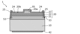
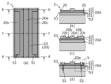
- FIG. 1 is a top view of a semiconductor laser device according to an embodiment.
- 2A is a cross-sectional view of the semiconductor laser device according to the embodiment taken along line IIA-IIA of FIG. 1.
- FIG. 2B is a cross-sectional view of the semiconductor laser device according to the embodiment taken along line IIB-IIB in FIG.
- FIG. 2C is a cross-sectional view of the semiconductor laser device according to the embodiment taken along line IIC-IIC in FIG.
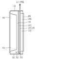
- FIG. 3 is a side view of the semiconductor laser device according to the embodiment.
- FIG. 4A is a diagram for explaining a step of forming a semiconductor laminated structure in the method of manufacturing a semiconductor laser device according to the embodiment.
- FIG. 4A is a diagram for explaining a step of forming a semiconductor laminated structure in the method of manufacturing a semiconductor laser device according to the embodiment.
- FIG. 4B is a diagram for explaining a step of forming a first resist in the method of manufacturing the semiconductor laser device according to the embodiment
- FIG. 4C is a diagram for explaining the first etching step in the method of manufacturing the semiconductor laser device according to the embodiment.
- FIG. 4D is a diagram for explaining the step of removing the first resist in the method of manufacturing the semiconductor laser device according to the embodiment.
- FIG. 4E is a diagram for explaining a step of forming a second resist in the method of manufacturing the semiconductor laser device according to the embodiment;
- FIG. 4F is a diagram for explaining the second etching step in the method of manufacturing the semiconductor laser device according to the embodiment.
- FIG. 4G is a diagram for explaining a step of forming an insulating film in the method of manufacturing the semiconductor laser device according to the embodiment
- FIG. 4H is a diagram for explaining the step of removing the insulating film in the method of manufacturing the semiconductor laser device according to the embodiment.
- FIG. FIG. 4I is a diagram for explaining the step of forming the p-side electrode in the method of manufacturing the semiconductor laser device according to the embodiment.
- FIG. 4J is a diagram for explaining the step of forming the n-side electrode in the method of manufacturing the semiconductor laser device according to the embodiment.
- FIG. 5 is a cross-sectional SEM image of a portion corresponding to a region V surrounded by a broken line in (d) of FIG. 4H.
- FIG. 6 is a diagram showing the configuration of a semiconductor laser device manufactured by the method for manufacturing a semiconductor laser device according to the embodiment.
- FIG. 7 is a cross-sectional view of a semiconductor laser device according to a modification.
- FIG. 8 is a diagram for explaining the step of dividing the bar-shaped substrate into a plurality of semiconductor laser elements (dividing step).
- FIG. 9 is a diagram showing the configuration of a semiconductor laser device of a comparative example.
- a plurality of bar-shaped substrates are produced by dividing a semiconductor laminated substrate in which a plurality of semiconductor layers are laminated on a wafer substrate (primary division step). After coating films are formed on both end surfaces of the bar-shaped substrate, the bar-shaped substrate is further divided into a plurality of pieces, thereby separating into a plurality of semiconductor laser elements (secondary division step). This makes it possible to obtain a plurality of semiconductor laser elements to be laser chips from one wafer.
- grooves (guide grooves) for division are formed in the semiconductor laminated substrate or the bar-shaped substrate in advance, and the bar-shaped substrate is divided into a plurality of pieces along the grooves.
- the ends of the grooves in the direction of the cavity should be set back from the cavity facets. is irradiated with a laser beam.
- the laser light is irradiated so that the dividing grooves do not reach the positions of the resonator facets on the front side and the rear side of the bar-shaped substrate.
- a bar-shaped substrate 3X having dividing grooves 51X formed on the back surface of the substrate 10X is sandwiched between an adhesive sheet 101 and a protective film 102, and bar-shaped substrates are placed at positions corresponding to the dividing grooves 51X.
- a blade-like jig 103 such as a cutter is pushed in sequentially from above the substrate 3X.
- FIG. 9 is a diagram showing the configuration of a semiconductor laser device 1X of a comparative example when manufactured by the method of Patent Document 1.
- FIG. 9 (a) is a top view of the semiconductor laser element 1X, (b) is a cross-sectional view taken along line bb in (a), and (c) is cc in (a).
- 1 is a cross-sectional view on line;
- FIG. 9(d) is a side view of the semiconductor laser element 1X viewed from the rear facet side, with the coating film 32X on the facet being omitted.
- the thick line in FIG. 9 indicates the crack 90X generated in the semiconductor laser element 1X, and the hatched area of dots in FIG. 9A indicates the area where the crack 90X is generated.
- the cracks 90X spread in a triangular plane, as shown in FIG. 9(a). Specifically, as shown in (b) and (d) of FIG. 9, many cracks 90X that occur are formed on the side surface of the semiconductor lamination structure 20X in the cross section perpendicular to the cavity length direction of the semiconductor laser element 1X. First, the crack progresses obliquely upward in the vicinity of the groove 51X, and then extends obliquely upward at an angle of about 1.5° with respect to the main surface of the substrate 10X at a location away from the groove 51X.
- the film thickness of the coating film 32X formed on the rear side of the cavity facet is thicker than the thickness of the coating film 31X formed on the front side of the cavity facet in order to emit the laser light in the front direction. (for example, about eight times), the vicinities of the resonator facets on the rear side are less likely to crack than the resonator facets on the front side. Therefore, it is considered that many cracks 90X were generated on the rear-side resonator facet.
- the present disclosure has been made to solve the problem of crack generation, and is a semiconductor laser that can suppress the progress of cracks below the ridge portion even if cracks are generated during separation into individual pieces.
- a first object is to obtain a device.
- a protective member such as SiO 2 may be placed on the wafer.
- the ridge may be chipped (such as a step on the end surface) due to the stress applied during division.
- a second object of the present disclosure is to obtain a semiconductor laser device capable of suppressing the occurrence of cracks in the ridge portion during the division process. .
- each figure is a schematic diagram and is not necessarily strictly illustrated. Therefore, the scales and the like are not always the same in each drawing. In each figure, the same reference numerals are assigned to substantially the same configurations, and duplicate descriptions are omitted or simplified.
- the terms “upper” and “lower” do not refer to the upward direction (vertically upward) and the downward direction (vertically downward) in absolute spatial recognition, but are based on the stacking order in the stacking structure. It is used as a term defined by a relative positional relationship. Also, the terms “above” and “below” are used not only when two components are spaced apart from each other and there is another component between the two components, but also when two components are spaced apart from each other. It also applies when they are arranged in contact with each other.
- FIG. 1 is a top view of a semiconductor laser device 1 according to an embodiment.
- 2A to 2C are cross-sectional views of the semiconductor laser device 1 according to the embodiment.
- 2A is a cross-sectional view along line IIA-IIA in FIG. 1
- FIG. 2B is a cross-sectional view along line IIB-IIB in FIG. 1
- FIG. 2C is a cross-sectional view along line IIC-IIC in FIG.
- FIG. 3 is a side view of the semiconductor laser device 1 according to the embodiment. Note that the insulating film 81 is omitted in FIG.
- a semiconductor laser device 1 has a front facet 1a and a rear facet 1b, which are cavity facets, and a first side face 1c and a second side face 1d, which are faces intersecting the cavity facets.
- the front facet 1a is a facet on the front side of the semiconductor laser element 1, and is a cavity facet from which laser light is emitted.
- the rear facet 1b is a facet on the rear side of the semiconductor laser element 1, and is a cavity facet from which laser light is not emitted.
- the front facet 1a and the rear facet 1b face each other as a pair of resonator facets.
- the rear end face 1b is the end face opposite to the front end face 1a.
- the first side face 1c is one side face of the semiconductor laser element 1.
- the second side surface 1 d is the other side surface of the semiconductor laser element 1 .
- the first side surface 1c and the second side surface 1d face each other as a pair of side surfaces.
- the first side surface 1c and the second side surface 1d are surfaces orthogonal to the front end surface 1a and the rear end surface 1b.
- the semiconductor laser device 1 has a substrate 10 and a semiconductor lamination structure 20 formed on one surface of the substrate 10 .
- the semiconductor laminated structure 20 is a structure in which a plurality of semiconductor layers are laminated, and has a PN junction.
- the semiconductor laser element 1 in this embodiment is a nitride semiconductor laser made of a nitride-based semiconductor material. Therefore, the semiconductor laminated structure 20 is a nitride semiconductor laminated body in which a plurality of nitride semiconductor layers each made of a nitride semiconductor material are laminated. Specifically, the semiconductor laser device 1 is a GaN-based nitride semiconductor laser. Laser light emitted from the semiconductor laser element 1 is, for example, light in a wavelength band from ultraviolet to blue.
- the semiconductor laser device 1 has an optical waveguide with a front facet 1a and a rear facet 1b as resonator reflection mirrors.
- the semiconductor laminated structure 20 has an optical waveguide.
- the optical waveguide extends along the resonator length direction of the semiconductor laser device 1 .
- the semiconductor laminated structure 20 is formed with a ridge portion 20a as an optical waveguide. Therefore, the ridge portion 20a is formed so as to extend along the cavity length direction of the semiconductor laser device 1 .
- the ridge portion 20 a has a convex shape and is formed by digging the semiconductor laminated structure 20 .
- the semiconductor laser element 1 has a shape elongated in the cavity length direction.
- the length of the semiconductor laser device 1 in the cavity length direction is, for example, 800 ⁇ m or more, and is 1200 ⁇ m in this embodiment.
- a laser resonator is formed by the front facet 1a and the rear facet 1b. Therefore, the rear facet 1b has a higher reflectance than the front facet 1a. As an example, the reflectance of the front facet 1a is 5%, and the reflectance of the rear facet 1b is 95%.
- a first coating film 31 is formed as a reflective film on the front side of the semiconductor laser device 1, and a second coating film 31 is formed on the rear side of the semiconductor laser device 1 as a reflective film.
- a two-coat film 32 is formed.
- the first coat film 31 is formed on the front end face of the semiconductor laminated structure 20
- the second coat film 32 is formed on the rear end face of the semiconductor laminated structure 20 .
- the first coat film 31 and the second coat film 32 are composed of a dielectric multilayer film in which a plurality of dielectric films are laminated.
- the film thickness of the second coat film 32 on the rear side is larger than the film thickness of the first coat film 31 on the front side.
- the film thickness of the second coat film 32 is at least twice as large as the film thickness of the first coat film 31, and is approximately eight times as large in the present embodiment.
- the substrate 10 is a semiconductor substrate made of GaN, SiC, or the like, or an insulating substrate such as a sapphire substrate.
- the substrate 10 is, for example, an n-type GaN substrate made of hexagonal GaN single crystal.
- an n-type GaN substrate having a (0001) plane as the main surface is used as the substrate 10.
- the semiconductor laminated structure 20 has an n-side first semiconductor layer 21, an active layer 22, and a p-side second semiconductor layer 23 on the substrate 10 in this order.
- the active layer 22 is a PN junction in the semiconductor laminated structure 20 .
- the first semiconductor layer 21, the active layer 22, and the second semiconductor layer 23 are formed by epitaxially growing a nitride-based semiconductor material using a metal organic chemical vapor deposition (MOCVD) method. can be done.
- MOCVD metal organic chemical vapor deposition
- the first semiconductor layer 21 includes at least an n-type clad layer.
- the first semiconductor layer 21 has an n-side clad layer including an n-type clad layer and an n-side optical guide layer formed on the n-side clad layer.
- the n-side cladding layer and the n-side optical guide layer may be either a single layer or multiple layers.
- the n-side clad layer is an n-side clad layer (n-AlGaN layer) made of AlGaN doped with silicon.
- the n-side optical guide layer is an optical guide layer (un-GaN layer) made of undoped GaN.
- the active layer 22 is a quantum well active layer.
- the active layer 22 has a laminated structure in which well layers (well layers) made of undoped InGaN and barrier layers (barrier layers) made of undoped InGaN are alternately laminated.
- the active layer 22 may have either a single quantum well structure (SQW) or a multiple quantum well structure (MQW).
- the active layer 22 has a five-layer structure including a barrier layer made of InGaN, a well layer made of InGaN, a barrier layer made of InGaN, a well layer made of InGaN, and a barrier layer made of InGaN. be.
- the second semiconductor layer 23 includes at least a p-type clad layer.
- the second semiconductor layer 23 includes a p-side optical guide layer, an OFS layer (overflow suppression layer) formed on the p-side optical guide layer, and an OFS layer formed on the p-type optical guide layer. It has a p-side clad layer including a clad layer and a contact layer formed on the p-side clad layer.
- the p-side optical guide layer, OFS layer, p-side cladding layer and contact layer may be either a single layer or multiple layers.
- the p-side optical guide layer is a p-side optical guide layer (un-GaN layer) made of undoped GaN.
- the OFS layer is a p-type OFS layer (p-AlGaN layer) made of AlGaN doped with magnesium as an impurity.
- the p-side clad layer is a p-type p-side clad layer (p-AlGaN layer) doped with magnesium as an impurity.
- the contact layer is a p-type contact layer (p-GaN layer) made of GaN doped with magnesium as an impurity.
- a concave portion 24 is formed in the semiconductor laminated structure 20 configured as described above, as shown in FIGS. 1 to 2C.
- the semiconductor laminated structure 20 is formed with a ridge portion 20a and a flat portion 20b extending laterally from the base of the ridge portion 20a.
- the recess 24 is formed by digging the semiconductor laminated structure 20 by etching. As shown in FIGS. 2A to 2C, in the present embodiment, the recess 24 digs into the second semiconductor layer 23 . That is, the ridge portion 20 a and the flat portion 20 b are formed in the second semiconductor layer 23 .
- the ridge portion 20a is formed in the p-side clad layer and the contact layer.
- the ridge portion 20a is composed of a convex portion formed on the p-side clad layer and a contact layer formed on the convex portion, and the uppermost layer of the ridge portion 20a is the contact layer.
- the flat portion 20b is formed in the p-side clad layer. The flat surface of the flat portion 20 b is the bottom of the recess 24 and the surface of the p-side clad layer in the recess 24 .
- the width and height of the ridge portion 20a are not particularly limited, but as an example, the ridge width (stripe width) of the ridge portion 20a is 1 ⁇ m or more and 100 ⁇ m or less, and the height of the ridge portion 20a is 100 nm or more and 1000 nm. It is below. Although the width of the contact layer is the same as the ridge width of the ridge portion 20a, it is not limited to this.
- the semiconductor laminated structure 20 is further formed with convex wings 20c. ing. That is, the semiconductor laminated structure 20 has the ridge portion 20a and the wing portions 20c as the convex structure.
- recess 24 is formed by digging second semiconductor layer 23 . Therefore, the wing portion 20c is composed of the second semiconductor layer 23 and has the same height as the ridge portion. Specifically, the wing portion 20c is composed of a p-side clad layer and a contact layer, like the ridge portion 20a. The top surfaces of the ridge portion 20a and the wing portions 20c are both flat.
- the wing portions 20c are formed on both sides of the ridge portion 20a. That is, the semiconductor laminated structure 20 has a pair of wing portions 20c. The ridge portion 20a is sandwiched between the pair of wing portions 20c with the recess 24 interposed therebetween. The pair of wing portions 20c extends along the cavity length direction of the semiconductor laser device 1, similarly to the ridge portion 20a. Thus, by providing the wing portions 20c on both sides of the ridge portion 20a, it is possible to reduce the pressure applied to the ridge portion 20a when the semiconductor laser device 1 is junction-down mounted.
- the width of each of the pair of wing portions 20c is larger than the width of the ridge portion 20a, but the width is not limited to this. Also, the widths of the pair of wing portions 20c are the same as each other, but may be different.
- wingless portions 20d in which the wing portions 20c are not formed are formed in the vicinity of the end faces of the semiconductor laminated structure 20. As shown in FIG. That is, the wingless portion 20d is part of the recess 24. As shown in FIG. In the present embodiment, the wingless portion 20d is formed in the vicinity of each of the front end surface and the rear end surface of the semiconductor laminated structure 20. As shown in FIG.
- projections 25 are formed on the surface of the edge of the semiconductor laminated structure 20 in the wingless portion 20d in the direction orthogonal to the resonator length direction.
- the protrusion 25 is formed at the boundary between the surface of the semiconductor laminated structure 20 and the side surface of the second groove 52, which will be described later.
- the edge of the semiconductor laminated structure 20 where the protrusion 25 is formed becomes the boundary between the surface of the semiconductor laminated structure 20 and the side surface of the second groove 52 .
- the protrusion 25 is also formed at the boundary between the surface of the semiconductor laminated structure 20 and the side surface of the third groove 53, which will be described later.
- the edge of the semiconductor laminated structure 20 where the protrusion 25 is formed becomes the boundary between the surface of the semiconductor laminated structure 20 and the side surface of the third groove 53 .
- the protrusion 25 is formed in a horn shape with a triangular cross section.
- a p-side electrode 41 is formed on the ridge portion 20a of the second semiconductor layer 23, as shown in FIG. 2B. Specifically, the p-side electrode 41 is formed on the contact layer. In this embodiment, the p-side electrode 41 is formed only on the upper surface of the ridge portion 20a. The width of the p-side electrode 41 is narrower than the width of the ridge portion 20a, but may be the same as the width of the ridge portion 20a.
- the p-side electrode 41 is formed using at least one metal material such as Pt, Ti, Cr, Ni, Mo and Au, for example.
- the p-side electrode 41 may be either a single layer or multiple layers.
- the p-side electrode 41 is an electrode having a two-layer structure of a Pd layer made of Pd and having a thickness of 40 nm and a Pt layer made of Pt and having a thickness of 35 nm.
- a pad electrode may be formed on the p-side electrode 41 .
- an n-side electrode 42 is formed on the lower surface (rear surface), which is the other surface of the substrate 10 .
- the n-side electrode 42 is an ohmic electrode that makes ohmic contact with the substrate 10, which is a semiconductor substrate.
- the n-side electrode 42 is made of, for example, at least one metal material such as Cr, Ti, Ni, Pd, Pt, Au, and Ge. Also, the n-side electrode 42 may be either a single layer or multiple layers.
- the semiconductor laminated structure 20 is covered with an insulating film 81 made of a dielectric film such as SiO 2 or SiN, except for the p-side electrode 41 on the ridge portion 20a.
- the insulating film 81 is formed to cover the second semiconductor layer 23 except for the upper surface of the ridge portion 20a. That is, the insulating film 81 is formed so as to have an opening on the ridge portion 20a of the contact layer.
- the insulating film 81 functions as a current blocking film. Therefore, the opening of the insulating film 81 serves as a current injection window through which current passes. Note that the insulating film 81 may be formed up to the side surface of the semiconductor laminated structure 20 .
- a pad electrode 82 is formed on the p-side electrode 41 .
- the pad electrode 82 is in contact with the p-side electrode 41 .
- the pad electrode 82 is wider than the ridge portion 20a and is formed on the wing portion 20c. That is, the pad electrode 82 is formed on the insulating film 81 so as to cover the ridge portion 20a, the flat portion 20b (recess 24) and the wing portion 20c.
- the pad electrode 82 is made of a metal material such as Au.
- the pad electrode 82 may be formed via an adhesion auxiliary layer such as Ti. In this case, the adhesion auxiliary layer may also be part of the pad electrode 82 .
- a plurality of grooves are formed in the semiconductor laser element 1 configured as described above. Specifically, as shown in FIGS. 1 to 3, the semiconductor laser element 1 is formed with a first groove 51, a second groove 52 and a third groove 53 as a plurality of grooves.
- the first groove 51 is formed on the back side of the semiconductor laser element 1 . Specifically, the first groove 51 is formed on the back surface of the substrate 10 .
- the second groove 52 and the third groove 53 are formed on the front side of the semiconductor laser element 1 . Specifically, the second groove 52 and the third groove 53 are formed in the semiconductor laminated structure 20 .
- a first groove 51 formed in the back surface of the substrate 10 is a guide groove when dividing a wafer in which a plurality of semiconductor layers are laminated. Specifically, as will be described later, the first grooves 51 are used when dividing each of a plurality of bar-shaped substrates after dividing a semiconductor laminated substrate in which a plurality of semiconductor layers are laminated on a wafer. It is a guide groove.
- the first groove 51 is a scribed groove, and can be formed, for example, by irradiating the back surface of the substrate 10 with laser light.
- the stress applied to the semiconductor laser element 1 during the division into individual pieces can be reduced, so that the occurrence of cracks can be suppressed. .
- the first groove 51 is formed to extend in the direction of the cavity of the semiconductor laser device 1 . Also, the first groove 51 is formed on each of the pair of side surfaces of the semiconductor laser element 1 . That is, a pair of first grooves 51 are formed in the semiconductor laser element 1 . As shown in FIG. 2B, each of the pair of first grooves 51 is formed by cutting the side surface of the semiconductor laser element 1 from the back surface of the substrate 10 . A pair of first grooves 51 are formed in the side surfaces of the substrate 10 . Specifically, one of the pair of first grooves 51 extends along the resonator length direction so as to cut one side surface of the substrate 10 corresponding to the first side surface 1c. The other of the pair of first grooves 51 extends along the resonator length direction so as to cut out the other side of the substrate 10 corresponding to the second side 1d.
- both ends of each of the pair of first grooves 51 in the cavity length direction are located at positions recessed from the end faces of the semiconductor laminated structure 20 . That is, each first groove 51 is formed so that both end portions in the resonator length direction do not reach the end face of the semiconductor laminated structure 20 . Specifically, in the vicinity of the front end of the semiconductor laminated structure 20, the first groove 51 is located between the rear end of the first groove 51 in the cavity length direction and the rear end face of the semiconductor laminated structure 20. There is a portion (remaining white space) in which the semiconductor laminated structure 20 is left without forming the .
- the first groove 51 is provided between the front end of the first groove 51 in the cavity length direction and the front end surface of the semiconductor laminated structure 20 . There is a portion (remaining white space) where the semiconductor laminated structure 20 is left without being formed.
- the bottom of the first groove 51 is positioned inside the substrate 10 . That is, the first groove 51 is formed so as not to reach the semiconductor laminated structure 20 on the upper surface side of the substrate 10 from the lower surface (back surface) of the substrate 10 .
- the thickness of the substrate 10 is 83 ⁇ m
- the depth of the first groove is 55 ⁇ m
- the remaining margin is 13 ⁇ m.
- the second grooves 52 formed in the semiconductor laminated structure 20 are crack prevention grooves for preventing cracks from progressing when dividing the bar-shaped substrate into individual pieces.
- the second groove 52 can be formed by etching the semiconductor laminated structure 20 .
- the second groove 52 is formed along the cavity direction of the semiconductor laser element 1 from the end surface of the semiconductor laminated structure 20 .
- second groove 52 is formed from the rear end surface of semiconductor laminated structure 20 toward the front end surface.
- the second groove 52 is formed only in the vicinity of the rear end surface of the semiconductor laminated structure 20 .
- the second groove 52 is formed in the wingless portion 20d of the semiconductor laminated structure 20, but may be formed across the wing portion 20c.
- the second groove 52 may also be formed near the front end surface of the semiconductor laminated structure 20 .
- the second grooves 52 are formed on both sides of the ridge portion 20a, which is the optical waveguide, when viewed from above.
- a pair of second grooves 52 are formed in the semiconductor laser element 1 .
- Each of the pair of second grooves 52 is formed between the first groove 51 and the ridge portion 20a.
- one of the pair of second grooves 52 is formed between one of the pair of first grooves 51 and the ridge portion 20a in the direction orthogonal to the resonator length direction of the semiconductor laser element 1.
- the other of the pair of second grooves 52 is formed between the other of the pair of first grooves 51 and the ridge portion 20a in the direction orthogonal to the resonator length direction of the semiconductor laser element 1. As shown in FIG.
- the length of the second groove 52 in the cavity length direction is preferably 1/2 or more of the distance (remaining space) between the first groove 51 and the rear end surface of the semiconductor laminated structure 20 .
- the length of the second groove 52 in the resonator length direction is 10 ⁇ m or more from the rear end surface of the semiconductor laminated structure 20 and is 25 ⁇ m or more, which is the distance between the third groove 53 and the second groove 52 . less than double.
- the length of the second groove 52 in the cavity length direction is 14 ⁇ m for the semiconductor laser device 1 whose length in the cavity length direction is 1200 ⁇ m.
- the lengths of the pair of second grooves 52 in the resonator direction are the same, but may be different.
- the width of the second groove 52 is, for example, 10 ⁇ m or less. In the present embodiment, the width of each second groove 52 is 8 ⁇ m, but it may be narrower as long as it can be etched. The widths of the pair of second grooves 52 are the same, but may be different.
- the depth of the second groove 52 is deeper than the portion of the surface of the semiconductor laminated structure 20 that is closest to the substrate 10 .
- the portion of the surface of semiconductor laminated structure 20 closest to substrate 10 is the bottom of third groove 53 . That is, as shown in FIG. 2C, the depth of each second groove 52 is deeper than the depth of the third groove 53 .
- the bottom of the second groove 52 is positioned about 2 ⁇ m below the portion of the surface of the semiconductor laminated structure 20 that is closest to the substrate 10 .
- the depth of the second groove 52 may be equal to the depth of the third groove 53 .
- the depths of the pair of second grooves 52 are the same as each other, they may be different.
- the side surface (inner surface) of the second groove 52 is inclined. Specifically, each of the pair of opposed side surfaces of the second groove 52 is inclined. In the present embodiment, the second groove 52 is tapered so that the width of the groove gradually narrows along the depth direction.
- the third groove 53 formed in the semiconductor laminated structure 20 serves to separate the laminated semiconductor layers for each optical waveguide in a semiconductor laminated substrate in which a plurality of semiconductor layers are laminated on a wafer by epitaxial growth. It is an isolation trench (element isolation trench). Therefore, as shown in FIGS. 2A to 2C, the third grooves 53 are formed on each of the pair of side surfaces of the semiconductor laser element 1. As shown in FIGS. In other words, a pair of third grooves 53 are formed in the semiconductor laser element 1 .
- the third groove 53 can be formed by etching a plurality of laminated semiconductor layers.
- Each of the pair of third grooves 53 is formed so as to cut the side surface of the semiconductor laminated structure 20 from the upper surface of the semiconductor laminated structure 20 . Further, as shown in FIG. 1, the third groove 53 is formed so as to extend in the cavity direction of the semiconductor laser device 1 . Specifically, one of the pair of third grooves 53 extends along the resonator length direction so as to cut one side surface of the semiconductor laminated structure 20 . The other of the pair of third grooves 53 extends along the resonator length direction so as to cut out the other side surface of the semiconductor laminated structure 20 . In the present embodiment, the pair of third grooves 53 are both formed from the front end face to the rear end face of the semiconductor laminated structure 20 .
- the third groove 53 can be formed by digging from the upper surface of the semiconductor laminated structure 20 in the lamination direction. As shown in FIGS. 2A to 2C, the depth of the third groove 53 is deeper than the position of the active layer 22 which is the PN junction in the semiconductor laminated structure 20. As shown in FIGS. Moreover, in the present embodiment, the side surface of the third groove 53 is inclined. Specifically, the side surface of the third groove 53 is slanted so that the skirt widens along the depth direction.
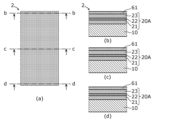
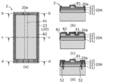
- FIGS. 4A to 4J are diagrams for explaining each step in the method of manufacturing the semiconductor laser device 1 according to the embodiment.
- (a) is a top view of the semiconductor laser device 1
- (b) is a cross-sectional view taken along line bb in (a)
- (c) is a cross-sectional view of (a). It is a cross-sectional view taken along line cc
- (d) is a cross-sectional view taken along line dd of (a).
- 4A to 4J hatching is applied for the sake of convenience in order to make it easier to understand the correspondence of the members seen on the top surface.
- the insulating film 81 is omitted.
- 4A to 4J only show a portion corresponding to one semiconductor laser element 1 of the semiconductor laminated structure 20A formed on the substrate 10, which is a wafer.
- a semiconductor laminated substrate 2 having a semiconductor laminated structure 20A is fabricated by laminating a plurality of semiconductor layers on one surface of a substrate 10, which is a wafer. Specifically, the first semiconductor layer 21, the active layer 22 and the second semiconductor layer 23 are sequentially epitaxially grown on the upper surface of the substrate 10 by the MOCVD method to form the semiconductor laminated structure 20A. After that, an insulating film 61 (first insulating film) is formed on the semiconductor laminated structure 20A. In this embodiment, an SiO 2 film is formed as the insulating film 61 . As an example, the film thickness of the insulating film 61 is 300 nm. Note that the insulating film 61 may not be formed.
- a first resist 71 having a predetermined shape and having a first opening 71a and a second opening 71b is formed above the semiconductor laminated structure 20A.
- the first opening 71a is formed at a position where a second groove 52, which will be described later, is formed.
- the second opening 71b is formed at a position where a third groove 53, which will be described later, is formed.
- the insulating film 61 is formed on the semiconductor laminated structure 20A. Formed on top.
- the semiconductor laminated structure 20A is etched (first etching step). Specifically, the semiconductor laminated structure 20A is etched using the first resist 71 having the first opening 71a and the second opening 71b as a mask. As a result, the recess 52a can be formed in the portion corresponding to the first opening 71a in the semiconductor laminated structure 20A, and the third groove 53 can be formed in the portion corresponding to the second opening 71b in the semiconductor laminated structure 20A. can be formed. Dry etching such as reactive ion etching can be used as an etching method for the semiconductor laminated structure 20A.
- the semiconductor laminated structure 20A is etched such that the bottom of the recess 52a and the bottom of the third groove 53 both reach the middle of the first semiconductor layer 21.
- the recess 52 a and the third groove 53 are formed to penetrate the second semiconductor layer 23 and the active layer 22 and reach the inside of the first semiconductor layer 21 .
- the insulating film 61 is also etched. That is, the recess 52 a and the third groove 53 also penetrate the insulating film 61 .
- the first resist 71 used as a mask is removed. Thereby, the insulating film 61 is exposed.
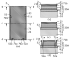
- a second resist 72 having a predetermined shape and having an opening 72a is formed above the semiconductor laminated structure 20A.
- the opening 72a is formed at a position where the recess 24 to be formed in the semiconductor laminated structure 20A is to be formed.
- openings 72 a of the second resist 72 are also formed at positions corresponding to the second grooves 52 . That is, the opening 72a is formed so as to overlap with the recess 52a formed in the semiconductor laminated structure 20A, and the recess 52a is not covered with the second resist 72.
- the third grooves 53 formed in the semiconductor laminated structure 20A are covered with the second resist 72 .
- the third groove 53 is filled with the second resist 72 .
- the second resist 72 having the opening 72a is formed on the insulating film 61. As shown in FIG.
- the semiconductor laminated structure 20A in which the recess 52a is formed is etched (second etching step). Specifically, the semiconductor laminated structure 20A is etched using the second resist 72 having the opening 72a as a mask. As a result, recesses 24 are formed in the semiconductor lamination structure 20A at portions corresponding to the openings 72a, and the ridge portion 20a and the wing portions 20c are formed in the semiconductor lamination structure 20A. Dry etching such as reactive ion etching can be used as an etching method for the semiconductor laminated structure 20A.
- the semiconductor laminated structure 20A is etched so that the bottom of the concave portion 24 reaches halfway through the second semiconductor layer 23 . That is, the ridge portion 20 a and the wing portions 20 c are formed in the second semiconductor layer 23 .
- the insulating film 61 is formed on the semiconductor laminated structure 20A, the insulating film 61 is also etched. As a result, the insulating film 61 remains only on the ridge portion 20a.
- the recesses 52a formed in the semiconductor laminated structure 20A by the first etching process are not covered with the second resist 72, the recesses 52a are further etched in this etching process. As a result, the bottom of the concave portion 52a is further deepened to form the second groove 52.
- the concave portion 52a formed up to the first semiconductor layer 21 is further etched to dig into the inside of the substrate 10 .
- the second groove 52 is formed using the first etching process for forming the third groove 53 and the second etching process for forming the ridge portion 20a. Therefore, the second grooves 52 can be formed without adding a process only for forming the second grooves 52 . That is, according to the manufacturing method of the present embodiment, it is not necessary to use a mask only for forming the second grooves 52 .
- the second resist 72 used as a mask is removed.
- the insulating film 61 on the ridge portion 20a is exposed, and the second semiconductor layer 23 in which the concave portion 24 is formed is exposed.
- the dry etching of the insulating film 61 which is the first step in forming the ridge portion 20a
- the upper side walls of the second groove 52 and the third groove 53 of the semiconductor laminated structure 20A in the wingless portion 20d are covered with the dry etching process.
- Deposits are formed by accumulating debris. Since this deposit has a slower etching rate than the insulating film 61 (the SiO 2 film in this embodiment), a small amount of the deposit remains on the sidewalls of the second groove 52 and the third groove 53 even after etching. become.
- the residual ions remain on the upper side walls of the second groove 52 and the third groove 53.
- the deposited deposits serve as a mask to form the protrusions 25 . Note that the deposits remaining on the upper side walls of the second groove 52 and the third groove 53 in the first stage are etched by the dry etching of the semiconductor laminated structure 20A and the substrate 10, so during the dry etching in the next stage. will disappear in
- an insulating film 62 (second insulating film) is formed to cover the insulating film 61 on the ridge portion 20a.
- the insulating film 62 is formed so as to cover the entire upper surface of the semiconductor laminated structure 20A.
- an SiO 2 film is formed as the insulating film 62 .
- the film thickness of the insulating film 62 is 200 nm.
- Annealing is then performed to activate the dopant in the p-type semiconductor layer.
- the ridge portion 20a is protected by the two insulating films. As a result, it is possible to prevent the ridge portion 20a from being damaged by the heat of the annealing process.
- the insulating film 62 and the insulating film 61 are removed. As a result, the entire surface of the semiconductor laminated structure 20A having the ridge portion 20a and the wing portions 20c is exposed. Therefore, the second groove 52 and the third groove 53 formed in the semiconductor laminated structure 20A are also exposed.
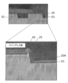
- FIG. 5 shows a cross-sectional SEM image of a portion corresponding to a region V surrounded by a broken line in (d) of FIG. 4H.
- the depth of the second groove 52 is deeper than the depth of the third groove 53 in FIG. 4H, the depth of the second groove 52 and the depth of the third groove 53 are the same in FIG.
- the semiconductor laser device 1 is shown when it is manufactured.
- the p-side electrode 41 is formed on the ridge portion 20a. Specifically, an insulating film 81 having an opening is formed on the upper surface of the ridge portion 20a, and the p-side electrode 41 is formed so as to cover the upper surface of the ridge portion 20a.
- the p-side electrode 41 can be formed into a predetermined shape using, for example, a vapor deposition method and a lift-off method. After that, a pad electrode 82 is further formed so as to straddle the p-side electrode 41 and the insulating film 81 .
- the n-side electrode 42 is formed on the back surface of the substrate 10. Then, as shown in FIG. 4J, the n-side electrode 42 is formed on the back surface of the substrate 10. Then, as shown in FIG. 4J, the n-side electrode 42 can be formed into a predetermined shape using, for example, a vapor deposition method and a lift-off method.
- the semiconductor laminated substrate 2 is divided to produce a plurality of bar-shaped substrates each having a plurality of optical waveguides (primary division step).
- a plurality of bar-shaped substrates are manufactured by cleaving and dividing the semiconductor laminated substrate 2 .
- a first groove 51 is formed in the rear surface of the semiconductor laminated substrate 2 or the bar-shaped substrate.
- the first grooves 51 are guide grooves for dividing the bar-shaped substrate into a plurality of semiconductor laser elements 1 . Therefore, the first groove 51 is formed at each boundary between two adjacent semiconductor laser elements 1 . That is, the first groove 51 is formed parallel to the longitudinal direction of the ridge portion 20a. Further, the first grooves 51 are located at positions recessed from both end faces when the semiconductor laminated substrate 2 is divided into a plurality of bar-shaped substrates. In other words, the first grooves 51 are formed so as not to reach the positions corresponding to the end faces of the plurality of bar-shaped substrates. Such first grooves 51 can be formed by irradiating the rear surface of the substrate 10 with laser light. Specifically, the first groove 51 is a laser scribed groove formed by a laser scribing method.
- the semiconductor laminated substrate 2 is divided to produce a plurality of bar-shaped substrates
- the first coat film 31 and the second coat film 32 are formed on the end surfaces of the bar-shaped substrates, and then the bars are formed along the first grooves 51 .
- a plurality of semiconductor laser devices 1 each having one optical waveguide (ridge portion 20a) are produced (secondary division step).
- the bar-shaped substrate is divided into a plurality of pieces in the same manner as the method shown in FIG. Thereby, the semiconductor laser device 1 shown in FIGS. 1 to 3 can be obtained. Some of them include those with cracks as shown in FIG.
- FIG. 6 (a) is a top view, (b) is a cross-sectional view taken along line bb in (a), and (c) is a cross-sectional view taken along line cc in (a). , (d) is a cross-sectional view taken along line dd of (a), and (e) is a side view of the semiconductor laser device 1 viewed from the rear side with the second coating film 32 omitted.
- a thick line in FIG. 6 indicates a crack 90 generated in the semiconductor laser device 1. As shown in FIG. Since the surface of the crack 90 is inclined, the depth position of the crack 90 on the side surface of the semiconductor laminated structure 20 is deeper than the depth position of the crack 90 on the dd line cross section. Also, the hatched area of dots in FIG. 6(a) indicates the area where the crack 90 occurs.
- the second groove 52 is formed in the semiconductor laminated structure 20 in the semiconductor laser device 1 manufactured as described above.
- the second groove 52 is formed along the resonator length direction from the end face of the semiconductor laminated structure 20 .
- the third groove 53 is formed in the semiconductor laminated structure 20 .
- the third groove 53 extends along the cavity length direction of the semiconductor laser element 1 so as to cut the side surface of the semiconductor laminated structure 20 .
- the depth of the second groove 52 is deeper than the portion of the surface of the semiconductor laminated structure 20 that is closest to the substrate 10 side. Specifically, as shown in (d) and (e) of FIG. 6 , the depth of the second groove 52 is deeper than the depth of the third groove 53 .
- the depth of the second groove 52A and the depth of the third groove 53 are the same, and the crack 90 is generated at a deeper position.
- the average traveling direction of the crack 90 does not intersect with the second groove 52A. change the angle of progression of the crack 90, and as a result, the progression of the crack 90 to the ridge portion 20a may be prevented. Therefore, by making the depth of the second groove 52 greater than or equal to the depth of the third groove 53 , the second groove 52 can effectively prevent the crack 90 from progressing.
- the cracks 90 are often generated from a portion approximately 2 ⁇ m below the portion of the surface of the semiconductor laminated structure 20 closest to the substrate 10 (for example, the upper surface of the third groove 53).
- the depth is preferably 2 ⁇ m or more from the portion of the surface of the semiconductor laminated structure 20 closest to the substrate 10 .
- cracks 90 generated in the cross section perpendicular to the cavity length direction of the semiconductor laser device 1 are formed in the substrate 10 from the side surface of the semiconductor laminated structure 20. It extends obliquely upward at an angle of 1.5° with respect to the main surface.
- the depth of the third groove 53 from the upper surface of the semiconductor laminated structure 20 is A
- the length from the bottom of the third groove 53 to the position of the starting point of the crack 90 in the depth direction is B
- the width of the third groove 53 on the upper surface of the semiconductor laminated structure 20 is C
- the distance from the wall surface of the third groove 53 to the inner surface outside the second groove 52 is D
- the depth of the second groove 52 is 1 ⁇ m, 3 ⁇ m
- the distance between the third groove 53 and the second groove 52 is 9 ⁇ m or less (4 ⁇ m, 7 ⁇ m, 8 ⁇ m, 9 ⁇ m)
- the width of the third groove 53 is is 4 ⁇ m.
- the length Y of the second groove 52 in the cavity length direction from the rear end surface of the semiconductor laminated structure 20 is preferably 25 times or less the distance between the third groove 53 and the second groove 52 . Thereby, it is possible to suppress the occurrence of defects such as chipping in the portion between the third groove 53 and the second groove 52 .
- the depth of the third groove 53 is the same as the depth of the active layer, which is the PN junction of the semiconductor laminated structure 20. It is deeper than the position of 22.
- the semiconductor laser element 1 can be easily separated by the third groove 53 . Further, if the depth of the third groove 53 is shallower than the position of the PN junction, the PN junction may be exposed at the time of individual separation, and leakage may occur at the PN junction. By making the height deeper than the position of the PN junction, it is possible to suppress the occurrence of leakage at the PN junction during separation into individual pieces.
- the depth of the third groove 53 By making the depth of the third groove 53 shallow, the position of the origin of the crack 90 at the corner of the semiconductor laminated structure 20 becomes shallow. In other words, the distance of the crack 90 extending upward from the side surface of the semiconductor laminated structure 20 is shortened.
- the depth of the third groove 53 is 1 ⁇ m to 3 ⁇ m. By reducing the depth of the starting point of the crack 90, the distance for the crack 90 to reach the surface can be shortened.
- the side surfaces of the second groove 52 are inclined.
- the side surface of the third groove 53 is also inclined.
- the angle formed by the upper surface of the semiconductor laminated structure 20 and the side surface of the second groove 52 can be made obtuse.
- the angle formed by the upper surface of the semiconductor laminated structure 20 and the side surface of the third groove 53 can be made obtuse.
- the distance between the second groove 52 and the ridge portion 20a is 4 ⁇ m or more when viewed from above.
- the crack 90 extending obliquely upward from the side surface of the semiconductor laser element 1 (semiconductor laminated structure 20) can be efficiently prevented from progressing by the second groove 52, and current constriction in the lateral direction can be prevented. can be done effectively.
- the second groove 52 can efficiently block the crack 90 progressing obliquely upward on the side farther from the side surface of the semiconductor laser element 1 (semiconductor laminated structure 20). In other words, the second groove 52 should be closer to the ridge portion 20 a than the side surface of the semiconductor laser element 1 .
- the length of the second groove 52 in the resonator length direction is 1/2 or more of the distance between the first groove 51 and the end surface of the semiconductor laminated structure 20 .
- the length of the second groove 52 in the resonator length direction is 14 ⁇ m, and the distance between the first groove 51 and the end surface of the semiconductor laminated structure 20 is 13 ⁇ m.
- the projection 25 is formed on the surface of the edge of the semiconductor laminated structure 20 in the direction orthogonal to the resonator length direction in the wingless portion 20d of the semiconductor laminated structure 20. ing. Specifically, the protrusion 25 is formed on the edge that is the boundary between the surface of the semiconductor laminated structure 20 and the side surface of the second groove 52 . A protrusion 25 is also formed on the edge, which is the boundary between the surface of the semiconductor laminated structure 20 and the side surface of the third groove 53 .
- the height of the protective member is equal to the height of the ridge portion 20a. Therefore, stress applied to the ridge portion 20a at the time of division can be suppressed. As a result, it is possible to suppress the occurrence of chipping (end surface step, etc.) in the ridge portion 20a due to the stress during division.
- the projections 25 are formed on the semiconductor laminated structure 20, the surface area of the semiconductor laminated structure 20 can be increased. As a result, the contact area between the solder and the semiconductor laser element 1 increases when the semiconductor laser element 1 is mounted on the submount by soldering, so that bonding and adhesion can be improved.
- the waveguide in the semiconductor laser device 1 is the ridge portion 20a, but it is not limited to this.
- the waveguide in the semiconductor laser device 1 may have an electrode stripe structure composed only of divided electrodes instead of a ridge stripe structure composed of the ridge portion 20a, or a current confinement structure using a current blocking layer. etc.
- the present invention is not limited to this.
- the present disclosure can also be applied when semiconductor materials other than nitride-based semiconductor materials are used.
- a semiconductor laser element according to the present disclosure is useful as a light source element for various products, including projectors, optical discs, vehicle-mounted headlamps, lighting devices, laser processing devices, and the like.
- Reference Signs List 1 1A semiconductor laser element 1a front facet 1b rear facet 1c first side face 1d second side face 2 semiconductor laminated substrate 10 substrate 20, 20A semiconductor laminated structure 20a ridge portion 20b flat portion 20c wing portion 20d wingless portion 21 first semiconductor Layer 22 Active layer 23 Second semiconductor layer 24 Recess 25 Protrusion 31 First coat film 32 Second coat film 41 P-side electrode 42 N-side electrode 51 First groove 52 Second groove 52a Recess 53 Third groove 61, 62 Insulating film 71 first resist 71a first opening 71b second opening 72 second resist 72a opening 81 insulating film 82 pad electrode 90 crack 101 adhesive sheet 102 protective film 103 blade jig
Landscapes
- Physics & Mathematics (AREA)
- Condensed Matter Physics & Semiconductors (AREA)
- General Physics & Mathematics (AREA)
- Electromagnetism (AREA)
- Optics & Photonics (AREA)
- Geometry (AREA)
- Semiconductor Lasers (AREA)
Priority Applications (2)
| Application Number | Priority Date | Filing Date | Title |
|---|---|---|---|
| CN202380018928.XA CN118613977A (zh) | 2022-01-31 | 2023-01-18 | 半导体激光元件及半导体激光元件的制造方法 |
| US18/781,540 US20240380180A1 (en) | 2022-01-31 | 2024-07-23 | Semiconductor laser element and method for manufacturing the same |
Applications Claiming Priority (2)
| Application Number | Priority Date | Filing Date | Title |
|---|---|---|---|
| JP2022012749A JP2023111096A (ja) | 2022-01-31 | 2022-01-31 | 半導体レーザ素子及び半導体レーザ素子の製造方法 |
| JP2022-012749 | 2022-01-31 |
Related Child Applications (1)
| Application Number | Title | Priority Date | Filing Date |
|---|---|---|---|
| US18/781,540 Continuation US20240380180A1 (en) | 2022-01-31 | 2024-07-23 | Semiconductor laser element and method for manufacturing the same |
Publications (1)
| Publication Number | Publication Date |
|---|---|
| WO2023145562A1 true WO2023145562A1 (ja) | 2023-08-03 |
Family
ID=87471444
Family Applications (1)
| Application Number | Title | Priority Date | Filing Date |
|---|---|---|---|
| PCT/JP2023/001298 Ceased WO2023145562A1 (ja) | 2022-01-31 | 2023-01-18 | 半導体レーザ素子及び半導体レーザ素子の製造方法 |
Country Status (4)
| Country | Link |
|---|---|
| US (1) | US20240380180A1 (https=) |
| JP (1) | JP2023111096A (https=) |
| CN (1) | CN118613977A (https=) |
| WO (1) | WO2023145562A1 (https=) |
Citations (12)
| Publication number | Priority date | Publication date | Assignee | Title |
|---|---|---|---|---|
| JP2007180522A (ja) * | 2005-11-30 | 2007-07-12 | Sharp Corp | 窒化物系半導体レーザ素子及びその製造方法 |
| JP2008160070A (ja) * | 2006-11-30 | 2008-07-10 | Sanyo Electric Co Ltd | 窒化物系半導体素子およびその製造方法 |
| JP2008300584A (ja) * | 2007-05-31 | 2008-12-11 | Sharp Corp | 窒化物系半導体レーザ素子及びその製造方法 |
| JP2008305911A (ja) * | 2007-06-06 | 2008-12-18 | Sharp Corp | 窒化物系半導体レーザ素子及びその製造方法 |
| JP2009004524A (ja) * | 2007-06-21 | 2009-01-08 | Sanyo Electric Co Ltd | 窒化物系半導体レーザ素子及び窒化物系半導体レーザ素子の作製方法 |
| JP2010199139A (ja) * | 2009-02-23 | 2010-09-09 | Nichia Corp | 半導体レーザ素子の製造方法 |
| US20120189029A1 (en) * | 2010-12-07 | 2012-07-26 | Rohm Co., Ltd. | Semiconductor laser device |
| JP2012178508A (ja) * | 2011-02-28 | 2012-09-13 | Sanyo Electric Co Ltd | 半導体レーザ素子およびその製造方法 |
| JP2018530151A (ja) * | 2015-10-01 | 2018-10-11 | オスラム オプト セミコンダクターズ ゲゼルシャフト ミット ベシュレンクテル ハフツングOsram Opto Semiconductors GmbH | オプトエレクトロニクス部品 |
| WO2020137146A1 (ja) * | 2018-12-28 | 2020-07-02 | ローム株式会社 | 半導体レーザ素子 |
| JP2020127003A (ja) * | 2019-02-05 | 2020-08-20 | シャープ株式会社 | 半導体レーザ素子 |
| US20200321749A1 (en) * | 2016-07-15 | 2020-10-08 | Osram Opto Semiconductors Gmbh | Semiconductor laser diode |
Family Cites Families (6)
| Publication number | Priority date | Publication date | Assignee | Title |
|---|---|---|---|---|
| JP2008021885A (ja) * | 2006-07-13 | 2008-01-31 | Matsushita Electric Ind Co Ltd | 半導体ウェハ、半導体素子、半導体ウェハの製造方法、半導体素子の製造方法 |
| WO2008047751A1 (en) * | 2006-10-17 | 2008-04-24 | Sanyo Electric Co., Ltd. | Nitride semiconductor laser device and its manufacturing method |
| JP2009200478A (ja) * | 2008-01-21 | 2009-09-03 | Sanyo Electric Co Ltd | 半導体レーザ素子およびその製造方法 |
| JP2010258050A (ja) * | 2009-04-22 | 2010-11-11 | Sanyo Electric Co Ltd | 半導体レーザ素子の製造方法 |
| JP5689297B2 (ja) * | 2010-12-07 | 2015-03-25 | ローム株式会社 | 半導体レーザ素子およびその製造方法 |
| JP2012124273A (ja) * | 2010-12-07 | 2012-06-28 | Rohm Co Ltd | 半導体レーザ素子 |
-
2022
- 2022-01-31 JP JP2022012749A patent/JP2023111096A/ja active Pending
-
2023
- 2023-01-18 WO PCT/JP2023/001298 patent/WO2023145562A1/ja not_active Ceased
- 2023-01-18 CN CN202380018928.XA patent/CN118613977A/zh active Pending
-
2024
- 2024-07-23 US US18/781,540 patent/US20240380180A1/en active Pending
Patent Citations (12)
| Publication number | Priority date | Publication date | Assignee | Title |
|---|---|---|---|---|
| JP2007180522A (ja) * | 2005-11-30 | 2007-07-12 | Sharp Corp | 窒化物系半導体レーザ素子及びその製造方法 |
| JP2008160070A (ja) * | 2006-11-30 | 2008-07-10 | Sanyo Electric Co Ltd | 窒化物系半導体素子およびその製造方法 |
| JP2008300584A (ja) * | 2007-05-31 | 2008-12-11 | Sharp Corp | 窒化物系半導体レーザ素子及びその製造方法 |
| JP2008305911A (ja) * | 2007-06-06 | 2008-12-18 | Sharp Corp | 窒化物系半導体レーザ素子及びその製造方法 |
| JP2009004524A (ja) * | 2007-06-21 | 2009-01-08 | Sanyo Electric Co Ltd | 窒化物系半導体レーザ素子及び窒化物系半導体レーザ素子の作製方法 |
| JP2010199139A (ja) * | 2009-02-23 | 2010-09-09 | Nichia Corp | 半導体レーザ素子の製造方法 |
| US20120189029A1 (en) * | 2010-12-07 | 2012-07-26 | Rohm Co., Ltd. | Semiconductor laser device |
| JP2012178508A (ja) * | 2011-02-28 | 2012-09-13 | Sanyo Electric Co Ltd | 半導体レーザ素子およびその製造方法 |
| JP2018530151A (ja) * | 2015-10-01 | 2018-10-11 | オスラム オプト セミコンダクターズ ゲゼルシャフト ミット ベシュレンクテル ハフツングOsram Opto Semiconductors GmbH | オプトエレクトロニクス部品 |
| US20200321749A1 (en) * | 2016-07-15 | 2020-10-08 | Osram Opto Semiconductors Gmbh | Semiconductor laser diode |
| WO2020137146A1 (ja) * | 2018-12-28 | 2020-07-02 | ローム株式会社 | 半導体レーザ素子 |
| JP2020127003A (ja) * | 2019-02-05 | 2020-08-20 | シャープ株式会社 | 半導体レーザ素子 |
Also Published As
| Publication number | Publication date |
|---|---|
| JP2023111096A (ja) | 2023-08-10 |
| CN118613977A (zh) | 2024-09-06 |
| US20240380180A1 (en) | 2024-11-14 |
Similar Documents
| Publication | Publication Date | Title |
|---|---|---|
| CN101316026B (zh) | 氮化物半导体激光器芯片及其制造方法 | |
| CN101361238B (zh) | 半导体激光元件及其制造方法 | |
| US8686432B2 (en) | Semiconductor light emitting device with laser scribed end faces | |
| JP7146736B2 (ja) | 窒化物半導体発光素子の製造方法 | |
| JP2009081428A (ja) | 半導体発光素子およびその製造方法 | |
| JP7085549B2 (ja) | 半導体発光素子の製造方法及び半導体発光素子 | |
| JP2009200478A (ja) | 半導体レーザ素子およびその製造方法 | |
| JP2009071162A (ja) | 半導体装置及び半導体装置の製造方法 | |
| US20110013659A1 (en) | Semiconductor laser device and method of manufacturing the same | |
| JP2014183120A (ja) | 半導体装置およびその製造方法並びに半導体ウェハ | |
| CN101529674B (zh) | 氮化物类半导体激光元件及其制造方法 | |
| TW201835989A (zh) | 氮化物半導體雷射元件及其製造方法 | |
| EP3493338B1 (en) | Semiconductor light-emitting element and method for manufacturing semiconductor light-emitting element | |
| CN101262119A (zh) | 半导体激光器的制造方法 | |
| JP2005012206A (ja) | 窒化物系半導体素子およびその製造方法 | |
| TW201725660A (zh) | 發光元件及其製造方法 | |
| JP5273459B2 (ja) | 半導体レーザの製造方法 | |
| WO2023145562A1 (ja) | 半導体レーザ素子及び半導体レーザ素子の製造方法 | |
| JP5689297B2 (ja) | 半導体レーザ素子およびその製造方法 | |
| JP4613395B2 (ja) | 半導体レーザ素子及びその製造方法 | |
| JP2020088182A (ja) | 半導体レーザアレイ装置 | |
| US20170244220A1 (en) | Semiconductor light-emitting device and method for manufacturing the same | |
| WO2023219132A1 (ja) | 半導体レーザ素子及び半導体レーザ素子の製造方法 | |
| JP6985080B2 (ja) | 半導体光素子及びその製造方法 | |
| JP6520527B2 (ja) | 半導体レーザ素子の製造方法 |
Legal Events
| Date | Code | Title | Description |
|---|---|---|---|
| 121 | Ep: the epo has been informed by wipo that ep was designated in this application |
Ref document number: 23746776 Country of ref document: EP Kind code of ref document: A1 |
|
| WWE | Wipo information: entry into national phase |
Ref document number: 202380018928.X Country of ref document: CN |
|
| NENP | Non-entry into the national phase |
Ref country code: DE |
|
| 122 | Ep: pct application non-entry in european phase |
Ref document number: 23746776 Country of ref document: EP Kind code of ref document: A1 |