WO2023145562A1 - 半導体レーザ素子及び半導体レーザ素子の製造方法 - Google Patents
半導体レーザ素子及び半導体レーザ素子の製造方法 Download PDFInfo
- Publication number
- WO2023145562A1 WO2023145562A1 PCT/JP2023/001298 JP2023001298W WO2023145562A1 WO 2023145562 A1 WO2023145562 A1 WO 2023145562A1 JP 2023001298 W JP2023001298 W JP 2023001298W WO 2023145562 A1 WO2023145562 A1 WO 2023145562A1
- Authority
- WO
- WIPO (PCT)
- Prior art keywords
- semiconductor
- groove
- laminated structure
- semiconductor laser
- substrate
- Prior art date
Links
- 239000004065 semiconductor Substances 0.000 title claims abstract description 424
- 238000004519 manufacturing process Methods 0.000 title claims description 25
- 239000000758 substrate Substances 0.000 claims abstract description 124
- 230000003287 optical effect Effects 0.000 claims abstract description 40
- 238000000034 method Methods 0.000 claims description 43
- 238000005530 etching Methods 0.000 claims description 31
- 238000010030 laminating Methods 0.000 claims description 3
- 239000010410 layer Substances 0.000 description 127
- 230000008569 process Effects 0.000 description 20
- 238000010586 diagram Methods 0.000 description 16
- 150000004767 nitrides Chemical class 0.000 description 12
- 239000011248 coating agent Substances 0.000 description 7
- 238000000576 coating method Methods 0.000 description 7
- 238000001312 dry etching Methods 0.000 description 7
- 238000003475 lamination Methods 0.000 description 7
- 239000000463 material Substances 0.000 description 7
- 229910004298 SiO 2 Inorganic materials 0.000 description 6
- 230000002250 progressing effect Effects 0.000 description 6
- 229910002704 AlGaN Inorganic materials 0.000 description 5
- 230000004888 barrier function Effects 0.000 description 5
- 230000001681 protective effect Effects 0.000 description 5
- 239000000470 constituent Substances 0.000 description 4
- 230000001678 irradiating effect Effects 0.000 description 4
- 238000000926 separation method Methods 0.000 description 4
- 239000002356 single layer Substances 0.000 description 4
- FYYHWMGAXLPEAU-UHFFFAOYSA-N Magnesium Chemical compound [Mg] FYYHWMGAXLPEAU-UHFFFAOYSA-N 0.000 description 3
- 230000006866 deterioration Effects 0.000 description 3
- 239000012535 impurity Substances 0.000 description 3
- 229910052749 magnesium Inorganic materials 0.000 description 3
- 239000011777 magnesium Substances 0.000 description 3
- 239000007769 metal material Substances 0.000 description 3
- 230000004048 modification Effects 0.000 description 3
- 238000012986 modification Methods 0.000 description 3
- JMASRVWKEDWRBT-UHFFFAOYSA-N Gallium nitride Chemical compound [Ga]#N JMASRVWKEDWRBT-UHFFFAOYSA-N 0.000 description 2
- 239000000853 adhesive Substances 0.000 description 2
- 230000001070 adhesive effect Effects 0.000 description 2
- 238000000137 annealing Methods 0.000 description 2
- 230000000903 blocking effect Effects 0.000 description 2
- 229910052804 chromium Inorganic materials 0.000 description 2
- 238000005253 cladding Methods 0.000 description 2
- 230000000052 comparative effect Effects 0.000 description 2
- 239000013078 crystal Substances 0.000 description 2
- 238000005520 cutting process Methods 0.000 description 2
- 229910052737 gold Inorganic materials 0.000 description 2
- 238000002955 isolation Methods 0.000 description 2
- 229910052759 nickel Inorganic materials 0.000 description 2
- 238000001020 plasma etching Methods 0.000 description 2
- 229910052697 platinum Inorganic materials 0.000 description 2
- 238000012545 processing Methods 0.000 description 2
- 238000001878 scanning electron micrograph Methods 0.000 description 2
- 229910052719 titanium Inorganic materials 0.000 description 2
- 238000007740 vapor deposition Methods 0.000 description 2
- JBRZTFJDHDCESZ-UHFFFAOYSA-N AsGa Chemical compound [As]#[Ga] JBRZTFJDHDCESZ-UHFFFAOYSA-N 0.000 description 1
- 229910001218 Gallium arsenide Inorganic materials 0.000 description 1
- 230000008859 change Effects 0.000 description 1
- 238000005229 chemical vapour deposition Methods 0.000 description 1
- 238000003776 cleavage reaction Methods 0.000 description 1
- 230000007547 defect Effects 0.000 description 1
- 239000002019 doping agent Substances 0.000 description 1
- 229910052732 germanium Inorganic materials 0.000 description 1
- 230000012447 hatching Effects 0.000 description 1
- 238000002347 injection Methods 0.000 description 1
- 239000007924 injection Substances 0.000 description 1
- 150000002500 ions Chemical class 0.000 description 1
- 229910052751 metal Inorganic materials 0.000 description 1
- 239000002184 metal Substances 0.000 description 1
- 229910052750 molybdenum Inorganic materials 0.000 description 1
- 229910052763 palladium Inorganic materials 0.000 description 1
- 230000002093 peripheral effect Effects 0.000 description 1
- 230000002265 prevention Effects 0.000 description 1
- 238000012827 research and development Methods 0.000 description 1
- 229910052594 sapphire Inorganic materials 0.000 description 1
- 239000010980 sapphire Substances 0.000 description 1
- 230000007017 scission Effects 0.000 description 1
- 229910052710 silicon Inorganic materials 0.000 description 1
- 239000010703 silicon Substances 0.000 description 1
- 229910000679 solder Inorganic materials 0.000 description 1
- 238000005476 soldering Methods 0.000 description 1
- 230000001629 suppression Effects 0.000 description 1
Images


Classifications
-
- H—ELECTRICITY
- H01—ELECTRIC ELEMENTS
- H01S—DEVICES USING THE PROCESS OF LIGHT AMPLIFICATION BY STIMULATED EMISSION OF RADIATION [LASER] TO AMPLIFY OR GENERATE LIGHT; DEVICES USING STIMULATED EMISSION OF ELECTROMAGNETIC RADIATION IN WAVE RANGES OTHER THAN OPTICAL
- H01S5/00—Semiconductor lasers
- H01S5/20—Structure or shape of the semiconductor body to guide the optical wave ; Confining structures perpendicular to the optical axis, e.g. index or gain guiding, stripe geometry, broad area lasers, gain tailoring, transverse or lateral reflectors, special cladding structures, MQW barrier reflection layers
- H01S5/22—Structure or shape of the semiconductor body to guide the optical wave ; Confining structures perpendicular to the optical axis, e.g. index or gain guiding, stripe geometry, broad area lasers, gain tailoring, transverse or lateral reflectors, special cladding structures, MQW barrier reflection layers having a ridge or stripe structure
Definitions
- the present disclosure relates to a semiconductor laser device and a method for manufacturing a semiconductor laser device.
- semiconductor laser elements have advantages such as long life, high efficiency, and small size, they are used as light sources for various products such as projectors, optical discs, in-vehicle headlamps, lighting devices, and laser processing devices. 2. Description of the Related Art In recent years, as a semiconductor laser element, research and development of a nitride-based semiconductor laser capable of covering a wavelength band from ultraviolet to blue has been advanced.
- a semiconductor laser element is produced by cutting out a plurality of bar-shaped substrates by dividing a semiconductor laminated substrate in which a plurality of semiconductor layers are laminated on a wafer, and further dividing the bar-shaped substrates into a plurality of individual pieces.
- problems such as the division being deviated from the planned dividing line or the part being chipped occur.
- nitride semiconductor lasers are split along crystal planes instead of cleavage planes in the splitting process. It is easy to cause troubles such as being deviated and split or partly missing.
- Patent Literature 1 discloses a method of dividing a wafer by irradiating the rear surface of the wafer on which a plurality of semiconductor layers are laminated with a laser beam to form dividing grooves.
- Patent Document 1 Even if the method disclosed in Patent Document 1 is used, a dividing step of dividing a semiconductor laminated substrate in which a plurality of semiconductor layers are laminated on a wafer, or a dividing step of dividing a bar-shaped substrate obtained by dividing a semiconductor laminated substrate. There is a problem that cracks are generated in the semiconductor laser element during the process, and the reliability of the semiconductor laser element is lowered.
- the present disclosure has been made to solve such problems, and provides a semiconductor laser device and a method for manufacturing the semiconductor laser device that can suppress deterioration in reliability due to cracks that occur during the manufacturing process. for the purpose.
- a first semiconductor laser device having a cavity facet and a pair of side faces intersecting the cavity facet, comprising: a substrate; a semiconductor lamination structure formed on one surface of the substrate and having a plurality of laminated semiconductor layers, wherein the semiconductor lamination structure extends along the cavity length direction of the semiconductor laser element.
- a pair of first grooves extending along the resonator length direction are formed on the other surface of the substrate so as to cut out the pair of side surfaces. Both ends of each groove in the cavity length direction are located at positions recessed from the end face of the semiconductor laminated structure, and the semiconductor laminated structure has a groove extending from the end face of the semiconductor laminated structure in the cavity length direction. and the second grooves are formed on both sides of the optical waveguide and between the first groove and the optical waveguide when viewed from above.
- one aspect of a second semiconductor laser device includes a substrate, and a semiconductor laminated structure formed on one surface of the substrate and having a plurality of semiconductor layers laminated, wherein the semiconductor laminated structure
- the structure has a ridge portion extending in a cavity length direction of the semiconductor laser element, and wing portions formed on both sides of the ridge portion to have the same height as the ridge portion, and the semiconductor laminated structure.
- a wingless portion in which the wing portion is not formed is formed in the vicinity of the end face of the . , a protrusion is formed.
- one aspect of a method for manufacturing a semiconductor laser device includes a step of manufacturing a semiconductor laminated substrate having a semiconductor laminated structure by laminating a plurality of semiconductor layers on one surface of a substrate; a first etching step of etching the structure; a second etching step of etching the semiconductor laminated structure after the first etching step; forming a first groove in the rear surface of the semiconductor laminated substrate or the bar-shaped substrate; and dividing the bar-shaped substrate along the first groove.
- the first etching step forms a recess in the semiconductor laminated structure
- the second etching step includes A recess is further etched to form a second groove, and a ridge portion is formed in the semiconductor laminated structure as the optical waveguide, and the second groove is formed on both sides of the optical waveguide in a top view. It is formed to extend along the cavity length direction of the semiconductor laser element from the end face of the structure, and is formed between the first groove and the optical waveguide.
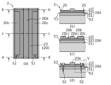
- FIG. 1 is a top view of a semiconductor laser device according to an embodiment.
- 2A is a cross-sectional view of the semiconductor laser device according to the embodiment taken along line IIA-IIA of FIG. 1.
- FIG. 2B is a cross-sectional view of the semiconductor laser device according to the embodiment taken along line IIB-IIB in FIG.
- FIG. 2C is a cross-sectional view of the semiconductor laser device according to the embodiment taken along line IIC-IIC in FIG.
- FIG. 3 is a side view of the semiconductor laser device according to the embodiment.
- FIG. 4A is a diagram for explaining a step of forming a semiconductor laminated structure in the method of manufacturing a semiconductor laser device according to the embodiment.
- FIG. 4A is a diagram for explaining a step of forming a semiconductor laminated structure in the method of manufacturing a semiconductor laser device according to the embodiment.
- FIG. 4B is a diagram for explaining a step of forming a first resist in the method of manufacturing the semiconductor laser device according to the embodiment
- FIG. 4C is a diagram for explaining the first etching step in the method of manufacturing the semiconductor laser device according to the embodiment.
- FIG. 4D is a diagram for explaining the step of removing the first resist in the method of manufacturing the semiconductor laser device according to the embodiment.
- FIG. 4E is a diagram for explaining a step of forming a second resist in the method of manufacturing the semiconductor laser device according to the embodiment;
- FIG. 4F is a diagram for explaining the second etching step in the method of manufacturing the semiconductor laser device according to the embodiment.
- FIG. 4G is a diagram for explaining a step of forming an insulating film in the method of manufacturing the semiconductor laser device according to the embodiment
- FIG. 4H is a diagram for explaining the step of removing the insulating film in the method of manufacturing the semiconductor laser device according to the embodiment.
- FIG. FIG. 4I is a diagram for explaining the step of forming the p-side electrode in the method of manufacturing the semiconductor laser device according to the embodiment.
- FIG. 4J is a diagram for explaining the step of forming the n-side electrode in the method of manufacturing the semiconductor laser device according to the embodiment.
- FIG. 5 is a cross-sectional SEM image of a portion corresponding to a region V surrounded by a broken line in (d) of FIG. 4H.
- FIG. 6 is a diagram showing the configuration of a semiconductor laser device manufactured by the method for manufacturing a semiconductor laser device according to the embodiment.
- FIG. 7 is a cross-sectional view of a semiconductor laser device according to a modification.
- FIG. 8 is a diagram for explaining the step of dividing the bar-shaped substrate into a plurality of semiconductor laser elements (dividing step).
- FIG. 9 is a diagram showing the configuration of a semiconductor laser device of a comparative example.
- a plurality of bar-shaped substrates are produced by dividing a semiconductor laminated substrate in which a plurality of semiconductor layers are laminated on a wafer substrate (primary division step). After coating films are formed on both end surfaces of the bar-shaped substrate, the bar-shaped substrate is further divided into a plurality of pieces, thereby separating into a plurality of semiconductor laser elements (secondary division step). This makes it possible to obtain a plurality of semiconductor laser elements to be laser chips from one wafer.
- grooves (guide grooves) for division are formed in the semiconductor laminated substrate or the bar-shaped substrate in advance, and the bar-shaped substrate is divided into a plurality of pieces along the grooves.
- the ends of the grooves in the direction of the cavity should be set back from the cavity facets. is irradiated with a laser beam.
- the laser light is irradiated so that the dividing grooves do not reach the positions of the resonator facets on the front side and the rear side of the bar-shaped substrate.
- a bar-shaped substrate 3X having dividing grooves 51X formed on the back surface of the substrate 10X is sandwiched between an adhesive sheet 101 and a protective film 102, and bar-shaped substrates are placed at positions corresponding to the dividing grooves 51X.
- a blade-like jig 103 such as a cutter is pushed in sequentially from above the substrate 3X.
- FIG. 9 is a diagram showing the configuration of a semiconductor laser device 1X of a comparative example when manufactured by the method of Patent Document 1.
- FIG. 9 (a) is a top view of the semiconductor laser element 1X, (b) is a cross-sectional view taken along line bb in (a), and (c) is cc in (a).
- 1 is a cross-sectional view on line;
- FIG. 9(d) is a side view of the semiconductor laser element 1X viewed from the rear facet side, with the coating film 32X on the facet being omitted.
- the thick line in FIG. 9 indicates the crack 90X generated in the semiconductor laser element 1X, and the hatched area of dots in FIG. 9A indicates the area where the crack 90X is generated.
- the cracks 90X spread in a triangular plane, as shown in FIG. 9(a). Specifically, as shown in (b) and (d) of FIG. 9, many cracks 90X that occur are formed on the side surface of the semiconductor lamination structure 20X in the cross section perpendicular to the cavity length direction of the semiconductor laser element 1X. First, the crack progresses obliquely upward in the vicinity of the groove 51X, and then extends obliquely upward at an angle of about 1.5° with respect to the main surface of the substrate 10X at a location away from the groove 51X.
- the film thickness of the coating film 32X formed on the rear side of the cavity facet is thicker than the thickness of the coating film 31X formed on the front side of the cavity facet in order to emit the laser light in the front direction. (for example, about eight times), the vicinities of the resonator facets on the rear side are less likely to crack than the resonator facets on the front side. Therefore, it is considered that many cracks 90X were generated on the rear-side resonator facet.
- the present disclosure has been made to solve the problem of crack generation, and is a semiconductor laser that can suppress the progress of cracks below the ridge portion even if cracks are generated during separation into individual pieces.
- a first object is to obtain a device.
- a protective member such as SiO 2 may be placed on the wafer.
- the ridge may be chipped (such as a step on the end surface) due to the stress applied during division.
- a second object of the present disclosure is to obtain a semiconductor laser device capable of suppressing the occurrence of cracks in the ridge portion during the division process. .
- each figure is a schematic diagram and is not necessarily strictly illustrated. Therefore, the scales and the like are not always the same in each drawing. In each figure, the same reference numerals are assigned to substantially the same configurations, and duplicate descriptions are omitted or simplified.
- the terms “upper” and “lower” do not refer to the upward direction (vertically upward) and the downward direction (vertically downward) in absolute spatial recognition, but are based on the stacking order in the stacking structure. It is used as a term defined by a relative positional relationship. Also, the terms “above” and “below” are used not only when two components are spaced apart from each other and there is another component between the two components, but also when two components are spaced apart from each other. It also applies when they are arranged in contact with each other.
- FIG. 1 is a top view of a semiconductor laser device 1 according to an embodiment.
- 2A to 2C are cross-sectional views of the semiconductor laser device 1 according to the embodiment.
- 2A is a cross-sectional view along line IIA-IIA in FIG. 1
- FIG. 2B is a cross-sectional view along line IIB-IIB in FIG. 1
- FIG. 2C is a cross-sectional view along line IIC-IIC in FIG.
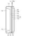
- FIG. 3 is a side view of the semiconductor laser device 1 according to the embodiment. Note that the insulating film 81 is omitted in FIG.
- a semiconductor laser device 1 has a front facet 1a and a rear facet 1b, which are cavity facets, and a first side face 1c and a second side face 1d, which are faces intersecting the cavity facets.
- the front facet 1a is a facet on the front side of the semiconductor laser element 1, and is a cavity facet from which laser light is emitted.
- the rear facet 1b is a facet on the rear side of the semiconductor laser element 1, and is a cavity facet from which laser light is not emitted.
- the front facet 1a and the rear facet 1b face each other as a pair of resonator facets.
- the rear end face 1b is the end face opposite to the front end face 1a.
- the first side face 1c is one side face of the semiconductor laser element 1.
- the second side surface 1 d is the other side surface of the semiconductor laser element 1 .
- the first side surface 1c and the second side surface 1d face each other as a pair of side surfaces.
- the first side surface 1c and the second side surface 1d are surfaces orthogonal to the front end surface 1a and the rear end surface 1b.
- the semiconductor laser device 1 has a substrate 10 and a semiconductor lamination structure 20 formed on one surface of the substrate 10 .
- the semiconductor laminated structure 20 is a structure in which a plurality of semiconductor layers are laminated, and has a PN junction.
- the semiconductor laser element 1 in this embodiment is a nitride semiconductor laser made of a nitride-based semiconductor material. Therefore, the semiconductor laminated structure 20 is a nitride semiconductor laminated body in which a plurality of nitride semiconductor layers each made of a nitride semiconductor material are laminated. Specifically, the semiconductor laser device 1 is a GaN-based nitride semiconductor laser. Laser light emitted from the semiconductor laser element 1 is, for example, light in a wavelength band from ultraviolet to blue.
- the semiconductor laser device 1 has an optical waveguide with a front facet 1a and a rear facet 1b as resonator reflection mirrors.
- the semiconductor laminated structure 20 has an optical waveguide.
- the optical waveguide extends along the resonator length direction of the semiconductor laser device 1 .
- the semiconductor laminated structure 20 is formed with a ridge portion 20a as an optical waveguide. Therefore, the ridge portion 20a is formed so as to extend along the cavity length direction of the semiconductor laser device 1 .
- the ridge portion 20 a has a convex shape and is formed by digging the semiconductor laminated structure 20 .
- the semiconductor laser element 1 has a shape elongated in the cavity length direction.
- the length of the semiconductor laser device 1 in the cavity length direction is, for example, 800 ⁇ m or more, and is 1200 ⁇ m in this embodiment.
- a laser resonator is formed by the front facet 1a and the rear facet 1b. Therefore, the rear facet 1b has a higher reflectance than the front facet 1a. As an example, the reflectance of the front facet 1a is 5%, and the reflectance of the rear facet 1b is 95%.
- a first coating film 31 is formed as a reflective film on the front side of the semiconductor laser device 1, and a second coating film 31 is formed on the rear side of the semiconductor laser device 1 as a reflective film.
- a two-coat film 32 is formed.
- the first coat film 31 is formed on the front end face of the semiconductor laminated structure 20
- the second coat film 32 is formed on the rear end face of the semiconductor laminated structure 20 .
- the first coat film 31 and the second coat film 32 are composed of a dielectric multilayer film in which a plurality of dielectric films are laminated.
- the film thickness of the second coat film 32 on the rear side is larger than the film thickness of the first coat film 31 on the front side.
- the film thickness of the second coat film 32 is at least twice as large as the film thickness of the first coat film 31, and is approximately eight times as large in the present embodiment.
- the substrate 10 is a semiconductor substrate made of GaN, SiC, or the like, or an insulating substrate such as a sapphire substrate.
- the substrate 10 is, for example, an n-type GaN substrate made of hexagonal GaN single crystal.
- an n-type GaN substrate having a (0001) plane as the main surface is used as the substrate 10.
- the semiconductor laminated structure 20 has an n-side first semiconductor layer 21, an active layer 22, and a p-side second semiconductor layer 23 on the substrate 10 in this order.
- the active layer 22 is a PN junction in the semiconductor laminated structure 20 .
- the first semiconductor layer 21, the active layer 22, and the second semiconductor layer 23 are formed by epitaxially growing a nitride-based semiconductor material using a metal organic chemical vapor deposition (MOCVD) method. can be done.
- MOCVD metal organic chemical vapor deposition
- the first semiconductor layer 21 includes at least an n-type clad layer.
- the first semiconductor layer 21 has an n-side clad layer including an n-type clad layer and an n-side optical guide layer formed on the n-side clad layer.
- the n-side cladding layer and the n-side optical guide layer may be either a single layer or multiple layers.
- the n-side clad layer is an n-side clad layer (n-AlGaN layer) made of AlGaN doped with silicon.
- the n-side optical guide layer is an optical guide layer (un-GaN layer) made of undoped GaN.
- the active layer 22 is a quantum well active layer.
- the active layer 22 has a laminated structure in which well layers (well layers) made of undoped InGaN and barrier layers (barrier layers) made of undoped InGaN are alternately laminated.
- the active layer 22 may have either a single quantum well structure (SQW) or a multiple quantum well structure (MQW).
- the active layer 22 has a five-layer structure including a barrier layer made of InGaN, a well layer made of InGaN, a barrier layer made of InGaN, a well layer made of InGaN, and a barrier layer made of InGaN. be.
- the second semiconductor layer 23 includes at least a p-type clad layer.
- the second semiconductor layer 23 includes a p-side optical guide layer, an OFS layer (overflow suppression layer) formed on the p-side optical guide layer, and an OFS layer formed on the p-type optical guide layer. It has a p-side clad layer including a clad layer and a contact layer formed on the p-side clad layer.
- the p-side optical guide layer, OFS layer, p-side cladding layer and contact layer may be either a single layer or multiple layers.
- the p-side optical guide layer is a p-side optical guide layer (un-GaN layer) made of undoped GaN.
- the OFS layer is a p-type OFS layer (p-AlGaN layer) made of AlGaN doped with magnesium as an impurity.
- the p-side clad layer is a p-type p-side clad layer (p-AlGaN layer) doped with magnesium as an impurity.
- the contact layer is a p-type contact layer (p-GaN layer) made of GaN doped with magnesium as an impurity.
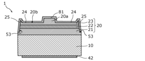
- a concave portion 24 is formed in the semiconductor laminated structure 20 configured as described above, as shown in FIGS. 1 to 2C.
- the semiconductor laminated structure 20 is formed with a ridge portion 20a and a flat portion 20b extending laterally from the base of the ridge portion 20a.
- the recess 24 is formed by digging the semiconductor laminated structure 20 by etching. As shown in FIGS. 2A to 2C, in the present embodiment, the recess 24 digs into the second semiconductor layer 23 . That is, the ridge portion 20 a and the flat portion 20 b are formed in the second semiconductor layer 23 .
- the ridge portion 20a is formed in the p-side clad layer and the contact layer.
- the ridge portion 20a is composed of a convex portion formed on the p-side clad layer and a contact layer formed on the convex portion, and the uppermost layer of the ridge portion 20a is the contact layer.
- the flat portion 20b is formed in the p-side clad layer. The flat surface of the flat portion 20 b is the bottom of the recess 24 and the surface of the p-side clad layer in the recess 24 .
- the width and height of the ridge portion 20a are not particularly limited, but as an example, the ridge width (stripe width) of the ridge portion 20a is 1 ⁇ m or more and 100 ⁇ m or less, and the height of the ridge portion 20a is 100 nm or more and 1000 nm. It is below. Although the width of the contact layer is the same as the ridge width of the ridge portion 20a, it is not limited to this.
- the semiconductor laminated structure 20 is further formed with convex wings 20c. ing. That is, the semiconductor laminated structure 20 has the ridge portion 20a and the wing portions 20c as the convex structure.
- recess 24 is formed by digging second semiconductor layer 23 . Therefore, the wing portion 20c is composed of the second semiconductor layer 23 and has the same height as the ridge portion. Specifically, the wing portion 20c is composed of a p-side clad layer and a contact layer, like the ridge portion 20a. The top surfaces of the ridge portion 20a and the wing portions 20c are both flat.
- the wing portions 20c are formed on both sides of the ridge portion 20a. That is, the semiconductor laminated structure 20 has a pair of wing portions 20c. The ridge portion 20a is sandwiched between the pair of wing portions 20c with the recess 24 interposed therebetween. The pair of wing portions 20c extends along the cavity length direction of the semiconductor laser device 1, similarly to the ridge portion 20a. Thus, by providing the wing portions 20c on both sides of the ridge portion 20a, it is possible to reduce the pressure applied to the ridge portion 20a when the semiconductor laser device 1 is junction-down mounted.
- the width of each of the pair of wing portions 20c is larger than the width of the ridge portion 20a, but the width is not limited to this. Also, the widths of the pair of wing portions 20c are the same as each other, but may be different.
- wingless portions 20d in which the wing portions 20c are not formed are formed in the vicinity of the end faces of the semiconductor laminated structure 20. As shown in FIG. That is, the wingless portion 20d is part of the recess 24. As shown in FIG. In the present embodiment, the wingless portion 20d is formed in the vicinity of each of the front end surface and the rear end surface of the semiconductor laminated structure 20. As shown in FIG.
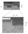
- projections 25 are formed on the surface of the edge of the semiconductor laminated structure 20 in the wingless portion 20d in the direction orthogonal to the resonator length direction.
- the protrusion 25 is formed at the boundary between the surface of the semiconductor laminated structure 20 and the side surface of the second groove 52, which will be described later.
- the edge of the semiconductor laminated structure 20 where the protrusion 25 is formed becomes the boundary between the surface of the semiconductor laminated structure 20 and the side surface of the second groove 52 .
- the protrusion 25 is also formed at the boundary between the surface of the semiconductor laminated structure 20 and the side surface of the third groove 53, which will be described later.
- the edge of the semiconductor laminated structure 20 where the protrusion 25 is formed becomes the boundary between the surface of the semiconductor laminated structure 20 and the side surface of the third groove 53 .
- the protrusion 25 is formed in a horn shape with a triangular cross section.
- a p-side electrode 41 is formed on the ridge portion 20a of the second semiconductor layer 23, as shown in FIG. 2B. Specifically, the p-side electrode 41 is formed on the contact layer. In this embodiment, the p-side electrode 41 is formed only on the upper surface of the ridge portion 20a. The width of the p-side electrode 41 is narrower than the width of the ridge portion 20a, but may be the same as the width of the ridge portion 20a.
- the p-side electrode 41 is formed using at least one metal material such as Pt, Ti, Cr, Ni, Mo and Au, for example.
- the p-side electrode 41 may be either a single layer or multiple layers.
- the p-side electrode 41 is an electrode having a two-layer structure of a Pd layer made of Pd and having a thickness of 40 nm and a Pt layer made of Pt and having a thickness of 35 nm.
- a pad electrode may be formed on the p-side electrode 41 .
- an n-side electrode 42 is formed on the lower surface (rear surface), which is the other surface of the substrate 10 .
- the n-side electrode 42 is an ohmic electrode that makes ohmic contact with the substrate 10, which is a semiconductor substrate.
- the n-side electrode 42 is made of, for example, at least one metal material such as Cr, Ti, Ni, Pd, Pt, Au, and Ge. Also, the n-side electrode 42 may be either a single layer or multiple layers.
- the semiconductor laminated structure 20 is covered with an insulating film 81 made of a dielectric film such as SiO 2 or SiN, except for the p-side electrode 41 on the ridge portion 20a.
- the insulating film 81 is formed to cover the second semiconductor layer 23 except for the upper surface of the ridge portion 20a. That is, the insulating film 81 is formed so as to have an opening on the ridge portion 20a of the contact layer.
- the insulating film 81 functions as a current blocking film. Therefore, the opening of the insulating film 81 serves as a current injection window through which current passes. Note that the insulating film 81 may be formed up to the side surface of the semiconductor laminated structure 20 .
- a pad electrode 82 is formed on the p-side electrode 41 .
- the pad electrode 82 is in contact with the p-side electrode 41 .
- the pad electrode 82 is wider than the ridge portion 20a and is formed on the wing portion 20c. That is, the pad electrode 82 is formed on the insulating film 81 so as to cover the ridge portion 20a, the flat portion 20b (recess 24) and the wing portion 20c.
- the pad electrode 82 is made of a metal material such as Au.
- the pad electrode 82 may be formed via an adhesion auxiliary layer such as Ti. In this case, the adhesion auxiliary layer may also be part of the pad electrode 82 .
- a plurality of grooves are formed in the semiconductor laser element 1 configured as described above. Specifically, as shown in FIGS. 1 to 3, the semiconductor laser element 1 is formed with a first groove 51, a second groove 52 and a third groove 53 as a plurality of grooves.
- the first groove 51 is formed on the back side of the semiconductor laser element 1 . Specifically, the first groove 51 is formed on the back surface of the substrate 10 .
- the second groove 52 and the third groove 53 are formed on the front side of the semiconductor laser element 1 . Specifically, the second groove 52 and the third groove 53 are formed in the semiconductor laminated structure 20 .
- a first groove 51 formed in the back surface of the substrate 10 is a guide groove when dividing a wafer in which a plurality of semiconductor layers are laminated. Specifically, as will be described later, the first grooves 51 are used when dividing each of a plurality of bar-shaped substrates after dividing a semiconductor laminated substrate in which a plurality of semiconductor layers are laminated on a wafer. It is a guide groove.
- the first groove 51 is a scribed groove, and can be formed, for example, by irradiating the back surface of the substrate 10 with laser light.
- the stress applied to the semiconductor laser element 1 during the division into individual pieces can be reduced, so that the occurrence of cracks can be suppressed. .
- the first groove 51 is formed to extend in the direction of the cavity of the semiconductor laser device 1 . Also, the first groove 51 is formed on each of the pair of side surfaces of the semiconductor laser element 1 . That is, a pair of first grooves 51 are formed in the semiconductor laser element 1 . As shown in FIG. 2B, each of the pair of first grooves 51 is formed by cutting the side surface of the semiconductor laser element 1 from the back surface of the substrate 10 . A pair of first grooves 51 are formed in the side surfaces of the substrate 10 . Specifically, one of the pair of first grooves 51 extends along the resonator length direction so as to cut one side surface of the substrate 10 corresponding to the first side surface 1c. The other of the pair of first grooves 51 extends along the resonator length direction so as to cut out the other side of the substrate 10 corresponding to the second side 1d.
- both ends of each of the pair of first grooves 51 in the cavity length direction are located at positions recessed from the end faces of the semiconductor laminated structure 20 . That is, each first groove 51 is formed so that both end portions in the resonator length direction do not reach the end face of the semiconductor laminated structure 20 . Specifically, in the vicinity of the front end of the semiconductor laminated structure 20, the first groove 51 is located between the rear end of the first groove 51 in the cavity length direction and the rear end face of the semiconductor laminated structure 20. There is a portion (remaining white space) in which the semiconductor laminated structure 20 is left without forming the .
- the first groove 51 is provided between the front end of the first groove 51 in the cavity length direction and the front end surface of the semiconductor laminated structure 20 . There is a portion (remaining white space) where the semiconductor laminated structure 20 is left without being formed.
- the bottom of the first groove 51 is positioned inside the substrate 10 . That is, the first groove 51 is formed so as not to reach the semiconductor laminated structure 20 on the upper surface side of the substrate 10 from the lower surface (back surface) of the substrate 10 .
- the thickness of the substrate 10 is 83 ⁇ m
- the depth of the first groove is 55 ⁇ m
- the remaining margin is 13 ⁇ m.
- the second grooves 52 formed in the semiconductor laminated structure 20 are crack prevention grooves for preventing cracks from progressing when dividing the bar-shaped substrate into individual pieces.
- the second groove 52 can be formed by etching the semiconductor laminated structure 20 .
- the second groove 52 is formed along the cavity direction of the semiconductor laser element 1 from the end surface of the semiconductor laminated structure 20 .
- second groove 52 is formed from the rear end surface of semiconductor laminated structure 20 toward the front end surface.
- the second groove 52 is formed only in the vicinity of the rear end surface of the semiconductor laminated structure 20 .
- the second groove 52 is formed in the wingless portion 20d of the semiconductor laminated structure 20, but may be formed across the wing portion 20c.
- the second groove 52 may also be formed near the front end surface of the semiconductor laminated structure 20 .
- the second grooves 52 are formed on both sides of the ridge portion 20a, which is the optical waveguide, when viewed from above.
- a pair of second grooves 52 are formed in the semiconductor laser element 1 .
- Each of the pair of second grooves 52 is formed between the first groove 51 and the ridge portion 20a.
- one of the pair of second grooves 52 is formed between one of the pair of first grooves 51 and the ridge portion 20a in the direction orthogonal to the resonator length direction of the semiconductor laser element 1.
- the other of the pair of second grooves 52 is formed between the other of the pair of first grooves 51 and the ridge portion 20a in the direction orthogonal to the resonator length direction of the semiconductor laser element 1. As shown in FIG.
- the length of the second groove 52 in the cavity length direction is preferably 1/2 or more of the distance (remaining space) between the first groove 51 and the rear end surface of the semiconductor laminated structure 20 .
- the length of the second groove 52 in the resonator length direction is 10 ⁇ m or more from the rear end surface of the semiconductor laminated structure 20 and is 25 ⁇ m or more, which is the distance between the third groove 53 and the second groove 52 . less than double.
- the length of the second groove 52 in the cavity length direction is 14 ⁇ m for the semiconductor laser device 1 whose length in the cavity length direction is 1200 ⁇ m.
- the lengths of the pair of second grooves 52 in the resonator direction are the same, but may be different.
- the width of the second groove 52 is, for example, 10 ⁇ m or less. In the present embodiment, the width of each second groove 52 is 8 ⁇ m, but it may be narrower as long as it can be etched. The widths of the pair of second grooves 52 are the same, but may be different.
- the depth of the second groove 52 is deeper than the portion of the surface of the semiconductor laminated structure 20 that is closest to the substrate 10 .
- the portion of the surface of semiconductor laminated structure 20 closest to substrate 10 is the bottom of third groove 53 . That is, as shown in FIG. 2C, the depth of each second groove 52 is deeper than the depth of the third groove 53 .
- the bottom of the second groove 52 is positioned about 2 ⁇ m below the portion of the surface of the semiconductor laminated structure 20 that is closest to the substrate 10 .
- the depth of the second groove 52 may be equal to the depth of the third groove 53 .
- the depths of the pair of second grooves 52 are the same as each other, they may be different.
- the side surface (inner surface) of the second groove 52 is inclined. Specifically, each of the pair of opposed side surfaces of the second groove 52 is inclined. In the present embodiment, the second groove 52 is tapered so that the width of the groove gradually narrows along the depth direction.
- the third groove 53 formed in the semiconductor laminated structure 20 serves to separate the laminated semiconductor layers for each optical waveguide in a semiconductor laminated substrate in which a plurality of semiconductor layers are laminated on a wafer by epitaxial growth. It is an isolation trench (element isolation trench). Therefore, as shown in FIGS. 2A to 2C, the third grooves 53 are formed on each of the pair of side surfaces of the semiconductor laser element 1. As shown in FIGS. In other words, a pair of third grooves 53 are formed in the semiconductor laser element 1 .
- the third groove 53 can be formed by etching a plurality of laminated semiconductor layers.
- Each of the pair of third grooves 53 is formed so as to cut the side surface of the semiconductor laminated structure 20 from the upper surface of the semiconductor laminated structure 20 . Further, as shown in FIG. 1, the third groove 53 is formed so as to extend in the cavity direction of the semiconductor laser device 1 . Specifically, one of the pair of third grooves 53 extends along the resonator length direction so as to cut one side surface of the semiconductor laminated structure 20 . The other of the pair of third grooves 53 extends along the resonator length direction so as to cut out the other side surface of the semiconductor laminated structure 20 . In the present embodiment, the pair of third grooves 53 are both formed from the front end face to the rear end face of the semiconductor laminated structure 20 .
- the third groove 53 can be formed by digging from the upper surface of the semiconductor laminated structure 20 in the lamination direction. As shown in FIGS. 2A to 2C, the depth of the third groove 53 is deeper than the position of the active layer 22 which is the PN junction in the semiconductor laminated structure 20. As shown in FIGS. Moreover, in the present embodiment, the side surface of the third groove 53 is inclined. Specifically, the side surface of the third groove 53 is slanted so that the skirt widens along the depth direction.
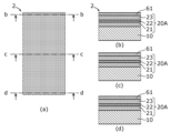
- FIGS. 4A to 4J are diagrams for explaining each step in the method of manufacturing the semiconductor laser device 1 according to the embodiment.
- (a) is a top view of the semiconductor laser device 1
- (b) is a cross-sectional view taken along line bb in (a)
- (c) is a cross-sectional view of (a). It is a cross-sectional view taken along line cc
- (d) is a cross-sectional view taken along line dd of (a).
- 4A to 4J hatching is applied for the sake of convenience in order to make it easier to understand the correspondence of the members seen on the top surface.
- the insulating film 81 is omitted.
- 4A to 4J only show a portion corresponding to one semiconductor laser element 1 of the semiconductor laminated structure 20A formed on the substrate 10, which is a wafer.
- a semiconductor laminated substrate 2 having a semiconductor laminated structure 20A is fabricated by laminating a plurality of semiconductor layers on one surface of a substrate 10, which is a wafer. Specifically, the first semiconductor layer 21, the active layer 22 and the second semiconductor layer 23 are sequentially epitaxially grown on the upper surface of the substrate 10 by the MOCVD method to form the semiconductor laminated structure 20A. After that, an insulating film 61 (first insulating film) is formed on the semiconductor laminated structure 20A. In this embodiment, an SiO 2 film is formed as the insulating film 61 . As an example, the film thickness of the insulating film 61 is 300 nm. Note that the insulating film 61 may not be formed.
- a first resist 71 having a predetermined shape and having a first opening 71a and a second opening 71b is formed above the semiconductor laminated structure 20A.
- the first opening 71a is formed at a position where a second groove 52, which will be described later, is formed.
- the second opening 71b is formed at a position where a third groove 53, which will be described later, is formed.
- the insulating film 61 is formed on the semiconductor laminated structure 20A. Formed on top.
- the semiconductor laminated structure 20A is etched (first etching step). Specifically, the semiconductor laminated structure 20A is etched using the first resist 71 having the first opening 71a and the second opening 71b as a mask. As a result, the recess 52a can be formed in the portion corresponding to the first opening 71a in the semiconductor laminated structure 20A, and the third groove 53 can be formed in the portion corresponding to the second opening 71b in the semiconductor laminated structure 20A. can be formed. Dry etching such as reactive ion etching can be used as an etching method for the semiconductor laminated structure 20A.
- the semiconductor laminated structure 20A is etched such that the bottom of the recess 52a and the bottom of the third groove 53 both reach the middle of the first semiconductor layer 21.
- the recess 52 a and the third groove 53 are formed to penetrate the second semiconductor layer 23 and the active layer 22 and reach the inside of the first semiconductor layer 21 .
- the insulating film 61 is also etched. That is, the recess 52 a and the third groove 53 also penetrate the insulating film 61 .
- the first resist 71 used as a mask is removed. Thereby, the insulating film 61 is exposed.
- a second resist 72 having a predetermined shape and having an opening 72a is formed above the semiconductor laminated structure 20A.
- the opening 72a is formed at a position where the recess 24 to be formed in the semiconductor laminated structure 20A is to be formed.
- openings 72 a of the second resist 72 are also formed at positions corresponding to the second grooves 52 . That is, the opening 72a is formed so as to overlap with the recess 52a formed in the semiconductor laminated structure 20A, and the recess 52a is not covered with the second resist 72.
- the third grooves 53 formed in the semiconductor laminated structure 20A are covered with the second resist 72 .
- the third groove 53 is filled with the second resist 72 .
- the second resist 72 having the opening 72a is formed on the insulating film 61. As shown in FIG.
- the semiconductor laminated structure 20A in which the recess 52a is formed is etched (second etching step). Specifically, the semiconductor laminated structure 20A is etched using the second resist 72 having the opening 72a as a mask. As a result, recesses 24 are formed in the semiconductor lamination structure 20A at portions corresponding to the openings 72a, and the ridge portion 20a and the wing portions 20c are formed in the semiconductor lamination structure 20A. Dry etching such as reactive ion etching can be used as an etching method for the semiconductor laminated structure 20A.
- the semiconductor laminated structure 20A is etched so that the bottom of the concave portion 24 reaches halfway through the second semiconductor layer 23 . That is, the ridge portion 20 a and the wing portions 20 c are formed in the second semiconductor layer 23 .
- the insulating film 61 is formed on the semiconductor laminated structure 20A, the insulating film 61 is also etched. As a result, the insulating film 61 remains only on the ridge portion 20a.
- the recesses 52a formed in the semiconductor laminated structure 20A by the first etching process are not covered with the second resist 72, the recesses 52a are further etched in this etching process. As a result, the bottom of the concave portion 52a is further deepened to form the second groove 52.
- the concave portion 52a formed up to the first semiconductor layer 21 is further etched to dig into the inside of the substrate 10 .
- the second groove 52 is formed using the first etching process for forming the third groove 53 and the second etching process for forming the ridge portion 20a. Therefore, the second grooves 52 can be formed without adding a process only for forming the second grooves 52 . That is, according to the manufacturing method of the present embodiment, it is not necessary to use a mask only for forming the second grooves 52 .
- the second resist 72 used as a mask is removed.
- the insulating film 61 on the ridge portion 20a is exposed, and the second semiconductor layer 23 in which the concave portion 24 is formed is exposed.
- the dry etching of the insulating film 61 which is the first step in forming the ridge portion 20a
- the upper side walls of the second groove 52 and the third groove 53 of the semiconductor laminated structure 20A in the wingless portion 20d are covered with the dry etching process.
- Deposits are formed by accumulating debris. Since this deposit has a slower etching rate than the insulating film 61 (the SiO 2 film in this embodiment), a small amount of the deposit remains on the sidewalls of the second groove 52 and the third groove 53 even after etching. become.
- the residual ions remain on the upper side walls of the second groove 52 and the third groove 53.
- the deposited deposits serve as a mask to form the protrusions 25 . Note that the deposits remaining on the upper side walls of the second groove 52 and the third groove 53 in the first stage are etched by the dry etching of the semiconductor laminated structure 20A and the substrate 10, so during the dry etching in the next stage. will disappear in
- an insulating film 62 (second insulating film) is formed to cover the insulating film 61 on the ridge portion 20a.
- the insulating film 62 is formed so as to cover the entire upper surface of the semiconductor laminated structure 20A.
- an SiO 2 film is formed as the insulating film 62 .
- the film thickness of the insulating film 62 is 200 nm.
- Annealing is then performed to activate the dopant in the p-type semiconductor layer.
- the ridge portion 20a is protected by the two insulating films. As a result, it is possible to prevent the ridge portion 20a from being damaged by the heat of the annealing process.
- the insulating film 62 and the insulating film 61 are removed. As a result, the entire surface of the semiconductor laminated structure 20A having the ridge portion 20a and the wing portions 20c is exposed. Therefore, the second groove 52 and the third groove 53 formed in the semiconductor laminated structure 20A are also exposed.
- FIG. 5 shows a cross-sectional SEM image of a portion corresponding to a region V surrounded by a broken line in (d) of FIG. 4H.
- the depth of the second groove 52 is deeper than the depth of the third groove 53 in FIG. 4H, the depth of the second groove 52 and the depth of the third groove 53 are the same in FIG.
- the semiconductor laser device 1 is shown when it is manufactured.
- the p-side electrode 41 is formed on the ridge portion 20a. Specifically, an insulating film 81 having an opening is formed on the upper surface of the ridge portion 20a, and the p-side electrode 41 is formed so as to cover the upper surface of the ridge portion 20a.
- the p-side electrode 41 can be formed into a predetermined shape using, for example, a vapor deposition method and a lift-off method. After that, a pad electrode 82 is further formed so as to straddle the p-side electrode 41 and the insulating film 81 .
- the n-side electrode 42 is formed on the back surface of the substrate 10. Then, as shown in FIG. 4J, the n-side electrode 42 is formed on the back surface of the substrate 10. Then, as shown in FIG. 4J, the n-side electrode 42 can be formed into a predetermined shape using, for example, a vapor deposition method and a lift-off method.
- the semiconductor laminated substrate 2 is divided to produce a plurality of bar-shaped substrates each having a plurality of optical waveguides (primary division step).
- a plurality of bar-shaped substrates are manufactured by cleaving and dividing the semiconductor laminated substrate 2 .
- a first groove 51 is formed in the rear surface of the semiconductor laminated substrate 2 or the bar-shaped substrate.
- the first grooves 51 are guide grooves for dividing the bar-shaped substrate into a plurality of semiconductor laser elements 1 . Therefore, the first groove 51 is formed at each boundary between two adjacent semiconductor laser elements 1 . That is, the first groove 51 is formed parallel to the longitudinal direction of the ridge portion 20a. Further, the first grooves 51 are located at positions recessed from both end faces when the semiconductor laminated substrate 2 is divided into a plurality of bar-shaped substrates. In other words, the first grooves 51 are formed so as not to reach the positions corresponding to the end faces of the plurality of bar-shaped substrates. Such first grooves 51 can be formed by irradiating the rear surface of the substrate 10 with laser light. Specifically, the first groove 51 is a laser scribed groove formed by a laser scribing method.
- the semiconductor laminated substrate 2 is divided to produce a plurality of bar-shaped substrates
- the first coat film 31 and the second coat film 32 are formed on the end surfaces of the bar-shaped substrates, and then the bars are formed along the first grooves 51 .
- a plurality of semiconductor laser devices 1 each having one optical waveguide (ridge portion 20a) are produced (secondary division step).
- the bar-shaped substrate is divided into a plurality of pieces in the same manner as the method shown in FIG. Thereby, the semiconductor laser device 1 shown in FIGS. 1 to 3 can be obtained. Some of them include those with cracks as shown in FIG.
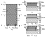
- FIG. 6 (a) is a top view, (b) is a cross-sectional view taken along line bb in (a), and (c) is a cross-sectional view taken along line cc in (a). , (d) is a cross-sectional view taken along line dd of (a), and (e) is a side view of the semiconductor laser device 1 viewed from the rear side with the second coating film 32 omitted.
- a thick line in FIG. 6 indicates a crack 90 generated in the semiconductor laser device 1. As shown in FIG. Since the surface of the crack 90 is inclined, the depth position of the crack 90 on the side surface of the semiconductor laminated structure 20 is deeper than the depth position of the crack 90 on the dd line cross section. Also, the hatched area of dots in FIG. 6(a) indicates the area where the crack 90 occurs.
- the second groove 52 is formed in the semiconductor laminated structure 20 in the semiconductor laser device 1 manufactured as described above.
- the second groove 52 is formed along the resonator length direction from the end face of the semiconductor laminated structure 20 .
- the third groove 53 is formed in the semiconductor laminated structure 20 .
- the third groove 53 extends along the cavity length direction of the semiconductor laser element 1 so as to cut the side surface of the semiconductor laminated structure 20 .
- the depth of the second groove 52 is deeper than the portion of the surface of the semiconductor laminated structure 20 that is closest to the substrate 10 side. Specifically, as shown in (d) and (e) of FIG. 6 , the depth of the second groove 52 is deeper than the depth of the third groove 53 .
- the depth of the second groove 52A and the depth of the third groove 53 are the same, and the crack 90 is generated at a deeper position.
- the average traveling direction of the crack 90 does not intersect with the second groove 52A. change the angle of progression of the crack 90, and as a result, the progression of the crack 90 to the ridge portion 20a may be prevented. Therefore, by making the depth of the second groove 52 greater than or equal to the depth of the third groove 53 , the second groove 52 can effectively prevent the crack 90 from progressing.
- the cracks 90 are often generated from a portion approximately 2 ⁇ m below the portion of the surface of the semiconductor laminated structure 20 closest to the substrate 10 (for example, the upper surface of the third groove 53).
- the depth is preferably 2 ⁇ m or more from the portion of the surface of the semiconductor laminated structure 20 closest to the substrate 10 .
- cracks 90 generated in the cross section perpendicular to the cavity length direction of the semiconductor laser device 1 are formed in the substrate 10 from the side surface of the semiconductor laminated structure 20. It extends obliquely upward at an angle of 1.5° with respect to the main surface.
- the depth of the third groove 53 from the upper surface of the semiconductor laminated structure 20 is A
- the length from the bottom of the third groove 53 to the position of the starting point of the crack 90 in the depth direction is B
- the width of the third groove 53 on the upper surface of the semiconductor laminated structure 20 is C
- the distance from the wall surface of the third groove 53 to the inner surface outside the second groove 52 is D
- the depth of the second groove 52 is 1 ⁇ m, 3 ⁇ m
- the distance between the third groove 53 and the second groove 52 is 9 ⁇ m or less (4 ⁇ m, 7 ⁇ m, 8 ⁇ m, 9 ⁇ m)
- the width of the third groove 53 is is 4 ⁇ m.
- the length Y of the second groove 52 in the cavity length direction from the rear end surface of the semiconductor laminated structure 20 is preferably 25 times or less the distance between the third groove 53 and the second groove 52 . Thereby, it is possible to suppress the occurrence of defects such as chipping in the portion between the third groove 53 and the second groove 52 .
- the depth of the third groove 53 is the same as the depth of the active layer, which is the PN junction of the semiconductor laminated structure 20. It is deeper than the position of 22.
- the semiconductor laser element 1 can be easily separated by the third groove 53 . Further, if the depth of the third groove 53 is shallower than the position of the PN junction, the PN junction may be exposed at the time of individual separation, and leakage may occur at the PN junction. By making the height deeper than the position of the PN junction, it is possible to suppress the occurrence of leakage at the PN junction during separation into individual pieces.
- the depth of the third groove 53 By making the depth of the third groove 53 shallow, the position of the origin of the crack 90 at the corner of the semiconductor laminated structure 20 becomes shallow. In other words, the distance of the crack 90 extending upward from the side surface of the semiconductor laminated structure 20 is shortened.
- the depth of the third groove 53 is 1 ⁇ m to 3 ⁇ m. By reducing the depth of the starting point of the crack 90, the distance for the crack 90 to reach the surface can be shortened.
- the side surfaces of the second groove 52 are inclined.
- the side surface of the third groove 53 is also inclined.
- the angle formed by the upper surface of the semiconductor laminated structure 20 and the side surface of the second groove 52 can be made obtuse.
- the angle formed by the upper surface of the semiconductor laminated structure 20 and the side surface of the third groove 53 can be made obtuse.
- the distance between the second groove 52 and the ridge portion 20a is 4 ⁇ m or more when viewed from above.
- the crack 90 extending obliquely upward from the side surface of the semiconductor laser element 1 (semiconductor laminated structure 20) can be efficiently prevented from progressing by the second groove 52, and current constriction in the lateral direction can be prevented. can be done effectively.
- the second groove 52 can efficiently block the crack 90 progressing obliquely upward on the side farther from the side surface of the semiconductor laser element 1 (semiconductor laminated structure 20). In other words, the second groove 52 should be closer to the ridge portion 20 a than the side surface of the semiconductor laser element 1 .
- the length of the second groove 52 in the resonator length direction is 1/2 or more of the distance between the first groove 51 and the end surface of the semiconductor laminated structure 20 .
- the length of the second groove 52 in the resonator length direction is 14 ⁇ m, and the distance between the first groove 51 and the end surface of the semiconductor laminated structure 20 is 13 ⁇ m.
- the projection 25 is formed on the surface of the edge of the semiconductor laminated structure 20 in the direction orthogonal to the resonator length direction in the wingless portion 20d of the semiconductor laminated structure 20. ing. Specifically, the protrusion 25 is formed on the edge that is the boundary between the surface of the semiconductor laminated structure 20 and the side surface of the second groove 52 . A protrusion 25 is also formed on the edge, which is the boundary between the surface of the semiconductor laminated structure 20 and the side surface of the third groove 53 .
- the height of the protective member is equal to the height of the ridge portion 20a. Therefore, stress applied to the ridge portion 20a at the time of division can be suppressed. As a result, it is possible to suppress the occurrence of chipping (end surface step, etc.) in the ridge portion 20a due to the stress during division.
- the projections 25 are formed on the semiconductor laminated structure 20, the surface area of the semiconductor laminated structure 20 can be increased. As a result, the contact area between the solder and the semiconductor laser element 1 increases when the semiconductor laser element 1 is mounted on the submount by soldering, so that bonding and adhesion can be improved.
- the waveguide in the semiconductor laser device 1 is the ridge portion 20a, but it is not limited to this.
- the waveguide in the semiconductor laser device 1 may have an electrode stripe structure composed only of divided electrodes instead of a ridge stripe structure composed of the ridge portion 20a, or a current confinement structure using a current blocking layer. etc.
- the present invention is not limited to this.
- the present disclosure can also be applied when semiconductor materials other than nitride-based semiconductor materials are used.
- a semiconductor laser element according to the present disclosure is useful as a light source element for various products, including projectors, optical discs, vehicle-mounted headlamps, lighting devices, laser processing devices, and the like.
- Reference Signs List 1 1A semiconductor laser element 1a front facet 1b rear facet 1c first side face 1d second side face 2 semiconductor laminated substrate 10 substrate 20, 20A semiconductor laminated structure 20a ridge portion 20b flat portion 20c wing portion 20d wingless portion 21 first semiconductor Layer 22 Active layer 23 Second semiconductor layer 24 Recess 25 Protrusion 31 First coat film 32 Second coat film 41 P-side electrode 42 N-side electrode 51 First groove 52 Second groove 52a Recess 53 Third groove 61, 62 Insulating film 71 first resist 71a first opening 71b second opening 72 second resist 72a opening 81 insulating film 82 pad electrode 90 crack 101 adhesive sheet 102 protective film 103 blade jig
Landscapes
- Physics & Mathematics (AREA)
- Geometry (AREA)
- Condensed Matter Physics & Semiconductors (AREA)
- General Physics & Mathematics (AREA)
- Electromagnetism (AREA)
- Optics & Photonics (AREA)
- Semiconductor Lasers (AREA)
Abstract
半導体レーザ素子(1)は、基板(10)と、基板(10)の一方の面に形成され、複数の半導体層が積層された半導体積層構造体(20)と、を備え、半導体積層構造体(20)は、半導体レーザ素子(1)の共振器長方向に沿って延在する光導波路を有し、基板(10)の他方の面には、半導体レーザ素子(1)の一対の側面を切り欠くように共振器長方向に沿って延在する一対の第1溝(51)が形成されており、一対の第1溝(51)の各々における共振器長方向における両端部は、半導体積層構造体(20)の端面から後退した位置に存在し、半導体積層構造体(20)には、半導体積層構造体(20)の端面から共振器長方向に沿って第2溝(52)が形成されており、上面視において、第2溝(52)は、光導波路の両側に形成され、且つ、第1溝(51)と光導波路との間に形成されている。
Description
本開示は、半導体レーザ素子及び半導体レーザ素子の製造方法に関する。
半導体レーザ素子は、長寿命、高効率及び小型等のメリットがあるため、プロジェクタ、光ディスク、車載ヘッドランプ、照明装置又はレーザ加工装置等の様々な製品の光源に用いられている。近年、半導体レーザ素子として、紫外から青色までの波長帯をカバーすることができる窒化物系半導体レーザの研究開発が進められている。
半導体レーザ素子は、ウエハの上に複数の半導体層が積層された半導体積層基板を分割することで複数のバー状基板を切り出し、さらに、このバー状基板を複数に分割して個片化することで作製することができる。このような分割工程においては、予定の分割線から逸れて分割されてしまったり一部が欠けてしまったりする等の不具合が発生する。
特に、窒化物系半導体レーザは、光ピックアップ又は光通信で使われていた砒化ガリウム系レーザとは異なり、分割工程においては、劈開面ではない結晶面で分割を行っているため、予定の分割線から逸れて分割されてしまったり一部が欠けたりする等の不具合が発生しやすい。
そこで、従来、ガイド溝を用いてウエハを分割して半導体レーザ素子を作製する技術が提案されている。例えば、特許文献1には、複数の半導体層が積層されたウエハの裏面にレーザ光を照射して分割用の溝を形成することで、ウエハを分割する方法が開示されている。
しかしながら、特許文献1に開示された方法を用いたとしても、ウエハの上に複数の半導体層が積層された半導体積層基板を分割する分割工程又は半導体積層基板を分割したバー状基板を分割する分割工程において半導体レーザ素子にクラックが発生し、半導体レーザ素子の信頼性が低下するという課題がある。
本開示は、このような課題を解決するためになされたものであり、製造工程中で発生するクラックにより信頼性が低下することを抑制できる半導体レーザ素子及びその半導体レーザ素子の製造方法を提供することを目的とする。
上記目的を達成するために、本開示に係る第1の半導体レーザ素子の一態様は、共振器端面と前記共振器端面に交差する一対の側面とを有する半導体レーザ素子であって、基板と、前記基板の一方の面に形成され、複数の半導体層が積層された半導体積層構造体と、を備え、前記半導体積層構造体は、前記半導体レーザ素子の共振器長方向に沿って延在する光導波路を有し、前記基板の他方の面には、前記一対の側面を切り欠くように前記共振器長方向に沿って延在する一対の第1溝が形成されており、前記一対の第1溝の各々における前記共振器長方向における両端部は、前記半導体積層構造体の端面から後退した位置に存在し、前記半導体積層構造体には、前記半導体積層構造体の端面から前記共振器長方向に沿って第2溝が形成されており、上面視において、前記第2溝は、前記光導波路の両側に形成され、且つ、前記第1溝と前記光導波路との間に形成されている。
また、本開示に係る第2の半導体レーザ素子の一態様は、基板と、前記基板の一方の面に形成され、複数の半導体層が積層された半導体積層構造体と、を備え、前記半導体積層構造体は、前記半導体レーザ素子の共振器長方向に延在するリッジ部と、前記リッジ部の両側に前記リッジ部と同じ高さで形成されるウイング部とを有し、前記半導体積層構造体の端面の近傍には、前記ウイング部が形成されていないウイングレス部が形成されており、前記ウイングレス部における前記半導体積層構造体の前記共振器長方向に直交する方向の端縁の表面に、突起が形成されている。
また、本開示に係る半導体レーザ素子の製造方法の一態様は、基板の一方の面に複数の半導体層を積層することで半導体積層構造体を有する半導体積層基板を作製する工程と、前記半導体積層構造体をエッチングする第1エッチング工程と、前記第1エッチング工程の後に、前記半導体積層構造体をエッチングする第2エッチング工程と、前記半導体積層基板を分割することで、各々が複数の光導波路を有する複数のバー状基板を作製する分割工程と、前記半導体積層基板又は前記バー状基板の裏面に第1溝を形成する工程と、前記第1溝に沿って前記バー状基板を分割することで、各々が1つの光導波路を有する複数の半導体レーザ素子を作製する分割工程と、を含み、前記第1エッチング工程では、前記半導体積層構造体に凹部を形成し、前記第2エッチング工程では、前記凹部をさらにエッチングして第2溝を形成するとともに、前記光導波路として前記半導体積層構造体にリッジ部を形成し、上面視において、前記第2溝は、前記光導波路の両側において、前記半導体積層構造体の端面から前記半導体レーザ素子の共振器長方向に沿って延在するように形成されており、且つ、前記第1溝と前記光導波路との間に形成されている。
本開示によれば、製造工程中で発生するクラックにより信頼性が低下することを抑制できる半導体レーザ素子を得ることができる。
(本開示の一態様を得るに至った経緯)
まず、本開示の実施の形態を説明することに先立ち、本開示の一態様を得るに至った経緯を説明する。
まず、本開示の実施の形態を説明することに先立ち、本開示の一態様を得るに至った経緯を説明する。
一般的に、半導体レーザ素子を量産する場合、ウエハである基板の上に複数の半導体層が積層された半導体積層基板を分割することで複数本のバー状基板を作製し(一次分割工程)、このバー状基板の両端面にコート膜を形成した後に、バー状基板をさらに複数に分割する個片分割を行うことで複数の半導体レーザ素子に分離する(二次分割工程)。これにより、1枚のウエハからレーザチップとなる複数の半導体レーザ素子を得ることができる。
従来、バー状基板を個片分割する際、半導体積層基板又はバー状基板に予め分割用の溝(ガイド溝)を形成しておいて、この溝に沿ってバー状基板を複数に分割する方法が提案されている。この場合、特許文献1に開示された方法を用いて、分割用の溝を形成することが考えられる。具体的には、半導体積層基板又はバー状基板の裏面にレーザ光を照射することで、分割用の溝を形成することが考えられる。このとき、溝を形成する際のレーザ光によって半導体レーザ素子の共振器端面が熱損傷を受けないようにするために、溝の共振器方向の端部が共振器端面から後退した位置となるようにレーザ光を照射する。つまり、バー状基板のフロント側及びリア側の共振器端面となる位置まで分割用の溝が到達しないようにレーザ光を照射している。
しかしながら、このような方法によって本願発明者らが実際に半導体レーザ素子を作製してみたところ、バー状基板を複数に分割する個片分割工程において、半導体レーザ素子にクラックが生じることが分かった。この点について、以下詳細に説明する。
図8に示すように、基板10Xの裏面に分割用の溝51Xが形成されたバー状基板3Xを粘着シート101と保護フィルム102とで挟んで、分割用の溝51Xに対応する位置においてバー状基板3Xの上からカッター等の刃状治具103を順次押し込んでいく。これにより、バー状基板3Xを複数に分割して、複数の半導体レーザ素子1Xを得ることができる。
このとき、得られた半導体レーザ素子1Xを観察すると、図9に示すように、半導体レーザ素子1Xにおける共振器端面と側面との角部において、基板10Xと半導体積層構造体20Xとの界面近傍からリッジ部20aの下方に向かって斜め上方に伸びるクラック90Xが発生することが分かった。このように、クラック90Xがリッジ部20aの下方にまで延在すると、半導体レーザ素子1Xの信頼性が低下することになる。
なお、図9は、特許文献1の方法によって作製したときの比較例の半導体レーザ素子1Xの構成を示す図である。図9において、(a)は、半導体レーザ素子1Xの上面図であり、(b)は、(a)のb-b線における断面図であり、(c)は、(a)のc-c線における断面図である。図9の(d)は、端面のコート膜32Xを省略して半導体レーザ素子1Xを後端面側から見たときの側面図である。また、図9における太線は、半導体レーザ素子1Xに発生したクラック90Xを示しており、図9の(a)におけるドットのハッチング領域は、クラック90Xが発生した領域を示している。
得られた複数の半導体レーザ素子1Xを調べてみると、図9の(a)に示すように、クラック90Xは、三角形の面状に広がって発生することが分かった。具体的には、図9の(b)及び(d)に示すように、発生する多くのクラック90Xは、半導体レーザ素子1Xの共振器長方向に直交する断面では、半導体積層構造体20Xの側面から、まず溝51X近傍では斜め上方にクラックが進行した後、溝51Xから離れたところでは基板10Xの主面に対して約1.5°の角度でやや斜め上方に向かって伸びるとともに、半導体レーザ素子1Xの側面と平行な断面では、半導体積層構造体20Xの端面から基板10Xの主面に対して約16°の角度で斜め上方に向かって伸びることが分かった。さらに、多くのクラック90Xは、半導体積層構造体20Xの表面のうち最も基板10X側に位置する部分(図9(d)では、分離溝53Xの上面)から2μm程度下方の部分を起点にして発生することも分かった。しかも、クラック90Xは、特に半導体レーザ素子1の後端面側に多く発生することも分かった。
なお、刃状治具103(図8参照)により分割された左右2つの半導体レーザ素子1Xは、いずれにおいても、左側の側面を起点にクラック90Xが発生することが多かったが、右側の側面を起点にクラック90Xが発生することもあった。また、クラック90Xは、上面視において、溝51Xに重なる位置まで伸びていないが、溝51Xに重なる位置まで伸びる場合もあった。
このようにクラック90Xが発生する原因について本願発明者らが検討したところ、個片分割するための分割用の溝51Xを基板10Xの裏面に形成したことと、その分割用の溝51Xをフロント側及びリア側の共振器端面となる位置まで達しないように形成したことで、共振器端面近傍が割れにくくなったことが原因であると推測した。
また、共振器端面のリア側に形成するコート膜32Xの膜厚は、レーザ光をフロント方向に出射させるために、共振器端面のフロント側に形成するコート膜31Xの膜厚に比べて厚くなっている(例えば約8倍程度)ことから、リア側の共振器端面近傍がフロント側の共振器端面に比べて割れにくくなっている。このため、リア側の共振器端面にクラック90Xが多く発生したと考えられる。
そこで、このような課題に対して、本願発明者らが鋭意検討した結果、個片分割の際にクラック90Xが発生したとしても、クラック90Xがリッジ部20aの下方にまで進行することを阻止する構造を設けるという着想を得た。具体的には、半導体積層構造体20Xに、クラック90Xの進行を阻止するための溝を形成するという着想を得た。
このように、本開示は、クラック発生の課題に対してなされたものであり、個片分割の際にクラックが発生したとしても、クラックがリッジ部の下方にまで進行することを抑制できる半導体レーザ素子を得ることを第1の目的とする。
また、ウエハを分割する分割工程(一次分割工程、二次分割工程)では、ウエハの上にSiO2等の保護部材を載置することがあるが、この場合、半導体レーザ素子のリッジ部20aに分割時の応力がかかってリッジ部に欠け(端面段差等)が発生することがある。
本開示は、このような課題に対してもなされたものであり、分割工程の際にリッジ部となる部分にクラックが発生することを抑制できる半導体レーザ素子を得ることを第2の目的とする。
以下、本開示の実施の形態について、図面を参照しながら説明する。なお、以下に説明する実施の形態は、いずれも本開示の一具体例を示すものである。したがって、以下の実施の形態で示される、数値、形状、材料、構成要素、構成要素の配置位置及び接続形態、並びに、ステップ(工程)及びステップの順序等は、一例であって本開示を限定する主旨ではない。よって、以下の実施の形態における構成要素のうち、本開示の最上位概念を示す独立請求項に記載されていない構成要素については、任意の構成要素として説明される。
また、各図は、模式図であり、必ずしも厳密に図示されたものではない。したがって、各図において縮尺等は必ずしも一致していない。各図において、実質的に同一の構成に対しては同一の符号を付しており、重複する説明は省略又は簡略化する。
また、本明細書において、「上方」及び「下方」という用語は、絶対的な空間認識における上方向(鉛直上方)及び下方向(鉛直下方)を指すものではなく、積層構成における積層順を基に相対的な位置関係により規定される用語として用いる。また、「上方」及び「下方」という用語は、2つの構成要素が互いに間隔をあけて配置されて2つの構成要素の間に別の構成要素が存在する場合のみならず、2つの構成要素が互いに接する状態で配置される場合にも適用される。
(実施の形態)
まず、実施の形態に係る半導体レーザ素子1の構成について、図1~図3を用いて説明する。図1は、実施の形態に係る半導体レーザ素子1の上面図である。図2A~図2Cは、実施の形態に係る半導体レーザ素子1の断面図である。図2Aは、図1のIIA-IIA線における断面図であり、図2Bは、図1のIIB-IIB線における断面図であり、図2Cは、図1のIIC-IIC線における断面図である。図3は、実施の形態に係る半導体レーザ素子1の側面図である。なお、図1において、絶縁膜81は省略している。
まず、実施の形態に係る半導体レーザ素子1の構成について、図1~図3を用いて説明する。図1は、実施の形態に係る半導体レーザ素子1の上面図である。図2A~図2Cは、実施の形態に係る半導体レーザ素子1の断面図である。図2Aは、図1のIIA-IIA線における断面図であり、図2Bは、図1のIIB-IIB線における断面図であり、図2Cは、図1のIIC-IIC線における断面図である。図3は、実施の形態に係る半導体レーザ素子1の側面図である。なお、図1において、絶縁膜81は省略している。
図1に示すように、半導体レーザ素子1は、各々が共振器端面である前端面1a及び後端面1bと、各々が共振器端面に交差する面である第1側面1c及び第2側面1dとを有する。
前端面1aは、半導体レーザ素子1のフロント側の端面であり、レーザ光が出射する共振器端面である。後端面1bは、半導体レーザ素子1のリア側の端面であり、レーザ光が出射しない共振器端面である。前端面1aと後端面1bとは、一対の共振器端面として、互いに対向している。後端面1bは、前端面1aとは反対側の端面である。
第1側面1cは、半導体レーザ素子1の側方の一方の面である。第2側面1dは、半導体レーザ素子1の側方の他方の面である。第1側面1cと第2側面1dとは、一対の側面として、互いに対向している。第1側面1c及び第2側面1dは、前端面1a及び後端面1bに直交する面である。
図1~図3に示すように、半導体レーザ素子1は、基板10と、基板10の一方の面である上面に形成された半導体積層構造体20とを有する。半導体積層構造体20は、複数の半導体層が積層された構造であり、PN接合部を有する。
本実施の形態における半導体レーザ素子1は、窒化物系半導体材料によって構成された窒化物半導体レーザである。したがって、半導体積層構造体20は、各々が窒化物系半導体材料を用いて作製された複数の窒化物半導体層が積層された窒化物半導体積層体である。具体的には、半導体レーザ素子1は、GaN系の窒化物半導体レーザである。半導体レーザ素子1から出射するレーザ光は、例えば、紫外から青色までの波長帯域の光である。
半導体レーザ素子1は、前端面1aと後端面1bとを共振器反射ミラーとする光導波路を有する。具体的には、半導体積層構造体20が光導波路を有する。光導波路は、半導体レーザ素子1の共振器長方向に沿って延在している。本実施の形態では、半導体積層構造体20には、光導波路としてリッジ部20aが形成されている。したがって、リッジ部20aは、半導体レーザ素子1の共振器長方向に沿って延在するように形成されている。リッジ部20aは、凸状であり、半導体積層構造体20を掘り込むことで形成されている。なお、半導体レーザ素子1は、共振器長方向に長尺をなす形状になっている。半導体レーザ素子1の共振器長方向の長さは、一例として、800μm以上であり、本実施の形態では、1200μmである。
半導体レーザ素子1では、前端面1aと後端面1bとによってレーザ共振器が形成されている。このため、後端面1bは、前端面1aよりも反射率が高くなっている。一例として、前端面1aの反射率は、5%であり、後端面1bの反射率は、95%である。
具体的には、図1に示すように、半導体レーザ素子1のフロント側には、反射膜として第1コート膜31が形成されており、半導体レーザ素子1のリア側には、反射膜として第2コート膜32が形成されている。第1コート膜31は、半導体積層構造体20の前端面に形成されており、第2コート膜32は、半導体積層構造体20の後端面に形成されている。第1コート膜31及び第2コート膜32は、複数の誘電体膜が積層された誘電体多層膜によって構成されている。本実施の形態において、リア側の第2コート膜32の膜厚は、フロント側の第1コート膜31の膜厚よりも厚くなっている。一例として、第2コート膜32の膜厚は、第1コート膜31の膜厚の2倍以上であり、本実施の形態では、約8倍になっている。
基板10は、GaNやSiC等からなる半導体基板、又は、サファイア基板等の絶縁基板である。基板10は、例えば、六方晶系GaN単結晶からなるn型GaN基板である。本実施の形態では、基板10として、主面が(0001)面であるn型GaN基板を用いている。
図2A~図2Cに示すように、半導体積層構造体20は、基板10の上に、n側の第1半導体層21と、活性層22と、p側の第2半導体層23とを順に有する。活性層22は、半導体積層構造体20におけるPN接合部である。第1半導体層21、活性層22及び第2半導体層23は、有機金属気相成長法(Metal Organic Chemical Vapor Deposition;MOCVD)法を用いて、窒化物系半導体材料をエピタキシャル成長させることで形成することができる。第1半導体層21、活性層22及び第2半導体層23の各々は、例えば、以下のように構成される。
第1半導体層21は、少なくともn型クラッド層を含む。本実施の形態において、第1半導体層21は、n型クラッド層を含むn側クラッド層と、n側クラッド層の上に形成されたn側光ガイド層とを有する。n側クラッド層及びn側光ガイド層は、単層及び複数層のいずれであってもよい。
一例として、n側クラッド層は、シリコンがドープされたAlGaNからなるn側クラッド層(n-AlGaN層)である。
n側光ガイド層は、アンドープのGaNからなる光ガイド層(un-GaN層)である。
活性層22は、量子井戸活性層である。活性層22は、アンドープのInGaNからなるウェル層(井戸層)と、アンドープのInGaNからなるバリア層(障壁層)とが交互に積層された積層構造である。活性層22は、単一量子井戸構造(SQW;Single Quantum Well)及び多重量子井戸構造(MQW;multi quantum well)のいずれであってもよい。本実施の形態において、活性層22は、InGaNからなるバリア層と、InGaNからなるウェル層と、InGaNからなるバリア層と、InGaNからなるウェル層と、InGaNからなるバリア層との5層構造である。
第2半導体層23は、少なくともp型クラッド層を含む。本実施の形態において、第2半導体層23は、p側光ガイド層と、p側光ガイド層の上に形成されたOFS層(オーバーフロー抑制層)と、OFS層の上に形成され、p型クラッド層を含むp側クラッド層と、p側クラッド層の上に形成されたコンタクト層とを有する。p側光ガイド層、OFS層、p側クラッド層及びコンタクト層は、単層及び複数層のいずれであってもよい。
一例として、p側光ガイド層は、アンドープのGaNからなるp側光ガイド層(un-GaN層)である。
OFS層は、不純物としてマグネシウムがドープされたAlGaNからなるp型のOFS層(p-AlGaN層)である。
p側クラッド層は、不純物としてマグネシウムがドープされたp型のp側クラッド層(p-AlGaN層)である。
コンタクト層は、不純物としてマグネシウムがドープされたGaNからなるp型のコンタクト層(p-GaN層)である。
このように構成される半導体積層構造体20には、図1~図2Cに示すように、凹部24が形成されている。凹部24が形成されることで、半導体積層構造体20にリッジ部20aとリッジ部20aの根元から横方向に広がる平坦部20bとが形成されている。凹部24は、エッチングによって半導体積層構造体20を掘り込むことで形成される。図2A~図2Cに示すように、本実施の形態において、凹部24は、第2半導体層23を掘り込んでいる。つまり、リッジ部20a及び平坦部20bは、第2半導体層23に形成されている。具体的には、リッジ部20aは、p側クラッド層とコンタクト層とに形成されている。一例として、リッジ部20aは、p側クラッド層に形成された凸部と、凸部の上に形成されたコンタクト層とによって構成されており、リッジ部20aの最上層はコンタクト層になっている。また、平坦部20bは、p側クラッド層に形成されている。平坦部20bの平坦面は、凹部24の底であり、凹部24におけるp側クラッド層の表面である。
リッジ部20aの幅及び高さは、特に限定されるものではないが、一例として、リッジ部20aのリッジ幅(ストライプ幅)は1μm以上100μm以下であり、リッジ部20aの高さは100nm以上1000nm以下である。なお、コンタクト層の幅は、リッジ部20aのリッジ幅と同じであるが、これに限らない。
また、本実施の形態では、半導体積層構造体20に凹部24を形成することで、図1及び図2Bに示すように、半導体積層構造体20には、さらに凸状のウイング部20cが形成されている。つまり、半導体積層構造体20は、凸状構造として、リッジ部20aとウイング部20cとを有する。上記のように、本実施の形態において、凹部24は、第2半導体層23を掘り込むことで形成されている。したがって、ウイング部20cは、第2半導体層23によって構成され、高さはリッジ部と同じである。具体的には、ウイング部20cは、リッジ部20aと同様に、p側クラッド層とコンタクト層とによって構成されている。なお、リッジ部20aとウイング部20cの上面は、いずれも平面である。
図1及び図2Bに示すように、ウイング部20cは、リッジ部20aの両側に形成されている。つまり、半導体積層構造体20は、一対のウイング部20cを有する。リッジ部20aは、凹部24を介して一対のウイング部20cに挟まれている。一対のウイング部20cは、リッジ部20aと同様に、半導体レーザ素子1の共振器長方向に沿って延在している。このように、リッジ部20aの両側にウイング部20cを設けることによって、半導体レーザ素子1をジャンクションダウンで実装する時に、リッジ部20aにかかる圧力を低減することができる。
本実施の形態において、一対のウイング部20cの各々の幅は、リッジ部20aの幅よりも大きくなっているが、これに限らない。また、一対のウイング部20cの幅は、互いに同じであるが、異なっていてもよい。
また、図1に示すように、半導体積層構造体20の端面の近傍には、ウイング部20cが形成されていないウイングレス部20dが形成されている。つまり、ウイングレス部20dは、凹部24の一部である。本実施の形態において、ウイングレス部20dは、半導体積層構造体20における前端面及び後端面の各々に近傍に形成されている。
図2Cに示すように、ウイングレス部20dにおける半導体積層構造体20の共振器長方向に直交する方向の端縁の表面には、突起25が形成されている。具体的には、突起25は、半導体積層構造体20の表面と、後述する第2溝52の側面との境界に形成されている。この場合、突起25が形成された半導体積層構造体20の端縁は、半導体積層構造体20の表面と第2溝52の側面との境界になる。また、突起25は、半導体積層構造体20の表面と、後述する第3溝53の側面との境界にも形成されている。この場合、突起25が形成された半導体積層構造体20の端縁は、半導体積層構造体20の表面と第3溝53の側面との境界になる。本実施の形態において、突起25は、断面三角形のツノ状に形成されている。
図2Bに示すように、第2半導体層23のリッジ部20aの上にはp側電極41が形成されている。具体的には、p側電極41は、コンタクト層の上に形成されている。本実施の形態において、p側電極41は、リッジ部20aの上面のみに形成されている。p側電極41の幅は、リッジ部20aの幅よりも狭くなっているが、リッジ部20aの幅と同じであってもよい。
p側電極41は、例えば、Pt、Ti、Cr、Ni、Mo及びAu等の金属材料を少なくとも1つ以上用いて形成されている。p側電極41は、単層及び複数層のいずれであってもよい。本実施の形態において、p側電極41は、Pdからなる膜厚40nmのPd層とPtからなる膜厚35nmのPt層との2層構造の電極である。なお、p側電極41の上には、パッド電極が形成されていてもよい。
一方、基板10の他方の面である下面(裏面)には、n側電極42が形成されている。n側電極42は、半導体基板である基板10とオーミック接触するオーミック電極である。n側電極42は、例えば、Cr、Ti、Ni、Pd、Pt、Au及びGe等の金属材料を少なくとも1つ以上用いて形成されている。また、n側電極42は、単層及び複数層のいずれであってもよい。
図2A~図2Cに示すように、半導体積層構造体20は、リッジ部20aの上のp側電極41を除き、SiO2又はSiN等の誘電体膜からなる絶縁膜81で覆われている。具体的には、絶縁膜81は、リッジ部20aの上面を除き、第2半導体層23を覆うように形成されている。つまり、絶縁膜81は、コンタクト層のリッジ部20aの上に開口を有するように形成されている。絶縁膜81は、電流ブロック膜として機能する。したがって、絶縁膜81の開口は、電流が通過する電流注入窓となる。なお、絶縁膜81は、半導体積層構造体20の側面にまで形成されていてもよい。
また、図2Bに示すように、p側電極41の上にはパッド電極82が形成されている。パッド電極82は、p側電極41に接触している。本実施の形態において、パッド電極82は、リッジ部20aよりも幅広であって、ウイング部20cの上にまで形成されている。つまり、パッド電極82は、リッジ部20a、平坦部20b(凹部24)及びウイング部20cを覆うように、絶縁膜81の上に形成されている。パッド電極82は、例えばAu等の金属材料によって構成されている。また、パッド電極82は、Tiなどの密着補助層を介して形成されていてもよい。この場合、密着補助層もパッド電極82の一部であってもよい。
このように構成される半導体レーザ素子1には、複数の溝が形成されている。具体的には、図1~図3に示すように、半導体レーザ素子1には、複数の溝として、第1溝51、第2溝52及び第3溝53が形成されている。
第1溝51は、半導体レーザ素子1の裏側に形成されている。具体的には、第1溝51は、基板10の裏面に形成されている。一方、第2溝52及び第3溝53は、半導体レーザ素子1の表側に形成されている。具体的には、第2溝52及び第3溝53は、半導体積層構造体20に形成されている。
基板10の裏面に形成された第1溝51は、複数の半導体層が積層されたウエハを分割する際のガイド溝である。具体的には、後述するように、第1溝51は、ウエハの上に複数の半導体層が積層された半導体積層基板を分割した後の複数のバー状基板の各々を個片分割する際のガイド溝である。第1溝51は、スクライブ溝であり、例えば、基板10の裏面にレーザ光を照射することで形成することができる。このように、第1溝51を基板10の上面ではなく下面(裏面)に形成することで、個片分割時に半導体レーザ素子1にかかる応力を軽減できるので、クラックの発生を抑制することができる。
図1及び図3に示すように、第1溝51は、半導体レーザ素子1の共振器方向に延在するように形成されている。また、第1溝51は、半導体レーザ素子1の一対の側面の各々に形成されている。つまり、半導体レーザ素子1には、一対の第1溝51が形成されている。図2Bに示すように、一対の第1溝51の各々は、基板10の裏面から半導体レーザ素子1の側面を切り欠くように形成されている。一対の第1溝51は、基板10の側面に形成されている。具体的には、一対の第1溝51の一方は、第1側面1cに対応する基板10の一方の側面を切り欠くように共振器長方向に沿って延在している。また、一対の第1溝51の他方は、第2側面1dに対応する基板10の他方の側面を切り欠くように共振器長方向に沿って延在している。
図1及び図3に示すように、一対の第1溝51の各々における共振器長方向における両端部は、半導体積層構造体20の端面から後退した位置に存在している。つまり、各第1溝51において、共振器長方向における両端部の各々は、半導体積層構造体20の端面に到達しないように形成されている。具体的には、半導体積層構造体20における前端側近傍において、第1溝51の共振器長方向における後方側の端部と半導体積層構造体20の後端面との間には、第1溝51を形成せずに半導体積層構造体20を残した部分(残しシロ)が存在する。同様に、半導体積層構造体20における後端側近傍において、第1溝51の共振器長方向における前方側の端部と半導体積層構造体20の前端面との間には、第1溝51を形成せずに半導体積層構造体20を残した部分(残しシロ)が存在する。
本実施の形態において、第1溝51の底は、基板10の内部に位置している。つまり、第1溝51は、基板10の下面(裏面)から基板10の上面側の半導体積層構造体20にまで到達しないように形成されている。一例として、基板10の厚さは83μmであり、第1溝の深さは55μmであり、残しシロは13μmである。
半導体積層構造体20に形成された第2溝52は、バー状基板を個片分割する際に発生するクラックの進行を阻止するためのクラック阻止溝である。第2溝52は、半導体積層構造体20をエッチングすることで形成することができる。
図1に示すように、第2溝52は、半導体積層構造体20の端面から半導体レーザ素子1の共振器方向に沿って形成されている。本実施の形態において、第2溝52は、半導体積層構造体20の後端面から前端面に向かって形成されている。また、第2溝52は、半導体積層構造体20の後端面近傍にのみ形成されている。具体的には、第2溝52は、半導体積層構造体20のウイングレス部20dに形成されているが、ウイング部20cにまたがって形成されていてもよい。なお、第2溝52は、半導体積層構造体20の前端面近傍にも形成されていてもよい。
また、図1に示すように、上面視において、第2溝52は、光導波路であるリッジ部20aの両側に形成されている。つまり、半導体レーザ素子1には、一対の第2溝52が形成されている。一対の第2溝52の各々は、第1溝51とリッジ部20aとの間に形成されている。具体的には、一対の第2溝52の一方は、半導体レーザ素子1の共振器長方向に直交する方向において、一対の第1溝51の一方とリッジ部20aとの間に形成されている。また、一対の第2溝52の他方は、半導体レーザ素子1の共振器長方向に直交する方向において、一対の第1溝51の他方とリッジ部20aとの間に形成されている。
第2溝52の共振器長方向の長さは、第1溝51と半導体積層構造体20の後端面との距離(残しシロ)の1/2以上であるとよい。本実施の形態において、第2溝52の共振器長方向の長さは、半導体積層構造体20の後端面から10μm以上、かつ、第3溝53と第2溝52との間の距離の25倍以下である。一例として、第2溝52の共振器長方向の長さは、共振器長方向の長さが1200μmの半導体レーザ素子1に対して、14μmである。なお、一対の第2溝52の共振器方向の長さは、互いに同じであるが、異なっていてもよい。
また、第2溝52の幅は、一例として、10μm以下である。本実施の形態において、各第2溝52の幅は、8μmであるが、エッチングできる幅であれば、さらに狭くしてもよい。なお、一対の第2溝52の幅は、互いに同じであるが、異なっていてもよい。
第2溝52の深さは、半導体積層構造体20の表面のうち最も基板10側に位置する部分よりも深い。本実施の形態において、半導体積層構造体20の表面のうち最も基板10側に位置する部分は、第3溝53の底である。つまり、図2Cに示すように、各第2溝52の深さは、第3溝53の深さよりも深くなっている。一例として、第2溝52の底は、半導体積層構造体20の表面のうち最も基板10側に位置する部分から2μm程度下方の位置である。なお、第2溝52の深さは、第3溝53の深さと等しくてもよい。また、一対の第2溝52の深さは、互いに同じであるが、異なっていてもよい。
また、第2溝52の側面(内面)は、傾斜している。具体的には、第2溝52において、対向する一対の側面の各々が傾斜している。本実施の形態において、第2溝52は、深さ方向に沿って溝幅が漸次狭まるようにテーパ状に形成されている。
半導体積層構造体20に形成された第3溝53は、エピタキシャル成長によりウエハの上に複数の半導体層が積層された半導体積層基板において、積層された複数の半導体層を光導波路ごとに分離するための分離溝(素子分離溝)である。したがって、図2A~図2Cに示すように、第3溝53は、半導体レーザ素子1の一対の側面の各々に形成されている。つまり、半導体レーザ素子1には、一対の第3溝53が形成されている。第3溝53は、積層された複数の半導体層をエッチングすることで形成することができる。
一対の第3溝53の各々は、半導体積層構造体20の上面から半導体積層構造体20の側面を切り欠くように形成されている。また、図1に示すように、第3溝53は、半導体レーザ素子1の共振器方向に延在するように形成されている。具体的には、一対の第3溝53の一方は、半導体積層構造体20の一方の側面を切り欠くように共振器長方向に沿って延在している。また、一対の第3溝53の他方は、半導体積層構造体20の他方の側面を切り欠くように共振器長方向に沿って延在している。本実施の形態において、一対の第3溝53は、いずれも半導体積層構造体20の前端面から後端面にわたって形成されている。
第3溝53は、半導体積層構造体20の上面から積層方向に掘り込むことで形成することができる。図2A~図2Cに示すように、第3溝53の深さは、半導体積層構造体20におけるPN接合部である活性層22の位置よりも深い。また、本実施の形態において、第3溝53の側面は、傾斜している。具体的には、第3溝53の側面は、深さ方向に沿って裾が広がるように傾斜している。
次に、実施の形態に係る半導体レーザ素子1の製造方法について、図4A~図4Jを用いて説明する。図4A~図4Jは、実施の形態に係る半導体レーザ素子1の製造方法における各工程を説明するための図である。図4A~図4Jにおいて、(a)は、半導体レーザ素子1の上面図であり、(b)は、(a)のb-b線における断面図であり、(c)は、(a)のc-c線における断面図であり、(d)は、(a)のd-d線における断面図である。なお、図4A~図4Jの(a)においては、上面に見える部材の対応関係を分かりやすくために、便宜上ハッチングを施している。ただし、絶縁膜81は省略している。また、図4A~図4Jでは、ウエハである基板10上に形成された半導体積層構造体20Aのうちの1つの半導体レーザ素子1に対応する部分のみが示されている。
まず、図4Aに示すように、ウエハである基板10の一方の面に複数の半導体層を積層することで、半導体積層構造体20Aを有する半導体積層基板2を作製する。具体的には、MOCVD法により、基板10の上面に、第1半導体層21、活性層22及び第2半導体層23を順次エピタキシャル成長させることにより半導体積層構造体20Aを形成する。その後、半導体積層構造体20Aの上に絶縁膜61(第1絶縁膜)を形成する。本実施の形態では、絶縁膜61としてSiO2膜を形成した。一例として、絶縁膜61の膜厚は、300nmである。なお、絶縁膜61は、形成しなくてもよい。
次に、図4Bに示すように、半導体積層構造体20Aの上方に、第1開口部71a及び第2開口部71bを有する所定形状の第1レジスト71を形成する。第1開口部71aは、後述する第2溝52を形成する位置に形成される。また、第2開口部71bは、後述する第3溝53を形成する位置に形成される。なお、本実施の形態では、半導体積層構造体20Aの上には絶縁膜61が形成されているので、第1開口部71a及び第2開口部71bを有する第1レジスト71は、絶縁膜61の上に形成される。
次に、図4Cに示すように、半導体積層構造体20Aをエッチングする(第1エッチング工程)。具体的には、第1開口部71a及び第2開口部71bを有する第1レジスト71をマスクとして半導体積層構造体20Aをエッチングする。これにより、半導体積層構造体20Aにおける第1開口部71aに対応する部分に凹部52aを形成することができるとともに、半導体積層構造体20Aにおける第2開口部71bに対応する部分に第3溝53を形成することができる。なお、半導体積層構造体20Aのエッチング方法としては、反応性イオンエッチング等のドライエッチングを用いることができる。
凹部52aと第3溝53は、同じエッチング工程で形成されるので、凹部52aの深さと第3溝53の深さとは同じである。本実施の形態では、凹部52aの底及び第3溝53の底がいずれも第1半導体層21の途中にまで到達するように半導体積層構造体20Aをエッチングする。つまり、凹部52a及び第3溝53は、第2半導体層23及び活性層22を貫通し、第1半導体層21の内部にまで形成される。なお、本実施の形態では、半導体積層構造体20Aの上に絶縁膜61が形成されているので、絶縁膜61もエッチングされる。つまり、凹部52a及び第3溝53は、絶縁膜61も貫通している。
次に、図4Dに示すように、マスクとして用いた第1レジスト71を除去する。これにより、絶縁膜61が露出する。
次に、図4Eに示すように、半導体積層構造体20Aの上方に、開口部72aを有する所定形状の第2レジスト72を形成する。開口部72aは、半導体積層構造体20Aに形成する凹部24を形成する位置に形成される。また、第2レジスト72の開口部72aは、第2溝52に対応する位置にも形成されている。つまり、開口部72aは、半導体積層構造体20Aに形成された凹部52aと重なるように形成されており、凹部52aは、第2レジスト72で覆われていない。一方、半導体積層構造体20Aに形成された第3溝53は、第2レジスト72で覆われている。つまり、第3溝53には第2レジスト72が埋め込まれている。なお、本実施の形態では、半導体積層構造体20Aの上には絶縁膜61が形成されているので、開口部72aを有する第2レジスト72は、絶縁膜61の上に形成される。
次に、図4Fに示すように、凹部52aが形成された半導体積層構造体20Aをエッチングする(第2エッチング工程)。具体的には、開口部72aを有する第2レジスト72をマスクとして半導体積層構造体20Aをエッチングする。これにより、半導体積層構造体20Aにおける開口部72aに対応する部分に凹部24が形成されて、半導体積層構造体20Aには、リッジ部20a及びウイング部20cが形成される。なお、半導体積層構造体20Aのエッチング方法としては、反応性イオンエッチング等のドライエッチングを用いることができる。
このとき、凹部24の底が第2半導体層23の途中にまで到達するように半導体積層構造体20Aをエッチングする。つまり、リッジ部20a及びウイング部20cは、第2半導体層23に形成される。なお、本実施の形態では、半導体積層構造体20Aの上に絶縁膜61が形成されているので、絶縁膜61もエッチングされる。これにより、リッジ部20aの上にだけ絶縁膜61が残ることになる。
また、第1エッチング工程により半導体積層構造体20Aに形成された凹部52aは第2レジスト72で覆われていないので、このエッチング工程では、凹部52aがさらにエッチングされることになる。これにより、凹部52aの底がさらに深くなって第2溝52が形成される。具体的には、第1半導体層21まで形成されていた凹部52aがさらにエッチングされて基板10の内部まで掘り込まれる。
このように、第2溝52は、第3溝53を形成する第1エッチング工程と、リッジ部20aを形成する第2エッチング工程とを利用して形成されている。したがって、第2溝52を形成するためだけの工程を追加することなく、第2溝52を形成することができる。つまり、本実施の形態における製造方法によれば、第2溝52を形成するためだけのマスクを用いる必要がない。
なお、その後、図示しないが、マスクとして用いた第2レジスト72を除去する。これにより、リッジ部20a上の絶縁膜61が露出するとともに、凹部24が形成された第2半導体層23が露出する。
また、この第2エッチング工程において、図4Fの(d)に示すように、半導体積層構造体20Aのウイングレス部20dにおいて、第2溝52及び第3溝53における半導体積層構造体20Aの上面(本実施の形態では第2半導体層23の上面)の端縁には突起25が形成される。このような突起25は、以下の理由により形成されると考えられる。
リッジ部20aを形成する際の最初の段階である絶縁膜61のドライエッチング時に、ウイングレス部20dにおける半導体積層構造体20Aの第2溝52及び第3溝53の側壁上部に、ドライエッチング時の飛散物が堆積して堆積物が形成される。この堆積物は、絶縁膜61(本実施の形態ではSiO2膜)よりもエッチングレートが遅いため、エッチング後にも第2溝52及び第3溝53の側壁上部に僅かに堆積物が残留することになる。続いてリッジ部20aを形成する際の次の段階である半導体積層構造体20A(窒化物半導体)及び基板10(GaN)のドライエッチング時に、第2溝52及び第3溝53の側壁上部に残留した堆積物がマスクとなって突起25が形成されることになる。なお、最初の段階で第2溝52及び第3溝53の側壁上部に残留した堆積物は、半導体積層構造体20A及び基板10のドライエッチングによってエッチングされるため、次の段階であるドライエッチング中に消失することになる。
次に、図4Gに示すように、リッジ部20a上の絶縁膜61を覆うように絶縁膜62(第2絶縁膜)を形成する。具体的には、半導体積層構造体20Aの上面の全面を覆うようにして絶縁膜62を形成する。本実施の形態では、絶縁膜62としてSiO2膜を形成した。一例として、絶縁膜62の膜厚は、200nmである。
その後、p型半導体層のドーパントの活性化を行うためにアニール処理を行う。このとき、本実施の形態では、リッジ部20aの上に絶縁膜62だけではなく絶縁膜61が形成されているので、リッジ部20aは2つの絶縁膜で保護されている。これにより、アニール処理の熱によってリッジ部20aがダメージを受けることを抑制することができる。
次に、図4Hに示すように、絶縁膜62を除去するとともに絶縁膜61を除去する。これにより、リッジ部20a及びウイング部20cが形成された半導体積層構造体20Aの表面全面が露出する。したがって、半導体積層構造体20Aに形成された第2溝52及び第3溝53も露出することになる。
このとき、図4Hの(d)における破線で囲まれる領域Vに対応する部分について、実際に作製した半導体レーザ素子1を確認したところ、図5に示されるように、第2溝52及び第3溝53における半導体積層構造体20Aの上面の端縁に突起25が形成されることが確認できる。さらに、突起25は絶縁膜81で覆われていることが確認できる。図5は、図4Hの(d)における破線で囲まれる領域Vに対応する部分の断面SEM像を示している。なお、図4Hでは、第2溝52の深さを第3溝53の深さよりも深くしているが、図5では、第2溝52の深さと第3溝53の深さとを同じにして半導体レーザ素子1を作製したときのものを示している。
次に、図4Iに示すように、リッジ部20aの上にp側電極41を形成する。具体的には、リッジ部20aの上面に開口部を有する絶縁膜81を形成し、リッジ部20aの上面を覆うようにp側電極41を形成する。p側電極41は、例えば、蒸着法及びリフトオフ法を用いて所定形状に形成することができる。その後、さらに、p側電極41と絶縁膜81にまたがるようにしてパッド電極82を形成する。
次に、図4Jに示すように、基板10の裏面にn側電極42を形成する。n側電極42は、例えば、蒸着法及びリフトオフ法を用いて所定形状に形成することができる。
その後、図示しないが、半導体積層基板2を分割することで、各々が複数の光導波路を有する複数のバー状基板を作製する(一次分割工程)。本実施の形態では、半導体積層基板2を劈開して分割することで、複数のバー状基板を作製している。
なお、半導体積層基板2又はバー状基板の裏面には第1溝51を形成しておく。第1溝51は、バー状基板を複数の半導体レーザ素子1に個片分割するためのガイド溝である。したがって、第1溝51は、隣り合う2つの半導体レーザ素子1の境界ごとに形成される。つまり、第1溝51は、リッジ部20aの長手方向と平行に形成される。また、第1溝51は、半導体積層基板2を複数のバー状基板に分割したときの両端面から後退した位置に存在している。つまり、第1溝51は、複数のバー状基板の両端面となる位置に到達しないように形成される。このような第1溝51は、基板10の裏面にレーザ光を照射することで形成することができる。具体的には、第1溝51は、レーザスクライブ法によって形成されたレーザスクライブ溝である。
半導体積層基板2を分割して複数のバー状基板を作製した後は、バー状基板の端面に第1コート膜31及び第2コート膜32を形成し、その後、第1溝51に沿ってバー状基板を複数に分割することで、各々が1つの光導波路(リッジ部20a)を有する複数の半導体レーザ素子1を作製する(二次分割工程)。具体的には、図8に示される方法と同様にして、バー状基板を複数に分割する。これにより、図1~図3に示される半導体レーザ素子1を得ることができる。この中の一部には、図6に示すようにクラックの発生したものも含まれる。
なお、図6において、(a)は上面図であり、(b)は(a)のb-b線における断面図であり、(c)は(a)のc-c線における断面図であり、(d)は(a)のd-d線における断面図であり、(e)は第2コート膜32を省略して半導体レーザ素子1をリア側から見たときの側面図である。なお、図6における太線は、半導体レーザ素子1に発生したクラック90を示している。クラック90の面に傾きがあるために、半導体積層構造体20の側面のクラック90の深さ位置は、d-d線の断面のクラック90の深さ位置よりも深いところにある。また、図6の(a)におけるドットのハッチング領域は、クラック90が発生した領域を示している。
図6に示すように、上記のようにして作製された半導体レーザ素子1には、半導体積層構造体20に第2溝52が形成されている。第2溝52は、半導体積層構造体20の端面から共振器長方向に沿って形成されている。
この構成により、図6に示すように、バー状基板を複数に分割する個片分割工程(二次分割工程)において、基板10と半導体積層構造体20との界面近傍からリッジ部20aの下方に向かって斜め上方に向かって伸びるクラック90が発生したとしても、第2溝52によってクラック90の進行が阻止される。これにより、クラック90がリッジ部20aの下方にまで延在しないので、クラック90によって半導体レーザ素子1の信頼性が低下することを抑制することができる。
また、本実施の形態における半導体レーザ素子1では、半導体積層構造体20に第3溝53が形成されている。第3溝53は、半導体積層構造体20の側面を切り欠くように半導体レーザ素子1の共振器長方向に沿って延在している。
この構成により、個片分割工程の分割時において、分割の直進性を向上させることができる。
また、本実施の形態における半導体レーザ素子1において、第2溝52の深さは、半導体積層構造体20の表面のうち最も基板10側に位置する部分よりも深い。具体的には、図6の(d)及び(e)に示すように、第2溝52の深さは、第3溝53の深さよりも深くなっている。
なお、図7に示される半導体レーザ素子1Aでは、第2溝52Aの深さと第3溝53の深さとは同じになっており、クラック90の発生位置はそれより深い位置にある。この場合、破線に示すように、クラック90の平均の進行方向と第2溝52Aとは交差しないが、実線に示すように、途中で表面までの距離が急に短くなることなどにより、クラック90の進行の角度が変わり、結果的にリッジ部20aへのクラック90の進行を阻止できる場合がある。そこで、第2溝52の深さを第3溝53の深さよりも深いかそれと等しくすることで、第2溝52によってクラック90の進行を効果的に阻止することができる。
なお、クラック90は、半導体積層構造体20の表面のうち最も基板10側に位置する部分(例えば第3溝53の上面)から2μm程度下方の部分から多く発生することから、第2溝52の深さは、半導体積層構造体20の表面のうち最も基板10側に位置する部分から2μm以上にするとよい。
また、上記のように、半導体レーザ素子1の共振器長方向に直交する断面(図6の(d)参照)において、発生する多くのクラック90は、半導体積層構造体20の側面から基板10の主面に対して1.5°の角度で斜め上方に向かって伸びる。この場合、ウイングレス部20dにおいて、半導体積層構造体20の上面から第3溝53の深さをAとし、第3溝53の底からクラック90の発生起点の深さ方向の位置までの長さをBとし、半導体積層構造体20の上面における第3溝53の幅をCとし、第3溝53の壁面から第2溝52の外側の内面までの距離をDとし、半導体レーザ素子1の共振器長方向に直交する断面における基板10の主面に対するクラック90の角度をθ1とすると、第2溝52の深さZは、Z=(A+B)-(C+D)×tanθ1で表される。
ここで、上記のように、B=2μmであり、θ1=1.5°であるので、A=1μm、C=4μm、D=8μmとすると、Z=(1+2)-(4+8)tan(1.5°)≒2.69μmとなる。つまり、第2溝52の深さZを2.69μm以上にすることで、個片分割時に発生するクラック90がリッジ部20aの下方に到達することを回避することができる。また、第3溝53の底の部分は個片分割時に欠けることがあるため、発生起点付近のクラック90の角度は1.5°より大きくなることもある。一例として、第2溝52の深さは1μm、3μmであり、第3溝53と第2溝52との距離は9μm以下(4μm、7μm、8μm、9μm)であり、第3溝53の幅は4μmである。
また、上記のように、半導体レーザ素子1の側面と平行な断面(図6の(b)参照)において、発生する多くのクラック90は、半導体積層構造体20の端面から基板10の主面に対して16°の角度で斜め上方に向かって形成する。この場合、ウイングレス部20dにおいて、半導体レーザ素子1の側面と平行な断面における基板10の主面に対するクラック90の角度をθ2とすると、半導体積層構造体20の後端面からの第2溝52の共振器長方向の長さYは、上記のA及びBを用いて、Y=(A+B)/tanθ2で表される。
ここで、上記のように、B=2μmであり、θ2=16°であるので、A=1μmとすると、Y=(1+2)/tan(16°)≒10.5μmとなる。つまり、第2溝52の共振器長方向の長さYを10.5μm以上(少なくとも10μm以上)にすることで、個片分割時に発生するクラック90がリッジ部20aの下方に到達することを回避することができる。
なお、半導体積層構造体20の後端面からの第2溝52の共振器長方向の長さYは、第3溝53と第2溝52との間の距離の25倍以下であるとよい。これにより、第3溝53と第2溝52との間の部分に欠け等の不具合が発生することを抑制できる。
また、図6の(d)及び(e)に示すように、本実施の形態における半導体レーザ素子1において、第3溝53の深さは、半導体積層構造体20のPN接合部である活性層22の位置よりも深くなっている。
この構成により、第3溝53によって半導体レーザ素子1の素子分離を容易に行うことができる。また、第3溝53の深さがPN接合部の位置よりも浅いと、個片分割時にPN接合部が露出してPN接合部にリークが発生するおそれがあるが、第3溝53の深さをPN接合部の位置よりも深くすることで、個片分割時にPN接合部にリークが発生することを抑制できる。
なお、第3溝53の深さを浅くすることで、半導体積層構造体20の角部におけるクラック90の発生起点の位置が浅くなる。つまり、半導体積層構造体20の側面から上方に傾いて伸びるクラック90の距離が短くなる。一例として、第3溝53の深さは1μm~3μmである。クラック90の起点の深さを小さくすることで、クラック90が表面に到達するまでの距離を短くすることができる。
また、本実施の形態における半導体レーザ素子1において、第2溝52の側面は、傾斜している。また、第3溝53の側面も傾斜している。
この構成により、半導体積層構造体20の上面と第2溝52の側面とのなす角を鈍角にすることができる。また、半導体積層構造体20の上面と第3溝53の側面とのなす角を鈍角にすることができる。これにより、半導体積層基板2を複数のバー状基板に分割する一次分割工程の際に、半導体積層構造体20における第2溝52及び第3溝53の周辺部に欠けが発生することを抑制できる。
また、本実施の形態における半導体レーザ素子1において、上面視で第2溝52とリッジ部20aとの距離は、4μm以上である。この構成により、半導体レーザ素子1の側面(半導体積層構造体20)の側面から上方に傾いて伸びるクラック90の進行を第2溝52によって効率良く阻止することができるとともに、横方向の電流狭窄を有効に行うことができる。なお、第2溝52は、半導体レーザ素子1の側面(半導体積層構造体20)から遠い方が斜め上に進行するクラック90を効率的に阻止できる。つまり、第2溝52は、半導体レーザ素子1の側面よりもリッジ部20aに近い方がよい。
また、本実施の形態における半導体レーザ素子1において、第2溝52の共振器長方向の長さは、第1溝51と半導体積層構造体20の端面との距離の1/2以上である。一例として、第2溝52の共振器長方向の長さは14μm、第1溝51と半導体積層構造体20の端面との距離は13μmである。
この構成により、クラック90そのものが発生することを効果的に抑制することができる。
また、本実施の形態に係る半導体レーザ素子1では、半導体積層構造体20のウイングレス部20dにおける半導体積層構造体20の共振器長方向に直交する方向の端縁の表面に突起25が形成されている。具体的には、半導体積層構造体20の表面と第2溝52の側面との境界である端縁に突起25が形成されている。また、半導体積層構造体20の表面と第3溝53の側面との境界である端縁にも突起25が形成されている。
この構成により、ウエハを分割する分割工程(一次分割工程、二次分割工程)において、ウエハの上にSiO2等の保護部材を載置したときに、保護部材の高さがリッジ部20aの高さ以上になるので、分割時の応力がリッジ部20aにかかることを抑制することができる。これにより、分割時の応力によってリッジ部20aに欠け(端面段差等)が発生することを抑制することができる。
しかも、半導体積層構造体20に突起25が形成されていることで、半導体積層構造体20の表面積を大きくすることができる。これにより、はんだによって半導体レーザ素子1をサブマウントに実装する際にはんだと半導体レーザ素子1との接触面積が大きくなるので接合性及び密着性を向上させることができる。
(変形例)
以上、本開示に係る半導体レーザ素子及び半導体レーザ素子の製造方法について、実施の形態に基づいて説明したが、本開示は、上記の実施の形態に限定されるものではない。
以上、本開示に係る半導体レーザ素子及び半導体レーザ素子の製造方法について、実施の形態に基づいて説明したが、本開示は、上記の実施の形態に限定されるものではない。
例えば、上記実施の形態において、半導体レーザ素子1における導波路は、リッジ部20aとしたが、これに限らない。例えば、半導体レーザ素子1における導波路は、リッジ部20aからなるリッジストライプ構造ではなく、分割された電極のみで構成された電極ストライプ構造であってもよいし、電流ブロック層を用いた電流狭窄構造等であってもよい。
また、上記実施の形態における半導体レーザ素子1では、窒化物系半導体材料を用いる場合を例示したが、これに限らない。例えば、本開示は、窒化物系半導体材料以外の半導体材料を用いた場合にも適用することができる。
その他、上記の実施の形態に対して当業者が思いつく各種変形を施して得られる形態や、本開示の趣旨を逸脱しない範囲で各実施の形態における構成要素及び機能を任意に組み合わせることで実現される形態も本開示に含まれる。
本開示に係る半導体レーザ素子は、プロジェクタ、光ディスク、車載ヘッドランプ、照明装置又はレーザ加工装置等をはじめとして、様々な製品の光源素子として有用である。
1、1A 半導体レーザ素子
1a 前端面
1b 後端面
1c 第1側面
1d 第2側面
2 半導体積層基板
10 基板
20、20A 半導体積層構造体
20a リッジ部
20b 平坦部
20c ウイング部
20d ウイングレス部
21 第1半導体層
22 活性層
23 第2半導体層
24 凹部
25 突起
31 第1コート膜
32 第2コート膜
41 p側電極
42 n側電極
51 第1溝
52 第2溝
52a 凹部
53 第3溝
61、62 絶縁膜
71 第1レジスト
71a 第1開口部
71b 第2開口部
72 第2レジスト
72a 開口部
81 絶縁膜
82 パッド電極
90 クラック
101 粘着シート
102 保護フィルム
103 刃状治具
Claims (15)
- 共振器端面と前記共振器端面に交差する一対の側面とを有する半導体レーザ素子であって、
基板と、
前記基板の一方の面に形成され、複数の半導体層が積層された半導体積層構造体と、を備え、
前記半導体積層構造体は、前記半導体レーザ素子の共振器長方向に沿って延在する光導波路を有し、
前記基板の他方の面には、前記一対の側面を切り欠くように前記共振器長方向に沿って延在する一対の第1溝が形成されており、
前記一対の第1溝の各々における前記共振器長方向における両端部は、前記半導体積層構造体の端面から後退した位置に存在し、
前記半導体積層構造体には、前記半導体積層構造体の端面から前記共振器長方向に沿って第2溝が形成されており、
上面視において、前記第2溝は、前記光導波路の両側に形成され、且つ、前記第1溝と前記光導波路との間に形成されている、
半導体レーザ素子。 - 前記半導体積層構造体には、前記半導体積層構造体の側面を切り欠くように前記共振器長方向に沿って延在する第3溝が形成されている、
請求項1に記載の半導体レーザ素子。 - 前記第2溝の深さは、前記半導体積層構造体の表面のうち最も前記基板側に位置する部分よりも深いか、それに等しい
請求項2に記載の半導体レーザ素子。 - 前記第2溝の深さは、前記第3溝の深さよりも深いか、それに等しい
請求項2に記載の半導体レーザ素子。 - 前記第2溝の前記共振器長方向の長さは、前記半導体積層構造体の端面から10μm以上、かつ、前記第3溝と前記第2溝との間の距離の25倍以下である、
請求項2~4のいずれか1項に記載の半導体レーザ素子。 - 前記半導体積層構造体は、PN接合部を有し、
前記第3溝の深さは、前記PN接合部の位置よりも深い、
請求項2~5のいずれか1項に記載の半導体レーザ素子。 - 前記第3溝の側面は、傾斜している、
請求項2~6のいずれか1項に記載の半導体レーザ素子。 - 上面視において、前記第2溝と前記光導波路との距離は、4μm以上である、
請求項1~7のいずれか1項に記載の半導体レーザ素子。 - 前記第2溝は、前記半導体積層構造体のレーザ光が出射される面と反対側の端面から形成されている、
請求項1~8のいずれか1項に記載の半導体レーザ素子。 - 前記第2溝の側面は、傾斜している、
請求項1~9のいずれか1項に記載の半導体レーザ素子。 - 前記第2溝の前記共振器長方向の長さは、前記第1溝と前記半導体積層構造体の端面との距離の1/2以上である、
請求項1~10のいずれか1項に記載の半導体レーザ素子。 - 半導体レーザ素子であって、
基板と、
前記基板の一方の面に形成され、複数の半導体層が積層された半導体積層構造体と、を備え、
前記半導体積層構造体は、前記半導体レーザ素子の共振器長方向に延在するリッジ部と、前記リッジ部の両側に前記リッジ部と同じ高さで形成されるウイング部とを有し、
前記半導体積層構造体の端面の近傍には、前記ウイング部が形成されていないウイングレス部が形成されており、
前記ウイングレス部における前記半導体積層構造体の前記共振器長方向に直交する方向の端縁の表面に、突起が形成されている、
半導体レーザ素子。 - 前記半導体積層構造体には、前記半導体積層構造体の端面から前記共振器長方向に沿って溝が形成されており、
前記端縁は、前記半導体積層構造体の表面と前記溝の側面との境界である、
請求項12に記載の半導体レーザ素子。 - 前記半導体積層構造体には、前記半導体積層構造体の側面を切り欠くように前記共振器長方向に沿って延在する溝が形成されており、
前記端縁は、前記半導体積層構造体の表面と前記溝の側面との境界である、
請求項12に記載の半導体レーザ素子。 - 基板の一方の面に複数の半導体層を積層することで半導体積層構造体を有する半導体積層基板を作製する工程と、
前記半導体積層構造体をエッチングする第1エッチング工程と、
前記第1エッチング工程の後に、前記半導体積層構造体をエッチングする第2エッチング工程と、
前記半導体積層基板を分割することで、各々が複数の光導波路を有する複数のバー状基板を作製する分割工程と、
前記半導体積層基板又は前記バー状基板の裏面に第1溝を形成する工程と、
前記第1溝に沿って前記バー状基板を分割することで、各々が1つの光導波路を有する複数の半導体レーザ素子を作製する分割工程と、を含み、
前記第1エッチング工程では、前記半導体積層構造体に凹部を形成し、
前記第2エッチング工程では、前記凹部をさらにエッチングして第2溝を形成するとともに、前記光導波路として前記半導体積層構造体にリッジ部を形成し、
上面視において、前記第2溝は、前記光導波路の両側において、前記半導体積層構造体の端面から前記半導体レーザ素子の共振器長方向に沿って延在するように形成されており、且つ、前記第1溝と前記光導波路との間に形成されている、
半導体レーザ素子の製造方法。
Priority Applications (1)
| Application Number | Priority Date | Filing Date | Title |
|---|---|---|---|
| CN202380018928.XA CN118613977A (zh) | 2022-01-31 | 2023-01-18 | 半导体激光元件及半导体激光元件的制造方法 |
Applications Claiming Priority (2)
| Application Number | Priority Date | Filing Date | Title |
|---|---|---|---|
| JP2022012749A JP2023111096A (ja) | 2022-01-31 | 2022-01-31 | 半導体レーザ素子及び半導体レーザ素子の製造方法 |
| JP2022-012749 | 2022-01-31 |
Publications (1)
| Publication Number | Publication Date |
|---|---|
| WO2023145562A1 true WO2023145562A1 (ja) | 2023-08-03 |
Family
ID=87471444
Family Applications (1)
| Application Number | Title | Priority Date | Filing Date |
|---|---|---|---|
| PCT/JP2023/001298 WO2023145562A1 (ja) | 2022-01-31 | 2023-01-18 | 半導体レーザ素子及び半導体レーザ素子の製造方法 |
Country Status (3)
| Country | Link |
|---|---|
| JP (1) | JP2023111096A (ja) |
| CN (1) | CN118613977A (ja) |
| WO (1) | WO2023145562A1 (ja) |
Citations (12)
| Publication number | Priority date | Publication date | Assignee | Title |
|---|---|---|---|---|
| JP2007180522A (ja) * | 2005-11-30 | 2007-07-12 | Sharp Corp | 窒化物系半導体レーザ素子及びその製造方法 |
| JP2008160070A (ja) * | 2006-11-30 | 2008-07-10 | Sanyo Electric Co Ltd | 窒化物系半導体素子およびその製造方法 |
| JP2008300584A (ja) * | 2007-05-31 | 2008-12-11 | Sharp Corp | 窒化物系半導体レーザ素子及びその製造方法 |
| JP2008305911A (ja) * | 2007-06-06 | 2008-12-18 | Sharp Corp | 窒化物系半導体レーザ素子及びその製造方法 |
| JP2009004524A (ja) * | 2007-06-21 | 2009-01-08 | Sanyo Electric Co Ltd | 窒化物系半導体レーザ素子及び窒化物系半導体レーザ素子の作製方法 |
| JP2010199139A (ja) * | 2009-02-23 | 2010-09-09 | Nichia Corp | 半導体レーザ素子の製造方法 |
| US20120189029A1 (en) * | 2010-12-07 | 2012-07-26 | Rohm Co., Ltd. | Semiconductor laser device |
| JP2012178508A (ja) * | 2011-02-28 | 2012-09-13 | Sanyo Electric Co Ltd | 半導体レーザ素子およびその製造方法 |
| JP2018530151A (ja) * | 2015-10-01 | 2018-10-11 | オスラム オプト セミコンダクターズ ゲゼルシャフト ミット ベシュレンクテル ハフツングOsram Opto Semiconductors GmbH | オプトエレクトロニクス部品 |
| WO2020137146A1 (ja) * | 2018-12-28 | 2020-07-02 | ローム株式会社 | 半導体レーザ素子 |
| JP2020127003A (ja) * | 2019-02-05 | 2020-08-20 | シャープ株式会社 | 半導体レーザ素子 |
| US20200321749A1 (en) * | 2016-07-15 | 2020-10-08 | Osram Opto Semiconductors Gmbh | Semiconductor laser diode |
-
2022
- 2022-01-31 JP JP2022012749A patent/JP2023111096A/ja active Pending
-
2023
- 2023-01-18 WO PCT/JP2023/001298 patent/WO2023145562A1/ja unknown
- 2023-01-18 CN CN202380018928.XA patent/CN118613977A/zh active Pending
Patent Citations (12)
| Publication number | Priority date | Publication date | Assignee | Title |
|---|---|---|---|---|
| JP2007180522A (ja) * | 2005-11-30 | 2007-07-12 | Sharp Corp | 窒化物系半導体レーザ素子及びその製造方法 |
| JP2008160070A (ja) * | 2006-11-30 | 2008-07-10 | Sanyo Electric Co Ltd | 窒化物系半導体素子およびその製造方法 |
| JP2008300584A (ja) * | 2007-05-31 | 2008-12-11 | Sharp Corp | 窒化物系半導体レーザ素子及びその製造方法 |
| JP2008305911A (ja) * | 2007-06-06 | 2008-12-18 | Sharp Corp | 窒化物系半導体レーザ素子及びその製造方法 |
| JP2009004524A (ja) * | 2007-06-21 | 2009-01-08 | Sanyo Electric Co Ltd | 窒化物系半導体レーザ素子及び窒化物系半導体レーザ素子の作製方法 |
| JP2010199139A (ja) * | 2009-02-23 | 2010-09-09 | Nichia Corp | 半導体レーザ素子の製造方法 |
| US20120189029A1 (en) * | 2010-12-07 | 2012-07-26 | Rohm Co., Ltd. | Semiconductor laser device |
| JP2012178508A (ja) * | 2011-02-28 | 2012-09-13 | Sanyo Electric Co Ltd | 半導体レーザ素子およびその製造方法 |
| JP2018530151A (ja) * | 2015-10-01 | 2018-10-11 | オスラム オプト セミコンダクターズ ゲゼルシャフト ミット ベシュレンクテル ハフツングOsram Opto Semiconductors GmbH | オプトエレクトロニクス部品 |
| US20200321749A1 (en) * | 2016-07-15 | 2020-10-08 | Osram Opto Semiconductors Gmbh | Semiconductor laser diode |
| WO2020137146A1 (ja) * | 2018-12-28 | 2020-07-02 | ローム株式会社 | 半導体レーザ素子 |
| JP2020127003A (ja) * | 2019-02-05 | 2020-08-20 | シャープ株式会社 | 半導体レーザ素子 |
Also Published As
| Publication number | Publication date |
|---|---|
| JP2023111096A (ja) | 2023-08-10 |
| CN118613977A (zh) | 2024-09-06 |
Similar Documents
| Publication | Publication Date | Title |
|---|---|---|
| US8198639B2 (en) | Method of manufacturing light emitting device with a pair of ridge protection electrodes | |
| JP2009200478A (ja) | 半導体レーザ素子およびその製造方法 | |
| US8686432B2 (en) | Semiconductor light emitting device with laser scribed end faces | |
| JP7146736B2 (ja) | 窒化物半導体発光素子の製造方法 | |
| US11283233B2 (en) | Method of fabricating semiconductor light-emitting device and semiconductor light-emitting device | |
| CN111525391A (zh) | 半导体激光元件 | |
| EP3493338B1 (en) | Semiconductor light-emitting element and method for manufacturing semiconductor light-emitting element | |
| JP2009071162A (ja) | 半導体装置及び半導体装置の製造方法 | |
| TW201835989A (zh) | 氮化物半導體雷射元件及其製造方法 | |
| JP2008244121A (ja) | 窒化物半導体素子の製造方法 | |
| JP2008205139A (ja) | 窒化物系半導体レーザ素子 | |
| US20110013659A1 (en) | Semiconductor laser device and method of manufacturing the same | |
| WO2008047751A1 (fr) | Dispositif laser à semi-conducteur à base de nitrure, et procédé de fabrication associé | |
| WO2023145562A1 (ja) | 半導体レーザ素子及び半導体レーザ素子の製造方法 | |
| JP5273459B2 (ja) | 半導体レーザの製造方法 | |
| JP2005012206A (ja) | 窒化物系半導体素子およびその製造方法 | |
| JP2009212179A (ja) | 半導体レーザ素子および半導体レーザ素子の製造方法 | |
| TW201725660A (zh) | 發光元件及其製造方法 | |
| WO2023219132A1 (ja) | 半導体レーザ素子及び半導体レーザ素子の製造方法 | |
| JP4613395B2 (ja) | 半導体レーザ素子及びその製造方法 | |
| JP7336377B2 (ja) | 半導体レーザ素子 | |
| JP5689297B2 (ja) | 半導体レーザ素子およびその製造方法 | |
| JP6985080B2 (ja) | 半導体光素子及びその製造方法 | |
| JP2009290122A (ja) | 半導体レーザ装置とその製造方法、及び半導体レーザ素子の製造方法 | |
| JP6520527B2 (ja) | 半導体レーザ素子の製造方法 |
Legal Events
| Date | Code | Title | Description |
|---|---|---|---|
| 121 | Ep: the epo has been informed by wipo that ep was designated in this application |
Ref document number: 23746776 Country of ref document: EP Kind code of ref document: A1 |
|
| NENP | Non-entry into the national phase |
Ref country code: DE |