WO2022239719A1 - 受動電子部品用の支持基板、受動電子部品、半導体装置、マッチング回路及びフィルタ回路 - Google Patents
受動電子部品用の支持基板、受動電子部品、半導体装置、マッチング回路及びフィルタ回路 Download PDFInfo
- Publication number
- WO2022239719A1 WO2022239719A1 PCT/JP2022/019621 JP2022019621W WO2022239719A1 WO 2022239719 A1 WO2022239719 A1 WO 2022239719A1 JP 2022019621 W JP2022019621 W JP 2022019621W WO 2022239719 A1 WO2022239719 A1 WO 2022239719A1
- Authority
- WO
- WIPO (PCT)
- Prior art keywords
- insulating layer
- layer
- support substrate
- type
- charge
- Prior art date
- Legal status (The legal status is an assumption and is not a legal conclusion. Google has not performed a legal analysis and makes no representation as to the accuracy of the status listed.)
- Ceased
Links
Images




Classifications
-
- H—ELECTRICITY
- H01—ELECTRIC ELEMENTS
- H01G—CAPACITORS; CAPACITORS, RECTIFIERS, DETECTORS, SWITCHING DEVICES, LIGHT-SENSITIVE OR TEMPERATURE-SENSITIVE DEVICES OF THE ELECTROLYTIC TYPE
- H01G4/00—Fixed capacitors; Processes of their manufacture
- H01G4/33—Thin- or thick-film capacitors (thin- or thick-film circuits; capacitors without a potential-jump or surface barrier specially adapted for integrated circuits, details thereof, multistep manufacturing processes therefor)
-
- H—ELECTRICITY
- H01—ELECTRIC ELEMENTS
- H01P—WAVEGUIDES; RESONATORS, LINES, OR OTHER DEVICES OF THE WAVEGUIDE TYPE
- H01P1/00—Auxiliary devices
- H01P1/20—Frequency-selective devices, e.g. filters
-
- H—ELECTRICITY
- H03—ELECTRONIC CIRCUITRY
- H03H—IMPEDANCE NETWORKS, e.g. RESONANT CIRCUITS; RESONATORS
- H03H7/00—Multiple-port networks comprising only passive electrical elements as network components
- H03H7/01—Frequency selective two-port networks
- H03H7/0115—Frequency selective two-port networks comprising only inductors and capacitors
-
- H—ELECTRICITY
- H03—ELECTRONIC CIRCUITRY
- H03H—IMPEDANCE NETWORKS, e.g. RESONANT CIRCUITS; RESONATORS
- H03H7/00—Multiple-port networks comprising only passive electrical elements as network components
- H03H7/38—Impedance-matching networks
-
- H—ELECTRICITY
- H03—ELECTRONIC CIRCUITRY
- H03H—IMPEDANCE NETWORKS, e.g. RESONANT CIRCUITS; RESONATORS
- H03H9/00—Networks comprising electromechanical or electro-acoustic elements; Electromechanical resonators
- H03H9/02—Details
- H03H9/02007—Details of bulk acoustic wave devices
- H03H9/02086—Means for compensation or elimination of undesirable effects
- H03H9/02125—Means for compensation or elimination of undesirable effects of parasitic elements
-
- H—ELECTRICITY
- H03—ELECTRONIC CIRCUITRY
- H03H—IMPEDANCE NETWORKS, e.g. RESONANT CIRCUITS; RESONATORS
- H03H9/00—Networks comprising electromechanical or electro-acoustic elements; Electromechanical resonators
- H03H9/02—Details
- H03H9/02535—Details of surface acoustic wave devices
- H03H9/02818—Means for compensation or elimination of undesirable effects
- H03H9/02952—Means for compensation or elimination of undesirable effects of parasitic capacitance
-
- H—ELECTRICITY
- H03—ELECTRONIC CIRCUITRY
- H03H—IMPEDANCE NETWORKS, e.g. RESONANT CIRCUITS; RESONATORS
- H03H9/00—Networks comprising electromechanical or electro-acoustic elements; Electromechanical resonators
- H03H9/15—Constructional features of resonators consisting of piezoelectric or electrostrictive material
- H03H9/17—Constructional features of resonators consisting of piezoelectric or electrostrictive material having a single resonator
- H03H9/171—Constructional features of resonators consisting of piezoelectric or electrostrictive material having a single resonator implemented with thin-film techniques, i.e. of the film bulk acoustic resonator [FBAR] type
- H03H9/172—Means for mounting on a substrate, i.e. means constituting the material interface confining the waves to a volume
- H03H9/173—Air-gaps
-
- H—ELECTRICITY
- H03—ELECTRONIC CIRCUITRY
- H03H—IMPEDANCE NETWORKS, e.g. RESONANT CIRCUITS; RESONATORS
- H03H9/00—Networks comprising electromechanical or electro-acoustic elements; Electromechanical resonators
- H03H9/25—Constructional features of resonators using surface acoustic waves
-
- H—ELECTRICITY
- H10—SEMICONDUCTOR DEVICES; ELECTRIC SOLID-STATE DEVICES NOT OTHERWISE PROVIDED FOR
- H10D—INORGANIC ELECTRIC SEMICONDUCTOR DEVICES
- H10D1/00—Resistors, capacitors or inductors
- H10D1/60—Capacitors
- H10D1/68—Capacitors having no potential barriers
-
- H—ELECTRICITY
- H10—SEMICONDUCTOR DEVICES; ELECTRIC SOLID-STATE DEVICES NOT OTHERWISE PROVIDED FOR
- H10D—INORGANIC ELECTRIC SEMICONDUCTOR DEVICES
- H10D84/00—Integrated devices formed in or on semiconductor substrates that comprise only semiconducting layers, e.g. on Si wafers or on GaAs-on-Si wafers
-
- H—ELECTRICITY
- H10—SEMICONDUCTOR DEVICES; ELECTRIC SOLID-STATE DEVICES NOT OTHERWISE PROVIDED FOR
- H10D—INORGANIC ELECTRIC SEMICONDUCTOR DEVICES
- H10D84/00—Integrated devices formed in or on semiconductor substrates that comprise only semiconducting layers, e.g. on Si wafers or on GaAs-on-Si wafers
- H10D84/01—Manufacture or treatment
- H10D84/02—Manufacture or treatment characterised by using material-based technologies
- H10D84/03—Manufacture or treatment characterised by using material-based technologies using Group IV technology, e.g. silicon technology or silicon-carbide [SiC] technology
- H10D84/038—Manufacture or treatment characterised by using material-based technologies using Group IV technology, e.g. silicon technology or silicon-carbide [SiC] technology using silicon technology, e.g. SiGe
-
- H—ELECTRICITY
- H10—SEMICONDUCTOR DEVICES; ELECTRIC SOLID-STATE DEVICES NOT OTHERWISE PROVIDED FOR
- H10D—INORGANIC ELECTRIC SEMICONDUCTOR DEVICES
- H10D86/00—Integrated devices formed in or on insulating or conducting substrates, e.g. formed in silicon-on-insulator [SOI] substrates or on stainless steel or glass substrates
- H10D86/201—Integrated devices formed in or on insulating or conducting substrates, e.g. formed in silicon-on-insulator [SOI] substrates or on stainless steel or glass substrates the substrates comprising an insulating layer on a semiconductor body, e.g. SOI
Definitions
- the present invention relates to a support substrate for passive electronic components. Furthermore, the present invention relates to a passive electronic component and a semiconductor device comprising the supporting substrate, and a matching circuit and a filter circuit comprising the semiconductor device.
- a MIM (Metal Insulator Metal) capacitor for example, is known as a typical capacitor element used in a semiconductor integrated circuit.
- a MIM capacitor is a capacitor having a parallel plate type structure in which an insulator is sandwiched between a lower electrode and an upper electrode.
- Patent Document 1 discloses a substrate comprising a planar silicon wafer, a planar layer of polycrystalline silicon on the wafer, and an insulating layer on the polycrystalline silicon layer. disclosed.
- a polycrystalline silicon layer is formed between a high-resistance single-crystal silicon substrate and an insulating layer made of SiO 2 or the like, so that the single-crystal silicon substrate and the insulating layer are separated. suppresses the formation of a low-resistance layer at the interface with As a result, deterioration of the Q characteristics of passive electronic components such as MIM capacitors formed on the supporting substrate, more specifically, deterioration of the Q characteristics due to parasitic capacitance in a high frequency region can be reduced.
- FIG. 1 is a schematic diagram showing an example of a conventional support substrate.
- + surrounded by squares represents a positive fixed charge
- - surrounded by a circle represents a negative mobile charge (electron)
- + surrounded by a circle represents a positive mobile charge.
- a support substrate 1a shown in FIG. 1 is provided on a semiconductor substrate 10, which is a p-type single crystal Si substrate, on the semiconductor substrate 10, and on a charge trap layer 11 made of polycrystalline Si and on the charge trap layer 11. , and an insulating layer 21 made of SiO 2 . If the insulating layer 21 consists of SiO 2 , the fixed charge inside the insulating layer 21 is positive. As shown in FIG. 1 , accumulated charges (here, electrons) attracted to fixed charges in the insulating layer 21 are trapped in the charge trap layer 11 .
- Patent Document 1 discloses an oxide such as SiO 2 as a constituent material of the insulating layer 21.
- SiO 2 As a constituent material of the insulating layer 21.
- polycrystalline oxide is used.
- a large amount of electrons are generated in the charge trap layer 11 made of Si. Therefore, if the density of charge trapping sites (crystal defects) in the charge trapping layer 11 is insufficient, some of the generated electrons may not be trapped.
- the density of charge trapping sites (crystal defects) also decreases due to the progress of crystallization of polycrystalline Si due to heat load during the device fabrication process, aging, etc., so there is a risk that the generated electrons may not be able to be trapped. . In that case, deterioration of characteristics due to parasitic capacitance occurs.
- the present invention has been made to solve the above problems, and an object of the present invention is to provide a support substrate for passive electronic components that can reduce mobile charges generated in the charge trapping layer.
- a further object of the present invention is to provide a passive electronic component and a semiconductor device comprising the supporting substrate, and a matching circuit and a filter circuit comprising the semiconductor device.
- a support substrate for a passive electronic component comprises a semiconductor substrate, a charge trap layer provided on the semiconductor substrate and having a high density of crystal defects with respect to the semiconductor substrate, and a charge trap layer provided on the charge trap layer. and an insulating layer.
- the insulating layer is made of silicon nitride, and the atomic concentration ratio of N to the total amount of Si and N contained in the insulating layer is 45 atom % or less.
- the insulating layer includes a first insulating layer provided on the charge trapping layer and a second insulating layer provided on the first insulating layer, and the first insulating layer and the second insulating layer have opposite polarities of internal fixed charges, and the thickness of the first insulating layer is 0.5 nm or more and 3 nm or less.
- the passive electronic component of the present invention comprises the support substrate of the present invention.
- a semiconductor device of the present invention comprises a supporting substrate of the present invention, a first electrode layer provided on the supporting substrate, a dielectric film provided on the first electrode layer, and a dielectric film provided on the dielectric film. a second electrode layer, a protective layer covering the first electrode layer and the second electrode layer, and an external electrode penetrating the protective layer.
- the matching circuit of the present invention includes the semiconductor device of the present invention.
- a filter circuit of the present invention includes the semiconductor device of the present invention.
- a support substrate for passive electronic components that can reduce mobile charges generated in the charge trap layer. Furthermore, according to the present invention, it is possible to provide a passive electronic component and a semiconductor device comprising the supporting substrate, and a matching circuit and a filter circuit comprising the semiconductor device.
- FIG. 1 is a schematic diagram showing an example of a conventional support substrate.
- FIG. 2 is a schematic diagram showing an example of the support substrate according to the first embodiment of the present invention.
- FIG. 3 is a schematic diagram showing another example of the support substrate according to the first embodiment of the present invention.
- FIG. 4 is a graph showing the relationship between the atomic concentration ratio of N with respect to the total amount of Si and N contained in the insulating layer and the fixed charge density.
- 5A to 5D are schematic diagrams showing the state of mobile charge when the fixed charge inside the insulating layer is positive.
- FIG. 6 is a top view for explaining a method of measuring fixed charges.
- FIG. 7 is a cross-sectional view for explaining a method of measuring fixed charges.
- FIG. 8 is a graph showing an example of a CV curve.
- FIG. 9 is a schematic diagram showing an example of a support substrate according to the second embodiment of the invention.
- FIG. 10 is a graph showing the relationship between the film thickness of SiO 2 and the fixed charge density in a two-layer insulating layer comprising a first insulating layer made of SiO 2 and a second insulating layer made of SiN.
- FIG. 11 is a cross-sectional view schematically showing an example of a capacitor provided with the support substrate of the present invention.
- FIG. 12 is a plan view schematically showing an example of a capacitor provided with the support substrate of the present invention.
- FIG. 13 is a cross-sectional view schematically showing another example of the capacitor provided with the supporting substrate of the present invention.
- FIG. 14 is a cross-sectional view schematically showing an example of a surface acoustic wave device provided with the supporting substrate of the present invention.
- FIG. 15 is a cross-sectional view schematically showing an example of a bulk acoustic wave device provided with the supporting substrate of the present invention.
- FIG. 16 is an explanatory diagram of an example of a matching circuit.
- FIG. 17 is an explanatory diagram of an example of a filter circuit.
- support substrate for passive electronic components may be abbreviated as “support substrate”.
- support substrate for passive electronic components
- present invention is not limited to the following configurations, and can be appropriately modified and applied without changing the gist of the present invention.
- a combination of two or more of the individual preferred configurations of the present invention described below is also the present invention.
- a support substrate according to the first embodiment of the present invention includes a semiconductor substrate, a charge trap layer provided on the semiconductor substrate and having a high density of crystal defects with respect to the semiconductor substrate, and a charge trap layer provided on the charge trap layer. and an insulating layer.
- the insulating layer is made of silicon nitride, and the atomic concentration ratio of N to the total amount of Si and N contained in the insulating layer is 45 atom % or less.
- FIG. 2 is a schematic diagram showing an example of the support substrate according to the first embodiment of the present invention.
- FIG. 3 is a schematic diagram showing another example of the support substrate according to the first embodiment of the present invention.
- ⁇ surrounded by ⁇ is a negative fixed charge
- + surrounded by ⁇ is a positive fixed charge
- ⁇ surrounded by ⁇ is a negative mobile charge (electron)
- the + represents a positive mobile charge.
- the support substrate 1 shown in FIG. 2 includes a semiconductor substrate 10 , a charge trap layer 11 provided on the semiconductor substrate 10 and having a high density of crystal defects with respect to the semiconductor substrate 10 , and an insulating layer 11 provided on the charge trap layer 11 . a layer 21; In the support substrate 1 shown in FIG. 2, the fixed charge inside the insulating layer 21 is positive.
- a support substrate 1A shown in FIG. a layer 21; In the supporting substrate 1A shown in FIG. 3, the fixed charge inside the insulating layer 21 is negative.
- fixed charges inside the insulating layer are adjusted so as to reduce mobile charges generated at the interface between the insulating layer and the charge trap layer. Specifically, by forming an insulating layer with reduced internal fixed charges at the interface with the charge trap layer, mobile charges generated inside the charge trap layer can be reduced.
- the effect of parasitic capacitance from the semiconductor substrate can be further reduced by further increasing the resistivity of the charge trapping layer.
- the required performance of the charge trap layer can be lowered. For example, since the heat-resistant temperature and heat-resistant time of the constituent material of the charge trap layer can be extended, restrictions on the manufacturing method or temperature in the device manufacturing process can be reduced.
- the semiconductor substrate is preferably a high resistance Si substrate, more preferably a single crystal Si substrate.
- the resistivity of the semiconductor substrate is preferably 3 k ⁇ cm or more, more preferably 5 k ⁇ cm or more.
- a Si substrate such as a single-crystal Si substrate may be either p-type or n-type, but the p-type is preferable because the high-resistance n-type Si substrate is fragile and difficult to control the resistance.
- the charge trap layer which has a high density of crystal defects with respect to the semiconductor substrate, traps mobile charges generated between itself and the insulating layer.
- the constituent material of the charge trapping layer is preferably a high resistance semiconductor material such as polycrystalline Si or amorphous Si having a charge trapping site.
- the resistivity of the charge trapping layer is preferably equal to or higher than that of the semiconductor substrate.
- the region in which mobile charges exist in the charge trap layer has the highest density near the interface with the insulating layer, decreases with distance from the insulating layer, but extends to a depth of about 1 to 2 ⁇ m. Therefore, the thickness of the charge trap layer is preferably 1 ⁇ m or more, more preferably 2 ⁇ m or more. On the other hand, the thickness of the charge trap layer is, for example, 10 ⁇ m or less.
- the charge trap layer include a polycrystalline Si film, an amorphous Si film, a crystal destruction layer obtained by implanting rare gas ions into the Si surface, and a crystal distortion layer obtained by grinding or polishing.
- the constituent material of the charge trap layer is preferably polycrystalline Si or amorphous Si because of the thermal stability of the film structure and the ease of controlling the thickness.
- a polycrystalline Si film or an amorphous Si film can be formed using vapor deposition methods such as chemical vapor deposition (CVD) and sputtering, respectively.
- the insulating layer has as little fixed charge as possible therein.
- the commonly used insulating layer made of SiO2 has a positive fixed charge, but since it is difficult to control the Si/O composition ratio and bond, the amount of fixed charge can be adjusted as a stable film. It is not easy to turn or reverse. Therefore, a thermal oxide film has been used, which can most stably reduce the fixed charges. However, since even the thermal oxide film has a large amount of fixed charge, improvement of the charge trapping layer has been investigated.
- the Si/N composition ratio of the insulating layer made of silicon nitride is adjusted to change from N-rich to Si-rich, thereby reducing the generated fixed charges from negative to negative. It can be controlled up to positive.
- FIG. 4 is a graph showing the relationship between the atomic concentration ratio of N to the total amount of Si and N contained in the insulating layer and the fixed charge density.
- Si 3 N 4 which is a stoichiometric silicon nitride
- the atomic concentration ratio of N to the total amount of Si and N is 57.2 atom %.
- An insulating layer made of Si 3 N 4 has a negative fixed charge. From FIG. 4, the fixed charge can be reduced by setting the atomic concentration ratio of N to 46 atom % or less with respect to the total amount of Si and N contained in the insulating layer. In particular, when the atomic concentration ratio of N to the total amount of Si and N contained in the insulating layer is 45 atom % or less, the fixed charge can be greatly reduced.
- the magnitude of the fixed charge inside the insulating layer can be made very small negative.
- the magnitude of the fixed charges inside the insulating layer can be made very small and positive. In order to make it positive more stably, it is preferably 43 atom % or less.
- FIG. 2 above shows the state of mobile charges generated at the interface with the charge trapping layer when the fixed charge inside the insulating layer is positive, and FIG. The state of mobile charge generated at the interface with the charge trapping layer is shown when the charge is negative.
- the lower limit of the atomic concentration ratio of N to the total amount of Si and N contained in the insulating layer is not particularly limited. There is therefore, the atomic concentration ratio of N to the total amount of Si and N contained in the insulating layer is preferably 38 atom % or more.
- the atomic concentration ratio of N to the total amount of Si and N contained in the insulating layer can be calculated by analyzing the constituent elements of the insulating layer by X-ray photoelectron spectroscopy (XPS).
- XPS X-ray photoelectron spectroscopy
- Measurement device Quantes manufactured by ULVAC-Phi Measurement area: 100 ⁇ m ⁇ Measurement depth: 100nm
- the insulating layer made of silicon nitride can be formed using vapor deposition methods such as CVD and sputtering.
- the thickness of the insulating layer made of silicon nitride is preferably 10 nm or more and 2000 nm or less.
- 5A to 5D are schematic diagrams showing the state of mobile charges when the fixed charges inside the insulating layer are positive.
- the effect of suppressing mobile charges differs depending on the combination of the conductivity type of the semiconductor substrate 10, the conductivity type of the charge trapping layer 11, and the polarity of the fixed charges inside the insulating layer 21.
- the fixed charge inside the insulating layer 21 is positive, as shown in FIG. Since the inversion region 12 and the depletion layer 13 (see FIGS. 5A to 5C) are not formed inside the charge trapping layer 11 and the moving charge region is 5 ⁇ m or more, the charge trapping layer 11 cannot contain all the moving charges. As a result, part of the mobile charge leaks to the semiconductor substrate 10, creating a low-resistance region.
- the combination of the conductivity type of the semiconductor substrate 10 and the conductivity type of the charge trap layer 11 is p type-p type, p-type-n-type or n-type-p-type.
- the charge trapping layer 11 has an inverted charge inside the charge trapping layer 11 . Since the region 12 and the depletion layer 13 (see FIGS. 5A to 5C) are not formed and the region of mobile charges is 5 ⁇ m or more, the mobile charges cannot be contained in the charge trap layer 11 . As a result, part of the mobile charge leaks to the semiconductor substrate 10, creating a low-resistance region.
- the combination of the conductivity type of the semiconductor substrate 10 and the conductivity type of the charge trap layer 11 is n type-n type, n type-p type, or p type-n A mold is preferred.
- the hole mobility is smaller than the electron mobility.
- the degree of decrease in resistance is small, so the charges generated at the interface between the insulating layer 21 and the charge trap layer 11 are preferably holes.
- FIG. 6 is a top view for explaining the method of measuring fixed charges.
- FIG. 7 is a cross-sectional view for explaining a method of measuring fixed charges.
- an insulating layer 121 is formed on one main surface of a semiconductor substrate 100, which is a Si substrate having a resistivity of 1 ⁇ cm or more and 10 ⁇ cm or less, and an electrode 122 is formed on the insulating layer 121. . Furthermore, an electrode 123 is formed on the other main surface of the semiconductor substrate 10 . After that, as shown in FIG. 7, the CV characteristics between the electrodes 122 and 123 are evaluated.
- FIG. 8 is a graph showing an example of a CV curve.
- the total amount of fixed charges can be obtained. can be calculated.
- the shift from the ideal curve S0 is to the left, the polarity of the fixed charge is positive, and when it is to the right, the polarity of the fixed charge is negative.
- the insulating layer includes a first insulating layer provided on the charge trapping layer and a second insulating layer provided on the first insulating layer, wherein the first insulating layer and The polarity of the internal fixed charge is opposite in the second insulating layer, and the thickness of the first insulating layer is 0.5 nm or more and 3 nm or less.
- FIG. 9 is a schematic diagram showing an example of a support substrate according to the second embodiment of the present invention.
- - surrounded by squares represents negative fixed charges
- + surrounded by squares represents positive fixed charges
- - surrounded by circles represents negative mobile charges (electrons).
- the support substrate 2 shown in FIG. 9 includes a semiconductor substrate 10 , a charge trap layer 11 provided on the semiconductor substrate 10 and having a high density of crystal defects with respect to the semiconductor substrate 10 , and an insulating layer 11 provided on the charge trap layer 11 .
- the insulating layer 21 includes a first insulating layer 21A provided on the charge trap layer 11 and a second insulating layer 21B provided on the first insulating layer 21A.
- the fixed charges inside the first insulating layer 21A are positive, and the fixed charges inside the second insulating layer 21B are negative. That is, the polarities of internal fixed charges are opposite between the first insulating layer 21A and the second insulating layer 21B.
- the insulating layer has a multi-layered structure so as to reduce the mobile charge generated at the interface between the insulating layer and the charge trapping layer, and the apparent fixed charge of the insulating layer is reduced. is made smaller.
- the first insulating layer in contact with the charge trapping layer is made very thin, and the polarity of the fixed charges inside the second insulating layer contacting thereon is opposite to the polarity of the fixed charges inside the first insulating layer.
- the effect of parasitic capacitance from the semiconductor substrate can be further reduced by further increasing the resistivity of the charge trapping layer.
- the required performance of the charge trap layer can be lowered. For example, since the heat-resistant temperature and heat-resistant time of the constituent material of the charge trap layer can be extended, restrictions on the manufacturing method or temperature in the device manufacturing process can be reduced. • Process margins are increased because the magnitude of the mobile charge generated can be precisely controlled.
- the configuration other than the insulating layer is the same as that of the support substrate according to the first embodiment of the present invention.
- FIG. 10 is a graph showing the relationship between the film thickness of SiO 2 and the fixed charge density in a two-layer insulating layer comprising a first insulating layer made of SiO 2 and a second insulating layer made of SiN.
- FIG. 10 shows the composite fixed charge density of the insulating layer with respect to the interface with the charge trapping layer made of polycrystalline Si (total fixed charge density of the two layers).
- the apparent fixed charge of the insulating layer which affects the interface between the charge trapping layer and the first insulating layer, has a relationship with the thickness of the first insulating layer as shown in FIG. From FIG. 10, the apparent fixed charges can be greatly reduced by setting the thickness of the first insulating layer to 0.5 nm or more and 3 nm or less. Therefore, the thickness of the first insulating layer is 0.5 nm or more and 3 nm or less, preferably 0.5 nm or more and 1.5 nm or less. The appropriate thickness of the first insulating layer varies depending on the magnitude of the fixed charges in the second insulating layer.
- the constituent material of the first insulating layer is a compound containing Si and at least one selected from the group consisting of O, N, F and C, or a compound containing Al and O. is preferred, for example SiO 2 , SiN, SiOF, SiOC or Al 2 O 3 .
- SiO2 has a positive fixed charge and SiOF, SiOC , Al2O3 has a negative fixed charge.
- SiN can have positive or negative fixed charges depending on the formation conditions.
- These materials are thermally oxidized, oxidized by plasma, nitrided by plasma, fluorinated by plasma, carbonized by plasma, and formed by film formation methods (CVD, sputtering, etc.) of polycrystalline Si constituting the charge trap layer. , ALD, vapor deposition, etc.).
- CVD chemical vapor deposition
- the constituent material of the second insulating layer may be any material having a fixed charge opposite in polarity to that of the first insulating layer, and is preferably SiN or SiO 2 , for example.
- the thickness of the second insulating layer is preferably 3 nm or more. Since the effect is constant if the thickness of the second insulating layer is 3 nm or more, the thickness of the second insulating layer is preferably 2000 nm or less, for example.
- the second insulating layer can be formed using vapor deposition methods such as CVD and sputtering.
- each layer such as the first insulating layer and the second insulating layer, can be obtained from the average value of ten arbitrary thicknesses measured from a cross section observed using a transmission electron microscope (TEM).
- TEM transmission electron microscope
- the support substrate of the present invention As, for example, a support substrate for a low-capacity capacitor for high frequency applications, it is possible to suppress deterioration in Q characteristics due to parasitic capacitance with a semiconductor substrate in a high frequency band.
- a support substrate for passive electronic components such as a surface acoustic wave device with a single crystal piezoelectric thin film and a membrane type bulk acoustic wave device (FBAR) used in a high frequency band, it can be used in the same way as a capacitor. effect can be obtained.
- FBAR membrane type bulk acoustic wave device
- Passive electronic components include, for example, capacitors, surface acoustic wave devices, bulk acoustic wave devices, and the like.
- a semiconductor device including the supporting substrate of the present invention is also one aspect of the present invention.
- a semiconductor device may be a passive electronic component such as a capacitor itself, or may be a device including a passive electronic component such as a capacitor.
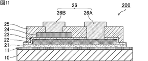
- FIG. 11 is a cross-sectional view schematically showing an example of a capacitor provided with the support substrate of the present invention.
- FIG. 12 is a plan view schematically showing an example of a capacitor provided with the support substrate of the present invention.
- 11 is a cross-sectional view of the capacitor shown in FIG. 12 taken along line XI--XI.
- the capacitor 200 shown in FIGS. 11 and 12 is provided on the semiconductor substrate 10, the charge trap layer 11 having a higher density of crystal defects than the semiconductor substrate 10, and the charge trap layer 11.
- the external electrodes 26 include first external electrodes 26A connected to the first electrode layer 22 and second external electrodes 26B connected to the second electrode layer 24 .
- the first external electrode 26A penetrates the protective layer 25 and the dielectric film 23, and the second external electrode 26B penetrates the protective layer 25.
- the semiconductor substrate 10, the charge trap layer 11 and the insulating layer 21 constitute the supporting substrate of the present invention.
- the configuration of the insulating layer 21 may be the configuration described in the first embodiment of the present invention, or may be the configuration described in the second embodiment.
- the first electrode layer 22 is provided at a position away from the edge of the semiconductor substrate 10 . That is, the edge of the first electrode layer 22 is located inside the edge of the semiconductor substrate 10 .
- the material forming the first electrode layer 22 is not particularly limited, but Cu, Ag, Au, Al, Ni, Cr, Ti, or alloys containing at least one of these metals are preferred.
- the dielectric film 23 is provided so as to cover the first electrode layer 22 except for the opening. It is also provided on the surface of layer 21 .
- the material forming the dielectric film 23 is not particularly limited, but oxides or nitrides such as SiO 2 , SiN, Al 2 O 3 , HfO 2 and Ta 2 O 5 are preferred.
- the second electrode layer 24 is provided facing the first electrode layer 22 with the dielectric film 23 interposed therebetween.
- the material forming the second electrode layer 24 is not particularly limited, but Cu, Ag, Au, Al, Ni, Cr, Ti, or alloys containing at least one of these metals are preferred.
- the protective layer 25 is provided so as to cover the dielectric film 23 and the second electrode layer 24 except for the opening overlapping the second electrode layer 24 . Furthermore, the protective layer 25 is provided with an opening at a position overlapping the opening of the dielectric film 23 (the opening overlapping the first electrode layer 22). The provision of the protective layer 25 protects the capacitor element, particularly the dielectric film 23, from moisture.
- the material forming the protective layer 25 is not particularly limited, but preferably includes resin materials such as polyimide resin and resin in solder resist.
- a moisture-resistant film may be provided between the dielectric film 23 and the protective layer 25 .
- the moisture-resistant film is provided so as to cover the dielectric film 23 and the second electrode layer 24 except for the opening overlapping the second electrode layer 24 and the opening overlapping the first electrode layer 22 .
- moisture-resistant films Materials constituting the moisture-resistant film are not particularly limited, but moisture-resistant materials such as SiO 2 and SiN are preferred.
- the material that constitutes the external electrode 26 is not particularly limited, but Cu, Ni, Ag, Au, Al, or the like is preferable.
- the external electrode 26 may have a single layer structure or a multilayer structure.
- the outermost surface of the external electrode 26 is preferably made of Au or Sn.
- a capacitor having the above structure can be manufactured by a known method described in, for example, International Publication No. 2019/021827 after manufacturing the support substrate of the present invention.
- FIG. 13 is a cross-sectional view schematically showing another example of the capacitor provided with the supporting substrate of the present invention.
- the capacitor 210 shown in FIG. 13 includes a semiconductor substrate 10, a charge trap layer 11 provided on the semiconductor substrate 10 and having a high density of crystal defects with respect to the semiconductor substrate 10, and an insulating layer provided on the charge trap layer 11. 21, a first electrode layer 22 provided on the insulating layer 21, a dielectric film 23 provided on the first electrode layer 22, a second electrode layer 24 provided on the dielectric film 23, A third electrode layer 27 provided on the dielectric film 23 apart from the second electrode layer 24, a protective layer 25 covering the second electrode layer 24 and the third electrode layer 27, and an external electrode penetrating the protective layer 25 26 and.
- the external electrodes 26 include first external electrodes 26A connected to the third electrode layer 27 and second external electrodes 26B connected to the second electrode layer 24 .
- the first external electrode 26A penetrates the protective layer 25, and the second external electrode 26B penetrates the protective layer 25.
- capacitors are formed on the left side, whereas in the configuration of the capacitor 210 shown in FIG. 13, capacitors are formed on the left and right sides.
- the portion where the first external electrode 26A is connected to the first electrode layer 22 in the structure shown in FIG. It's just replacing the provided components. Therefore, the configuration shown in FIG. 13 does not require additional device formation space as compared with the configuration shown in FIG. Therefore, a capacitor with a low capacitance can be manufactured with the same element area.
- Such a structure is effective when a dielectric film having a certain thickness or more cannot be formed.
- FIG. 14 is a cross-sectional view schematically showing an example of a surface acoustic wave device provided with the supporting substrate of the present invention.
- a surface acoustic wave device 300 shown in FIG. a single crystal piezoelectric thin film 31 provided on the insulating layer 21; an IDT (InterDigital Transducer) electrode 32 provided on the single crystal piezoelectric thin film 31; a protective layer 35 covering the IDT electrode 32; and an external electrode 36 penetrating through the protective layer 35 .
- IDT InterDigital Transducer
- the semiconductor substrate 10, the charge trap layer 11 and the insulating layer 21 constitute the support substrate of the present invention.
- the configuration of the insulating layer 21 may be the configuration described in the first embodiment of the present invention, or may be the configuration described in the second embodiment.
- FIG. 15 is a cross-sectional view schematically showing an example of a bulk acoustic wave device provided with the supporting substrate of the present invention.
- Bulk acoustic wave device 400 shown in FIG. 15 is provided on semiconductor substrate 10, on charge trap layer 11 having a high crystal defect density with respect to semiconductor substrate 10, and on charge trap layer 11.
- the external electrodes 46 include first external electrodes 46A connected to the first electrode layer 22 and second external electrodes 46B connected to the second electrode layer 24 .
- the first external electrode 46A penetrates the protective layer 45, and the second external electrode 46B penetrates the protective layer 45.
- a cavity 47 is formed in part of the semiconductor substrate 10 below at least the region where the first electrode layer 42 and the second electrode layer 44 overlap. Therefore, bulk acoustic wave device 400 has a so-called membrane structure.
- the semiconductor substrate 10, the charge trap layer 11 and the insulating layer 21 constitute the support substrate of the present invention.
- the configuration of the insulating layer 21 may be the configuration described in the first embodiment of the present invention, or may be the configuration described in the second embodiment.
- the semiconductor device of the present invention which is an example of the passive electronic component of the present invention, has a high Q characteristic and is therefore suitably used as a capacitor in matching circuits or filter circuits.
- a matching circuit or a filter circuit including the semiconductor device of the present invention is also one aspect of the present invention.
- FIG. 16 is an explanatory diagram showing an example of a matching circuit.
- the semiconductor device of the present invention for the capacitor C of the matching circuit shown in FIG. 16, the power consumption of the entire circuit can be suppressed.
- FIG. 17 is an explanatory diagram showing an example of a filter circuit.
- the semiconductor device of the present invention for the capacitor C1 of the filter circuit shown in FIG. 17, the power consumption of the entire circuit can be suppressed.
- Reference Signs List 10 100 semiconductor substrate 11 charge trap layer 12 inversion region 13 depletion layer 21, 121 insulating layer 21A first insulating layer 21B second insulating layer 22, 42 first electrode layer 23 dielectric film 24, 44 second electrode layer 25, 35, 45 protective layer 26, 36, 46 external electrode 26A, 46A first external electrode 26B, 46B second external electrode 27 third electrode layer 31 single crystal piezoelectric thin film 32 IDT electrode 43 piezoelectric film 47 cavity 122, 123 electrode 200, 210 capacitors (semiconductor devices) 300 surface acoustic wave device (semiconductor device) 400 bulk acoustic wave device (semiconductor device)
Landscapes
- Engineering & Computer Science (AREA)
- Power Engineering (AREA)
- Physics & Mathematics (AREA)
- Acoustics & Sound (AREA)
- Microelectronics & Electronic Packaging (AREA)
- Manufacturing & Machinery (AREA)
- Semiconductor Integrated Circuits (AREA)
Priority Applications (3)
| Application Number | Priority Date | Filing Date | Title |
|---|---|---|---|
| CN202280033513.5A CN117397030A (zh) | 2021-05-10 | 2022-05-09 | 无源电子部件用的支承基板、无源电子部件、半导体装置、匹配电路以及滤波电路 |
| JP2023521006A JP7635834B2 (ja) | 2021-05-10 | 2022-05-09 | 受動電子部品用の支持基板、受動電子部品、半導体装置、マッチング回路及びフィルタ回路 |
| US18/497,020 US20240063224A1 (en) | 2021-05-10 | 2023-10-30 | Support substrate for passive electronic component, passive electronic component, semiconductor device, matching circuit, and filter circuit |
Applications Claiming Priority (2)
| Application Number | Priority Date | Filing Date | Title |
|---|---|---|---|
| JP2021079850 | 2021-05-10 | ||
| JP2021-079850 | 2021-05-10 |
Related Child Applications (1)
| Application Number | Title | Priority Date | Filing Date |
|---|---|---|---|
| US18/497,020 Continuation US20240063224A1 (en) | 2021-05-10 | 2023-10-30 | Support substrate for passive electronic component, passive electronic component, semiconductor device, matching circuit, and filter circuit |
Publications (1)
| Publication Number | Publication Date |
|---|---|
| WO2022239719A1 true WO2022239719A1 (ja) | 2022-11-17 |
Family
ID=84029622
Family Applications (1)
| Application Number | Title | Priority Date | Filing Date |
|---|---|---|---|
| PCT/JP2022/019621 Ceased WO2022239719A1 (ja) | 2021-05-10 | 2022-05-09 | 受動電子部品用の支持基板、受動電子部品、半導体装置、マッチング回路及びフィルタ回路 |
Country Status (4)
| Country | Link |
|---|---|
| US (1) | US20240063224A1 (https=) |
| JP (1) | JP7635834B2 (https=) |
| CN (1) | CN117397030A (https=) |
| WO (1) | WO2022239719A1 (https=) |
Cited By (1)
| Publication number | Priority date | Publication date | Assignee | Title |
|---|---|---|---|---|
| WO2024252872A1 (ja) * | 2023-06-07 | 2024-12-12 | 株式会社村田製作所 | 半導体装置、マッチング回路及びフィルタ回路 |
Citations (4)
| Publication number | Priority date | Publication date | Assignee | Title |
|---|---|---|---|---|
| JP2002530868A (ja) * | 1998-11-13 | 2002-09-17 | テレフオンアクチーボラゲツト エル エム エリクソン(パブル) | ポリシリコンレジスタおよびそれを生産する方法 |
| JP2007258713A (ja) * | 2006-03-17 | 2007-10-04 | Sychip Inc | 集積受動デバイス基板 |
| JP2020170782A (ja) * | 2019-04-03 | 2020-10-15 | 株式会社村田製作所 | キャパシタ |
| JP2020188091A (ja) * | 2019-05-13 | 2020-11-19 | 株式会社村田製作所 | キャパシタ |
-
2022
- 2022-05-09 CN CN202280033513.5A patent/CN117397030A/zh active Pending
- 2022-05-09 WO PCT/JP2022/019621 patent/WO2022239719A1/ja not_active Ceased
- 2022-05-09 JP JP2023521006A patent/JP7635834B2/ja active Active
-
2023
- 2023-10-30 US US18/497,020 patent/US20240063224A1/en active Pending
Patent Citations (4)
| Publication number | Priority date | Publication date | Assignee | Title |
|---|---|---|---|---|
| JP2002530868A (ja) * | 1998-11-13 | 2002-09-17 | テレフオンアクチーボラゲツト エル エム エリクソン(パブル) | ポリシリコンレジスタおよびそれを生産する方法 |
| JP2007258713A (ja) * | 2006-03-17 | 2007-10-04 | Sychip Inc | 集積受動デバイス基板 |
| JP2020170782A (ja) * | 2019-04-03 | 2020-10-15 | 株式会社村田製作所 | キャパシタ |
| JP2020188091A (ja) * | 2019-05-13 | 2020-11-19 | 株式会社村田製作所 | キャパシタ |
Cited By (1)
| Publication number | Priority date | Publication date | Assignee | Title |
|---|---|---|---|---|
| WO2024252872A1 (ja) * | 2023-06-07 | 2024-12-12 | 株式会社村田製作所 | 半導体装置、マッチング回路及びフィルタ回路 |
Also Published As
| Publication number | Publication date |
|---|---|
| US20240063224A1 (en) | 2024-02-22 |
| JP7635834B2 (ja) | 2025-02-26 |
| JPWO2022239719A1 (https=) | 2022-11-17 |
| CN117397030A (zh) | 2024-01-12 |
Similar Documents
| Publication | Publication Date | Title |
|---|---|---|
| JP5842911B2 (ja) | 圧電デバイス、圧電デバイスの製造方法 | |
| US6806553B2 (en) | Tunable thin film capacitor | |
| TWI401745B (zh) | Semiconductor device and manufacturing method thereof | |
| JP3842745B2 (ja) | 半導体装置およびその製造方法 | |
| US9368712B2 (en) | Surface acoustic wave device | |
| JPH0621391A (ja) | 強誘電体コンデンサ及びその形成方法 | |
| KR20110050926A (ko) | 트랜지스터와 그 제조방법 및 트랜지스터를 포함하는 전자소자 | |
| JPWO2002061943A1 (ja) | Sawデバイス及びその製造方法 | |
| JP7635834B2 (ja) | 受動電子部品用の支持基板、受動電子部品、半導体装置、マッチング回路及びフィルタ回路 | |
| JP2009177192A (ja) | 半導体デバイスとゲート誘電体組み合わせ層の形成方法 | |
| JP6040904B2 (ja) | 半導体装置およびその製造方法 | |
| JP2005142629A (ja) | 弾性表面波素子およびその製造方法 | |
| KR100658259B1 (ko) | 반도체장치 및 그 제조방법 | |
| JPH11233760A (ja) | 金属、酸化膜及び炭化珪素半導体からなる積層構造体 | |
| JP3401244B2 (ja) | 電気光学素子 | |
| JP2001094382A (ja) | 弾性表面波装置およびその製造方法 | |
| JP5093946B2 (ja) | 可変容量コンデンサおよび製造方法 | |
| JP4798870B2 (ja) | 可変容量コンデンサ | |
| JPWO2001001190A1 (ja) | 電気光学素子およびその製造方法 | |
| JP2017034454A (ja) | 電子部品及び電子部品の製造方法 | |
| JP2011124745A (ja) | 弾性波デバイスおよびその製造方法 | |
| JPS60734A (ja) | 半導体装置とその製造方法 | |
| JP2002329641A (ja) | 可変容量コンデンサおよび製造方法 | |
| CN118525368A (zh) | 具有用于氢捕获的吸气剂层的集成电路 | |
| JPH05243628A (ja) | ジョセフソン接合素子及びその製造方法 |
Legal Events
| Date | Code | Title | Description |
|---|---|---|---|
| 121 | Ep: the epo has been informed by wipo that ep was designated in this application |
Ref document number: 22807421 Country of ref document: EP Kind code of ref document: A1 |
|
| WWE | Wipo information: entry into national phase |
Ref document number: 202280033513.5 Country of ref document: CN |
|
| WWE | Wipo information: entry into national phase |
Ref document number: 2023521006 Country of ref document: JP |
|
| NENP | Non-entry into the national phase |
Ref country code: DE |
|
| 122 | Ep: pct application non-entry in european phase |
Ref document number: 22807421 Country of ref document: EP Kind code of ref document: A1 |