WO2022239719A1 - 受動電子部品用の支持基板、受動電子部品、半導体装置、マッチング回路及びフィルタ回路 - Google Patents
受動電子部品用の支持基板、受動電子部品、半導体装置、マッチング回路及びフィルタ回路 Download PDFInfo
- Publication number
- WO2022239719A1 WO2022239719A1 PCT/JP2022/019621 JP2022019621W WO2022239719A1 WO 2022239719 A1 WO2022239719 A1 WO 2022239719A1 JP 2022019621 W JP2022019621 W JP 2022019621W WO 2022239719 A1 WO2022239719 A1 WO 2022239719A1
- Authority
- WO
- WIPO (PCT)
- Prior art keywords
- insulating layer
- layer
- support substrate
- type
- charge
- Prior art date
Links
- 239000000758 substrate Substances 0.000 title claims abstract description 147
- 239000004065 semiconductor Substances 0.000 title claims abstract description 79
- 239000013078 crystal Substances 0.000 claims abstract description 19
- 229910052710 silicon Inorganic materials 0.000 claims abstract description 19
- 230000007547 defect Effects 0.000 claims abstract description 13
- 229910052581 Si3N4 Inorganic materials 0.000 claims abstract description 8
- HQVNEWCFYHHQES-UHFFFAOYSA-N silicon nitride Chemical compound N12[Si]34N5[Si]62N3[Si]51N64 HQVNEWCFYHHQES-UHFFFAOYSA-N 0.000 claims abstract description 8
- 239000010410 layer Substances 0.000 claims description 293
- 239000000463 material Substances 0.000 claims description 25
- 239000011241 protective layer Substances 0.000 claims description 24
- 229910021420 polycrystalline silicon Inorganic materials 0.000 claims description 15
- 229910004298 SiO 2 Inorganic materials 0.000 claims description 14
- 239000000470 constituent Substances 0.000 claims description 13
- 238000000034 method Methods 0.000 claims description 12
- 229910021421 monocrystalline silicon Inorganic materials 0.000 claims description 7
- 229910021417 amorphous silicon Inorganic materials 0.000 claims description 6
- 229910052782 aluminium Inorganic materials 0.000 claims description 5
- 230000000149 penetrating effect Effects 0.000 claims description 5
- 150000001875 compounds Chemical class 0.000 claims description 4
- 230000003647 oxidation Effects 0.000 claims 2
- 238000007254 oxidation reaction Methods 0.000 claims 2
- 238000003763 carbonization Methods 0.000 claims 1
- 238000003682 fluorination reaction Methods 0.000 claims 1
- 238000009413 insulation Methods 0.000 abstract 10
- 125000004429 atom Chemical group 0.000 abstract 1
- 125000004433 nitrogen atom Chemical group N* 0.000 abstract 1
- 239000010408 film Substances 0.000 description 40
- 239000003990 capacitor Substances 0.000 description 33
- 238000010586 diagram Methods 0.000 description 14
- 230000000694 effects Effects 0.000 description 8
- 238000010897 surface acoustic wave method Methods 0.000 description 7
- 238000004519 manufacturing process Methods 0.000 description 6
- 238000005229 chemical vapour deposition Methods 0.000 description 5
- 230000003071 parasitic effect Effects 0.000 description 5
- VYPSYNLAJGMNEJ-UHFFFAOYSA-N Silicium dioxide Chemical compound O=[Si]=O VYPSYNLAJGMNEJ-UHFFFAOYSA-N 0.000 description 4
- 230000015572 biosynthetic process Effects 0.000 description 4
- 230000006866 deterioration Effects 0.000 description 4
- 229910052737 gold Inorganic materials 0.000 description 4
- 229910052751 metal Inorganic materials 0.000 description 4
- 239000002184 metal Substances 0.000 description 4
- 238000004544 sputter deposition Methods 0.000 description 4
- 239000010409 thin film Substances 0.000 description 4
- 238000007740 vapor deposition Methods 0.000 description 4
- 238000004833 X-ray photoelectron spectroscopy Methods 0.000 description 3
- 229910052802 copper Inorganic materials 0.000 description 3
- 230000007423 decrease Effects 0.000 description 3
- 229910052759 nickel Inorganic materials 0.000 description 3
- 229910052709 silver Inorganic materials 0.000 description 3
- 229910018072 Al 2 O 3 Inorganic materials 0.000 description 2
- 229910004541 SiN Inorganic materials 0.000 description 2
- -1 SiOC Inorganic materials 0.000 description 2
- 229910020177 SiOF Inorganic materials 0.000 description 2
- 229910045601 alloy Inorganic materials 0.000 description 2
- 239000000956 alloy Substances 0.000 description 2
- 229910052804 chromium Inorganic materials 0.000 description 2
- 229910052681 coesite Inorganic materials 0.000 description 2
- 229910052906 cristobalite Inorganic materials 0.000 description 2
- 239000012212 insulator Substances 0.000 description 2
- 238000005259 measurement Methods 0.000 description 2
- 239000012528 membrane Substances 0.000 description 2
- 150000002739 metals Chemical class 0.000 description 2
- 239000000203 mixture Substances 0.000 description 2
- 239000011347 resin Substances 0.000 description 2
- 229920005989 resin Polymers 0.000 description 2
- 239000000377 silicon dioxide Substances 0.000 description 2
- 235000012239 silicon dioxide Nutrition 0.000 description 2
- 229910052682 stishovite Inorganic materials 0.000 description 2
- 229910052719 titanium Inorganic materials 0.000 description 2
- 229910052905 tridymite Inorganic materials 0.000 description 2
- 229910004140 HfO Inorganic materials 0.000 description 1
- XUIMIQQOPSSXEZ-UHFFFAOYSA-N Silicon Chemical compound [Si] XUIMIQQOPSSXEZ-UHFFFAOYSA-N 0.000 description 1
- 230000032683 aging Effects 0.000 description 1
- PNEYBMLMFCGWSK-UHFFFAOYSA-N aluminium oxide Inorganic materials [O-2].[O-2].[O-2].[Al+3].[Al+3] PNEYBMLMFCGWSK-UHFFFAOYSA-N 0.000 description 1
- 230000005540 biological transmission Effects 0.000 description 1
- 239000002131 composite material Substances 0.000 description 1
- 229910052593 corundum Inorganic materials 0.000 description 1
- 238000002425 crystallisation Methods 0.000 description 1
- 230000008025 crystallization Effects 0.000 description 1
- 230000006378 damage Effects 0.000 description 1
- 150000002500 ions Chemical class 0.000 description 1
- 150000004767 nitrides Chemical class 0.000 description 1
- 238000005498 polishing Methods 0.000 description 1
- 229920001721 polyimide Polymers 0.000 description 1
- 239000009719 polyimide resin Substances 0.000 description 1
- 239000010703 silicon Substances 0.000 description 1
- 239000002356 single layer Substances 0.000 description 1
- 229910000679 solder Inorganic materials 0.000 description 1
- 238000004381 surface treatment Methods 0.000 description 1
- 229910052718 tin Inorganic materials 0.000 description 1
- 229910001845 yogo sapphire Inorganic materials 0.000 description 1
Images


Classifications
-
- H—ELECTRICITY
- H01—ELECTRIC ELEMENTS
- H01L—SEMICONDUCTOR DEVICES NOT COVERED BY CLASS H10
- H01L27/00—Devices consisting of a plurality of semiconductor or other solid-state components formed in or on a common substrate
- H01L27/02—Devices consisting of a plurality of semiconductor or other solid-state components formed in or on a common substrate including semiconductor components specially adapted for rectifying, oscillating, amplifying or switching and having at least one potential-jump barrier or surface barrier; including integrated passive circuit elements with at least one potential-jump barrier or surface barrier
- H01L27/12—Devices consisting of a plurality of semiconductor or other solid-state components formed in or on a common substrate including semiconductor components specially adapted for rectifying, oscillating, amplifying or switching and having at least one potential-jump barrier or surface barrier; including integrated passive circuit elements with at least one potential-jump barrier or surface barrier the substrate being other than a semiconductor body, e.g. an insulating body
- H01L27/1203—Devices consisting of a plurality of semiconductor or other solid-state components formed in or on a common substrate including semiconductor components specially adapted for rectifying, oscillating, amplifying or switching and having at least one potential-jump barrier or surface barrier; including integrated passive circuit elements with at least one potential-jump barrier or surface barrier the substrate being other than a semiconductor body, e.g. an insulating body the substrate comprising an insulating body on a semiconductor body, e.g. SOI
-
- H—ELECTRICITY
- H01—ELECTRIC ELEMENTS
- H01G—CAPACITORS; CAPACITORS, RECTIFIERS, DETECTORS, SWITCHING DEVICES OR LIGHT-SENSITIVE DEVICES, OF THE ELECTROLYTIC TYPE
- H01G4/00—Fixed capacitors; Processes of their manufacture
- H01G4/30—Stacked capacitors
-
- H—ELECTRICITY
- H01—ELECTRIC ELEMENTS
- H01G—CAPACITORS; CAPACITORS, RECTIFIERS, DETECTORS, SWITCHING DEVICES OR LIGHT-SENSITIVE DEVICES, OF THE ELECTROLYTIC TYPE
- H01G4/00—Fixed capacitors; Processes of their manufacture
- H01G4/33—Thin- or thick-film capacitors
-
- H—ELECTRICITY
- H01—ELECTRIC ELEMENTS
- H01L—SEMICONDUCTOR DEVICES NOT COVERED BY CLASS H10
- H01L21/00—Processes or apparatus adapted for the manufacture or treatment of semiconductor or solid state devices or of parts thereof
- H01L21/70—Manufacture or treatment of devices consisting of a plurality of solid state components formed in or on a common substrate or of parts thereof; Manufacture of integrated circuit devices or of parts thereof
- H01L21/77—Manufacture or treatment of devices consisting of a plurality of solid state components or integrated circuits formed in, or on, a common substrate
- H01L21/78—Manufacture or treatment of devices consisting of a plurality of solid state components or integrated circuits formed in, or on, a common substrate with subsequent division of the substrate into plural individual devices
- H01L21/82—Manufacture or treatment of devices consisting of a plurality of solid state components or integrated circuits formed in, or on, a common substrate with subsequent division of the substrate into plural individual devices to produce devices, e.g. integrated circuits, each consisting of a plurality of components
- H01L21/822—Manufacture or treatment of devices consisting of a plurality of solid state components or integrated circuits formed in, or on, a common substrate with subsequent division of the substrate into plural individual devices to produce devices, e.g. integrated circuits, each consisting of a plurality of components the substrate being a semiconductor, using silicon technology
-
- H—ELECTRICITY
- H01—ELECTRIC ELEMENTS
- H01L—SEMICONDUCTOR DEVICES NOT COVERED BY CLASS H10
- H01L27/00—Devices consisting of a plurality of semiconductor or other solid-state components formed in or on a common substrate
- H01L27/02—Devices consisting of a plurality of semiconductor or other solid-state components formed in or on a common substrate including semiconductor components specially adapted for rectifying, oscillating, amplifying or switching and having at least one potential-jump barrier or surface barrier; including integrated passive circuit elements with at least one potential-jump barrier or surface barrier
- H01L27/04—Devices consisting of a plurality of semiconductor or other solid-state components formed in or on a common substrate including semiconductor components specially adapted for rectifying, oscillating, amplifying or switching and having at least one potential-jump barrier or surface barrier; including integrated passive circuit elements with at least one potential-jump barrier or surface barrier the substrate being a semiconductor body
-
- H—ELECTRICITY
- H01—ELECTRIC ELEMENTS
- H01L—SEMICONDUCTOR DEVICES NOT COVERED BY CLASS H10
- H01L28/00—Passive two-terminal components without a potential-jump or surface barrier for integrated circuits; Details thereof; Multistep manufacturing processes therefor
- H01L28/40—Capacitors
-
- H—ELECTRICITY
- H01—ELECTRIC ELEMENTS
- H01P—WAVEGUIDES; RESONATORS, LINES, OR OTHER DEVICES OF THE WAVEGUIDE TYPE
- H01P1/00—Auxiliary devices
- H01P1/20—Frequency-selective devices, e.g. filters
-
- H—ELECTRICITY
- H03—ELECTRONIC CIRCUITRY
- H03H—IMPEDANCE NETWORKS, e.g. RESONANT CIRCUITS; RESONATORS
- H03H7/00—Multiple-port networks comprising only passive electrical elements as network components
- H03H7/01—Frequency selective two-port networks
- H03H7/0115—Frequency selective two-port networks comprising only inductors and capacitors
-
- H—ELECTRICITY
- H03—ELECTRONIC CIRCUITRY
- H03H—IMPEDANCE NETWORKS, e.g. RESONANT CIRCUITS; RESONATORS
- H03H7/00—Multiple-port networks comprising only passive electrical elements as network components
- H03H7/38—Impedance-matching networks
-
- H—ELECTRICITY
- H03—ELECTRONIC CIRCUITRY
- H03H—IMPEDANCE NETWORKS, e.g. RESONANT CIRCUITS; RESONATORS
- H03H7/00—Multiple-port networks comprising only passive electrical elements as network components
- H03H7/46—Networks for connecting several sources or loads, working on different frequencies or frequency bands, to a common load or source
-
- H—ELECTRICITY
- H03—ELECTRONIC CIRCUITRY
- H03H—IMPEDANCE NETWORKS, e.g. RESONANT CIRCUITS; RESONATORS
- H03H9/00—Networks comprising electromechanical or electro-acoustic devices; Electromechanical resonators
- H03H9/02—Details
- H03H9/02007—Details of bulk acoustic wave devices
- H03H9/02086—Means for compensation or elimination of undesirable effects
- H03H9/02125—Means for compensation or elimination of undesirable effects of parasitic elements
-
- H—ELECTRICITY
- H03—ELECTRONIC CIRCUITRY
- H03H—IMPEDANCE NETWORKS, e.g. RESONANT CIRCUITS; RESONATORS
- H03H9/00—Networks comprising electromechanical or electro-acoustic devices; Electromechanical resonators
- H03H9/02—Details
- H03H9/02535—Details of surface acoustic wave devices
- H03H9/02818—Means for compensation or elimination of undesirable effects
- H03H9/02952—Means for compensation or elimination of undesirable effects of parasitic capacitance
-
- H—ELECTRICITY
- H03—ELECTRONIC CIRCUITRY
- H03H—IMPEDANCE NETWORKS, e.g. RESONANT CIRCUITS; RESONATORS
- H03H9/00—Networks comprising electromechanical or electro-acoustic devices; Electromechanical resonators
- H03H9/15—Constructional features of resonators consisting of piezoelectric or electrostrictive material
- H03H9/17—Constructional features of resonators consisting of piezoelectric or electrostrictive material having a single resonator
- H03H9/171—Constructional features of resonators consisting of piezoelectric or electrostrictive material having a single resonator implemented with thin-film techniques, i.e. of the film bulk acoustic resonator [FBAR] type
- H03H9/172—Means for mounting on a substrate, i.e. means constituting the material interface confining the waves to a volume
- H03H9/173—Air-gaps
-
- H—ELECTRICITY
- H03—ELECTRONIC CIRCUITRY
- H03H—IMPEDANCE NETWORKS, e.g. RESONANT CIRCUITS; RESONATORS
- H03H9/00—Networks comprising electromechanical or electro-acoustic devices; Electromechanical resonators
- H03H9/25—Constructional features of resonators using surface acoustic waves
Definitions
- the present invention relates to a support substrate for passive electronic components. Furthermore, the present invention relates to a passive electronic component and a semiconductor device comprising the supporting substrate, and a matching circuit and a filter circuit comprising the semiconductor device.
- a MIM (Metal Insulator Metal) capacitor for example, is known as a typical capacitor element used in a semiconductor integrated circuit.
- a MIM capacitor is a capacitor having a parallel plate type structure in which an insulator is sandwiched between a lower electrode and an upper electrode.
- Patent Document 1 discloses a substrate comprising a planar silicon wafer, a planar layer of polycrystalline silicon on the wafer, and an insulating layer on the polycrystalline silicon layer. disclosed.
- a polycrystalline silicon layer is formed between a high-resistance single-crystal silicon substrate and an insulating layer made of SiO 2 or the like, so that the single-crystal silicon substrate and the insulating layer are separated. suppresses the formation of a low-resistance layer at the interface with As a result, deterioration of the Q characteristics of passive electronic components such as MIM capacitors formed on the supporting substrate, more specifically, deterioration of the Q characteristics due to parasitic capacitance in a high frequency region can be reduced.
- FIG. 1 is a schematic diagram showing an example of a conventional support substrate.
- + surrounded by squares represents a positive fixed charge
- - surrounded by a circle represents a negative mobile charge (electron)
- + surrounded by a circle represents a positive mobile charge.
- a support substrate 1a shown in FIG. 1 is provided on a semiconductor substrate 10, which is a p-type single crystal Si substrate, on the semiconductor substrate 10, and on a charge trap layer 11 made of polycrystalline Si and on the charge trap layer 11. , and an insulating layer 21 made of SiO 2 . If the insulating layer 21 consists of SiO 2 , the fixed charge inside the insulating layer 21 is positive. As shown in FIG. 1 , accumulated charges (here, electrons) attracted to fixed charges in the insulating layer 21 are trapped in the charge trap layer 11 .
- Patent Document 1 discloses an oxide such as SiO 2 as a constituent material of the insulating layer 21.
- SiO 2 As a constituent material of the insulating layer 21.
- polycrystalline oxide is used.
- a large amount of electrons are generated in the charge trap layer 11 made of Si. Therefore, if the density of charge trapping sites (crystal defects) in the charge trapping layer 11 is insufficient, some of the generated electrons may not be trapped.
- the density of charge trapping sites (crystal defects) also decreases due to the progress of crystallization of polycrystalline Si due to heat load during the device fabrication process, aging, etc., so there is a risk that the generated electrons may not be able to be trapped. . In that case, deterioration of characteristics due to parasitic capacitance occurs.
- the present invention has been made to solve the above problems, and an object of the present invention is to provide a support substrate for passive electronic components that can reduce mobile charges generated in the charge trapping layer.
- a further object of the present invention is to provide a passive electronic component and a semiconductor device comprising the supporting substrate, and a matching circuit and a filter circuit comprising the semiconductor device.
- a support substrate for a passive electronic component comprises a semiconductor substrate, a charge trap layer provided on the semiconductor substrate and having a high density of crystal defects with respect to the semiconductor substrate, and a charge trap layer provided on the charge trap layer. and an insulating layer.
- the insulating layer is made of silicon nitride, and the atomic concentration ratio of N to the total amount of Si and N contained in the insulating layer is 45 atom % or less.
- the insulating layer includes a first insulating layer provided on the charge trapping layer and a second insulating layer provided on the first insulating layer, and the first insulating layer and the second insulating layer have opposite polarities of internal fixed charges, and the thickness of the first insulating layer is 0.5 nm or more and 3 nm or less.
- the passive electronic component of the present invention comprises the support substrate of the present invention.
- a semiconductor device of the present invention comprises a supporting substrate of the present invention, a first electrode layer provided on the supporting substrate, a dielectric film provided on the first electrode layer, and a dielectric film provided on the dielectric film. a second electrode layer, a protective layer covering the first electrode layer and the second electrode layer, and an external electrode penetrating the protective layer.
- the matching circuit of the present invention includes the semiconductor device of the present invention.
- a filter circuit of the present invention includes the semiconductor device of the present invention.
- a support substrate for passive electronic components that can reduce mobile charges generated in the charge trap layer. Furthermore, according to the present invention, it is possible to provide a passive electronic component and a semiconductor device comprising the supporting substrate, and a matching circuit and a filter circuit comprising the semiconductor device.
- FIG. 1 is a schematic diagram showing an example of a conventional support substrate.
- FIG. 2 is a schematic diagram showing an example of the support substrate according to the first embodiment of the present invention.
- FIG. 3 is a schematic diagram showing another example of the support substrate according to the first embodiment of the present invention.
- FIG. 4 is a graph showing the relationship between the atomic concentration ratio of N with respect to the total amount of Si and N contained in the insulating layer and the fixed charge density.
- 5A to 5D are schematic diagrams showing the state of mobile charge when the fixed charge inside the insulating layer is positive.
- FIG. 6 is a top view for explaining a method of measuring fixed charges.
- FIG. 7 is a cross-sectional view for explaining a method of measuring fixed charges.
- FIG. 8 is a graph showing an example of a CV curve.
- FIG. 9 is a schematic diagram showing an example of a support substrate according to the second embodiment of the invention.
- FIG. 10 is a graph showing the relationship between the film thickness of SiO 2 and the fixed charge density in a two-layer insulating layer comprising a first insulating layer made of SiO 2 and a second insulating layer made of SiN.
- FIG. 11 is a cross-sectional view schematically showing an example of a capacitor provided with the support substrate of the present invention.
- FIG. 12 is a plan view schematically showing an example of a capacitor provided with the support substrate of the present invention.
- FIG. 13 is a cross-sectional view schematically showing another example of the capacitor provided with the supporting substrate of the present invention.
- FIG. 14 is a cross-sectional view schematically showing an example of a surface acoustic wave device provided with the supporting substrate of the present invention.
- FIG. 15 is a cross-sectional view schematically showing an example of a bulk acoustic wave device provided with the supporting substrate of the present invention.
- FIG. 16 is an explanatory diagram of an example of a matching circuit.
- FIG. 17 is an explanatory diagram of an example of a filter circuit.
- support substrate for passive electronic components may be abbreviated as “support substrate”.
- support substrate for passive electronic components
- present invention is not limited to the following configurations, and can be appropriately modified and applied without changing the gist of the present invention.
- a combination of two or more of the individual preferred configurations of the present invention described below is also the present invention.
- a support substrate according to the first embodiment of the present invention includes a semiconductor substrate, a charge trap layer provided on the semiconductor substrate and having a high density of crystal defects with respect to the semiconductor substrate, and a charge trap layer provided on the charge trap layer. and an insulating layer.
- the insulating layer is made of silicon nitride, and the atomic concentration ratio of N to the total amount of Si and N contained in the insulating layer is 45 atom % or less.
- FIG. 2 is a schematic diagram showing an example of the support substrate according to the first embodiment of the present invention.
- FIG. 3 is a schematic diagram showing another example of the support substrate according to the first embodiment of the present invention.
- ⁇ surrounded by ⁇ is a negative fixed charge
- + surrounded by ⁇ is a positive fixed charge
- ⁇ surrounded by ⁇ is a negative mobile charge (electron)
- the + represents a positive mobile charge.
- the support substrate 1 shown in FIG. 2 includes a semiconductor substrate 10 , a charge trap layer 11 provided on the semiconductor substrate 10 and having a high density of crystal defects with respect to the semiconductor substrate 10 , and an insulating layer 11 provided on the charge trap layer 11 . a layer 21; In the support substrate 1 shown in FIG. 2, the fixed charge inside the insulating layer 21 is positive.
- a support substrate 1A shown in FIG. a layer 21; In the supporting substrate 1A shown in FIG. 3, the fixed charge inside the insulating layer 21 is negative.
- fixed charges inside the insulating layer are adjusted so as to reduce mobile charges generated at the interface between the insulating layer and the charge trap layer. Specifically, by forming an insulating layer with reduced internal fixed charges at the interface with the charge trap layer, mobile charges generated inside the charge trap layer can be reduced.
- the effect of parasitic capacitance from the semiconductor substrate can be further reduced by further increasing the resistivity of the charge trapping layer.
- the required performance of the charge trap layer can be lowered. For example, since the heat-resistant temperature and heat-resistant time of the constituent material of the charge trap layer can be extended, restrictions on the manufacturing method or temperature in the device manufacturing process can be reduced.
- the semiconductor substrate is preferably a high resistance Si substrate, more preferably a single crystal Si substrate.
- the resistivity of the semiconductor substrate is preferably 3 k ⁇ cm or more, more preferably 5 k ⁇ cm or more.
- a Si substrate such as a single-crystal Si substrate may be either p-type or n-type, but the p-type is preferable because the high-resistance n-type Si substrate is fragile and difficult to control the resistance.
- the charge trap layer which has a high density of crystal defects with respect to the semiconductor substrate, traps mobile charges generated between itself and the insulating layer.
- the constituent material of the charge trapping layer is preferably a high resistance semiconductor material such as polycrystalline Si or amorphous Si having a charge trapping site.
- the resistivity of the charge trapping layer is preferably equal to or higher than that of the semiconductor substrate.
- the region in which mobile charges exist in the charge trap layer has the highest density near the interface with the insulating layer, decreases with distance from the insulating layer, but extends to a depth of about 1 to 2 ⁇ m. Therefore, the thickness of the charge trap layer is preferably 1 ⁇ m or more, more preferably 2 ⁇ m or more. On the other hand, the thickness of the charge trap layer is, for example, 10 ⁇ m or less.
- the charge trap layer include a polycrystalline Si film, an amorphous Si film, a crystal destruction layer obtained by implanting rare gas ions into the Si surface, and a crystal distortion layer obtained by grinding or polishing.
- the constituent material of the charge trap layer is preferably polycrystalline Si or amorphous Si because of the thermal stability of the film structure and the ease of controlling the thickness.
- a polycrystalline Si film or an amorphous Si film can be formed using vapor deposition methods such as chemical vapor deposition (CVD) and sputtering, respectively.
- the insulating layer has as little fixed charge as possible therein.
- the commonly used insulating layer made of SiO2 has a positive fixed charge, but since it is difficult to control the Si/O composition ratio and bond, the amount of fixed charge can be adjusted as a stable film. It is not easy to turn or reverse. Therefore, a thermal oxide film has been used, which can most stably reduce the fixed charges. However, since even the thermal oxide film has a large amount of fixed charge, improvement of the charge trapping layer has been investigated.
- the Si/N composition ratio of the insulating layer made of silicon nitride is adjusted to change from N-rich to Si-rich, thereby reducing the generated fixed charges from negative to negative. It can be controlled up to positive.
- FIG. 4 is a graph showing the relationship between the atomic concentration ratio of N to the total amount of Si and N contained in the insulating layer and the fixed charge density.
- Si 3 N 4 which is a stoichiometric silicon nitride
- the atomic concentration ratio of N to the total amount of Si and N is 57.2 atom %.
- An insulating layer made of Si 3 N 4 has a negative fixed charge. From FIG. 4, the fixed charge can be reduced by setting the atomic concentration ratio of N to 46 atom % or less with respect to the total amount of Si and N contained in the insulating layer. In particular, when the atomic concentration ratio of N to the total amount of Si and N contained in the insulating layer is 45 atom % or less, the fixed charge can be greatly reduced.
- the magnitude of the fixed charge inside the insulating layer can be made very small negative.
- the magnitude of the fixed charges inside the insulating layer can be made very small and positive. In order to make it positive more stably, it is preferably 43 atom % or less.
- FIG. 2 above shows the state of mobile charges generated at the interface with the charge trapping layer when the fixed charge inside the insulating layer is positive, and FIG. The state of mobile charge generated at the interface with the charge trapping layer is shown when the charge is negative.
- the lower limit of the atomic concentration ratio of N to the total amount of Si and N contained in the insulating layer is not particularly limited. There is therefore, the atomic concentration ratio of N to the total amount of Si and N contained in the insulating layer is preferably 38 atom % or more.
- the atomic concentration ratio of N to the total amount of Si and N contained in the insulating layer can be calculated by analyzing the constituent elements of the insulating layer by X-ray photoelectron spectroscopy (XPS).
- XPS X-ray photoelectron spectroscopy
- Measurement device Quantes manufactured by ULVAC-Phi Measurement area: 100 ⁇ m ⁇ Measurement depth: 100nm
- the insulating layer made of silicon nitride can be formed using vapor deposition methods such as CVD and sputtering.
- the thickness of the insulating layer made of silicon nitride is preferably 10 nm or more and 2000 nm or less.
- 5A to 5D are schematic diagrams showing the state of mobile charges when the fixed charges inside the insulating layer are positive.
- the effect of suppressing mobile charges differs depending on the combination of the conductivity type of the semiconductor substrate 10, the conductivity type of the charge trapping layer 11, and the polarity of the fixed charges inside the insulating layer 21.
- the fixed charge inside the insulating layer 21 is positive, as shown in FIG. Since the inversion region 12 and the depletion layer 13 (see FIGS. 5A to 5C) are not formed inside the charge trapping layer 11 and the moving charge region is 5 ⁇ m or more, the charge trapping layer 11 cannot contain all the moving charges. As a result, part of the mobile charge leaks to the semiconductor substrate 10, creating a low-resistance region.
- the combination of the conductivity type of the semiconductor substrate 10 and the conductivity type of the charge trap layer 11 is p type-p type, p-type-n-type or n-type-p-type.
- the charge trapping layer 11 has an inverted charge inside the charge trapping layer 11 . Since the region 12 and the depletion layer 13 (see FIGS. 5A to 5C) are not formed and the region of mobile charges is 5 ⁇ m or more, the mobile charges cannot be contained in the charge trap layer 11 . As a result, part of the mobile charge leaks to the semiconductor substrate 10, creating a low-resistance region.
- the combination of the conductivity type of the semiconductor substrate 10 and the conductivity type of the charge trap layer 11 is n type-n type, n type-p type, or p type-n A mold is preferred.
- the hole mobility is smaller than the electron mobility.
- the degree of decrease in resistance is small, so the charges generated at the interface between the insulating layer 21 and the charge trap layer 11 are preferably holes.
- FIG. 6 is a top view for explaining the method of measuring fixed charges.
- FIG. 7 is a cross-sectional view for explaining a method of measuring fixed charges.
- an insulating layer 121 is formed on one main surface of a semiconductor substrate 100, which is a Si substrate having a resistivity of 1 ⁇ cm or more and 10 ⁇ cm or less, and an electrode 122 is formed on the insulating layer 121. . Furthermore, an electrode 123 is formed on the other main surface of the semiconductor substrate 10 . After that, as shown in FIG. 7, the CV characteristics between the electrodes 122 and 123 are evaluated.
- FIG. 8 is a graph showing an example of a CV curve.
- the total amount of fixed charges can be obtained. can be calculated.
- the shift from the ideal curve S0 is to the left, the polarity of the fixed charge is positive, and when it is to the right, the polarity of the fixed charge is negative.
- the insulating layer includes a first insulating layer provided on the charge trapping layer and a second insulating layer provided on the first insulating layer, wherein the first insulating layer and The polarity of the internal fixed charge is opposite in the second insulating layer, and the thickness of the first insulating layer is 0.5 nm or more and 3 nm or less.
- FIG. 9 is a schematic diagram showing an example of a support substrate according to the second embodiment of the present invention.
- - surrounded by squares represents negative fixed charges
- + surrounded by squares represents positive fixed charges
- - surrounded by circles represents negative mobile charges (electrons).
- the support substrate 2 shown in FIG. 9 includes a semiconductor substrate 10 , a charge trap layer 11 provided on the semiconductor substrate 10 and having a high density of crystal defects with respect to the semiconductor substrate 10 , and an insulating layer 11 provided on the charge trap layer 11 .
- the insulating layer 21 includes a first insulating layer 21A provided on the charge trap layer 11 and a second insulating layer 21B provided on the first insulating layer 21A.
- the fixed charges inside the first insulating layer 21A are positive, and the fixed charges inside the second insulating layer 21B are negative. That is, the polarities of internal fixed charges are opposite between the first insulating layer 21A and the second insulating layer 21B.
- the insulating layer has a multi-layered structure so as to reduce the mobile charge generated at the interface between the insulating layer and the charge trapping layer, and the apparent fixed charge of the insulating layer is reduced. is made smaller.
- the first insulating layer in contact with the charge trapping layer is made very thin, and the polarity of the fixed charges inside the second insulating layer contacting thereon is opposite to the polarity of the fixed charges inside the first insulating layer.
- the effect of parasitic capacitance from the semiconductor substrate can be further reduced by further increasing the resistivity of the charge trapping layer.
- the required performance of the charge trap layer can be lowered. For example, since the heat-resistant temperature and heat-resistant time of the constituent material of the charge trap layer can be extended, restrictions on the manufacturing method or temperature in the device manufacturing process can be reduced. • Process margins are increased because the magnitude of the mobile charge generated can be precisely controlled.
- the configuration other than the insulating layer is the same as that of the support substrate according to the first embodiment of the present invention.
- FIG. 10 is a graph showing the relationship between the film thickness of SiO 2 and the fixed charge density in a two-layer insulating layer comprising a first insulating layer made of SiO 2 and a second insulating layer made of SiN.
- FIG. 10 shows the composite fixed charge density of the insulating layer with respect to the interface with the charge trapping layer made of polycrystalline Si (total fixed charge density of the two layers).
- the apparent fixed charge of the insulating layer which affects the interface between the charge trapping layer and the first insulating layer, has a relationship with the thickness of the first insulating layer as shown in FIG. From FIG. 10, the apparent fixed charges can be greatly reduced by setting the thickness of the first insulating layer to 0.5 nm or more and 3 nm or less. Therefore, the thickness of the first insulating layer is 0.5 nm or more and 3 nm or less, preferably 0.5 nm or more and 1.5 nm or less. The appropriate thickness of the first insulating layer varies depending on the magnitude of the fixed charges in the second insulating layer.
- the constituent material of the first insulating layer is a compound containing Si and at least one selected from the group consisting of O, N, F and C, or a compound containing Al and O. is preferred, for example SiO 2 , SiN, SiOF, SiOC or Al 2 O 3 .
- SiO2 has a positive fixed charge and SiOF, SiOC , Al2O3 has a negative fixed charge.
- SiN can have positive or negative fixed charges depending on the formation conditions.
- These materials are thermally oxidized, oxidized by plasma, nitrided by plasma, fluorinated by plasma, carbonized by plasma, and formed by film formation methods (CVD, sputtering, etc.) of polycrystalline Si constituting the charge trap layer. , ALD, vapor deposition, etc.).
- CVD chemical vapor deposition
- the constituent material of the second insulating layer may be any material having a fixed charge opposite in polarity to that of the first insulating layer, and is preferably SiN or SiO 2 , for example.
- the thickness of the second insulating layer is preferably 3 nm or more. Since the effect is constant if the thickness of the second insulating layer is 3 nm or more, the thickness of the second insulating layer is preferably 2000 nm or less, for example.
- the second insulating layer can be formed using vapor deposition methods such as CVD and sputtering.
- each layer such as the first insulating layer and the second insulating layer, can be obtained from the average value of ten arbitrary thicknesses measured from a cross section observed using a transmission electron microscope (TEM).
- TEM transmission electron microscope
- the support substrate of the present invention As, for example, a support substrate for a low-capacity capacitor for high frequency applications, it is possible to suppress deterioration in Q characteristics due to parasitic capacitance with a semiconductor substrate in a high frequency band.
- a support substrate for passive electronic components such as a surface acoustic wave device with a single crystal piezoelectric thin film and a membrane type bulk acoustic wave device (FBAR) used in a high frequency band, it can be used in the same way as a capacitor. effect can be obtained.
- FBAR membrane type bulk acoustic wave device
- Passive electronic components include, for example, capacitors, surface acoustic wave devices, bulk acoustic wave devices, and the like.
- a semiconductor device including the supporting substrate of the present invention is also one aspect of the present invention.
- a semiconductor device may be a passive electronic component such as a capacitor itself, or may be a device including a passive electronic component such as a capacitor.
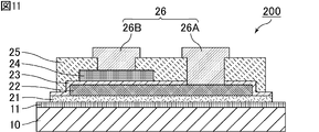
- FIG. 11 is a cross-sectional view schematically showing an example of a capacitor provided with the support substrate of the present invention.
- FIG. 12 is a plan view schematically showing an example of a capacitor provided with the support substrate of the present invention.
- 11 is a cross-sectional view of the capacitor shown in FIG. 12 taken along line XI--XI.
- the capacitor 200 shown in FIGS. 11 and 12 is provided on the semiconductor substrate 10, the charge trap layer 11 having a higher density of crystal defects than the semiconductor substrate 10, and the charge trap layer 11.
- the external electrodes 26 include first external electrodes 26A connected to the first electrode layer 22 and second external electrodes 26B connected to the second electrode layer 24 .
- the first external electrode 26A penetrates the protective layer 25 and the dielectric film 23, and the second external electrode 26B penetrates the protective layer 25.
- the semiconductor substrate 10, the charge trap layer 11 and the insulating layer 21 constitute the supporting substrate of the present invention.
- the configuration of the insulating layer 21 may be the configuration described in the first embodiment of the present invention, or may be the configuration described in the second embodiment.
- the first electrode layer 22 is provided at a position away from the edge of the semiconductor substrate 10 . That is, the edge of the first electrode layer 22 is located inside the edge of the semiconductor substrate 10 .
- the material forming the first electrode layer 22 is not particularly limited, but Cu, Ag, Au, Al, Ni, Cr, Ti, or alloys containing at least one of these metals are preferred.
- the dielectric film 23 is provided so as to cover the first electrode layer 22 except for the opening. It is also provided on the surface of layer 21 .
- the material forming the dielectric film 23 is not particularly limited, but oxides or nitrides such as SiO 2 , SiN, Al 2 O 3 , HfO 2 and Ta 2 O 5 are preferred.
- the second electrode layer 24 is provided facing the first electrode layer 22 with the dielectric film 23 interposed therebetween.
- the material forming the second electrode layer 24 is not particularly limited, but Cu, Ag, Au, Al, Ni, Cr, Ti, or alloys containing at least one of these metals are preferred.
- the protective layer 25 is provided so as to cover the dielectric film 23 and the second electrode layer 24 except for the opening overlapping the second electrode layer 24 . Furthermore, the protective layer 25 is provided with an opening at a position overlapping the opening of the dielectric film 23 (the opening overlapping the first electrode layer 22). The provision of the protective layer 25 protects the capacitor element, particularly the dielectric film 23, from moisture.
- the material forming the protective layer 25 is not particularly limited, but preferably includes resin materials such as polyimide resin and resin in solder resist.
- a moisture-resistant film may be provided between the dielectric film 23 and the protective layer 25 .
- the moisture-resistant film is provided so as to cover the dielectric film 23 and the second electrode layer 24 except for the opening overlapping the second electrode layer 24 and the opening overlapping the first electrode layer 22 .
- moisture-resistant films Materials constituting the moisture-resistant film are not particularly limited, but moisture-resistant materials such as SiO 2 and SiN are preferred.
- the material that constitutes the external electrode 26 is not particularly limited, but Cu, Ni, Ag, Au, Al, or the like is preferable.
- the external electrode 26 may have a single layer structure or a multilayer structure.
- the outermost surface of the external electrode 26 is preferably made of Au or Sn.
- a capacitor having the above structure can be manufactured by a known method described in, for example, International Publication No. 2019/021827 after manufacturing the support substrate of the present invention.
- FIG. 13 is a cross-sectional view schematically showing another example of the capacitor provided with the supporting substrate of the present invention.
- the capacitor 210 shown in FIG. 13 includes a semiconductor substrate 10, a charge trap layer 11 provided on the semiconductor substrate 10 and having a high density of crystal defects with respect to the semiconductor substrate 10, and an insulating layer provided on the charge trap layer 11. 21, a first electrode layer 22 provided on the insulating layer 21, a dielectric film 23 provided on the first electrode layer 22, a second electrode layer 24 provided on the dielectric film 23, A third electrode layer 27 provided on the dielectric film 23 apart from the second electrode layer 24, a protective layer 25 covering the second electrode layer 24 and the third electrode layer 27, and an external electrode penetrating the protective layer 25 26 and.
- the external electrodes 26 include first external electrodes 26A connected to the third electrode layer 27 and second external electrodes 26B connected to the second electrode layer 24 .
- the first external electrode 26A penetrates the protective layer 25, and the second external electrode 26B penetrates the protective layer 25.
- capacitors are formed on the left side, whereas in the configuration of the capacitor 210 shown in FIG. 13, capacitors are formed on the left and right sides.
- the portion where the first external electrode 26A is connected to the first electrode layer 22 in the structure shown in FIG. It's just replacing the provided components. Therefore, the configuration shown in FIG. 13 does not require additional device formation space as compared with the configuration shown in FIG. Therefore, a capacitor with a low capacitance can be manufactured with the same element area.
- Such a structure is effective when a dielectric film having a certain thickness or more cannot be formed.
- FIG. 14 is a cross-sectional view schematically showing an example of a surface acoustic wave device provided with the supporting substrate of the present invention.
- a surface acoustic wave device 300 shown in FIG. a single crystal piezoelectric thin film 31 provided on the insulating layer 21; an IDT (InterDigital Transducer) electrode 32 provided on the single crystal piezoelectric thin film 31; a protective layer 35 covering the IDT electrode 32; and an external electrode 36 penetrating through the protective layer 35 .
- IDT InterDigital Transducer
- the semiconductor substrate 10, the charge trap layer 11 and the insulating layer 21 constitute the support substrate of the present invention.
- the configuration of the insulating layer 21 may be the configuration described in the first embodiment of the present invention, or may be the configuration described in the second embodiment.
- FIG. 15 is a cross-sectional view schematically showing an example of a bulk acoustic wave device provided with the supporting substrate of the present invention.
- Bulk acoustic wave device 400 shown in FIG. 15 is provided on semiconductor substrate 10, on charge trap layer 11 having a high crystal defect density with respect to semiconductor substrate 10, and on charge trap layer 11.
- the external electrodes 46 include first external electrodes 46A connected to the first electrode layer 22 and second external electrodes 46B connected to the second electrode layer 24 .
- the first external electrode 46A penetrates the protective layer 45, and the second external electrode 46B penetrates the protective layer 45.
- a cavity 47 is formed in part of the semiconductor substrate 10 below at least the region where the first electrode layer 42 and the second electrode layer 44 overlap. Therefore, bulk acoustic wave device 400 has a so-called membrane structure.
- the semiconductor substrate 10, the charge trap layer 11 and the insulating layer 21 constitute the support substrate of the present invention.
- the configuration of the insulating layer 21 may be the configuration described in the first embodiment of the present invention, or may be the configuration described in the second embodiment.
- the semiconductor device of the present invention which is an example of the passive electronic component of the present invention, has a high Q characteristic and is therefore suitably used as a capacitor in matching circuits or filter circuits.
- a matching circuit or a filter circuit including the semiconductor device of the present invention is also one aspect of the present invention.
- FIG. 16 is an explanatory diagram showing an example of a matching circuit.
- the semiconductor device of the present invention for the capacitor C of the matching circuit shown in FIG. 16, the power consumption of the entire circuit can be suppressed.
- FIG. 17 is an explanatory diagram showing an example of a filter circuit.
- the semiconductor device of the present invention for the capacitor C1 of the filter circuit shown in FIG. 17, the power consumption of the entire circuit can be suppressed.
- Reference Signs List 10 100 semiconductor substrate 11 charge trap layer 12 inversion region 13 depletion layer 21, 121 insulating layer 21A first insulating layer 21B second insulating layer 22, 42 first electrode layer 23 dielectric film 24, 44 second electrode layer 25, 35, 45 protective layer 26, 36, 46 external electrode 26A, 46A first external electrode 26B, 46B second external electrode 27 third electrode layer 31 single crystal piezoelectric thin film 32 IDT electrode 43 piezoelectric film 47 cavity 122, 123 electrode 200, 210 capacitors (semiconductor devices) 300 surface acoustic wave device (semiconductor device) 400 bulk acoustic wave device (semiconductor device)
Abstract
受動電子部品用の支持基板1は、半導体基板10と、半導体基板10上に設けられ、半導体基板10に対して結晶欠陥の密度が高い電荷トラップ層11と、電荷トラップ層11上に設けられた絶縁層21と、を備える。絶縁層21はシリコン窒化物からなり、絶縁層21に含有されるSiとNの総量に対するNの原子濃度比が45atom%以下である。あるいは、絶縁層21は、電荷トラップ層11上に設けられた第1絶縁層21Aと、第1絶縁層21A上に設けられた第2絶縁層21Bと、を含み、第1絶縁層21Aと第2絶縁層21Bで内部の固定電荷の極性が逆であり、第1絶縁層21Aの厚みが0.5nm以上3nm以下である。
Description
本発明は、受動電子部品用の支持基板に関する。さらに、本発明は、上記支持基板を備える受動電子部品及び半導体装置、並びに、上記半導体装置を備えるマッチング回路及びフィルタ回路に関する。
半導体集積回路に用いられる代表的なキャパシタ素子として、例えばMIM(Metal Insulator Metal)キャパシタが知られている。MIMキャパシタは、絶縁体を下部電極と上部電極とで挟んだ平行平板型の構造を有するキャパシタである。
キャパシタ等の受動電子部品に用いられる支持基板として、特許文献1には、平面シリコンウェハと、該ウェハ上の多結晶シリコンの平面層と、該多結晶シリコン層上の絶縁層とを備える基板が開示されている。
特許文献1に記載されているような支持基板では、高抵抗の単結晶シリコン基板とSiO2等からなる絶縁層との間に多結晶シリコン層を形成することで、単結晶シリコン基板と絶縁層との界面に低抵抗の層が発生することを抑制する。それにより、支持基板上に形成されるMIMキャパシタ等の受動電子部品のQ特性の劣化、より具体的には、高周波領域での寄生容量によるQ特性の劣化を低減することができる。
図1は、従来の支持基板の一例を示す模式図である。図1においては、電荷の状態として、□で囲まれた+は正の固定電荷、○で囲まれた-は負の可動電荷(電子)、○で囲まれた+は正の可動電荷を表している。
図1に示す支持基板1aは、p型の単結晶Si基板である半導体基板10と、半導体基板10上に設けられ、多結晶Siからなる電荷トラップ層11と、電荷トラップ層11上に設けられ、SiO2からなる絶縁層21と、を備える。絶縁層21がSiO2からなる場合、絶縁層21の内部の固定電荷は正である。図1に示すように、絶縁層21内の固定電荷に引き寄せられた蓄積電荷(ここでは電子)は、電荷トラップ層11でトラップされる。
特許文献1にはSiO2等の酸化物が絶縁層21の構成材料として開示されているが、SiO2からなる絶縁層21内には正の固定電荷が多量に内在しているため、多結晶Siからなる電荷トラップ層11内に多量の電子を発生させる。そのため、電荷トラップ層11の電荷トラップサイト(結晶欠陥)の密度が不足すると、発生した電子の一部をトラップしきれなくなるおそれがある。また、デバイス作製プロセス中の熱負荷、経時変化等による多結晶Siの結晶化の進行でも同様に電荷トラップサイト(結晶欠陥)の密度が減少するため、発生した電子をトラップしきれなくなるおそれがある。その場合、寄生容量による特性の劣化が発生してしまう。
本発明は、上記の問題を解決するためになされたものであり、電荷トラップ層内に発生する可動電荷を低減できる、受動電子部品用の支持基板を提供することを目的とする。さらに、本発明は、上記支持基板を備える受動電子部品及び半導体装置、並びに、上記半導体装置を備えるマッチング回路及びフィルタ回路を提供することを目的とする。
本発明の受動電子部品用の支持基板は、半導体基板と、上記半導体基板上に設けられ、上記半導体基板に対して結晶欠陥の密度が高い電荷トラップ層と、上記電荷トラップ層上に設けられた絶縁層と、を備える。
第1の態様において、上記絶縁層はシリコン窒化物からなり、上記絶縁層に含有されるSiとNの総量に対するNの原子濃度比が45atom%以下である。
第2の態様において、上記絶縁層は、上記電荷トラップ層上に設けられた第1絶縁層と、上記第1絶縁層上に設けられた第2絶縁層と、を含み、上記第1絶縁層と上記第2絶縁層で内部の固定電荷の極性が逆であり、上記第1絶縁層の厚みが0.5nm以上3nm以下である。
本発明の受動電子部品は、本発明の支持基板を備える。
本発明の半導体装置は、本発明の支持基板と、上記支持基板上に設けられた第1電極層と、上記第1電極層上に設けられた誘電体膜と、上記誘電体膜上に設けられた第2電極層と、上記第1電極層及び上記第2電極層を覆う保護層と、上記保護層を貫通する外部電極と、を備える。
本発明のマッチング回路は、本発明の半導体装置を備える。
本発明のフィルタ回路は、本発明の半導体装置を備える。
本発明によれば、電荷トラップ層内に発生する可動電荷を低減できる、受動電子部品用の支持基板を提供することができる。さらに、本発明によれば、上記支持基板を備える受動電子部品及び半導体装置、並びに、上記半導体装置を備えるマッチング回路及びフィルタ回路を提供することができる。
以下、本発明の受動電子部品用の支持基板(以降、「受動電子部品用の支持基板」を「支持基板」と略記することがある)について説明する。
しかしながら、本発明は、以下の構成に限定されるものではなく、本発明の要旨を変更しない範囲において適宜変更して適用することができる。なお、以下において記載する本発明の個々の好ましい構成を2つ以上組み合わせたものもまた本発明である。
しかしながら、本発明は、以下の構成に限定されるものではなく、本発明の要旨を変更しない範囲において適宜変更して適用することができる。なお、以下において記載する本発明の個々の好ましい構成を2つ以上組み合わせたものもまた本発明である。
以下に示す各実施形態は例示であり、異なる実施形態で示した構成の部分的な置換又は組み合わせが可能であることは言うまでもない。第2実施形態以降では、第1実施形態と共通の事項についても記述は省略し、異なる点についてのみ説明する。特に、同様の構成による同様の作用効果については、実施形態毎に逐次言及しない。
[第1実施形態]
本発明の第1実施形態に係る支持基板は、半導体基板と、上記半導体基板上に設けられ、上記半導体基板に対して結晶欠陥の密度が高い電荷トラップ層と、上記電荷トラップ層上に設けられた絶縁層と、を備える。
本発明の第1実施形態に係る支持基板は、半導体基板と、上記半導体基板上に設けられ、上記半導体基板に対して結晶欠陥の密度が高い電荷トラップ層と、上記電荷トラップ層上に設けられた絶縁層と、を備える。
本発明の第1実施形態では、絶縁層がシリコン窒化物からなり、絶縁層に含有されるSiとNの総量に対するNの原子濃度比が45atom%以下である。
図2は、本発明の第1実施形態に係る支持基板の一例を示す模式図である。図3は、本発明の第1実施形態に係る支持基板の別の一例を示す模式図である。図2及び図3においては、□で囲まれた-は負の固定電荷、□で囲まれた+は正の固定電荷、○で囲まれた-は負の可動電荷(電子)、○で囲まれた+は正の可動電荷を表している。
図2に示す支持基板1は、半導体基板10と、半導体基板10上に設けられ、半導体基板10に対して結晶欠陥の密度が高い電荷トラップ層11と、電荷トラップ層11上に設けられた絶縁層21と、を備える。図2に示す支持基板1では、絶縁層21の内部の固定電荷は正である。
図3に示す支持基板1Aは、半導体基板10と、半導体基板10上に設けられ、半導体基板10に対して結晶欠陥の密度が高い電荷トラップ層11と、電荷トラップ層11上に設けられた絶縁層21と、を備える。図3に示す支持基板1Aでは、絶縁層21の内部の固定電荷は負である。
本発明の第1実施形態に係る支持基板においては、絶縁層と電荷トラップ層との界面に発生する可動電荷を低減するように、絶縁層の内部の固定電荷が調整されている。具体的には、内部の固定電荷を小さくした絶縁層を電荷トラップ層との界面に形成することで、電荷トラップ層の内部に発生する可動電荷を低減できる。
これにより、下記の効果が得られる。
・電荷トラップ層の抵抗率が更に上がることで、半導体基板からの寄生容量の影響を更に低減できる。
・電荷トラップ層への要求性能を低くすることができる。例えば、電荷トラップ層の構成材料の耐熱温度及び耐熱時間を延ばすことができるため、デバイス作製プロセスでの製法又は温度の制約を少なくできる。
・電荷トラップ層の抵抗率が更に上がることで、半導体基板からの寄生容量の影響を更に低減できる。
・電荷トラップ層への要求性能を低くすることができる。例えば、電荷トラップ層の構成材料の耐熱温度及び耐熱時間を延ばすことができるため、デバイス作製プロセスでの製法又は温度の制約を少なくできる。
半導体基板は、高抵抗のSi基板であることが好ましく、単結晶Si基板であることがより好ましい。
半導体基板の抵抗率は、好ましくは3kΩ・cm以上であり、より好ましくは5kΩ・cm以上である。
単結晶Si基板等のSi基板は、p型でもよく、n型でもよいが、高抵抗のn型Si基板は脆く、抵抗の制御が難しいため、p型の方が好ましい。
半導体基板に対して結晶欠陥の密度が高い電荷トラップ層は、絶縁層との間に発生する可動電荷をトラップする。電荷トラップ層の構成材料は、電荷をトラップするサイトを有する多結晶Si又はアモルファスSi等の高抵抗の半導体材料が好ましい。
電荷トラップ層の抵抗率は、半導体基板の抵抗率と同等であるか、半導体基板の抵抗率より高いことが好ましい。
電荷トラップ層において可動電荷の存在する領域は、絶縁層との界面付近が最も密度が高く、絶縁層から離れるにしたがって減少するが、1~2μm程度の深さまでは広がっている。そのため、電荷トラップ層の厚みは、1μm以上が好ましく、2μm以上がより好ましい。一方、電荷トラップ層の厚みは、例えば10μm以下である。
電荷トラップ層の具体例としては、多結晶Si膜、アモルファスSi膜、Si表面への希ガスのイオン注入による結晶破壊層、研削又は研磨による結晶歪み層等が挙げられる。中でも、膜構造の熱安定性、厚みの制御のしやすさから、電荷トラップ層の構成材料は、多結晶Si又はアモルファスSiであることが好ましい。多結晶Si膜又はアモルファスSi膜は、それぞれ、化学蒸着法(CVD)、スパッタリング法等の蒸着法を用いて形成することができる。
絶縁層は、内部に存在する固定電荷ができる限り小さいことが好ましい。上述したように、通常使用されるSiO2からなる絶縁層は正の固定電荷を持つが、Si/Oの組成比及び結合を制御することが難しいため、安定した膜として固定電荷の量を調整したり反転したりすることが容易ではない。そのため、最も安定して固定電荷を低減できる熱酸化膜が用いられてきた。しかし、熱酸化膜でも固定電荷の量が大きいため、電荷トラップ層の改善が検討されてきた。
それに対して、本発明の第1実施形態では、シリコン窒化物からなる絶縁層のSi/Nの組成比を調整して、NリッチからSiリッチに変化させることで、発生する固定電荷を負から正まで制御することができる。
図4は、絶縁層に含有されるSiとNの総量に対するNの原子濃度比と固定電荷密度との関係を示すグラフである。
化学量論比のシリコン窒化物であるSi3N4では、SiとNの総量に対するNの原子濃度比が57.2atom%である。Si3N4からなる絶縁層は負の固定電荷を持つ。図4より、絶縁層に含有されるSiとNの総量に対するNの原子濃度比を46atom%以下とすることで固定電荷を小さくすることができる。特に、絶縁層に含有されるSiとNの総量に対するNの原子濃度比が45atom%以下である場合、固定電荷を非常に小さくすることができる。
絶縁層に含有されるSiとNの総量に対するNの原子濃度比が44atom%を超えて45atom%以下である場合、絶縁層の内部の固定電荷の大きさを非常に小さな負にすることができる。一方、絶縁層に含有されるSiとNの総量に対するNの原子濃度比が44atom%以下である場合、絶縁層の内部の固定電荷の大きさを非常に小さな正にすることができる。より安定的に正にするためには43atom%以下であることが好ましい。上述の図2には、絶縁層の内部の固定電荷が正である場合における電荷トラップ層との界面に発生する可動電荷の状態が示されており、図3には、絶縁層の内部の固定電荷が負である場合における電荷トラップ層との界面に発生する可動電荷の状態が示されている。
絶縁層に含有されるSiとNの総量に対するNの原子濃度比の下限は特に限定されないが、38atom%未満であると、絶縁性の劣化により寄生容量が増大するため、Q特性が劣化するおそれがある。そのため、絶縁層に含有されるSiとNの総量に対するNの原子濃度比は38atom%以上であることが好ましい。
絶縁層に含有されるSiとNの総量に対するNの原子濃度比は、X線光電子分光法(XPS)により絶縁層の構成元素を分析することによって算出することができる。
以下に、XPSの測定条件を示す。
測定装置:アルバック・ファイ社製 Quantes
測定領域:100μmφ
測定深さ:100nm
測定装置:アルバック・ファイ社製 Quantes
測定領域:100μmφ
測定深さ:100nm
シリコン窒化物からなる絶縁層は、CVD、スパッタリング法等の蒸着法を用いて形成することができる。
シリコン窒化物からなる絶縁層の厚みは、10nm以上、2000nm以下であることが好ましい。
図5A~図5Dは、絶縁層の内部の固定電荷が正である場合の可動電荷の状態を示す模式図である。
図5A~図5Dに示すように、半導体基板10の導電型、電荷トラップ層11の導電型及び絶縁層21の内部の固定電荷の極性の組合せによって、可動電荷の抑制効果に違いがある。絶縁層21の内部の固定電荷が正である場合、図5Dに示すように、半導体基板10の導電型がn型であり、電荷トラップ層11の導電型がn型であると、電荷トラップ層11の内部に反転領域12及び空乏層13(図5A~図5C参照)が形成されずに可動電荷の領域が5μm以上となるため、電荷トラップ層11の中に可動電荷が納まりきらなくなる。その結果、半導体基板10に可動電荷の一部が漏れて、低抵抗な領域ができてしまう。以上より、絶縁層21の内部の固定電荷が正である場合には、図5A~図5Cに示すように、半導体基板10の導電型及び電荷トラップ層11の導電型の組合せがp型-p型、p型-n型又はn型-p型であることが好ましい。
一方、絶縁層21の内部の固定電荷が負である場合、半導体基板10の導電型がp型であり、電荷トラップ層11の導電型がp型であると、電荷トラップ層11の内部に反転領域12及び空乏層13(図5A~図5C参照)が形成されずに可動電荷の領域が5μm以上となるため、電荷トラップ層11の中に可動電荷が納まりきらなくなる。その結果、半導体基板10に可動電荷の一部が漏れて、低抵抗な領域ができてしまう。以上より、絶縁層21の内部の固定電荷が負である場合、半導体基板10の導電型及び電荷トラップ層11の導電型の組合せがn型-n型、n型-p型又はp型-n型であることが好ましい。
さらに、絶縁層21と電荷トラップ層11との界面に発生する電荷について、電子の移動度よりもホールの移動度の方が小さい。高周波での動作の場合、抵抗の低下の程度が小さくなるため、絶縁層21と電荷トラップ層11との界面に発生する電荷はホールであることが好ましい。
図6は、固定電荷の測定方法を説明するための上面図である。図7は、固定電荷の測定方法を説明するための断面図である。
図6及び図7に示すように、抵抗率1Ω・cm以上10Ω・cm以下のSi基板である半導体基板100の一方主面に絶縁層121を形成し、絶縁層121上に電極122を形成する。さらに、半導体基板10の他方主面に電極123を形成する。その後、図7に示すように、電極122と電極123との間のC-V特性を評価する。
図8は、C-V曲線の一例を示すグラフである。
図8に示すように、C-V曲線の計算から求めた理想曲線S0からの実際のC-V特性S1のシフト量ΔVに絶縁層の容量Cをかけることで、固定電荷の総量を算出することができる。図8において、理想曲線S0からのシフトが左側の場合は固定電荷の極性が正、右側の場合は固定電荷の極性が負となる。
式1:固定電荷の総量=絶縁層の容量C×シフト量ΔV
式2:固定電荷の総量によるシフト量ΔV=界面の固定電荷によるシフト量ΔVIFC+絶縁層中の固定電荷によるシフト量ΔVOFC
式1:固定電荷の総量=絶縁層の容量C×シフト量ΔV
式2:固定電荷の総量によるシフト量ΔV=界面の固定電荷によるシフト量ΔVIFC+絶縁層中の固定電荷によるシフト量ΔVOFC
[第2実施形態]
本発明の第2実施形態では、絶縁層が、電荷トラップ層上に設けられた第1絶縁層と、第1絶縁層上に設けられた第2絶縁層と、を含み、第1絶縁層と第2絶縁層で内部の固定電荷の極性が逆であり、第1絶縁層の厚みが0.5nm以上3nm以下である。
本発明の第2実施形態では、絶縁層が、電荷トラップ層上に設けられた第1絶縁層と、第1絶縁層上に設けられた第2絶縁層と、を含み、第1絶縁層と第2絶縁層で内部の固定電荷の極性が逆であり、第1絶縁層の厚みが0.5nm以上3nm以下である。
図9は、本発明の第2実施形態に係る支持基板の一例を示す模式図である。図9においては、□で囲まれた-は負の固定電荷、□で囲まれた+は正の固定電荷、○で囲まれた-は負の可動電荷(電子)を表している。
図9に示す支持基板2は、半導体基板10と、半導体基板10上に設けられ、半導体基板10に対して結晶欠陥の密度が高い電荷トラップ層11と、電荷トラップ層11上に設けられた絶縁層21と、を備える。絶縁層21は、電荷トラップ層11上に設けられた第1絶縁層21Aと、第1絶縁層21A上に設けられた第2絶縁層21Bと、を含む。図9に示す支持基板2では、第1絶縁層21Aの内部の固定電荷は正であり、第2絶縁層21Bの内部の固定電荷は負である。すなわち、第1絶縁層21Aと第2絶縁層21Bで内部の固定電荷の極性が逆である。
本発明の第2実施形態に係る支持基板においては、絶縁層と電荷トラップ層との界面に発生する可動電荷を低減するように、絶縁層を複層構造として、絶縁層の見かけ上の固定電荷を小さくしている。具体的には、電荷トラップ層と接する第1絶縁層を非常に薄くして、その上に接する第2絶縁層の内部の固定電荷の極性を第1絶縁層の内部の固定電荷の極性と逆にすることで、電荷トラップ層の内部に発生する可動電荷を低減できる。
本発明の第2実施形態では、内部の固定電荷の大きい絶縁層を使用することができるため、第1実施形態に比べて材料の選択肢が広がる。
これにより、下記の効果が得られる。
・電荷トラップ層の抵抗率が更に上がることで、半導体基板からの寄生容量の影響を更に低減できる。
・電荷トラップ層への要求性能を低くすることができる。例えば、電荷トラップ層の構成材料の耐熱温度及び耐熱時間を延ばすことができるため、デバイス作製プロセスでの製法又は温度の制約を少なくできる。
・発生する可動電荷の大きさを正確に制御できるため、プロセスのマージンが増える。
・電荷トラップ層の抵抗率が更に上がることで、半導体基板からの寄生容量の影響を更に低減できる。
・電荷トラップ層への要求性能を低くすることができる。例えば、電荷トラップ層の構成材料の耐熱温度及び耐熱時間を延ばすことができるため、デバイス作製プロセスでの製法又は温度の制約を少なくできる。
・発生する可動電荷の大きさを正確に制御できるため、プロセスのマージンが増える。
本発明の第2実施形態に係る支持基板において、絶縁層以外の構成は、本発明の第1実施形態に係る支持基板と同じである。
図10は、SiO2からなる第1絶縁層とSiNからなる第2絶縁層とを備える2層構造の絶縁層において、SiO2の膜厚と固定電荷密度との関係を示すグラフである。図10には、多結晶Siからなる電荷トラップ層との界面に対する絶縁層の合成の固定電荷密度(2層の合計の固定電荷密度)が示されている。
電荷トラップ層と第1絶縁層との界面に影響する絶縁層の見かけ上の固定電荷は、第1絶縁層の厚みとの間で図10に示すような関係になる。図10より、第1絶縁層の厚みを0.5nm以上3nm以下とすることで、見かけ上の固定電荷を非常に小さくすることができる。したがって、第1絶縁層の厚みは、0.5nm以上3nm以下であり、好ましくは0.5nm以上1.5nm以下である。なお、第2絶縁層の固定電荷の大きさによって、第1絶縁層の適正な厚みは変わる。
固定電荷のばらつきを抑えるために、第1絶縁層の構成材料として、固定電荷の安定した材料を用いることが好ましい。具体的には、第1絶縁層の構成材料は、SiとO、N、F及びCからなる群より選択される少なくとも1種とを含む化合物、又は、AlとOとを含む化合物であることが好ましく、例えば、SiO2、SiN、SiOF、SiOC又はAl2O3であることが好ましい。SiO2は正の固定電荷を持ち、SiOF、SiOC、Al2O3は負の固定電荷を持つ。SiNは形成条件によって正又は負の固定電荷を持たすことができる。これらの材料は、電荷トラップ層を構成する多結晶Si等の表面の熱酸化処理、プラズマによる酸化処理、プラズマによる窒化処理、プラズマによるフッ化処理、プラズマによる炭化処理、成膜法(CVD、スパッタ、ALD、蒸着)などで形成できる。中でも、多結晶Si表面の自然酸化膜の不安定状態を排除して安定した表面とすることができるため、多結晶Siの表面処理によって第1絶縁層を形成することが好ましい。
第2絶縁層の構成材料は、第1絶縁層と極性が逆の固定電荷を持つ材料であればよく、例えば、SiN又はSiO2であることが好ましい。
第2絶縁層の厚みは、3nm以上であることが好ましい。第2絶縁層の厚みが3nm以上であれば効果は一定であるため、第2絶縁層は厚い方がよいが、例えば、2000nm以下である。
第2絶縁層は、CVD、スパッタリング法等の蒸着法を用いて形成することができる。
第1絶縁層、第2絶縁層などの各層の厚みは、透過型電子顕微鏡(TEM)を用いて観察される断面から任意の10箇所の厚みを測定し、その平均値から求めることができる。
本発明の支持基板は、例えば高周波用途の低容量キャパシタ用の支持基板として用いることで、高周波帯域での半導体基板との寄生容量によるQ特性の低下を抑制することができる。同様に、高周波帯域で使用される、単結晶圧電薄膜を備える弾性表面波素子、メンブレン型のバルク弾性波素子(FBAR)等の受動電子部品用の支持基板としても用いることで、キャパシタと同様の効果を得ることができる。このように、本発明の支持基板を備える受動電子部品も、本発明の1つである。
以下、本発明の支持基板を備える受動電子部品の具体例について説明する。受動電子部品としては、例えば、キャパシタ、弾性表面波素子、バルク弾性波素子等が挙げられる。なお、本発明の支持基板を備える半導体装置も、本発明の1つである。半導体装置は、キャパシタ等の受動電子部品そのものであってもよく、キャパシタ等の受動電子部品を含む装置であってもよい。
図11は、本発明の支持基板を備えるキャパシタの一例を模式的に示す断面図である。図12は、本発明の支持基板を備えるキャパシタの一例を模式的に示す平面図である。図11は、図12に示すキャパシタのXI-XI線に沿った断面図である。
図11及び図12に示すキャパシタ200は、半導体基板10と、半導体基板10上に設けられ、半導体基板10に対して結晶欠陥の密度が高い電荷トラップ層11と、電荷トラップ層11上に設けられた絶縁層21と、絶縁層21上に設けられた第1電極層22と、第1電極層22上に設けられた誘電体膜23と、誘電体膜23上に設けられた第2電極層24と、第1電極層22及び第2電極層24を覆う保護層25と、保護層25を貫通する外部電極26と、を備える。外部電極26は、第1電極層22に接続された第1外部電極26Aと、第2電極層24に接続された第2外部電極26Bと、を含む。第1外部電極26Aは保護層25及び誘電体膜23を貫通し、第2外部電極26Bは保護層25を貫通する。
キャパシタ200では、半導体基板10、電荷トラップ層11及び絶縁層21により、本発明の支持基板が構成されている。絶縁層21の構成は、本発明の第1実施形態で説明した構成でもよく、第2実施形態で説明した構成でもよい。
第1電極層22は、半導体基板10の端部と離れた位置に設けられている。すなわち、第1電極層22の端部は、半導体基板10の端部よりも内側に位置している。
第1電極層22を構成する材料は、特に限定されないが、好ましくは、Cu、Ag、Au、Al、Ni、CrもしくはTi又はこれらの金属を少なくとも1種含む合金等が挙げられる。
誘電体膜23は、開口を除く部分で第1電極層22を覆うように設けられ、誘電体膜23の端部は、第1電極層22の端部から半導体基板10の端部までの絶縁層21の表面上にも設けられている。
誘電体膜23を構成する材料は、特に限定されないが、好ましくは、SiO2、SiN、Al2O3、HfO2、Ta2O5等の酸化物又は窒化物が挙げられる。
第2電極層24は、誘電体膜23を挟んで第1電極層22に対向して設けられている。
第2電極層24を構成する材料は、特に限定されないが、好ましくは、Cu、Ag、Au、Al、Ni、CrもしくはTi又はこれらの金属を少なくとも1種含む合金等が挙げられる。
保護層25は、第2電極層24に重なる開口を除く部分で誘電体膜23及び第2電極層24を覆うように設けられている。さらに、保護層25には、誘電体膜23の開口(第1電極層22に重なる開口)に重なる位置に開口が設けられている。保護層25が設けられていることにより、キャパシタ素子、特に、誘電体膜23が水分から保護される。
保護層25を構成する材料は、特に限定されないが、好ましくは、ポリイミド樹脂、ソルダーレジスト中の樹脂等の樹脂材料が挙げられる。
誘電体膜23及び保護層25との間に耐湿膜が設けられていてもよい。その場合、耐湿膜は、第2電極層24に重なる開口と第1電極層22に重なる開口とを除く部分で誘電体膜23及び第2電極層24を覆うように設けられる。耐湿膜が設けられていることにより、キャパシタ素子、特に、誘電体膜23の耐湿性が高まる。
耐湿膜を構成する材料は、特に限定されないが、好ましくは、SiO2、SiN等の耐湿性材料が挙げられる。
外部電極26を構成する材料は、特に限定されないが、好ましくは、Cu、Ni、Ag、Au又はAl等が挙げられる。外部電極26は、単層構造であってもよいし、多層構造であってもよい。外部電極26の最表面は、Au又はSnから構成されることが好ましい。
上記の構造を有するキャパシタは、本発明の支持基板を作製した後、例えば国際公開第2019/021827号等に記載の公知の方法で製造することができる。
図13は、本発明の支持基板を備えるキャパシタの別の一例を模式的に示す断面図である。
図13に示すキャパシタ210は、半導体基板10と、半導体基板10上に設けられ、半導体基板10に対して結晶欠陥の密度が高い電荷トラップ層11と、電荷トラップ層11上に設けられた絶縁層21と、絶縁層21上に設けられた第1電極層22と、第1電極層22上に設けられた誘電体膜23と、誘電体膜23上に設けられた第2電極層24と、誘電体膜23上に第2電極層24と離れて設けられた第3電極層27と、第2電極層24及び第3電極層27を覆う保護層25と、保護層25を貫通する外部電極26と、を備える。外部電極26は、第3電極層27に接続された第1外部電極26Aと、第2電極層24に接続された第2外部電極26Bと、を含む。第1外部電極26Aは保護層25を貫通し、第2外部電極26Bは保護層25を貫通する。
図11に示すキャパシタ200の構成では、左側にキャパシタが形成されているのに対し、図13に示すキャパシタ210の構成では、左右にキャパシタが形成されている。図13に示す構成では、図11に示す構成において第1電極層22に第1外部電極26Aが接続されている部分を、第1電極層22、誘電体膜23、第3電極層27の順に設けられた構成物に置き換えているだけである。そのため、図13に示す構成は、図11に示す構成に対して追加の素子形成スペースを取る必要がない。したがって、同じ素子の面積のまま、低容量のキャパシタを作製することができる。このような構造は、一定以上の厚みの誘電体膜を形成できない場合に有効である。
図14は、本発明の支持基板を備える弾性表面波素子の一例を模式的に示す断面図である。
図14に示す弾性表面波素子300は、半導体基板10と、半導体基板10上に設けられ、半導体基板10に対して結晶欠陥の密度が高い電荷トラップ層11と、電荷トラップ層11上に設けられた絶縁層21と、絶縁層21上に設けられた単結晶圧電薄膜31と、単結晶圧電薄膜31上に設けられたIDT(InterDigital Transducer)電極32と、IDT電極32を覆う保護層35と、保護層35を貫通する外部電極36と、と備える。
弾性表面波素子300では、半導体基板10、電荷トラップ層11及び絶縁層21により、本発明の支持基板が構成されている。絶縁層21の構成は、本発明の第1実施形態で説明した構成でもよく、第2実施形態で説明した構成でもよい。
図15は、本発明の支持基板を備えるバルク弾性波素子の一例を模式的に示す断面図である。
図15に示すバルク弾性波素子400は、半導体基板10と、半導体基板10上に設けられ、半導体基板10に対して結晶欠陥の密度が高い電荷トラップ層11と、電荷トラップ層11上に設けられた絶縁層21と、絶縁層21上に設けられた第1電極層42と、第1電極層42上に設けられた圧電膜43と、圧電膜43上に設けられた第2電極層44と、第1電極層42、圧電膜43及び第2電極層44を覆う保護層45と、保護層45を貫通する外部電極46と、を備える。外部電極46は、第1電極層22に接続された第1外部電極46Aと、第2電極層24に接続された第2外部電極46Bと、を含む。第1外部電極46Aは保護層45を貫通し、第2外部電極46Bは保護層45を貫通する。
図15に示すバルク弾性波素子400では、少なくとも第1電極層42と第2電極層44とが重なる領域の下部にある半導体基板10の一部に空洞47が形成されている。したがって、バルク弾性波素子400は、いわゆるメンブレン構造を有する。
バルク弾性波素子400では、半導体基板10、電荷トラップ層11及び絶縁層21により、本発明の支持基板が構成されている。絶縁層21の構成は、本発明の第1実施形態で説明した構成でもよく、第2実施形態で説明した構成でもよい。
本発明の受動電子部品の一例である本発明の半導体装置は、高いQ特性を有するため、マッチング回路又はフィルタ回路のキャパシタとして好適に用いられる。本発明の半導体装置を備えるマッチング回路又はフィルタ回路も本発明の1つである。
図16は、マッチング回路の一例を示す説明図である。
例えば、図16に示すマッチング回路のキャパシタCに本発明の半導体装置を用いることによって、回路全体の消費電力を抑制することができる。
図17は、フィルタ回路の一例を示す説明図である。
例えば、図17に示すフィルタ回路のキャパシタC1に本発明の半導体装置を用いることによって、回路全体の消費電力を抑制することができる。
1、1A、1a、2 支持基板(受動電子部品用の支持基板)
10、100 半導体基板
11 電荷トラップ層
12 反転領域
13 空乏層
21、121 絶縁層
21A 第1絶縁層
21B 第2絶縁層
22、42 第1電極層
23 誘電体膜
24、44 第2電極層
25、35、45 保護層
26、36、46 外部電極
26A、46A 第1外部電極
26B、46B 第2外部電極
27 第3電極層
31 単結晶圧電薄膜
32 IDT電極
43 圧電膜
47 空洞
122、123 電極
200、210 キャパシタ(半導体装置)
300 弾性表面波素子(半導体装置)
400 バルク弾性波素子(半導体装置)
10、100 半導体基板
11 電荷トラップ層
12 反転領域
13 空乏層
21、121 絶縁層
21A 第1絶縁層
21B 第2絶縁層
22、42 第1電極層
23 誘電体膜
24、44 第2電極層
25、35、45 保護層
26、36、46 外部電極
26A、46A 第1外部電極
26B、46B 第2外部電極
27 第3電極層
31 単結晶圧電薄膜
32 IDT電極
43 圧電膜
47 空洞
122、123 電極
200、210 キャパシタ(半導体装置)
300 弾性表面波素子(半導体装置)
400 バルク弾性波素子(半導体装置)
Claims (20)
- 半導体基板と、
前記半導体基板上に設けられ、前記半導体基板に対して結晶欠陥の密度が高い電荷トラップ層と、
前記電荷トラップ層上に設けられた絶縁層と、
を備え、
前記絶縁層はシリコン窒化物からなり、
前記絶縁層に含有されるSiとNの総量に対するNの原子濃度比が45atom%以下である、受動電子部品用の支持基板。 - 前記半導体基板が単結晶Si基板である、請求項1に記載の支持基板。
- 前記電荷トラップ層の構成材料が多結晶Si又はアモルファスSiである、請求項1又は2に記載の支持基板。
- 前記絶縁層に含有されるSiとNの総量に対するNの原子濃度比が44atom%以下である、請求項1~3のいずれか1項に記載の支持基板。
- 前記絶縁層の内部の固定電荷が正である、請求項1~4のいずれか1項に記載の支持基板。
- 前記半導体基板の導電型及び前記電荷トラップ層の導電型の組合せがp型-p型、p型-n型又はn型-p型である、請求項5に記載の支持基板。
- 前記絶縁層に含有されるSiとNの総量に対するNの原子濃度比が44atom%を超えて45atom%以下である、請求項1~3のいずれか1項に記載の支持基板。
- 前記絶縁層の内部の固定電荷が負である、請求項1~3及び7のいずれか1項に記載の支持基板。
- 前記半導体基板の導電型及び前記電荷トラップ層の導電型の組合せがn型-n型、n型-p型又はp型-n型である、請求項8に記載の支持基板。
- 半導体基板と、
前記半導体基板上に設けられ、前記半導体基板に対して結晶欠陥の密度が高い電荷トラップ層と、
前記電荷トラップ層上に設けられた絶縁層と、
を備え、
前記絶縁層は、前記電荷トラップ層上に設けられた第1絶縁層と、前記第1絶縁層上に設けられた第2絶縁層と、を含み、
前記第1絶縁層と前記第2絶縁層で内部の固定電荷の極性が逆であり、
前記第1絶縁層の厚みが0.5nm以上3nm以下である、受動電子部品用の支持基板。 - 前記半導体基板が単結晶Si基板である、請求項10に記載の支持基板。
- 前記電荷トラップ層の構成材料が多結晶Si又はアモルファスSiである、請求項10又は11に記載の支持基板。
- 前記第1絶縁層の構成材料が、SiとO、N、F及びCからなる群より選択される少なくとも1種とを含む化合物、又は、AlとOとを含む化合物である、請求項10~12のいずれか1項に記載の支持基板。
- 前記第1絶縁層が、前記電荷トラップ層の表面の熱酸化処理、プラズマによる酸化処理、プラズマによる窒化処理、プラズマによるフッ化処理又はプラズマによる炭化処理によって形成されている、請求項10~13のいずれか1項に記載の支持基板。
- 前記第2絶縁層の構成材料がSiN又はSiO2である、請求項10~14のいずれか1項に記載の支持基板。
- 前記第2絶縁層の厚みが3nm以上である、請求項10~15のいずれか1項に記載の支持基板。
- 請求項1~16のいずれか1項に記載の支持基板を備える、受動電子部品。
- 請求項1~16のいずれか1項に記載の支持基板と、
前記支持基板上に設けられた第1電極層と、
前記第1電極層上に設けられた誘電体膜と、
前記誘電体膜上に設けられた第2電極層と、
前記第1電極層及び前記第2電極層を覆う保護層と、
前記保護層を貫通する外部電極と、を備える、半導体装置。 - 請求項18に記載の半導体装置を備える、マッチング回路。
- 請求項18に記載の半導体装置を備える、フィルタ回路。
Priority Applications (3)
| Application Number | Priority Date | Filing Date | Title |
|---|---|---|---|
| CN202280033513.5A CN117397030A (zh) | 2021-05-10 | 2022-05-09 | 无源电子部件用的支承基板、无源电子部件、半导体装置、匹配电路以及滤波电路 |
| JP2023521006A JPWO2022239719A1 (ja) | 2021-05-10 | 2022-05-09 | |
| US18/497,020 US20240063224A1 (en) | 2021-05-10 | 2023-10-30 | Support substrate for passive electronic component, passive electronic component, semiconductor device, matching circuit, and filter circuit |
Applications Claiming Priority (2)
| Application Number | Priority Date | Filing Date | Title |
|---|---|---|---|
| JP2021079850 | 2021-05-10 | ||
| JP2021-079850 | 2021-05-10 |
Related Child Applications (1)
| Application Number | Title | Priority Date | Filing Date |
|---|---|---|---|
| US18/497,020 Continuation US20240063224A1 (en) | 2021-05-10 | 2023-10-30 | Support substrate for passive electronic component, passive electronic component, semiconductor device, matching circuit, and filter circuit |
Publications (1)
| Publication Number | Publication Date |
|---|---|
| WO2022239719A1 true WO2022239719A1 (ja) | 2022-11-17 |
Family
ID=84029622
Family Applications (1)
| Application Number | Title | Priority Date | Filing Date |
|---|---|---|---|
| PCT/JP2022/019621 WO2022239719A1 (ja) | 2021-05-10 | 2022-05-09 | 受動電子部品用の支持基板、受動電子部品、半導体装置、マッチング回路及びフィルタ回路 |
Country Status (4)
| Country | Link |
|---|---|
| US (1) | US20240063224A1 (ja) |
| JP (1) | JPWO2022239719A1 (ja) |
| CN (1) | CN117397030A (ja) |
| WO (1) | WO2022239719A1 (ja) |
Citations (4)
| Publication number | Priority date | Publication date | Assignee | Title |
|---|---|---|---|---|
| JP2002530868A (ja) * | 1998-11-13 | 2002-09-17 | テレフオンアクチーボラゲツト エル エム エリクソン(パブル) | ポリシリコンレジスタおよびそれを生産する方法 |
| JP2007258713A (ja) * | 2006-03-17 | 2007-10-04 | Sychip Inc | 集積受動デバイス基板 |
| JP2020170782A (ja) * | 2019-04-03 | 2020-10-15 | 株式会社村田製作所 | キャパシタ |
| JP2020188091A (ja) * | 2019-05-13 | 2020-11-19 | 株式会社村田製作所 | キャパシタ |
-
2022
- 2022-05-09 JP JP2023521006A patent/JPWO2022239719A1/ja active Pending
- 2022-05-09 CN CN202280033513.5A patent/CN117397030A/zh active Pending
- 2022-05-09 WO PCT/JP2022/019621 patent/WO2022239719A1/ja active Application Filing
-
2023
- 2023-10-30 US US18/497,020 patent/US20240063224A1/en active Pending
Patent Citations (4)
| Publication number | Priority date | Publication date | Assignee | Title |
|---|---|---|---|---|
| JP2002530868A (ja) * | 1998-11-13 | 2002-09-17 | テレフオンアクチーボラゲツト エル エム エリクソン(パブル) | ポリシリコンレジスタおよびそれを生産する方法 |
| JP2007258713A (ja) * | 2006-03-17 | 2007-10-04 | Sychip Inc | 集積受動デバイス基板 |
| JP2020170782A (ja) * | 2019-04-03 | 2020-10-15 | 株式会社村田製作所 | キャパシタ |
| JP2020188091A (ja) * | 2019-05-13 | 2020-11-19 | 株式会社村田製作所 | キャパシタ |
Also Published As
| Publication number | Publication date |
|---|---|
| US20240063224A1 (en) | 2024-02-22 |
| JPWO2022239719A1 (ja) | 2022-11-17 |
| CN117397030A (zh) | 2024-01-12 |
Similar Documents
| Publication | Publication Date | Title |
|---|---|---|
| WO2012124648A1 (ja) | 圧電デバイス、圧電デバイスの製造方法 | |
| US6806553B2 (en) | Tunable thin film capacitor | |
| TWI401745B (zh) | Semiconductor device and manufacturing method thereof | |
| US9368712B2 (en) | Surface acoustic wave device | |
| JPH0621391A (ja) | 強誘電体コンデンサ及びその形成方法 | |
| JPH11205898A (ja) | 誘電体薄膜素子用電極およびその製造方法とそれを用いた超音波振動子 | |
| KR20110050926A (ko) | 트랜지스터와 그 제조방법 및 트랜지스터를 포함하는 전자소자 | |
| JP2009177192A (ja) | 半導体デバイスとゲート誘電体組み合わせ層の形成方法 | |
| JPWO2002061943A1 (ja) | Sawデバイス及びその製造方法 | |
| US7026743B2 (en) | Surface acoustic wave device having high dielectric strength and process for manufacturing the same | |
| WO2022239719A1 (ja) | 受動電子部品用の支持基板、受動電子部品、半導体装置、マッチング回路及びフィルタ回路 | |
| JP2005142629A (ja) | 弾性表面波素子およびその製造方法 | |
| KR100658259B1 (ko) | 반도체장치 및 그 제조방법 | |
| JP3401244B2 (ja) | 電気光学素子 | |
| JP2001094382A (ja) | 弾性表面波装置およびその製造方法 | |
| JP5093946B2 (ja) | 可変容量コンデンサおよび製造方法 | |
| JPS60193333A (ja) | 半導体装置の製造方法 | |
| JP4798870B2 (ja) | 可変容量コンデンサ | |
| JP2017034454A (ja) | 電子部品及び電子部品の製造方法 | |
| JP2011124745A (ja) | 弾性波デバイスおよびその製造方法 | |
| JP2002329641A (ja) | 可変容量コンデンサおよび製造方法 | |
| TW202347425A (zh) | 具有用於氫陷留之吸氣層之積體電路 | |
| JPH0433129B2 (ja) | ||
| JP2002299158A (ja) | 薄膜電子部品 | |
| JP2002305308A (ja) | ゲート電極にMoW合金を使用した薄膜トランジスタ |
Legal Events
| Date | Code | Title | Description |
|---|---|---|---|
| 121 | Ep: the epo has been informed by wipo that ep was designated in this application |
Ref document number: 22807421 Country of ref document: EP Kind code of ref document: A1 |
|
| WWE | Wipo information: entry into national phase |
Ref document number: 2023521006 Country of ref document: JP |
|
| NENP | Non-entry into the national phase |
Ref country code: DE |