WO2022196158A1 - ワイドバンドギャップ半導体装置 - Google Patents
ワイドバンドギャップ半導体装置 Download PDFInfo
- Publication number
- WO2022196158A1 WO2022196158A1 PCT/JP2022/004301 JP2022004301W WO2022196158A1 WO 2022196158 A1 WO2022196158 A1 WO 2022196158A1 JP 2022004301 W JP2022004301 W JP 2022004301W WO 2022196158 A1 WO2022196158 A1 WO 2022196158A1
- Authority
- WO
- WIPO (PCT)
- Prior art keywords
- electrode
- main surface
- semiconductor device
- wide bandgap
- bandgap semiconductor
- Prior art date
Links
- 239000004065 semiconductor Substances 0.000 title claims abstract description 364
- 239000011347 resin Substances 0.000 claims abstract description 463
- 229920005989 resin Polymers 0.000 claims abstract description 463
- 229920001187 thermosetting polymer Polymers 0.000 claims abstract description 135
- 239000000945 filler Substances 0.000 claims abstract description 114
- 239000011159 matrix material Substances 0.000 claims abstract description 26
- 239000004020 conductor Substances 0.000 claims description 38
- 239000002344 surface layer Substances 0.000 claims description 23
- 239000010410 layer Substances 0.000 claims description 18
- 239000000758 substrate Substances 0.000 claims description 14
- 239000002245 particle Substances 0.000 claims description 8
- 239000002356 single layer Substances 0.000 claims description 8
- 239000012634 fragment Substances 0.000 claims description 5
- 230000002093 peripheral effect Effects 0.000 description 93
- 229910052751 metal Inorganic materials 0.000 description 36
- 239000002184 metal Substances 0.000 description 36
- 239000011229 interlayer Substances 0.000 description 28
- 229910010271 silicon carbide Inorganic materials 0.000 description 23
- HBMJWWWQQXIZIP-UHFFFAOYSA-N silicon carbide Chemical compound [Si+]#[C-] HBMJWWWQQXIZIP-UHFFFAOYSA-N 0.000 description 19
- 125000006850 spacer group Chemical group 0.000 description 19
- KDLHZDBZIXYQEI-UHFFFAOYSA-N Palladium Chemical compound [Pd] KDLHZDBZIXYQEI-UHFFFAOYSA-N 0.000 description 18
- PXHVJJICTQNCMI-UHFFFAOYSA-N Nickel Chemical compound [Ni] PXHVJJICTQNCMI-UHFFFAOYSA-N 0.000 description 16
- 239000013078 crystal Substances 0.000 description 16
- 239000012535 impurity Substances 0.000 description 15
- 239000000463 material Substances 0.000 description 15
- 210000000746 body region Anatomy 0.000 description 14
- 230000000694 effects Effects 0.000 description 13
- PCHJSUWPFVWCPO-UHFFFAOYSA-N gold Chemical compound [Au] PCHJSUWPFVWCPO-UHFFFAOYSA-N 0.000 description 12
- 229910052737 gold Inorganic materials 0.000 description 11
- 239000010931 gold Substances 0.000 description 11
- 229910052763 palladium Inorganic materials 0.000 description 9
- 239000010949 copper Substances 0.000 description 8
- 229910052759 nickel Inorganic materials 0.000 description 8
- VYPSYNLAJGMNEJ-UHFFFAOYSA-N Silicium dioxide Chemical compound O=[Si]=O VYPSYNLAJGMNEJ-UHFFFAOYSA-N 0.000 description 7
- XUIMIQQOPSSXEZ-UHFFFAOYSA-N Silicon Chemical compound [Si] XUIMIQQOPSSXEZ-UHFFFAOYSA-N 0.000 description 6
- 229910052710 silicon Inorganic materials 0.000 description 6
- 239000010703 silicon Substances 0.000 description 6
- 229910052814 silicon oxide Inorganic materials 0.000 description 6
- 229910052581 Si3N4 Inorganic materials 0.000 description 4
- ATJFFYVFTNAWJD-UHFFFAOYSA-N Tin Chemical compound [Sn] ATJFFYVFTNAWJD-UHFFFAOYSA-N 0.000 description 4
- 239000003822 epoxy resin Substances 0.000 description 4
- 239000012212 insulator Substances 0.000 description 4
- 230000004048 modification Effects 0.000 description 4
- 238000012986 modification Methods 0.000 description 4
- 238000005192 partition Methods 0.000 description 4
- 229920000647 polyepoxide Polymers 0.000 description 4
- HQVNEWCFYHHQES-UHFFFAOYSA-N silicon nitride Chemical compound N12[Si]34N5[Si]62N3[Si]51N64 HQVNEWCFYHHQES-UHFFFAOYSA-N 0.000 description 4
- 229910000679 solder Inorganic materials 0.000 description 4
- 229910045601 alloy Inorganic materials 0.000 description 3
- 239000000956 alloy Substances 0.000 description 3
- 230000004888 barrier function Effects 0.000 description 3
- 230000007423 decrease Effects 0.000 description 3
- 239000011800 void material Substances 0.000 description 3
- RYGMFSIKBFXOCR-UHFFFAOYSA-N Copper Chemical compound [Cu] RYGMFSIKBFXOCR-UHFFFAOYSA-N 0.000 description 2
- 229910002601 GaN Inorganic materials 0.000 description 2
- JMASRVWKEDWRBT-UHFFFAOYSA-N Gallium nitride Chemical compound [Ga]#N JMASRVWKEDWRBT-UHFFFAOYSA-N 0.000 description 2
- 229910052782 aluminium Inorganic materials 0.000 description 2
- XAGFODPZIPBFFR-UHFFFAOYSA-N aluminium Chemical compound [Al] XAGFODPZIPBFFR-UHFFFAOYSA-N 0.000 description 2
- 230000015572 biosynthetic process Effects 0.000 description 2
- 230000005684 electric field Effects 0.000 description 2
- 238000007772 electroless plating Methods 0.000 description 2
- 238000009713 electroplating Methods 0.000 description 2
- 238000004299 exfoliation Methods 0.000 description 2
- 238000007747 plating Methods 0.000 description 2
- 229920002577 polybenzoxazole Polymers 0.000 description 2
- 229920001721 polyimide Polymers 0.000 description 2
- 230000001681 protective effect Effects 0.000 description 2
- 238000000926 separation method Methods 0.000 description 2
- KXGFMDJXCMQABM-UHFFFAOYSA-N 2-methoxy-6-methylphenol Chemical compound [CH]OC1=CC=CC([CH])=C1O KXGFMDJXCMQABM-UHFFFAOYSA-N 0.000 description 1
- 229910016570 AlCu Inorganic materials 0.000 description 1
- 229910000789 Aluminium-silicon alloy Inorganic materials 0.000 description 1
- OKTJSMMVPCPJKN-UHFFFAOYSA-N Carbon Chemical compound [C] OKTJSMMVPCPJKN-UHFFFAOYSA-N 0.000 description 1
- 239000004952 Polyamide Substances 0.000 description 1
- 229910052799 carbon Inorganic materials 0.000 description 1
- 239000006229 carbon black Substances 0.000 description 1
- 230000015556 catabolic process Effects 0.000 description 1
- 239000000919 ceramic Substances 0.000 description 1
- 239000011248 coating agent Substances 0.000 description 1
- 238000000576 coating method Methods 0.000 description 1
- 238000004040 coloring Methods 0.000 description 1
- 229910052802 copper Inorganic materials 0.000 description 1
- 238000010586 diagram Methods 0.000 description 1
- 229910003460 diamond Inorganic materials 0.000 description 1
- 239000010432 diamond Substances 0.000 description 1
- 239000005007 epoxy-phenolic resin Substances 0.000 description 1
- 230000005669 field effect Effects 0.000 description 1
- 239000000446 fuel Substances 0.000 description 1
- 239000011810 insulating material Substances 0.000 description 1
- -1 oxide Substances 0.000 description 1
- 229920001568 phenolic resin Polymers 0.000 description 1
- 229920002647 polyamide Polymers 0.000 description 1
- 229910021420 polycrystalline silicon Inorganic materials 0.000 description 1
- 239000009719 polyimide resin Substances 0.000 description 1
- 229920005591 polysilicon Polymers 0.000 description 1
- 239000011241 protective layer Substances 0.000 description 1
- 238000007789 sealing Methods 0.000 description 1
- 238000004544 sputter deposition Methods 0.000 description 1
Images


Classifications
-
- H—ELECTRICITY
- H01—ELECTRIC ELEMENTS
- H01L—SEMICONDUCTOR DEVICES NOT COVERED BY CLASS H10
- H01L23/00—Details of semiconductor or other solid state devices
- H01L23/28—Encapsulations, e.g. encapsulating layers, coatings, e.g. for protection
- H01L23/31—Encapsulations, e.g. encapsulating layers, coatings, e.g. for protection characterised by the arrangement or shape
- H01L23/3157—Partial encapsulation or coating
- H01L23/3171—Partial encapsulation or coating the coating being directly applied to the semiconductor body, e.g. passivation layer
-
- H—ELECTRICITY
- H01—ELECTRIC ELEMENTS
- H01L—SEMICONDUCTOR DEVICES NOT COVERED BY CLASS H10
- H01L29/00—Semiconductor devices adapted for rectifying, amplifying, oscillating or switching, or capacitors or resistors with at least one potential-jump barrier or surface barrier, e.g. PN junction depletion layer or carrier concentration layer; Details of semiconductor bodies or of electrodes thereof ; Multistep manufacturing processes therefor
- H01L29/66—Types of semiconductor device ; Multistep manufacturing processes therefor
- H01L29/68—Types of semiconductor device ; Multistep manufacturing processes therefor controllable by only the electric current supplied, or only the electric potential applied, to an electrode which does not carry the current to be rectified, amplified or switched
- H01L29/76—Unipolar devices, e.g. field effect transistors
- H01L29/772—Field effect transistors
- H01L29/78—Field effect transistors with field effect produced by an insulated gate
- H01L29/7801—DMOS transistors, i.e. MISFETs with a channel accommodating body or base region adjoining a drain drift region
- H01L29/7802—Vertical DMOS transistors, i.e. VDMOS transistors
- H01L29/7803—Vertical DMOS transistors, i.e. VDMOS transistors structurally associated with at least one other device
- H01L29/7806—Vertical DMOS transistors, i.e. VDMOS transistors structurally associated with at least one other device the other device being a Schottky barrier diode
-
- H—ELECTRICITY
- H01—ELECTRIC ELEMENTS
- H01L—SEMICONDUCTOR DEVICES NOT COVERED BY CLASS H10
- H01L23/00—Details of semiconductor or other solid state devices
- H01L23/28—Encapsulations, e.g. encapsulating layers, coatings, e.g. for protection
- H01L23/29—Encapsulations, e.g. encapsulating layers, coatings, e.g. for protection characterised by the material, e.g. carbon
- H01L23/293—Organic, e.g. plastic
- H01L23/295—Organic, e.g. plastic containing a filler
-
- H—ELECTRICITY
- H01—ELECTRIC ELEMENTS
- H01L—SEMICONDUCTOR DEVICES NOT COVERED BY CLASS H10
- H01L23/00—Details of semiconductor or other solid state devices
- H01L23/28—Encapsulations, e.g. encapsulating layers, coatings, e.g. for protection
- H01L23/31—Encapsulations, e.g. encapsulating layers, coatings, e.g. for protection characterised by the arrangement or shape
- H01L23/3157—Partial encapsulation or coating
- H01L23/3192—Multilayer coating
-
- H—ELECTRICITY
- H01—ELECTRIC ELEMENTS
- H01L—SEMICONDUCTOR DEVICES NOT COVERED BY CLASS H10
- H01L24/00—Arrangements for connecting or disconnecting semiconductor or solid-state bodies; Methods or apparatus related thereto
- H01L24/01—Means for bonding being attached to, or being formed on, the surface to be connected, e.g. chip-to-package, die-attach, "first-level" interconnects; Manufacturing methods related thereto
- H01L24/02—Bonding areas ; Manufacturing methods related thereto
- H01L24/07—Structure, shape, material or disposition of the bonding areas after the connecting process
- H01L24/08—Structure, shape, material or disposition of the bonding areas after the connecting process of an individual bonding area
-
- H—ELECTRICITY
- H01—ELECTRIC ELEMENTS
- H01L—SEMICONDUCTOR DEVICES NOT COVERED BY CLASS H10
- H01L24/00—Arrangements for connecting or disconnecting semiconductor or solid-state bodies; Methods or apparatus related thereto
- H01L24/01—Means for bonding being attached to, or being formed on, the surface to be connected, e.g. chip-to-package, die-attach, "first-level" interconnects; Manufacturing methods related thereto
- H01L24/10—Bump connectors ; Manufacturing methods related thereto
- H01L24/15—Structure, shape, material or disposition of the bump connectors after the connecting process
- H01L24/16—Structure, shape, material or disposition of the bump connectors after the connecting process of an individual bump connector
-
- H—ELECTRICITY
- H01—ELECTRIC ELEMENTS
- H01L—SEMICONDUCTOR DEVICES NOT COVERED BY CLASS H10
- H01L24/00—Arrangements for connecting or disconnecting semiconductor or solid-state bodies; Methods or apparatus related thereto
- H01L24/01—Means for bonding being attached to, or being formed on, the surface to be connected, e.g. chip-to-package, die-attach, "first-level" interconnects; Manufacturing methods related thereto
- H01L24/42—Wire connectors; Manufacturing methods related thereto
- H01L24/47—Structure, shape, material or disposition of the wire connectors after the connecting process
- H01L24/48—Structure, shape, material or disposition of the wire connectors after the connecting process of an individual wire connector
-
- H—ELECTRICITY
- H01—ELECTRIC ELEMENTS
- H01L—SEMICONDUCTOR DEVICES NOT COVERED BY CLASS H10
- H01L24/00—Arrangements for connecting or disconnecting semiconductor or solid-state bodies; Methods or apparatus related thereto
- H01L24/73—Means for bonding being of different types provided for in two or more of groups H01L24/10, H01L24/18, H01L24/26, H01L24/34, H01L24/42, H01L24/50, H01L24/63, H01L24/71
-
- H—ELECTRICITY
- H01—ELECTRIC ELEMENTS
- H01L—SEMICONDUCTOR DEVICES NOT COVERED BY CLASS H10
- H01L29/00—Semiconductor devices adapted for rectifying, amplifying, oscillating or switching, or capacitors or resistors with at least one potential-jump barrier or surface barrier, e.g. PN junction depletion layer or carrier concentration layer; Details of semiconductor bodies or of electrodes thereof ; Multistep manufacturing processes therefor
- H01L29/02—Semiconductor bodies ; Multistep manufacturing processes therefor
- H01L29/12—Semiconductor bodies ; Multistep manufacturing processes therefor characterised by the materials of which they are formed
- H01L29/16—Semiconductor bodies ; Multistep manufacturing processes therefor characterised by the materials of which they are formed including, apart from doping materials or other impurities, only elements of Group IV of the Periodic System
- H01L29/1608—Silicon carbide
-
- H—ELECTRICITY
- H01—ELECTRIC ELEMENTS
- H01L—SEMICONDUCTOR DEVICES NOT COVERED BY CLASS H10
- H01L29/00—Semiconductor devices adapted for rectifying, amplifying, oscillating or switching, or capacitors or resistors with at least one potential-jump barrier or surface barrier, e.g. PN junction depletion layer or carrier concentration layer; Details of semiconductor bodies or of electrodes thereof ; Multistep manufacturing processes therefor
- H01L29/40—Electrodes ; Multistep manufacturing processes therefor
- H01L29/41—Electrodes ; Multistep manufacturing processes therefor characterised by their shape, relative sizes or dispositions
- H01L29/417—Electrodes ; Multistep manufacturing processes therefor characterised by their shape, relative sizes or dispositions carrying the current to be rectified, amplified or switched
- H01L29/41725—Source or drain electrodes for field effect devices
- H01L29/41766—Source or drain electrodes for field effect devices with at least part of the source or drain electrode having contact below the semiconductor surface, e.g. the source or drain electrode formed at least partially in a groove or with inclusions of conductor inside the semiconductor
-
- H—ELECTRICITY
- H01—ELECTRIC ELEMENTS
- H01L—SEMICONDUCTOR DEVICES NOT COVERED BY CLASS H10
- H01L29/00—Semiconductor devices adapted for rectifying, amplifying, oscillating or switching, or capacitors or resistors with at least one potential-jump barrier or surface barrier, e.g. PN junction depletion layer or carrier concentration layer; Details of semiconductor bodies or of electrodes thereof ; Multistep manufacturing processes therefor
- H01L29/66—Types of semiconductor device ; Multistep manufacturing processes therefor
- H01L29/68—Types of semiconductor device ; Multistep manufacturing processes therefor controllable by only the electric current supplied, or only the electric potential applied, to an electrode which does not carry the current to be rectified, amplified or switched
- H01L29/76—Unipolar devices, e.g. field effect transistors
- H01L29/772—Field effect transistors
- H01L29/78—Field effect transistors with field effect produced by an insulated gate
- H01L29/7801—DMOS transistors, i.e. MISFETs with a channel accommodating body or base region adjoining a drain drift region
- H01L29/7802—Vertical DMOS transistors, i.e. VDMOS transistors
- H01L29/7811—Vertical DMOS transistors, i.e. VDMOS transistors with an edge termination structure
-
- H—ELECTRICITY
- H01—ELECTRIC ELEMENTS
- H01L—SEMICONDUCTOR DEVICES NOT COVERED BY CLASS H10
- H01L29/00—Semiconductor devices adapted for rectifying, amplifying, oscillating or switching, or capacitors or resistors with at least one potential-jump barrier or surface barrier, e.g. PN junction depletion layer or carrier concentration layer; Details of semiconductor bodies or of electrodes thereof ; Multistep manufacturing processes therefor
- H01L29/66—Types of semiconductor device ; Multistep manufacturing processes therefor
- H01L29/68—Types of semiconductor device ; Multistep manufacturing processes therefor controllable by only the electric current supplied, or only the electric potential applied, to an electrode which does not carry the current to be rectified, amplified or switched
- H01L29/76—Unipolar devices, e.g. field effect transistors
- H01L29/772—Field effect transistors
- H01L29/78—Field effect transistors with field effect produced by an insulated gate
- H01L29/7801—DMOS transistors, i.e. MISFETs with a channel accommodating body or base region adjoining a drain drift region
- H01L29/7802—Vertical DMOS transistors, i.e. VDMOS transistors
- H01L29/7813—Vertical DMOS transistors, i.e. VDMOS transistors with trench gate electrode, e.g. UMOS transistors
-
- H—ELECTRICITY
- H01—ELECTRIC ELEMENTS
- H01L—SEMICONDUCTOR DEVICES NOT COVERED BY CLASS H10
- H01L29/00—Semiconductor devices adapted for rectifying, amplifying, oscillating or switching, or capacitors or resistors with at least one potential-jump barrier or surface barrier, e.g. PN junction depletion layer or carrier concentration layer; Details of semiconductor bodies or of electrodes thereof ; Multistep manufacturing processes therefor
- H01L29/66—Types of semiconductor device ; Multistep manufacturing processes therefor
- H01L29/68—Types of semiconductor device ; Multistep manufacturing processes therefor controllable by only the electric current supplied, or only the electric potential applied, to an electrode which does not carry the current to be rectified, amplified or switched
- H01L29/76—Unipolar devices, e.g. field effect transistors
- H01L29/772—Field effect transistors
- H01L29/78—Field effect transistors with field effect produced by an insulated gate
- H01L29/7801—DMOS transistors, i.e. MISFETs with a channel accommodating body or base region adjoining a drain drift region
- H01L29/7816—Lateral DMOS transistors, i.e. LDMOS transistors
- H01L29/7825—Lateral DMOS transistors, i.e. LDMOS transistors with trench gate electrode
-
- H—ELECTRICITY
- H01—ELECTRIC ELEMENTS
- H01L—SEMICONDUCTOR DEVICES NOT COVERED BY CLASS H10
- H01L29/00—Semiconductor devices adapted for rectifying, amplifying, oscillating or switching, or capacitors or resistors with at least one potential-jump barrier or surface barrier, e.g. PN junction depletion layer or carrier concentration layer; Details of semiconductor bodies or of electrodes thereof ; Multistep manufacturing processes therefor
- H01L29/66—Types of semiconductor device ; Multistep manufacturing processes therefor
- H01L29/86—Types of semiconductor device ; Multistep manufacturing processes therefor controllable only by variation of the electric current supplied, or only the electric potential applied, to one or more of the electrodes carrying the current to be rectified, amplified, oscillated or switched
- H01L29/861—Diodes
- H01L29/872—Schottky diodes
-
- H—ELECTRICITY
- H01—ELECTRIC ELEMENTS
- H01L—SEMICONDUCTOR DEVICES NOT COVERED BY CLASS H10
- H01L2224/00—Indexing scheme for arrangements for connecting or disconnecting semiconductor or solid-state bodies and methods related thereto as covered by H01L24/00
- H01L2224/01—Means for bonding being attached to, or being formed on, the surface to be connected, e.g. chip-to-package, die-attach, "first-level" interconnects; Manufacturing methods related thereto
- H01L2224/02—Bonding areas; Manufacturing methods related thereto
- H01L2224/07—Structure, shape, material or disposition of the bonding areas after the connecting process
- H01L2224/08—Structure, shape, material or disposition of the bonding areas after the connecting process of an individual bonding area
- H01L2224/0801—Structure
-
- H—ELECTRICITY
- H01—ELECTRIC ELEMENTS
- H01L—SEMICONDUCTOR DEVICES NOT COVERED BY CLASS H10
- H01L2224/00—Indexing scheme for arrangements for connecting or disconnecting semiconductor or solid-state bodies and methods related thereto as covered by H01L24/00
- H01L2224/01—Means for bonding being attached to, or being formed on, the surface to be connected, e.g. chip-to-package, die-attach, "first-level" interconnects; Manufacturing methods related thereto
- H01L2224/42—Wire connectors; Manufacturing methods related thereto
- H01L2224/47—Structure, shape, material or disposition of the wire connectors after the connecting process
- H01L2224/48—Structure, shape, material or disposition of the wire connectors after the connecting process of an individual wire connector
- H01L2224/481—Disposition
- H01L2224/48151—Connecting between a semiconductor or solid-state body and an item not being a semiconductor or solid-state body, e.g. chip-to-substrate, chip-to-passive
- H01L2224/48221—Connecting between a semiconductor or solid-state body and an item not being a semiconductor or solid-state body, e.g. chip-to-substrate, chip-to-passive the body and the item being stacked
- H01L2224/48225—Connecting between a semiconductor or solid-state body and an item not being a semiconductor or solid-state body, e.g. chip-to-substrate, chip-to-passive the body and the item being stacked the item being non-metallic, e.g. insulating substrate with or without metallisation
- H01L2224/48227—Connecting between a semiconductor or solid-state body and an item not being a semiconductor or solid-state body, e.g. chip-to-substrate, chip-to-passive the body and the item being stacked the item being non-metallic, e.g. insulating substrate with or without metallisation connecting the wire to a bond pad of the item
-
- H—ELECTRICITY
- H01—ELECTRIC ELEMENTS
- H01L—SEMICONDUCTOR DEVICES NOT COVERED BY CLASS H10
- H01L2224/00—Indexing scheme for arrangements for connecting or disconnecting semiconductor or solid-state bodies and methods related thereto as covered by H01L24/00
- H01L2224/73—Means for bonding being of different types provided for in two or more of groups H01L2224/10, H01L2224/18, H01L2224/26, H01L2224/34, H01L2224/42, H01L2224/50, H01L2224/63, H01L2224/71
- H01L2224/732—Location after the connecting process
- H01L2224/73201—Location after the connecting process on the same surface
- H01L2224/73215—Layer and wire connectors
-
- H—ELECTRICITY
- H01—ELECTRIC ELEMENTS
- H01L—SEMICONDUCTOR DEVICES NOT COVERED BY CLASS H10
- H01L23/00—Details of semiconductor or other solid state devices
- H01L23/02—Containers; Seals
- H01L23/04—Containers; Seals characterised by the shape of the container or parts, e.g. caps, walls
- H01L23/043—Containers; Seals characterised by the shape of the container or parts, e.g. caps, walls the container being a hollow construction and having a conductive base as a mounting as well as a lead for the semiconductor body
- H01L23/051—Containers; Seals characterised by the shape of the container or parts, e.g. caps, walls the container being a hollow construction and having a conductive base as a mounting as well as a lead for the semiconductor body another lead being formed by a cover plate parallel to the base plate, e.g. sandwich type
-
- H—ELECTRICITY
- H01—ELECTRIC ELEMENTS
- H01L—SEMICONDUCTOR DEVICES NOT COVERED BY CLASS H10
- H01L23/00—Details of semiconductor or other solid state devices
- H01L23/28—Encapsulations, e.g. encapsulating layers, coatings, e.g. for protection
- H01L23/31—Encapsulations, e.g. encapsulating layers, coatings, e.g. for protection characterised by the arrangement or shape
- H01L23/3107—Encapsulations, e.g. encapsulating layers, coatings, e.g. for protection characterised by the arrangement or shape the device being completely enclosed
- H01L23/3114—Encapsulations, e.g. encapsulating layers, coatings, e.g. for protection characterised by the arrangement or shape the device being completely enclosed the device being a chip scale package, e.g. CSP
-
- H—ELECTRICITY
- H01—ELECTRIC ELEMENTS
- H01L—SEMICONDUCTOR DEVICES NOT COVERED BY CLASS H10
- H01L29/00—Semiconductor devices adapted for rectifying, amplifying, oscillating or switching, or capacitors or resistors with at least one potential-jump barrier or surface barrier, e.g. PN junction depletion layer or carrier concentration layer; Details of semiconductor bodies or of electrodes thereof ; Multistep manufacturing processes therefor
- H01L29/02—Semiconductor bodies ; Multistep manufacturing processes therefor
- H01L29/04—Semiconductor bodies ; Multistep manufacturing processes therefor characterised by their crystalline structure, e.g. polycrystalline, cubic or particular orientation of crystalline planes
- H01L29/045—Semiconductor bodies ; Multistep manufacturing processes therefor characterised by their crystalline structure, e.g. polycrystalline, cubic or particular orientation of crystalline planes by their particular orientation of crystalline planes
-
- H—ELECTRICITY
- H01—ELECTRIC ELEMENTS
- H01L—SEMICONDUCTOR DEVICES NOT COVERED BY CLASS H10
- H01L29/00—Semiconductor devices adapted for rectifying, amplifying, oscillating or switching, or capacitors or resistors with at least one potential-jump barrier or surface barrier, e.g. PN junction depletion layer or carrier concentration layer; Details of semiconductor bodies or of electrodes thereof ; Multistep manufacturing processes therefor
- H01L29/02—Semiconductor bodies ; Multistep manufacturing processes therefor
- H01L29/06—Semiconductor bodies ; Multistep manufacturing processes therefor characterised by their shape; characterised by the shapes, relative sizes, or dispositions of the semiconductor regions ; characterised by the concentration or distribution of impurities within semiconductor regions
- H01L29/0603—Semiconductor bodies ; Multistep manufacturing processes therefor characterised by their shape; characterised by the shapes, relative sizes, or dispositions of the semiconductor regions ; characterised by the concentration or distribution of impurities within semiconductor regions characterised by particular constructional design considerations, e.g. for preventing surface leakage, for controlling electric field concentration or for internal isolations regions
- H01L29/0607—Semiconductor bodies ; Multistep manufacturing processes therefor characterised by their shape; characterised by the shapes, relative sizes, or dispositions of the semiconductor regions ; characterised by the concentration or distribution of impurities within semiconductor regions characterised by particular constructional design considerations, e.g. for preventing surface leakage, for controlling electric field concentration or for internal isolations regions for preventing surface leakage or controlling electric field concentration
- H01L29/0611—Semiconductor bodies ; Multistep manufacturing processes therefor characterised by their shape; characterised by the shapes, relative sizes, or dispositions of the semiconductor regions ; characterised by the concentration or distribution of impurities within semiconductor regions characterised by particular constructional design considerations, e.g. for preventing surface leakage, for controlling electric field concentration or for internal isolations regions for preventing surface leakage or controlling electric field concentration for increasing or controlling the breakdown voltage of reverse biased devices
- H01L29/0615—Semiconductor bodies ; Multistep manufacturing processes therefor characterised by their shape; characterised by the shapes, relative sizes, or dispositions of the semiconductor regions ; characterised by the concentration or distribution of impurities within semiconductor regions characterised by particular constructional design considerations, e.g. for preventing surface leakage, for controlling electric field concentration or for internal isolations regions for preventing surface leakage or controlling electric field concentration for increasing or controlling the breakdown voltage of reverse biased devices by the doping profile or the shape or the arrangement of the PN junction, or with supplementary regions, e.g. junction termination extension [JTE]
- H01L29/0619—Semiconductor bodies ; Multistep manufacturing processes therefor characterised by their shape; characterised by the shapes, relative sizes, or dispositions of the semiconductor regions ; characterised by the concentration or distribution of impurities within semiconductor regions characterised by particular constructional design considerations, e.g. for preventing surface leakage, for controlling electric field concentration or for internal isolations regions for preventing surface leakage or controlling electric field concentration for increasing or controlling the breakdown voltage of reverse biased devices by the doping profile or the shape or the arrangement of the PN junction, or with supplementary regions, e.g. junction termination extension [JTE] with a supplementary region doped oppositely to or in rectifying contact with the semiconductor containing or contacting region, e.g. guard rings with PN or Schottky junction
-
- H—ELECTRICITY
- H01—ELECTRIC ELEMENTS
- H01L—SEMICONDUCTOR DEVICES NOT COVERED BY CLASS H10
- H01L29/00—Semiconductor devices adapted for rectifying, amplifying, oscillating or switching, or capacitors or resistors with at least one potential-jump barrier or surface barrier, e.g. PN junction depletion layer or carrier concentration layer; Details of semiconductor bodies or of electrodes thereof ; Multistep manufacturing processes therefor
- H01L29/02—Semiconductor bodies ; Multistep manufacturing processes therefor
- H01L29/06—Semiconductor bodies ; Multistep manufacturing processes therefor characterised by their shape; characterised by the shapes, relative sizes, or dispositions of the semiconductor regions ; characterised by the concentration or distribution of impurities within semiconductor regions
- H01L29/0684—Semiconductor bodies ; Multistep manufacturing processes therefor characterised by their shape; characterised by the shapes, relative sizes, or dispositions of the semiconductor regions ; characterised by the concentration or distribution of impurities within semiconductor regions characterised by the shape, relative sizes or dispositions of the semiconductor regions or junctions between the regions
- H01L29/0692—Surface layout
- H01L29/0696—Surface layout of cellular field-effect devices, e.g. multicellular DMOS transistors or IGBTs
-
- H—ELECTRICITY
- H01—ELECTRIC ELEMENTS
- H01L—SEMICONDUCTOR DEVICES NOT COVERED BY CLASS H10
- H01L29/00—Semiconductor devices adapted for rectifying, amplifying, oscillating or switching, or capacitors or resistors with at least one potential-jump barrier or surface barrier, e.g. PN junction depletion layer or carrier concentration layer; Details of semiconductor bodies or of electrodes thereof ; Multistep manufacturing processes therefor
- H01L29/02—Semiconductor bodies ; Multistep manufacturing processes therefor
- H01L29/06—Semiconductor bodies ; Multistep manufacturing processes therefor characterised by their shape; characterised by the shapes, relative sizes, or dispositions of the semiconductor regions ; characterised by the concentration or distribution of impurities within semiconductor regions
- H01L29/10—Semiconductor bodies ; Multistep manufacturing processes therefor characterised by their shape; characterised by the shapes, relative sizes, or dispositions of the semiconductor regions ; characterised by the concentration or distribution of impurities within semiconductor regions with semiconductor regions connected to an electrode not carrying current to be rectified, amplified or switched and such electrode being part of a semiconductor device which comprises three or more electrodes
- H01L29/1095—Body region, i.e. base region, of DMOS transistors or IGBTs
-
- H—ELECTRICITY
- H01—ELECTRIC ELEMENTS
- H01L—SEMICONDUCTOR DEVICES NOT COVERED BY CLASS H10
- H01L29/00—Semiconductor devices adapted for rectifying, amplifying, oscillating or switching, or capacitors or resistors with at least one potential-jump barrier or surface barrier, e.g. PN junction depletion layer or carrier concentration layer; Details of semiconductor bodies or of electrodes thereof ; Multistep manufacturing processes therefor
- H01L29/40—Electrodes ; Multistep manufacturing processes therefor
- H01L29/402—Field plates
- H01L29/407—Recessed field plates, e.g. trench field plates, buried field plates
-
- H—ELECTRICITY
- H01—ELECTRIC ELEMENTS
- H01L—SEMICONDUCTOR DEVICES NOT COVERED BY CLASS H10
- H01L2924/00—Indexing scheme for arrangements or methods for connecting or disconnecting semiconductor or solid-state bodies as covered by H01L24/00
- H01L2924/06—Polymers
- H01L2924/078—Adhesive characteristics other than chemical
- H01L2924/07802—Adhesive characteristics other than chemical not being an ohmic electrical conductor
-
- H—ELECTRICITY
- H01—ELECTRIC ELEMENTS
- H01L—SEMICONDUCTOR DEVICES NOT COVERED BY CLASS H10
- H01L2924/00—Indexing scheme for arrangements or methods for connecting or disconnecting semiconductor or solid-state bodies as covered by H01L24/00
- H01L2924/10—Details of semiconductor or other solid state devices to be connected
- H01L2924/11—Device type
- H01L2924/12—Passive devices, e.g. 2 terminal devices
- H01L2924/1203—Rectifying Diode
- H01L2924/12032—Schottky diode
-
- H—ELECTRICITY
- H01—ELECTRIC ELEMENTS
- H01L—SEMICONDUCTOR DEVICES NOT COVERED BY CLASS H10
- H01L2924/00—Indexing scheme for arrangements or methods for connecting or disconnecting semiconductor or solid-state bodies as covered by H01L24/00
- H01L2924/10—Details of semiconductor or other solid state devices to be connected
- H01L2924/11—Device type
- H01L2924/13—Discrete devices, e.g. 3 terminal devices
- H01L2924/1304—Transistor
- H01L2924/1306—Field-effect transistor [FET]
Abstract
Description
1B ワイドバンドギャップ半導体装置
1C ワイドバンドギャップ半導体装置
1D ワイドバンドギャップ半導体装置
1E ワイドバンドギャップ半導体装置
1F ワイドバンドギャップ半導体装置
1G ワイドバンドギャップ半導体装置
1H ワイドバンドギャップ半導体装置
1I ワイドバンドギャップ半導体装置
1J ワイドバンドギャップ半導体装置
1K ワイドバンドギャップ半導体装置
1L ワイドバンドギャップ半導体装置
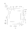
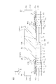
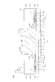
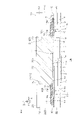
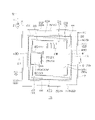
2 チップ
3 第1主面
4 第2主面
5 側面
6 第1半導体領域(半導体基板)
7 第2半導体領域(エピタキシャル層)
11 第1主面電極
17 感光性樹脂
19 熱硬化性樹脂
20 パッド開口
21 樹脂主面
23 樹脂側面
27 マトリクス樹脂
28 フィラー
28a 小径フィラー
28b 中径フィラー
28c 大径フィラー
29 フィラー欠片
29a 第1フィラー欠片
29b 第2フィラー欠片
30 パッド電極
30a 電極面
31 第1パッド電極膜
32 第2パッド電極膜
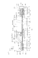
65 ゲート主面電極(第1主面電極)
67 ソース主面電極(第1主面電極)
73 ゲートパッド開口(パッド開口)
74 ソースパッド開口(パッド開口)
80 ゲートパッド電極(パッド電極)
80a 電極面
81 ソースパッド電極(パッド電極)
81a 電極面
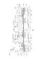
101A 半導体パッケージ
101B 半導体パッケージ
101C 半導体パッケージ
102 パッケージ本体
106 金属板(導体板)
109 端子電極
112 導線(導電接続部材)
122 パッケージ本体
126 第1金属板(導体板、端子電極)
130 第2金属板(導体板、端子電極)
134 端子電極
137 第1導体スペーサ(導電接続部材)
138 第2導体スペーサ(導電接続部材)
139 導線(導電接続部材)
Claims (20)
- ワイドバンドギャップ半導体を含み、主面を有するチップと、
前記主面の上に配置された主面電極と、
マトリクス樹脂および複数のフィラーを含み、前記主面電極の一部を露出させるように前記主面を被覆する熱硬化性樹脂と、を含む、ワイドバンドギャップ半導体装置。 - 前記熱硬化性樹脂は、前記主面電極よりも厚い、請求項1に記載のワイドバンドギャップ半導体装置。
- 複数の前記フィラーは、前記主面電極よりも薄い複数の第1フィラー、および、前記主面電極よりも厚い複数の第2フィラーを含む、請求項1または2に記載のワイドバンドギャップ半導体装置。
- 前記主面電極の周縁部を被覆する感光性樹脂をさらに含み、
前記熱硬化性樹脂は、前記感光性樹脂を被覆している、請求項1~3のいずれか一項に記載のワイドバンドギャップ半導体装置。 - 前記感光性樹脂は、前記主面電極よりも厚く、
前記熱硬化性樹脂は、前記感光性樹脂よりも厚い、請求項4に記載のワイドバンドギャップ半導体装置。 - 複数の前記フィラーは、前記感光性樹脂よりも厚い複数の大径フィラーを含む、請求項5に記載のワイドバンドギャップ半導体装置。
- 前記熱硬化性樹脂は、前記チップよりも厚い、請求項1~6のいずれか一項に記載のワイドバンドギャップ半導体装置。
- 前記主面電極における前記熱硬化性樹脂から露出した部分の上に形成され、前記熱硬化性樹脂から露出した電極面を有するパッド電極をさらに含む、請求項1~7のいずれか一項に記載のワイドバンドギャップ半導体装置。
- 前記電極面は、前記熱硬化性樹脂の外面と1つの平坦面を形成している、請求項8に記載のワイドバンドギャップ半導体装置。
- 前記パッド電極は、前記主面電極を被覆する第1電極膜、および、前記第1電極膜を被覆する第2電極膜を含む積層構造を有している、請求項8または9に記載のワイドバンドギャップ半導体装置。
- 複数の前記フィラーは、前記熱硬化性樹脂の表層部において破断された粒形を有する複数のフィラー欠片を含む、請求項1~10のいずれか一項に記載のワイドバンドギャップ半導体装置。
- 前記チップは、側面を有し、
前記熱硬化性樹脂は、前記側面に連なる樹脂側面を有している、請求項1~11のいずれか一項に記載のワイドバンドギャップ半導体装置。 - 前記樹脂側面は、前記チップの前記側面と1つの研削面を形成している、請求項12に記載のワイドバンドギャップ半導体装置。
- 前記熱硬化性樹脂は、前記チップの周縁部において前記主面を直接被覆する部分を含む、請求項1~13のいずれか一項に記載のワイドバンドギャップ半導体装置。
- 複数の前記主面電極が前記主面の上に配置され、
前記熱硬化性樹脂は、複数の前記主面電極の一部をそれぞれに露出させるように前記主面を被覆している、請求項1~14のいずれか一項に記載のワイドバンドギャップ半導体装置。 - 前記チップは、ワイドバンドギャップ半導体によってそれぞれ構成された半導体基板およびエピタキシャル層を含む積層構造を有し、前記エピタキシャル層によって形成された前記主面を含む、請求項1~15のいずれか一項に記載のワイドバンドギャップ半導体装置。
- 前記チップは、エピタキシャル層からなる単層構造を有している、請求項1~15のいずれか一項に記載のワイドバンドギャップ半導体装置。
- 前記チップに形成された機能デバイスをさらに含み、
前記主面電極は、前記機能デバイスに電気的に接続されている、請求項1~17のいずれか一項に記載のワイドバンドギャップ半導体装置。 - 前記機能デバイスは、ダイオードおよびトランジスタのうちの少なくとも1つを含む、請求項18に記載のワイドバンドギャップ半導体装置。
- モールド樹脂からなるパッケージ本体と、
前記パッケージ本体内に配置された導体板と、
前記パッケージ本体から部分的に露出するように前記導体板から間隔を空けて前記パッケージ本体内に配置された端子電極と、
前記パッケージ本体内において前記導体板の上に配置された請求項1~19のいずれか一項に記載のワイドバンドギャップ半導体装置と、
前記パッケージ本体内において前記端子電極および前記ワイドバンドギャップ半導体装置に電気的に接続された接続部材と、を含む、半導体パッケージ。
Priority Applications (4)
| Application Number | Priority Date | Filing Date | Title |
|---|---|---|---|
| JP2023506844A JPWO2022196158A1 (ja) | 2021-03-18 | 2022-02-03 | |
| DE112022000168.2T DE112022000168T5 (de) | 2021-03-18 | 2022-02-03 | Halbleiterbauteil mit breiter bandlücke |
| CN202280013916.3A CN116830262A (zh) | 2021-03-18 | 2022-02-03 | 宽带隙半导体装置 |
| US18/254,029 US20230335633A1 (en) | 2021-03-18 | 2022-02-03 | Wide bandgap semiconductor device |
Applications Claiming Priority (2)
| Application Number | Priority Date | Filing Date | Title |
|---|---|---|---|
| JP2021-045115 | 2021-03-18 | ||
| JP2021045115 | 2021-03-18 |
Publications (1)
| Publication Number | Publication Date |
|---|---|
| WO2022196158A1 true WO2022196158A1 (ja) | 2022-09-22 |
Family
ID=83322204
Family Applications (1)
| Application Number | Title | Priority Date | Filing Date |
|---|---|---|---|
| PCT/JP2022/004301 WO2022196158A1 (ja) | 2021-03-18 | 2022-02-03 | ワイドバンドギャップ半導体装置 |
Country Status (5)
| Country | Link |
|---|---|
| US (1) | US20230335633A1 (ja) |
| JP (1) | JPWO2022196158A1 (ja) |
| CN (1) | CN116830262A (ja) |
| DE (1) | DE112022000168T5 (ja) |
| WO (1) | WO2022196158A1 (ja) |
Cited By (7)
| Publication number | Priority date | Publication date | Assignee | Title |
|---|---|---|---|---|
| WO2023080082A1 (ja) * | 2021-11-05 | 2023-05-11 | ローム株式会社 | 半導体装置 |
| WO2023080088A1 (ja) * | 2021-11-05 | 2023-05-11 | ローム株式会社 | 半導体装置 |
| WO2023080087A1 (ja) * | 2021-11-05 | 2023-05-11 | ローム株式会社 | 半導体装置 |
| WO2023080086A1 (ja) * | 2021-11-05 | 2023-05-11 | ローム株式会社 | 半導体装置 |
| WO2023080083A1 (ja) * | 2021-11-05 | 2023-05-11 | ローム株式会社 | 半導体装置 |
| WO2023080084A1 (ja) * | 2021-11-05 | 2023-05-11 | ローム株式会社 | 半導体装置 |
| WO2023176056A1 (ja) * | 2022-03-14 | 2023-09-21 | ローム株式会社 | 半導体装置 |
Citations (5)
| Publication number | Priority date | Publication date | Assignee | Title |
|---|---|---|---|---|
| JP2000223693A (ja) * | 1999-01-29 | 2000-08-11 | Sanyo Electric Co Ltd | 半導体装置の製造方法 |
| JP2009188148A (ja) * | 2008-02-06 | 2009-08-20 | Sanyo Electric Co Ltd | 半導体装置およびその製造方法 |
| JP2013239607A (ja) * | 2012-05-16 | 2013-11-28 | Mitsubishi Electric Corp | 半導体装置 |
| JP2019050320A (ja) * | 2017-09-12 | 2019-03-28 | パナソニックIpマネジメント株式会社 | 半導体装置およびその製造方法 |
| WO2020213603A1 (ja) * | 2019-04-19 | 2020-10-22 | ローム株式会社 | SiC半導体装置 |
Family Cites Families (1)
| Publication number | Priority date | Publication date | Assignee | Title |
|---|---|---|---|---|
| JP7371898B2 (ja) | 2019-09-12 | 2023-10-31 | 株式会社スズテック | 播種装置 |
-
2022
- 2022-02-03 WO PCT/JP2022/004301 patent/WO2022196158A1/ja active Application Filing
- 2022-02-03 US US18/254,029 patent/US20230335633A1/en active Pending
- 2022-02-03 JP JP2023506844A patent/JPWO2022196158A1/ja active Pending
- 2022-02-03 CN CN202280013916.3A patent/CN116830262A/zh active Pending
- 2022-02-03 DE DE112022000168.2T patent/DE112022000168T5/de active Pending
Patent Citations (5)
| Publication number | Priority date | Publication date | Assignee | Title |
|---|---|---|---|---|
| JP2000223693A (ja) * | 1999-01-29 | 2000-08-11 | Sanyo Electric Co Ltd | 半導体装置の製造方法 |
| JP2009188148A (ja) * | 2008-02-06 | 2009-08-20 | Sanyo Electric Co Ltd | 半導体装置およびその製造方法 |
| JP2013239607A (ja) * | 2012-05-16 | 2013-11-28 | Mitsubishi Electric Corp | 半導体装置 |
| JP2019050320A (ja) * | 2017-09-12 | 2019-03-28 | パナソニックIpマネジメント株式会社 | 半導体装置およびその製造方法 |
| WO2020213603A1 (ja) * | 2019-04-19 | 2020-10-22 | ローム株式会社 | SiC半導体装置 |
Cited By (7)
| Publication number | Priority date | Publication date | Assignee | Title |
|---|---|---|---|---|
| WO2023080082A1 (ja) * | 2021-11-05 | 2023-05-11 | ローム株式会社 | 半導体装置 |
| WO2023080088A1 (ja) * | 2021-11-05 | 2023-05-11 | ローム株式会社 | 半導体装置 |
| WO2023080087A1 (ja) * | 2021-11-05 | 2023-05-11 | ローム株式会社 | 半導体装置 |
| WO2023080086A1 (ja) * | 2021-11-05 | 2023-05-11 | ローム株式会社 | 半導体装置 |
| WO2023080083A1 (ja) * | 2021-11-05 | 2023-05-11 | ローム株式会社 | 半導体装置 |
| WO2023080084A1 (ja) * | 2021-11-05 | 2023-05-11 | ローム株式会社 | 半導体装置 |
| WO2023176056A1 (ja) * | 2022-03-14 | 2023-09-21 | ローム株式会社 | 半導体装置 |
Also Published As
| Publication number | Publication date |
|---|---|
| JPWO2022196158A1 (ja) | 2022-09-22 |
| US20230335633A1 (en) | 2023-10-19 |
| CN116830262A (zh) | 2023-09-29 |
| DE112022000168T5 (de) | 2023-07-27 |
Similar Documents
| Publication | Publication Date | Title |
|---|---|---|
| WO2022196158A1 (ja) | ワイドバンドギャップ半導体装置 | |
| US9640632B2 (en) | Semiconductor device having improved heat dissipation | |
| JP5712231B2 (ja) | 半導体装置 | |
| US20230223445A1 (en) | SiC SEMICONDUCTOR DEVICE | |
| JP2007049045A (ja) | 半導体発光素子およびこれを備えた半導体装置 | |
| US10727146B2 (en) | Semiconductor device | |
| US20230352392A1 (en) | Semiconductor device | |
| JP7247892B2 (ja) | 炭化珪素半導体装置 | |
| WO2021261102A1 (ja) | 電子部品 | |
| CN108538984B (zh) | 发光二极管结构 | |
| US20240006364A1 (en) | Semiconductor device | |
| WO2021065740A1 (ja) | 半導体装置 | |
| JP7248026B2 (ja) | 炭化珪素半導体装置 | |
| WO2022222042A1 (zh) | 发光二极管芯片 | |
| WO2023080084A1 (ja) | 半導体装置 | |
| WO2023080086A1 (ja) | 半導体装置 | |
| US20230369392A1 (en) | Semiconductor device | |
| WO2023080083A1 (ja) | 半導体装置 | |
| WO2023080087A1 (ja) | 半導体装置 | |
| WO2021261397A1 (ja) | 半導体装置 | |
| WO2023080088A1 (ja) | 半導体装置 | |
| WO2023080085A1 (ja) | 半導体装置の製造方法 | |
| WO2023080082A1 (ja) | 半導体装置 | |
| WO2023080093A1 (ja) | 半導体モジュール | |
| WO2023189054A1 (ja) | 半導体装置 |
Legal Events
| Date | Code | Title | Description |
|---|---|---|---|
| 121 | Ep: the epo has been informed by wipo that ep was designated in this application |
Ref document number: 22770918 Country of ref document: EP Kind code of ref document: A1 |
|
| ENP | Entry into the national phase |
Ref document number: 2023506844 Country of ref document: JP Kind code of ref document: A |
|
| WWE | Wipo information: entry into national phase |
Ref document number: 202280013916.3 Country of ref document: CN |
|
| 122 | Ep: pct application non-entry in european phase |
Ref document number: 22770918 Country of ref document: EP Kind code of ref document: A1 |