WO2022196158A1 - Dispositif semi-conducteur à large bande interdite - Google Patents
Dispositif semi-conducteur à large bande interdite Download PDFInfo
- Publication number
- WO2022196158A1 WO2022196158A1 PCT/JP2022/004301 JP2022004301W WO2022196158A1 WO 2022196158 A1 WO2022196158 A1 WO 2022196158A1 JP 2022004301 W JP2022004301 W JP 2022004301W WO 2022196158 A1 WO2022196158 A1 WO 2022196158A1
- Authority
- WO
- WIPO (PCT)
- Prior art keywords
- electrode
- main surface
- semiconductor device
- wide bandgap
- bandgap semiconductor
- Prior art date
Links
- 239000004065 semiconductor Substances 0.000 title claims abstract description 364
- 239000011347 resin Substances 0.000 claims abstract description 463
- 229920005989 resin Polymers 0.000 claims abstract description 463
- 229920001187 thermosetting polymer Polymers 0.000 claims abstract description 135
- 239000000945 filler Substances 0.000 claims abstract description 114
- 239000011159 matrix material Substances 0.000 claims abstract description 26
- 239000004020 conductor Substances 0.000 claims description 38
- 239000002344 surface layer Substances 0.000 claims description 23
- 239000010410 layer Substances 0.000 claims description 18
- 239000000758 substrate Substances 0.000 claims description 14
- 239000002245 particle Substances 0.000 claims description 8
- 239000002356 single layer Substances 0.000 claims description 8
- 239000012634 fragment Substances 0.000 claims description 5
- 230000002093 peripheral effect Effects 0.000 description 93
- 229910052751 metal Inorganic materials 0.000 description 36
- 239000002184 metal Substances 0.000 description 36
- 239000011229 interlayer Substances 0.000 description 28
- 229910010271 silicon carbide Inorganic materials 0.000 description 23
- HBMJWWWQQXIZIP-UHFFFAOYSA-N silicon carbide Chemical compound [Si+]#[C-] HBMJWWWQQXIZIP-UHFFFAOYSA-N 0.000 description 19
- 125000006850 spacer group Chemical group 0.000 description 19
- KDLHZDBZIXYQEI-UHFFFAOYSA-N Palladium Chemical compound [Pd] KDLHZDBZIXYQEI-UHFFFAOYSA-N 0.000 description 18
- PXHVJJICTQNCMI-UHFFFAOYSA-N Nickel Chemical compound [Ni] PXHVJJICTQNCMI-UHFFFAOYSA-N 0.000 description 16
- 239000013078 crystal Substances 0.000 description 16
- 239000012535 impurity Substances 0.000 description 15
- 239000000463 material Substances 0.000 description 15
- 210000000746 body region Anatomy 0.000 description 14
- 230000000694 effects Effects 0.000 description 13
- PCHJSUWPFVWCPO-UHFFFAOYSA-N gold Chemical compound [Au] PCHJSUWPFVWCPO-UHFFFAOYSA-N 0.000 description 12
- 229910052737 gold Inorganic materials 0.000 description 11
- 239000010931 gold Substances 0.000 description 11
- 229910052763 palladium Inorganic materials 0.000 description 9
- 239000010949 copper Substances 0.000 description 8
- 229910052759 nickel Inorganic materials 0.000 description 8
- VYPSYNLAJGMNEJ-UHFFFAOYSA-N Silicium dioxide Chemical compound O=[Si]=O VYPSYNLAJGMNEJ-UHFFFAOYSA-N 0.000 description 7
- XUIMIQQOPSSXEZ-UHFFFAOYSA-N Silicon Chemical compound [Si] XUIMIQQOPSSXEZ-UHFFFAOYSA-N 0.000 description 6
- 229910052710 silicon Inorganic materials 0.000 description 6
- 239000010703 silicon Substances 0.000 description 6
- 229910052814 silicon oxide Inorganic materials 0.000 description 6
- 229910052581 Si3N4 Inorganic materials 0.000 description 4
- ATJFFYVFTNAWJD-UHFFFAOYSA-N Tin Chemical compound [Sn] ATJFFYVFTNAWJD-UHFFFAOYSA-N 0.000 description 4
- 239000003822 epoxy resin Substances 0.000 description 4
- 239000012212 insulator Substances 0.000 description 4
- 230000004048 modification Effects 0.000 description 4
- 238000012986 modification Methods 0.000 description 4
- 238000005192 partition Methods 0.000 description 4
- 229920000647 polyepoxide Polymers 0.000 description 4
- HQVNEWCFYHHQES-UHFFFAOYSA-N silicon nitride Chemical compound N12[Si]34N5[Si]62N3[Si]51N64 HQVNEWCFYHHQES-UHFFFAOYSA-N 0.000 description 4
- 229910000679 solder Inorganic materials 0.000 description 4
- 229910045601 alloy Inorganic materials 0.000 description 3
- 239000000956 alloy Substances 0.000 description 3
- 230000004888 barrier function Effects 0.000 description 3
- 230000007423 decrease Effects 0.000 description 3
- 239000011800 void material Substances 0.000 description 3
- RYGMFSIKBFXOCR-UHFFFAOYSA-N Copper Chemical compound [Cu] RYGMFSIKBFXOCR-UHFFFAOYSA-N 0.000 description 2
- 229910002601 GaN Inorganic materials 0.000 description 2
- JMASRVWKEDWRBT-UHFFFAOYSA-N Gallium nitride Chemical compound [Ga]#N JMASRVWKEDWRBT-UHFFFAOYSA-N 0.000 description 2
- 229910052782 aluminium Inorganic materials 0.000 description 2
- XAGFODPZIPBFFR-UHFFFAOYSA-N aluminium Chemical compound [Al] XAGFODPZIPBFFR-UHFFFAOYSA-N 0.000 description 2
- 230000015572 biosynthetic process Effects 0.000 description 2
- 230000005684 electric field Effects 0.000 description 2
- 238000007772 electroless plating Methods 0.000 description 2
- 238000009713 electroplating Methods 0.000 description 2
- 238000004299 exfoliation Methods 0.000 description 2
- 238000007747 plating Methods 0.000 description 2
- 229920002577 polybenzoxazole Polymers 0.000 description 2
- 229920001721 polyimide Polymers 0.000 description 2
- 230000001681 protective effect Effects 0.000 description 2
- 238000000926 separation method Methods 0.000 description 2
- KXGFMDJXCMQABM-UHFFFAOYSA-N 2-methoxy-6-methylphenol Chemical compound [CH]OC1=CC=CC([CH])=C1O KXGFMDJXCMQABM-UHFFFAOYSA-N 0.000 description 1
- 229910016570 AlCu Inorganic materials 0.000 description 1
- 229910000789 Aluminium-silicon alloy Inorganic materials 0.000 description 1
- OKTJSMMVPCPJKN-UHFFFAOYSA-N Carbon Chemical compound [C] OKTJSMMVPCPJKN-UHFFFAOYSA-N 0.000 description 1
- 239000004952 Polyamide Substances 0.000 description 1
- 229910052799 carbon Inorganic materials 0.000 description 1
- 239000006229 carbon black Substances 0.000 description 1
- 230000015556 catabolic process Effects 0.000 description 1
- 239000000919 ceramic Substances 0.000 description 1
- 239000011248 coating agent Substances 0.000 description 1
- 238000000576 coating method Methods 0.000 description 1
- 238000004040 coloring Methods 0.000 description 1
- 229910052802 copper Inorganic materials 0.000 description 1
- 238000010586 diagram Methods 0.000 description 1
- 229910003460 diamond Inorganic materials 0.000 description 1
- 239000010432 diamond Substances 0.000 description 1
- 239000005007 epoxy-phenolic resin Substances 0.000 description 1
- 230000005669 field effect Effects 0.000 description 1
- 239000000446 fuel Substances 0.000 description 1
- 239000011810 insulating material Substances 0.000 description 1
- -1 oxide Substances 0.000 description 1
- 229920001568 phenolic resin Polymers 0.000 description 1
- 229920002647 polyamide Polymers 0.000 description 1
- 229910021420 polycrystalline silicon Inorganic materials 0.000 description 1
- 239000009719 polyimide resin Substances 0.000 description 1
- 229920005591 polysilicon Polymers 0.000 description 1
- 239000011241 protective layer Substances 0.000 description 1
- 238000007789 sealing Methods 0.000 description 1
- 238000004544 sputter deposition Methods 0.000 description 1
Images


Classifications
-
- H—ELECTRICITY
- H01—ELECTRIC ELEMENTS
- H01L—SEMICONDUCTOR DEVICES NOT COVERED BY CLASS H10
- H01L23/00—Details of semiconductor or other solid state devices
- H01L23/28—Encapsulations, e.g. encapsulating layers, coatings, e.g. for protection
- H01L23/31—Encapsulations, e.g. encapsulating layers, coatings, e.g. for protection characterised by the arrangement or shape
- H01L23/3157—Partial encapsulation or coating
- H01L23/3171—Partial encapsulation or coating the coating being directly applied to the semiconductor body, e.g. passivation layer
-
- H—ELECTRICITY
- H01—ELECTRIC ELEMENTS
- H01L—SEMICONDUCTOR DEVICES NOT COVERED BY CLASS H10
- H01L29/00—Semiconductor devices adapted for rectifying, amplifying, oscillating or switching, or capacitors or resistors with at least one potential-jump barrier or surface barrier, e.g. PN junction depletion layer or carrier concentration layer; Details of semiconductor bodies or of electrodes thereof ; Multistep manufacturing processes therefor
- H01L29/66—Types of semiconductor device ; Multistep manufacturing processes therefor
- H01L29/68—Types of semiconductor device ; Multistep manufacturing processes therefor controllable by only the electric current supplied, or only the electric potential applied, to an electrode which does not carry the current to be rectified, amplified or switched
- H01L29/76—Unipolar devices, e.g. field effect transistors
- H01L29/772—Field effect transistors
- H01L29/78—Field effect transistors with field effect produced by an insulated gate
- H01L29/7801—DMOS transistors, i.e. MISFETs with a channel accommodating body or base region adjoining a drain drift region
- H01L29/7802—Vertical DMOS transistors, i.e. VDMOS transistors
- H01L29/7803—Vertical DMOS transistors, i.e. VDMOS transistors structurally associated with at least one other device
- H01L29/7806—Vertical DMOS transistors, i.e. VDMOS transistors structurally associated with at least one other device the other device being a Schottky barrier diode
-
- H—ELECTRICITY
- H01—ELECTRIC ELEMENTS
- H01L—SEMICONDUCTOR DEVICES NOT COVERED BY CLASS H10
- H01L23/00—Details of semiconductor or other solid state devices
- H01L23/28—Encapsulations, e.g. encapsulating layers, coatings, e.g. for protection
- H01L23/29—Encapsulations, e.g. encapsulating layers, coatings, e.g. for protection characterised by the material, e.g. carbon
- H01L23/293—Organic, e.g. plastic
- H01L23/295—Organic, e.g. plastic containing a filler
-
- H—ELECTRICITY
- H01—ELECTRIC ELEMENTS
- H01L—SEMICONDUCTOR DEVICES NOT COVERED BY CLASS H10
- H01L23/00—Details of semiconductor or other solid state devices
- H01L23/28—Encapsulations, e.g. encapsulating layers, coatings, e.g. for protection
- H01L23/31—Encapsulations, e.g. encapsulating layers, coatings, e.g. for protection characterised by the arrangement or shape
- H01L23/3157—Partial encapsulation or coating
- H01L23/3192—Multilayer coating
-
- H—ELECTRICITY
- H01—ELECTRIC ELEMENTS
- H01L—SEMICONDUCTOR DEVICES NOT COVERED BY CLASS H10
- H01L24/00—Arrangements for connecting or disconnecting semiconductor or solid-state bodies; Methods or apparatus related thereto
- H01L24/01—Means for bonding being attached to, or being formed on, the surface to be connected, e.g. chip-to-package, die-attach, "first-level" interconnects; Manufacturing methods related thereto
- H01L24/02—Bonding areas ; Manufacturing methods related thereto
- H01L24/07—Structure, shape, material or disposition of the bonding areas after the connecting process
- H01L24/08—Structure, shape, material or disposition of the bonding areas after the connecting process of an individual bonding area
-
- H—ELECTRICITY
- H01—ELECTRIC ELEMENTS
- H01L—SEMICONDUCTOR DEVICES NOT COVERED BY CLASS H10
- H01L24/00—Arrangements for connecting or disconnecting semiconductor or solid-state bodies; Methods or apparatus related thereto
- H01L24/01—Means for bonding being attached to, or being formed on, the surface to be connected, e.g. chip-to-package, die-attach, "first-level" interconnects; Manufacturing methods related thereto
- H01L24/10—Bump connectors ; Manufacturing methods related thereto
- H01L24/15—Structure, shape, material or disposition of the bump connectors after the connecting process
- H01L24/16—Structure, shape, material or disposition of the bump connectors after the connecting process of an individual bump connector
-
- H—ELECTRICITY
- H01—ELECTRIC ELEMENTS
- H01L—SEMICONDUCTOR DEVICES NOT COVERED BY CLASS H10
- H01L24/00—Arrangements for connecting or disconnecting semiconductor or solid-state bodies; Methods or apparatus related thereto
- H01L24/01—Means for bonding being attached to, or being formed on, the surface to be connected, e.g. chip-to-package, die-attach, "first-level" interconnects; Manufacturing methods related thereto
- H01L24/42—Wire connectors; Manufacturing methods related thereto
- H01L24/47—Structure, shape, material or disposition of the wire connectors after the connecting process
- H01L24/48—Structure, shape, material or disposition of the wire connectors after the connecting process of an individual wire connector
-
- H—ELECTRICITY
- H01—ELECTRIC ELEMENTS
- H01L—SEMICONDUCTOR DEVICES NOT COVERED BY CLASS H10
- H01L24/00—Arrangements for connecting or disconnecting semiconductor or solid-state bodies; Methods or apparatus related thereto
- H01L24/73—Means for bonding being of different types provided for in two or more of groups H01L24/10, H01L24/18, H01L24/26, H01L24/34, H01L24/42, H01L24/50, H01L24/63, H01L24/71
-
- H—ELECTRICITY
- H01—ELECTRIC ELEMENTS
- H01L—SEMICONDUCTOR DEVICES NOT COVERED BY CLASS H10
- H01L29/00—Semiconductor devices adapted for rectifying, amplifying, oscillating or switching, or capacitors or resistors with at least one potential-jump barrier or surface barrier, e.g. PN junction depletion layer or carrier concentration layer; Details of semiconductor bodies or of electrodes thereof ; Multistep manufacturing processes therefor
- H01L29/02—Semiconductor bodies ; Multistep manufacturing processes therefor
- H01L29/12—Semiconductor bodies ; Multistep manufacturing processes therefor characterised by the materials of which they are formed
- H01L29/16—Semiconductor bodies ; Multistep manufacturing processes therefor characterised by the materials of which they are formed including, apart from doping materials or other impurities, only elements of Group IV of the Periodic System
- H01L29/1608—Silicon carbide
-
- H—ELECTRICITY
- H01—ELECTRIC ELEMENTS
- H01L—SEMICONDUCTOR DEVICES NOT COVERED BY CLASS H10
- H01L29/00—Semiconductor devices adapted for rectifying, amplifying, oscillating or switching, or capacitors or resistors with at least one potential-jump barrier or surface barrier, e.g. PN junction depletion layer or carrier concentration layer; Details of semiconductor bodies or of electrodes thereof ; Multistep manufacturing processes therefor
- H01L29/40—Electrodes ; Multistep manufacturing processes therefor
- H01L29/41—Electrodes ; Multistep manufacturing processes therefor characterised by their shape, relative sizes or dispositions
- H01L29/417—Electrodes ; Multistep manufacturing processes therefor characterised by their shape, relative sizes or dispositions carrying the current to be rectified, amplified or switched
- H01L29/41725—Source or drain electrodes for field effect devices
- H01L29/41766—Source or drain electrodes for field effect devices with at least part of the source or drain electrode having contact below the semiconductor surface, e.g. the source or drain electrode formed at least partially in a groove or with inclusions of conductor inside the semiconductor
-
- H—ELECTRICITY
- H01—ELECTRIC ELEMENTS
- H01L—SEMICONDUCTOR DEVICES NOT COVERED BY CLASS H10
- H01L29/00—Semiconductor devices adapted for rectifying, amplifying, oscillating or switching, or capacitors or resistors with at least one potential-jump barrier or surface barrier, e.g. PN junction depletion layer or carrier concentration layer; Details of semiconductor bodies or of electrodes thereof ; Multistep manufacturing processes therefor
- H01L29/66—Types of semiconductor device ; Multistep manufacturing processes therefor
- H01L29/68—Types of semiconductor device ; Multistep manufacturing processes therefor controllable by only the electric current supplied, or only the electric potential applied, to an electrode which does not carry the current to be rectified, amplified or switched
- H01L29/76—Unipolar devices, e.g. field effect transistors
- H01L29/772—Field effect transistors
- H01L29/78—Field effect transistors with field effect produced by an insulated gate
- H01L29/7801—DMOS transistors, i.e. MISFETs with a channel accommodating body or base region adjoining a drain drift region
- H01L29/7802—Vertical DMOS transistors, i.e. VDMOS transistors
- H01L29/7811—Vertical DMOS transistors, i.e. VDMOS transistors with an edge termination structure
-
- H—ELECTRICITY
- H01—ELECTRIC ELEMENTS
- H01L—SEMICONDUCTOR DEVICES NOT COVERED BY CLASS H10
- H01L29/00—Semiconductor devices adapted for rectifying, amplifying, oscillating or switching, or capacitors or resistors with at least one potential-jump barrier or surface barrier, e.g. PN junction depletion layer or carrier concentration layer; Details of semiconductor bodies or of electrodes thereof ; Multistep manufacturing processes therefor
- H01L29/66—Types of semiconductor device ; Multistep manufacturing processes therefor
- H01L29/68—Types of semiconductor device ; Multistep manufacturing processes therefor controllable by only the electric current supplied, or only the electric potential applied, to an electrode which does not carry the current to be rectified, amplified or switched
- H01L29/76—Unipolar devices, e.g. field effect transistors
- H01L29/772—Field effect transistors
- H01L29/78—Field effect transistors with field effect produced by an insulated gate
- H01L29/7801—DMOS transistors, i.e. MISFETs with a channel accommodating body or base region adjoining a drain drift region
- H01L29/7802—Vertical DMOS transistors, i.e. VDMOS transistors
- H01L29/7813—Vertical DMOS transistors, i.e. VDMOS transistors with trench gate electrode, e.g. UMOS transistors
-
- H—ELECTRICITY
- H01—ELECTRIC ELEMENTS
- H01L—SEMICONDUCTOR DEVICES NOT COVERED BY CLASS H10
- H01L29/00—Semiconductor devices adapted for rectifying, amplifying, oscillating or switching, or capacitors or resistors with at least one potential-jump barrier or surface barrier, e.g. PN junction depletion layer or carrier concentration layer; Details of semiconductor bodies or of electrodes thereof ; Multistep manufacturing processes therefor
- H01L29/66—Types of semiconductor device ; Multistep manufacturing processes therefor
- H01L29/68—Types of semiconductor device ; Multistep manufacturing processes therefor controllable by only the electric current supplied, or only the electric potential applied, to an electrode which does not carry the current to be rectified, amplified or switched
- H01L29/76—Unipolar devices, e.g. field effect transistors
- H01L29/772—Field effect transistors
- H01L29/78—Field effect transistors with field effect produced by an insulated gate
- H01L29/7801—DMOS transistors, i.e. MISFETs with a channel accommodating body or base region adjoining a drain drift region
- H01L29/7816—Lateral DMOS transistors, i.e. LDMOS transistors
- H01L29/7825—Lateral DMOS transistors, i.e. LDMOS transistors with trench gate electrode
-
- H—ELECTRICITY
- H01—ELECTRIC ELEMENTS
- H01L—SEMICONDUCTOR DEVICES NOT COVERED BY CLASS H10
- H01L29/00—Semiconductor devices adapted for rectifying, amplifying, oscillating or switching, or capacitors or resistors with at least one potential-jump barrier or surface barrier, e.g. PN junction depletion layer or carrier concentration layer; Details of semiconductor bodies or of electrodes thereof ; Multistep manufacturing processes therefor
- H01L29/66—Types of semiconductor device ; Multistep manufacturing processes therefor
- H01L29/86—Types of semiconductor device ; Multistep manufacturing processes therefor controllable only by variation of the electric current supplied, or only the electric potential applied, to one or more of the electrodes carrying the current to be rectified, amplified, oscillated or switched
- H01L29/861—Diodes
- H01L29/872—Schottky diodes
-
- H—ELECTRICITY
- H01—ELECTRIC ELEMENTS
- H01L—SEMICONDUCTOR DEVICES NOT COVERED BY CLASS H10
- H01L2224/00—Indexing scheme for arrangements for connecting or disconnecting semiconductor or solid-state bodies and methods related thereto as covered by H01L24/00
- H01L2224/01—Means for bonding being attached to, or being formed on, the surface to be connected, e.g. chip-to-package, die-attach, "first-level" interconnects; Manufacturing methods related thereto
- H01L2224/02—Bonding areas; Manufacturing methods related thereto
- H01L2224/07—Structure, shape, material or disposition of the bonding areas after the connecting process
- H01L2224/08—Structure, shape, material or disposition of the bonding areas after the connecting process of an individual bonding area
- H01L2224/0801—Structure
-
- H—ELECTRICITY
- H01—ELECTRIC ELEMENTS
- H01L—SEMICONDUCTOR DEVICES NOT COVERED BY CLASS H10
- H01L2224/00—Indexing scheme for arrangements for connecting or disconnecting semiconductor or solid-state bodies and methods related thereto as covered by H01L24/00
- H01L2224/01—Means for bonding being attached to, or being formed on, the surface to be connected, e.g. chip-to-package, die-attach, "first-level" interconnects; Manufacturing methods related thereto
- H01L2224/42—Wire connectors; Manufacturing methods related thereto
- H01L2224/47—Structure, shape, material or disposition of the wire connectors after the connecting process
- H01L2224/48—Structure, shape, material or disposition of the wire connectors after the connecting process of an individual wire connector
- H01L2224/481—Disposition
- H01L2224/48151—Connecting between a semiconductor or solid-state body and an item not being a semiconductor or solid-state body, e.g. chip-to-substrate, chip-to-passive
- H01L2224/48221—Connecting between a semiconductor or solid-state body and an item not being a semiconductor or solid-state body, e.g. chip-to-substrate, chip-to-passive the body and the item being stacked
- H01L2224/48225—Connecting between a semiconductor or solid-state body and an item not being a semiconductor or solid-state body, e.g. chip-to-substrate, chip-to-passive the body and the item being stacked the item being non-metallic, e.g. insulating substrate with or without metallisation
- H01L2224/48227—Connecting between a semiconductor or solid-state body and an item not being a semiconductor or solid-state body, e.g. chip-to-substrate, chip-to-passive the body and the item being stacked the item being non-metallic, e.g. insulating substrate with or without metallisation connecting the wire to a bond pad of the item
-
- H—ELECTRICITY
- H01—ELECTRIC ELEMENTS
- H01L—SEMICONDUCTOR DEVICES NOT COVERED BY CLASS H10
- H01L2224/00—Indexing scheme for arrangements for connecting or disconnecting semiconductor or solid-state bodies and methods related thereto as covered by H01L24/00
- H01L2224/73—Means for bonding being of different types provided for in two or more of groups H01L2224/10, H01L2224/18, H01L2224/26, H01L2224/34, H01L2224/42, H01L2224/50, H01L2224/63, H01L2224/71
- H01L2224/732—Location after the connecting process
- H01L2224/73201—Location after the connecting process on the same surface
- H01L2224/73215—Layer and wire connectors
-
- H—ELECTRICITY
- H01—ELECTRIC ELEMENTS
- H01L—SEMICONDUCTOR DEVICES NOT COVERED BY CLASS H10
- H01L23/00—Details of semiconductor or other solid state devices
- H01L23/02—Containers; Seals
- H01L23/04—Containers; Seals characterised by the shape of the container or parts, e.g. caps, walls
- H01L23/043—Containers; Seals characterised by the shape of the container or parts, e.g. caps, walls the container being a hollow construction and having a conductive base as a mounting as well as a lead for the semiconductor body
- H01L23/051—Containers; Seals characterised by the shape of the container or parts, e.g. caps, walls the container being a hollow construction and having a conductive base as a mounting as well as a lead for the semiconductor body another lead being formed by a cover plate parallel to the base plate, e.g. sandwich type
-
- H—ELECTRICITY
- H01—ELECTRIC ELEMENTS
- H01L—SEMICONDUCTOR DEVICES NOT COVERED BY CLASS H10
- H01L23/00—Details of semiconductor or other solid state devices
- H01L23/28—Encapsulations, e.g. encapsulating layers, coatings, e.g. for protection
- H01L23/31—Encapsulations, e.g. encapsulating layers, coatings, e.g. for protection characterised by the arrangement or shape
- H01L23/3107—Encapsulations, e.g. encapsulating layers, coatings, e.g. for protection characterised by the arrangement or shape the device being completely enclosed
- H01L23/3114—Encapsulations, e.g. encapsulating layers, coatings, e.g. for protection characterised by the arrangement or shape the device being completely enclosed the device being a chip scale package, e.g. CSP
-
- H—ELECTRICITY
- H01—ELECTRIC ELEMENTS
- H01L—SEMICONDUCTOR DEVICES NOT COVERED BY CLASS H10
- H01L29/00—Semiconductor devices adapted for rectifying, amplifying, oscillating or switching, or capacitors or resistors with at least one potential-jump barrier or surface barrier, e.g. PN junction depletion layer or carrier concentration layer; Details of semiconductor bodies or of electrodes thereof ; Multistep manufacturing processes therefor
- H01L29/02—Semiconductor bodies ; Multistep manufacturing processes therefor
- H01L29/04—Semiconductor bodies ; Multistep manufacturing processes therefor characterised by their crystalline structure, e.g. polycrystalline, cubic or particular orientation of crystalline planes
- H01L29/045—Semiconductor bodies ; Multistep manufacturing processes therefor characterised by their crystalline structure, e.g. polycrystalline, cubic or particular orientation of crystalline planes by their particular orientation of crystalline planes
-
- H—ELECTRICITY
- H01—ELECTRIC ELEMENTS
- H01L—SEMICONDUCTOR DEVICES NOT COVERED BY CLASS H10
- H01L29/00—Semiconductor devices adapted for rectifying, amplifying, oscillating or switching, or capacitors or resistors with at least one potential-jump barrier or surface barrier, e.g. PN junction depletion layer or carrier concentration layer; Details of semiconductor bodies or of electrodes thereof ; Multistep manufacturing processes therefor
- H01L29/02—Semiconductor bodies ; Multistep manufacturing processes therefor
- H01L29/06—Semiconductor bodies ; Multistep manufacturing processes therefor characterised by their shape; characterised by the shapes, relative sizes, or dispositions of the semiconductor regions ; characterised by the concentration or distribution of impurities within semiconductor regions
- H01L29/0603—Semiconductor bodies ; Multistep manufacturing processes therefor characterised by their shape; characterised by the shapes, relative sizes, or dispositions of the semiconductor regions ; characterised by the concentration or distribution of impurities within semiconductor regions characterised by particular constructional design considerations, e.g. for preventing surface leakage, for controlling electric field concentration or for internal isolations regions
- H01L29/0607—Semiconductor bodies ; Multistep manufacturing processes therefor characterised by their shape; characterised by the shapes, relative sizes, or dispositions of the semiconductor regions ; characterised by the concentration or distribution of impurities within semiconductor regions characterised by particular constructional design considerations, e.g. for preventing surface leakage, for controlling electric field concentration or for internal isolations regions for preventing surface leakage or controlling electric field concentration
- H01L29/0611—Semiconductor bodies ; Multistep manufacturing processes therefor characterised by their shape; characterised by the shapes, relative sizes, or dispositions of the semiconductor regions ; characterised by the concentration or distribution of impurities within semiconductor regions characterised by particular constructional design considerations, e.g. for preventing surface leakage, for controlling electric field concentration or for internal isolations regions for preventing surface leakage or controlling electric field concentration for increasing or controlling the breakdown voltage of reverse biased devices
- H01L29/0615—Semiconductor bodies ; Multistep manufacturing processes therefor characterised by their shape; characterised by the shapes, relative sizes, or dispositions of the semiconductor regions ; characterised by the concentration or distribution of impurities within semiconductor regions characterised by particular constructional design considerations, e.g. for preventing surface leakage, for controlling electric field concentration or for internal isolations regions for preventing surface leakage or controlling electric field concentration for increasing or controlling the breakdown voltage of reverse biased devices by the doping profile or the shape or the arrangement of the PN junction, or with supplementary regions, e.g. junction termination extension [JTE]
- H01L29/0619—Semiconductor bodies ; Multistep manufacturing processes therefor characterised by their shape; characterised by the shapes, relative sizes, or dispositions of the semiconductor regions ; characterised by the concentration or distribution of impurities within semiconductor regions characterised by particular constructional design considerations, e.g. for preventing surface leakage, for controlling electric field concentration or for internal isolations regions for preventing surface leakage or controlling electric field concentration for increasing or controlling the breakdown voltage of reverse biased devices by the doping profile or the shape or the arrangement of the PN junction, or with supplementary regions, e.g. junction termination extension [JTE] with a supplementary region doped oppositely to or in rectifying contact with the semiconductor containing or contacting region, e.g. guard rings with PN or Schottky junction
-
- H—ELECTRICITY
- H01—ELECTRIC ELEMENTS
- H01L—SEMICONDUCTOR DEVICES NOT COVERED BY CLASS H10
- H01L29/00—Semiconductor devices adapted for rectifying, amplifying, oscillating or switching, or capacitors or resistors with at least one potential-jump barrier or surface barrier, e.g. PN junction depletion layer or carrier concentration layer; Details of semiconductor bodies or of electrodes thereof ; Multistep manufacturing processes therefor
- H01L29/02—Semiconductor bodies ; Multistep manufacturing processes therefor
- H01L29/06—Semiconductor bodies ; Multistep manufacturing processes therefor characterised by their shape; characterised by the shapes, relative sizes, or dispositions of the semiconductor regions ; characterised by the concentration or distribution of impurities within semiconductor regions
- H01L29/0684—Semiconductor bodies ; Multistep manufacturing processes therefor characterised by their shape; characterised by the shapes, relative sizes, or dispositions of the semiconductor regions ; characterised by the concentration or distribution of impurities within semiconductor regions characterised by the shape, relative sizes or dispositions of the semiconductor regions or junctions between the regions
- H01L29/0692—Surface layout
- H01L29/0696—Surface layout of cellular field-effect devices, e.g. multicellular DMOS transistors or IGBTs
-
- H—ELECTRICITY
- H01—ELECTRIC ELEMENTS
- H01L—SEMICONDUCTOR DEVICES NOT COVERED BY CLASS H10
- H01L29/00—Semiconductor devices adapted for rectifying, amplifying, oscillating or switching, or capacitors or resistors with at least one potential-jump barrier or surface barrier, e.g. PN junction depletion layer or carrier concentration layer; Details of semiconductor bodies or of electrodes thereof ; Multistep manufacturing processes therefor
- H01L29/02—Semiconductor bodies ; Multistep manufacturing processes therefor
- H01L29/06—Semiconductor bodies ; Multistep manufacturing processes therefor characterised by their shape; characterised by the shapes, relative sizes, or dispositions of the semiconductor regions ; characterised by the concentration or distribution of impurities within semiconductor regions
- H01L29/10—Semiconductor bodies ; Multistep manufacturing processes therefor characterised by their shape; characterised by the shapes, relative sizes, or dispositions of the semiconductor regions ; characterised by the concentration or distribution of impurities within semiconductor regions with semiconductor regions connected to an electrode not carrying current to be rectified, amplified or switched and such electrode being part of a semiconductor device which comprises three or more electrodes
- H01L29/1095—Body region, i.e. base region, of DMOS transistors or IGBTs
-
- H—ELECTRICITY
- H01—ELECTRIC ELEMENTS
- H01L—SEMICONDUCTOR DEVICES NOT COVERED BY CLASS H10
- H01L29/00—Semiconductor devices adapted for rectifying, amplifying, oscillating or switching, or capacitors or resistors with at least one potential-jump barrier or surface barrier, e.g. PN junction depletion layer or carrier concentration layer; Details of semiconductor bodies or of electrodes thereof ; Multistep manufacturing processes therefor
- H01L29/40—Electrodes ; Multistep manufacturing processes therefor
- H01L29/402—Field plates
- H01L29/407—Recessed field plates, e.g. trench field plates, buried field plates
-
- H—ELECTRICITY
- H01—ELECTRIC ELEMENTS
- H01L—SEMICONDUCTOR DEVICES NOT COVERED BY CLASS H10
- H01L2924/00—Indexing scheme for arrangements or methods for connecting or disconnecting semiconductor or solid-state bodies as covered by H01L24/00
- H01L2924/06—Polymers
- H01L2924/078—Adhesive characteristics other than chemical
- H01L2924/07802—Adhesive characteristics other than chemical not being an ohmic electrical conductor
-
- H—ELECTRICITY
- H01—ELECTRIC ELEMENTS
- H01L—SEMICONDUCTOR DEVICES NOT COVERED BY CLASS H10
- H01L2924/00—Indexing scheme for arrangements or methods for connecting or disconnecting semiconductor or solid-state bodies as covered by H01L24/00
- H01L2924/10—Details of semiconductor or other solid state devices to be connected
- H01L2924/11—Device type
- H01L2924/12—Passive devices, e.g. 2 terminal devices
- H01L2924/1203—Rectifying Diode
- H01L2924/12032—Schottky diode
-
- H—ELECTRICITY
- H01—ELECTRIC ELEMENTS
- H01L—SEMICONDUCTOR DEVICES NOT COVERED BY CLASS H10
- H01L2924/00—Indexing scheme for arrangements or methods for connecting or disconnecting semiconductor or solid-state bodies as covered by H01L24/00
- H01L2924/10—Details of semiconductor or other solid state devices to be connected
- H01L2924/11—Device type
- H01L2924/13—Discrete devices, e.g. 3 terminal devices
- H01L2924/1304—Transistor
- H01L2924/1306—Field-effect transistor [FET]
Definitions
- Patent Document 1 discloses a semiconductor device including a semiconductor substrate, electrodes and an organic protective layer.
- the semiconductor substrate is made of SiC.
- An electrode is formed on the semiconductor substrate.
- the organic protective film partially covers the electrodes.
- One embodiment provides a wide bandgap semiconductor device that can improve reliability.
- One embodiment includes a wide band gap semiconductor, a chip having a main surface, a main surface electrode disposed on the main surface, a matrix resin and a plurality of fillers, and a part of the main surface electrode and a thermosetting resin coating the main surface in an exposed manner.
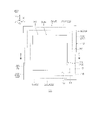
- FIG. 1 is a perspective view showing the wide bandgap semiconductor device according to the first embodiment.
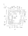
- 2 is a plan view of the wide bandgap semiconductor device shown in FIG. 1.
- FIG. 3 is a cross-sectional view taken along line III-III shown in FIG.
- FIG. 4 is an enlarged view of area IV shown in FIG.
- FIG. 5 is a cross-sectional view corresponding to FIG. 3 and showing a wide bandgap semiconductor device according to the second embodiment.
- FIG. 6 is a cross-sectional view corresponding to FIG. 3 and showing a wide bandgap semiconductor device according to the third embodiment.
- FIG. 7 is a cross-sectional view corresponding to FIG. 3 and showing a wide bandgap semiconductor device according to a fourth embodiment.
- FIG. 1 is a perspective view showing the wide bandgap semiconductor device according to the first embodiment.
- FIG. 3 is a cross-sectional view taken along line III-III shown in FIG.
- FIG. 4 is an enlarged view of area
- FIG. 8 is a cross-sectional view corresponding to FIG. 3 and showing a wide bandgap semiconductor device according to a fifth embodiment.
- FIG. 9 is a cross-sectional view corresponding to FIG. 3 and showing a wide bandgap semiconductor device according to the sixth embodiment.
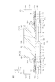
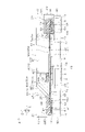
- FIG. 10 is a perspective view showing a wide bandgap semiconductor device according to the seventh embodiment.
- 11 is a plan view of the wide bandgap semiconductor device shown in FIG. 10.
- FIG. 12 is a cross-sectional view taken along line XII-XII shown in FIG. 11.
- FIG. 13 is a plan view showing the region XIII shown in FIG. 11 together with the internal structure.
- 14 is a cross-sectional view taken along line XIV-XIV shown in FIG. 13.
- FIG. 15 is an enlarged view of region XV shown in FIG.
- FIG. 16 is a cross-sectional view corresponding to FIG. 12 and showing the wide bandgap semiconductor device according to the eighth embodiment.
- FIG. 17 is a cross-sectional view corresponding to FIG. 12 and showing the wide bandgap semiconductor device according to the ninth embodiment.
- FIG. 18 is a cross-sectional view corresponding to FIG. 12 and showing the wide bandgap semiconductor device according to the tenth embodiment.
- FIG. 19 is a cross-sectional view corresponding to FIG. 12 and showing the wide bandgap semiconductor device according to the eleventh embodiment.
- FIG. 20 is a cross-sectional view corresponding to FIG. 12 and showing a wide bandgap semiconductor device according to the twelfth embodiment.
- FIG. 21 is a sectional view corresponding to FIG. 3 and showing a modification of the pad electrode.
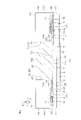
- FIG. 22 is a plan view showing a semiconductor package on which wide bandgap semiconductor devices according to the first to sixth embodiments are mounted.
- FIG. 23 is a plan view showing a semiconductor package on which wide bandgap semiconductor devices according to seventh to twelfth embodiments are mounted.
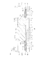
- FIG. 24 is a perspective view showing a semiconductor package in which the wide bandgap semiconductor devices according to the first to sixth embodiments and the wide bandgap semiconductor devices according to the seventh to twelfth embodiments are mounted.
- 25 is an exploded perspective view of the semiconductor package shown in FIG. 24.
- FIG. 26 is a cross-sectional view taken along line XXVI-XXVI shown in FIG. 24.
- FIG. 1 is a perspective view showing a wide bandgap semiconductor device 1A according to the first embodiment.
- FIG. 2 is a plan view of wide bandgap semiconductor device 1A shown in FIG.
- FIG. 3 is a cross-sectional view taken along line III-III shown in FIG.
- FIG. 4 is an enlarged view of area IV shown in FIG.
- wide bandgap semiconductor device 1A is a semiconductor device including an SBD (Schottky Barrier Diode) as an example of a functional device.
- a wide bandgap semiconductor device 1A is made of a wide bandgap semiconductor and includes a chip 2 formed in a hexahedral shape (specifically, a rectangular parallelepiped shape). Chip 2 may also be referred to as a "semiconductor chip” or a "wide bandgap semiconductor chip”.
- a wide bandgap semiconductor is a semiconductor having a bandgap that exceeds the bandgap of Si (silicon).
- the chip 2, in this embodiment, is a SiC chip made of a hexagonal SiC (silicon carbide) single crystal as an example of a wide bandgap semiconductor. That is, the wide bandgap semiconductor device 1A is a SiC semiconductor device. Hexagonal SiC single crystals have a plurality of polytypes including 2H (Hexagonal)-SiC single crystals, 4H-SiC single crystals, 6H-SiC single crystals and the like. This embodiment shows an example in which the chip 2 is made of 4H—SiC single crystal, but other polytypes are not excluded.
- the chip 2 has a first principal surface 3 on one side, a second principal surface 4 on the other side, and a side surface 5 connecting the first principal surface 3 and the second principal surface 4 .
- the first main surface 3 and the second main surface 4 are formed in a quadrangular shape when viewed from the normal direction Z (hereinafter simply referred to as "plan view").
- the second main surface 4 is preferably a ground surface having grinding marks.
- the side surface 5 includes first to fourth side surfaces 5A to 5D.
- the first side surface 5A and the second side surface 5B extend in the first direction X along the first main surface 3 and face the second direction Y intersecting (specifically, perpendicular to) the first direction X.
- the third side surface 5C and the fourth side surface 5D extend in the second direction Y and face the first direction X.
- the side surfaces 5 are preferably ground surfaces having grinding marks.
- the chip 2 may have a thickness of 10 ⁇ m or more and 250 ⁇ m or less with respect to the normal direction Z.
- the thickness of the chip 2 is preferably 80 ⁇ m or less. It is particularly preferable that the thickness of the chip 2 is 40 ⁇ m or less.
- the wide bandgap semiconductor device 1A includes an n-type (first conductivity type) first semiconductor region 6 formed in a region on the second main surface 4 side within the chip 2 .
- the first semiconductor region 6 is formed in a layer extending along the second main surface 4 and exposed from the second main surface 4 and the first to fourth side surfaces 5A to 5D.
- the first semiconductor region 6 may have a thickness in the normal direction Z of 5 ⁇ m or more and 200 ⁇ m or less.
- the thickness of the first semiconductor region 6 is preferably 50 ⁇ m or less. It is particularly preferable that the thickness of the first semiconductor region 6 is 20 ⁇ m or less.
- the wide bandgap semiconductor device 1A includes an n-type second semiconductor region 7 formed in a region on the first main surface 3 side within the chip 2 .
- the second semiconductor region 7 has an n-type impurity concentration lower than that of the first semiconductor region 6 and is electrically connected to the first semiconductor region 6 .
- the second semiconductor region 7 is formed in a layer extending along the first main surface 3 and exposed from the first main surface 3 and the first to fourth side surfaces 5A to 5D.
- the second semiconductor region 7 may have a thickness of 5 ⁇ m or more and 50 ⁇ m or less with respect to the normal direction Z.
- the thickness of the second semiconductor region 7 is preferably 30 ⁇ m or less. It is particularly preferable that the thickness of the second semiconductor region 7 is 20 ⁇ m or less. Preferably, the thickness of the second semiconductor region 7 exceeds the thickness of the first semiconductor region 6 .
- the first semiconductor region 6 is made of a wide bandgap semiconductor substrate (specifically, a SiC semiconductor substrate) in this embodiment.
- the second semiconductor region 7 consists of a wide bandgap semiconductor epitaxial layer (specifically, a SiC epitaxial layer) in this embodiment. That is, the chip 2 has a laminated structure including a wide bandgap semiconductor substrate and a wide bandgap semiconductor epitaxial layer.
- the wide bandgap semiconductor substrate forms part of the second main surface 4 and the first to fourth side surfaces 5A to 5D.
- the wide bandgap semiconductor epitaxial layer forms part of first main surface 3 and first to fourth side surfaces 5A to 5D.
- the wide bandgap semiconductor device 1A includes a p-type (second conductivity type) guard region 8 formed in the surface layer portion of the first main surface 3 .
- the p-type impurity in guard region 8 may or may not be activated.
- the guard region 8 is formed in the surface layer portion of the second semiconductor region 7 with a gap inward from the peripheral edge (first to fourth side surfaces 5A to 5D) of the first main surface 3 .
- the guard region 8 is formed in an annular shape (in this embodiment, a square annular shape) surrounding the inner portion of the first main surface 3 in plan view.
- guard region 8 is formed as a guard ring region.
- the guard region 8 has an inner edge portion on the inner side of the first main surface 3 and an outer edge portion on the peripheral edge side of the first main surface 3 .
- a wide bandgap semiconductor device 1A includes a first inorganic insulating film 9 covering the first main surface 3 .
- the first inorganic insulating film 9 covers the peripheral edge of the first main surface 3 and the region between the guard regions 8 .
- the first inorganic insulating film 9 covers the first main surface 3 and the outer edge of the guard region 8, and exposes the inner portion of the first main surface 3 and the inner edge of the guard region 8.
- the first inorganic insulating film 9 is formed in a ring shape (in this form, a square ring shape) surrounding the inner portion of the first main surface 3 in plan view.
- the first inorganic insulating film 9 has an inner wall on the inner side of the first main surface 3 and an outer wall on the peripheral side of the first main surface 3 .
- the inner wall of the first inorganic insulating film 9 defines a contact opening 10 that exposes the inner edges of the second semiconductor region 7 and the guard region 8 in the inner portion of the first main surface 3 .
- the contact opening 10 is formed in a square shape along the guard region 8 in plan view.
- the outer wall of the first inorganic insulating film 9 is spaced inward from the peripheral edge of the first main surface 3 to expose the second semiconductor region 7 at the peripheral edge of the first main surface 3 .
- the first inorganic insulating film 9 may cover the entire region between the peripheral edge of the first main surface 3 and the guard region 8 .
- the first inorganic insulating film 9 has an outer wall that continues to the side surfaces 5 (first to fourth side surfaces 5A to 5D) of the chip 2 .
- the outer wall of the first inorganic insulating film 9 is preferably a ground surface having grinding marks.
- the outer wall of the first inorganic insulating film 9 preferably forms one ground surface with the side surfaces 5 (first to fourth side surfaces 5A to 5D) of the chip 2.
- the first inorganic insulating film 9 includes at least one of a silicon oxide film, a silicon nitride film and a silicon oxynitride film.
- the first inorganic insulating film 9 preferably has a single-layer structure made of a silicon oxide film. It is particularly preferable that the first inorganic insulating film 9 include a silicon oxide film made of the oxide of the chip 2 .
- the first inorganic insulating film 9 may have a thickness of 10 nm or more and 500 nm or less.
- a wide bandgap semiconductor device 1A includes a first principal surface electrode 11 covering the first principal surface 3 .
- the first principal surface electrode 11 is formed on the first principal surface 3 with a space inward from the periphery of the first principal surface 3 .
- the first principal surface electrode 11 is formed in a quadrangular shape having four sides parallel to the periphery of the first principal surface 3 in plan view.
- the first main surface electrode 11 is electrically connected to the inner edges of the second semiconductor region 7 and the guard region 8 in the inner portion of the first main surface 3 .
- the first principal-surface electrode 11 has a main body portion 11a positioned within the contact opening 10 and a lead portion 11b led out from the main body portion 11a onto the first inorganic insulating film 9. .
- the body portion 11a forms a Schottky junction with the second semiconductor region 7 (first main surface 3).
- the lead portion 11b is formed spaced inward from the outer wall of the first inorganic insulating film 9 and faces the outer edge portion of the guard region 8 and the second semiconductor region 7 with the first inorganic insulating film 9 interposed therebetween.
- the first main surface electrode 11 may have a thickness of 0.5 ⁇ m or more and 11 ⁇ m or less.
- first main surface electrode 11 has a laminated structure including first main surface electrode film 12 and second main surface electrode film 13 which are laminated in this order from the chip 2 side.
- the first principal surface electrode film 12 includes a Ti-based metal film in this embodiment.
- the first main surface electrode film 12 may have a single layer structure made of a Ti film or a TiN film.
- the first main surface electrode film 12 may have a laminated structure including a Ti film and a TiN film in any order.
- the first main surface electrode film 12 may have a thickness of 10 nm or more and 1 ⁇ m or less.
- the second main surface electrode film 13 is made of a Cu-based metal film or an Al-based metal film.
- the second main surface electrode film 13 includes a pure Cu film (a Cu film with a purity of 99% or higher), a pure Al film (an Al film with a purity of 99% or higher), an AlCu alloy film, an AlSi alloy film, and an AlSiCu alloy film. at least one of The second main-surface electrode film 13 is made of an Al-based metal film in this embodiment.
- the second principal-surface electrode film 13 has a thickness exceeding the thickness of the first principal-surface electrode film 12 .
- the thickness of the second main surface electrode film 13 may be 0.5 ⁇ m or more and 10 ⁇ m or less.
- the wide bandgap semiconductor device 1A includes a second inorganic insulating film 14 that covers the first principal surface electrode 11 .
- the second inorganic insulating film 14 covers the peripheral edge portions of the first inorganic insulating film 9 and the first main surface electrode 11 and exposes the inner portion of the first main surface electrode 11 .
- the second inorganic insulating film 14 covers the lead portion 11b of the first main surface electrode 11 and exposes the main body portion 11a.
- the second inorganic insulating film 14 may cover part of the main body portion 11a.
- the second inorganic insulating film 14 extends from above the first inorganic insulating film 9 onto the peripheral portion of the first main surface 3 and directly covers the second semiconductor region 7 .
- the second inorganic insulating film 14 is formed in a ring shape (in this form, a square ring shape) surrounding the inner part of the first main surface 3 in plan view.
- the second inorganic insulating film 14 has an inner wall on the inner side of the first main surface electrode 11 and an outer wall on the peripheral side of the first main surface 3 .
- the inner wall of the second inorganic insulating film 14 defines a first opening 15 that exposes the inner portion (body portion 11a) of the first principal surface electrode 11 .
- the first opening 15 is formed in a square shape along the periphery of the first principal surface electrode 11 in plan view.
- the outer wall of the second inorganic insulating film 14 is spaced inward from the peripheral edge of the first main surface 3 and defines a dicing street 16 that exposes the peripheral edge of the first main surface 3 .
- the outer wall of the second inorganic insulating film 14 may continue to the side surfaces 5 (first to fourth side surfaces 5A to 5D) of the chip 2.
- FIG. in this case, the outer wall of the second inorganic insulating film 14 is preferably a ground surface having grinding marks.
- the outer wall of the second inorganic insulating film 14 preferably forms one ground surface with the side surfaces 5 of the chip 2 (first to fourth side surfaces 5A to 5D).
- the second inorganic insulating film 14 is made of an inorganic insulator having a relatively high density, and has barrier properties (shielding properties) against moisture (moisture).
- the second inorganic insulating film 14 includes at least one of a silicon oxide film, a silicon nitride film and a silicon oxynitride film.
- the second inorganic insulating film 14 preferably contains an insulating material different from that of the first inorganic insulating film 9 .
- the second inorganic insulating film 14 preferably contains a silicon nitride film.
- the second inorganic insulating film 14 preferably has a thickness less than the thickness of the first principal surface electrode 11 .
- the thickness of the second inorganic insulating film 14 may be 0.1 ⁇ m or more and 5 ⁇ m or less.
- the wide bandgap semiconductor device 1A includes a photosensitive resin 17 covering the peripheral edge of the first principal surface electrode 11 .
- the photosensitive resin 17 may be called a "first organic film” or a "first organic insulating film".
- the photosensitive resin 17 is formed on the second inorganic insulating film 14 and covers the first principal surface electrode 11 with the second inorganic insulating film 14 interposed therebetween.
- the photosensitive resin 17 has hardness lower than that of the second inorganic insulating film 14 .
- the photosensitive resin 17 has an elastic modulus smaller than that of the second inorganic insulating film 14 and functions as a cushioning material (protective film) against external force.
- the photosensitive resin 17 protects the chip 2, the first main surface electrode 11, the second inorganic insulating film 14, and the like.
- the photosensitive resin 17 extends in a strip shape along the peripheral portion of the first principal surface electrode 11 in plan view.
- the photosensitive resin 17 is formed in a ring shape (specifically, a square ring shape) surrounding the inner portion of the first main surface electrode 11 in a plan view, and extends over the entire circumference of the first main surface electrode 11 . It covers the periphery.
- the photosensitive resin 17 covers the lead portion 11b of the first principal surface electrode 11 and exposes the main body portion 11a.
- the photosensitive resin 17 may cover a portion of the body portion 11a.
- the photosensitive resin 17 has an inner wall on the inner side of the first main surface electrode 11 and an outer wall on the peripheral side of the first main surface 3 .
- the inner wall of the photosensitive resin 17 defines a second opening 18 that exposes the inner portion of the first main surface electrode 11 in the inner portion of the first main surface electrode 11 .
- the second opening 18 is formed in a square shape along the periphery of the first principal surface electrode 11 in plan view.
- the outer wall of the photosensitive resin 17 is spaced inwardly from the peripheral edge of the first main surface 3 and defines a dicing street 16 that exposes the peripheral edge of the first main surface 3 .
- the photosensitive resin 17 is formed on the second inorganic insulating film 14 so as to expose both the inner peripheral edge (inner wall) and the outer peripheral edge (outer wall) of the second inorganic insulating film 14. . Therefore, the inner wall of the photosensitive resin 17 defines a second opening 18 communicating with the first opening 15 of the second inorganic insulating film 14 .
- the outer wall of the photosensitive resin 17 partitions the dicing streets 16 together with the second inorganic insulating film 14 .
- the outer walls of the second inorganic insulating film 14 are connected to the side surfaces 5 (first to fourth side surfaces 5A to 5D) of the chip 2, the outer walls of the photosensitive resin 17 are dicing streets 16 exposing the second inorganic insulating film 14. compartmentalize.
- the inner wall of the photosensitive resin 17 may be formed in a curved shape that bulges toward the inner side of the first principal surface electrode 11 .
- the outer wall of the photosensitive resin 17 may be formed in a curved shape that protrudes toward the peripheral edge of the chip 2 .
- the photosensitive resin 17 may cover one or both of the inner wall and the outer wall of the second inorganic insulating film 14 . That is, the photosensitive resin 17 has one or both of a portion that directly covers a portion of the first main surface electrode 11 and a portion that directly covers the peripheral portion (second semiconductor region 7) of the chip 2. You may have
- the photosensitive resin 17 preferably has a thickness exceeding the thickness of the first inorganic insulating film 9 .
- the thickness of the photosensitive resin 17 preferably exceeds the thickness of the second inorganic insulating film 14 . It is preferable that the thickness of the photosensitive resin 17 exceeds the thickness of the first principal surface electrode 11 .
- the thickness of the photosensitive resin 17 may be 3 ⁇ m or more and 30 ⁇ m or less.
- the thickness of the photosensitive resin 17 is preferably 20 ⁇ m or less.
- the photosensitive resin 17 may be of either a negative type or a positive type.
- the photosensitive resin 17 may include at least one of polyimide film, polyamide film and polybenzoxazole film.
- the photosensitive resin 17 includes a polybenzoxazole film in this form.
- the wide bandgap semiconductor device 1A includes a thermosetting resin 19 covering the first main surface 3.
- the thermosetting resin 19 may be called a "sealing resin", a "second organic film” or a “second organic insulating film”.
- the thermosetting resin 19 covers the photosensitive resin 17 so as to expose at least a portion of the first main surface electrode 11, and sandwiches the first main surface electrode 11 and the second main surface electrode 11 with the photosensitive resin 17 therebetween. It covers the inorganic insulating film 14 .
- thermosetting resin 19 extends in a strip shape along the periphery of the first main surface 3 in plan view.
- the thermosetting resin 19 is formed in a ring shape (specifically, a square ring shape) surrounding the inner portion of the first principal surface electrode 11 in a plan view, and sandwiches the photosensitive resin 17 over the entire circumference. covers the periphery of the first principal surface electrode 11 with .
- the thermosetting resin 19 covers the lead portion 11b of the first principal surface electrode 11 with the photosensitive resin 17 interposed therebetween, and exposes the main body portion 11a.
- the thermosetting resin 19 may cover a part of the body portion 11a with the photosensitive resin 17 interposed therebetween.
- thermosetting resin 19 exposes the inner wall (second opening 18) of the photosensitive resin 17 and covers the outer wall of the photosensitive resin 17.
- the thermosetting resin 19 covers the dicing streets 16 defined by the photosensitive resin 17 (second inorganic insulating film 14 ) at the periphery of the chip 2 .
- the thermosetting resin 19 directly covers the second semiconductor regions 7 exposed from the first main surface 3 on the dicing streets 16 .
- the thermosetting resin 19 has a resin main surface 20 , a resin inner wall 21 on the inner side of the first main surface electrode 11 , and a resin side surface 22 on the peripheral edge side of the first main surface 3 .
- Resin main surface 20, resin inner wall 21 and resin side surface 22 may be referred to as "organic main surface”, “organic inner wall” and “organic side surface”, respectively.
- the resin principal surface 20 extends along the first principal surface 3 . Specifically, the resin main surface 20 extends substantially parallel to the first main surface 3 .
- the resin main surface 20 is preferably a ground surface having grinding marks.
- the resin inner wall 21 defines a pad opening 23 that exposes the inner portion of the first main surface electrode 11 in the inner portion of the resin main surface 20 .
- the pad opening 23 communicates with the first opening 15 of the second inorganic insulating film 14 and the second opening 18 of the photosensitive resin 17 in this embodiment.
- the pad opening 23 is formed in a square shape along the periphery of the chip 2 (first main surface electrode 11) in plan view.
- the resin inner wall 21 preferably has a smooth surface without grinding marks.
- the resin inner wall 21 has an upper end (open end) on the resin main surface 20 side and a lower end on the chip 2 (photosensitive resin 17) side. A lower end portion of the resin inner wall 21 is recessed along the outer surface of the photosensitive resin 17 to form a gap 24 with the photosensitive resin 17 .
- the resin inner wall 21 has a first wall portion 25 on the open end side and a second wall portion 26 on the lower end side.
- the first wall portion 25 extends in the thickness direction between the open end and the lower end.
- the first wall portion 25 preferably occupies 80% or more of the resin inner wall 21 in a cross-sectional view.
- the second wall portion 26 extends in a direction intersecting the first wall portion 25 toward the outer wall of the photosensitive resin 17 between the outer surface of the photosensitive resin 17 and the first wall portion 25 .
- a gap 24 is defined.
- the second wall portion 26 is obliquely inclined from the first wall portion 25 toward the outer surface of the photosensitive resin 17, and the normal line increases as the distance from the first wall portion 25 (first main surface electrode 11) increases. It defines a tapered gap 24 whose width along the direction Z gradually decreases.
- the second wall portion 26 (gap 24) preferably occupies less than 20% of the resin inner wall 21 in a cross-sectional view.
- the resin side surface 22 includes first to fourth resin side surfaces 22A to 22D.
- the first resin side surface 22A is located on the first side surface 5A side
- the second resin side surface 22B is located on the second side surface 5B side
- the third resin side surface 22C is located on the third side surface 5C side
- the fourth resin side surface 22D is located on the side of the third side surface 5C. is located on the side of the fourth side surface 5D.
- the first resin side surface 22A and the second resin side surface 22B extend in the first direction X along the first main surface 3 and face the second direction Y.
- the third resin side surface 22C and the fourth resin side surface 22D extend in the second direction Y and face the first direction X.
- the resin side surfaces 22 extend toward the chip 2 and form resin outer walls.
- the resin side surface 22 is formed substantially perpendicular to the resin main surface 20 .
- the angle formed between the resin side surface 22 and the resin main surface 20 may be 88° or more and 92° or less.
- the resin side surfaces 22 are continuous with the side surfaces 5 (first to fourth side surfaces 5A to 5D) of the chip 2 .
- the resin side surface 22 is preferably a ground surface having grinding marks. It is preferable that the resin side surface 22 form one grinding surface with the side surface 5 of the chip 2 .
- the thermosetting resin 19 preferably has a thickness exceeding the thickness of the first inorganic insulating film 9 .
- the thickness of the thermosetting resin 19 preferably exceeds the thickness of the second inorganic insulating film 14 . It is preferable that the thickness of the thermosetting resin 19 exceeds the thickness of the first principal surface electrode 11 . It is particularly preferable that the thickness of the thermosetting resin 19 exceeds the thickness of the photosensitive resin 17 .
- the thickness of the thermosetting resin 19 exceeds the thickness of the chip 2 in this embodiment.
- the thickness of the thermosetting resin 19 may be 10 ⁇ m or more and 300 ⁇ m or less.
- the thickness of the thermosetting resin 19 is preferably 30 ⁇ m or more.
- the thickness of the thermosetting resin 19 may be 200 ⁇ m or less.
- thermosetting resin 19 has hardness higher than that of the photosensitive resin 17 . In other words, the thermosetting resin 19 has an elastic modulus greater than that of the photosensitive resin 17 .
- Thermosetting resin 19 reinforces chip 2 from above first main surface 3 .
- thermosetting resin 19 is composed of matrix resin 27 and a plurality of fillers 28 .
- Matrix resin 27 may include at least one of epoxy resin, phenolic resin, and thermosetting polyimide resin.
- the matrix resin 27 contains an epoxy resin in this form.
- the matrix resin 27 may be colored with a coloring material such as carbon black.
- the plurality of fillers 28 are each made of a spherical object made of ceramic, oxide, insulator, or the like. That is, the plurality of fillers 28 are not fibrous.
- the plurality of fillers 28 are each composed of silicon oxide particles (silica particles) in this form.
- the thermosetting resin 19 contains a plurality of fillers 28 with different particle sizes.
- the multiple fillers 28 specifically include multiple small-diameter fillers 28a (first fillers), multiple medium-diameter fillers 28b (second fillers), and multiple large-diameter fillers 28c (third fillers).
- the small diameter filler 28 a has a thickness less than the thickness of the first principal surface electrode 11 .
- the medium-diameter filler 28b has a thickness that exceeds the thickness of the first principal surface electrode 11 and is equal to or less than the thickness of the photosensitive resin 17 .
- the large-diameter filler 28 c has a thickness exceeding the thickness of the photosensitive resin 17 .
- a plurality of small-diameter fillers 28a, a plurality of medium-diameter fillers 28b, and a plurality of large-diameter fillers 28c are filled together with the matrix resin 27 in a region closer to the resin main surface 20 than the photosensitive resin 17 is.
- a filler attack on the structure on the chip 2 side caused by the medium-diameter filler 28 b and the large-diameter filler 28 c is mitigated by the photosensitive resin 17 .
- a plurality of small-diameter fillers 28 a and a plurality of medium-diameter fillers 28 b are filled in a region below the photosensitive resin 17 together with the matrix resin 27 .
- the small-diameter filler 28a fills the gap caused by the photosensitive resin 17 together with the matrix resin 27 (in this embodiment, the gap between the second inorganic insulating film 14 and the photosensitive resin 17). Adhesion of the matrix resin 27 to the structure on the chip 2 side is also enhanced by a plurality of fillers 28 having different particle diameters.
- the plurality of fillers 28 include a plurality of filler fragments 29 having particle shapes that are fractured at the surface layer of the thermosetting resin 19 .
- the plurality of filler pieces 29 are a plurality of first filler pieces 29a (main surface side filler pieces) formed on the surface layer of the resin main surface 20, and a plurality of second filler pieces 29a formed on the surface layer of the resin side surface 22. Includes piece 29b (side filler piece).
- the first filler piece 29a and the second filler piece 29b are each formed of a part of the small-diameter filler 28a, a part of the medium-diameter filler 28b, and a part of the large-diameter filler 28c.
- the plurality of filler pieces 29 form part of the grinding marks on the outer surface of the thermosetting resin 19 .
- the thermosetting resin 19 has almost no filler pieces 29 on the surface layer of the resin inner wall 21 (the first wall 25 and the second wall 26). That is, the resin inner wall 21 (pad opening 23 ) is formed by the matrix resin 27 and the plurality of normal fillers 28 . In this case, the proportion of the filler fragments 29 among the plurality of fillers 28 forming the resin inner wall 21 is less than the proportion of the normal fillers 28 forming the resin inner wall 21 .
- the wide bandgap semiconductor device 1A includes a pad electrode 30 arranged on the exposed portion of the first main-surface electrode 11 .
- the pad electrode 30 is an external terminal that is electrically connected to a conductive connection member (eg, conductor wire, conductor plate, etc.).
- the pad electrode 30 is arranged on the first main surface electrode 11 with a space inward from the periphery of the first main surface electrode 11 .
- the pad electrode 30 is arranged inside the pad opening 23 and covers the inner part of the first principal surface electrode 11 . That is, the pad electrode 30 is in contact with the matrix resin 27 and the plurality of fillers 28 inside the pad opening 23 .
- the pad electrode 30 is not arranged outside the pad opening 23 .
- the pad electrode 30 has a planar shape (rectangular shape in this embodiment) matching the pad opening 23 in plan view.
- the pad electrode 30 has a planar area less than the planar area of the first main surface electrode 11 .
- the pad electrode 30 enters the second opening 18 and the first opening 15 from the pad opening 23, and the first principal surface electrode 11, the second inorganic insulating film 14, the photosensitive resin 17, and the thermosetting resin 19. in contact with
- the pad electrode 30 preferably has a thickness exceeding the thickness of the first inorganic insulating film 9 .
- the thickness of the pad electrode 30 preferably exceeds the thickness of the second inorganic insulating film 14 .
- the thickness of the pad electrode 30 preferably exceeds the thickness of the first principal surface electrode 11 . It is particularly preferable that the thickness of the pad electrode 30 exceeds the thickness of the photosensitive resin 17 .
- the thickness of the pad electrode 30 exceeds the thickness of the chip 2 in this form.
- the thickness of the pad electrode 30 may be 10 ⁇ m or more and 300 ⁇ m or less.
- the thickness of the pad electrode 30 is preferably 30 ⁇ m or more.
- the thickness of the pad electrode 30 may be 200 ⁇ m or less.
- the pad electrode 30 has an electrode surface 30a exposed from the thermosetting resin 19 (pad opening 23).
- the electrode surface 30 a extends along the first main surface 3 . Specifically, the electrode surface 30 a extends substantially parallel to the first main surface 3 .
- the electrode surface 30 a continues to the resin main surface 20 of the thermosetting resin 19 .
- the electrode surface 30a is a ground surface having grinding marks.
- the electrode surface 30a forms one grinding surface with the resin principal surface 20. As shown in FIG.
- the pad electrode 30 has an overhanging portion 30 b that runs over the outer surface of the photosensitive resin 17 within the gap 24 of the thermosetting resin 19 .
- the protruding portion 30 b is in contact with the photosensitive resin 17 and the thermosetting resin 19 within the gap 24 and has a cross-sectional shape matching the gap 24 . That is, the protruding portion 30b is formed in a tapered shape that slopes downward from the first wall portion 25 side toward the outer surface of the photosensitive resin 17 and gradually decreases in thickness as the distance from the first wall portion 25 increases.
- the length of the protruding portion 30 b along the first main surface 3 may exceed the thickness of the photosensitive resin 17 .
- the length of the projecting portion 30b may be equal to or less than the thickness of the photosensitive resin 17.
- FIG. The protruding portion 30 b prevents the pad electrode 30 from falling off from the thermosetting resin 19 .
- the projecting portion 30b may also be referred to as a "retaining portion".
- pad electrode 30 includes a first pad electrode film 31 and a second pad electrode film 32 laminated in this order from the first principal surface electrode 11 side.
- the first pad electrode film 31 covers the first principal surface electrode 11 .
- the first pad electrode film 31 is drawn from above the first principal surface electrode 11 onto the second inorganic insulating film 14 and onto the photosensitive resin 17 in a film form.
- the first pad electrode film 31 has a thickness less than the thickness of the first principal surface electrode 11 and has portions positioned within the first opening 15 and the second opening 18 .
- the first pad electrode film 31 has a thickness smaller than the width of the gap 24 in the thickness direction (normal direction Z) and has a portion covering the photosensitive resin 17 within the gap 24 .
- the first pad electrode film 31 partially covers the second wall portion 26 of the pad opening 23 in the gap 24 and exposes the first wall portion 25 of the pad opening 23 .
- the second pad electrode film 32 covers the first pad electrode film 31 and forms the body of the pad electrode 30 .
- the second pad electrode film 32 has a thickness exceeding the thickness of the photosensitive resin 17 (the thickness of the chip 2 in this embodiment), and is located inside the first opening 15, the second opening 18 and the pad opening 23. have a part.
- the second pad electrode film 32 has a thickness exceeding the width of the gap 24 with respect to the thickness direction (normal direction Z), and a portion of the second pad electrode film 32 in contact with the first pad electrode film 31 and the thermosetting resin 19 within the gap 24 . have. That is, the projecting portion 30 b of the pad electrode 30 film includes the first pad electrode film 31 and the second pad electrode film 32 .
- the electrode surface 30 a of the pad electrode 30 is formed of the second pad electrode film 32 .
- the first pad electrode film 31 consists of a seed film formed by a sputtering method in this embodiment.
- the first pad electrode film 31 may contain a Ti-based metal film.
- the first pad electrode film 31 may have a single layer structure made of a Ti film or a TiN film.
- the first pad electrode film 31 may have a laminated structure including a Ti film and a TiN film laminated in any order.
- the second pad electrode film 32 is made of a plated film formed by electroplating or electroless plating.
- the second pad electrode film 32 may contain a Cu-based metal plating film.
- the second pad electrode film 32 has a single layer structure made of a pure Cu plating film (a Cu film with a purity of 99% or higher).
- the pad electrode 30 may have at least one minute gap 33 at the connection with the first principal surface electrode 11 .
- FIG. 4 shows an example in which a gap 33 is formed between the first pad electrode film 31 and the first principal surface electrode 11.
- the void 33 may be formed between the first pad electrode film 31 and the second pad electrode film 32 .
- the gap 33 has a size smaller than the thickness of the first principal surface electrode 11 .
- the size of the void 33 may be 1 ⁇ m or less.
- the size of the void 33 is preferably 0.5 ⁇ m or less.
- the wide bandgap semiconductor device 1A includes a second principal surface electrode 34 that covers the second principal surface 4 .
- the second principal surface electrode 34 is electrically connected to the second principal surface 4 .
- the second main surface electrode 34 forms an ohmic contact with the first semiconductor region 6 exposed from the second main surface 4 .
- the second main surface electrode 34 covers the entire second main surface 4 so as to be connected to the periphery of the chip 2 (first to fourth side surfaces 5A to 5D).
- the outer wall of the second principal surface electrode 34 is preferably a ground surface having grinding marks.
- the outer wall of the second principal surface electrode 34 preferably forms one grinding surface with the side surface 5 of the chip 2 .
- the wide bandgap semiconductor device 1A includes the chip 2, the first main surface electrode 11, and the thermosetting resin 19.
- Chip 2 includes a wide bandgap semiconductor and has a first main surface 3 .
- the first principal surface electrode 11 covers the first principal surface 3 .
- the thermosetting resin 19 is composed of a matrix resin 27 and a plurality of fillers 28 and covers the first principal surface 3 so as to expose at least a portion of the first principal surface electrode 11 .
- the chip 2 can be reinforced and protected by the thermosetting resin 19 while ensuring the contact portion with the first main surface electrode 11 . Therefore, it is possible to provide a wide bandgap semiconductor device 1A capable of improving reliability.
- the thermosetting resin 19 preferably covers the periphery of the first principal surface electrode 11 .
- the wide bandgap semiconductor device 1A is mounted on a vehicle such as a hybrid car, an electric car, a fuel cell car, etc. using a motor as a driving source due to the characteristics of the wide bandgap semiconductor. Therefore, the wide bandgap semiconductor device 1A is required to have durability suitable for severe operating environment conditions.
- the durability of wide bandgap semiconductor device 1A is evaluated by, for example, a high temperature and high humidity bias test. In the high-temperature and high-humidity bias test, the electrical operation of the wide bandgap semiconductor device 1A is evaluated under a high-temperature and high-humidity environment.
- thermosetting resin 19 covering the peripheral portion of the first main surface electrode 11, it is possible to reduce the starting points of peeling of the first main surface electrode 11, and at the same time, it is possible to suppress the intrusion of moisture from the outside. Therefore, it is possible to provide a wide bandgap semiconductor device 1A capable of improving reliability.
- the wide bandgap semiconductor device 1A further include a photosensitive resin 17 that covers the peripheral portion of the first main surface electrode 11.
- the thermosetting resin 19 preferably covers the photosensitive resin 17 . According to this structure, both the photosensitive resin 17 and the thermosetting resin 19 can reduce the peeling starting points of the first main surface electrode 11 .
- the plurality of fillers 28 may contain a plurality of large-diameter fillers 28c that are thicker than the photosensitive resin 17.
- the fluidity of the matrix resin 27 can be improved by using the plurality of large-diameter fillers 28c, and at the same time, the impact caused by the large-diameter fillers 28c can be mitigated by the photosensitive resin 17.
- FIG. Therefore, the thermosetting resin 19 that properly protects the photosensitive resin 17 and the like can be formed.
- the wide bandgap semiconductor device 1A preferably includes a pad electrode 30 electrically connected to the first main surface electrode 11 inside the pad opening 23 of the thermosetting resin 19 .
- a pad electrode 30 electrically connected to the first main surface electrode 11 inside the pad opening 23 of the thermosetting resin 19 .
- the first main-surface electrode 11 and the conductive connection member for example, conducting wire, conductor plate, etc.
- FIG. 5 is a cross-sectional view corresponding to FIG. 3 and showing a wide bandgap semiconductor device 1B according to the second embodiment.
- the wide bandgap semiconductor device 1B includes a photosensitive resin 17 covering the inner peripheral edge portion (inner wall) of the second inorganic insulating film 14 .
- the photosensitive resin 17 includes a portion that directly covers the first principal surface electrode 11 .
- the resin inner wall 21 (pad opening 23 ) of the thermosetting resin 19 exposes the photosensitive resin 17 and the inner portion of the first main surface electrode 11 , but does not expose the second inorganic insulating film 14 .
- the pad electrode 30 is in contact with the first main surface electrode 11 , the photosensitive resin 17 and the thermosetting resin 19 within the pad opening 23 , but is not in contact with the second inorganic insulating film 14 .
- the wide bandgap semiconductor device 1B also achieves the same effects as those described for the wide bandgap semiconductor device 1A.
- FIG. 6 is a cross-sectional view corresponding to FIG. 3 and showing a wide bandgap semiconductor device 1C according to the third embodiment.
- the thermosetting resin 19 exposes the inner peripheral edge portion (inner wall) of the second inorganic insulating film 14 and the inner peripheral edge portion (inner wall) of the photosensitive resin 17 has been described.
- the wide bandgap semiconductor device 1 ⁇ /b>C includes a thermosetting resin 19 covering the inner peripheral edge (inner wall) of the second inorganic insulating film 14 and the inner peripheral edge (inner wall) of the photosensitive resin 17 .
- thermosetting resin 19 includes a portion that directly covers the first principal surface electrode 11 .
- the resin inner wall 21 (pad opening 23 ) of the thermosetting resin 19 exposes only the first main surface electrode 11 and does not expose the second inorganic insulating film 14 and the photosensitive resin 17 .
- a lower end portion of the resin inner wall 21 forms a gap 24 with the first principal surface electrode 11 in this embodiment.
- the pad electrode 30 contacts the first main surface electrode 11 and the thermosetting resin 19 in the pad opening 23 and does not contact the second inorganic insulating film 14 and the photosensitive resin 17 .
- the wide bandgap semiconductor device 1C also achieves the same effects as those described for the wide bandgap semiconductor device 1A.
- the form of the thermosetting resin 19 according to the third embodiment may be applied to the second embodiment.
- FIG. 7 is a cross-sectional view corresponding to FIG. 3 and showing a wide bandgap semiconductor device 1D according to the fourth embodiment.
- the chip 2 is laminated including a first semiconductor region 6 (wide bandgap semiconductor substrate) and a second semiconductor region 7 (wide bandgap semiconductor epitaxial layer) formed in this order from the second main surface 4 side.
- first semiconductor region 6 wide bandgap semiconductor substrate
- second semiconductor region 7 wide bandgap semiconductor epitaxial layer
- the wide bandgap semiconductor device 1D does not have the first semiconductor region 6 (wide bandgap semiconductor substrate), and has a single layer structure consisting of the second semiconductor region 7 (wide bandgap semiconductor epitaxial layer). Includes chip 2.
- the wide bandgap semiconductor device 1D also achieves the same effects as those described for the wide bandgap semiconductor device 1A. Further, according to the wide bandgap semiconductor device 1D, the resistance value of the first semiconductor region 6 can be reduced, so the resistance value of the entire chip 2 can be reduced. Moreover, since the chip 2 is supported by the thermosetting resin 19 , the strength of the thinned chip 2 can be complemented by the thermosetting resin 19 . Therefore, it is possible to provide a wide bandgap semiconductor device 1D capable of improving electrical characteristics while increasing reliability. Of course, the form of the chip 2 according to the fourth embodiment may be applied to the second and third embodiments.
- FIG. 8 is a cross-sectional view corresponding to FIG. 3 and showing a wide bandgap semiconductor device 1E according to the fifth embodiment.
- the wide bandgap semiconductor device 1E has the removed portion 14a exposing the electrode sidewall of the first main surface electrode 11, and the second inorganic insulating film 14 partially covering the first main surface electrode 11. including.
- the structure of the wide bandgap semiconductor device 1E will be specifically described below.
- the first inorganic insulating film 9 covers the entire region between the peripheral edge of the first main surface 3 and the guard region 8 in this embodiment.
- the first inorganic insulating film 9 has an outer wall that continues to the side surfaces 5 (first to fourth side surfaces 5A to 5D) of the chip 2 .
- the outer wall of the first inorganic insulating film 9 is a ground surface having grinding marks.
- the outer wall of the first inorganic insulating film 9 forms one grinding surface with the side surfaces 5 (first to fourth side surfaces 5A to 5D) of the chip 2.
- FIG. Of course, the first inorganic insulating film 9 may be formed in the same manner as in the first embodiment.
- the second inorganic insulating film 14 covers the first main surface electrode 11 and the first inorganic insulating film 9, and covers the inner wall of the first main surface electrode 11 on the inner side, and It has an outer wall on the peripheral edge side of the first main surface 3 .
- the inner wall of the second inorganic insulating film 14 defines a first opening 15 that exposes the inner portion (body portion 11a) of the first principal surface electrode 11 .
- the outer wall of the second inorganic insulating film 14 is spaced inwardly from the periphery of the first main surface 3 and defines a dicing street 16 exposing the first inorganic insulating film 9 .
- the second inorganic insulating film 14 has at least one removed portion 14a exposing the electrode sidewall of the first main surface electrode 11 between the first main surface electrode 11 and the first inorganic insulating film 9.
- the removed portion 14a is formed with a gap from the inner wall and the outer wall, exposing the peripheral portion of the first main surface electrode 11 and part of the first inorganic insulating film 9 .
- the second inorganic insulating film 14 may cover a portion of the main body portion 11a and a portion of the lead portion 11b, or may cover a portion of the main body portion 11a spaced apart from the lead portion 11b. good. That is, the removed portion 14a may expose part or all of the lead portion 11b, or may expose all of the lead portion 11b and part of the main body portion 11a.
- the one removed portion 14a is formed in a strip shape extending along the peripheral portion of the first main surface electrode 11 in a plan view, A peripheral portion of the plane electrode 11 may be partially exposed. Further, one removed portion 14a may be formed in an annular shape extending along the peripheral portion of the first main surface electrode 11 to expose the peripheral portion of the first main surface electrode 11 over the entire circumference.
- the plurality of removed portions 14a may be arranged along the peripheral portion of the first principal surface electrode 11 at intervals.
- the plurality of removed portions 14 a may be arranged in a dot shape in a plan view, or may be formed in a band shape extending along the peripheral portion of the first principal surface electrode 11 .
- the plurality of removed portions 14a may be arranged at intervals from the peripheral portion of the first main surface electrode 11 to the inner portion.
- the plurality of removed portions 14a may be arranged in a dot shape in a plan view, or may be formed in a strip shape or a ring shape extending along the peripheral portion of the first principal surface electrode 11 .
- the photosensitive resin 17 enters the removed portion 14a from above the second inorganic insulating film 14 in this embodiment.
- the photosensitive resin 17 covers the electrode side wall of the first main surface electrode 11 in the removed portion 14a.
- the photosensitive resin 17 directly covers the peripheral portion of the first main surface electrode 11 and part of the first inorganic insulating film 9 in the removed portion 14a. That is, the photosensitive resin 17 has a resin anchor portion positioned within the removed portion 14a.
- the thermosetting resin 19 includes a portion covering the removed portion 14a of the second inorganic insulating film 14 with the photosensitive resin 17 interposed therebetween.
- the thermosetting resin 19 includes a portion that covers the peripheral portions of the first inorganic insulating film 9 and the first main surface electrode 11 with only the photosensitive resin 17 sandwiched therebetween without the second inorganic insulating film 14 interposed therebetween.
- the thermosetting resin 19 preferably covers the entire area of the removed portion 14a in plan view and cross-sectional view.
- the thermosetting resin 19 includes portions that directly cover the first inorganic insulating film 9 exposed from the first main surface 3 on the dicing streets 16 .
- wide bandgap semiconductor device 1E also achieves the same effects as those described for the wide bandgap semiconductor device 1A. Further, wide bandgap semiconductor device 1E includes second inorganic insulating film 14 having removed portion 14a exposing the electrode sidewall of first main surface electrode 11 . According to this structure, the starting points of peeling of the second inorganic insulating film 14 due to the thermal expansion of the first principal surface electrode 11 can be reduced. Therefore, it is possible to provide a wide bandgap semiconductor device 1E capable of improving reliability.
- the wide bandgap semiconductor device 1E includes the photosensitive resin 17 covering the electrode sidewalls of the first main surface electrode 11 in the removed portion 14a. According to this structure, the peeling starting point of the first main surface electrode 11 can be reduced in the structure in which the second inorganic insulating film 14 has the removed portion 14a. Therefore, it is possible to provide a wide bandgap semiconductor device 1E capable of improving reliability.
- the wide bandgap semiconductor device 1E further has a thermosetting resin 19 including a portion covering the removed portion 14a of the second inorganic insulating film 14 with the photosensitive resin 17 interposed therebetween.
- the starting point of peeling of the first main surface electrode 11 can be reduced by the photosensitive resin 17 and the thermosetting resin 19 in the structure in which the second inorganic insulating film 14 has the removed portion 14a.
- the forms of the first inorganic insulating film 9, the first main surface electrode 11, the second inorganic insulating film 14, the photosensitive resin 17, and the thermosetting resin 19 according to the fifth embodiment are similar to those of the second to fourth embodiments. may be applied to
- FIG. 9 is a cross-sectional view corresponding to FIG. 3 and showing a wide bandgap semiconductor device 1F according to the sixth embodiment.
- the photosensitive resin 17 has a curved inner wall that bulges toward the inner side of the first principal surface electrode 11 and a curved outer wall that bulges toward the peripheral edge of the chip 2 . An example of doing so was explained.
- the wide bandgap semiconductor device 1F has an inner wall inclined downward toward the inner side of the first main surface electrode 11 and an outer wall inclined downward toward the periphery of the chip 2.
- a photosensitive resin 17 is included. That is, the photosensitive resin 17 is formed in a trapezoidal (tapered) shape when viewed in cross section.
- the wide bandgap semiconductor device 1F also achieves the same effects as those described for the wide bandgap semiconductor device 1A. Further, according to the wide bandgap semiconductor device 1F, the fluidity of the thermosetting resin 19 (the matrix resin 27 and the plurality of fillers 28) with respect to the photosensitive resin 17 can be improved. Thereby, formation of a gap between the thermosetting resin 19 and the photosensitive resin 17 can be suppressed.
- the form of the photosensitive resin 17 according to the sixth embodiment may be applied to the second to fifth embodiments.
- FIG. 10 is a perspective view showing a wide bandgap semiconductor device 1G according to the seventh embodiment.
- 11 is a plan view of the wide bandgap semiconductor device 1G shown in FIG. 10.
- FIG. 12 is a cross-sectional view taken along line XII-XII shown in FIG. 11.
- FIG. 13 is a plan view showing the region XIII shown in FIG. 11 together with the internal structure.
- 14 is a cross-sectional view taken along line XIV-XIV shown in FIG. 13.
- FIG. FIG. 15 is an enlarged view of region XV shown in FIG.
- wide bandgap semiconductor device 1G is a semiconductor device including a MISFET (Metal Insulator Semiconductor Field Effect Transistor) as an example of a functional device.
- Wide bandgap semiconductor device 1G includes chip 2 described above, first semiconductor region 6 described above, and second semiconductor region 7 described above.
- the wide bandgap semiconductor device 1G includes an active surface 41 formed on the first main surface 3 of the chip 2, an outer surface 42, and first to fourth connection surfaces 43A to 43D. including (connecting surface).
- the active surface 41, the outer surface 42 and the first to fourth connecting surfaces 43A to 43D define an active plateau 44 (active mesa) on the first main surface 3.
- Active surface 41 may be referred to as the "first surface”
- outer surface 42 may be referred to as the "second surface”
- active plateau 44 may be referred to as the “plateau.”
- the active surface 41, the outer surface 42 and the first through fourth connecting surfaces 43A-43D may be considered components of the first major surface 3.
- the active surface 41 is formed spaced inwardly from the periphery of the first main surface 3 (first to fourth side surfaces 5A to 5D).
- the active surface 41 has a flat surface extending in the first direction X and the second direction Y. As shown in FIG. In this form, the active surface 41 is formed in a square shape having four sides parallel to the first to fourth side surfaces 5A to 5D in plan view.
- the outer surface 42 is located outside the active surface 41 and recessed from the active surface 41 in the thickness direction of the chip 2 (the second main surface 4 side). Specifically, the outer surface 42 is recessed to a depth less than the thickness of the second semiconductor region 7 so as to expose the second semiconductor region 7 .
- the outer surface 42 is formed in a strip shape extending along the active surface 41 in plan view. In this embodiment, the outer surface 42 is formed in an annular shape (specifically, a square annular shape) surrounding the active surface 41 in plan view.
- the outer side surface 42 has a flat surface extending in the first direction X and the second direction Y and formed substantially parallel to the active surface 41 .
- the outer side surface 42 is continuous with the first to fourth side surfaces 5A to 5D.
- the first to fourth connection surfaces 43A to 43D extend in the normal direction Z and connect the active surface 41 and the outer surface 42.
- the first connection surface 43A is positioned on the first side surface 5A side
- the second connection surface 43B is positioned on the second side surface 5B side
- the third connection surface 43C is positioned on the third side surface 5C side
- the fourth connection surface 43D. is located on the side of the fourth side surface 5D.
- the first connection surface 43A and the second connection surface 43B extend in the first direction X and face the second direction Y.
- the third connection surface 43C and the fourth connection surface 43D extend in the second direction Y and face the first direction X.
- the first to fourth connection surfaces 43A to 43D may extend substantially perpendicularly between the active surface 41 and the outer surface 42 so that a quadrangular prism-shaped active plateau 44 is defined.
- the first to fourth connection surfaces 43A to 43D may be inclined downward from the active surface 41 toward the outer surface 42 so as to define an active plateau 44 in the shape of a truncated square pyramid.
- wide bandgap semiconductor device 1G includes active plateau 44 formed in second semiconductor region 7 on first main surface 3 .
- the active plateau 44 is formed only in the second semiconductor region 7 and not formed in the first semiconductor region 6 .
- wide bandgap semiconductor device 1G includes a MISFET formed on active surface 41.
- FIG. The MISFET is of trench gate type in this form. The structure of the MISFET will be specifically described below.
- Wide bandgap semiconductor device 1G includes a p-type body region 48 formed in the surface layer of active surface 41 .
- the body region 48 may be formed over the entire surface layer of the active surface 41 .
- the wide bandgap semiconductor device 1G includes an n-type source region 49 formed on the surface layer of the body region 48 .
- the source region 49 may be formed over the entire surface layer of the body region 48 .
- the source region 49 has an n-type impurity concentration exceeding the n-type impurity concentration of the second semiconductor region 7 .
- the source region 49 forms a channel CH of the second semiconductor region 7 and MISFET within the body region 48 .
- a wide bandgap semiconductor device 1G includes a plurality of trench gate structures 50 formed on an active surface 41.
- FIG. A plurality of trench gate structures 50 control inversion and non-inversion of channel CH.
- a plurality of trench gate structures 50 extend through the body region 48 and the source region 49 to reach the second semiconductor region 7 .
- a plurality of trench gate structures 50 are formed spaced apart from the bottom of the second semiconductor region 7 toward the active surface 41 side.
- the plurality of trench gate structures 50 are formed in a strip shape extending in the second direction Y and spaced apart in the first direction X in plan view.
- Each trench gate structure 50 includes a gate trench 51 , a gate insulating film 52 and a gate electrode 53 .
- a gate trench 51 is formed in the active surface 41 .
- the gate insulating film 52 covers the inner wall of the gate trench 51 .
- the gate electrode 53 is embedded in the gate trench 51 with the gate insulating film 52 interposed therebetween.
- Gate electrode 53 faces second semiconductor region 7 , body region 48 and source region 49 with gate insulating film 52 interposed therebetween.
- a gate potential is applied to the gate electrode 53 .
- the wide bandgap semiconductor device 1G includes a plurality of trench source structures 54 formed on the active surface 41.
- a plurality of trench source structures 54 are respectively formed in regions between two adjacent trench gate structures 50 on the active surface 41 .
- the plurality of trench source structures 54 are each formed in a strip shape extending in the second direction Y in plan view.
- a plurality of trench source structures 54 extend through the body regions 48 and the source regions 49 to reach the second semiconductor regions 7 .
- a plurality of trench source structures 54 are formed at intervals from the bottom of the second semiconductor region 7 to the active surface 41 side.
- a plurality of trench source structures 54 have a depth that exceeds the depth of trench gate structures 50 .
- the bottom walls of the plurality of trench source structures 54 lie substantially coplanar with the outer surface 42 in this configuration.
- each trench source structure 54 may have a depth approximately equal to the depth of trench gate structure 50 .
- Each trench source structure 54 includes a source trench 55 , a source insulating film 56 and a source electrode 57 .
- a source trench 55 is formed in the active surface 41 .
- a source insulating film 56 covers the inner wall of the source trench 55 .
- the source electrode 57 is buried in the source trench 55 with the source insulating film 56 interposed therebetween.
- a source potential is applied to the source electrode 57 .
- the wide bandgap semiconductor device 1G includes a plurality of p-type contact regions 58 respectively formed in regions along the plurality of trench source structures 54 in the second semiconductor region 7 .
- the p-type impurity concentration of the plurality of contact regions 58 exceeds the p-type impurity concentration of the body regions 48 .
- a plurality of contact regions 58 are spaced apart in the second direction Y and cover corresponding trench source structures 54 in a one-to-many correspondence. Each contact region 58 covers the sidewalls and bottom walls of each trench source structure 54 and is electrically connected to body region 48 .
- the wide bandgap semiconductor device 1G includes a plurality of p-type well regions 59 respectively formed in regions along the plurality of trench source structures 54 in the surface layer portion of the active surface 41 .
- the p-type impurity concentration of the plurality of well regions 59 exceeds the p-type impurity concentration of the body regions 48 and is lower than the p-type impurity concentration of the contact regions 58 .
- a plurality of well regions 59 respectively cover the corresponding trench source structures 54 with a plurality of contact regions 58 interposed therebetween.
- Each well region 59 may be formed in a strip extending along the corresponding trench source structure 54 .
- Each well region 59 covers the sidewalls and bottom walls of each trench source structure 54 and is electrically connected to body region 48 .
- wide bandgap semiconductor device 1G includes p-type outer contact region 60 formed in the surface layer portion of second semiconductor region 7 on outer side surface 42 .
- Outer contact region 60 preferably has a p-type impurity concentration that exceeds the p-type impurity concentration of body region 48 .
- the outer contact region 60 is spaced apart from the peripheral edge of the active surface 41 and the peripheral edge of the outer side surface 42 in plan view.
- the outer contact region 60 is formed in a strip shape extending along the active surface 41 in plan view.
- the outer contact region 60 is formed in a ring shape (specifically, a square ring shape) surrounding the active surface 41 in plan view.
- the outer contact region 60 is formed spaced apart from the bottom of the second semiconductor region 7 to the outer side surface 42 .
- the outer contact region 60 is located on the bottom side of the second semiconductor region 7 with respect to the bottom walls of the plurality of trench gate structures 50 .
- the wide bandgap semiconductor device 1G includes a p-type outer well region 61 formed in the surface layer portion of the outer side surface 42 .
- the outer well region 61 has a p-type impurity concentration lower than that of the outer contact region 60 .
- the p-type impurity concentration of outer well region 61 is preferably substantially equal to the p-type impurity concentration of well region 59 .
- the outer well region 61 is formed in a region between the peripheral edge of the active surface 41 and the outer contact region 60 in plan view.
- the outer well region 61 is formed in a strip shape extending along the active surface 41 in plan view.
- the outer well region 61 is formed in a ring shape (specifically, a square ring shape) surrounding the active surface 41 in plan view.
- Outer well region 61 is electrically connected to outer contact region 60 .
- the outer well region 61 extends from the outer surface 42 toward the first to fourth connection surfaces 43A to 43D and covers the first to fourth connection surfaces 43A to 43D inside the chip 2.
- the outer well region 61 is formed deeper than the outer contact region 60 .
- the outer well region 61 is formed spaced apart from the bottom of the second semiconductor region 7 to the outer side surface 42 .
- the outer well region 61 is located on the bottom side of the second semiconductor region 7 with respect to the bottom walls of the plurality of trench gate structures 50 .
- the outer well region 61 is electrically connected to the body region 48 on the surface layer of the active surface 41 .
- Wide bandgap semiconductor device 1G includes at least one (preferably two or more and twenty or less) p-type electrodes formed in a region between outer contact region 60 and the peripheral edge of outer side surface 42 in a surface layer portion of outer side surface 42.
- a field region 62 is included.
- the wide bandgap semiconductor device 1G includes five field regions 62 in this form.
- a plurality of field regions 62 relax the electric field within chip 2 at outer surface 42 .
- the number, width, depth, p-type impurity concentration, etc. of the field regions 62 are arbitrary and can take various values according to the electric field to be relaxed.
- a plurality of field regions 62 are formed at intervals from the outer contact region 60 side toward the peripheral edge side of the outer side surface 42 .
- the plurality of field regions 62 are formed in strips extending along the active surface 41 in plan view.
- the plurality of field regions 62 are formed in a ring shape (specifically, a square ring shape) surrounding the active surface 41 in plan view.
- the plurality of field regions 62 are each formed as an FLR (Field Limiting Ring) region.
- a plurality of field regions 62 are formed at intervals from the bottom of the second semiconductor region 7 to the outer surface 42 .
- the plurality of field regions 62 are located on the bottom side of the second semiconductor region 7 with respect to the bottom walls of the plurality of trench gate structures 50 .
- a plurality of field regions 62 are formed deeper than the outer contact region 60 .
- the innermost field region 62 may be connected to the outer contact region 60 .
- the field regions 62 other than the innermost field region 62 may be formed in an electrically floating state.
- the wide bandgap semiconductor device 1G includes the aforementioned first inorganic insulating film 9 covering the first main surface 3 .
- the first inorganic insulating film 9 covers the active surface 41, the outer surface 42 and the first to fourth connecting surfaces 43A to 43D in this embodiment.
- the first inorganic insulating film 9 continues to the gate insulating film 52 and the source insulating film 56 and exposes the gate electrode 53 and the source electrode 57 .
- the outer wall of the first inorganic insulating film 9 is spaced inwardly from the peripheral edge of the outer side surface 42 to expose the second semiconductor region 7 from the peripheral edge portion of the outer side surface 42 .
- the first inorganic insulating film 9 may cover the outer side surface 42 so as to be contiguous with the side surfaces 5 (first to fourth side surfaces 5A to 5D) of the chip 2 .
- the first inorganic insulating film 9 has an outer wall continuous with the side surface 5 of the chip 2 .
- the outer wall of the first inorganic insulating film 9 is preferably a ground surface having grinding marks.
- the outer wall of the first inorganic insulating film 9 preferably forms one ground surface with the side surfaces 5 (first to fourth side surfaces 5A to 5D) of the chip 2.
- the wide bandgap semiconductor device 1G has a sidewall structure 63 formed on the first inorganic insulating film 9 on the side of the outer surface 42 so as to cover at least one of the first to fourth connection surfaces 43A to 43D. including.
- the sidewall structure 63 is formed in an annular shape (square annular shape) surrounding the active surface 41 in plan view.
- Sidewall structure 63 may comprise an inorganic insulator or polysilicon.
- the wide bandgap semiconductor device 1G includes an interlayer insulating film 64 formed on the first inorganic insulating film 9 .
- the interlayer insulating film 64 covers the active surface 41, the outer side surface 42 and the first to fourth connection surfaces 43A to 43D with the first inorganic insulating film 9 interposed therebetween.
- the interlayer insulating film 64 covers the first inorganic insulating film 9 with the sidewall structure 63 interposed therebetween.
- the interlayer insulating film 64 may include at least one of a silicon oxide film, a silicon nitride film and a silicon oxynitride film.
- the outer wall of the interlayer insulating film 64 is spaced inward from the peripheral edge of the outer surface 42 similarly to the outer wall of the first inorganic insulating film 9 , exposing the second semiconductor region 7 from the peripheral edge of the outer surface 42 . ing.
- the outer wall of the interlayer insulating film 64 may continue to the side surfaces 5 (first to fourth side surfaces 5A to 5D) of the chip 2.
- the outer wall of the interlayer insulating film 64 is preferably a ground surface having grinding marks.
- the outer wall of the interlayer insulating film 64 preferably forms one ground surface with the side surfaces 5 (first to fourth side surfaces 5A to 5D) of the chip 2.
- the wide bandgap semiconductor device 1G includes a plurality of first main surface electrodes 11 formed on the first main surface 3 (on the interlayer insulating film 64).
- Each of the plurality of first main surface electrodes 11 has a laminated structure including a first main surface electrode film 12 and a second main surface electrode film 13 which are laminated in this order from the chip 2 side, as in the case of the first embodiment. have.
- the plurality of first main surface electrodes 11 includes gate main surface electrodes 65 and source main surface electrodes 67 .
- Gate main surface electrode 65 is located on active surface 41 and not on outer surface 42 .
- the gate main surface electrode 65 is arranged in the peripheral edge portion of the active surface 41 in a region close to the central portion of the first connection surface 43A.
- the gate main surface electrode 65 is formed in a rectangular shape in plan view.
- the source main surface electrode 67 is arranged on the active surface 41 with a gap from the gate main surface electrode 65 .
- a source potential is input to the source main surface electrode 67 from the outside.
- the source main surface electrode 67 is formed in a polygonal shape having a recess matching the gate main surface electrode 65 in plan view.
- the source main surface electrode 67 may be formed in a square shape in plan view.
- Source main surface electrode 67 penetrates interlayer insulating film 64 and first inorganic insulating film 9 and is electrically connected to multiple trench source structures 54 , source region 49 and multiple well regions 59 .
- the wide bandgap semiconductor device 1G includes a gate wiring electrode 66 and a source wiring electrode 68 formed on the first main surface 3 (on the interlayer insulating film 64).
- the gate wiring electrode 66 and the source wiring electrode 68 are laminated including the first main surface electrode film 12 and the second main surface electrode film 13 which are laminated in this order from the chip 2 side, like the plurality of first main surface electrodes 11 .
- Each has a structure.
- the gate wiring electrode 66 is drawn out from the gate main surface electrode 65 onto the interlayer insulating film 64 .
- the gate wiring electrode 66 is formed in a strip shape extending along the periphery of the active surface 41 so as to intersect (specifically, be perpendicular to) the ends of the plurality of trench gate structures 50 in plan view.
- the gate wiring electrode 66 penetrates the interlayer insulating film 64 and is electrically connected to the plurality of trench gate structures 50 (gate electrodes 53). Gate wiring electrode 66 transmits the gate potential applied to gate main surface electrode 65 to trench gate structures 50 .
- the source wiring electrode 68 is drawn out from the source main surface electrode 67 onto the interlayer insulating film 64 .
- the source wiring electrode 68 is formed in a strip shape extending along the periphery of the active surface 41 (first to fourth connection surfaces 43A to 43D) in a region closer to the outer surface 42 than the gate wiring electrode 66 is.
- the source wiring electrode 68 is formed in a ring shape (specifically, a square ring shape) surrounding the gate main surface electrode 65, the source main surface electrode 67 and the gate wiring electrode 66 in plan view.
- the source wiring electrode 68 covers the sidewall structure 63 with the interlayer insulating film 64 interposed therebetween, and is drawn out from the active surface 41 side to the outer surface 42 side.
- the source wiring electrode 68 is electrically connected to the outer contact region 60 through the interlayer insulating film 64 and the first inorganic insulating film 9 on the outer surface 42 side.
- the source wiring electrode 68 preferably covers the entire sidewall structure 63 and the outer contact region 60 over the entire circumference.
- the source wiring electrode 68 transmits the source potential applied to the source main surface electrode 67 to the plurality of outer contact regions 60 .
- the wide bandgap semiconductor device 1G includes the second inorganic insulating film 14 covering the interlayer insulating film 64 and the plurality of first main surface electrodes 11 .
- the second inorganic insulating film 14 covers the active surface 41, the outer side surface 42 and the first to fourth connecting surfaces 43A to 43D with the interlayer insulating film 64 and the like interposed therebetween.
- the thickness of the second inorganic insulating film 14 is preferably less than the thickness of the interlayer insulating film 64 .
- the second inorganic insulating film 14 covers the interlayer insulating film 64 and peripheral edge portions of the plurality of first main surface electrodes 11 , and exposes the inner portions of the plurality of first main surface electrodes 11 .
- the second inorganic insulating film 14 exposes the inner portion of the gate main surface electrode 65 in plan view, and covers the peripheral edge portion of the gate main surface electrode 65 over the entire circumference.
- the second inorganic insulating film 14 exposes the inner portion of the source main surface electrode 67 in plan view, and covers the peripheral edge portion of the source main surface electrode 67 over the entire circumference.
- the second inorganic insulating film 14 covers the entire area of the gate wiring electrode 66 and the entire area of the source wiring electrode 68 .
- the second inorganic insulating film 14 has a first gate inner wall on the gate main surface electrode 65 side, a first source inner wall on the source main surface electrode 67 side, and an outer wall on the outer surface 42 side.
- a first gate inner wall of the second inorganic insulating film 14 defines a first gate opening 69 that exposes the inner portion of the gate main surface electrode 65 .
- the first gate opening 69 is formed in a square shape along the periphery of the gate main surface electrode 65 in plan view.
- a first source inner wall of the second inorganic insulating film 14 defines a first source opening 70 that exposes an inner portion of the source main surface electrode 67 .
- the first source opening 70 is formed in a polygonal shape having a recess along the recess of the source main surface electrode 67 in plan view. Of course, the first source opening 70 may be formed in a square shape in plan view.
- the outer wall of the second inorganic insulating film 14 is spaced inwardly from the periphery of the outer surface 42 to define a dicing street 16 that exposes the second semiconductor region 7 from the periphery of the outer surface 42 .
- the outer wall of the second inorganic insulating film 14 may continue to the side surfaces 5 (first to fourth side surfaces 5A to 5D) of the chip 2.
- the outer wall of the second inorganic insulating film 14 is preferably a ground surface having grinding marks.
- the outer wall of the second inorganic insulating film 14 preferably forms one ground surface with the side surfaces 5 of the chip 2 (first to fourth side surfaces 5A to 5D).
- the wide bandgap semiconductor device 1G includes the above-described photosensitive resin 17 covering the plurality of first main surface electrodes 11 . It is preferable that the thickness of the photosensitive resin 17 exceeds the thickness of the interlayer insulating film 64 .
- the photosensitive resin 17 is formed on the second inorganic insulating film 14, and has the active surface 41, the outer surface 42, and the first to fourth connection surfaces 43A to 43D with the second inorganic insulating film 14 and the like interposed therebetween. is covered.
- the photosensitive resin 17 covers the peripheral edge portion of the gate main surface electrode 65 and the peripheral edge portion of the source main surface electrode 67 with the second inorganic insulating film 14 interposed therebetween, and covers the inner portion of the gate main surface electrode 65 and the source main surface electrode. 67 is exposed. Specifically, the photosensitive resin 17 covers the peripheral edge portion of the gate main surface electrode 65 over the entire circumference and covers the peripheral edge portion of the source main surface electrode 67 over the entire circumference in plan view. . The photosensitive resin 17 covers the entire area of the gate wiring electrode 66 and the entire area of the source wiring electrode 68 with the second inorganic insulating film 14 interposed therebetween.
- the photosensitive resin 17 has a second gate inner wall on the gate main surface electrode 65 side, a second source inner wall on the source main surface electrode 67 side, and an outer wall on the peripheral edge side of the first main surface 3 .
- the second gate inner wall of the photosensitive resin 17 defines a second gate opening 71 that exposes the inner portion of the gate main surface electrode 65 .
- the second gate opening 71 is formed in a square shape along the periphery of the gate main surface electrode 65 in plan view.
- a second source inner wall of the photosensitive resin 17 defines a second source opening 72 that exposes the inner portion of the source main surface electrode 67 .
- the second source opening 72 is formed in a polygonal shape along the periphery of the source main surface electrode 67 in plan view.
- the photosensitive resin 17 is formed on the second inorganic insulating film 14 so as to expose all of the first gate inner wall, first source inner wall and outer wall of the second inorganic insulating film 14 . Therefore, the second gate opening 71 communicates with the first gate opening 69 of the second inorganic insulating film 14 . Also, the second source opening 72 communicates with the first source opening 70 of the second inorganic insulating film 14 . The outer wall of the photosensitive resin 17 partitions the dicing streets 16 together with the second inorganic insulating film 14 .
- the outer walls of the photosensitive resin 17 are dicing streets 16 exposing the second inorganic insulating film 14. compartmentalize.
- the second gate inner wall of the photosensitive resin 17 may be formed in a curved shape that bulges toward the inner side of the gate main surface electrode 65 .
- the second source inner wall of the photosensitive resin 17 may be formed in a curved shape that bulges toward the inner side of the source main surface electrode 67 .
- the outer wall of the photosensitive resin 17 may be formed in a curved shape that protrudes toward the peripheral side of the outer surface 42 .
- the photosensitive resin 17 may cover at least one of the first gate inner wall, first source inner wall and outer wall of the second inorganic insulating film 14 . That is, the photosensitive resin 17 has a portion that directly covers a portion of the gate main surface electrode 65, a portion that directly covers a portion of the source main surface electrode 67, and a peripheral portion of the outer surface 42 (the second semiconductor region 7). ) directly covering the .
- the wide bandgap semiconductor device 1G includes the aforementioned thermosetting resin 19 covering the first main surface 3.
- the thermosetting resin 19 is formed on the photosensitive resin 17 and covers the active surface 41, the outer surface 42 and the first to fourth connection surfaces 43A to 43D with the photosensitive resin 17 and the like interposed therebetween.
- the thermosetting resin 19 coats the photosensitive resin 17 so as to expose at least a portion of each of the plurality of first main surface electrodes 11 , and sandwiches the photosensitive resin 17 between the plurality of first main surface electrodes 11 . It covers the peripheral portion of the electrode 11 and the second inorganic insulating film 14 .
- thermosetting resin 19 covers the peripheral edge portion of the gate main surface electrode 65 with the photosensitive resin 17 sandwiched over the entire circumference in a plan view. Further, the thermosetting resin 19 covers the periphery of the source main surface electrode 67 with the photosensitive resin 17 interposed therebetween over the entire periphery in plan view. The thermosetting resin 19 covers the entire area of the gate wiring electrode 66 and the entire area of the source wiring electrode 68 with the photosensitive resin 17 interposed therebetween.
- thermosetting resin 19 exposes the second gate inner wall and the second source inner wall of the photosensitive resin 17 and covers the outer wall of the photosensitive resin 17 .
- the thermosetting resin 19 covers the dicing streets 16 partitioned by the photosensitive resin 17 (second inorganic insulating film 14 ) on the periphery of the outer surface 42 .
- the thermosetting resin 19 directly covers the second semiconductor region 7 exposed from the outer surface 42 in the dicing street 16 .
- the thermosetting resin 19 has a resin main surface 20 , a plurality of resin inner walls 21 and resin side surfaces 22 .
- the resin main surface 20 and the resin side surface 22 are formed in the same manner as in the first embodiment.
- the plurality of resin inner walls 21 define a plurality of pad openings 23 exposing the plurality of first main surface electrodes 11 respectively.
- the plurality of resin inner walls 21 specifically includes gate resin inner walls 73 and source resin inner walls 74 .
- the gate resin inner wall 73 defines a gate pad opening 75 (pad opening 23 ) that exposes the inner portion of the gate main surface electrode 65 in the inner portion of the resin main surface 20 .
- the gate pad opening 75 is defined on the photosensitive resin 17 and communicates with the first gate opening 69 of the second inorganic insulating film 14 and the second gate opening 71 of the photosensitive resin 17 .
- the gate pad opening 75 is formed in a square shape along the periphery of the gate main surface electrode 65 in plan view.
- the gate resin inner wall 73 preferably has a smooth surface without grinding marks.
- the source resin inner wall 74 defines a source pad opening 76 (pad opening 23 ) that exposes the inner portion of the source main surface electrode 67 in the inner portion of the resin main surface 20 .
- the source pad opening 76 is defined on the photosensitive resin 17 and communicates with the first source opening 70 of the second inorganic insulating film 14 and the second source opening 72 of the photosensitive resin 17 .
- the source pad opening 76 is formed in a rectangular shape along the periphery of the source main surface electrode 67 in plan view.
- the source resin inner wall 74 preferably has a smooth surface without grinding marks.
- the plurality of resin inner walls 21 are formed at the upper end (open end) on the resin main surface 20 side and on the chip 2 (photosensitive resin 17) side, as in the first embodiment. each having a lower end of the The lower ends of the plurality of resin inner walls 21 are recessed along the outer surface of the photosensitive resin 17 to form gaps 24 with the photosensitive resin 17 respectively.
- the plurality of resin inner walls 21 each have a first wall portion 25 on the open end side and a second wall portion 26 on the lower end side.
- the first wall portion 25 extends in the thickness direction between the open end and the lower end.
- the first wall portion 25 preferably occupies 80% or more of the resin inner wall 21 in a cross-sectional view.
- the second wall portion 26 extends in a direction intersecting the first wall portion 25 toward the outer wall of the photosensitive resin 17 between the outer surface of the photosensitive resin 17 and the first wall portion 25 .
- a gap 24 is defined.
- the second wall portion 26 is obliquely inclined from the first wall portion 25 toward the outer surface of the photosensitive resin 17, and the normal line increases as the distance from the first wall portion 25 (first main surface electrode 11) increases. It defines a tapered gap 24 whose width along the direction Z narrows.
- the second wall portion 26 preferably occupies less than 20% of the resin inner wall 21 in a cross-sectional view.
- the thermosetting resin 19 is composed of a matrix resin 27 and a plurality of fillers 28, as in the first embodiment.
- the plurality of fillers 28 includes a plurality of small-diameter fillers 28a (first filler), a plurality of medium-diameter fillers 28b (second filler), and a plurality of large-diameter fillers 28c (third filler). filler).
- the small diameter filler 28 a has a thickness less than the thickness of the first principal surface electrode 11 .
- the medium-diameter filler 28b has a thickness that exceeds the thickness of the first principal surface electrode 11 and is equal to or less than the thickness of the photosensitive resin 17 .
- the large-diameter filler 28 c has a thickness exceeding the thickness of the photosensitive resin 17 .
- the plurality of fillers 28 include a plurality of filler pieces 29 having a particle shape broken in the surface layer portion of the thermosetting resin 19, as in the first embodiment.
- the multiple filler pieces 29 include multiple first filler pieces 29 a formed on the surface layer of the resin main surface 20 and multiple second filler pieces 29 b formed on the surface layer of the resin side surface 22 .
- the plurality of filler pieces 29 form part of the grinding marks on the outer surface of the thermosetting resin 19 .
- the thermosetting resin 19 has almost no filler pieces 29 on the surface layers of the plurality of resin inner walls 21 (the first wall portion 25 and the second wall portion 26). That is, the plurality of resin inner walls 21 (pad openings 23 ) are formed by the matrix resin 27 and the plurality of normal fillers 28 . In this case, the proportion of the filler fragments 29 among the plurality of fillers 28 forming the resin inner wall 21 is less than the proportion of the normal fillers 28 forming the resin inner wall 21 .
- a wide bandgap semiconductor device 1G includes a plurality of pad electrodes 30 arranged in a plurality of pad openings 23.
- the plurality of pad electrodes 30 includes a gate pad electrode 80 arranged within the gate pad opening 75 and a source pad electrode 81 arranged within the source pad opening 76 .
- Gate pad electrode 80 enters second gate opening 71 and first gate opening 69 from gate pad opening 75 and contacts gate main surface electrode 65 , second inorganic insulating film 14 , photosensitive resin 17 and thermosetting resin 19 . ing.
- the gate pad electrode 80 is in contact with the matrix resin 27 and the plurality of fillers 28 inside the gate pad opening 75 .
- Gate pad electrode 80 is not arranged outside gate pad opening 75 .
- the gate pad electrode 80 has a planar shape (rectangular shape in this embodiment) matching the gate pad opening 75 in plan view.
- Gate pad electrode 80 has a plane area smaller than that of gate main surface electrode 65 .
- the gate pad electrode 80 has a gate electrode surface 80 a exposed from the gate pad opening 75 .
- the gate electrode surface 80 a continues to the resin main surface 20 of the thermosetting resin 19 .
- the gate electrode surface 80a is a ground surface having grinding marks.
- Gate electrode surface 80a forms one ground surface with resin main surface 20 .
- the source pad electrode 81 enters the second source opening 72 and the first source opening 70 from the source pad opening 76 and contacts the source main surface electrode 67 , the second inorganic insulating film 14 , the photosensitive resin 17 and the thermosetting resin 19 . ing. That is, the source pad electrode 81 is in contact with the matrix resin 27 and the plurality of fillers 28 inside the source pad opening 76 . The source pad electrode 81 is not arranged outside the source pad opening 76 .
- the source pad electrode 81 has a planar shape (a polygonal shape in this embodiment) matching the source pad opening 76 in plan view.
- the source pad electrode 81 has a planar area less than the planar area of the source main surface electrode 67 .
- the source pad electrode 81 has a source electrode surface 81 a exposed from the source pad opening 76 .
- the source electrode surface 81 a continues to the resin main surface 20 of the thermosetting resin 19 .
- the source electrode surface 81a is a ground surface having grinding marks.
- the source electrode surface 81a and the resin main surface 20 form one ground surface.
- a plurality of pad electrodes 30 each have an overhanging portion 30b that runs over the outer surface of the photosensitive resin 17 within the gap 24, as in the case of the first embodiment.
- the protruding portion 30 b is in contact with the photosensitive resin 17 and the thermosetting resin 19 within the gap 24 and has a cross-sectional shape matching the gap 24 .
- the projecting portion 30b is formed in a tapered shape that slopes downward from the side of the first wall portion 25 toward the outer surface of the photosensitive resin 17 and gradually decreases in thickness as the distance from the first wall portion 25 increases.
- the length of the projecting portion 30 b along the first main surface 3 may exceed the thickness of the photosensitive resin 17 .
- the length of the projecting portion 30b may be equal to or less than the thickness of the photosensitive resin 17.
- Each of the plurality of pad electrodes 30 has a laminated structure including a first pad electrode film 31 and a second pad electrode film 32 laminated in this order from the first principal surface electrode 11 side, as in the case of the first embodiment. is doing.
- the plurality of pad electrodes 30 may form at least one minute gap 33 at the connecting portion with the first main surface electrode 11, as in the case of the first embodiment.
- the wide bandgap semiconductor device 1G includes a second principal surface electrode 34 covering the second principal surface 4, as in the first embodiment.
- the second principal surface electrode 34 is electrically connected to the second principal surface 4 .
- the second main surface electrode 34 forms an ohmic contact with the first semiconductor region 6 exposed from the second main surface 4 .
- the second main surface electrode 34 covers the entire second main surface 4 so as to be connected to the periphery of the chip 2 (first to fourth side surfaces 5A to 5D).
- the wide bandgap semiconductor device 1G also achieves the same effects as those described for the wide bandgap semiconductor device 1A.
- FIG. 16 is a cross-sectional view corresponding to FIG. 12 and showing a wide bandgap semiconductor device 1H according to the eighth embodiment.
- the wide bandgap semiconductor device 1G includes the photosensitive resin 17 that exposes the inner peripheral edge portion (inner wall) of the second inorganic insulating film 14 has been described.
- wide bandgap semiconductor device 1H includes photosensitive resin 17 covering the first gate inner wall and the first source inner wall of second inorganic insulating film 14 . That is, the photosensitive resin 17 includes portions that directly cover the plurality of first main surface electrodes 11 .
- the plurality of resin inner walls 21 (the gate resin inner walls 73 and the source resin inner walls 74) of the thermosetting resin 19 are formed by the photosensitive resin 17 and the plurality of first main surface electrodes 11 (the gate main surface electrodes 65 and the source main surface electrodes 67). is exposed, and the second inorganic insulating film 14 is not exposed.
- a plurality of pad electrodes 30 (gate pad electrodes 80 and source pad electrodes 81) are formed in corresponding pad openings 23 (gate pad openings 75 and source pad openings 76) by corresponding first main surface electrodes 11, photosensitive resin 17 and It is in contact with the thermosetting resin 19 and not in contact with the second inorganic insulating film 14 .
- the wide bandgap semiconductor device 1H also has the same effects as those described for the wide bandgap semiconductor device 1A.
- FIG. 17 is a cross-sectional view corresponding to FIG. 12 and showing a wide bandgap semiconductor device 1I according to the ninth embodiment.
- the thermosetting resin 19 exposes the first gate inner wall and the first source inner wall of the second inorganic insulating film 14 and the second gate inner wall and the second source inner wall of the photosensitive resin 17. An example was explained.
- the wide bandgap semiconductor device 1I has a thermal barrier that covers the first gate inner wall and the first source inner wall of the second inorganic insulating film 14 and the second gate inner wall and the second source inner wall of the photosensitive resin 17 .
- a curable resin 19 is included. That is, the thermosetting resin 19 includes portions that directly cover the plurality of first main surface electrodes 11 .
- a plurality of resin inner walls 21 (pad openings 23) expose only the corresponding first main surface electrodes 11, and do not expose the second inorganic insulating film 14 and the photosensitive resin 17.
- the lower end portions of the plurality of resin inner walls 21 respectively form the corresponding first main surface electrodes 11 and gaps 24 in this embodiment.
- the plurality of pad electrodes 30 are in contact with the corresponding first main surface electrodes 11 and the thermosetting resin 19 in the corresponding pad openings 23 and are not in contact with the second inorganic insulating film 14 and the photosensitive resin 17 .
- the wide bandgap semiconductor device 1I also exhibits the same effects as those described for the wide bandgap semiconductor device 1A.
- the form of the thermosetting resin 19 according to the ninth embodiment may be applied to the eighth embodiment.
- FIG. 18 is a cross-sectional view corresponding to FIG. 12 and showing a wide bandgap semiconductor device 1J according to the tenth embodiment.
- the chip 2 is laminated including a first semiconductor region 6 (wide bandgap semiconductor substrate) and a second semiconductor region 7 (wide bandgap semiconductor epitaxial layer) formed in this order from the second main surface 4 side.
- a structured example has been described.
- the wide bandgap semiconductor device 1J does not have the first semiconductor region 6 (wide bandgap semiconductor substrate) and has a single layer structure consisting of the second semiconductor region 7 (wide bandgap semiconductor epitaxial layer). Includes chip 2.
- the wide bandgap semiconductor device 1J also achieves the same effects as those described for the wide bandgap semiconductor device 1A. Further, according to the wide bandgap semiconductor device 1J, the resistance value of the first semiconductor region 6 can be reduced, so the resistance value of the entire chip 2 can be reduced. Moreover, since the chip 2 is supported by the thermosetting resin 19 , the strength of the thinned chip 2 can be complemented by the thermosetting resin 19 . Therefore, it is possible to provide a wide bandgap semiconductor device 1J capable of improving electrical characteristics while increasing reliability. Of course, the form of the chip 2 according to the tenth embodiment may be applied to the eighth and ninth embodiments.
- FIG. 19 is a cross-sectional view corresponding to FIG. 12 and showing a wide bandgap semiconductor device 1K according to the eleventh embodiment.
- the seventh embodiment the example in which the second inorganic insulating film 14 covers the electrode sidewalls of the gate main surface electrode 65 and the electrode sidewalls of the source main surface electrode 67 has been described.
- the wide bandgap semiconductor device 1K has a gate removal portion 14G exposing the electrode sidewalls of the gate main surface electrode 65 and a source removal portion 14S exposing the electrode sidewalls of the source main surface electrode 67.
- a second inorganic insulating film 14 partially covering the plane electrode 65 and the source main plane electrode 67 is included.
- the structure of the wide bandgap semiconductor device 1K will be specifically described below.
- the second inorganic insulating film 14 covers the gate main surface electrode 65, the source main surface electrode 67 and the interlayer insulating film 64, and the first gate inner wall on the gate main surface electrode 65 side, the source It has a first source inner wall on the main surface electrode 67 side and an outer wall on the outer surface 42 side.
- the first gate inner wall defines a first gate opening 69 that exposes the inner portion of the gate main surface electrode 65 .
- the first source inner wall defines a first source opening 70 that exposes the inner portion of the source main surface electrode 67 .
- the outer wall is spaced inward from the periphery of the outer side surface 42 and defines the dicing street 16 that exposes the second semiconductor region 7 .
- the second inorganic insulating film 14 includes at least one gate removal portion 14G exposing the electrode sidewalls of the gate main surface electrode 65 between the gate main surface electrode 65 and the interlayer insulating film 64 .
- the gate removal portion 14G is formed spaced apart from the inner and outer walls of the first gate, exposing the peripheral portion of the gate main surface electrode 65 and part of the interlayer insulating film 64 .
- the one gate removal portion 14G is formed in a strip shape extending along the periphery of the gate main surface electrode 65 in plan view, A peripheral portion of the plane electrode 65 may be partially exposed. Also, one gate removal portion 14G may be formed in an annular shape extending along the peripheral portion of the gate main surface electrode 65 to expose the peripheral portion of the gate main surface electrode 65 over the entire circumference.
- the plurality of gate removal portions 14G may be arranged along the peripheral portion of the gate main surface electrode 65 at intervals.
- the plurality of gate removal portions 14 ⁇ /b>G may be arranged in dots in a plan view, or may be formed in strips extending along the peripheral portion of the gate main surface electrode 65 .
- the plurality of gate removal portions 14G may be arranged at intervals from the peripheral portion of the gate main surface electrode 65 to the inner portion.
- the plurality of gate removal portions 14 ⁇ /b>G may be arranged in a dot pattern in a plan view, or may be formed in a band shape or ring shape extending along the peripheral portion of the gate main surface electrode 65 .
- at least one gate removal portion 14 ⁇ /b>G should expose the electrode side wall (periphery) of the gate main surface electrode 65 .
- the gate removal portion 14G also exposes the electrode sidewalls of the gate wiring electrode 66 in this form.
- the gate removal portion 14G preferably exposes the entire area of the gate wiring electrode 66 . In other words, it is preferable that the second inorganic insulating film 14 does not cover the gate wiring electrode 66 .
- the second inorganic insulating film 14 includes at least one source removal portion 14S that exposes the electrode sidewalls of the source main surface electrode 67 between the source main surface electrode 67 and the interlayer insulating film 64 .
- the source removal portion 14S is formed spaced apart from the first source inner wall and outer wall, exposing the peripheral portion of the source main surface electrode 67 and part of the interlayer insulating film 64 .
- the one source removal portion 14S is formed in a strip shape extending along the peripheral portion of the source main surface electrode 67 in plan view, A peripheral portion of the plane electrode 67 may be partially exposed. Also, one source removal portion 14S may be formed in an annular shape extending along the peripheral edge of the source main surface electrode 67 to expose the peripheral edge of the source main surface electrode 67 over the entire circumference.
- the plurality of source removal portions 14S may be arranged along the peripheral portion of the source main surface electrode 67 at intervals.
- the plurality of source removing portions 14 ⁇ /b>S may be arranged in a dot shape in plan view, or may be formed in a band shape extending along the peripheral portion of the source main surface electrode 67 .
- the plurality of source removing portions 14S may be arranged at intervals from the peripheral portion of the source main surface electrode 67 to the inner portion.
- the plurality of source removal portions 14S may be arranged in a dot pattern in a plan view, or may be formed in a band shape or ring shape extending along the peripheral portion of the source main surface electrode 67 .
- at least one source removal portion 14S may expose the electrode sidewall (peripheral portion) of the source main surface electrode 67 .
- the source removal portion 14S also exposes the electrode side wall of the source wiring electrode 68 .
- the source removing portion 14S preferably exposes the entire source wiring electrode 68 .
- the second inorganic insulating film 14 does not cover the source wiring electrode 68 .
- the source removal portion 14S preferably exposes the stepped portion (first to fourth connection surfaces 43A to 43D) formed between the active surface 41 and the outer side surface 42. As shown in FIG.
- the photosensitive resin 17 enters the gate removal portion 14G from above the second inorganic insulating film 14 in this embodiment.
- the photosensitive resin 17 covers the electrode sidewalls of the gate main surface electrode 65 and the electrode sidewalls of the gate wiring electrode 66 in the gate removal portion 14G.
- the photosensitive resin 17 directly covers the periphery of the gate main surface electrode 65, the entire gate wiring electrode 66, and part of the interlayer insulating film 64 in the gate removal portion 14G. That is, the photosensitive resin 17 has a resin gate anchor portion positioned within the gate removal portion 14G.
- the photosensitive resin 17 enters the source removal portion 14S from above the second inorganic insulating film 14 in this embodiment.
- the photosensitive resin 17 covers the electrode sidewalls of the source main surface electrode 67 and the electrode sidewalls of the source wiring electrode 68 in the source removal portion 14S.
- the photosensitive resin 17 directly covers the peripheral portion of the source main surface electrode 67, the entire source wiring electrode 68, and part of the interlayer insulating film 64 in the source removal portion 14S. That is, the photosensitive resin 17 has a resin source anchor portion positioned within the source removal portion 14S.
- the thermosetting resin 19 includes portions covering the gate removal portion 14G and the source removal portion 14S of the second inorganic insulating film 14 with the photosensitive resin 17 interposed therebetween. That is, the thermosetting resin 19 includes a portion that covers the peripheral portion of the gate main surface electrode 65 and the gate wiring electrode 66 with only the photosensitive resin 17 sandwiched therebetween without the second inorganic insulating film 14 interposed therebetween. The thermosetting resin 19 also includes a portion that covers the peripheral portion of the source main surface electrode 67 and the source wiring electrode 68 with only the photosensitive resin 17 sandwiched therebetween without the second inorganic insulating film 14 interposed therebetween. The thermosetting resin 19 preferably covers the entire gate removal portion 14G and the source removal portion 14S in plan view and cross-sectional view.
- wide bandgap semiconductor device 1K also achieves the same effects as those described for the wide bandgap semiconductor device 1A. Further, wide bandgap semiconductor device 1K includes second inorganic insulating film 14 having gate removed portion 14G exposing the electrode sidewall of gate main surface electrode 65 . According to this structure, the starting points of peeling of the second inorganic insulating film 14 due to the thermal expansion of the gate main surface electrode 65 can be reduced. Therefore, it is possible to provide a wide bandgap semiconductor device 1K capable of improving reliability.
- the wide bandgap semiconductor device 1K preferably includes the photosensitive resin 17 covering the electrode sidewalls of the gate main surface electrode 65 in the gate removal portion 14G. According to this structure, it is possible to reduce the peeling starting points of the gate main surface electrode 65 in the structure in which the second inorganic insulating film 14 has the gate removal portion 14G. Therefore, it is possible to provide a wide bandgap semiconductor device 1K capable of improving reliability.
- the wide bandgap semiconductor device 1K preferably has a thermosetting resin 19 including a portion covering the gate removal portion 14G with the photosensitive resin 17 interposed therebetween. According to this structure, the peeling starting point of the gate main surface electrode 65 can be reduced by the photosensitive resin 17 and the thermosetting resin 19 in the structure in which the second inorganic insulating film 14 has the gate removal portion 14G.
- the wide bandgap semiconductor device 1K also includes the second inorganic insulating film 14 having the source removal portion 14S exposing the electrode sidewalls of the source main surface electrode 67 . According to this structure, the starting points of peeling of the second inorganic insulating film 14 due to the thermal expansion of the source main surface electrode 67 can be reduced. Therefore, it is possible to provide a wide bandgap semiconductor device 1K capable of improving reliability.
- the wide bandgap semiconductor device 1K preferably includes the photosensitive resin 17 covering the electrode sidewalls of the source main surface electrode 67 in the source removal portion 14S. According to this structure, the separation starting point of the source main surface electrode 67 can be reduced by the photosensitive resin 17 and the thermosetting resin 19 in the structure in which the second inorganic insulating film 14 has the source removal portion 14S.
- the wide bandgap semiconductor device 1K preferably has a thermosetting resin 19 including a portion covering the source removing portion 14S with the photosensitive resin 17 interposed therebetween. According to this structure, the separation starting point of the source main surface electrode 67 can be reduced by the photosensitive resin 17 and the thermosetting resin 19 in the structure in which the second inorganic insulating film 14 has the source removal portion 14S.
- the second inorganic insulating film 14 preferably has a gate removal portion 14G that exposes the electrode sidewalls of the gate wiring electrode 66 . According to this structure, the number of exfoliation starting points of the second inorganic insulating film 14 due to the thermal expansion of the gate wiring electrode 66 can be reduced.
- the second inorganic insulating film 14 preferably has a source removal portion 14S that exposes the electrode side wall of the source wiring electrode 68. As shown in FIG. According to this structure, the number of exfoliation starting points of the second inorganic insulating film 14 caused by the thermal expansion of the source wiring electrode 68 can be reduced.
- the forms of the gate main surface electrode 65, the gate wiring electrode 66, the source main surface electrode 67, the source wiring electrode 68, the second inorganic insulating film 14, the photosensitive resin 17, and the thermosetting resin 19 according to the eleventh embodiment are , may be applied to the eighth to tenth embodiments.
- FIG. 20 is a cross-sectional view corresponding to FIG. 12 and showing a wide bandgap semiconductor device 1L according to the twelfth embodiment.
- the photosensitive resin 17 has curved second gate inner walls that bulge toward the inner side of the gate main surface electrode 65 and bulges toward the inner portion of the source main surface electrode 67 .
- An example has been described having a convex curved second source inner wall and a curved outer wall bulging out toward the peripheral side of the outer surface 42 .
- the wide bandgap semiconductor device 1L also achieves the same effects as those described for the wide bandgap semiconductor device 1A. Further, according to the wide bandgap semiconductor device 1L, the fluidity of the thermosetting resin 19 (the matrix resin 27 and the plurality of fillers 28) with respect to the photosensitive resin 17 can be improved. Thereby, formation of a gap between the thermosetting resin 19 and the photosensitive resin 17 can be suppressed.
- the form of the photosensitive resin 17 according to the twelfth embodiment may be applied to the eighth to eleventh embodiments.
- FIG. 21 is a cross-sectional view corresponding to FIG. 3 and showing a modification of the pad electrode 30.
- the wide bandgap semiconductor device 1A has a pad electrode having a laminated structure including the first pad electrode film 31 and the second pad electrode film 32 laminated in this order from the first main surface electrode 11 side. An example involving 30 has been described.
- pad electrode 30 may have a laminated structure including nickel film 90, palladium film 91 and gold film 92 laminated in this order from the first principal surface electrode 11 side.
- Nickel film 90, palladium film 91 and gold film 92 may be formed by electroplating and/or electroless plating.
- the nickel film 90 may be formed with a thickness that fills the first opening 15 and the second opening 18 and is in contact with the resin inner wall 21 .
- the nickel film 90 may have an electrode surface 90a exposed from the thermosetting resin 19 (pad opening 23).
- the electrode surface 90 a may extend along the first main surface 3 .
- the electrode surface 90 a may extend substantially parallel to the first main surface 3 .
- the electrode surface 90 a may be continuous with the resin main surface 20 .
- the electrode surface 90a may be a ground surface having grinding marks.
- the electrode surface 90a may form one grinding surface together with the resin main surface 20 .
- the nickel film 90 may have an overhanging portion 30 b that runs over the outer surface of the photosensitive resin 17 within the gap 24 .
- the palladium film 91 may cover the nickel film 90 so as to protrude from the resin main surface 20 .
- the palladium film 91 may have a covering portion that covers a part of the thermosetting resin 19 (resin main surface 20 ) at a distance from the resin side surface 22 .
- the covering portion of the palladium film 91 may cover at least one filler piece 29 (first filler piece 29a).
- the gold film 92 may cover the palladium film 91 so as to protrude from the resin main surface 20 .
- the gold film 92 may have a covering portion that covers a portion of the thermosetting resin 19 (resin main surface 20 ) at a distance from the resin side surface 22 .
- the covering portion of the gold film 92 may cover at least one filler piece 29 (first filler piece 29a).
- the gold film 92 may have an electrode surface 92a exposed from the thermosetting resin 19 (resin main surface 20). In this case, the electrode surface 92a may be a smooth surface without grinding marks.
- This embodiment shows an example in which the palladium film 91 and the gold film 92 are positioned outside the pad opening 23 .
- nickel film 90 , palladium film 91 and gold film 92 may all be arranged within pad opening 23 .
- the electrode surface 92a of the gold film 92 may be a smooth surface without grinding marks.
- the pad electrode 30 does not necessarily include the palladium film 91, and may include the nickel film 90 and the gold film 92 laminated in this order from the first principal surface electrode 11 side.
- the pad electrode 30 according to the modification may be applied to the pad electrode 30 (including the gate pad electrode 80 and the source pad electrode 81) according to the second to twelfth embodiments.
- FIG. 22 is a plan view showing a semiconductor package 101A on which wide bandgap semiconductor devices 1A to 1F according to the first to sixth embodiments are mounted.
- the semiconductor package 101A includes a rectangular parallelepiped package body 102 .
- the package body 102 is made of mold resin containing matrix resin (for example, epoxy resin) and a plurality of fillers.
- the package body 102 has a first surface 103 on one side, a second surface 104 on the other side, and first to fourth side walls 105A to 105D connecting the first surface 103 and the second surface 104. As shown in FIG.
- the first surface 103 and the second surface 104 are formed in a quadrangular shape when viewed from the normal direction Z thereof.
- the first side wall 105A and the second side wall 105B extend in the first direction X and face the second direction Y orthogonal to the first direction X.
- the third sidewall 105C and the fourth sidewall 105D extend in the second direction Y and face the first direction X. As shown in FIG.
- the semiconductor package 101A includes a metal plate 106 (conductor plate) arranged inside the package body 102 .
- the metal plate 106 is formed in a square shape (specifically, a rectangular shape) in plan view.
- the metal plate 106 includes a drawer plate portion 107 drawn out of the package body 102 from the fourth side wall 105D.
- the drawer plate portion 107 may be referred to as a "heat spreader portion”.
- the drawer plate portion 107 has a circular through hole 108 .
- Metal plate 106 may be exposed from second surface 104 .
- the semiconductor package 101A includes a plurality of (two in this embodiment) terminal electrodes 109 drawn out from the inside of the package body 102 to the outside.
- a plurality of terminal electrodes 109 are arranged on the side of the third side wall 105C.
- the plurality of terminal electrodes 109 are each formed in a strip shape extending in the direction orthogonal to the third side wall 105C (that is, the second direction Y).
- One terminal electrode 109 is spaced apart from the metal plate 106 and the other terminal electrode 109 is integrally formed with the metal plate 106 .
- the semiconductor package 101A includes an SBD chip 110 arranged on the metal plate 106 within the package body 102 .
- the SBD chip 110 is composed of any one of the wide bandgap semiconductor devices 1A to 1F according to the first to sixth embodiments.
- a second main surface electrode 34 of the SBD chip 110 is electrically connected to the metal plate 106 .
- the semiconductor package 101A includes a conductive bonding material 111. As shown in FIG.
- the conductive bonding material 111 may contain solder or metal paste (preferably solder).
- a conductive bonding material 111 is interposed between the second principal surface electrode 34 and the metal plate 106 to connect the SBD chip 110 to the metal plate 106 .
- the semiconductor package 101A includes at least one conducting wire 112 (conductive connection member) that connects the terminal electrode 109 and the pad electrode 30 of the SBD chip 110 within the package body 102 .
- Conductive wire 112 may be referred to as a "bond wire.”
- Conductors 112 may include at least one of gold wire, copper wire and aluminum wire.
- FIG. 23 is a plan view showing a semiconductor package 101B on which wide bandgap semiconductor devices 1G to 1L according to seventh to twelfth embodiments are mounted.
- a semiconductor package 101B includes a package body 102, a metal plate 106, a plurality (three in this embodiment) of terminal electrodes 109, a MISFET chip 113, a conductive bonding material 111 and a plurality of conducting wires 112. As shown in FIG. Differences from the semiconductor package 101A will be described below.
- the terminal electrodes 109 on both sides of the plurality of terminal electrodes 109 are spaced apart from the metal plate 106 , and the central terminal electrode 109 is integrally formed with the metal plate 106 . Arrangement of the terminal electrode 109 connected to the metal plate 106 is arbitrary.
- the MISFET chip 113 is composed of any one of the wide bandgap semiconductor devices 1G to 1L according to the seventh to twelfth embodiments.
- a second main surface electrode 34 of the MISFET chip 113 is electrically connected to the metal plate 106 .
- a conductive bonding material 111 is interposed between the second principal surface electrode 34 and the metal plate 106 to connect the MISFET chip 113 to the metal plate 106 .
- a plurality of conducting wires 112 are connected to a plurality of terminal electrodes 109, gate pad electrodes 80 and source pad electrodes 81, respectively.
- FIG. 24 is a perspective view showing a semiconductor package 101C on which wide bandgap semiconductor devices 1A to 1F according to the first to sixth embodiments and wide bandgap semiconductor devices 1G to 1L according to the seventh to twelfth embodiments are mounted.
- is. 25 is an exploded perspective view of the semiconductor package 101C shown in FIG. 24.
- FIG. 26 is a cross-sectional view taken along line XXVI-XXVI shown in FIG. 24.
- a semiconductor package 101C includes a rectangular parallelepiped package body 122.
- Package body 122 is made of mold resin containing matrix resin (for example, epoxy resin) and a plurality of fillers.
- the package body 122 has a first surface 123 on one side, a second surface 124 on the other side, and first to fourth side walls 125A to 125D connecting the first surface 123 and the second surface 124.
- matrix resin for example, epoxy resin
- the first surface 123 and the second surface 124 are formed in a quadrangular shape (rectangular shape in this embodiment) when viewed from the normal direction Z thereof.
- the first side wall 125A and the second side wall 125B extend in the first direction X along the first surface 123 and face the second direction Y. As shown in FIG.
- the first side wall 125A and the second side wall 125B form short sides of the package body 122 .
- the third sidewall 125C and the fourth sidewall 125D extend in the second direction Y and face the first direction X. As shown in FIG.
- the third side wall 125C and the fourth side wall 125D form the long sides of the package body 122. As shown in FIG.
- the semiconductor package 101C includes a first metal plate 126 (first conductor plate, terminal electrode) arranged inside and outside the package body 122 .
- the first metal plate 126 is arranged on the first surface 123 side of the package body 122 and includes first pad portions 127 and first terminal portions 128 .
- the first pad portion 127 is formed in a rectangular shape extending in the second direction Y inside the package body 122 and is exposed from the first surface 123 .
- the first terminal portion 128 is pulled out in a strip shape extending in the first direction X from the first pad portion 127 so as to pass through the third side wall 125C.
- the first terminal portion 128 is arranged on the second side wall 125B side in plan view.
- the first terminal portion 128 is connected to the first pad portion 127 via a first bent portion 129 bent from the first surface 123 side to the second surface 124 side within the package body 122 .
- the first terminal portion 128 is exposed from the third side wall 125C with a gap from the first surface 123 to the second surface 124 side.
- the semiconductor package 101C includes a second metal plate 130 (conductor plate, terminal electrode) arranged inside and outside the package body 122 .
- the second metal plate 130 is arranged on the second surface 124 side of the package body 122 with a gap in the normal direction Z from the first metal plate 126 , and includes a second pad portion 131 and a second terminal portion 132 .
- the second pad portion 131 is formed in a rectangular shape extending in the second direction Y inside the package body 122 and is exposed from the second surface 124 .
- the second terminal portion 132 is pulled out in a strip shape extending in the first direction X from the second pad portion 131 so as to pass through the third side wall 125C.
- the second terminal portion 132 is arranged on the side of the first side wall 125A in plan view.
- the second terminal portion 132 is connected to the second pad portion 131 via a second bent portion 133 bent from the second surface 124 side to the first surface 123 side within the package body 122 .
- the second terminal portion 132 is exposed from the third side wall 125C at a distance from the second surface 124 to the first surface 123 side.
- the second terminal portion 132 is pulled out from a thickness position different from that of the first terminal portion 128 with respect to the normal direction Z.
- the second terminal portion 132 is spaced from the first terminal portion 128 toward the second surface 124 and does not face the first terminal portion 128 in the second direction Y.
- the second terminal portion 132 has a length in the first direction X different from that of the first terminal portion 128 .
- the first terminal portion 128 and the second terminal portion 132 are identified by their shape (length).
- the semiconductor package 101C includes a plurality of (five in this embodiment) terminal electrodes 134 drawn out from the inside of the package body 122 to the outside.
- the plurality of terminal electrodes 134 are arranged at thickness positions between the first pad portion 127 and the second pad portion 131 in this embodiment.
- a plurality of terminal electrodes 134 are exposed from a fourth side wall 125D opposite to the third side wall 125C where the first terminal portion 128 and the second terminal portion 132 are exposed.
- the arrangement of the plurality of terminal electrodes 134 is arbitrary.
- the plurality of terminal electrodes 134 are arranged on the side of the fourth side wall 125D so as to be positioned on the same straight line as the second terminal portion 132 in plan view.
- the plurality of terminal electrodes 134 are each formed in a strip shape extending in the first direction X. As shown in FIG.
- the plurality of terminal electrodes 134 may have curved portions recessed toward the first surface 123 and/or the second surface 124 at portions located outside the package body 122 .
- the semiconductor package 101C includes an SBD chip 135 arranged within the package body 122 .
- the SBD chip 135 is composed of any one of the wide bandgap semiconductor devices 1A to 1F according to the first to sixth embodiments.
- the SBD chip 135 is arranged between the first pad section 127 and the second pad section 131 .
- the SBD chip 135 is arranged on the second side wall 125B side in plan view.
- a second main surface electrode 34 of the SBD chip 135 is electrically connected to the second pad section 131 .
- the semiconductor package 101C includes a MISFET chip 136 spaced from the SBD chip 135 and arranged within the package body 122 .
- the MISFET chip 136 is composed of any one of the wide bandgap semiconductor devices 1G to 1L according to the seventh to twelfth embodiments.
- the MISFET chip 136 is arranged between the first pad section 127 and the second pad section 131 .
- the MISFET chip 136 is arranged on the side of the first side wall 125A in plan view.
- a second main surface electrode 34 of the MISFET chip 136 is electrically connected to the second pad section 131 .
- the semiconductor package 101C includes a first conductor spacer 137 (first conductive connection member) and a second conductor spacer 138 (second conductive connection member) respectively arranged within the package body 122 .
- First conductor spacer 137 is interposed between SBD chip 135 and first pad portion 127 and electrically connected to SBD chip 135 and first pad portion 127 .
- the second conductor spacer 138 is interposed between the MISFET chip 136 and the first pad section 127 and electrically connected to the MISFET chip 136 and the first pad section 127 .
- the first conductor spacer 137 and the second conductor spacer 138 may each contain a metal plate (for example, a Cu-based metal plate).
- the second conductor spacer 138 is separate from the first conductor spacer 137 in this embodiment, but may be formed integrally with the first conductor spacer 137 .
- the semiconductor package 101C includes first to sixth conductive bonding materials 139A to 139F.
- the first to sixth conductive bonding materials 139A-139F may each contain solder or metal paste (preferably solder).
- the first conductive bonding material 139 A is interposed between the second main surface electrode 34 of the SBD chip 135 and the second pad portion 131 to connect the SBD chip 135 to the second pad portion 131 .
- the second conductive bonding material 139B is interposed between the second main surface electrode 34 of the MISFET chip 136 and the second pad portion 131, and connects the MISFET chip 136 to the second pad portion 131.
- a third conductive bonding material 139 ⁇ /b>C is interposed between the pad electrode 30 of the SBD chip 135 and the first conductor spacer 137 to connect the first conductor spacer 137 to the SBD chip 135 .
- the fourth conductive bonding material 139D is interposed between the source pad electrode 81 of the MISFET chip 136 and the second conductor spacer 138 to connect the second conductor spacer 138 to the MISFET chip 136.
- the fifth conductive bonding material 139E is interposed between the first pad portion 127 and the first conductor spacer 137 to connect the first pad portion 127 to the first conductor spacer 137.
- a sixth conductive bonding material 139 ⁇ /b>F is interposed between the first pad portion 127 and the second conductor spacer 138 to connect the first pad portion 127 to the second conductor spacer 138 .
- the semiconductor package 101C includes a plurality of conductors 140 (third conductive connection members).
- a plurality of conducting wires 140 are connected to the inner ends of the plurality of terminal electrodes 134 and the gate pad electrode 80 of the MISFET chip 136, respectively.
- the plurality of conducting wires 140 may include conducting wires 140 connected to the inner end portion of any terminal electrode 134 and the second pad portion 131 .
- the plurality of conductors 140 may be referred to as "bonding wires.”
- Plurality of conductors 140 may include at least one of gold wires, copper wires, and aluminum wires.
- the first main surface 3 and the second main surface 4 may each be formed by the c-plane ((0001) plane) of SiC single crystal.
- the first main surface 3 is formed by the silicon surface of the SiC single crystal
- the second main surface 4 is formed by the carbon surface of the SiC single crystal.
- the first main surface 3 and the second main surface 4 may have an off-angle inclined at a predetermined angle in a predetermined off-direction with respect to the c-plane.
- the off-direction is preferably the a-axis direction ([11-20] direction) of the SiC single crystal.
- the off angle may exceed 0° and be 10° or less.
- the off angle is preferably 5° or less.
- the off angle is particularly preferably 2° or more and 4.5° or less.
- the first direction X is the m-axis direction ([1-100] direction) of the SiC single crystal
- the second direction Y is the a-axis direction ([11-20] direction) of the SiC single crystal.
- the first direction X is the a-axis direction ([11-20] direction) of the SiC single crystal
- the second direction Y is the m-axis direction ([1-100] direction) of the SiC single crystal. direction).
- the chip 2 made of SiC single crystal was adopted.
- a wide bandgap semiconductor chip made of a wide bandgap semiconductor other than SiC may be employed.
- Diamond or GaN (gallium nitride) may be employed as a wide bandgap semiconductor other than SiC.
- the chip 2 according to each embodiment described above may be made of Si (silicon) single crystal. However, in this case, it is necessary to form the second semiconductor region 7 (Si epitaxial layer) thick in view of the electrical characteristics of Si (especially the breakdown voltage). Note that it is larger than the bandgap semiconductor device.
- thermosetting resin 19 partitions the photosensitive resin 17 and the gap 24 and the pad electrode 30 has the protruding portion 30b positioned within the gap 24 has been described.
- thermosetting resin 19 that does not partition the photosensitive resin 17 and the gap 24 may be formed, and the pad electrode 30 without the projecting portion 30b may be formed.
- the SBD and MISFET as examples of functional devices are formed on different chips 2 has been described.
- the SBD and MISFET may be formed in different regions of the first main surface 3 on the same chip 2 .
- the mode in which the first conductivity type is the n-type and the second conductivity type is the p-type has been described.
- a form in which the first conductivity type is p-type and the second conductivity type is n-type may be adopted.
- a specific configuration in this case is obtained by replacing the n-type regions with p-type regions and the p-type regions with n-type regions in the above description and accompanying drawings.
- thermosetting resin (19) is thicker than the first principal surface electrodes (11, 65, 67).
- the plurality of fillers (28) includes a plurality of first fillers (28a) thinner than the first principal surface electrodes (11, 65, 67) and the first principal surface electrodes (11, 65, 67).
- [A4] further includes a photosensitive resin (17) covering the peripheral edge of the first main surface electrodes (11, 65, 67), and the thermosetting resin (19) contains the photosensitive resin (17);
- the photosensitive resin (17) is thicker than the first principal surface electrodes (11, 65, 67), and the thermosetting resin (19) is thicker than the photosensitive resin (17).
- thermosetting resin (19) is thicker than the chip (2).
- the pad electrodes (30, 80, 81) comprise a first electrode film (31) covering the first principal surface electrodes (11, 65, 67), and the first electrode film (31)
- the chip (2) has side surfaces (5, 5A to 5D), and the thermosetting resin (19) has resin side surfaces (22, 22A to 22D).
- thermosetting resin (19) includes a portion that directly covers the main surface (3) at the periphery of the chip (2).
- a plurality of first main surface electrodes (11, 65, 67) are arranged on the main surface, and the thermosetting resin (19) is formed on the plurality of first main surface electrodes (11, 65). , 67), the wide bandgap semiconductor device (1A to 1L) according to any one of A1 to A14, wherein the main surface (3) is covered so as to expose a part of each.
- the chip (2) has a laminated structure including a semiconductor substrate (6) and an epitaxial layer (7) each made of a wide bandgap semiconductor, and the main body formed by the epitaxial layer (7).
- the wide bandgap semiconductor device (1A-1L) according to any one of A1-A15, comprising a face (3).
- A18 Any one of A1 to A17, further comprising a functional device formed on the chip (2), wherein the first main surface electrodes (11, 65, 67) are electrically connected to the functional device A wide bandgap semiconductor device (1A to 1L) according to any one of the above.
- the wide band gap semiconductor device (1A to 1L) according to any one of A1 to A19 arranged on the conductor plate (106, 126) in and the terminal in the package body (102, 122)
- Semiconductor packages (101A to 101C) including electrodes (109, 130, 134) and conductive connection members (112, 137, 138, 140) electrically connected to the wide bandgap semiconductor devices (1A to 1L) ).
- a chip (2) having a principal surface (3), first principal surface electrodes (11, 65, 67) arranged on the principal surface (3), and the first principal surface electrode (11) , 65, 67), a matrix resin (27) and a plurality of fillers (28). and a second organic film (19) covering the main surface (3) and the first organic film (17) so as to expose a portion of the semiconductor device (1A-1L).
- the plurality of fillers (28) include a plurality of filler fragments (29, 29a, 29b) having a grain shape broken in the surface layer portion of the second organic film (19). of semiconductor devices (1A to 1L).
- the plurality of fillers (28) include a plurality of small-diameter fillers (28a) thinner than the first principal surface electrodes (11, 65, 67) and a plurality thicker than the second organic film (19).
- the semiconductor device (1A-1L) according to B4 comprising a large diameter filler (28c) of
- the second organic film (19) has openings (23, 75, 76) defined by wall surfaces located on the first organic film (17), and the pad electrodes (30, 80, 81) is in contact with the first organic film (17) and the second organic film (19) in the openings (23, 75, 76).
- the wall surface of the opening (23, 75, 76) has a lower end forming a gap (24) with the outer surface of the first organic film (17), and the pad electrode (30, 80, 81 ) is located in the gap (24) and has an overhang (30b) on the outer surface of the first organic film (17). .
- the wall surface of the opening (23, 75, 76) includes a first wall portion (25) extending in the thickness direction from the opening end to the lower end portion, and the first organic film (17) at the lower end portion. ) and a second wall portion (26) extending in a direction crossing the first wall portion (25) so as to form the gap (24) with the outer surface of (1A to 1L).
- the pad electrodes (30, 80, 81) comprise a first electrode film (31) covering the first main surface electrodes (11, 65, 67), and the first electrode film (31) Any of B9 to B11, having a laminated structure including a covering second electrode film (32), wherein the projecting portion (30b) includes the first electrode film (31) and the second electrode film (32) 1.
- the pad electrodes (30, 80, 81) are thicker than the first main surface electrodes (11, 65, 67) at the connecting portions with the first main surface electrodes (11, 65, 67).
- the pad electrodes (30, 80, 81) have electrode surfaces (30a, 80a, 81a) forming one flat surface with the outer surface of the second organic film (19), B7- The semiconductor device (1A to 1L) according to any one of B14.
- the chip (2) has side surfaces (5, 5A to 5D), and the second organic film (19) is one with the side surfaces (5, 5A to 5D) of the chip (2).
- the semiconductor device (1G-1L) according to any one of B1-B17.
Abstract
Priority Applications (4)
| Application Number | Priority Date | Filing Date | Title |
|---|---|---|---|
| JP2023506844A JPWO2022196158A1 (fr) | 2021-03-18 | 2022-02-03 | |
| DE112022000168.2T DE112022000168T5 (de) | 2021-03-18 | 2022-02-03 | Halbleiterbauteil mit breiter bandlücke |
| CN202280013916.3A CN116830262A (zh) | 2021-03-18 | 2022-02-03 | 宽带隙半导体装置 |
| US18/254,029 US20230335633A1 (en) | 2021-03-18 | 2022-02-03 | Wide bandgap semiconductor device |
Applications Claiming Priority (2)
| Application Number | Priority Date | Filing Date | Title |
|---|---|---|---|
| JP2021-045115 | 2021-03-18 | ||
| JP2021045115 | 2021-03-18 |
Publications (1)
| Publication Number | Publication Date |
|---|---|
| WO2022196158A1 true WO2022196158A1 (fr) | 2022-09-22 |
Family
ID=83322204
Family Applications (1)
| Application Number | Title | Priority Date | Filing Date |
|---|---|---|---|
| PCT/JP2022/004301 WO2022196158A1 (fr) | 2021-03-18 | 2022-02-03 | Dispositif semi-conducteur à large bande interdite |
Country Status (5)
| Country | Link |
|---|---|
| US (1) | US20230335633A1 (fr) |
| JP (1) | JPWO2022196158A1 (fr) |
| CN (1) | CN116830262A (fr) |
| DE (1) | DE112022000168T5 (fr) |
| WO (1) | WO2022196158A1 (fr) |
Cited By (7)
| Publication number | Priority date | Publication date | Assignee | Title |
|---|---|---|---|---|
| WO2023080082A1 (fr) * | 2021-11-05 | 2023-05-11 | ローム株式会社 | Dispositif à semi-conducteur |
| WO2023080088A1 (fr) * | 2021-11-05 | 2023-05-11 | ローム株式会社 | Dispositif à semi-conducteur |
| WO2023080087A1 (fr) * | 2021-11-05 | 2023-05-11 | ローム株式会社 | Dispositif à semi-conducteur |
| WO2023080086A1 (fr) * | 2021-11-05 | 2023-05-11 | ローム株式会社 | Dispositif à semi-conducteurs |
| WO2023080083A1 (fr) * | 2021-11-05 | 2023-05-11 | ローム株式会社 | Dispositif semi-conducteur |
| WO2023080084A1 (fr) * | 2021-11-05 | 2023-05-11 | ローム株式会社 | Dispositif à semi-conducteur |
| WO2023176056A1 (fr) * | 2022-03-14 | 2023-09-21 | ローム株式会社 | Dispositif à semi-conducteur |
Citations (5)
| Publication number | Priority date | Publication date | Assignee | Title |
|---|---|---|---|---|
| JP2000223693A (ja) * | 1999-01-29 | 2000-08-11 | Sanyo Electric Co Ltd | 半導体装置の製造方法 |
| JP2009188148A (ja) * | 2008-02-06 | 2009-08-20 | Sanyo Electric Co Ltd | 半導体装置およびその製造方法 |
| JP2013239607A (ja) * | 2012-05-16 | 2013-11-28 | Mitsubishi Electric Corp | 半導体装置 |
| JP2019050320A (ja) * | 2017-09-12 | 2019-03-28 | パナソニックIpマネジメント株式会社 | 半導体装置およびその製造方法 |
| WO2020213603A1 (fr) * | 2019-04-19 | 2020-10-22 | ローム株式会社 | Dispositif à semi-conducteur au sic |
Family Cites Families (1)
| Publication number | Priority date | Publication date | Assignee | Title |
|---|---|---|---|---|
| JP7371898B2 (ja) | 2019-09-12 | 2023-10-31 | 株式会社スズテック | 播種装置 |
-
2022
- 2022-02-03 WO PCT/JP2022/004301 patent/WO2022196158A1/fr active Application Filing
- 2022-02-03 US US18/254,029 patent/US20230335633A1/en active Pending
- 2022-02-03 JP JP2023506844A patent/JPWO2022196158A1/ja active Pending
- 2022-02-03 CN CN202280013916.3A patent/CN116830262A/zh active Pending
- 2022-02-03 DE DE112022000168.2T patent/DE112022000168T5/de active Pending
Patent Citations (5)
| Publication number | Priority date | Publication date | Assignee | Title |
|---|---|---|---|---|
| JP2000223693A (ja) * | 1999-01-29 | 2000-08-11 | Sanyo Electric Co Ltd | 半導体装置の製造方法 |
| JP2009188148A (ja) * | 2008-02-06 | 2009-08-20 | Sanyo Electric Co Ltd | 半導体装置およびその製造方法 |
| JP2013239607A (ja) * | 2012-05-16 | 2013-11-28 | Mitsubishi Electric Corp | 半導体装置 |
| JP2019050320A (ja) * | 2017-09-12 | 2019-03-28 | パナソニックIpマネジメント株式会社 | 半導体装置およびその製造方法 |
| WO2020213603A1 (fr) * | 2019-04-19 | 2020-10-22 | ローム株式会社 | Dispositif à semi-conducteur au sic |
Cited By (7)
| Publication number | Priority date | Publication date | Assignee | Title |
|---|---|---|---|---|
| WO2023080082A1 (fr) * | 2021-11-05 | 2023-05-11 | ローム株式会社 | Dispositif à semi-conducteur |
| WO2023080088A1 (fr) * | 2021-11-05 | 2023-05-11 | ローム株式会社 | Dispositif à semi-conducteur |
| WO2023080087A1 (fr) * | 2021-11-05 | 2023-05-11 | ローム株式会社 | Dispositif à semi-conducteur |
| WO2023080086A1 (fr) * | 2021-11-05 | 2023-05-11 | ローム株式会社 | Dispositif à semi-conducteurs |
| WO2023080083A1 (fr) * | 2021-11-05 | 2023-05-11 | ローム株式会社 | Dispositif semi-conducteur |
| WO2023080084A1 (fr) * | 2021-11-05 | 2023-05-11 | ローム株式会社 | Dispositif à semi-conducteur |
| WO2023176056A1 (fr) * | 2022-03-14 | 2023-09-21 | ローム株式会社 | Dispositif à semi-conducteur |
Also Published As
| Publication number | Publication date |
|---|---|
| JPWO2022196158A1 (fr) | 2022-09-22 |
| US20230335633A1 (en) | 2023-10-19 |
| CN116830262A (zh) | 2023-09-29 |
| DE112022000168T5 (de) | 2023-07-27 |
Similar Documents
| Publication | Publication Date | Title |
|---|---|---|
| WO2022196158A1 (fr) | Dispositif semi-conducteur à large bande interdite | |
| US9640632B2 (en) | Semiconductor device having improved heat dissipation | |
| JP5712231B2 (ja) | 半導体装置 | |
| US20230223445A1 (en) | SiC SEMICONDUCTOR DEVICE | |
| JP2007049045A (ja) | 半導体発光素子およびこれを備えた半導体装置 | |
| US10727146B2 (en) | Semiconductor device | |
| US20230352392A1 (en) | Semiconductor device | |
| JP7247892B2 (ja) | 炭化珪素半導体装置 | |
| WO2021261102A1 (fr) | Composant électronique | |
| CN108538984B (zh) | 发光二极管结构 | |
| US20240006364A1 (en) | Semiconductor device | |
| WO2021065740A1 (fr) | Dispositif à semi-conducteur | |
| JP7248026B2 (ja) | 炭化珪素半導体装置 | |
| WO2022222042A1 (fr) | Puce de diode électroluminescente | |
| WO2023080084A1 (fr) | Dispositif à semi-conducteur | |
| WO2023080086A1 (fr) | Dispositif à semi-conducteurs | |
| US20230369392A1 (en) | Semiconductor device | |
| WO2023080083A1 (fr) | Dispositif semi-conducteur | |
| WO2023080087A1 (fr) | Dispositif à semi-conducteur | |
| WO2021261397A1 (fr) | Dispositif à semi-conducteur | |
| WO2023080088A1 (fr) | Dispositif à semi-conducteur | |
| WO2023080085A1 (fr) | Procédé de production de dispositif à semi-conducteur | |
| WO2023080082A1 (fr) | Dispositif à semi-conducteur | |
| WO2023080093A1 (fr) | Module à semi-conducteur | |
| WO2023189054A1 (fr) | Dispositif à semi-conducteur |
Legal Events
| Date | Code | Title | Description |
|---|---|---|---|
| 121 | Ep: the epo has been informed by wipo that ep was designated in this application |
Ref document number: 22770918 Country of ref document: EP Kind code of ref document: A1 |
|
| ENP | Entry into the national phase |
Ref document number: 2023506844 Country of ref document: JP Kind code of ref document: A |
|
| WWE | Wipo information: entry into national phase |
Ref document number: 202280013916.3 Country of ref document: CN |
|
| 122 | Ep: pct application non-entry in european phase |
Ref document number: 22770918 Country of ref document: EP Kind code of ref document: A1 |