WO2022102035A1 - アナログデジタル変換回路 - Google Patents
アナログデジタル変換回路 Download PDFInfo
- Publication number
- WO2022102035A1 WO2022102035A1 PCT/JP2020/042169 JP2020042169W WO2022102035A1 WO 2022102035 A1 WO2022102035 A1 WO 2022102035A1 JP 2020042169 W JP2020042169 W JP 2020042169W WO 2022102035 A1 WO2022102035 A1 WO 2022102035A1
- Authority
- WO
- WIPO (PCT)
- Prior art keywords
- potential
- comparator
- time
- switch
- capacitance
- Prior art date
- Legal status (The legal status is an assumption and is not a legal conclusion. Google has not performed a legal analysis and makes no representation as to the accuracy of the status listed.)
- Ceased
Links
Images




Classifications
-
- H—ELECTRICITY
- H03—ELECTRONIC CIRCUITRY
- H03M—CODING; DECODING; CODE CONVERSION IN GENERAL
- H03M1/00—Analogue/digital conversion; Digital/analogue conversion
- H03M1/06—Continuously compensating for, or preventing, undesired influence of physical parameters
- H03M1/0602—Continuously compensating for, or preventing, undesired influence of physical parameters of deviations from the desired transfer characteristic
- H03M1/0604—Continuously compensating for, or preventing, undesired influence of physical parameters of deviations from the desired transfer characteristic at one point, i.e. by adjusting a single reference value, e.g. bias or gain error
-
- H—ELECTRICITY
- H03—ELECTRONIC CIRCUITRY
- H03M—CODING; DECODING; CODE CONVERSION IN GENERAL
- H03M1/00—Analogue/digital conversion; Digital/analogue conversion
- H03M1/12—Analogue/digital converters
- H03M1/34—Analogue value compared with reference values
- H03M1/38—Analogue value compared with reference values sequentially only, e.g. successive approximation type
- H03M1/46—Analogue value compared with reference values sequentially only, e.g. successive approximation type with digital/analogue converter for supplying reference values to converter
- H03M1/466—Analogue value compared with reference values sequentially only, e.g. successive approximation type with digital/analogue converter for supplying reference values to converter using switched capacitors
- H03M1/468—Analogue value compared with reference values sequentially only, e.g. successive approximation type with digital/analogue converter for supplying reference values to converter using switched capacitors in which the input S/H circuit is merged with the feedback DAC array
-
- H—ELECTRICITY
- H03—ELECTRONIC CIRCUITRY
- H03M—CODING; DECODING; CODE CONVERSION IN GENERAL
- H03M1/00—Analogue/digital conversion; Digital/analogue conversion
- H03M1/12—Analogue/digital converters
- H03M1/124—Sampling or signal conditioning arrangements specially adapted for A/D converters
- H03M1/1245—Details of sampling arrangements or methods
- H03M1/125—Asynchronous, i.e. free-running operation within each conversion cycle
-
- H—ELECTRICITY
- H03—ELECTRONIC CIRCUITRY
- H03M—CODING; DECODING; CODE CONVERSION IN GENERAL
- H03M1/00—Analogue/digital conversion; Digital/analogue conversion
- H03M1/12—Analogue/digital converters
- H03M1/34—Analogue value compared with reference values
- H03M1/38—Analogue value compared with reference values sequentially only, e.g. successive approximation type
- H03M1/46—Analogue value compared with reference values sequentially only, e.g. successive approximation type with digital/analogue converter for supplying reference values to converter
- H03M1/462—Details of the control circuitry, e.g. of the successive approximation register
Definitions
- the present invention relates to a sequential comparison type analog-to-digital conversion circuit (hereinafter referred to as an A / D conversion circuit).
- the A / D conversion circuit is a device that "quantifies” the input analog "voltage" for the purpose of digital processing, and a sequential comparison type with a good balance of high speed, area, and power consumption is often used.
- the sequential comparison type A / D conversion circuit 1 compares the potential generated by the capacitance DAC 2 based on the analog input potential with the comparator 3, and feeds back the result to the conversion data generator 4. , The approximation data candidate is transmitted to the capacitance DAC2. This repetition is repeated for the resolution bit (n bits: n times) to obtain a digital conversion value.
- the capacities C 0 to C (n-1) of the capacities DAC2 are weighted as 2 (n- 1) with respect to the bit (n-1) to be switched.
- the static time for each bit until the capacitance DAC2 reaches the target level is proportional to the amount of change in the output potential, and the amount of change in the output potential is charged / discharged to the capacitances C0 to C (n-1) .
- the amount of charge charged and discharged to the capacities C 0 to C (n-1) is proportional to the amount of charge to be applied, and is proportional to the capacity of the bit to be switched. Therefore, the statically determinate time of the capacitance DAC2 is not uniform with respect to the switching bit.
- the conversion data generation operation by the conversion data generator 4 [conversion data generation time] is performed in order to obtain a digital value from one analog value.
- the potential generation operation by the capacitance DAC 2 [capacity DAC static time] and the comparison operation by the comparator 3 [comparison operation time] ⁇ are repeated n times, and finally the conversion data generation operation by the conversion data generator 4 [conversion data generation. Time] is executed.
- the conversion time is ⁇ [Conversion data generation time] + [Capacity DAC statically determinate time] + [Comparison operation time] ⁇ x n (times) + [Conversion data generation time] Will be.
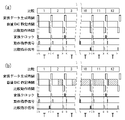
- the [capacitive DAC static time] assigned to the potential generation operation by the capacitance DAC2 is the static time for each bit. , Assuming the maximum case, the same time T is set from the upper bit to the lower bit.
- FIG. 8 shows an example with a resolution of 12 bits.
- statically determinate time in the capacitance DAC2 is not uniform with respect to the bit to be switched, and tends to become shorter as the bit becomes lower, so that the wasted time shown by the diagonal line in FIG. 8B [capacity]. It is assigned as [DAC static time], which hinders the speeding up of the A / D conversion circuit 1.
- the present invention has been made in view of such problems, and an object thereof is to provide an A / D conversion circuit capable of realizing high speed by eliminating an excessive allocation of [capacity DAC statically determinate time]. There is a point to do.
- the A / D conversion circuit according to the present invention is configured as follows in order to achieve the above object.
- the A / D conversion circuit according to the present invention digitally converts an analog input by repeating a conversion data generation operation by a conversion data generator, a potential generation operation by a capacitive DAC, and a comparison operation by a comparator for a resolution bit. It is a sequential comparison type analog-to-digital conversion circuit that converts to a value, and the potential generated by the capacitive DAC is statically determined based on the charge / discharge time to the capacitive element having the same characteristics as the capacitance used in the capacitive DAC. It is characterized by comprising a comparator operation signal generation circuit that predicts a time and generates a comparator operation signal that causes the comparator to start the comparison operation.
- the A / D conversion circuit of the present invention can predict the truly required [capacitive DAC statically determinate time] by using the capacitive element 51 having the same characteristics as the capacitance used in the capacitive DAC2, and can predict an excessive [capacity DAC]. It has the effect of eliminating the allocation of [statically determinate time] and achieving high speed.
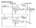
- FIG. 1st Embodiment of the A / D conversion circuit which concerns on this invention. It is an operation explanatory diagram of the A / D conversion circuit shown in FIG. It is a figure which shows the 1st modification of the comparator operation signal generation circuit shown in FIG. It is a figure which shows the 2nd modification of the comparator operation signal generation circuit shown in FIG. It is a figure which shows the 3rd modification of the comparator operation signal generation circuit shown in FIG. It is a figure which shows the 4th modification of the comparator operation signal generation circuit shown in FIG. It is a figure which shows the structure of the conventional A / D conversion circuit. It is operation
- the A / D conversion circuit 10 of the present embodiment is a sequential comparison type, and referring to FIG. 1, a capacitive DAC 2, a comparator 3, a conversion data generator 40, and a comparator operation signal generation circuit 5 are used. I have.
- the A / D conversion circuit 10 compares the potential generated by the capacitance DAC2 based on the analog input potential with the comparator 3, feeds back the result to the conversion data generator 40, and transmits the approximate data candidate to the capacitance DAC2. This repetition is repeated for the resolution bit (n bits: n times) to obtain a digital conversion value.
- each of the capacitances C 0 to C (n-1) weighted as 2 (n- 1) with respect to the switching bit (n-1) is connected to the common comparison wiring 21. It is connected and the potential of the comparison wiring 21 is compared with the reference potential Vref by the comparator 3.
- Each other end of the capacitances C 0 to C (n-1) has an analog input (potential), a reference potential (High), and a reference potential (Low) via switches 220 to 22 (n-1) , respectively. And, any one of them is selected and connected.
- the capacitance C a is a dummy capacitor having a capacitance C 0 capacitance value, one end of the capacitance C a is connected to the comparison wiring 21, and the other end is connected to the analog input (potential) via the switch 22 a . , Reference potential (Low), and any one is selected and connected.
- any one of the capacitances C 0 to C (n-1) is connected to the reference potential (High) or the reference potential (Low) via the switches 220 to 22 (n-1) according to the bit to be switched. By doing so, you will reach the target level. Therefore, the static time is the time for charging the capacitances C 0 to C (n-1) to the reference potential (High) or the time for discharging to the reference potential (Low) via the switches 220 to 22 (n-1) . Become.
- the comparator operation signal generation circuit 5 predicts the time when the potential generated by the capacitance DAC 2 is statically determinate based on the conversion data generated by the conversion data generator 40, and causes the comparator 3 to start the comparison operation. To generate.
- the capacitance element 51 having the same characteristics as the capacitances C 0 to C (n-1) used in the capacitance DAC 2, the charge / discharge switch 52 for the capacitance element 51, and the capacitance element 51 are charged. It includes a potential changeover switch 53 for switching the potential to be applied, and an inverter circuit 54 for outputting a comparison start signal when the potential of the capacitive element 51 falls below the threshold potential.
- the charge / discharge switch 52 includes a charge switch 521 that connects the other end of the capacitance element 51 to one end of the potential changeover switch 53, and a discharge switch 522 that connects the other end of the capacitance element 51 to the ground terminal, and generates conversion data.
- the on / off of the charge switch 521 and the discharge switch 522 is controlled by the charge / discharge instruction signal from the device 40.
- the charge switch 521 when the charge / discharge instruction signal is Low, the charge switch 521 is controlled to be on and the discharge switch 522 is turned off, and when the charge / discharge instruction signal is High, the charge switch 521 is turned off and the discharge switch 522 is controlled to be on.
- the discharge switch 522 is on, which is equivalent to the on-resistance of the switches 220 to 22 (n-1) when the capacitances C 0 to C (n-1) are connected to the reference potential (High) or the reference potential (Low). Those with resistance are used.
- the charge switch 521 has an on-resistance lower than that of the discharge switch 522, and is compatible with quick charging.
- the potential changeover switch 53 is a connection switch 531 (n ) having a resolution bit that connects the other end of the capacitive element 51 and n injection potentials (n-1) to an injection potential (0) for the resolution bit. -1) The injection potential (n-1) to 531 (0) is provided, and the injection potential for injecting (charging) the electric charge into the capacitive element 51 by the potential switching instruction signal from the conversion data generator 40 is applied. Select from and switch.
- the injection potentials (n-1) to the injection potentials (0) are potentials for simulating the amount of electric charge injected or discharged into the capacitive DAC2, and reach the threshold potential of the inverter circuit 54 when discharged from the capacitive element 51.
- the time until is set to be the maximum value of the statically determinate time (reference potential by charging) for each of the highest to lowest bits.
- the conversion data generator 40 instructs the potential changeover switch 53 of the comparator operation signal generation circuit 5 to connect to the injection potential (n-1) corresponding to the highest bit by the potential changeover instruction signal, and also indicates the charge / discharge instruction signal. Is set to Low to charge the capacitance element 51 to the injection potential (n-1), and when the conversion start signal is input, the conversion data generation operation is started.
- the conversion data generator 40 outputs the capacitance DAC input value of the highest bit to the capacitance DAC 2 at the timing of the operation start signal generated after a predetermined time from the conversion start signal (after the conversion data generation operation is completed).
- the comparator operation signal generation circuit 5 is instructed to discharge from the capacitive element 51 by shifting the charge / discharge instruction signal to High.
- the capacitance DAC2 generates a potential for determining the highest bit by the potential generation operation, and in the comparator operation signal generation circuit 5, the injection potential (n-1) charged in the capacitance element 51 by discharge is the inverter circuit. When it falls below the threshold potential, the comparison start signal is output to the comparator 3 and the conversion data generator 40. That is, the comparator operation signal generation circuit 5 is different for each bit to be switched by using the capacitance element 51 having the same characteristics as the capacitance used in the capacitance DAC2 and the injection potential (0) to the injection potential (n-1).
- the statically determinate time of the capacitance DAC2 is predicted, and the comparison start signal is output at the timing when the statically determinate time ends.
- the comparator 3 Upon input to the comparison start signal, the comparator 3 compares the potential generated by the potential generation operation of the capacitance DAC2 with the reference potential, and outputs the comparison result to the conversion data generator 40. Further, by inputting to the comparison start signal, the conversion data generator 40 instructs the potential changeover switch 53 of the comparer operation signal generation circuit 5 to connect to the injection potential (n-2) corresponding to the next bit by the changeover instruction signal. Then, the charge / discharge instruction signal is set to Low to charge the capacitance element 51. Further, the conversion data generator 40 is the conversion data D (n ) of the most significant bit based on the comparison result of the comparator 3 at the timing of the conversion signal generated after a predetermined time from the comparison start signal (after the conversion comparison operation is completed). -1) Start the conversion data generation operation to generate.
- the conversion data generator 40 is the conversion data of the highest bit (comparison result of the comparer 3) at the timing of the operation start signal generated after a predetermined time from the conversion start signal (after the conversion data generation operation is completed).
- the charging / discharging instruction signal is changed to High in the comparator operation signal generation circuit 5 to instruct the discharge from the capacitance element 51.
- the capacitive DAC 2 generates a potential for determining the next bit by the potential generation operation, and the comparator operation signal generation circuit 5 generates a comparison start signal when the potential of the capacitive element 51 falls below the threshold potential of the inverter circuit 54 due to discharge. Is output to the comparator 3 and the conversion data generator 40.
- the comparator 3 Upon input to the comparison start signal, the comparator 3 compares the potential generated by the potential generation operation of the capacitance DAC2 with the reference potential, and outputs the comparison result to the conversion data generator 40. Further, by inputting to the comparison start signal, the conversion data generator 40 instructs the potential changeover switch 53 of the comparer operation signal generation circuit 5 to connect to the injection potential (n-3) corresponding to the next bit by the changeover instruction signal. Then, the charge / discharge instruction signal is set to Low to charge the capacitance element 51. Further, the conversion data generator 40 has the conversion data D (n ) of the next bit based on the comparison result of the comparator 3 at the timing of the conversion signal generated after a predetermined time from the comparison start signal (after the conversion comparison operation ends). -Start the conversion data generation operation to generate -2) .
- the above operation is repeated until the conversion data of the most significant bit is generated by repeating the comparison of the resolution bits (12 bits), and the conversion data generator 40 performs the conversion data D (n-1) to D (0 ). ) Is output as a conversion value.
- the [capacitated DAC static time] T 1 to T 12 assigned to the potential generation operation by the capacitive DAC 2 are set to be shorter from the upper bit to the lower bit according to the static time for each bit, and the speed is increased. Can be realized. It should be noted that the lower the bit, the shorter the statically determinate time, but the smaller the decrease. Therefore, the plurality of preset lower bits may correspond at the same injection potential.
- the comparator operation signal generation circuit 5a which is the first modification, predicts the statically determinate time of the capacitance DAC2, which is different for each bit to be switched, and outputs the comparison start signal at the timing when the statically determinate time ends.
- the generation circuit 50 (n-1) to the generation circuit 50 (0) include a capacitance element 51, a charge / discharge switch 52, and an inverter circuit 54, respectively, and one end of each capacitance element 51 is connected to a ground terminal. The other end is connected to the input terminal of the inverter circuit 54 and one end of the charge / discharge switch 52.
- the charge / discharge switch 52 of the generation circuit 50 (n-1) to the generation circuit 50 (0) is a charge switch 521 that connects the other end of the capacitance element 51 to the injection potential (n-1) to the injection potential (0), respectively.
- a discharge switch 522 that connects the other end of the capacitance element 51 to the ground terminal is provided, and on / off of the charge switch 521 and the discharge switch 522 is controlled by a charge / discharge instruction signal from the conversion data generator 40.
- the output changeover switch 55 includes n connection switches 551 (n - 1) to 551 (0) for the resolution bit, and is generated by the output changeover instruction signal from the conversion data generator 40. From the generation circuit 50 (0) , the one that outputs the comparison start signal is selected and switched.
- the output changeover switch 55 is used. It can be omitted.
- the comparator operation signal generation circuit 5b which is a second modification, is a generation circuit that generates a timing for outputting a comparison start signal by using a capacitance element 51 having the same characteristics as the capacitance used in the capacitance DAC2, referring to FIG. 501 is connected in series (series) in N stages and includes an output changeover switch 55 for selecting which comparison start signal is to be output to the comparator 3.
- the N generation circuits 501 include a capacitance element 51, a charge / discharge switch 52, and an inverter circuit 54, respectively, and the comparison start signal output from the inverter circuit 54 is a discharge instruction signal to the next stage charge / discharge switch 52. Connected to be entered as.
- the charge / discharge switch 52 includes a charge switch 521 that connects the other end of the capacitance element 51 to the injection potential, and a discharge switch 522 that connects the other end of the capacitance element 51 to the ground terminal, and is a conversion data generator 40.
- the charge switch 521 is turned on, the discharge switch 522 is turned off, and the electric charge is injected into the capacitive element 51 according to the charge instruction signal from.
- the first -stage generation circuit 501 When a charge instruction signal is input from the conversion data generator 40 to the first -stage generation circuit 501 in a state where electric charges are injected into the capacitance elements 51 of all stages, the first -stage generation circuit 501 The charge switch 521 is turned off, the discharge switch 522 is turned on, and the discharge from the capacitive element 51 is started. When the potential of the capacitive element 51 falls below the threshold potential of the inverter circuit 54 due to discharge, a comparison start signal is output and input as a discharge instruction signal to the charge / discharge switch 52 in the next stage.
- the statically determinate time of the capacitance DAC2 which is different for each bit to be switched, is predicted. Then, the comparison start signal can be output to the comparator 3 at the timing when the statically determinate time ends.
- the comparator operation signal generation circuit 5c which is a third modification, is a generation circuit that generates a timing for outputting a comparison start signal by using a capacitance element 51 having the same characteristics as the capacitance used in the capacitance DAC2, referring to FIG.
- the 501 is connected in two stages and includes an output selector switch 55 for selecting which comparison start signal is to be output to the comparator 3.
- the two-stage generation circuit 501 includes a capacitance element 51, a charge / discharge switch 52, and an inverter circuit 54, respectively, and the comparison start signal output from the inverter circuit 54 is a discharge instruction signal to the charge / discharge switch 52 in the other stage. Connected to be entered as.
- the charge / discharge switch 52 includes a charge switch 521 that connects the other end of the capacitance element 51 to the injection potential, and a discharge switch 522 that connects the other end of the capacitance element 51 to the ground terminal, and is a conversion data generator 40.
- the charge switch 521 is turned on, the discharge switch 522 is turned off, and the electric charge is injected into the capacitive element 51 according to the charge instruction signal from.
- the first -stage generation circuit 501 When a discharge instruction signal is input from the conversion data generator 40 to the first -stage generation circuit 501 in a state where electric charges are injected into the capacitance elements 51 of all stages, the first -stage generation circuit 501 is charged. The switch 521 is turned off, the discharge switch 522 is turned on, and discharge from the capacitance element 51 is started. When the potential of the capacitance element 51 falls below the threshold potential of the inverter circuit 54 due to the discharge, a comparison start signal is output. The comparison start signal output from the first -stage generation circuit 501 is input to the second-stage charge / discharge switch 52 as a discharge instruction signal, and is also input to the conversion data generator 40 as a completion signal.
- the charge switch 521 is turned off, the discharge switch 522 is turned on, and discharge from the capacitive element 51 is started, and the conversion data generator 40 generates the first stage.
- a charging instruction signal is output to the circuit 501 to start charging the capacitive element 51.
- a comparison start signal is output and input to the first-stage charge / discharge switch 52 as a discharge instruction signal.
- it is input to the conversion data generator 40 as a completion signal.
- the comparison start signal is output at the time quantized by repetition, and the conversion data generator 40 outputs the output changeover instruction signal to the output changeover switch 55 at a desired timing by counting the input completion signal.
- One of the connection switches 551 1 and 551 2 of the output selector switch 55 is turned on, and the comparison start signal is output to the comparator 3.
- the two-stage generation circuit 501 can predict the statically determinate time of the different capacitance DAC 2 for each bit to be switched, and output the comparison start signal to the comparator 3 at the timing when the statically determinate time ends.
- the comparator operation signal generation circuit 5d which is a fourth modification, starts comparison when the potentials of the capacitive element 51, the charge / discharge switch 52a, the inverter circuit 54, and the capacitive element 51 exceed the threshold potential.
- a generation circuit 502 including a buffer circuit 56 for outputting a signal, and an output selector switch 55a for selecting which of the inverter circuit 54 and the buffer circuit 56 the comparison start signal is to be output to the comparator 3 are provided. There is.
- the charge / discharge switch 52a includes a charge switch 521a that connects the other end of the capacitance element 51 to the injection potential, and a discharge switch 522 that connects the other end of the capacitance element 51 to the ground terminal, and operates on the capacitance DAC2.
- the charge switch 521a is turned on and the discharge switch 522 is turned off by the charge instruction signal output from the conversion data generator 40 at the same time as the instruction signal, and the electric charge is injected into the capacitive element 51.
- the charge switch 521a and the discharge switch 522 have the on-resistance of the switches 220 to 22 (n-1) when the capacitances C 0 to C (n-1) are connected to the reference potential (High) or the reference potential (Low). , Those having the same on-resistance are used.
- the comparison start signal is output from the buffer circuit 56.
- the comparison start signal output from the buffer circuit 56 is input to the charge / discharge switch 52a as a discharge instruction signal, and is also input to the conversion data generator 40 as a completion signal.
- a discharge instruction signal is input from the buffer circuit 56, the charge switch 521a is turned off, the discharge switch 522 is turned on, and discharge from the capacitance element 51 is started.
- a comparison start signal is output from the inverter circuit 54.
- the comparison start signal output from the inverter circuit 54 is input to the charge / discharge switch 52a as a charge instruction signal, and is also input to the conversion data generator 40 as a completion signal.
- the comparison start signal is output at the time quantized by repetition, and the conversion data generator 40 outputs the output switching instruction signal to the output changeover switch 55a at a desired timing by counting the input completion signal.
- one generation circuit 502 can predict the statically determinate time of the capacitance DAC2 different for each bit to be switched, and output the comparison start signal to the comparator 3 at the timing when the statically determinate time ends.
- the analog input is performed by repeating the conversion data generation operation by the conversion data generator 40, the potential generation operation by the capacitive DAC 2, and the comparison operation by the comparator 3 for the resolution bit.
- It is a sequential comparison type A / D conversion circuit 10 that converts to a digital conversion value, and is based on the charge / discharge time to the capacitance element 51 having the same characteristics as the capacitances C0 to C (n-1) used in the capacitance DAC2.
- the comparator operation signal generation circuit 5 for predicting the time when the potential generated by the capacitance DAC 2 is settled and generating the comparator operation signal for causing the comparator 3 to start the comparison operation is provided.
- the comparator operation signal generation circuits 5 and 5a are bits to be switched based on the discharge time of each of the capacitive elements 51 charged at the plurality of injection potentials (n-1) to (0).
- the statically determinate time of the different capacitance DAC2 is predicted for each.
- the comparator operation signal generation circuits 5b and 5c predict the statically determinate time of the capacitance DAC2, which is different for each bit to be switched, by repeating the discharge time of the capacitance element 51 charged at the injection potential.
- [capacity DAC static time] can be predicted without preparing a plurality of injection potentials.
- the capacitance element 51 is discharged via the discharge switch 522, and the discharge switch 522 has a capacitance C 0 to C (n-1) and a reference potential (High) or a reference potential (Low). It has the same on-resistance as the on-resistance of switches 220 to 22 (n-1) at the time of connection. With this configuration, the statically determinate time can be predicted more accurately.
- the comparator operation signal generation circuit 5d is switched for each bit by repeating the charging time for charging the capacitive element 51 at the injection potential and the discharging time for the capacitive element 51 charged at the injection potential.
- Each statically determinate time of different capacitance DAC2 is predicted. With this configuration, the [capacitive DAC statically determinate time] can be predicted by using only one capacitive element 51.
- the capacitance element 51 is charged and discharged via the charging switch 521a and the discharging switch 522, respectively, and the charging switch 521a and the discharging switch 522 have capacitances C 0 to C (n-1) and a reference potential. It has an on-resistance equivalent to the on-resistance of the switches 220 to 22 (n-1) at the time of connection with (High) or a reference potential (Low). With this configuration, the statically determinate time can be predicted more accurately.
Landscapes
- Engineering & Computer Science (AREA)
- Theoretical Computer Science (AREA)
- Power Engineering (AREA)
- Analogue/Digital Conversion (AREA)
Priority Applications (4)
| Application Number | Priority Date | Filing Date | Title |
|---|---|---|---|
| PCT/JP2020/042169 WO2022102035A1 (ja) | 2020-11-12 | 2020-11-12 | アナログデジタル変換回路 |
| JP2021576414A JP7551061B2 (ja) | 2020-11-12 | 2020-11-12 | アナログデジタル変換回路 |
| CN202080025706.7A CN114766080B (zh) | 2020-11-12 | 2020-11-12 | 模拟/数字转换电路 |
| US17/488,367 US11757460B2 (en) | 2020-11-12 | 2021-09-29 | Analog-to-digital converter |
Applications Claiming Priority (1)
| Application Number | Priority Date | Filing Date | Title |
|---|---|---|---|
| PCT/JP2020/042169 WO2022102035A1 (ja) | 2020-11-12 | 2020-11-12 | アナログデジタル変換回路 |
Related Child Applications (1)
| Application Number | Title | Priority Date | Filing Date |
|---|---|---|---|
| US17/488,367 Continuation US11757460B2 (en) | 2020-11-12 | 2021-09-29 | Analog-to-digital converter |
Publications (1)
| Publication Number | Publication Date |
|---|---|
| WO2022102035A1 true WO2022102035A1 (ja) | 2022-05-19 |
Family
ID=81453682
Family Applications (1)
| Application Number | Title | Priority Date | Filing Date |
|---|---|---|---|
| PCT/JP2020/042169 Ceased WO2022102035A1 (ja) | 2020-11-12 | 2020-11-12 | アナログデジタル変換回路 |
Country Status (4)
| Country | Link |
|---|---|
| US (1) | US11757460B2 (https=) |
| JP (1) | JP7551061B2 (https=) |
| CN (1) | CN114766080B (https=) |
| WO (1) | WO2022102035A1 (https=) |
Families Citing this family (2)
| Publication number | Priority date | Publication date | Assignee | Title |
|---|---|---|---|---|
| US20240348260A1 (en) * | 2023-04-14 | 2024-10-17 | Skyworks Solutions, Inc. | Capacitive digital-to-analog converters with shaped output current |
| CN120357902B (zh) * | 2025-06-23 | 2025-09-02 | 灿芯半导体(苏州)有限公司 | 一种pvt稳定的逐次逼近型模数转换器 |
Citations (7)
| Publication number | Priority date | Publication date | Assignee | Title |
|---|---|---|---|---|
| JPS6198022A (ja) * | 1984-10-19 | 1986-05-16 | Matsushita Electric Ind Co Ltd | 遂次比較方式アナログデイジタル変換装置 |
| JPH05122076A (ja) * | 1991-10-25 | 1993-05-18 | Nec Corp | アナログデイジタル変換器 |
| JPH08116258A (ja) * | 1994-10-18 | 1996-05-07 | Toshiba Corp | アナログデジタル変換回路 |
| JP2001267925A (ja) * | 2000-03-17 | 2001-09-28 | Matsushita Electric Ind Co Ltd | 逐次比較型ad変換器 |
| WO2010010661A1 (ja) * | 2008-07-21 | 2010-01-28 | 株式会社アドバンテスト | Ad変換装置 |
| JP2010245927A (ja) * | 2009-04-08 | 2010-10-28 | Mitsumi Electric Co Ltd | 逐次比較型ad変換回路 |
| JP2011199443A (ja) * | 2010-03-18 | 2011-10-06 | Fujitsu Semiconductor Ltd | 逐次比較型a/dコンバータ、および逐次比較型a/dコンバータの比較時間検出方法 |
Family Cites Families (20)
| Publication number | Priority date | Publication date | Assignee | Title |
|---|---|---|---|---|
| JPS5115363A (ja) | 1974-07-29 | 1976-02-06 | Hitachi Ltd | Anaroguudejitaruhenkanki |
| JPS62133821A (ja) | 1985-12-05 | 1987-06-17 | Matsushita Electric Ind Co Ltd | アナログ・デジタル変換器 |
| JP2006173807A (ja) * | 2004-12-13 | 2006-06-29 | Sanyo Electric Co Ltd | アナログデジタル変換器 |
| JP2010063055A (ja) * | 2008-09-08 | 2010-03-18 | Sony Corp | 逐次比較型a/d変換器、逐次比較型a/d変換器の制御方法、固体撮像装置および撮像装置 |
| JP5482158B2 (ja) * | 2009-12-04 | 2014-04-23 | ヤマハ株式会社 | 逐次比較a/d変換器 |
| US8786483B1 (en) * | 2013-03-14 | 2014-07-22 | Analog Devices Technology | Use of a DLL to optimize an ADC performance |
| US9041584B2 (en) * | 2013-09-03 | 2015-05-26 | Silicon Laboratories Inc. | Dual-path comparator and method |
| US8957802B1 (en) * | 2013-09-13 | 2015-02-17 | Cadence Design Systems, Inc. | Metastability error detection and correction system and method for successive approximation analog-to-digital converters |
| KR101524982B1 (ko) * | 2014-07-31 | 2015-06-03 | 중앙대학교 산학협력단 | 비동기식 연속 근사 레지스터 아날로그 디지털 변환기 및 그에 포함되는 내부 클럭 발생기 |
| KR102276893B1 (ko) * | 2015-09-24 | 2021-07-12 | 삼성전자주식회사 | 축차 근사 레지스터 아날로그 디지털 변환기와 이를 포함하는 반도체 장치 |
| US9614540B1 (en) * | 2015-11-06 | 2017-04-04 | International Business Machines Corporation | Asynchronously clocked successive approximation register analog-to-digital converter |
| US9621179B1 (en) * | 2016-03-11 | 2017-04-11 | Applied Micro Circuits Corporation | Metastability error reduction in asynchronous successive approximation analog to digital converter |
| RU2695493C2 (ru) * | 2016-05-31 | 2019-07-23 | Общество с ограниченной ответственностью "Научно-производственное предприятие Тачскрин технологии" | Проекционно-ёмкостная сенсорная панель и способ её изготовления |
| US9893740B1 (en) * | 2017-01-13 | 2018-02-13 | Semiconductor Components Industries, Llc | Methods and apparatus for an analog-to-digital converter |
| JP6899287B2 (ja) * | 2017-09-01 | 2021-07-07 | 株式会社日立製作所 | 逐次比較型アナログデジタル変換器 |
| CN207427126U (zh) * | 2017-09-28 | 2018-05-29 | 成都启英泰伦科技有限公司 | 一种提高模数转换器转换速度的电路 |
| US10454492B1 (en) * | 2018-06-19 | 2019-10-22 | Analog Devices, Inc. | Analog-to-digital converter speed calibration techniques |
| US10291251B1 (en) * | 2018-09-21 | 2019-05-14 | Semiconductor Components Industries, Llc | Imaging systems with sub-radix-2 charge sharing successive approximation register (SAR) analog-to-digital converters |
| CN114759926A (zh) * | 2021-01-08 | 2022-07-15 | 博通集成电路(上海)股份有限公司 | 逐次逼近寄存器模数转换器电路 |
| US11387838B1 (en) * | 2021-03-19 | 2022-07-12 | Microsoft Technology Licensing, Llc | SAR analog-to-digital converter calibration |
-
2020
- 2020-11-12 JP JP2021576414A patent/JP7551061B2/ja active Active
- 2020-11-12 CN CN202080025706.7A patent/CN114766080B/zh active Active
- 2020-11-12 WO PCT/JP2020/042169 patent/WO2022102035A1/ja not_active Ceased
-
2021
- 2021-09-29 US US17/488,367 patent/US11757460B2/en active Active
Patent Citations (7)
| Publication number | Priority date | Publication date | Assignee | Title |
|---|---|---|---|---|
| JPS6198022A (ja) * | 1984-10-19 | 1986-05-16 | Matsushita Electric Ind Co Ltd | 遂次比較方式アナログデイジタル変換装置 |
| JPH05122076A (ja) * | 1991-10-25 | 1993-05-18 | Nec Corp | アナログデイジタル変換器 |
| JPH08116258A (ja) * | 1994-10-18 | 1996-05-07 | Toshiba Corp | アナログデジタル変換回路 |
| JP2001267925A (ja) * | 2000-03-17 | 2001-09-28 | Matsushita Electric Ind Co Ltd | 逐次比較型ad変換器 |
| WO2010010661A1 (ja) * | 2008-07-21 | 2010-01-28 | 株式会社アドバンテスト | Ad変換装置 |
| JP2010245927A (ja) * | 2009-04-08 | 2010-10-28 | Mitsumi Electric Co Ltd | 逐次比較型ad変換回路 |
| JP2011199443A (ja) * | 2010-03-18 | 2011-10-06 | Fujitsu Semiconductor Ltd | 逐次比較型a/dコンバータ、および逐次比較型a/dコンバータの比較時間検出方法 |
Also Published As
| Publication number | Publication date |
|---|---|
| JP7551061B2 (ja) | 2024-09-17 |
| CN114766080A (zh) | 2022-07-19 |
| US20220149852A1 (en) | 2022-05-12 |
| US11757460B2 (en) | 2023-09-12 |
| JPWO2022102035A1 (https=) | 2022-05-19 |
| CN114766080B (zh) | 2025-10-28 |
Similar Documents
| Publication | Publication Date | Title |
|---|---|---|
| US20100060500A1 (en) | Analog/Digital Converter Assembly and Corresponding Method | |
| US10727857B2 (en) | Successive approximation register (SAR) analog to digital converter (ADC) with switchable reference voltage | |
| WO2022102035A1 (ja) | アナログデジタル変換回路 | |
| JP2751186B2 (ja) | ディジタル・アナログ変換回路 | |
| EP0289081A1 (en) | Digital-to-analog converter | |
| US11342931B2 (en) | Reference voltage controlling circuit and analog-to-digital converter | |
| KR100690434B1 (ko) | 디지털 아날로그 변환기, 데이터 라인 드라이버,디스플레이 장치, 및 그 방법 | |
| US7652607B2 (en) | Digital to analogue converters | |
| JP3300230B2 (ja) | 線形型デイジタルアナログ変換器及びその駆動方法 | |
| EP0681372B1 (en) | Digital-to-analog conversion circuit and analog-to-digital conversion device using the circuit | |
| US6927723B2 (en) | A/D converter and A/D conversion method | |
| JPS6016135B2 (ja) | 変換器 | |
| US5298902A (en) | Analog-to-digital converter employing multiple parallel switching capacitor circuits | |
| US8957804B2 (en) | Successive approximation A/D converter | |
| JP2000101432A (ja) | アナログ信号をデジタル表示に変換する方法 | |
| JP3130007B2 (ja) | 逐次比較型a/dコンバータ回路 | |
| JP2609239B2 (ja) | A/dコンバータ及びa/dコンバート方法 | |
| JP2002314419A (ja) | A/d変換回路 | |
| JPH06268522A (ja) | 容量列形da変換回路 | |
| JP2009188736A (ja) | Ad変換器 | |
| KR100207508B1 (ko) | 디지털 아날로그 컨버터 | |
| US12273119B2 (en) | Analog-to-digital converter circuit and semiconductor integrated circuit | |
| US6222475B1 (en) | Three-step converter | |
| KR20070048540A (ko) | 저항 스트링 컨버터와 커패시터 컨버터를 결합하는디지털-아날로그 컨버팅 드라이버 및 디지털-아날로그컨버팅 방법 | |
| CN117335804A (zh) | 一种逐次逼近型模数转换器及终端设备 |
Legal Events
| Date | Code | Title | Description |
|---|---|---|---|
| ENP | Entry into the national phase |
Ref document number: 2021576414 Country of ref document: JP Kind code of ref document: A |
|
| 121 | Ep: the epo has been informed by wipo that ep was designated in this application |
Ref document number: 20961563 Country of ref document: EP Kind code of ref document: A1 |
|
| NENP | Non-entry into the national phase |
Ref country code: DE |
|
| 122 | Ep: pct application non-entry in european phase |
Ref document number: 20961563 Country of ref document: EP Kind code of ref document: A1 |
|
| WWG | Wipo information: grant in national office |
Ref document number: 202080025706.7 Country of ref document: CN |