WO2022054327A1 - 半導体装置 - Google Patents
半導体装置 Download PDFInfo
- Publication number
- WO2022054327A1 WO2022054327A1 PCT/JP2021/014967 JP2021014967W WO2022054327A1 WO 2022054327 A1 WO2022054327 A1 WO 2022054327A1 JP 2021014967 W JP2021014967 W JP 2021014967W WO 2022054327 A1 WO2022054327 A1 WO 2022054327A1
- Authority
- WO
- WIPO (PCT)
- Prior art keywords
- tungsten
- hole
- region
- pad
- gate
- Prior art date
- Legal status (The legal status is an assumption and is not a legal conclusion. Google has not performed a legal analysis and makes no representation as to the accuracy of the status listed.)
- Ceased
Links
Images


Classifications
-
- H—ELECTRICITY
- H10—SEMICONDUCTOR DEVICES; ELECTRIC SOLID-STATE DEVICES NOT OTHERWISE PROVIDED FOR
- H10D—INORGANIC ELECTRIC SEMICONDUCTOR DEVICES
- H10D64/00—Electrodes of devices having potential barriers
- H10D64/20—Electrodes characterised by their shapes, relative sizes or dispositions
- H10D64/23—Electrodes carrying the current to be rectified, amplified, oscillated or switched, e.g. sources, drains, anodes or cathodes
- H10D64/231—Emitter or collector electrodes for bipolar transistors
-
- H—ELECTRICITY
- H10—SEMICONDUCTOR DEVICES; ELECTRIC SOLID-STATE DEVICES NOT OTHERWISE PROVIDED FOR
- H10D—INORGANIC ELECTRIC SEMICONDUCTOR DEVICES
- H10D64/00—Electrodes of devices having potential barriers
- H10D64/20—Electrodes characterised by their shapes, relative sizes or dispositions
- H10D64/27—Electrodes not carrying the current to be rectified, amplified, oscillated or switched, e.g. gates
- H10D64/311—Gate electrodes for field-effect devices
- H10D64/411—Gate electrodes for field-effect devices for FETs
- H10D64/511—Gate electrodes for field-effect devices for FETs for IGFETs
- H10D64/517—Gate electrodes for field-effect devices for FETs for IGFETs characterised by the conducting layers
- H10D64/519—Gate electrodes for field-effect devices for FETs for IGFETs characterised by the conducting layers characterised by their top-view geometrical layouts
-
- H—ELECTRICITY
- H10—SEMICONDUCTOR DEVICES; ELECTRIC SOLID-STATE DEVICES NOT OTHERWISE PROVIDED FOR
- H10D—INORGANIC ELECTRIC SEMICONDUCTOR DEVICES
- H10D64/00—Electrodes of devices having potential barriers
- H10D64/20—Electrodes characterised by their shapes, relative sizes or dispositions
- H10D64/23—Electrodes carrying the current to be rectified, amplified, oscillated or switched, e.g. sources, drains, anodes or cathodes
- H10D64/232—Emitter electrodes for IGBTs
-
- H—ELECTRICITY
- H10—SEMICONDUCTOR DEVICES; ELECTRIC SOLID-STATE DEVICES NOT OTHERWISE PROVIDED FOR
- H10P—GENERIC PROCESSES OR APPARATUS FOR THE MANUFACTURE OR TREATMENT OF DEVICES COVERED BY CLASS H10
- H10P74/00—Testing or measuring during manufacture or treatment of wafers, substrates or devices
- H10P74/27—Structural arrangements therefor
- H10P74/273—Interconnections for measuring or testing, e.g. probe pads
-
- H—ELECTRICITY
- H10—SEMICONDUCTOR DEVICES; ELECTRIC SOLID-STATE DEVICES NOT OTHERWISE PROVIDED FOR
- H10W—GENERIC PACKAGES, INTERCONNECTIONS, CONNECTORS OR OTHER CONSTRUCTIONAL DETAILS OF DEVICES COVERED BY CLASS H10
- H10W20/00—Interconnections in chips, wafers or substrates
- H10W20/01—Manufacture or treatment
- H10W20/031—Manufacture or treatment of conductive parts of the interconnections
- H10W20/032—Manufacture or treatment of conductive parts of the interconnections of conductive barrier, adhesion or liner layers
- H10W20/033—Manufacture or treatment of conductive parts of the interconnections of conductive barrier, adhesion or liner layers in openings in dielectrics
-
- H—ELECTRICITY
- H10—SEMICONDUCTOR DEVICES; ELECTRIC SOLID-STATE DEVICES NOT OTHERWISE PROVIDED FOR
- H10W—GENERIC PACKAGES, INTERCONNECTIONS, CONNECTORS OR OTHER CONSTRUCTIONAL DETAILS OF DEVICES COVERED BY CLASS H10
- H10W20/00—Interconnections in chips, wafers or substrates
- H10W20/01—Manufacture or treatment
- H10W20/071—Manufacture or treatment of dielectric parts thereof
- H10W20/081—Manufacture or treatment of dielectric parts thereof by forming openings in the dielectric parts
- H10W20/089—Manufacture or treatment of dielectric parts thereof by forming openings in the dielectric parts using processes for implementing desired shapes or dispositions of the openings, e.g. double patterning
-
- H—ELECTRICITY
- H10—SEMICONDUCTOR DEVICES; ELECTRIC SOLID-STATE DEVICES NOT OTHERWISE PROVIDED FOR
- H10W—GENERIC PACKAGES, INTERCONNECTIONS, CONNECTORS OR OTHER CONSTRUCTIONAL DETAILS OF DEVICES COVERED BY CLASS H10
- H10W20/00—Interconnections in chips, wafers or substrates
- H10W20/40—Interconnections external to wafers or substrates, e.g. back-end-of-line [BEOL] metallisations or vias connecting to gate electrodes
- H10W20/41—Interconnections external to wafers or substrates, e.g. back-end-of-line [BEOL] metallisations or vias connecting to gate electrodes characterised by their conductive parts
- H10W20/425—Barrier, adhesion or liner layers
-
- H—ELECTRICITY
- H10—SEMICONDUCTOR DEVICES; ELECTRIC SOLID-STATE DEVICES NOT OTHERWISE PROVIDED FOR
- H10W—GENERIC PACKAGES, INTERCONNECTIONS, CONNECTORS OR OTHER CONSTRUCTIONAL DETAILS OF DEVICES COVERED BY CLASS H10
- H10W20/00—Interconnections in chips, wafers or substrates
- H10W20/40—Interconnections external to wafers or substrates, e.g. back-end-of-line [BEOL] metallisations or vias connecting to gate electrodes
- H10W20/41—Interconnections external to wafers or substrates, e.g. back-end-of-line [BEOL] metallisations or vias connecting to gate electrodes characterised by their conductive parts
- H10W20/43—Layouts of interconnections
-
- H—ELECTRICITY
- H10—SEMICONDUCTOR DEVICES; ELECTRIC SOLID-STATE DEVICES NOT OTHERWISE PROVIDED FOR
- H10D—INORGANIC ELECTRIC SEMICONDUCTOR DEVICES
- H10D12/00—Bipolar devices controlled by the field effect, e.g. insulated-gate bipolar transistors [IGBT]
- H10D12/411—Insulated-gate bipolar transistors [IGBT]
- H10D12/441—Vertical IGBTs
- H10D12/461—Vertical IGBTs having non-planar surfaces, e.g. having trenches, recesses or pillars in the surfaces of the emitter, base or collector regions
- H10D12/481—Vertical IGBTs having non-planar surfaces, e.g. having trenches, recesses or pillars in the surfaces of the emitter, base or collector regions having gate structures on slanted surfaces, on vertical surfaces, or in grooves, e.g. trench gate IGBTs
-
- H—ELECTRICITY
- H10—SEMICONDUCTOR DEVICES; ELECTRIC SOLID-STATE DEVICES NOT OTHERWISE PROVIDED FOR
- H10D—INORGANIC ELECTRIC SEMICONDUCTOR DEVICES
- H10D62/00—Semiconductor bodies, or regions thereof, of devices having potential barriers
- H10D62/10—Shapes, relative sizes or dispositions of the regions of the semiconductor bodies; Shapes of the semiconductor bodies
- H10D62/124—Shapes, relative sizes or dispositions of the regions of semiconductor bodies or of junctions between the regions
- H10D62/126—Top-view geometrical layouts of the regions or the junctions
- H10D62/127—Top-view geometrical layouts of the regions or the junctions of cellular field-effect devices, e.g. multicellular DMOS transistors or IGBTs
-
- H—ELECTRICITY
- H10—SEMICONDUCTOR DEVICES; ELECTRIC SOLID-STATE DEVICES NOT OTHERWISE PROVIDED FOR
- H10D—INORGANIC ELECTRIC SEMICONDUCTOR DEVICES
- H10D62/00—Semiconductor bodies, or regions thereof, of devices having potential barriers
- H10D62/80—Semiconductor bodies, or regions thereof, of devices having potential barriers characterised by the materials
- H10D62/83—Semiconductor bodies, or regions thereof, of devices having potential barriers characterised by the materials being Group IV materials, e.g. B-doped Si or undoped Ge
-
- H—ELECTRICITY
- H10—SEMICONDUCTOR DEVICES; ELECTRIC SOLID-STATE DEVICES NOT OTHERWISE PROVIDED FOR
- H10D—INORGANIC ELECTRIC SEMICONDUCTOR DEVICES
- H10D64/00—Electrodes of devices having potential barriers
- H10D64/60—Electrodes characterised by their materials
- H10D64/62—Electrodes ohmically coupled to a semiconductor
-
- H—ELECTRICITY
- H10—SEMICONDUCTOR DEVICES; ELECTRIC SOLID-STATE DEVICES NOT OTHERWISE PROVIDED FOR
- H10W—GENERIC PACKAGES, INTERCONNECTIONS, CONNECTORS OR OTHER CONSTRUCTIONAL DETAILS OF DEVICES COVERED BY CLASS H10
- H10W72/00—Interconnections or connectors in packages
- H10W72/50—Bond wires
- H10W72/59—Bond pads specially adapted therefor
-
- H—ELECTRICITY
- H10—SEMICONDUCTOR DEVICES; ELECTRIC SOLID-STATE DEVICES NOT OTHERWISE PROVIDED FOR
- H10W—GENERIC PACKAGES, INTERCONNECTIONS, CONNECTORS OR OTHER CONSTRUCTIONAL DETAILS OF DEVICES COVERED BY CLASS H10
- H10W72/00—Interconnections or connectors in packages
- H10W72/90—Bond pads, in general
- H10W72/921—Structures or relative sizes of bond pads
- H10W72/923—Bond pads having multiple stacked layers
-
- H—ELECTRICITY
- H10—SEMICONDUCTOR DEVICES; ELECTRIC SOLID-STATE DEVICES NOT OTHERWISE PROVIDED FOR
- H10W—GENERIC PACKAGES, INTERCONNECTIONS, CONNECTORS OR OTHER CONSTRUCTIONAL DETAILS OF DEVICES COVERED BY CLASS H10
- H10W72/00—Interconnections or connectors in packages
- H10W72/90—Bond pads, in general
- H10W72/921—Structures or relative sizes of bond pads
- H10W72/926—Multiple bond pads having different sizes
-
- H—ELECTRICITY
- H10—SEMICONDUCTOR DEVICES; ELECTRIC SOLID-STATE DEVICES NOT OTHERWISE PROVIDED FOR
- H10W—GENERIC PACKAGES, INTERCONNECTIONS, CONNECTORS OR OTHER CONSTRUCTIONAL DETAILS OF DEVICES COVERED BY CLASS H10
- H10W72/00—Interconnections or connectors in packages
- H10W72/90—Bond pads, in general
- H10W72/931—Shapes of bond pads
- H10W72/932—Plan-view shape, i.e. in top view
-
- H—ELECTRICITY
- H10—SEMICONDUCTOR DEVICES; ELECTRIC SOLID-STATE DEVICES NOT OTHERWISE PROVIDED FOR
- H10W—GENERIC PACKAGES, INTERCONNECTIONS, CONNECTORS OR OTHER CONSTRUCTIONAL DETAILS OF DEVICES COVERED BY CLASS H10
- H10W72/00—Interconnections or connectors in packages
- H10W72/90—Bond pads, in general
- H10W72/931—Shapes of bond pads
- H10W72/934—Cross-sectional shape, i.e. in side view
-
- H—ELECTRICITY
- H10—SEMICONDUCTOR DEVICES; ELECTRIC SOLID-STATE DEVICES NOT OTHERWISE PROVIDED FOR
- H10W—GENERIC PACKAGES, INTERCONNECTIONS, CONNECTORS OR OTHER CONSTRUCTIONAL DETAILS OF DEVICES COVERED BY CLASS H10
- H10W72/00—Interconnections or connectors in packages
- H10W72/90—Bond pads, in general
- H10W72/931—Shapes of bond pads
- H10W72/936—Multiple bond pads having different shapes
-
- H—ELECTRICITY
- H10—SEMICONDUCTOR DEVICES; ELECTRIC SOLID-STATE DEVICES NOT OTHERWISE PROVIDED FOR
- H10W—GENERIC PACKAGES, INTERCONNECTIONS, CONNECTORS OR OTHER CONSTRUCTIONAL DETAILS OF DEVICES COVERED BY CLASS H10
- H10W72/00—Interconnections or connectors in packages
- H10W72/90—Bond pads, in general
- H10W72/941—Dispositions of bond pads
- H10W72/9415—Dispositions of bond pads relative to the surface, e.g. recessed, protruding
-
- H—ELECTRICITY
- H10—SEMICONDUCTOR DEVICES; ELECTRIC SOLID-STATE DEVICES NOT OTHERWISE PROVIDED FOR
- H10W—GENERIC PACKAGES, INTERCONNECTIONS, CONNECTORS OR OTHER CONSTRUCTIONAL DETAILS OF DEVICES COVERED BY CLASS H10
- H10W72/00—Interconnections or connectors in packages
- H10W72/90—Bond pads, in general
- H10W72/941—Dispositions of bond pads
- H10W72/944—Dispositions of multiple bond pads
- H10W72/9445—Top-view layouts, e.g. mirror arrays
-
- H—ELECTRICITY
- H10—SEMICONDUCTOR DEVICES; ELECTRIC SOLID-STATE DEVICES NOT OTHERWISE PROVIDED FOR
- H10W—GENERIC PACKAGES, INTERCONNECTIONS, CONNECTORS OR OTHER CONSTRUCTIONAL DETAILS OF DEVICES COVERED BY CLASS H10
- H10W72/00—Interconnections or connectors in packages
- H10W72/90—Bond pads, in general
- H10W72/951—Materials of bond pads
- H10W72/952—Materials of bond pads comprising metals or metalloids, e.g. PbSn, Ag or Cu
-
- H—ELECTRICITY
- H10—SEMICONDUCTOR DEVICES; ELECTRIC SOLID-STATE DEVICES NOT OTHERWISE PROVIDED FOR
- H10W—GENERIC PACKAGES, INTERCONNECTIONS, CONNECTORS OR OTHER CONSTRUCTIONAL DETAILS OF DEVICES COVERED BY CLASS H10
- H10W74/00—Encapsulations, e.g. protective coatings
- H10W74/40—Encapsulations, e.g. protective coatings characterised by their materials
- H10W74/47—Encapsulations, e.g. protective coatings characterised by their materials comprising organic materials, e.g. plastics or resins
- H10W74/476—Organic materials comprising silicon
Definitions
- the present invention relates to a semiconductor device.
- Patent Document 1 Japanese Patent Application Laid-Open No. 2007-227556
- Patent Document 2 Japanese Patent Application Laid-Open No. 2020-31154
- Patent Document 3 Japanese Patent Application Laid-Open No. 2020-35547
- the semiconductor device may be provided with a sense unit that detects current, temperature, etc. It is preferable that the sense unit can accurately detect current, temperature, and the like.
- a semiconductor device including a semiconductor substrate may be provided on a semiconductor substrate and may include a sense unit for detecting an overcurrent and a chip temperature with an IC connected to the semiconductor substrate.
- the semiconductor device may include a sense pad portion provided above the upper surface of the semiconductor substrate and connected to the sense portion.
- the semiconductor device may be provided above the upper surface of the semiconductor substrate and may include a gate runner to which a gate potential is applied.
- the semiconductor device may be provided between the sense pad portion and the semiconductor substrate, and may include a separated conductive portion separated from the gate runner.
- At least a part of the separated conductive part may have the same thickness as the gate runner.
- the separated conductive portion may be made of the same material as the gate runner.
- the separated conductive portion may be electrically connected to the sense pad portion.
- the sense unit used for overcurrent protection may be connected to the IC.
- the IC may detect the flowing current via the sense resistor. When the IC detects an overcurrent, the IC may cut off the current flowing through the semiconductor device.
- a transistor may be provided on the semiconductor substrate below the sense pad portion.
- the sense unit for detecting the temperature may have a diode for detecting the temperature in the center of the chip.
- the diode may be electrically connected to the IC.
- the IC may detect the temperature characteristics of the diode.
- the IC may stop the operation of the semiconductor device when it detects a temperature abnormality.
- the semiconductor device may include a wire wiring portion connected to the connection area on the upper surface of the sense pad portion.
- the semiconductor device may be provided between the separated conductive portion and the sense pad portion, and may include an interlayer insulating film having a through hole below the connection region.
- the semiconductor device may include a tungsten portion containing tungsten, which is provided inside the through hole and electrically connects the separation conductive portion and the sense pad portion.
- the semiconductor device may include a barrier metal layer containing titanium, which is provided so as to cover the upper surface of the interlayer insulating film.
- the area of the region provided with the tungsten portion may be 20% or more of the area of the connection lower region.
- At least a part of the through hole and the tungsten portion may be provided along the first stretching direction parallel to the upper surface of the semiconductor substrate.
- a part of the through hole and the tungsten portion may be provided parallel to the upper surface of the semiconductor substrate and along the second stretching direction different from the first stretching direction.
- the area of the area where the tungsten portion is provided may be 50% or more of the area of the area below the connection.
- a tungsten portion may be provided in the entire connection lower region.
- the tungsten portion may cover a part of the upper surface of the interlayer insulating film.
- the tungsten portion may cover the upper surface of the interlayer insulating film in a region other than the connection lower region.
- the tungsten portion may be provided in the entire region that overlaps with the pad portion when viewed from above.
- the width of the through hole may be 0.5 ⁇ m or more and 0.8 ⁇ m or less.
- a plurality of through holes may be provided in the interlayer insulating film.
- the distance between two adjacent through holes may be 0.5 ⁇ m or more and 3.2 ⁇ m or less.
- the barrier metal layer may also be provided on the bottom surface of the through hole.
- the barrier metal layer covering the upper surface of the interlayer insulating film may be thicker than the barrier metal layer provided on the bottom surface of the through hole.
- a plurality of tungsten portions extending in the first direction may be provided on the upper surface of the interlayer insulating film.
- the connection area may have a major axis in the second direction in top view.
- the angle between the first direction and the second direction may be 10 degrees or less.
- the interlayer insulating film, the through hole, and the tungsten portion may be provided below the emitter electrode.
- the spacing of the through holes in the region below the connection may differ from the spacing of the through holes below the emitter electrode.
- the interlayer insulating film, the through hole, and the tungsten portion may be provided below the emitter electrode.
- the width of the through hole in the lower region of the connection may be smaller than the width of the through hole below the emitter electrode.
- the interlayer insulating film may be a BPSG film or a BSG film.
- the boron concentration in the interlayer insulating film may be 2.6 wt% or more and 5 wt% or less.
- the semiconductor device may have a through-hole connection portion for connecting a through-hole provided along the first stretching direction and a through-hole provided along the second stretching direction.
- the spacing between the through-hole connection portions arranged along the second stretching direction is a
- the spacing between the through-hole connecting portions arranged along the first stretching direction is b
- the spacing between the through-hole connecting portions arranged along the second stretching direction is b.
- the following equation may be satisfied when the width of is c and the width of the through holes arranged along the first stretching direction is d. ((A ⁇ c) + (bc) ⁇ d) / (a ⁇ b) ⁇ 0.2
- the upper end of the tungsten portion provided in the through hole connection portion may be arranged below the upper end of the tungsten portion provided in the through hole other than the through hole connection portion.
- FIG. 26 It is an enlarged view of the tungsten part 230-1 and the tungsten part 230-2 shown in FIG. It is a figure which shows the other shape example of a through hole 210 and a tungsten part 230. It is a figure which shows an example of the EE cross section in FIG. 23. It is a figure which shows an example of the FF cross section in FIG. 23. It is a figure which shows the other arrangement example of the tungsten part 230 and the through hole 210 in the top view. It is an enlarged view of the tungsten part 230-1 and the tungsten part 230-2 shown in FIG. 26. It is a figure which shows the other arrangement example of the tungsten part 230 and the through hole 210 in the top view.
- FIG. 28 It is an enlarged view of the tungsten part 230-1 and the tungsten part 230-2 shown in FIG. 28. It is an enlarged view which shows the other example of the tungsten part 230-1 and the tungsten part 230-2 shown in FIG. 28. It is a figure which shows the arrangement example of the gate runner 60 in a semiconductor device 100. It is the top view which enlarged the neighborhood of each pad. It is a top view which shows the arrangement example of the gate runner 60 in the vicinity of each pad. It is a figure which superimposes the gate metal part 80 and each pad shown in FIG. 32, and the gate runner 60 and the separation conductive part 70, 71, 72 shown in FIG. 33. It is a figure which shows an example of the GG cross section in FIGS. 33 and 34. It is a figure which shows an example of the HH cross section in FIG. 33 and FIG. 34. It is a figure which shows an example of the II cross section in FIG. 33 and FIG. 34.
- one side in the direction parallel to the depth direction of the semiconductor substrate is referred to as "upper”, and the other side is referred to as “lower”.
- the upper surface is referred to as the upper surface and the other surface is referred to as the lower surface.
- the “up” and “down” directions are not limited to the direction of gravity or the direction when the semiconductor module is mounted.
- orthogonal coordinate axes of X-axis, Y-axis, and Z-axis Orthogonal axes only specify the relative positions of the components and do not limit a particular direction.
- the Z axis does not limit the height direction with respect to the ground.
- the + Z-axis direction and the ⁇ Z-axis direction are opposite to each other.
- positive or negative is not described and is described as the Z-axis direction, it means the direction parallel to the + Z-axis and the -Z-axis.
- the orthogonal axes parallel to the upper surface and the lower surface of the semiconductor substrate are defined as the X-axis and the Y-axis.
- the axis perpendicular to the upper surface and the lower surface of the semiconductor substrate is defined as the Z axis.
- the direction of the Z axis may be referred to as a depth direction.
- the direction parallel to the upper surface and the lower surface of the semiconductor substrate including the X-axis and the Y-axis may be referred to as a horizontal direction.
- error When referred to as “same” or “equal” in the present specification, it may include a case where there is an error due to manufacturing variation or the like.
- the error is, for example, within 10%.
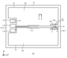
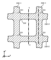
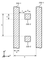
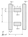
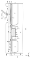
- FIG. 1 is a top view showing an example of the semiconductor device 100.
- the semiconductor device 100 includes a semiconductor substrate 10, an emitter electrode 52, and a gate pad 50.
- the semiconductor substrate 10 is a substrate made of a semiconductor material such as silicon or a compound semiconductor.
- the semiconductor substrate 10 has an end side 102 in a top view. In the present specification, projecting the position of each member onto the upper surface of a predetermined member such as the semiconductor substrate 10 or the semiconductor device 100 is referred to as top view.
- the semiconductor substrate 10 of this example has two sets of end sides 102 facing each other in a top view.
- FIG. 1 shows a set of end sides 102-1 and end sides 102-2 facing each other. In FIG. 1, the direction parallel to the end side 102-1 and the end side 102-2 is the Y-axis direction, and the direction perpendicular to the end side 102-1 and the end side 102-2 is the X-axis direction.
- the emitter electrode 52 and the gate pad 50 are electrodes containing a metal such as aluminum.
- the emitter electrode 52 and the gate pad 50 are separated from each other in a top view.
- a protective member such as polyimide may be provided between the emitter electrode 52 and the gate pad 50.
- An insulating film is provided between the emitter electrode 52 and the gate pad 50 and the semiconductor substrate 10. The emitter electrode 52 and the gate pad 50 are connected to the semiconductor substrate 10 or a member provided on the upper surface of the semiconductor substrate 10 via a contact hole provided in the insulating film.
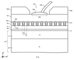
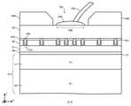
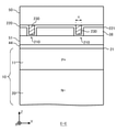
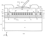
- FIG. 2A is a diagram showing an example of a cross section taken along the line AA in FIG.
- the AA cross section is an XZ plane that passes through the gate pad 50 and the connection portion 204.
- FIG. 2B shows an example of a BB cross section in FIG.
- the BB cross section is an XZ plane passing through the emitter electrode 52.
- the emitter electrode 52 is electrically connected to the semiconductor substrate 10 via the barrier metal layer 220 and the tungsten portion 230 in the contact hole (through hole) 210 provided in the interlayer insulating film 38.
- the emitter electrode 52 may be connected to the source region 22 and the contact region 23 of the first conductive type in the IGBT (insulated gate type bipolar transistor).
- a P-shaped base region 12 is provided below the source region 22, a P-shaped base region 12 is provided below the source region 22, a P-shaped base region 12 is provided below the source region 22, a P-shaped base region 12 is provided.
- the first conductive type is N type.
- a trench 25 may be provided on the surface of the semiconductor substrate 10, and the inside of the trench 25 may be filled with the gate electrode 24 via the insulating film 44.
- the trench 25 of this example is provided on the upper surface 21 of the semiconductor substrate 10 so as to extend in the Y-axis direction. That is, on the upper surface 21 of the semiconductor substrate 10, the trench 25 has a length in the Y-axis direction.
- the gate pad 50 is electrically connected to the wiring layer 51 via the barrier metal layer 220 and the tungsten portion 230 in the contact hole (through hole) 210 provided in the interlayer insulating film 38.
- the wiring layer 51 may be provided on the upper surface of the semiconductor substrate 10 via the insulating film 44.
- the wiring layer 51 is made of polysilicon as an example.
- the gate pad 50 is connected to a gate electrode 24 such as a gate trench in an IGBT. The details of the AA cross section will be described later.
- the emitter electrode 52 may be connected to the source region 22 of the first conductive type in the MOS transistor. In FIG. 1, the insulating film and the contact hole are omitted.
- the emitter electrode 52 may be the electrode having the largest area in the top view among the electrodes provided on the upper surface of the semiconductor substrate 10.
- the gate pad 50 may be arranged between the emitter electrode 52 and the end side 102-1 in a top view.
- the gate pad 50 may be sandwiched between the emitter electrodes 52 in the Y-axis direction.
- Wiring such as a lead frame or wire (not shown) is connected to the upper surface of the emitter electrode 52. Further, a wire wiring portion 202 is connected to the upper surface of the gate pad 50. The wire wiring portion 202 may have a connection portion 204 in contact with the upper surface of the gate pad 50. The connection portion 204 may be a fixing material such as solder, or may be a part of wire wiring. The wire wiring may be ultrasonically bonded or crimped to the upper surface of the emitter electrode 52 at the connection portion 204.
- the semiconductor substrate 10 is provided with an active portion 120.
- the active portion 120 is a region in which a main current flows in the depth direction between the upper surface and the lower surface of the semiconductor substrate 10 when the semiconductor device 100 is controlled to be in the ON state.
- the active portion 120 is a region in which a transistor such as an IGBT or a diode such as an FWD (reflux diode) is provided inside the semiconductor substrate 10.
- the region covered by the emitter electrode 52 may be the active portion 120. In this case, the region sandwiched between the emitter electrodes 52 in the top view may also be the active portion 120.
- the guard ring or the field plate when the guard ring or the field plate is provided in an annular shape along the outer circumference of the semiconductor substrate 10, the region surrounded by the guard ring or the field plate may be used as the active portion 120.
- the guard ring is a P-shaped region provided from the upper surface of the semiconductor substrate 10 to a predetermined depth position.
- the field plate is a conductive member provided above the upper surface of the semiconductor substrate 10. An insulating film is provided between the field plate and the semiconductor substrate 10. The guard ring and the field plate may be provided so as to pass between the gate pad 50 described later and the end side 102-1.
- the emitter electrode 52 is electrically connected to the active portion 120 via a contact hole (through hole 210).
- the gate pad 50 may be connected to a gate runner (wiring layer 51) made of polysilicon, aluminum, or the like via a contact hole.
- the gate voltage applied to the gate pad 50 is supplied to the gate electrode 24 of each transistor portion in the active portion 120 by a gate runner or the like.
- the semiconductor device 100 may include a diode element 178.
- the diode element 178 of this example is a PN junction diode arranged above the semiconductor substrate 10.
- the diode element 178 may function as a temperature detection unit.
- the diode element 178 may be arranged substantially in the center of the semiconductor substrate 10 in the top view.
- the diode element 178 may cover the central position of the semiconductor substrate 10.
- the diode element 178 may be sandwiched between the emitter electrodes 52 in a top view.
- the emitter electrode 52 of this example is divided into at least two regions, and the diode element 178 is sandwiched between the two regions of the emitter electrode 52.
- the semiconductor device 100 may have an anode pad 174 and a cathode pad 176.
- the anode pad 174 is electrically connected to the anode of the diode element 178
- the cathode pad 176 is electrically connected to the cathode of the diode element 178.
- the anode pad 174 and the cathode pad 176 may be connected to the diode element 178 by a wiring made of polysilicon, aluminum or the like.
- the gate pad 50 is arranged on the end side 102-1 side, and the anode pad 174 and the cathode pad 176 are arranged on the end side 102-2 side.
- the end side 102-1 side refers to the end side 102-1 side from the center of the semiconductor substrate 10 in the X-axis direction
- the end side 102-2 side refers to the end side 102-from the center of the semiconductor substrate 10.
- the gate pad 50 may be arranged between the emitter electrode 52 and the end side 102-1.
- the anode pad 174 and the cathode pad 176 may be arranged between the emitter electrode 52 and the end side 102-2.
- a wire wiring portion 202 may be connected to the upper surfaces of the anode pad 174 and the cathode pad 176 in the same manner as the gate pad 50.
- the semiconductor device 100 may further have a current sense pad 172.
- the semiconductor substrate 10 below the current sense pad 172 may be provided with a current sense region 110.
- the current sense region 110 may include a transistor portion that is electrically provided in parallel with the transistor portion in the active portion 120 and has a similar structure. In top view, the current sense region 110 is smaller than the active portion 120. The current flowing through the active portion 120 can be estimated from the current flowing through the current sense region 110.
- the current sense pad 172 may be arranged between the emitter electrode 52 and the end side 102-2. Similar to the gate pad 50, the wire wiring portion 202 may be connected to the upper surface of the current sense pad 172.
- the gate pad 50, the anode pad 174, the cathode pad 176, and the current sense pad 172 shown in FIG. 1 are examples of pad portions.
- the pad portion is not limited to the above-mentioned pad.
- the pad portion is arranged above the upper surface of the semiconductor substrate 10, is made of a metal such as aluminum, and is separated from the emitter electrode 52.
- FIGS. 2A and after the structure in the vicinity of the gate pad 50 will be mainly described, but the vicinity of each pad portion may have the same structure as the vicinity of the gate pad 50.
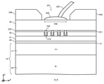
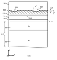
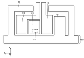
- FIG. 2A is a diagram showing an example of the AA cross section in FIG.
- the AA cross section is an XZ plane that passes through the gate pad 50 and the connection portion 204.
- the semiconductor device 100 of this example has a semiconductor substrate 10, an insulating film 44, a wiring layer 51, an interlayer insulating film 38, a barrier metal layer 220, a tungsten portion 230, a gate pad 50, a connection portion 204, and a wire wiring portion 202 in the cross section.
- a part of the upper surface of the gate pad 50 may be covered with a protective member 240 such as polyimide.
- the region exposed without being covered by the protective member 240 is referred to as the opening region 201.
- connection portion 204 is connected to the upper surface of the gate pad 50 in the opening region 201.
- the portion in contact with the connection portion 204 is referred to as a connection region 206.
- the upper surface of the semiconductor device 100 is sealed with a sealing resin such as silicone gel. As a result, the upper surface of the semiconductor device 100 can be electrically insulated from the outside, and the semiconductor device 100 can be protected from foreign substances such as moisture.
- the semiconductor substrate 10 may have a first conductive type drift region 20 and a second conductive type well region 11.
- the first conductive type is N type and the second conductive type is P type, but the conductive type may be reversed.
- the drift region 20 may also be provided in the entire active portion 120 shown in FIG.
- the well region 11 is provided below the gate pad 50 and between the drift region 20 and the upper surface 21 of the semiconductor substrate 10.
- the wiring layer 51 is provided between the semiconductor substrate 10 and the gate pad 50.
- the wiring layer 51 is made of a conductive material such as polysilicon doped with impurities.
- the wiring layer 51 of this example also functions as the gate runner described above.
- the wiring layer 51 includes a region that overlaps at least a part of the connection region 206 in the top view.
- the wiring layer 51 may include a region that overlaps the entire connection region 206, may include a region that overlaps the entire opening region 201, and may include a region that overlaps the entire gate pad 50.
- An insulating film 44 is provided between the wiring layer 51 and the upper surface 21 of the semiconductor substrate 10.
- the insulating film 44 is, for example, a film obtained by oxidizing or nitriding the upper surface 21 of the semiconductor substrate 10, but is not limited thereto.
- the insulating film 44 may be formed of the same material as the gate insulating film that insulates the gate electrode and the semiconductor substrate 10 in the active portion 120.
- the interlayer insulating film 38 is an insulating layer provided between the wiring layer 51 and the gate pad 50.
- the interlayer insulating film 38 is, for example, boron-doped silicate glass (BPSG: Boron Phosphorus Silicate Glass or BSG: Boron Silicate Glass).
- the interlayer insulating film 38 may be a laminate in which boron-doped silicate glass is laminated on an NSG film.
- the NSG membrane is a membrane composed of NSG (Non-topped Silicate Glass) and not doped with boron and phosphorus.
- the film thickness of the interlayer insulating film 38 is, for example, about 1 ⁇ m, but is not limited thereto.
- the interlayer insulating film 38 is provided with a through hole 210.
- the through hole 210 penetrates from the upper surface 221 of the interlayer insulating film 38 to the lower surface. By filling the through hole 210 with a conductive material, the gate pad 50 and the wiring layer 51 are electrically connected.
- the interlayer insulating film 38 has a through hole 210 at least below the connection region 206.
- the lower part of the connection area 206 is a region that is arranged below the connection area 206 and overlaps with the connection area 206 in the top view.
- the interlayer insulating film 38 of this example may also have a through hole 210 in a region that does not overlap with the connection region 206.
- the tungsten portion 230 is made of a material containing tungsten and is provided inside the through hole 210.
- the tungsten portion 230 may be formed of tungsten, or may be formed of an alloy containing tungsten.
- the upper end of the tungsten portion 230 is in contact with the gate pad 50.
- the lower end of the tungsten portion 230 may be in contact with the wiring layer 51, and may be connected to the wiring layer 51 via another conductive member.
- the tungsten portion 230 may be in contact with the interlayer insulating film 38 or may be in contact with another conductive member inside the through hole 210.
- the barrier metal layer 220 covers the upper surface 221 of the interlayer insulating film 38 at least below the connection region 206.
- the barrier metal layer 220 is made of a material containing titanium.
- the barrier metal layer 220 may be laminated with different materials.
- the barrier metal layer 220 is a laminated body in which a titanium nitride layer is laminated on a titanium layer.
- the titanium layer becomes thin, for example, about several nm or less, and hydrogen can pass through the barrier metal layer 220 and reach the lower layer. Therefore, the semiconductor device is used in the manufacturing process.
- the damage formed inside the 100 can be recovered by annealing in a hydrogen atmosphere.
- the damage is, for example, a dangling bond existing at the interface between the insulating film 44 and the semiconductor substrate 10.
- the titanium layer is as thick as, for example, about 20 nm or more, hydrogen is adsorbed on the titanium layer even if it is annealed in a hydrogen atmosphere, so that hydrogen cannot reach the lower layer of the titanium layer. Therefore, the damage formed inside the semiconductor device 100 cannot be recovered by annealing in a hydrogen atmosphere.
- the thickness of the barrier metal layer 220 including the titanium layer and the titanium nitride layer on the upper surface 221 of the interlayer insulating film 38 may be about 50 nm or more and 200 nm or less.
- the barrier metal layer 220 may also be provided in a region that does not overlap with the connection region 206 in the top view.
- the barrier metal layer 220 may also be provided below the protective member 240. Further, the barrier metal layer 220 may be provided inside the through hole 210 as well.
- the barrier metal layer 220 may cover the side wall of the through hole 210 and the bottom surface. In this case, the barrier metal layer 220 is arranged between the tungsten portion 230 and the wiring layer 51 and the interlayer insulating film 38.
- the electric field inside the semiconductor device 100 causes the resin ions contained in the sealing resin to be separated from the upper surface side of the semiconductor device 100 into the wiring layer 51 or insulation. It reaches the film 44.
- resin ions are trapped in the insulating film 44 and a tunnel current flows more than usual, which adversely affects the characteristics of the semiconductor device 100, such as a decrease in the threshold voltage.
- the barrier metal layer 220 may be provided not only in the active portion 120 but also below the pad portion. It is better to provide the barrier metal layer 220 on the entire lower surface of the pad portion. The entire lower portion of the pad portion is the entire region below the pad portion and overlapping the pad portion when viewed from above. As a result, it is possible to prevent the resin ions from reaching the wiring layer 51 or the insulating film 44 when a part of the electrodes of the pad portion is lost, and to prevent the resin ions from invading the active portion 120 adjacent to the pad portion. It can be suppressed and the threshold voltage does not drop.
- the barrier metal layer 220 containing titanium has relatively low adhesion to the interlayer insulating film 38.
- the adhesion of titanium in the barrier metal layer 220 and a material such as boron in the interlayer insulating film 38 deteriorates.
- the barrier metal layer 220 and the interlayer insulating film 38 are likely to be peeled off when the wire wiring portion 202 is pulled.
- the reason why the barrier metal layer 220 and the interlayer insulating film 38 are easily peeled off is that when the wire wiring portion 202 is pulled, the barrier metal layer 220 and the interlayer insulating film 38 are vertically separated from each other, especially below the connection region 206. This is because stress is applied in the direction.
- the XY interface When the adhesion between the barrier metal layer 220 and the interlayer insulating film 38 at the interface parallel to the XY plane (referred to as the XY interface) is reduced and the structure is not formed at the XY interface, the interlayer between the barrier metal layer 220 and the interlayer is not formed.
- the insulating film 38 is easily peeled off in the vertical direction.
- the case where the structure is not formed at the interface is, for example, the case where the through hole described later is not formed. If the barrier metal layer 220 and the interlayer insulating film 38 are peeled off when the wire wiring portion 202 is pulled, the gate pad 50 on the barrier metal layer 220 will also be removed together with the wire wiring portion 202. ..
- a through hole 210 and a tungsten portion 230 are provided below the connection region 206. Therefore, the area of the XY interface between the interlayer insulating film 38 and the barrier metal layer 220 can be reduced below the connection region 206. Therefore, peeling between the barrier metal layer 220 and the interlayer insulating film 38 can be suppressed.
- the adhesion between the tungsten portion 230 and the barrier metal layer 220 is better than the adhesion between the interlayer insulating film 38 and the barrier metal layer 220.
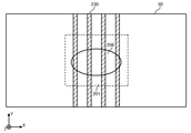
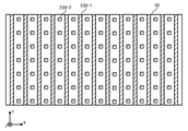
- FIG. 3 is a diagram showing an arrangement example of the tungsten portion 230 in a top view.
- the region overlapping the connection region 206 shown in FIG. 2A is referred to as the connection lower region 208.
- the size and shape of the contiguous zone 208 in top view is the same as the contiguous zone 206.
- the opening region 201 is shown by a broken line.
- the inside of the broken line rectangle is the opening area 201.
- a protective member 240 is provided on the outside of the broken line rectangle, but is omitted in FIG.
- each tungsten portion 230 extends in the Y-axis direction.
- the length of each tungsten portion 230 in the Y-axis direction is larger than the length in the X-axis direction.
- the shape of the tungsten portion 230 in the top view may be striped. By forming the shape of the tungsten portion 230 in the top view into a stripe shape, it is easy to increase the area of the tungsten portion 230 as compared with the case where the tungsten portion 230 has a circular shape in the top view.
- the tungsten portion 230 of this example may be provided from one end to the other end of the gate pad 50 in the Y-axis direction.
- the tungsten portion 230 may be provided in a region inside the end of the gate pad 50. Further, the tungsten portion 230 may extend beyond the end portion of the gate pad 50 in the Y-axis direction. The tungsten portion 230 may be stretched in the X direction. The tungsten portion 230 extending in the X-axis direction and the tungsten portion 230 extending in the Y-axis direction may intersect in a grid pattern.
- the width X1 of each through hole 210 in the X-axis direction may be 0.5 ⁇ m or more and 0.8 ⁇ m or less. Each width X1 may be substantially the same. The width X1 may be measured at the upper end of the through hole 210.
- the width X1 By setting the width X1 to 0.5 ⁇ m or more, when the barrier metal layer 220 is formed on the interlayer insulating film 38, the barrier metal layer 220 having a predetermined thickness can also be formed at the bottom of the through hole 210. Further, by setting the width X1 to 0.8 ⁇ m or less, it is possible to sufficiently leave tungsten inside the through hole 210 when etching back. The outline of the etch back process will be described later.
- the width of the upper end of the through hole 210 may be larger than the width of the lower end of the through hole 210.
- the width of the upper end of the through hole 210 is larger than the width of the lower end of the through hole 210, and the side wall of the through hole 210 is tapered so that the thickness of the barrier metal layer 220 on the side wall of the through hole 210 can be increased.
- the state in which the side wall of the through hole 210 is tapered is a state in which the width of the through hole 210 is continuously narrowed from the upper end to the lower end.
- the width X1 of the upper end of the through hole 210 may be 0.5 ⁇ m
- the width of the lower end of the through hole 210 may be 0.3 ⁇ m.
- a plurality of through holes 210 forming the plurality of tungsten portions 230 are arranged at predetermined intervals along the X-axis direction.
- the distance X2 between the two adjacent through holes 210 may be, for example, 0.5 ⁇ m or more and 3.2 ⁇ m or less.
- the distance X2 may be measured at the upper end of the through hole 210.
- Each distance X2 may be substantially the same.
- the distance X2 may be greater than or equal to the width X1. Since the through hole 210 has the above-mentioned sizes for the width X1 and the distance X2, it is possible to easily form the tungsten portion 230 while suppressing variations in the manufacturing process.
- the distance X2 which is the width at which the interlayer insulating film 38 and the barrier metal layer 220 are in contact with each other at the XY interface, to 3.2 ⁇ m or less, there is an effect of suppressing peeling between the interlayer insulating film 38 and the barrier metal layer 220. ..
- the method for forming the tungsten portion 230 may be as follows. First, a through hole 210 is formed in the interlayer insulating film 38 by photolithography and dry etching. Next, the barrier metal layer 220 is formed inside the through hole 210 and on the interlayer insulating film 38. Next, tungsten is formed inside the through hole 210 and on the interlayer insulating film 38, and the inside of the through hole 210 is filled with tungsten. Next, the tungsten portion 230 is formed by etching back. Here, the etch back is a process of removing the tungsten film on the interlayer insulating film 38 by etching, leaving the tungsten inside the through hole 210. The above is an example of a method for forming the tungsten portion 230. The tungsten portion 230 of the gate pad 50 may be formed at the same time as the tungsten portion 230 of the active region shown in FIG. 16 described later.
- the width of the connection lower region 208 in the X-axis direction is defined as X3.
- the width X6 of each tungsten portion 230 in the X-axis direction is smaller than the width X3.
- the width X6 may be half or less of the width X3 and may be 1/3 or less.
- the distance X7 in the X-axis direction of the adjacent tungsten portions 230 is smaller than the width X3.
- the distance X7 may be less than or equal to half of the width X3 and may be less than or equal to 1/3.
- the connection lower region 208 may include a plurality of tungsten portions 230 arranged in the X-axis direction.
- connection lower region 208 the area of the region where the through hole 210 is formed in the top view is S1, and the total area of the connection lower region 208 is S.
- the area S1 of the through hole 210 is preferably 20% or more of the area S of the connection lower region 208. That is, in the connection lower region 208, the area of the XY interface between the barrier metal layer 220 and the gate pad 50 is affected by the thickness of the barrier metal layer 220 on the side wall of the through hole 210, but the area S of the connection lower region 208. It may be about 0% or more and about 80% or less.
- the through hole 210 By providing the through hole 210, the area of the XY interface between the interlayer insulating film 38 having weak adhesion and the barrier metal layer 220 is reduced so that the interlayer insulating film 38 and the barrier metal layer 220 do not peel off, and by peeling. It is possible to prevent the occurrence of defects in which the gate pad 50 is removed.
- FIG. 4 is a diagram showing an example of the results of a tensile test on a plurality of semiconductor devices 100.
- the wire wiring portion 202 is pulled upward to test whether or not the gate pad 50 is peeled from the interlayer insulating film 38.
- the wire wiring portion 202 or the connection portion 204 is broken before the gate pad 50 is peeled off, it is determined to be a non-defective product.
- the rate at which the gate pad 50 is removed before the wire wiring portion 202 or the connection portion 204 is broken is defined as the peeling occurrence rate.
- the vertical axis shows the peeling occurrence rate
- the horizontal axis shows the area ratio S1 / S between the area where the through hole 210 is formed in the connection lower region 208 and the connection lower region 208 in 100%.
- the wire used in the tensile test was 400 ⁇ m in diameter or 500 ⁇ m in diameter. In the tensile test, tests using wires of other diameters were also conducted, but no significant wire diameter dependence was observed.
- the wire may be made of aluminum or may be made of a compound containing aluminum as a main component. For example, silicon may be added to the wire.
- the area ratio S1 / S is preferably 20% or more.
- the area ratio may be 50% or more, and may be 100%.
- the area of the opening region 201 in the top view is S 201 .
- the area of the tungsten portion 230 viewed from above is defined as S1'.
- the area ratio S1'/ S 201 may be 20% or more, 50% or more, or 100%.
- the position of the connection lower region 208 may vary. Therefore, if the area ratio S1'/ S 201 is set to 20% or more, the gate pad 50 can be removed. It is effective in suppressing the occurrence of defects. That is, even if the position of the wire bond connection lower region 208 varies, it is effective to always set the area ratio S1 / S to 20% or more in order to suppress the defect that the gate pad 50 is removed.
- the area of the gate pad 50 in the top view is S50. Further, in the region below the gate pad 50, the area of the tungsten portion 230 viewed from above is S1''.
- the area ratio S1'' / S50 may be 0.3% or more, 20% or more, 50 % or more, or 100%. That is, it is important that the area ratio S1 / S is 20% or more in order to suppress the occurrence of defects in which the gate pad 50 is removed, and other than the connection lower region 208, for example, the opening region 201.
- the area of the tungsten portion may be small. Since it is effective to set the area ratio S1 / S to 20% or more to suppress the defect that the gate pad 50 is removed, in FIG. 2A, the width X1 and the distance X2 of the through hole 210 are the area ratio S1.
- the relational expression of X1 / (X1 + X2) ⁇ 0.2 may be satisfied so that / S is 20% or more.
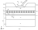
- FIG. 5 is a diagram showing another example of the AA cross section.
- This example is a cross-sectional structure when the width X1 of the through hole 210 in the X-axis direction is larger than 0.8 ⁇ m.
- the through hole 210 may have a striped shape extending in the Y-axis direction, as in the above example.
- the area ratio S1 / S is larger than 50%. It's okay.
- the semiconductor device 100 of this example has a structure of the tungsten portion 230, the through hole 210, the barrier metal layer 220, and the interlayer insulating film 38 different from the example of FIG. 2A. Other structures are similar to the example in FIG. 2A.
- FIG. 6 is a diagram showing an example of arrangement of the tungsten portion 230 in the semiconductor device 100 shown in FIG. 5 in a top view.
- the tungsten portion 230 is provided as a whole in the top view of the connection lower region 208.
- the width of the tungsten portion 230 in the X-axis direction is larger than the width X3 of the connection lower region 208.
- the end of the tungsten portion 230 of this example is arranged below the gate pad 50 and above the barrier metal layer 220 in a region other than the connection lower region 208.
- the lower part of the gate pad 50 is a region which is arranged below the gate pad 50 and overlaps with the gate pad 50 in the upper view.
- a barrier metal layer 220 is provided between the tungsten portion 230 and the upper surface 221 of the interlayer insulating film 38.
- the tungsten portion 230 may cover the entire region below the opening region 201 in the top view, or may cover the entire region below the gate pad 50.
- the interlayer insulating film 38 in the connection lower region 208 is provided with the through hole 210, the XY interface between the upper surface 221 of the interlayer insulating film 38 and the barrier metal layer 220 is not provided with the through hole 210. Less than in the case. As a result, it is possible to suppress the peeling of the interlayer insulating film 38 and the barrier metal layer 220 and prevent the gate pad 50 from being removed.
- the width X1 of the through hole 210 in this example is larger than 0.8 ⁇ m, sufficient tungsten cannot be left in the through hole 210 when etching back the tungsten in the above-mentioned method for forming the tungsten portion 230. .. This is because when the tungsten is etched back, the tungsten inside the through hole 210 is also etched. Further, when etching back, the tungsten that could not be removed remains inside the through hole 210, which may cause a problem in the subsequent process. Problems in the subsequent steps include, for example, that the tungsten remaining in the through hole 210 due to etch back is peeled off from the barrier metal layer 220 and becomes a foreign substance.
- the width X1 when the width X1 is larger than 0.8 ⁇ m, it is preferable not to etch back the tungsten.
- the structures shown in FIGS. 5 and 6 can be formed by not etching back the tungsten after deposition. Further, in the region where the gate runner surrounding the active portion 120 is formed, the tungsten on the interlayer insulating film 38 may be etched together with the gate pad 50 and the barrier metal layer 220. This prevents the gate pad 50 and the emitter electrode 52 from being electrically connected.
- the width X1 may be larger than the distance X2 between the two adjacent through holes 210.
- the width X1 may be at least twice the distance X2 and may be at least three times.
- the width X1 may be larger than the width of the interlayer insulating film 38 in the X-axis direction. Further, the width X1 may be smaller or larger than the width X3 of the connection lower region 208.
- a plurality of through holes 210 arranged in the X-axis direction are provided below the connection portion 204. In another example, below the connection portion 204, only one through hole 210 may be included among the plurality of through holes 210 arranged in the X-axis direction.
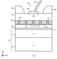
- FIG. 7 is a diagram showing another example of the AA cross section.
- the area ratio S1 / S is 100% when the area of the region where the through hole 210 is formed is S1 and the total area of the connection lower region 208 is S. Is.
- the semiconductor device 100 of this example has a structure of the tungsten portion 230, the through hole 210, the barrier metal layer 220, and the interlayer insulating film 38 different from the example of FIG. 2A. Other structures are similar to the example in FIG. 2A.
- FIG. 8 is a diagram showing an example of arrangement of the tungsten portion 230 in the semiconductor device 100 shown in FIG. 7 in a top view.
- the tungsten portion 230 and the through hole 210 are provided in the entire upper view of the connection lower region 208.
- the width of the tungsten portion 230 in the X-axis direction is larger than the width X3 of the connection lower region 208.
- the interlayer insulating film 38 is not provided in the connection lower region 208 of this example.
- the XY interface between the upper surface 221 of the interlayer insulating film 38 and the barrier metal layer 220 does not exist in the connection lower region 208, and the XY interface between the upper surface 221 of the interlayer insulating film 38 and the barrier metal layer 220 is peeled off. It is possible to prevent the gate pad 50 from coming off.
- the tungsten portion 230 may cover a part of the upper surface 221 of the interlayer insulating film 38.
- a barrier metal layer 220 may be provided between the tungsten portion 230 and the upper surface 221 of the interlayer insulating film 38.
- the tungsten portion 230 of this example is arranged below the gate pad 50 and above the interlayer insulating film 38 in a region other than the connection lower region 208.
- the tungsten portion 230 may cover the entire region below the opening region 201 in the top view, or may cover the entire region below the gate pad 50.
- the through hole 210 is provided in a part of the area below the gate pad 50 including the connection lower area 208.
- the through hole 210 may be provided in a region smaller than the opening region 201 in the top view, may be provided in the same region as the opening region 201, or may be provided in a region larger than the opening region 201.
- Below the gate pad 50 one through hole 210 including the connection lower region 208 may be provided, and a through hole 210 may be provided in addition to the connection lower region 208.
- the tungsten portion 230 provided inside the through hole 210 and the tungsten portion 230 provided above the interlayer insulating film 38 may be continuous.
- a through hole 210 is formed in the interlayer insulating film 38, and after laminating the barrier metal layer 220, tungsten is deposited inside the through hole 210 and above the interlayer insulating film 38.
- the structure shown in FIGS. 7 and 8 can be formed by not etching back the tungsten after deposition.
- the tungsten on the interlayer insulating film 38 may be etched together with the gate pad 50 and the barrier metal layer 220. This prevents the gate pad 50 and the emitter electrode 52 from being electrically connected.
- FIG. 9 is a diagram showing another example of the AA cross section.
- the tungsten portion 230 and the through hole 210 are provided only below the connection region 206 or the opening region 201, and are provided in other regions below the gate pad 50. It differs from the examples in FIGS. 1 to 8 in that it does not.
- the area of the gate pad 50 in the top view is S50.
- the area of the tungsten portion 230 viewed from above is S1''.
- the area ratio S1'' / S50 may be 0.3% or more.
- Other structures are similar to any of the examples in FIGS. 1-8.
- the XY interface between the barrier metal layer 220 and the interlayer insulating film 38 in the connection lower region 208 where peeling is likely to occur can be reduced, and the XY interface between the upper surface 221 of the interlayer insulating film 38 and the barrier metal layer 220 is peeled off. By doing so, it is possible to prevent the gate pad 50 from being removed.
- FIG. 10 is a diagram showing an example of arrangement of the tungsten portion 230 in the semiconductor device 100 shown in FIG. 9 in a top view.
- each tungsten portion 230 is arranged so as to overlap the connection lower region 208 or the opening region 201.
- each tungsten portion 230 may extend to the outside of the connection lower region 208 or the opening region 201 in the Y-axis direction.
- the tungsten portion 230 may be extended to a position where it overlaps with the end portion of the gate pad 50 in the Y-axis direction.
- each tungsten portion 230 may be provided only in the region overlapping the connection lower region 208 or the opening region 201 even in the Y-axis direction.
- FIG. 11 is a diagram showing another example of the AA cross section.
- the density of the tungsten portion 230 and the through hole 210 is different between the region below the connection region 206 or the opening region 201 and the other region.
- Other structures are similar to any of the examples of FIGS. 1-10.
- the density of the tungsten portion 230 and the through hole 210 in the region below the connection region 206 or the opening region 201 is higher than the density in the other regions. That is, in the region below the connection region 206 or the opening region 201, the tungsten portion 230 and the through hole 210 having a higher area ratio are provided.
- the widths of the through holes 210 and the tungsten portion 230 in the X-axis direction are the same.
- the period in which the tungsten portion 230 and the through hole 210 are arranged in the X-axis direction is shorter than the period in the other regions.
- the XY interface between the barrier metal layer 220 and the interlayer insulating film 38 in the connection lower region 208 where peeling is likely to occur can be reduced, and the XY interface between the upper surface 221 of the interlayer insulating film 38 and the barrier metal layer 220 is peeled off. By doing so, it is possible to prevent the gate pad 50 from being removed.
- FIG. 12 is a diagram showing an example of arrangement of the tungsten portion 230 in the semiconductor device 100 shown in FIG. 11 in a top view. As described above, the period in the X-axis direction of the tungsten portion 230 overlapping the connection region 206 or the opening region 201 is shorter than the period in the other regions.
- FIG. 13 is an enlarged cross-sectional view of the vicinity of the through hole 210.
- the width of the lower end may be narrower than the width of the upper end of the through hole 210.
- the upper end of the tungsten portion filled in the through hole 210 may have a dent formed by etch back.
- the thickness of the barrier metal layer 220 provided on the upper surface 221 of the interlayer insulating film 38 is Z1
- the thickness of the barrier metal layer 220 provided on the side surface of the through hole 210 is Z2
- the thickness of the barrier metal layer 220 provided on the lower end of the through hole 210 is Z1. Assuming that the thickness of 220 is Z3, the relationship of Z1> Z2> Z3 is established.
- the thicknesses Z1 and Z3 are lengths in the Z-axis direction.
- Z2 is the length in the direction perpendicular to the side wall of the through hole 210.
- the barrier metal layer 220 on the side surface of the through hole 210 and the barrier metal layer 220 on the bottom surface prevent resin ions from reaching below the barrier metal layer 220 when the gate pad 50 is defective even if the thickness is thin. be able to. This is because there is a tungsten portion 230 in the through hole 210.
- a part of titanium deposited on the bottom surface of the through hole 210 is bonded to silicon contained in the wiring layer 51, so that an alloy of titanium and silicon is formed under the barrier metal layer 220 on the bottom surface of the through hole 210. May be done.
- FIG. 14 is a diagram showing an arrangement example of the connection region 206 on the upper surface of the gate pad 50.
- the connection area 206 is an area where the connection portion 204 is provided.
- a plurality of strip-shaped tungsten portions 230 and through holes 210 extending in the first direction (Y-axis direction in this example) are provided.
- the long axis of the connection region 206 is indicated by a chain line 209.
- the long axis of the connection area 206 is the axis on which the length of the connection area 206 becomes maximum in the XY plane.
- the direction in which the chain wire 209 extends is defined as the second direction.
- the angle ⁇ between the first direction and the second direction may be 10 degrees or less.
- the angle ⁇ may be 5 degrees or less, or may be 0 degrees. That is, the long axis of the connection region 206 and the stretching direction of the tungsten portion 230 may be substantially parallel.
- FIG. 15 is a diagram showing another arrangement example of the connection region 206 on the upper surface of the gate pad 50.
- the angle ⁇ with the first direction and the second direction is 30 degrees or more.
- the angle ⁇ may be 45 degrees or more, and may be 60 degrees or more.
- the number of tungsten portions 230 straddled by the connection portion 204 can be increased.
- the connecting portion 204 is a fixing member such as solder, the connection between the connecting portion 204 and the gate pad 50 can be strengthened.
- FIG. 16 is a diagram showing an example of an XZ cross section in the active portion 120.
- An N-type region such as an emitter region, a P-type region such as a collector region, a gate electrode, a gate insulating film, and the like are formed on the semiconductor substrate 10, but they are omitted in FIG.
- an interlayer insulating film 38, a through hole 210, a barrier metal layer 220, and a tungsten portion 230 may be provided between the emitter electrode 52 and the upper surface 21 of the semiconductor substrate 10.
- the barrier metal layer 220 and the tungsten portion 230 may electrically connect the emitter electrode 52 and the upper surface 21 of the semiconductor substrate 10.
- the width of the tungsten portion 230 or the through hole 210 in the active portion 120 in the X-axis direction is X4.
- the width X4 of the tungsten portion 230 or the through hole 210 in the active portion 120 may be different from the width X1 of the tungsten portion 230 or the through hole 210 in the connection lower region 208 described with reference to FIGS. 1 to 15.
- the distance X5 of the through hole 210 in the active portion 120 in the X-axis direction may be different from the distance X2 of the through hole 210 in the connection lower region 208.
- the width X1 of the through hole 210 in the connection lower region 208 may be smaller than the width X4 of the through hole 210 below the emitter electrode 52.
- the width X1 may be smaller than the width X4 is that the gate pad 50 does not have an element structure such as a gate electrode and a gate insulating film, so that it has better flatness than the active portion 120 and is easy to microfabricate. Is.
- the tungsten portion 230 and the through hole 210 in the active portion 120 have a width X4 and a distance X5 suitable for drawing out the carrier, and the tungsten portion 230 and the through hole 210 in the connection lower region 208 have a gate pad 50 and a wiring layer. It has a connection of 51 and a width X1 and a distance X2 suitable for suppressing peeling of the gate pad 50.
- the interlayer insulating film 38, the through hole 210, the barrier metal layer 220, and the tungsten portion 230 may be formed in the same manufacturing process in the region below the active portion 120 and the gate pad 50.
- the ratio S1 / S of the area S1 of the tungsten portion 230 provided in the active portion 120 to the total area S of the active portion 120 is 20% or more as in the gate pad 50. Further, the S1 / S of the active portion 120 may be about 25%.
- FIG. 17 is a diagram showing another arrangement example of the tungsten portion 230 and the through hole 210 in the top view.
- the tungsten portion 230 and the through hole 210 of this example are provided in a spiral shape in a region overlapping with the gate pad 50.
- the center (or end point) of the swirl may be located in the connection lower region 208.
- the through hole 210 is formed in substantially the same region as the tungsten portion 230.
- the area of the region where the through hole 210 is formed in the top view is S1
- the entire area of the connection lower region 208 is S
- the area ratio S1 / S is 20% or more. ..
- the through hole 210 is omitted.
- the tungsten portion 230 and the through hole 210 may not be arranged on the outside of the opening region 201.
- FIG. 18 is a diagram showing another arrangement example of the tungsten portion 230 and the through hole 210 in the top view.
- the tungsten portion 230 and the through hole 210 are arranged discretely in the X-axis direction and continuously arranged in the Y-axis direction.
- the tungsten portion 230 and the through hole 210 of this example are arranged discretely in the Y-axis direction.
- Other structures are similar to any of the examples of FIGS. 1-16.
- the tungsten portion 230 and the through hole 210 may be arranged discretely in two directions, for example, in the X-axis direction and the Y-axis direction. Although the description of the through hole 210 is omitted in FIG.
- the through hole 210 is formed in substantially the same region as the tungsten portion 230.
- the area of the region where the through hole 210 is formed in the top view is S1
- the area ratio S1 / S where the entire area of the connection lower region 208 is S is 20% or more. do.
- FIG. 19 is a diagram showing an example of a CC cross section of FIG.
- the CC cross section is an XZ plane that passes through the gate pad 50 and the connection portion 204.
- FIG. 19 has the same structure as that of FIG. 2A.
- the length of the through hole 210 in the X-axis direction is defined as the width X1.
- a plurality of tungsten portions 230 are arranged at predetermined intervals along the X-axis direction. Let X2 be the distance between two adjacent through holes 210 in the X-axis direction.
- FIG. 20 is a diagram showing an example of a DD cross section of FIG.
- the DD cross section is a YZ plane that passes through the gate pad 50 and the connection portion 204.
- the length of the through hole 210 in the Y-axis direction is defined as the width Y1.
- a plurality of tungsten portions 230 are arranged at predetermined intervals along the Y-axis direction. Let Y2 be the distance between two adjacent through holes 210 in the Y-axis direction.
- the area ratio S1 / S in which the area of the region where the through hole 210 is formed in the top view is S1 and the entire area of the connection lower region 208 is S is 20% or more.
- X1 may be 0.5 ⁇ m
- X2 may be 1.5 ⁇ m
- Y1 may be 5.0 ⁇ m
- Y2 may be 1.0 ⁇ m
- the through hole 210 is omitted.
- the tungsten portion 230 and the through hole 210 may not be arranged on the outside of the opening region 201.
- the interlayer insulating film 38 may be a BPSG film or a BSG film.
- the boron concentration in the interlayer insulating film 38 may be 2.6 wt% or more and 5 wt% or less. More preferably, it may be 2.7 wt% or more and 4.0 wt% or less. In addition, wt% indicates the weight percent concentration. If the boron concentration is too low, it becomes difficult to manufacture the interlayer insulating film 38.
- the reason why the interlayer insulating film 38 is difficult to manufacture is that, for example, when the interlayer insulating film 38 is heat-treated, deformation due to fluidization is unlikely to occur, a dent remains in the interlayer insulating film 38 above the trench gate, and the tungsten film is etched back. This is because tungsten tends to remain in the dent. Further, if the boron concentration is too high, the reaction between titanium in the barrier metal layer 220 and boron tends to occur, the adhesion between the barrier metal layer 220 and the interlayer insulating film 38 becomes low, and peeling easily occurs at this interface. Become.
- FIG. 21 is a diagram showing another arrangement example of the tungsten portion 230 and the through hole 210 in the top view.
- the opening region 201 and the connection lower region 208 are omitted, but the opening region 201 and the connection lower region 208 are provided at the same positions as those in FIGS. 1 to 20.
- the through hole 210 and the tungsten portion 230 is provided along the first stretching direction (for example, the Y-axis direction) parallel to the upper surface 21 of the semiconductor substrate 10.
- the through hole 210 and a part of the tungsten portion 230 are provided in parallel with the upper surface 21 of the semiconductor substrate 10 and along the second stretching direction (for example, the X-axis direction) different from the first stretching direction.
- the tungsten portion 230 is shown in FIG. 21, the through hole 210 is also arranged at a position corresponding to the tungsten portion 230.
- the semiconductor device 100 of this example has a tungsten portion 230-1 and a tungsten portion 230-2 extending in different directions on the XY plane.
- the tungsten portion 230-1 of this example is provided so as to extend in the Y-axis direction.
- the tungsten portion 230-1 is a strip-shaped portion having a length in the Y-axis direction.
- the tungsten portion 230-2 of this example is provided so as to extend in the X-axis direction.
- the tungsten portion 230-2 is a strip-shaped portion having a length in the X-axis direction.
- the tungsten portion 230-1 and the tungsten portion 230-2 may be connected.
- the through hole 210 has a through hole connecting portion 231 at a position where the tungsten portion 230-1 and the tungsten portion 230-2 are connected.
- the through-hole connection portion 231 of this example is a portion where the through-hole 210 provided along the Y-axis direction and the through-hole 210 provided along the X-axis direction merge.
- the tungsten portion 230-1 and the tungsten portion 230-2 may intersect in the XY plane. That is, the tungsten portion 230-1 and the tungsten portion 230-2 may be provided so as to penetrate each other on the XY plane.
- the tungsten portions 230-1 may be arranged at a predetermined cycle in the X-axis direction.
- the tungsten portions 230-2 may be arranged at a predetermined cycle in the Y-axis direction.
- the tungsten portion 230-1 and the tungsten portion 230-2 may be arranged in a grid pattern on the XY plane. In this case, the through hole connecting portion 231 is arranged at a predetermined cycle in each of the X-axis direction and the Y-axis direction.
- FIG. 22 is an enlarged view of the tungsten portion 230-1 and the tungsten portion 230-2 shown in FIG. 21.
- the spacing between the through-hole connecting portions 231 arranged along the X-axis direction is a
- the spacing between the through-hole connecting portions 231 arranged along the Y-axis direction is b
- the spacing is arranged along the X-axis direction.
- c be the width of the through hole 210
- d the width of the through hole 210 arranged along the Y-axis direction.
- the width of the through hole 210 the width of the tungsten portion 230 may be used.
- the interval between the through hole connecting portions 231 may use the cycle in which the tungsten portion 230 is arranged.
- the distance between the two through-hole connection portions 231 is the distance between the corresponding positions in the respective through-hole connection portions 231.
- the distance between the centers of the through-hole connection portions 231 may be the distance between the through-hole connection portions 231.
- the distance between the ends of the through hole connecting portion 231 on the same side may be set as the distance between the through hole connecting portions 231.
- the intervals a and b and the widths c and d may satisfy the following equation. ((A ⁇ c) + (bc) ⁇ d) / (a ⁇ b) ⁇ 0.2 That is, in the unit area a ⁇ b, the area (a ⁇ c) + (bc) ⁇ d) occupied by the through hole 210 or the tungsten portion 230 may be 20% or more. The area ratio may be 25% or more, and may be 30% or more. The same applies to the examples described with reference to FIGS. 1 to 20.
- FIG. 23 is a diagram showing another shape example of the through hole 210 and the tungsten portion 230.
- the through hole 210 and the tungsten portion 230 of this example may have a curved portion 232 in an XY plane parallel to the upper end of the through hole 210.
- the width of the through hole connecting portion 231 may be larger than the width of the through hole 210 in other portions. For example, as shown in FIG.
- etching may proceed in the XY plane, and a curved portion 232 may appear on the upper surface shapes of the through hole 210 and the tungsten portion 230.
- the width of the through hole 210 and the tungsten portion 230 in the through hole connecting portion 231 becomes larger than the width of the through hole 210 and the tungsten portion 230 in the other portions.
- FIG. 24 is a diagram showing an example of an EE cross section in FIG. 23.
- the EE cross section is a YZ plane that intersects the tungsten portion 230-2 at a position different from that of the tungsten portion 230-1.
- the connection portion 204 or the like provided on the gate pad 50 is omitted, but as in the example of FIG. 20, the connection portion 204, the wire wiring portion 202, and the wire wiring portion 202 are above the gate pad 50.
- the protective member 240 is provided.
- the connection portion 204, the wire wiring portion 202, and the protective member 240 may be omitted.
- the area of the XY interface between the interlayer insulating film 38 and the barrier metal layer 220 can be reduced. Therefore, peeling between the barrier metal layer 220 and the interlayer insulating film 38 can be suppressed.
- FIG. 25 is a diagram showing an example of an FF cross section in FIG. 23.
- the FF cross section is a YZ plane that passes through the through hole connecting portion 231 along the tungsten portion 230-1.
- the upper end of the tungsten portion 230 provided in the through hole connecting portion 231 is arranged below the upper end of the tungsten portion 230 provided in the through hole 210 other than the through hole connecting portion 231. That is, the upper surface of the tungsten portion 230 is recessed in the through hole connecting portion 231 toward the upper surface 21 of the semiconductor substrate 10.
- the width of the through hole 210 is large in the vicinity of the through hole connecting portion 231.
- the through hole 210 is filled with tungsten, a dent is likely to occur in the through hole connecting portion 231.
- the contact area between the gate pad 50 and the tungsten portion 230 is increased, so that the adhesion between the gate pad 50 and the tungsten portion 230 can be improved.
- z2 be the thickness of the tungsten portion 230 in the region other than the through hole connecting portion 231.
- the maximum value of the thickness of the tungsten portion 230 may be used.
- z1 be the depth of the recess of the tungsten portion 230 in the through hole connecting portion 231.
- the depth z1 may be 5% or more of the thickness z2, 10% or more, or 20% or more.
- the depth z1 may be 50% or less of the thickness z2, and may be 30% or less.
- the adhesion between the tungsten portion 230 and the gate pad 50 can be improved while maintaining the thickness of the tungsten portion 230 to a certain extent.
- c' be the width of the depression on the upper surface of the tungsten portion 230.
- the width c'in this example is the width in the Y-axis direction.
- the width c' may be larger than the width c of the tungsten portion 230-2.
- FIG. 26 is a diagram showing another arrangement example of the tungsten portion 230 and the through hole 210 in the top view.
- the tungsten portion 230-1 is connected to the tungsten portion 230-2, but does not penetrate the tungsten portion 230-2. That is, the tungsten portion 230-1 is connected to the tungsten portion 230-2 in a T shape.
- Other structures are similar to the example in FIG.
- a through hole connecting portion 231 is provided at the connecting portion between the tungsten portion 230-1 and the tungsten portion 230-2.
- FIG. 27 is an enlarged view of the tungsten portion 230-1 and the tungsten portion 230-2 shown in FIG. 26.
- the tungsten portion 230-1 is connected to the tungsten portion 230-2 in a T-shape.
- Other structures are similar to those in FIG. 22 or 23.
- the spacing between the through-hole connecting portions 231 arranged along the X-axis direction is a
- the spacing between the through-hole connecting portions 231 arranged along the Y-axis direction is b
- the spacing is arranged along the X-axis direction.
- the intervals a and b and the widths c and d may satisfy the following equation. ((A ⁇ c) + (bc) ⁇ d) / (a ⁇ b) ⁇ 0.2 That is, in the unit area a ⁇ b, the area (a ⁇ c) + (bc) ⁇ d) occupied by the through hole 210 or the tungsten portion 230 may be 20% or more. The area ratio may be 25% or more, and may be 30% or more.
- FIG. 28 is a diagram showing another arrangement example of the tungsten portion 230 and the through hole 210 in the top view.
- at least one of the tungsten portion 230-1 and the tungsten portion 230-2 is discretely arranged in the stretching direction.
- the tungsten portions 230-2 are arranged discretely along the X-axis direction.
- the tungsten portions 230-2 are also arranged discretely in the Y-axis direction.
- the trench 25 is provided so as to extend in the Y-axis direction.
- the tungsten portion 230-1 extending in the Y-axis direction and the through hole 210 are continuously provided in the gate pad 50 in the Y-axis direction.
- the tungsten portions 230-2 are discretely arranged. With such a configuration, the unevenness of the upper surface of the tungsten portion 230 can be reduced in the direction parallel to the trench 25, and the variation in the connectivity between the trench 25 and the gate pad 50 can be reduced.
- the tungsten portions 230-2 may be provided continuously in the X-axis direction, and the tungsten portions 230-1 may be provided discretely in the Y-axis direction.
- the tungsten portion 230-2 may be arranged at a predetermined cycle in the X-axis direction.
- the tungsten portion 230-2 may be connected to or separated from the tungsten portion 230-1.
- a through hole connecting portion 231 may be provided at the connecting portion.
- one tungsten portion 230-2 may be arranged between the two tungsten portions 230-1 in the X-axis direction.
- two or more tungsten portions 230-2 may be arranged between the two tungsten portions 230-1 in the X-axis direction.
- FIG. 29 is an enlarged view of the tungsten portion 230-1 and the tungsten portion 230-2 shown in FIG. 28.
- the tungsten portion 230-1 and the tungsten portion 230-2 are separated from each other.
- Other structures are similar to those in FIG. 22 or 23.
- the space between the through-hole connection portions 231 arranged along the X-axis direction is filled with a
- the space between the through-hole connection parts 231 arranged along the Y-axis direction is filled with b
- the tungsten portion 230-2 is filled.
- c be the width of the through hole 210 formed in the Y-axis direction
- d be the width of the through hole 210 arranged along the Y-axis direction.
- the width of the through hole 210 filled with the tungsten portion 230-2 in the X-axis direction is set to e
- f be the distance in the X-axis direction. The distance f is the shortest distance between the tungsten portion 230-1 and the tungsten portion 230-2.
- the intervals a, b, widths c, d, e, and distance f may satisfy the following equation. ((B ⁇ d) + (e ⁇ c)) / (a ⁇ b) ⁇ 0.2 That is, in the unit area a ⁇ b, the area (b ⁇ d) + (e ⁇ c) occupied by the through hole 210 or the tungsten portion 230 may be 20% or more.
- the area ratio may be 25% or more, and may be 30% or more.
- FIG. 30 is an enlarged view showing another example of the tungsten portion 230-1 and the tungsten portion 230-2 shown in FIG. 28.
- each tungsten portion 230-2 has a length in the X-axis direction. That is, the width e is larger than the width c.
- the width e may be the same as the width c, and the width e may be smaller than the width c.
- the tungsten portion 230-1 provided along the Y-axis direction and the tungsten portion 230-2 provided along the X-axis direction may be arranged apart from each other.
- the width e may be larger than the distance f.
- FIG. 31 is a diagram showing an arrangement example of the gate runner 60 in the semiconductor device 100.
- the gate runner 60 is shown by a broken line.
- the gate runner 60 is a wiring for connecting the gate pad 50 and the gate electrode 24 shown in FIG. 2B.
- a gate potential is applied to the gate runner 60 from the gate pad 50.
- the gate runner 60 of this example is provided above the semiconductor substrate 10.
- the gate runner 60 is made of a conductive material such as polysilicon to which impurities have been added.
- each pad is different from the example of FIG. 1, but the arrangement of the pads may be the same as the example of FIG.
- the anode pad 174, the current sense pad 172, the cathode pad 176 and the gate pad 50 are arranged in order along the end side 102-2.
- the gate runner 60 is arranged so as to surround the active portion 120. Further, the gate runner 60 may also be arranged between each pad and the active portion 120.
- FIG. 32 is an enlarged top view of the vicinity of each pad.
- the anode pad 174, the current sense pad 172, the cathode pad 176 and the gate pad 50 are arranged in order along the Y-axis direction.
- Each pad may be provided with the wire wiring portion 202 and the connection portion 204 described in FIG. 2A and the like.
- a part of the gate metal portion 80 is arranged so as to surround the anode pad 174, the current sense pad 172, the cathode pad 176, and the gate pad 50.
- the anode pad 174, the current sense pad 172, the cathode pad 176, the gate pad 50 and the gate metal portion 80 may be formed in the same process.
- the gate pad 50 and the gate metal portion 80 may be connected to each other.
- FIG. 33 is a top view showing an example of arrangement of the gate runner 60 in the vicinity of each pad.
- the gate runner 60, the separated conductive portion 71 below the current sense pad 172, the separated conductive portion 70 below the anode pad 174, and the separated conductive portion 72 below the cathode pad 176 are hatched with diagonal lines. is doing.
- the gate runner 60 is provided in the height direction (Z direction) in the region between the upper surface 21 of the semiconductor substrate 10 and each pad.
- the arrangement of each pad is the same as in FIG. 32.
- the gate runner 60, the separated conductive portion 70, the separated conductive portion 71, and the separated conductive portion 72 may be formed in the same process.
- a part of the gate runner 60 is arranged below the gate pad 50.
- the gate runner 60 is electrically connected to the gate pad 50 via a contact hole or the like.
- the gate runner 60 may be provided along the edge 102 (see FIG. 31) of the semiconductor substrate 10 so as to surround the active portion 120 (see FIG. 31).
- the gate runner 60 is electrically connected to the gate electrode 24 of the transistor portion of the current sense region 110.
- the current sense region 110 has a structure similar to that of the transistor portion shown in FIG. 2A. A portion of the gate runner 60 may be located below the current sense pad 172.
- the current sense region 110 has a small area of 1/1000 or less of the active portion 120.
- the current sense region 110 is connected to an IC that detects the flowing current.
- the IC detects the voltage generated when the generated current flows between the sense resistors, and cuts off the current flowing through the semiconductor device 100 when it is determined that the current is flowing too much.
- the diode element 178 (see FIG. 31) that detects the temperature has a PN diode formed in series at the center of the chip and has a temperature dependence.
- the diode element 178 is an example of a sense unit that detects a temperature rise by the connected IC. Current and temperature are examples of physical information.
- the anode pad 174, the current sense pad 172, and the cathode pad 176 are examples of the sense pad portion connected to the sense portion.
- the sense unit and the sense pad unit are not limited to these examples.
- Separation conductive portions 70, 71, 72 separated from the gate runner 60 are provided between the anode pad 174, the current sense pad 172 and the cathode pad 176, and the upper surface 21 of the semiconductor substrate 10.
- the separated conductive portions 70, 71, 72 are formed of a conductive material, and are insulated from the gate runner 60 by an insulating film or the like.
- the separated conductive portions 70, 71, 72 may be formed of the same material as the gate runner 60.
- the separated conductive portions 70, 71, 72 of this example are made of polysilicon.
- a potential different from that of the gate runner 60 is applied to the separated conductive portions 70, 71, 72. At least a part of the separated conductive portions 70, 71, 72 may be arranged at the same height as the gate runner 60.
- the area of the separated conductive portion 70 provided on the anode pad 174, the current sense pad 172, and the cathode pad 176 in the top view may be 25% or more, 50% or more, or 100% of the area of each pad. There may be.
- the area of the anode pad 174 and the cathode pad 176 may be the area of a rectangular portion in the top view.
- a structure in which a gate runner 60 is also provided below the anode pad 174, the current sense pad 172, and the cathode pad 176 can be considered.
- the gate runner 60 is also arranged below these pads, each pad and the gate runner 60 are capacitively coupled, and the gate potential affects the potential of each pad.
- the current of the current sense unit or the diode characteristic of the temperature sense may deviate, and the detection IC may erroneously detect the current or temperature.
- the area of the gate runner 60 below the anode pad 174, the current sense pad 172, and the cathode pad 176 is reduced or the area is reduced to zero.
- the capacitive coupling between each pad and the gate runner 60 is eliminated, and the influence of the gate potential on the potential of each pad is eliminated, so that erroneous detection of the detection IC is eliminated.
- the gate runner 60 or the separated conductive portions 70, 71, 72 under each pad it becomes easy to make the height position of each pad uniform.
- FIG. 34 is a diagram showing the gate metal portion 80 and each pad shown in FIG. 32, and the gate runner 60 and the separated conductive portions 70, 71, 72 shown in FIG. 33 in an overlapping manner.
- the gate metal portion 80 is a wiring made of a metal material.
- the gate metal portion 80 may be formed of the same material as the gate pad 50.
- the gate metal portion 80 is connected to the gate pad 50.
- the gate metal portion 80 of this example is arranged above the gate runner 60.
- the gate metal portion 80 may be provided at the same height as the gate pad 50.
- the gate metal portion 80 is provided along the gate runner 60.
- the gate metal portion 80 may be provided so as to surround the active portion 120.
- An insulating film such as an interlayer insulating film 38 is provided between the gate metal portion 80 and the gate runner 60.
- the insulating film is provided with a contact hole 90 for connecting the gate metal portion 80 and the gate runner 60.
- the contact hole 90 may be provided along the gate metal portion 80.
- the contact hole 90 may be provided so as to surround the active portion 120.
- FIG. 35 is a diagram showing an example of a GG cross section in FIGS. 33 and 34.
- the GG cross section is a YZ plane that passes through a part of the gate metal portion 80, an anode pad 174, and a part of the current sense pad 172.
- Each pad is arranged above the interlayer insulating film 38.
- Each pad may be formed at the same height.
- An insulating material such as a protective member 240 may be provided between the pads.
- a barrier metal layer 220 may be provided between each pad and the interlayer insulating film 38. Further, the barrier metal layer 220 below each pad may be separated for each pad. An insulating material such as a protective member 240 may be provided between the barrier metal layers 220.
- a gate runner 60 is provided below the gate metal portion 80.
- the gate runner 60 is arranged between the interlayer insulating film 38 and the upper surface 21 of the semiconductor substrate 10.
- a separation conductive portion 70 is provided below the anode pad 174.
- An insulating material such as an interlayer insulating film 38 may be provided between the separation conductive portion 70 and the gate runner 60.
- a separation conductive portion 71 is provided below the current sense pad 172. The separated conductive portion 71 is separated from the separated conductive portion 70. That is, the separated conductive portion is separated for each pad.
- An insulating material such as an interlayer insulating film 38 may be provided between the separated conductive portion 71 and the separated conductive portion 70.
- the gate runner 60 and at least one of the separated conductive portion 70 and the separated conductive portion 71 may have the same thickness.
- the height range in which the separated conductive portion 70 and the separated conductive portion 71 are provided and the height range in which the gate runner 60 is provided may at least partially overlap.
- the height ranges may be the same.
- the gate runner 60, the separated conductive portion 70, and the separated conductive portion 71 are arranged between the interlayer insulating film 38 and the upper surface 21 of the semiconductor substrate 10.
- the gate runner 60, the separated conductive portion 70, and the separated conductive portion 71 may be formed by the same manufacturing process.
- the portlet runner 60, the separated conductive portion 70, and the separated conductive portion 71 may be formed by forming a polysilicon layer above the upper surface 21 of the semiconductor substrate 10 and patterning the polysilicon layer.
- the separated conductive portion 70 and the separated conductive portion 71 of this example are electrically connected to the upper pad portion.
- the anode pad 174 and the separation conductive portion 70 are connected by an interlayer connection portion 250.
- the interlayer connection portion 250 has the same configuration as the interlayer insulating film 38, the barrier metal layer 220, the through hole 210, and the tungsten portion 230 below the gate pad 50 described with reference to FIGS. 1 to 30.
- the size of each member such as the width X1 of the through hole 210 and the interval X2 of the through hole 210, and the area ratio occupied by each member such as S1 / S are the same as those described in FIGS. 1 to 30. be.
- Each pad portion may be provided with the opening region 201, the wire wiring portion 202, the connection portion 204, and the connection region 206 described in FIGS. 1 to 30.
- the relationship between these configurations and the interlayer connection portion 250 is the same as the example described with reference to FIGS. 1 to 30.
- the interlayer insulating film 38 has a through hole 210.
- a tungsten portion 230 is provided inside the through hole 210.
- a barrier metal layer 220 is provided on the upper surface of the interlayer insulating film 38 and the inner wall of the through hole 210.
- the area S1'of the region provided with the tungsten portion 230 may be 20% or more of the area S of the connection lower region 208.
- the through hole 210 and the tungsten portion 230 may be provided along the first stretching direction (for example, the X-axis direction or the Y-axis direction) as in the example described with reference to FIGS. 1 to 20. Further, the through hole 210 and the tungsten portion 230 are provided along both the first stretching direction and the second stretching direction (for example, the X-axis direction and the Y-axis direction), as in the examples described with reference to FIGS. 21 to 30. You may.
- interlayer connection portion 250 between the anode pad 174 and the separation conductive portion 70 has been described.
- An interlayer connection portion 250 may also be provided between the current sense pad 172 and the separation conductive portion 71.
- An interlayer connection portion 250 may also be provided between the cathode pad 176 and the separation conductive portion 72.
- FIG. 36 is a diagram showing an example of an HH cross section in FIGS. 33 and 34.
- the HH cross section is an XZ surface that passes through the gate metal portion 80, the current sense region 110, and the current sense pad 172.
- the gate metal portion 80 is arranged above the interlayer insulating film 38.
- the gate metal portion 80 may be formed at the same height as the current sense pad 172.
- An insulating material such as a protective member 240 may be provided between the gate metal portion 80 and the current sense pad 172.
- a barrier metal layer 220 is provided on the upper surface of the interlayer insulating film 38 and the inner wall of the through hole provided in the interlayer insulating film 38, but is omitted in FIG. 36. That is, a barrier metal layer 220 may be provided between the gate metal portion 80 and the interlayer insulating film 38. Further, the interlayer insulating film 38 is provided with a contact hole 90 for connecting the gate metal portion 80 and the gate runner 60.
- the gate runner 60 extends from below the gate metal portion 80 to the current sense region 110.
- a transistor is provided in the current sense region 110.
- the current sense region 110 may be provided with a transistor having the structure shown in FIG. 2B.
- the gate runner 60 is connected to the gate electrode 24 of the current sense region 110.
- the cross section in FIG. 36 is parallel to the longitudinal direction of the gate electrode 24 in the top view and passes through the gate electrode 24.
- the current sense region 110 may be surrounded by the well region 11 in top view. Further, the gate runner 60 may surround the current sense region 110 in a top view.
- An interlayer connection portion 250 is also provided below the current sense pad 172.
- the configuration of the interlayer connection portion 250 below the current sense pad 172 is the same as the configuration of the interlayer connection portion 250 below the anode pad 174.
- the interlayer connection portion 250 and the separation conductive portion 71 are not provided in the region where the current sense region 110 is provided. Further, the separation conductive portion 71 is electrically separated from the gate runner 60 at the same potential as the current sense pad 172.
- FIG. 37 is a diagram showing an example of an I-I cross section in FIGS. 33 and 34.
- the I-I cross section is a YZ plane that passes through a portion of the anode pad 174, a current sense region 110, a current sense pad 172, and a portion of the cathode pad 176.
- an interlayer connection portion 250 and a separation conductive portion 70 may be provided below each pad. However, with respect to the current sense pad 172, the interlayer connection portion 250 and the separation conductive portion 70 are provided in regions other than the current sense region 110.
- the current sense region 110 has a trench 25, a source region 22, and a base region 12.
- a gate electrode 24 is provided in the trench 25, but it is omitted in FIG. 37. Further, in FIG. 37, the contact area 23 is omitted.
- the source region 22 of the current sense region 110 is connected to the current sense pad 172.
- the insulating film 44 and the interlayer insulating film 38 above the current sense region 110 are provided with through holes through which the current sense pad 172 passes.
- the current sense pad 172 is also connected to the contact region 23.
- diode element 201 ... opening region, 202 ... Wire wiring part, 204 ... connection part, 206 ... connection area, 208 ... connection lower area, 209 ... chain wire, 210 ... through hole, 220 ... barrier metal layer, 221 ... Top surface, 230 ... Tungsten part, 231 ... Through hole connection part, 232 ... Curved part, 240 ... Protective member, 250 ... Interlayer connection part
Landscapes
- Internal Circuitry In Semiconductor Integrated Circuit Devices (AREA)
Priority Applications (4)
| Application Number | Priority Date | Filing Date | Title |
|---|---|---|---|
| JP2022547390A JP7435804B2 (ja) | 2020-09-11 | 2021-04-08 | 半導体装置 |
| CN202180016458.4A CN115176344A (zh) | 2020-09-11 | 2021-04-08 | 半导体装置 |
| DE112021000466.2T DE112021000466T5 (de) | 2020-09-11 | 2021-04-08 | Halbleitervorrichtung |
| US17/890,261 US12431448B2 (en) | 2020-09-11 | 2022-08-17 | Semiconductor device |
Applications Claiming Priority (2)
| Application Number | Priority Date | Filing Date | Title |
|---|---|---|---|
| JP2020-152944 | 2020-09-11 | ||
| JP2020152944 | 2020-09-11 |
Related Child Applications (1)
| Application Number | Title | Priority Date | Filing Date |
|---|---|---|---|
| US17/890,261 Continuation US12431448B2 (en) | 2020-09-11 | 2022-08-17 | Semiconductor device |
Publications (1)
| Publication Number | Publication Date |
|---|---|
| WO2022054327A1 true WO2022054327A1 (ja) | 2022-03-17 |
Family
ID=80631516
Family Applications (2)
| Application Number | Title | Priority Date | Filing Date |
|---|---|---|---|
| PCT/JP2021/014967 Ceased WO2022054327A1 (ja) | 2020-09-11 | 2021-04-08 | 半導体装置 |
| PCT/JP2021/014968 Ceased WO2022054328A1 (ja) | 2020-09-11 | 2021-04-08 | 半導体装置 |
Family Applications After (1)
| Application Number | Title | Priority Date | Filing Date |
|---|---|---|---|
| PCT/JP2021/014968 Ceased WO2022054328A1 (ja) | 2020-09-11 | 2021-04-08 | 半導体装置 |
Country Status (5)
| Country | Link |
|---|---|
| US (3) | US12165998B2 (https=) |
| JP (3) | JP7435804B2 (https=) |
| CN (2) | CN115152034B (https=) |
| DE (2) | DE112021000466T5 (https=) |
| WO (2) | WO2022054327A1 (https=) |
Families Citing this family (2)
| Publication number | Priority date | Publication date | Assignee | Title |
|---|---|---|---|---|
| JP7586796B2 (ja) | 2021-09-21 | 2024-11-19 | 株式会社東芝 | 半導体装置及び半導体装置の製造方法 |
| US20260092763A1 (en) * | 2023-09-22 | 2026-04-02 | Excelitas Technologies Corp. | Detonator with integrated solid-state fireset |
Citations (5)
| Publication number | Priority date | Publication date | Assignee | Title |
|---|---|---|---|---|
| JPH04100276A (ja) * | 1989-12-29 | 1992-04-02 | Nec Corp | 電流検出端子付mos fetおよびその製造方法 |
| WO2017168735A1 (ja) * | 2016-03-31 | 2017-10-05 | 新電元工業株式会社 | パワー半導体装置及びパワー半導体装置の製造方法 |
| JP2019161181A (ja) * | 2018-03-16 | 2019-09-19 | 株式会社 日立パワーデバイス | 半導体装置、パワーモジュールおよび電力変換装置 |
| WO2019176327A1 (ja) * | 2018-03-15 | 2019-09-19 | 富士電機株式会社 | 半導体装置 |
| JP2020098881A (ja) * | 2018-12-19 | 2020-06-25 | 富士電機株式会社 | 半導体装置 |
Family Cites Families (24)
| Publication number | Priority date | Publication date | Assignee | Title |
|---|---|---|---|---|
| US5153696A (en) | 1989-12-29 | 1992-10-06 | Nec Corporation | MOS FET with current sensing terminal |
| JP3551947B2 (ja) * | 2001-08-29 | 2004-08-11 | サンケン電気株式会社 | 半導体装置及びその製造方法 |
| JP4205914B2 (ja) * | 2002-08-27 | 2009-01-07 | 株式会社ルネサステクノロジ | 半導体装置の製造方法及び製造装置 |
| JP4791015B2 (ja) * | 2004-09-29 | 2011-10-12 | ルネサスエレクトロニクス株式会社 | 縦型mosfet |
| JP2007227556A (ja) | 2006-02-22 | 2007-09-06 | Nec Electronics Corp | 半導体装置 |
| JP4600563B2 (ja) * | 2007-10-24 | 2010-12-15 | 株式会社デンソー | 半導体装置及びその製造方法 |
| JP5101575B2 (ja) * | 2009-07-28 | 2012-12-19 | 株式会社東芝 | 半導体装置およびその製造方法 |
| JP2011044503A (ja) * | 2009-08-19 | 2011-03-03 | Sharp Corp | 半導体装置の製造方法、及び、半導体装置 |
| JP2012244071A (ja) * | 2011-05-23 | 2012-12-10 | Semiconductor Components Industries Llc | 絶縁ゲート型半導体装置 |
| JP2014192351A (ja) | 2013-03-27 | 2014-10-06 | Mitsubishi Electric Corp | 半導体装置の製造方法 |
| US9209109B2 (en) * | 2013-07-15 | 2015-12-08 | Infineon Technologies Ag | IGBT with emitter electrode electrically connected with an impurity zone |
| JP2016004877A (ja) | 2014-06-16 | 2016-01-12 | ルネサスエレクトロニクス株式会社 | 半導体装置および電子装置 |
| DE102014117780B4 (de) | 2014-12-03 | 2018-06-21 | Infineon Technologies Ag | Halbleiterbauelement mit einer Grabenelektrode und Verfahren zur Herstellung |
| JP6304909B2 (ja) | 2015-01-16 | 2018-04-04 | 富士電機株式会社 | 炭化珪素半導体装置および炭化珪素半導体装置の製造方法 |
| JP2017022311A (ja) * | 2015-07-14 | 2017-01-26 | ルネサスエレクトロニクス株式会社 | 半導体装置 |
| WO2017029748A1 (ja) * | 2015-08-20 | 2017-02-23 | 株式会社日立製作所 | 半導体装置、パワーモジュール、電力変換装置、自動車および鉄道車両 |
| JP6832645B2 (ja) * | 2016-07-20 | 2021-02-24 | ローム株式会社 | 半導体装置 |
| CN109314139B (zh) | 2016-09-20 | 2022-04-15 | 富士电机株式会社 | 半导体装置和半导体装置的制造方法 |
| JP6941502B2 (ja) * | 2016-09-30 | 2021-09-29 | ローム株式会社 | 半導体装置および半導体パッケージ |
| JP2018152514A (ja) | 2017-03-14 | 2018-09-27 | 富士電機株式会社 | 半導体装置の製造方法および半導体装置 |
| CN110383488B (zh) * | 2017-03-16 | 2023-08-29 | 三菱电机株式会社 | 半导体装置 |
| JP7283036B2 (ja) * | 2018-07-13 | 2023-05-30 | 富士電機株式会社 | 半導体装置および製造方法 |
| JP7073984B2 (ja) | 2018-08-23 | 2022-05-24 | 株式会社デンソー | 半導体装置 |
| JP2020035847A (ja) | 2018-08-29 | 2020-03-05 | トヨタ自動車株式会社 | 半導体装置 |
-
2021
- 2021-04-08 WO PCT/JP2021/014967 patent/WO2022054327A1/ja not_active Ceased
- 2021-04-08 CN CN202180016753.XA patent/CN115152034B/zh active Active
- 2021-04-08 CN CN202180016458.4A patent/CN115176344A/zh active Pending
- 2021-04-08 DE DE112021000466.2T patent/DE112021000466T5/de active Pending
- 2021-04-08 WO PCT/JP2021/014968 patent/WO2022054328A1/ja not_active Ceased
- 2021-04-08 DE DE112021000458.1T patent/DE112021000458T5/de active Pending
- 2021-04-08 JP JP2022547390A patent/JP7435804B2/ja active Active
- 2021-04-08 JP JP2022547391A patent/JP7420270B2/ja active Active
-
2022
- 2022-08-17 US US17/890,254 patent/US12165998B2/en active Active
- 2022-08-17 US US17/890,261 patent/US12431448B2/en active Active
-
2024
- 2024-01-11 JP JP2024002288A patent/JP7782593B2/ja active Active
- 2024-12-06 US US18/970,925 patent/US20250096169A1/en active Pending
Patent Citations (5)
| Publication number | Priority date | Publication date | Assignee | Title |
|---|---|---|---|---|
| JPH04100276A (ja) * | 1989-12-29 | 1992-04-02 | Nec Corp | 電流検出端子付mos fetおよびその製造方法 |
| WO2017168735A1 (ja) * | 2016-03-31 | 2017-10-05 | 新電元工業株式会社 | パワー半導体装置及びパワー半導体装置の製造方法 |
| WO2019176327A1 (ja) * | 2018-03-15 | 2019-09-19 | 富士電機株式会社 | 半導体装置 |
| JP2019161181A (ja) * | 2018-03-16 | 2019-09-19 | 株式会社 日立パワーデバイス | 半導体装置、パワーモジュールおよび電力変換装置 |
| JP2020098881A (ja) * | 2018-12-19 | 2020-06-25 | 富士電機株式会社 | 半導体装置 |
Also Published As
| Publication number | Publication date |
|---|---|
| JP7435804B2 (ja) | 2024-02-21 |
| US12431448B2 (en) | 2025-09-30 |
| US20220392858A1 (en) | 2022-12-08 |
| CN115176344A (zh) | 2022-10-11 |
| US20220392815A1 (en) | 2022-12-08 |
| JPWO2022054327A1 (https=) | 2022-03-17 |
| JP2024038324A (ja) | 2024-03-19 |
| US12165998B2 (en) | 2024-12-10 |
| DE112021000458T5 (de) | 2022-10-27 |
| CN115152034B (zh) | 2026-04-17 |
| CN115152034A (zh) | 2022-10-04 |
| JP7782593B2 (ja) | 2025-12-09 |
| DE112021000466T5 (de) | 2022-10-27 |
| US20250096169A1 (en) | 2025-03-20 |
| WO2022054328A1 (ja) | 2022-03-17 |
| JPWO2022054328A1 (https=) | 2022-03-17 |
| JP7420270B2 (ja) | 2024-01-23 |
Similar Documents
| Publication | Publication Date | Title |
|---|---|---|
| TWI236045B (en) | Non-repeated and non-uniform width seal ring | |
| US20250096169A1 (en) | Semiconductor device | |
| US9870965B2 (en) | Semiconductor device | |
| US10403554B2 (en) | Method for manufacturing semiconductor device | |
| JP2011066371A (ja) | 半導体装置およびその製造方法 | |
| US11215647B2 (en) | SiC semiconductor device with current sensing capability | |
| JP2013183143A (ja) | 半導体装置を製造する方法、及び、半導体装置 | |
| JP2016115698A (ja) | 半導体装置とその製造方法 | |
| US9698103B2 (en) | Semiconductor device and manufacturing method therefor | |
| JP5470726B2 (ja) | トレンチゲート構造を有するmos型半導体装置の製造方法 | |
| US9293555B2 (en) | Semiconductor device and manufacturing method of same | |
| CN113140547B (zh) | 半导体装置及裂纹检测方法 | |
| US9659888B2 (en) | Semiconductor device | |
| JP2024085663A (ja) | 半導体装置 | |
| JP2006216596A (ja) | 半導体装置およびその製造方法 | |
| CN103972206A (zh) | 半导体装置 |
Legal Events
| Date | Code | Title | Description |
|---|---|---|---|
| 121 | Ep: the epo has been informed by wipo that ep was designated in this application |
Ref document number: 21866288 Country of ref document: EP Kind code of ref document: A1 |
|
| ENP | Entry into the national phase |
Ref document number: 2022547390 Country of ref document: JP Kind code of ref document: A |
|
| 122 | Ep: pct application non-entry in european phase |
Ref document number: 21866288 Country of ref document: EP Kind code of ref document: A1 |