WO2022014451A1 - 実装装置および実装方法 - Google Patents
実装装置および実装方法 Download PDFInfo
- Publication number
- WO2022014451A1 WO2022014451A1 PCT/JP2021/025715 JP2021025715W WO2022014451A1 WO 2022014451 A1 WO2022014451 A1 WO 2022014451A1 JP 2021025715 W JP2021025715 W JP 2021025715W WO 2022014451 A1 WO2022014451 A1 WO 2022014451A1
- Authority
- WO
- WIPO (PCT)
- Prior art keywords
- chip
- substrate
- recognition
- mounting
- recognition mark
- Prior art date
- Legal status (The legal status is an assumption and is not a legal conclusion. Google has not performed a legal analysis and makes no representation as to the accuracy of the status listed.)
- Ceased
Links
Images


Classifications
-
- H—ELECTRICITY
- H05—ELECTRIC TECHNIQUES NOT OTHERWISE PROVIDED FOR
- H05K—PRINTED CIRCUITS; CASINGS OR CONSTRUCTIONAL DETAILS OF ELECTRIC APPARATUS; MANUFACTURE OF ASSEMBLAGES OF ELECTRICAL COMPONENTS
- H05K13/00—Apparatus or processes specially adapted for manufacturing or adjusting assemblages of electric components
- H05K13/08—Monitoring manufacture of assemblages
- H05K13/081—Integration of optical monitoring devices in assembly lines; Processes using optical monitoring devices specially adapted for controlling devices or machines in assembly lines
- H05K13/0812—Integration of optical monitoring devices in assembly lines; Processes using optical monitoring devices specially adapted for controlling devices or machines in assembly lines the monitoring devices being integrated in the mounting machine, e.g. for monitoring components, leads, component placement
-
- H—ELECTRICITY
- H05—ELECTRIC TECHNIQUES NOT OTHERWISE PROVIDED FOR
- H05K—PRINTED CIRCUITS; CASINGS OR CONSTRUCTIONAL DETAILS OF ELECTRIC APPARATUS; MANUFACTURE OF ASSEMBLAGES OF ELECTRICAL COMPONENTS
- H05K13/00—Apparatus or processes specially adapted for manufacturing or adjusting assemblages of electric components
- H05K13/04—Mounting of components, e.g. of leadless components
- H05K13/0404—Pick-and-place heads or apparatus, e.g. with jaws
-
- H—ELECTRICITY
- H05—ELECTRIC TECHNIQUES NOT OTHERWISE PROVIDED FOR
- H05K—PRINTED CIRCUITS; CASINGS OR CONSTRUCTIONAL DETAILS OF ELECTRIC APPARATUS; MANUFACTURE OF ASSEMBLAGES OF ELECTRICAL COMPONENTS
- H05K13/00—Apparatus or processes specially adapted for manufacturing or adjusting assemblages of electric components
- H05K13/08—Monitoring manufacture of assemblages
- H05K13/081—Integration of optical monitoring devices in assembly lines; Processes using optical monitoring devices specially adapted for controlling devices or machines in assembly lines
- H05K13/0815—Controlling of component placement on the substrate during or after manufacturing
-
- H—ELECTRICITY
- H10—SEMICONDUCTOR DEVICES; ELECTRIC SOLID-STATE DEVICES NOT OTHERWISE PROVIDED FOR
- H10W—GENERIC PACKAGES, INTERCONNECTIONS, CONNECTORS OR OTHER CONSTRUCTIONAL DETAILS OF DEVICES COVERED BY CLASS H10
- H10W72/00—Interconnections or connectors in packages
- H10W72/071—Connecting or disconnecting
- H10W72/0711—Apparatus therefor
-
- H—ELECTRICITY
- H10—SEMICONDUCTOR DEVICES; ELECTRIC SOLID-STATE DEVICES NOT OTHERWISE PROVIDED FOR
- H10W—GENERIC PACKAGES, INTERCONNECTIONS, CONNECTORS OR OTHER CONSTRUCTIONAL DETAILS OF DEVICES COVERED BY CLASS H10
- H10W72/00—Interconnections or connectors in packages
- H10W72/20—Bump connectors, e.g. solder bumps or copper pillars; Dummy bumps; Thermal bumps
-
- H—ELECTRICITY
- H10—SEMICONDUCTOR DEVICES; ELECTRIC SOLID-STATE DEVICES NOT OTHERWISE PROVIDED FOR
- H10W—GENERIC PACKAGES, INTERCONNECTIONS, CONNECTORS OR OTHER CONSTRUCTIONAL DETAILS OF DEVICES COVERED BY CLASS H10
- H10W72/00—Interconnections or connectors in packages
- H10W72/071—Connecting or disconnecting
- H10W72/0711—Apparatus therefor
- H10W72/07141—Means for applying energy, e.g. ovens or lasers
-
- H—ELECTRICITY
- H10—SEMICONDUCTOR DEVICES; ELECTRIC SOLID-STATE DEVICES NOT OTHERWISE PROVIDED FOR
- H10W—GENERIC PACKAGES, INTERCONNECTIONS, CONNECTORS OR OTHER CONSTRUCTIONAL DETAILS OF DEVICES COVERED BY CLASS H10
- H10W72/00—Interconnections or connectors in packages
- H10W72/071—Connecting or disconnecting
- H10W72/0711—Apparatus therefor
- H10W72/07173—Means for moving chips, wafers or other parts, e.g. conveyor belts
-
- H—ELECTRICITY
- H10—SEMICONDUCTOR DEVICES; ELECTRIC SOLID-STATE DEVICES NOT OTHERWISE PROVIDED FOR
- H10W—GENERIC PACKAGES, INTERCONNECTIONS, CONNECTORS OR OTHER CONSTRUCTIONAL DETAILS OF DEVICES COVERED BY CLASS H10
- H10W72/00—Interconnections or connectors in packages
- H10W72/071—Connecting or disconnecting
- H10W72/0711—Apparatus therefor
- H10W72/07178—Means for aligning
-
- H—ELECTRICITY
- H10—SEMICONDUCTOR DEVICES; ELECTRIC SOLID-STATE DEVICES NOT OTHERWISE PROVIDED FOR
- H10W—GENERIC PACKAGES, INTERCONNECTIONS, CONNECTORS OR OTHER CONSTRUCTIONAL DETAILS OF DEVICES COVERED BY CLASS H10
- H10W72/00—Interconnections or connectors in packages
- H10W72/071—Connecting or disconnecting
- H10W72/072—Connecting or disconnecting of bump connectors
-
- H—ELECTRICITY
- H10—SEMICONDUCTOR DEVICES; ELECTRIC SOLID-STATE DEVICES NOT OTHERWISE PROVIDED FOR
- H10W—GENERIC PACKAGES, INTERCONNECTIONS, CONNECTORS OR OTHER CONSTRUCTIONAL DETAILS OF DEVICES COVERED BY CLASS H10
- H10W72/00—Interconnections or connectors in packages
- H10W72/071—Connecting or disconnecting
- H10W72/073—Connecting or disconnecting of die-attach connectors
- H10W72/07321—Aligning
- H10W72/07323—Active alignment, e.g. using optical alignment using marks or sensors
-
- H—ELECTRICITY
- H10—SEMICONDUCTOR DEVICES; ELECTRIC SOLID-STATE DEVICES NOT OTHERWISE PROVIDED FOR
- H10W—GENERIC PACKAGES, INTERCONNECTIONS, CONNECTORS OR OTHER CONSTRUCTIONAL DETAILS OF DEVICES COVERED BY CLASS H10
- H10W72/00—Interconnections or connectors in packages
- H10W72/071—Connecting or disconnecting
- H10W72/073—Connecting or disconnecting of die-attach connectors
- H10W72/07331—Connecting techniques
- H10W72/07332—Compression bonding, e.g. thermocompression bonding
Definitions
- the present invention relates to a mounting device and a mounting method for mounting chip components on a board.
- the present invention relates to a mounting device and a mounting method for performing face-up mounting in which the electrode surface of a substrate and the electrode surface of a chip component face in the same direction.
- the electrodes of the board and the electrodes of the chip component are not directly joined, but alignment is required to mount the chip component in a predetermined position on the board, and the recognition mark for alignment is the chip component. And attached to the board.
- the reason why the chip component is aligned at a predetermined position on the substrate is to mount the positional relationship between the electrode of the substrate and the electrode of the chip component within a predetermined accuracy, and the recognition mark position is set on both the substrate and the chip component. It is generally arranged with reference to the electrode position and attached to the electrode surface side where the relative position is clear.
- each recognition mark can be observed through the mounting head by devising measures such as using a transparent member for the part of the mounting head that holds the chip components.
- Methods have been proposed (eg, Patent Document 1, Patent Document 2).
- the applicant has independently provided a chip recognition imaging means for recognizing a chip recognition mark and a substrate recognition imaging means for recognizing a substrate recognition mark, and focused on them via a common optical axis path.
- a mounting device equipped with a recognition mechanism that can recognize chip recognition marks and substrate recognition marks at the same time by providing them in different positions (Patent Document 3), and at high speed without a significant cost increase. Achieved high-precision alignment.
- the level of demand for high precision mounting is increasing day by day, and there is a need for mounting equipment with submicron level accuracy.
- the mounting accuracy may exceed 1 ⁇ even if the alignment is performed at the submicron level. That is, the error generated in the process from alignment to mounting cannot be ignored due to the influence of the variation in straightness when the mounting head descends from the alignment height to the mounting height.
- the present invention has been made in view of the above problems, and is a mounting device that enables high-precision mounting at the submicron level in face-up mounting in which the electrode surface of the substrate and the electrode surface of the chip component face in the same direction. And provides an implementation method.
- the invention according to claim 1 is A mounting device for face-up mounting a chip component having a chip recognition mark for alignment and a substrate having a substrate recognition mark for alignment in a posture in which the chip recognition mark and the board recognition mark face up.
- a board stage for holding the board, a mounting head for holding the chip components, an elevating means for raising and lowering the mounting head in a direction perpendicular to the board, and the mounting head from above the mounting head to the mounting head. Positions of the chip recognition mark and the board recognition mark obtained from the recognition mechanism by connecting to the recognition mechanism and the recognition mechanism that recognizes the chip recognition mark and the board recognition mark and can move inward in the board surface.
- a control unit having a function of calculating the amount of positional deviation between the chip component and the substrate from the information and a function of driving the mounting head unit and / or the substrate stage according to the amount of the positional deviation to perform alignment. And with The chip component and the substrate are brought close to each other, and the image pickup means included in the recognition mechanism can simultaneously image the chip recognition mark and the substrate recognition mark within the depth of field, and then the substrate is aligned. It is a mounting device that brings the chip parts into close contact with each other.
- the invention according to claim 2 is the mounting apparatus according to claim 1, wherein the control unit recognizes the substrate recognition mark of the substrate held on the substrate stage by the image pickup means, and the image pickup means. It is a mounting device having a function of storing the position information of the place where the chip component is mounted based on the position information of the board obtained from the above.
- the invention according to claim 3 is the mounting apparatus according to claim 2, further comprising a chip transporting means having a chip slider for delivering a chip component to the mounting head.
- the position information of the chip recognition mark of the chip component passed from the chip slider to the mounting head is acquired by the imaging means, compared with the position information of the place where the chip is mounted on the substrate, and allowed. If it is within the value, the chip component and the substrate are brought close to each other, and the chip recognition mark and the substrate recognition mark can be simultaneously imaged within the depth of field by the sensory imaging means, and then the alignment is performed. It is a mounting device that adheres the chip component to the substrate.
- the invention according to claim 4 is It is a mounting device that mounts a chip component having a chip recognition mark for alignment at a mounting location of a board having a board recognition mark for alignment so that the chip recognition mark and the board recognition mark face the upper surface.
- the chip recognition mark and the substrate are used by using a substrate stage for holding the substrate, a mounting head for holding the chip components, an elevating means for raising and lowering the mounting head in a direction perpendicular to the substrate, and an image pickup means.
- the chip recognition mark and the board recognition mark obtained from the recognition mechanism by connecting to the recognition mechanism and the recognition mechanism which has a function of acquiring the position information of the recognition mark and can move inward in the substrate surface.
- a control having a function of calculating the amount of positional deviation between the chip component and the substrate from the position information, and a function of driving the mounting head portion and / or the substrate stage according to the amount of the positional deviation to perform alignment.
- the invention according to claim 5 is the mounting apparatus according to claim 4, wherein the recognition mechanism acquires position information of a substrate recognition mark of the substrate held on the substrate stage, and the control unit obtains the position information of the substrate recognition mark. It is a mounting device that controls the board stage based on the position information of the board recognition mark and arranges the mounting location of the board directly under the mounting head.
- the invention according to claim 6 is the mounting apparatus according to claim 5, further comprising a chip transporting means having a chip slider for delivering the chip component to the mounting head. From the position information of the chip recognition mark obtained by imaging the chip component delivered from the chip slider to the mounting head by the imaging means, the positional deviation of the chip component with respect to the mounting location is calculated and described. If the positional deviation is within the permissible range, the mounting head is lowered so that the chip component and the substrate can be imaged at the same time by the sensory imaging means within the depth of field. It is a mounting device that brings it closer to.
- the invention according to claim 7 is the mounting apparatus according to claim 6, and if the positional deviation is out of the permissible range, the amount of movement of the chip component required to keep the misalignment within the permissible range is calculated.
- This is a mounting device that moves the chip component until it falls within the permissible range, and then brings the chip recognition mark and the substrate recognition mark close to each other within the depth of field at the same time.
- the invention according to claim 8 is the mounting apparatus according to claim 1 or 4, wherein the recognition mechanism is focused on a chip recognition imaging means that focuses on the chip recognition mark and a substrate recognition mark.
- the substrate recognition imaging means is a mounting device provided in a branched optical path having a common optical axis.
- the invention according to claim 9 is the mounting apparatus according to claim 8, which is obtained by using the position information of the chip recognition mark obtained by using the chip recognition imaging means and the substrate recognition imaging means. If the relationship between the position information of the substrate recognition mark is within the permissible range, the chip component and the substrate can be used, and one of the chip recognition imaging means and the substrate recognition imaging means can be the chip recognition mark and the substrate recognition mark. It is a mounting device that brings the image closer to the state where it can be imaged within the depth of field at the same time.
- the invention according to claim 10 is the mounting apparatus according to claim 9, which is obtained by using the position information of the chip recognition mark obtained by using the chip recognition imaging means and the substrate recognition imaging means. If the relationship of the position information of the board recognition mark is out of the permissible range, the amount of movement of the chip component required to make it within the permissible range is calculated, and then the chip component is moved until it is within the permissible range. It is a mounting device that brings the chip recognition mark and the substrate recognition mark close to each other so that the chip recognition mark and the substrate recognition mark can be simultaneously imaged within the depth of field.
- the invention according to claim 11 is the mounting apparatus according to any one of claims 1 to 10, further comprising a length measuring means for measuring the distance between the substrate surface and the lower surface of the chip component. It is a mounting device that determines the height of the mounting head at the time of performing the positioning based on the measurement result of the length measuring means.
- the invention according to claim 12 is the mounting device according to claim 11, wherein the length measuring means is provided on the mounting head.
- the invention according to claim 13 is the mounting apparatus according to claim 11 or 12, wherein the in-plane height distribution of the substrate or the substrate stage can be obtained by the length measuring means. It is a device.
- the invention according to claim 14 mounts a chip component having a chip recognition mark for alignment on a substrate having a substrate recognition mark for alignment in a posture in which the chip recognition mark and the substrate recognition mark face the upper surface. It is an implementation method to do The chip recognition mark and the board recognition using a board stage for holding the board, a mounting head for holding the chip components, an elevating means for raising and lowering the mounting head in a direction perpendicular to the board, and an image pickup means. It has a function to acquire the position information of the mark, and uses a recognition mechanism that can move inward in the substrate surface.
- a precision alignment step in which the chip component and the substrate are brought close to each other until the image pickup means of the recognition mechanism can simultaneously image the chip recognition mark and the substrate recognition mark within the depth of field, and then the alignment is performed.
- the mounting head is further lowered to bring the chip components into close contact with the substrate and join them together.
- the invention according to claim 15 is the mounting method according to claim 14, wherein the substrate recognition mark of the substrate held on the substrate stage is recognized by the image pickup means prior to the precision alignment step. Based on the position information of the substrate obtained from the image pickup means, the mounting location of the substrate on which the chip component is mounted is arranged directly under the mounting head, and the position information of the chip recognition mark obtained from the recognition mechanism. And, the position deviation amount of the chip component and the board is calculated from the position information of the mounting location, and if the position deviation amount exceeds the allowable range, the mounting head portion and / and the board stage are driven. This is a mounting method for performing a preliminary alignment step for correcting the misalignment.
- the invention according to claim 16 is the mounting method according to claim 15, and if the amount of the positional deviation exceeds an allowable range, the mounting head portion and / or the substrate stage is driven to cause the positional deviation.
- This is a mounting method in which a preliminary alignment step for correction is performed.
- the invention according to claim 17 is the mounting method according to claim 15 or 16, wherein in the preliminary alignment step, the height of the mounting head allows the chip component to be delivered from the chip transport means. It is an implementation method that is performed above the height at which it is used.
- the present invention in face-up mounting in which the electrode surface of the substrate and the electrode surface of the chip component face in the same direction, high-precision mounting at the submicron level becomes possible.
- it is suitable for high-precision mounting of chip components on an embedded substrate.
- FIG. 1 It is a schematic diagram of the mounting apparatus which concerns on embodiment of this invention.
- A It is a figure which shows the component
- (b) is a figure which shows the component
- (A) It is a figure which shows the state which the chip component is handed over from the chip slider to the attachment tool in the mounting apparatus which concerns on embodiment of this invention, (b) is the figure which looked at the same state from the side direction.
- the preliminary alignment step performed by the mounting apparatus according to the embodiment of the present invention will be described.
- (A) The position information of the chip recognition first mark is acquired immediately after the chip component is handed over from the chip slider to the attachment tool. It is a figure which shows the state, (b) is the figure which looked at the same state from the side view. It is an enlarged view which shows the state which acquired the position information of the chip recognition 1st mark in the process of the preliminary alignment performed by the mounting apparatus which concerns on embodiment of this invention.
- the preparatory alignment step performed by the mounting apparatus according to the embodiment of the present invention will be described, and is (a) a diagram showing a state in which the position information of the chip recognition second mark is acquired while the chip slider is retracted. It is a figure which (b) the same state was seen from the side direction. It is a figure which acquires the position information of the chip 1st recognition mark in the preliminary alignment process of embodiment of this invention, and shows the state which (a) position displacement amount exceeds an allowable range, (b) position deviation amount. It is a figure which shows the state which is within the permissible range.
- the precision alignment step performed by using the mounting apparatus according to the embodiment of the present invention will be described.
- (A) The position information of the substrate recognition first mark and the position information of the chip recognition first mark are simultaneously acquired in the same field of view. It is a figure which shows the state which is doing,
- (b) is the figure which looked at the same state from the side view. Enlargement showing a state in which the position information of the substrate recognition first mark and the position information of the chip recognition first mark are simultaneously acquired in the same field of view in the precision alignment step performed by using the mounting apparatus according to the embodiment of the present invention. It is a figure.
- An image of an image pickup means that simultaneously acquires the position information of the substrate recognition first mark and the position information of the chip recognition first mark in the same field of view in the precision alignment step performed by using the mounting apparatus according to the embodiment of the present invention. It is a figure which shows an example. The crimping process performed by the mounting apparatus according to the embodiment of the present invention is described, and is a diagram showing a state in which (a) chip parts are brought into close contact with a substrate and joined, and (b) the same state is viewed from the side surface. It is the figure that I saw. The mounting position accuracy measurement at the crimping process stage performed by the mounting apparatus according to the embodiment of the present invention will be described.
- (A) The position information of the substrate recognition first mark and the position information of the chip recognition first mark are simultaneously in the same field of view. It is a figure which shows the state acquired in (b) is the figure which looked at the same state from the side direction.
- the mounting position accuracy measurement at the crimping process stage performed by the mounting apparatus according to the embodiment of the present invention will be described.
- (A) The position information of the substrate recognition second mark and the position information of the chip recognition second mark are simultaneously in the same field of view. It is a figure which shows the state acquired in (b) is the figure which looked at the same state from the side direction.
- (A) It is a figure which shows the component of the modification of the mounting apparatus which concerns on embodiment of this invention, (b) is the figure which shows the component
- the preliminary alignment step performed in the modified example of the mounting apparatus according to the embodiment of the present invention will be described.
- (A) The position information of the substrate recognition first mark and the position information of the chip recognition first mark are acquired at the same time. It is a figure which shows the state, (b) is the figure which looked at the same state from the side view.
- the preliminary alignment step performed in the modified example of the mounting apparatus according to the embodiment of the present invention will be described.
- the position information of the substrate recognition second mark and the position information of the chip recognition second mark are acquired at the same time.
- (b) is the figure which looked at the same state from the side view.
- the preliminary alignment step performed in the modified example of the mounting apparatus according to the embodiment of the present invention shows a state in which the position information of the substrate recognition first mark and the position information of the chip recognition first mark are simultaneously acquired in the same field of view. It is an enlarged view.
- the position information of the board recognition first mark and the position information of the chip recognition first mark are simultaneously used when the chip component and the board are preliminarily aligned in the preliminary alignment step performed in the modified example of the mounting device according to the embodiment of the present invention.
- FIG. 1 It is a figure which shows the image example of (a) the substrate image pickup means which focused on the substrate recognition 1st mark, and (b) the image of the substrate image pickup means which focused on the chip recognition 1st mark in the acquired state. It is a figure which shows an example.
- An example of face-up mounting of chip components on a flat substrate will be described, and is a diagram showing (a) a state in which the chip components are separated from the substrate, and (b) a diagram showing a mounting state.
- a face-up mounting on an embedded substrate is described, and is a diagram showing (a) a state in which the bottom of a chip component is separated from the bottom of a recess of the substrate, and (b) a diagram showing a mounting state.
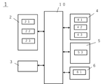
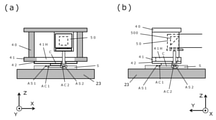
- FIG. 1 is a schematic view of a mounting device 1 according to an embodiment of the present invention.
- the mounting device mounts chip components on a board such as a wiring board, but the mounting device 1 in FIG. 1 is suitable for face-up mounting in which the electrode surface of the chip component and the electrode surface of the substrate are mounted in the same direction. It has a structure like that.
- the mounting device 1 includes a substrate stage 2, an elevating and pressurizing unit 3, a bonding head 4, a recognition mechanism 5, and a chip transfer means 6.
- the substrate stage 2 is composed of a stage movement control means 20 and a suction table 23.
- the suction table 23 sucks and holds the substrate arranged on the surface, and the suction table 23 can be moved in the in-plane direction of the substrate surface while holding the substrate by the stage movement control means 20. be.
- the stage movement control means 20 is provided on the base 200 with the Y-direction stage movement control means 22 capable of linearly moving the suction table 23 in the Y direction and the Y-direction stage movement control means 22 capable of linearly moving in the X direction. It is configured by the X-direction stage movement control means 21.
- the Y-direction movement control means 22 has a suction table 23 mounted on a movable portion arranged on the slide rail, and the movable portion is moved and position-controlled by the Y-direction servo 221.
- the X-direction movement control means 21 has a Y-direction movement control means 22 mounted on a movable portion arranged on the slide rail, and the movable portion is moved and position-controlled by the X-direction servo 211.
- the elevating and pressurizing unit 3 is fixed to a portal frame (not shown), the vertical drive shaft is provided in the direction perpendicular to the suction table 23, and the mounting head 4 is connected to the vertical drive shaft.
- the elevating and pressurizing unit 3 has a function of driving the mounting head 4 up and down and applying a pressing force according to the setting. Further, in the mounting device 1, since the elevating and pressurizing unit 3 is supported from two directions and is linearly connected to the mounting head 4, it is difficult to apply a lateral force to the mounting head 4 during pressurization. There is.
- the mounting head 4 holds the chip component C and crimps it in a state parallel to the board (held on the suction table 23 of the board stage 2).
- the mounting head 4 includes a head main body 40, a heater unit 41, an attachment tool 42, and a tool position control means 43 as components.
- the head body 40 is connected to the elevating and pressurizing unit 3 via the tool position control means 43, and the heater unit 41 is fixedly arranged on the lower side.
- the heater unit 41 has a heat generating function and heats the chip component C via the attachment tool 42. Further, the heater unit 41 has a function of sucking and holding the attachment tool 42 by using the decompression flow path.
- the attachment tool 42 sucks and holds the chip component C, and is replaced according to the shape of the chip component C.
- the tool position control means 43 finely adjusts the position of the head body 40 in the in-plane direction with the vertical drive axis of the elevating and pressurizing unit 3 as a perpendicular line, and the attachment tool 42 and the attachment tool 42 respond accordingly.
- the position of the chip component C to be held (in the XY plane in the figure) is adjusted.
- the tool position control means 43 includes an X-direction tool position control means 431, a Y-direction tool position control means 432, and a tool rotation control means 433 as components.
- the tool rotation control means 433 adjusts the rotation direction of the head body 40
- the Y direction tool position control means 432 adjusts the Y direction position of the tool rotation control means 433, and the X direction tool position control is performed.
- the means 431 is configured to adjust the X-direction position of the Y-direction position control means, but the present invention is not limited to this, and the X-direction position and the Y-direction of the head body 40 (and the components below it) are not limited to this. It suffices if the position and rotation angle can be adjusted.
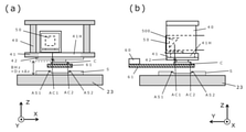
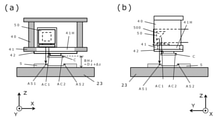
- FIG. 2 shows mainly the periphery of the head body 40 (front view in FIG. 2A and side view in FIG. 2B), but is shown in FIG. 27 in the face-up mounting of the present embodiment.
- the chip recognition mark AC chip recognition first mark AC1 and chip recognition second mark AC2
- the board is recognized at the diagonal reference position of the chip component mounting location on the substrate S electrode surface.
- Mark AS board recognition first mark AS1 and board recognition second mark AS2
- both of them face the direction of the mounting head 4.
- the mounting device 1 has a configuration in which the chip recognition mark AC can be observed through the mounting head 4, and the attachment tool 42 is formed of a transparent member or a through hole aligned with the position of the chip recognition mark AC is provided. It is provided. Further, it is necessary to use a transparent member or provide an opening for the heater portion 41 so that the chip recognition mark AC can be observed, and in the present embodiment, the through hole 41H is provided as shown in FIG.
- the through hole 41H may be provided according to the position of each chip recognition mark AC, but since it is not necessary to replace the chip component C depending on the shape, the hole shape may be such that the entire specification dimensional range can be accommodated. ..
- the mounting head 4 needs a space in which the image acquisition unit 50 of the recognition mechanism 5 can penetrate, and as shown in FIG. 2 in this embodiment.
- the head space 40V is provided in. That is, the head main body 40 has a structure composed of a side plate connected on the heater 41 and a top plate connecting both side plates.
- the recognition mechanism 5 acquires the position information of the chip recognition mark AC and / or the substrate recognition mark AS, which is focused and imaged through the mounting head 4 (through the attachment tool 42 and the heater unit 41). be.
- the recognition mechanism 5 includes an image capturing unit 50, an optical path 52, and an image pickup means 53 connected to the optical path 52 as components.
- the image capturing unit 50 is arranged above the recognition target on which the image pickup means 53 acquires an image, and the recognition target is housed in the field of view.
- the recognition mechanism 5 is configured to be able to move in the in-plane direction of the substrate S (and the chip component C) within the head space of 40 V by a drive mechanism (not shown). Further, it is desirable that the substrate S can be moved in the vertical direction (Z direction) so that the focal position can be adjusted.
- the mounting head 4 is moved in the direction perpendicular to the substrate S by the elevating and pressurizing unit 3, but this operation can be performed independently of the operation of the recognition mechanism 5. Therefore, it is necessary to design the head space 40V so that the recognition mechanism 5 that has entered the head space 40V does not interfere with the mounting head 4 even if the mounting head 4 moves in the vertical direction.
- the movable range of the image capturing unit 50 of the recognition mechanism 5 is not limited to the head space 40V, but moves away from the head space 40V and moves on the board S to acquire the position information of the board recognition mark AS. It is also possible to do.
- the tip transfer means 6 is composed of a transfer rail 60 and a chip slider 61, and the chip component C supplied from a chip supply unit (not shown) is held by the chip slider 61 and slid to directly below the attachment tool 42 to convey the tip component C. It is a thing.
- the chip supply unit arranges the chip component C at a fixed position on the chip slider 61. If necessary, the chip component C arranged on the chip slider 61 may recognize the arrangement position by a recognition mechanism (not shown). By controlling the positions of the chip slider 61 and the chip component C arranged on the chip slider 61 in this way, it is possible to deliver the chip component C within a predetermined range of the attachment tool 42. After the attachment tool 42 holds the chip component C, the chip slider 61 that has released the holding of the chip component C moves to the retracted position.
- the mounting device 1 includes a substrate stage 2, an elevating and pressurizing unit 3, a mounting head 4, a recognition mechanism 5, and a control unit 10 connected to a chip transfer means 6.
- the control unit 10 has a CPU and a storage device as main components in substance, and an interface is interposed with each device as needed. Further, by incorporating a program, the control unit 10 can perform an operation using the acquired data and output according to the operation result. Further, it is desirable to have a function of recording acquired data and calculation results and using them as data for new calculation.
- the control unit 10 is connected to the substrate stage 2 and controls the operation of the X-direction stage movement control means 21 and the Y-direction stage movement control means 22 to control the in-plane movement of the suction table 23. Further, the control unit 10 controls the suction table 23 to control the suction holding and release of the substrate S.
- the control unit 10 has a function of connecting to the elevating and pressurizing unit 3 to control the position of the mounting head 4 in the vertical direction (Z direction) and to control the pressing force when the chip component C is crimped to the substrate S. is doing.
- the control unit 10 is connected to the mounting head 4, and the suction holding and releasing of the chip component C by the attachment tool 42, the heating temperature of the heater unit 41, and the head body 40 (and the heater unit 41, the attachment tool 42) in the XY plane. It has a function of controlling the position by using the tool position control means 43.
- the control unit 10 is connected to the recognition mechanism 5 and has a function of controlling driving in the horizontal (in the XY plane) direction and the vertical direction (Z direction) and controlling the image pickup means 53 to acquire image data. .. Further, the control unit 10 has an image processing function, and has a function of calculating the positions of the chip recognition mark AC and / and the substrate recognition mark AS from the image acquired by the image pickup means 53.
- the control unit 10 is connected to the chip transfer means 6 and has a function of controlling the position of the chip slider 61 that moves along the transfer rail 60.
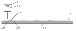
- FIG. 4 shows an example of the substrate S handled in the embodiment of the present invention.
- the board S has a plurality of mounting points SC, and each of the mounting points SC is provided with a board recognition first mark AS1 and a board recognition second mark AS2.
- the reference mark board reference mark AS0
- the board reference first mark AS01 and the board reference second mark AS02 may be provided, and the individual mounting points SC (and the board recognition mark AS) may be provided.
- the control unit 10 of the mounting device 1 has a function of calculating and storing the position information of each mounting location SC of the substrate S arranged on the suction table 23.
- An example thereof is shown in FIG. 5. While the suction table 23 holding the substrate S is moved by the stage moving means 20, each substrate recognition mark AS arranged on the substrate S is imaged and positioned by the recognition mechanism 5. It shows how the information is acquired, and the position information of each mounting location SC is calculated and stored. Further, when the board reference first mark AS01 and the board reference second mark AS02 are provided, the control unit 10 stores the map of the mounting location SC on the board S in advance so that the board reference first mark is provided.
- the recognition mechanism 5 may be moved.
- the chip component C is mounted on each mounting location SC.
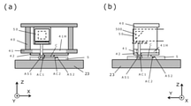
- FIG. 6 shows a mounting preparation process in which the attachment tool 42 of the mounting head 4 holds the chip component C and the mounting location SC for mounting the chip component C next to the substrate S is arranged directly under the mounting head 4. ..
- this mounting preparation step it is desirable to improve the position accuracy of the chip component C held by the attachment tool 42 and the position accuracy of the mounting location SC in order to shorten the time of the subsequent process.
- the stage movement control for controlling the position of the suction table 23 with high accuracy based on the position information of each mounting location SC obtained earlier. It is desirable to adopt the means 20.
- the mounting location SC of the board S is arranged with high accuracy directly under the mounting head 4. Therefore, in the preliminary alignment step to be performed next, only the position information of the chip component C is obtained by the recognition mechanism 5 on the premise that the mounting location SC of the board S exists within a predetermined range directly under the mounting head 4. ..
- FIG. 7 shows the state of the preliminary alignment process.
- the mounting head 4 is slightly raised during the preliminary alignment step. That is, assuming that the distance between the lower surface of the attachment tool 42 of the mounting head 4 with respect to the surface of the suction table 23 is the mounting head height BHZ, the mounting head height BHZ in the preliminary alignment step increases by ⁇ z from Dz in the mounting preparation step. Then, it becomes Dz + ⁇ z.
- the preliminary alignment step is performed with the chip component C held by the attachment tool 42, but since the recognition mechanism 5 observes only the chip recognition mark AC, the chip Even while the slider 61 is in the process of retracting, the position information of the chip component C can be obtained.
- the recognition mechanism 5 is moved in the XY plane so as to align the image capturing unit 50 with each other. Note that FIG. 9 shows an example in which the chip slider 61 is retracted at the stage of recognizing the chip recognition second mark AC2.
- the mounting location SC to be mounted next is arranged directly under the bonding head 4 within a predetermined accuracy from the position information of the mounting location SC acquired in advance at the stage of the preliminary alignment process. Therefore, it is also possible to determine the allowable range PAC in which the chip recognition mark AC of the chip component C should be located. Therefore, FIG. 10 shows the relationship between the chip recognition first mark AC1 acquired by the image pickup means 53 of the recognition means 5 and the allowable range PAC in which the chip recognition first mark AC is located at one position.
- the position information of the center of the chip recognition second mark AC2 is also acquired, and the chip component C with respect to the mounting location SC is obtained.
- the position is adjusted so that the chip recognition first mark AC1 is within the allowable range PAC as shown in FIG. 10 (b).
- the weight load is usually smaller when the attachment tool 42 is moved than the suction table 23, it is desirable to adjust the position on the mounting head 4 side in the preliminary alignment.
- the preliminary alignment process is important when the chip parts are embedded and mounted in the ended bed board (board with built-in parts) as shown in FIG. 27. That is, in many cases, there is no margin in the opening area of the recess with respect to the mounting location SC, and the mounting head 4 is in a state where the outer edge EC of the chip component C is outside the edge EB of the recess as shown in FIG. 11A.
- the chip component C comes into contact with the surface of the substrate S outside the recess, and attempts to lower the mounting head 4 from this state to a height at which precision alignment described later is performed (FIG. 11 (b)), the chip component Causes troubles such as damage to C.
- the mounting head 4 is lowered by the elevating and pressurizing unit 3.
- the chip component C is brought as close as possible to the substrate S so as not to come into contact with the substrate S, and the circuit is stopped.
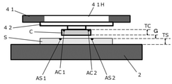
- the upper surface of the chip component C having the chip recognition first mark AC1 (and the chip recognition second mark AC2) and the upper surface of the substrate S having the substrate recognition first mark AS1 (and the substrate recognition second mark AS2) are formed. It is desirable that the vertical distance dS enters the depth of field of the recognition mechanism 5. Therefore, the conditions under which the vertical distance dS enters the depth of field of the recognition mechanism 5 will be described below.
- the vertical distance dS shown in FIG. 8 the distance (gap) G to the joint surface on which the chip component C of the substrate S is mounted, the thickness TC of the chip component C, and the depth DSC of the recess of the substrate S.
- the relationship can be expressed by the following equation (1).
- dS G + TC-DSC ⁇ ⁇ ⁇ ⁇ ⁇ ⁇ (1)
- “+ TC-DSC” is smaller than the thickness TC of the chip component C, which is usually 100 ⁇ m or less, and is several tens of ⁇ m or less. Further, when the chip component C is completely embedded in the substrate S, the value is zero or less. Therefore, if the chip component C can stop the descent of the mounting head 4 and reduce the gap G just before the chip component C comes into contact with the bottom surface of the recess of the substrate S, the chip recognition first mark AC1 and the substrate recognition first can be made within the depth of field. It is possible to accommodate the mark AS1 (or the chip recognition second mark AC2 and the substrate recognition second mark AS2).
- the control unit 10 of the mounting device 1 measures the surface height of the stage 2 (or the surface height of the substrate S) and the height of the mounting head 4 by a displacement sensor 7 (not shown), and the thickness of the chip component.
- the gap G is calculated using design values such as the thickness TS of the TC and the substrate S and the depth DSC of the recess, and the descent of the mounting head 4 is stopped at a height satisfying the condition of the equation (4).
- the gap G is set to a value exceeding zero in the equation (4), it is desirable that the gap G is several ⁇ m or more due to the relative movement of the chip component C and the substrate S for alignment.
- the actual values of the thickness TC of the chip component C, the thickness TS of the substrate S, the thickness of the thermosetting adhesive, and the depth DSC of the recesses have some variations with respect to the design values, so these variations are also taken into consideration. It is desirable to do.
- the displacement sensor 7 obtains the vertical distance of the surface of the substrate S with respect to the bonding head 4 (the lower surface of the attachment tool 42), and for that purpose, it is preferable to fix the displacement sensor 7 to the bonding head 4, but the displacement sensor 7 is limited to this. It may be fixed to the image capture unit 50 or the like instead of the object.
- FIG. 12 shows a state in which the position information of the substrate recognition second mark AS2 and the chip recognition second mark AC2 is acquired in a state where the head is lowered after the preliminary positioning is performed in the state of FIG. Is.
- the control unit 10 controls the driving means of the recognition mechanism 5 and moves the recognition mechanism 5 to the state shown in FIG. 13 to acquire the position information of the substrate recognition first mark AS1 and the chip recognition first mark AC1.
- FIG. 14 is a partially enlarged view of FIG. 13 (a).
- the substrate recognition first mark AS1 and the chip recognition first mark AC1 can be simultaneously imaged in the depth of field DOF.
- the vertical distance dS between the upper surface of the chip component C having the chip recognition first mark AC1 and the upper surface of the substrate S having the substrate recognition first mark AS1 is the depth of field of the image pickup means 53.
- the gap G is such that it is below the DOF.
- the image pickup means 53 can clearly image both the substrate recognition first mark AS1 and the chip recognition first mark AC1.
- both the substrate recognition second mark AS2 and the chip recognition second mark AC2 are clearly imaged by the image pickup means 53, so that the control unit 10 has the substrate recognition second mark AS2 and the chip.
- the relative position of the recognition second mark AC2 can be known accurately.
- the relative position information of the board recognition first mark AS1 and the chip recognition first mark AC1 obtained in the state of FIG. 13 and the board recognition second mark AS2 and the chip recognition second mark obtained in the state of FIG. 12 The relative position information of AC2 is used to align the substrate S and the chip component C. That is, first, the control unit 10 first obtains the substrate S and the chip component C from the relative position information of the board recognition first mark AS1 and the chip recognition first mark AC1 and the relative position information of the board recognition second mark AS2 and the chip recognition second mark AC2. Calculate the amount of positional deviation from and.
- the correction movement amount of the substrate S and the chip component C in the substrate surface for correcting the positional deviation amount is calculated, controlled by the control unit 10, and the substrate stage 2 and / or the mounting head 4 is placed in the substrate surface ( Driven in the XY and ⁇ ) directions, precise alignment is performed so that the amount of misalignment between the substrate S and the chip component C is within the allowable range.
- the chip component C is thermocompression bonded to the substrate S.
- the control unit 10 lowers the mounting head 4, brings the chip component C into close contact with the substrate S, and mounts the chip component C under a predetermined pressure (FIG. 16).
- the descending distance of the mounting head 4 is the gap G, but the gap G shown in the equation (7) is about several ⁇ m to several tens of ⁇ m. Therefore, the position accuracy obtained in the alignment process is maintained in the mounting process, and high-precision mounting is realized.
- thermosetting adhesive between the substrate S and the chip component C is heated by the heater portion 41 of the mounting head 4, so that the chip component C is fixed to the substrate S.
- the mounting head 4 releases the adsorption and holding of the chip component C and rises, and the mounting process is completed.
- 100% mounting position accuracy measurement is accompanied by an increase in cost. It can be substituted without any. That is, the relative position information acquisition of the board recognition first mark AS1 and the chip recognition first mark AC1 performed in FIG. 13 and the relative position information acquisition of the board recognition second mark AS2 and the chip recognition second mark AC2 performed in FIG.
- the crimping process as shown in FIGS. 17 and 18, it is possible to obtain position information with respect to the substrate S in the crimping process for each chip component C, that is, mounting accuracy.
- the mounting position accuracy can be measured within the time required for the crimping process, and the mounting tact time can be not affected. Is.
- the crimping process is completed, and if there is a chip component C to be newly mounted, the mounting preparation process is started.
- the tool position control means 43 is arranged in the preliminary alignment step. Since it is rarely operated and only the accuracy is confirmed, the tact time is shortened and the mounting device is excellent in productivity.
- the positional deviation does not deviate from the allowable range unless there is an abnormality in each mechanism, only the device trouble determination may be performed. In such a case, it may be performed. It may be sufficient to only acquire the position information of either the chip recognition first mark AC1 or the chip recognition second mark AC2.
- the position information of only the chip component recognition mark AC is assumed on the premise that the mounting location SC of the board S is arranged under the mounting head 4 with predetermined accuracy at the time of preliminary alignment.
- the position information of the substrate recognition mark AS is acquired even at the time of preliminary alignment.
- the recognition mechanism 5 has an image acquisition unit 50, an optical system (common) 51, an optical path 52a and an optical path 52b branched into two from the optical system 51 with a common optical axis, and an optical path 52b.
- the image pickup means 53a connected to the optical path 52a and the image pickup means 53b connected to the optical path 52b are constituent elements.
- the focal positions of the image pickup means 53a and the focus positions of the image pickup means 53b are different from each other.
- the optical system (common) 51 has a function of changing the direction of the optical path by the reflecting means 500 and the reflecting means 520, and the optical path is branched by the half mirror 511.
- the optical system 52a and the optical system 52b may have an optical lens and may have a function of enlarging an image in order to obtain high resolution.
- the control unit 10 holds the board S on the board stage 2 and holds the chip component C on the mounting head 4.
- the substrate S is arranged within a predetermined range of the substrate stage 2, and the chip component C is held at a predetermined in-plane position on the lower surface of the attachment tool 42. That is, the chip component C and the substrate S are roughly aligned. Therefore, through the through hole 41H of the heater 41 and the attachment tool 42, all of the board recognition first mark AS1, the board recognition second mark AS2, the chip recognition first mark AC1, and the chip recognition second mark AC2 are mounted heads. It is in an observable state through 4.
- the substrate S and the chip component C are in a state where it is difficult to simultaneously fit both recognition marks within the depth of field due to the difference in height between the substrate recognition mark AS and the chip recognition mark AC.
- the substrate recognition mark and the chip recognition mark are observed by different imaging means having different focal lengths.
- FIG. 22 is a partially enlarged view of FIG. 20 (a).
- the height reference is the surface of the adsorption table 23.
- dS which is the vertical distance between the upper surface of the chip component C having the chip recognition first mark AC1 and the upper surface of the substrate S having the substrate recognition first mark AS1
- TS the thickness of the substrate S and (the lower surface of the attachment tool 42).
- BHz Dz + ⁇ z ... (6)
- dS Dz + ⁇ z-TS ... (7)
- Dz is about 10 mm because it is larger than the thickness of the chip slider 61 on which the chip component C is mounted, and ⁇ z is 1 mm or more and 2 mm or less as described above, whereas the thickness TS of the substrate S is general. Since it is 2 mm or less, dS is about 10 mm.
- the depth of field needs to be around 10 mm.
- the substrate recognition mark AS and the chip recognition mark AC are individually observed by imaging means having different focal lengths.
- the image pickup means 53a and the image pickup means 53b shown in FIG. 19 (b) are obtained.
- One of them focuses on the substrate recognition first mark AS1 and takes an image
- the other focuses on the chip recognition first mark AC1 and takes an image.
- the image pickup means 53a images the substrate recognition first mark AS1 and the image pickup means 53b captures the chip recognition first mark AC1 will be described.
- the image pickup means 53a and the image pickup means 53b and the optical system 52a and the optical system 52b have the same specifications such as the number of image pickup elements and the optical lens magnification, and the optical path length from the substrate recognition first mark AS1 to the image pickup means 53a. It is desirable that the optical path lengths from the chip recognition first mark AC1 to the image pickup means 53b are equal to each other.
- the image pickup means 53a obtains an image focused on the substrate recognition first mark AS1 as shown in FIG. 23 (a), and the image pickup means 53b obtains a chip recognition as shown in FIG. 23 (b).
- An image focused on the first mark AC1 is obtained.
- the image focused on the substrate recognition first mark AS1 and the chip recognition first mark AC1 can be simultaneously obtained via a common optical axis path.
- the relative position information of the substrate recognition first mark AS1 and the chip recognition first mark AC1 can be obtained.
- the control unit 10 controls the driving means of the recognition mechanism 5, and the image acquisition unit 50 is shown in FIG.
- the substrate recognition second mark AS2 and the chip recognition second mark AC2 are arranged at positions within the same field of view. At that time, if the movement is in the in-plane direction of the substrate (XY), the recognition mechanism 5 is maintained in a state of being in focus on each of the substrate recognition mark and the chip recognition mark without adjusting the position in the vertical direction (Z direction). ..
- the image pickup means 53a obtains an image in focus on the substrate recognition second mark AS12
- the image pickup means 53b obtains an image in focus on the chip recognition second mark AC2.
- the image focused on the substrate recognition first mark AS1 and the chip recognition first mark AC1 can be simultaneously obtained via a common optical axis path.
- the relative position information of the substrate recognition second mark AS2 and the chip recognition second mark AC2 can be obtained.
- the control unit 10 first obtains the substrate S and the chip component C from the relative position information of the board recognition first mark AS1 and the chip recognition first mark AC1 and the relative position information of the board recognition second mark AS2 and the chip recognition second mark AC2. Calculate the amount of positional deviation from and.
- the amount of misalignment exceeds the permissible range
- the amount of correction movement of the substrate S and the chip component C in the substrate surface for correcting the misalignment is calculated, and the substrate stage 2 and / or the mounting head 4 is driven in the in-plane (XY) direction of the substrate, the position is adjusted so that the amount of positional deviation between the substrate S and the chip component C is within the allowable range, and the preliminary alignment is completed.
- either the image pickup means 53a or the image pickup means 53b may be used as the image pickup means, but the image pickup means for observing the substrate recognition first mark AS1 (and the substrate recognition second mark AS2) is mounted. It is preferable because it is not necessary to change the focus even if the head 4 is lowered.
- FIG. 24 (a) Although an example of performing embedded mounting as shown in FIG. 27 by using the mounting device 1 of the embodiment shown in FIG. 1 or a modified example thereof (FIG. 19) has been described above, the present invention has been described in FIG. 24 (a). As described above, it can also be applied to the case where the chip component C is mounted on the mounting location SC of the substrate S having no recess as shown in FIG. 24 (b). In this case, since the board S is not mounted in the recess, both the board recognition first mark AS1 and the chip recognition first mark AC1 (and the board recognition second mark AS2 and the chip recognition second) are performed at the stage of the precision alignment process. Since both of the mark AC2) need to be in the same field of view of the imaging means, the need for preliminary alignment is reduced.
- the DSC of the equation (7) is set to zero. 0 ⁇ G ⁇ DOF-TC ... (8) It is necessary to obtain a gap G that satisfies the condition. That is, it is possible to mount using a thin chip component such that the thickness TC of the chip component C is smaller than the depth of field DOF.
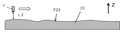
- the measurement may be performed using the displacement sensor 7, but the in-plane distribution of the surface height of the substrate stage 2 or the surface height of the substrate S may be measured. It may be grasped in advance, and the height of the mounting head 4 for each alignment step may be slightly modified based on this height distribution. By doing so, the time from the preliminary alignment step to the alignment step can be shortened.
- the displacement sensor 7 set to the reference height is used, and the substrate stage 2 is placed in the XY plane with respect to the displacement sensor 7.
- the surface height may be measured while moving relative to each other in the direction.
- FIG. 26 shows an example of measuring the height distribution (Z direction) of the surface F2 of the substrate stage 2 by the displacement sensor 7, and the substrate stage 2 is used with the displacement sensor 7 having a constant height (Z direction). Is shown to measure the Z-direction distance LZ to the surface F2 while relatively moving in the XY direction.
- the present invention is applied to the face-up mounting on the premise that the chip recognition mark is given to the electrode surface side of the chip component C is described, but the chip recognition is described on the side opposite to the electrode surface.
- the present invention can be applied to face-down mounting.
Landscapes
- Engineering & Computer Science (AREA)
- Manufacturing & Machinery (AREA)
- Microelectronics & Electronic Packaging (AREA)
- Operations Research (AREA)
- Supply And Installment Of Electrical Components (AREA)
- Wire Bonding (AREA)
- Die Bonding (AREA)
Priority Applications (5)
| Application Number | Priority Date | Filing Date | Title |
|---|---|---|---|
| CN202180048846.0A CN115836383A (zh) | 2020-07-13 | 2021-07-08 | 安装装置及安装方法 |
| JP2022536302A JPWO2022014451A1 (https=) | 2020-07-13 | 2021-07-08 | |
| JP2022151400A JP7293477B2 (ja) | 2020-07-13 | 2022-09-22 | 実装装置 |
| JP2022151474A JP7417684B2 (ja) | 2020-07-13 | 2022-09-22 | 実装装置 |
| US18/152,478 US12347803B2 (en) | 2020-07-13 | 2023-01-10 | Mounting device and mounting method |
Applications Claiming Priority (4)
| Application Number | Priority Date | Filing Date | Title |
|---|---|---|---|
| JP2020119622 | 2020-07-13 | ||
| JP2020-119622 | 2020-07-13 | ||
| JP2021061465 | 2021-03-31 | ||
| JP2021-061465 | 2021-03-31 |
Related Child Applications (1)
| Application Number | Title | Priority Date | Filing Date |
|---|---|---|---|
| US18/152,478 Continuation US12347803B2 (en) | 2020-07-13 | 2023-01-10 | Mounting device and mounting method |
Publications (1)
| Publication Number | Publication Date |
|---|---|
| WO2022014451A1 true WO2022014451A1 (ja) | 2022-01-20 |
Family
ID=79554833
Family Applications (1)
| Application Number | Title | Priority Date | Filing Date |
|---|---|---|---|
| PCT/JP2021/025715 Ceased WO2022014451A1 (ja) | 2020-07-13 | 2021-07-08 | 実装装置および実装方法 |
Country Status (4)
| Country | Link |
|---|---|
| US (1) | US12347803B2 (https=) |
| JP (3) | JPWO2022014451A1 (https=) |
| CN (1) | CN115836383A (https=) |
| WO (1) | WO2022014451A1 (https=) |
Cited By (3)
| Publication number | Priority date | Publication date | Assignee | Title |
|---|---|---|---|---|
| WO2023157061A1 (ja) * | 2022-02-15 | 2023-08-24 | 株式会社新川 | 検査装置、実装装置、検査方法、及びプログラム |
| WO2025204579A1 (ja) * | 2024-03-28 | 2025-10-02 | 東レエンジニアリング株式会社 | 実装装置 |
| WO2025204573A1 (ja) * | 2024-03-28 | 2025-10-02 | 東レエンジニアリング株式会社 | 実装装置および位置合わせ方法 |
Families Citing this family (2)
| Publication number | Priority date | Publication date | Assignee | Title |
|---|---|---|---|---|
| WO2025141803A1 (ja) * | 2023-12-27 | 2025-07-03 | 株式会社Fuji | 対基板作業機、および補正データ作成方法 |
| KR102914700B1 (ko) * | 2025-01-14 | 2026-01-19 | 주식회사 브이디 | 정밀 프레스 장치 |
Citations (4)
| Publication number | Priority date | Publication date | Assignee | Title |
|---|---|---|---|---|
| JP2000276233A (ja) * | 1999-03-24 | 2000-10-06 | Moritex Corp | 位置ずれ検出装置及びそれを用いた位置決め装置 |
| JP2008109057A (ja) * | 2006-10-27 | 2008-05-08 | Toray Eng Co Ltd | 半導体チップの実装装置及び実装方法 |
| JP2010283010A (ja) * | 2009-06-02 | 2010-12-16 | Adwelds:Kk | アライメント装置、この装置を備えた実装装置およびアライメント方法 |
| WO2020044580A1 (ja) * | 2018-08-31 | 2020-03-05 | ボンドテック株式会社 | 部品実装システムおよび部品実装方法 |
Family Cites Families (10)
| Publication number | Priority date | Publication date | Assignee | Title |
|---|---|---|---|---|
| JPWO2003041478A1 (ja) * | 2001-11-05 | 2005-03-03 | 東レエンジニアリング株式会社 | 実装装置および実装方法 |
| JP4048896B2 (ja) * | 2002-09-30 | 2008-02-20 | ソニー株式会社 | ボンディング装置 |
| JP5245209B2 (ja) * | 2006-04-24 | 2013-07-24 | ソニー株式会社 | 半導体装置及びその製造方法 |
| JP4840862B2 (ja) * | 2006-08-29 | 2011-12-21 | 東レエンジニアリング株式会社 | 実装装置のチップ供給方法、及びその実装装置 |
| JP4825171B2 (ja) * | 2007-06-08 | 2011-11-30 | 株式会社新川 | ボンディング装置用撮像装置及び撮像方法 |
| JP2015130414A (ja) * | 2014-01-08 | 2015-07-16 | 東レエンジニアリング株式会社 | 自動ボンディング装置 |
| JP6390925B2 (ja) * | 2016-05-11 | 2018-09-19 | パナソニックIpマネジメント株式会社 | 部品実装装置 |
| JP6849468B2 (ja) * | 2017-02-13 | 2021-03-24 | ファスフォードテクノロジ株式会社 | 半導体製造装置および半導体装置の製造方法 |
| JP2019102771A (ja) * | 2017-12-08 | 2019-06-24 | アスリートFa株式会社 | 電子部品実装装置及び電子部品実装方法 |
| JP7112341B2 (ja) * | 2019-01-23 | 2022-08-03 | 東レエンジニアリング株式会社 | 実装装置および実装方法 |
-
2021
- 2021-07-08 CN CN202180048846.0A patent/CN115836383A/zh active Pending
- 2021-07-08 WO PCT/JP2021/025715 patent/WO2022014451A1/ja not_active Ceased
- 2021-07-08 JP JP2022536302A patent/JPWO2022014451A1/ja active Pending
-
2022
- 2022-09-22 JP JP2022151474A patent/JP7417684B2/ja active Active
- 2022-09-22 JP JP2022151400A patent/JP7293477B2/ja active Active
-
2023
- 2023-01-10 US US18/152,478 patent/US12347803B2/en active Active
Patent Citations (4)
| Publication number | Priority date | Publication date | Assignee | Title |
|---|---|---|---|---|
| JP2000276233A (ja) * | 1999-03-24 | 2000-10-06 | Moritex Corp | 位置ずれ検出装置及びそれを用いた位置決め装置 |
| JP2008109057A (ja) * | 2006-10-27 | 2008-05-08 | Toray Eng Co Ltd | 半導体チップの実装装置及び実装方法 |
| JP2010283010A (ja) * | 2009-06-02 | 2010-12-16 | Adwelds:Kk | アライメント装置、この装置を備えた実装装置およびアライメント方法 |
| WO2020044580A1 (ja) * | 2018-08-31 | 2020-03-05 | ボンドテック株式会社 | 部品実装システムおよび部品実装方法 |
Cited By (4)
| Publication number | Priority date | Publication date | Assignee | Title |
|---|---|---|---|---|
| WO2023157061A1 (ja) * | 2022-02-15 | 2023-08-24 | 株式会社新川 | 検査装置、実装装置、検査方法、及びプログラム |
| JP7336814B1 (ja) * | 2022-02-15 | 2023-09-01 | 株式会社新川 | 検査装置、実装装置、検査方法、及びプログラム |
| WO2025204579A1 (ja) * | 2024-03-28 | 2025-10-02 | 東レエンジニアリング株式会社 | 実装装置 |
| WO2025204573A1 (ja) * | 2024-03-28 | 2025-10-02 | 東レエンジニアリング株式会社 | 実装装置および位置合わせ方法 |
Also Published As
| Publication number | Publication date |
|---|---|
| US20230163096A1 (en) | 2023-05-25 |
| JP2023051804A (ja) | 2023-04-11 |
| JP2023058432A (ja) | 2023-04-25 |
| JP7417684B2 (ja) | 2024-01-18 |
| JP7293477B2 (ja) | 2023-06-19 |
| JPWO2022014451A1 (https=) | 2022-01-20 |
| CN115836383A (zh) | 2023-03-21 |
| US12347803B2 (en) | 2025-07-01 |
Similar Documents
| Publication | Publication Date | Title |
|---|---|---|
| JP7417684B2 (ja) | 実装装置 | |
| CN113348538B (zh) | 安装装置和安装方法 | |
| JP7829772B2 (ja) | 実装装置および実装方法 | |
| CN112218517B (zh) | 安装装置 | |
| JP2004128384A (ja) | 部品実装装置および部品実装方法 | |
| CN118511261A (zh) | 定位装置以及使用该定位装置的安装装置 | |
| JP7757255B2 (ja) | 実装装置 | |
| US20260020211A1 (en) | Mounting device | |
| JP2006114841A (ja) | ボンディング装置 | |
| JP7013400B2 (ja) | 実装装置および実装方法 | |
| JPH11176883A (ja) | バンプ付電子部品の熱圧着装置および熱圧着方法 | |
| WO2024203421A1 (ja) | ツールスライダ、チップスライダおよび実装装置 | |
| WO2025154397A1 (ja) | 実装装置 |
Legal Events
| Date | Code | Title | Description |
|---|---|---|---|
| 121 | Ep: the epo has been informed by wipo that ep was designated in this application |
Ref document number: 21842925 Country of ref document: EP Kind code of ref document: A1 |
|
| ENP | Entry into the national phase |
Ref document number: 2022536302 Country of ref document: JP Kind code of ref document: A |
|
| NENP | Non-entry into the national phase |
Ref country code: DE |
|
| 122 | Ep: pct application non-entry in european phase |
Ref document number: 21842925 Country of ref document: EP Kind code of ref document: A1 |