WO2022004084A1 - 半導体装置 - Google Patents
半導体装置 Download PDFInfo
- Publication number
- WO2022004084A1 WO2022004084A1 PCT/JP2021/014138 JP2021014138W WO2022004084A1 WO 2022004084 A1 WO2022004084 A1 WO 2022004084A1 JP 2021014138 W JP2021014138 W JP 2021014138W WO 2022004084 A1 WO2022004084 A1 WO 2022004084A1
- Authority
- WO
- WIPO (PCT)
- Prior art keywords
- region
- trench portion
- trench
- contact
- semiconductor device
- Prior art date
- Legal status (The legal status is an assumption and is not a legal conclusion. Google has not performed a legal analysis and makes no representation as to the accuracy of the status listed.)
- Ceased
Links
Images




Classifications
-
- H—ELECTRICITY
- H10—SEMICONDUCTOR DEVICES; ELECTRIC SOLID-STATE DEVICES NOT OTHERWISE PROVIDED FOR
- H10D—INORGANIC ELECTRIC SEMICONDUCTOR DEVICES
- H10D8/00—Diodes
- H10D8/422—PN diodes having the PN junctions in mesas
-
- H—ELECTRICITY
- H10—SEMICONDUCTOR DEVICES; ELECTRIC SOLID-STATE DEVICES NOT OTHERWISE PROVIDED FOR
- H10D—INORGANIC ELECTRIC SEMICONDUCTOR DEVICES
- H10D12/00—Bipolar devices controlled by the field effect, e.g. insulated-gate bipolar transistors [IGBT]
- H10D12/411—Insulated-gate bipolar transistors [IGBT]
- H10D12/441—Vertical IGBTs
- H10D12/461—Vertical IGBTs having non-planar surfaces, e.g. having trenches, recesses or pillars in the surfaces of the emitter, base or collector regions
- H10D12/481—Vertical IGBTs having non-planar surfaces, e.g. having trenches, recesses or pillars in the surfaces of the emitter, base or collector regions having gate structures on slanted surfaces, on vertical surfaces, or in grooves, e.g. trench gate IGBTs
-
- H—ELECTRICITY
- H10—SEMICONDUCTOR DEVICES; ELECTRIC SOLID-STATE DEVICES NOT OTHERWISE PROVIDED FOR
- H10D—INORGANIC ELECTRIC SEMICONDUCTOR DEVICES
- H10D62/00—Semiconductor bodies, or regions thereof, of devices having potential barriers
- H10D62/10—Shapes, relative sizes or dispositions of the regions of the semiconductor bodies; Shapes of the semiconductor bodies
- H10D62/124—Shapes, relative sizes or dispositions of the regions of semiconductor bodies or of junctions between the regions
- H10D62/126—Top-view geometrical layouts of the regions or the junctions
- H10D62/127—Top-view geometrical layouts of the regions or the junctions of cellular field-effect devices, e.g. multicellular DMOS transistors or IGBTs
-
- H—ELECTRICITY
- H10—SEMICONDUCTOR DEVICES; ELECTRIC SOLID-STATE DEVICES NOT OTHERWISE PROVIDED FOR
- H10D—INORGANIC ELECTRIC SEMICONDUCTOR DEVICES
- H10D62/00—Semiconductor bodies, or regions thereof, of devices having potential barriers
- H10D62/10—Shapes, relative sizes or dispositions of the regions of the semiconductor bodies; Shapes of the semiconductor bodies
- H10D62/13—Semiconductor regions connected to electrodes carrying current to be rectified, amplified or switched, e.g. source or drain regions
- H10D62/133—Emitter regions of BJTs
-
- H—ELECTRICITY
- H10—SEMICONDUCTOR DEVICES; ELECTRIC SOLID-STATE DEVICES NOT OTHERWISE PROVIDED FOR
- H10D—INORGANIC ELECTRIC SEMICONDUCTOR DEVICES
- H10D62/00—Semiconductor bodies, or regions thereof, of devices having potential barriers
- H10D62/10—Shapes, relative sizes or dispositions of the regions of the semiconductor bodies; Shapes of the semiconductor bodies
- H10D62/17—Semiconductor regions connected to electrodes not carrying current to be rectified, amplified or switched, e.g. channel regions
- H10D62/393—Body regions of DMOS transistors or IGBTs
-
- H—ELECTRICITY
- H10—SEMICONDUCTOR DEVICES; ELECTRIC SOLID-STATE DEVICES NOT OTHERWISE PROVIDED FOR
- H10D—INORGANIC ELECTRIC SEMICONDUCTOR DEVICES
- H10D64/00—Electrodes of devices having potential barriers
- H10D64/01—Manufacture or treatment
- H10D64/017—Manufacture or treatment using dummy gates in processes wherein at least parts of the final gates are self-aligned to the dummy gates, i.e. replacement gate processes
-
- H—ELECTRICITY
- H10—SEMICONDUCTOR DEVICES; ELECTRIC SOLID-STATE DEVICES NOT OTHERWISE PROVIDED FOR
- H10D—INORGANIC ELECTRIC SEMICONDUCTOR DEVICES
- H10D64/00—Electrodes of devices having potential barriers
- H10D64/111—Field plates
- H10D64/117—Recessed field plates, e.g. trench field plates or buried field plates
-
- H—ELECTRICITY
- H10—SEMICONDUCTOR DEVICES; ELECTRIC SOLID-STATE DEVICES NOT OTHERWISE PROVIDED FOR
- H10D—INORGANIC ELECTRIC SEMICONDUCTOR DEVICES
- H10D64/00—Electrodes of devices having potential barriers
- H10D64/20—Electrodes characterised by their shapes, relative sizes or dispositions
- H10D64/27—Electrodes not carrying the current to be rectified, amplified, oscillated or switched, e.g. gates
- H10D64/311—Gate electrodes for field-effect devices
- H10D64/411—Gate electrodes for field-effect devices for FETs
- H10D64/511—Gate electrodes for field-effect devices for FETs for IGFETs
- H10D64/512—Disposition of the gate electrodes, e.g. buried gates
- H10D64/513—Disposition of the gate electrodes, e.g. buried gates within recesses in the substrate, e.g. trench gates, groove gates or buried gates
-
- H—ELECTRICITY
- H10—SEMICONDUCTOR DEVICES; ELECTRIC SOLID-STATE DEVICES NOT OTHERWISE PROVIDED FOR
- H10D—INORGANIC ELECTRIC SEMICONDUCTOR DEVICES
- H10D64/00—Electrodes of devices having potential barriers
- H10D64/20—Electrodes characterised by their shapes, relative sizes or dispositions
- H10D64/23—Electrodes carrying the current to be rectified, amplified, oscillated or switched, e.g. sources, drains, anodes or cathodes
-
- H—ELECTRICITY
- H10—SEMICONDUCTOR DEVICES; ELECTRIC SOLID-STATE DEVICES NOT OTHERWISE PROVIDED FOR
- H10D—INORGANIC ELECTRIC SEMICONDUCTOR DEVICES
- H10D8/00—Diodes
- H10D8/80—PNPN diodes, e.g. Shockley diodes or break-over diodes
Definitions
- the present invention relates to a semiconductor device.
- Patent Document 1 describes that "improving characteristics such as saturation current in a semiconductor device”.
- Patent Document 1 Japanese Unexamined Patent Publication No. 2018-195798
- Patent Document 2 International Publication No. 2018/0520108 Pamphlet
- a semiconductor device including a gate trench portion and a first trench portion adjacent to the gate trench portion.
- the semiconductor device is provided with a first conductive type drift region provided on the semiconductor substrate, a second conductive type base region provided above the drift region, and above the base region, and has a doping concentration higher than that of the drift region. It may be provided with a high first conductive type emitter region and a second conductive type contact region provided above the base region and having a higher doping concentration than the base region.
- the contact region may be provided below the lower end of the emitter region.
- the contact area may be in contact with the first trench portion.
- the contact region may be separated from the gate trench portion.
- the contact region may be separated from the gate trench portion by 0.6 ⁇ m or more in the trench arrangement direction.
- the contact region may be provided on the front surface of the semiconductor substrate on the side wall of the first trench portion.
- the semiconductor device may include an interlayer insulating film provided above the semiconductor substrate.
- the emitter region may be electrically connected to the emitter electrode through a contact hole provided through the interlayer insulating film.
- the emitter region may extend from the gate trench portion to the first trench portion side beyond the contact hole in the trench arrangement direction.
- the semiconductor device may include a first conductive type storage region having a higher doping concentration than the drift region between the drift region and the base region.
- the semiconductor device may include a plurality of gate trench portions and a plurality of first trench portions.
- the ratio of the number of the plurality of gate trench portions to the number of the plurality of first trench portions may be 1: 1.
- the semiconductor device may include a plurality of gate trench portions and a plurality of first trench portions.
- the ratio of the number of the plurality of gate trench portions to the number of the plurality of first trench portions may be 1: 2.
- the emitter region may extend from the gate trench portion to the dummy trench portion in the trench arrangement direction.
- the emitter region may be terminated without reaching the first trench portion.
- the emitter region may extend from the gate trench portion to the first trench portion in the trench arrangement direction.
- the contact region and the emitter region may be alternately provided in contact with each other in the trench extending direction of the gate trench portion.
- the first trench portion may be set to the emitter potential.
- the first trench portion may be set to the gate potential.
- the first trench portion may be a dummy trench.
- the emitter region may be in contact with the gate trench portion in the mesa portion and separated from the first trench portion.
- the contact region may be provided below the lower end of the emitter region on the first trench portion side in the mesa portion.
- the first trench portion may include a dummy gate trench portion that is set to the gate potential and does not contact the emitter region.
- the first trench portion may include a dummy trench portion set to the emitter potential.
- the emitter region may have a first emitter region in the mesa portion that is in contact with the gate trench portion and is separated from the first trench portion.
- the contact region may be provided below the lower end of the first emitter region on the first trench portion side in the mesa portion.
- the emitter region may further have a second emitter region in the mesa portion that is in contact with the first trench portion and is separated from the gate trench portion.
- the contact region may also be provided below the lower end of the second emitter region on the gate trench portion side in the mesa portion.
- the first emitter region and the second emitter region may be provided alternately in the trench extension direction of the gate trench portion.
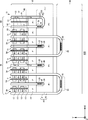
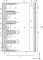
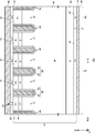
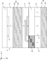
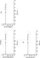
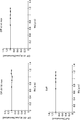
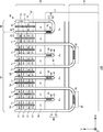
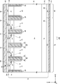
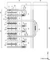
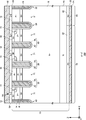
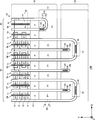
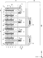
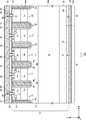
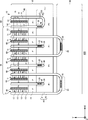
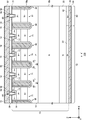
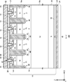
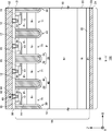
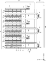
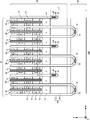
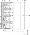
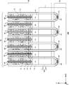
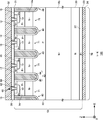
- the top view of the semiconductor device 100 is shown. It is an example of a'a'cross-sectional view in FIG. 1A. It is an example of the bb'cross-sectional view in FIG. 1A. An example of an enlarged cross-sectional view of the mesa portion 71 is shown. An example of a top view of a semiconductor device 100 having an unopened portion of a contact hole 54 is shown. An example of the simulation result of the static characteristic of the semiconductor device 100 is shown. An example of the simulation result of the on-characteristic of the semiconductor device 100 is shown. An example of the simulation result of the off characteristic of the semiconductor device 100 is shown. An example of the top view of the semiconductor device 100 is shown.
- FIG. 5A This is an example of a cross-sectional view taken along the line cc'in FIG. 5A.
- An example of the top view of the semiconductor device 100 is shown. It is an example of the dd'cross-sectional view in FIG. 6A.
- An example of the top view of the semiconductor device 100 which is a modification is shown.
- An example of the top view of the semiconductor device 100 is shown.
- An example of the top view of the semiconductor device 100 is shown.
- An example of the top view of the semiconductor device 100 is shown.
- FIG. 10A It is an example of the cross-sectional view of hh'in FIG. 10A. It is another example of the hh'cross-sectional view in FIG. 10A.
- An example of the top view of the semiconductor device 100 is shown. It is an example of the cross-sectional view of ii'in FIG. 11A. An example of the top view of the semiconductor device 100 is shown. It is an example of the cross-sectional view of jJ'in FIG. 12A. An example of the top view of the semiconductor device 100 is shown. It is an example of the cross-sectional view of kk'in FIG. 13A.
- one side in the direction parallel to the depth direction of the semiconductor substrate is referred to as "upper”, and the other side is referred to as “lower”.
- the front surface is referred to as the front surface and the other surface is referred to as the back surface.
- the directions of "top”, “bottom”, “front”, and “back” are not limited to the direction of gravity or the direction of mounting on a substrate or the like when mounting a semiconductor device.
- the plane parallel to the front surface of the semiconductor substrate is defined as the XY plane
- the direction forming a right-handed system with the X-axis and the Y-axis and the direction parallel to the depth direction of the semiconductor substrate is defined as the Z-axis. do.
- the first conductive type is N type and the second conductive type is P type, but the first conductive type may be P type and the second conductive type may be N type.
- the conductive types such as the substrate, the layer, and the region in each embodiment have opposite polarities.
- N or P the electron or hole is a large number of carriers in the layer or region marked with N or P, respectively.
- + and-attached to N and P mean that the doping concentration is higher and the doping concentration is lower than those of the unsigned layers and regions, respectively.
- FIG. 1A shows an example of a top view of the semiconductor device 100.
- the semiconductor device 100 of this example is a semiconductor chip including a transistor unit 70 and a diode unit 80.
- the semiconductor device 100 is a trench gate type RC-IGBT (Reverse Conducting Integrated Gate Bipolar Transistor) in which a plurality of trench portions are arranged.
- the plurality of trench portions are arranged in the X-axis direction and extend in the Y-axis direction.
- the transistor portion 70 is a region in which a collector region 22 provided on the back surface side of the semiconductor substrate 10 is projected onto the upper surface of the semiconductor substrate 10, which will be described later in FIG. 1B.
- the collector region 22 has a second conductive type.
- the collector area 22 of this example is a P + type as an example.
- the transistor unit 70 includes a transistor such as an IGBT.
- the diode portion 80 is a region in which the cathode region 82 provided on the back surface side of the semiconductor substrate 10 is projected onto the upper surface of the semiconductor substrate 10, which will be described later in FIG. 1B.
- the cathode region 82 has a first conductive type.
- the cathode region 82 of this example is N + type as an example.
- the diode section 80 includes a diode such as a freewheeling diode (FWD: Free Wheel Diode) provided adjacent to the transistor section 70 on the upper surface of the semiconductor substrate 10.
- FWD Free Wheel Diode
- FIG. 1A a region around the chip end portion on the edge side of the semiconductor device 100 is shown, and other regions are omitted.
- an edge termination structure portion is provided in a region on the negative side in the Y-axis direction.
- the edge terminal structure portion relaxes the electric field concentration on the upper surface side of the semiconductor substrate 10.
- the edge termination structure has, for example, a guard ring, a field plate, a resurf, and a structure in which these are combined.
- the negative edge in the Y-axis direction will be described, but the same applies to the other edges of the semiconductor device 100.
- the semiconductor substrate 10 may be a silicon substrate, a silicon carbide substrate, a nitride semiconductor substrate such as gallium nitride, or the like.
- the semiconductor substrate 10 of this example is a silicon substrate.
- the semiconductor device 100 of this example has a gate trench portion 40, a dummy trench portion 30, an emitter region 12, a base region 14, a contact region 15, and a well region 17 on the front surface of the semiconductor substrate 10. Be prepared. Further, the semiconductor device 100 of this example includes an emitter electrode 52 and a gate metal layer 50 provided above the front surface of the semiconductor substrate 10.
- the emitter electrode 52 is provided above the gate trench portion 40, the dummy trench portion 30, the emitter region 12, the base region 14, the contact region 15, and the well region 17. Further, the gate metal layer 50 is provided above the gate trench portion 40 and the well region 17.
- the emitter electrode 52 and the gate metal layer 50 are formed of a material containing metal.
- the emitter electrode 52 is formed of an aluminum, aluminum-silicon alloy, or aluminum-silicon-copper alloy.
- At least a partial region of the gate metal layer 50 may be formed of aluminum, aluminum-silicon alloy, or aluminum-silicon-copper alloy.
- the emitter electrode 52 and the gate metal layer 50 may have a barrier metal formed of titanium, a titanium compound, or the like in the lower layer of a region formed of aluminum or the like.
- the emitter electrode 52 and the gate metal layer 50 are provided separately from each other.
- the emitter electrode 52 and the gate metal layer 50 are provided above the semiconductor substrate 10 with the interlayer insulating film 38 interposed therebetween.
- the interlayer insulating film 38 is omitted in FIG. 1A.
- the interlayer insulating film 38 is provided with a contact hole 54, a contact hole 55, and a contact hole 56 penetrating.
- the contact hole 55 connects the gate metal layer 50 and the gate conductive portion in the gate trench portion 40 of the transistor portion 70.
- a plug made of tungsten or the like may be formed inside the contact hole 55.
- the contact hole 56 connects the emitter electrode 52 and the dummy conductive portion in the dummy trench portion 30.
- a plug made of tungsten or the like may be formed inside the contact hole 56.
- connection portion 25 electrically connects the front surface side electrode such as the emitter electrode 52 or the gate metal layer 50 to the semiconductor substrate 10.
- the connecting portion 25 is provided between the gate metal layer 50 and the gate conductive portion.
- the connecting portion 25 is also provided between the emitter electrode 52 and the dummy conductive portion.
- the connecting portion 25 is a conductive material such as polysilicon doped with impurities.
- the connecting portion 25 is polysilicon (N +) doped with N-type impurities.
- the connecting portion 25 is provided above the front surface of the semiconductor substrate 10 via an insulating film such as an oxide film.
- the gate trench portions 40 are arranged at predetermined intervals along a predetermined trench arrangement direction (X-axis direction in this example). As an example, the gate trench portions 40 are arranged at a trench spacing of 1.5 ⁇ m, but the trench spacing is not limited to this spacing.
- the gate trench portion 40 of this example includes two stretching portions 41 that are parallel to the front surface of the semiconductor substrate 10 and stretched along a trench stretching direction (Y-axis direction in this example) perpendicular to the trench arrangement direction. It may have a connecting portion 43 connecting the two stretched portions 41.
- the connecting portion 43 is formed in a curved shape.
- the dummy trench portion 30 of this example is a trench portion that is electrically connected to the emitter electrode 52 and is set to the emitter potential. Similar to the gate trench portion 40, the dummy trench portions 30 are arranged at predetermined intervals along a predetermined trench arrangement direction (in this example, the X-axis direction). As an example, the dummy trench portions 30 are arranged at a trench spacing of 1.5 ⁇ m, but the trench spacing is not limited to this spacing. In particular, the trench spacing of the dummy trench portion 30 may be provided so as to be different from the trench spacing of the gate trench portion 40. Like the gate trench portion 40, the dummy trench portion 30 of this example has a U-shape on the front surface of the semiconductor substrate 10.
- the dummy trench portion 30 may have two stretching portions 31 extending along the trench stretching direction and a connecting portion 33 connecting the two stretching portions 31.
- the dummy trench portion 30 may have a floating potential.
- the dummy trench portion 30 is an example of a first trench portion adjacent to the gate trench portion 40.
- the transistor portion 70 of this example has a structure in which two gate trench portions 40 having a connecting portion 43 and two dummy trench portions 30 having no connecting portion are repeatedly arranged. That is, the arrangement ratio of the gate trench portion 40 and the dummy trench portion 30 may be set to a predetermined desired arrangement ratio. In the transistor portion 70 of this example, the ratio of the number of gate trench portions 40 to the number of dummy trench portions 30 is 1: 1.
- the transistor portion 70 of this example has a dummy trench portion 30 between two extending portions 41 connected by the connecting portion 43.
- the number of gate trench portions 40 may be the number of stretched portions 41.
- the number of dummy trench portions 30 may be the number of stretched portions 31.
- the ratio of the gate trench portion 40 and the dummy trench portion 30 is not limited to this example.
- the ratio of the gate trench portion 40 to the dummy trench portion 30 may be 2: 3 or 2: 4.
- the transistor portion 70 may have a so-called full gate structure in which the dummy trench portion 30 is not provided and all the gate trench portions 40 are used.
- the ratio of the gate trench portion 40 and the dummy trench portion 30 disclosed in the present specification may be read as the ratio of the gate trench portion 40 and the dummy trench.
- the dummy trench includes a trench in which a channel is not formed on the side wall, such as the dummy trench portion 30 or the dummy gate trench portion 130 described later.
- the well region 17 is a second conductive type region provided on the front surface side of the semiconductor substrate 10 with respect to the drift region 18 described later.
- the well region 17 is an example of a well region provided on the edge side of the semiconductor device 100.
- the well region 17 is P + type as an example.
- the well region 17 is formed in a predetermined range from the end of the active region on the side where the gate metal layer 50 is provided.
- the diffusion depth of the well region 17 may be deeper than the depth of the gate trench portion 40 and the dummy trench portion 30.
- a part of the gate trench portion 40 and the dummy trench portion 30 on the gate metal layer 50 side is formed in the well region 17.
- the bottoms of the ends of the gate trench portion 40 and the dummy trench portion 30 in the trench extending direction may be covered with the well region 17.
- the contact hole 54 is formed in the transistor portion 70 above each region of the emitter region 12 and the contact region 15. The emitter region 12 and the contact region 15 are exposed in the contact hole 54.
- the contact holes 54 are not provided above the well regions 17 provided at both ends in the Y-axis direction.
- one or a plurality of contact holes 54 are formed in the interlayer insulating film.
- the one or a plurality of contact holes 54 may be provided by extending in the trench extending direction.
- the mesa portion 71 and the mesa portion 81 are the mesa portions provided adjacent to the trench portion in the plane parallel to the front surface of the semiconductor substrate 10.
- the mesa portion is a portion of the semiconductor substrate 10 sandwiched between two adjacent trench portions, and may be a portion from the front surface of the semiconductor substrate 10 to the depth of the deepest bottom portion in each trench portion. ..
- the extended portion of each trench portion may be used as one trench portion. That is, the region sandwiched between the two stretched portions may be the mesa portion.
- the mesa portion 71 is provided adjacent to at least one of the dummy trench portion 30 or the gate trench portion 40 in the transistor portion 70.
- the mesa portion 71 has a well region 17, an emitter region 12, a base region 14, and a contact region 15 on the front surface of the semiconductor substrate 10.
- the mesa portion 81 is provided adjacent to the dummy trench portion 30 in the diode portion 80.
- the trench portion in the mesa portion 81 may be electrically connected to the emitter electrode 52 through the contact hole 56 and set to the emitter potential. That is, the trench portion provided in the diode portion 80 may be a dummy trench portion 30.
- the mesa portion 81 has a well region 17 and a base region 14 on the front surface of the semiconductor substrate 10.
- the emitter electrode 52 is also arranged on the upper surface of the mesa portion 81. That is, the metal layer of the emitter electrode 52 may function as an anode electrode in the diode portion 80.
- the base region 14 is a second conductive type region provided on the front surface side of the semiconductor substrate 10 in the transistor portion 70.
- the base region 14 is P-type as an example.
- the base region 14 may be provided at both ends of the mesa portion 71 in the Y-axis direction on the front surface 21 of the semiconductor substrate 10. Note that FIG. 1A shows only one end of the base region 14 in the Y-axis direction.
- the emitter region 12 is a first conductive type region having a higher doping concentration than the drift region 18 described later in FIG. 1B.
- the emitter region 12 of this example is N + type as an example.
- the dopant in the emitter region 12 is phosphorus (P), arsenic (As), or the like.
- the emitter region 12 is provided in contact with the gate trench portion 40 on the front surface of the mesa portion 71.
- the emitter region 12 may be provided so as to extend in the X-axis direction from one of the two trench portions sandwiching the mesa portion 71 to the other.
- the emitter region 12 is also provided below the contact hole 54.
- the emitter region 12 may extend to the dummy trench portion 30 and come into contact with the dummy trench portion 30. However, the emitter region 12 may be terminated without reaching the dummy trench portion 30 and may not be in contact with the dummy trench portion 30. The emitter region 12 of this example is not in contact with the dummy trench portion 30.
- the contact region 15 is a second conductive type region having a higher doping concentration than the base region 14.
- the contact region 15 of this example is a P + type as an example.
- An example of a dopant in the contact region 15 is boron (B).
- the contact area 15 of this example is provided on the front surface 21 of the mesa portion 71.
- the contact region 15 may be provided in the X-axis direction from one of the two trench portions sandwiching the mesa portion 71 to the other. However, the contact region 15 may be separated from the gate trench portion 40 below the emitter region 12 at a portion where the emitter region 12 is in contact with the gate trench portion 40.
- the contact area 15 may or may not be in contact with the gate trench portion 40. Further, the contact region 15 may or may not be in contact with the dummy trench portion 30. In this example, the contact region 15 is in contact with the dummy trench portion 30 and the gate trench portion 40. The contact area 15 is also provided below the contact hole 54. The contact region 15 may also be provided in the mesa portion 81.
- FIG. 1B is an example of a'a'cross-sectional view in FIG. 1A.
- the aa'cross section is an XZ plane extending from the transistor portion 70 to the diode portion 80 and passing through the emitter region 12 in the transistor portion 70.
- the semiconductor device 100 of this example has a semiconductor substrate 10, an interlayer insulating film 38, an emitter electrode 52, and a collector electrode 24 in the aa'cross section.
- the emitter electrode 52 is formed above the semiconductor substrate 10 and the interlayer insulating film 38.
- the drift region 18 is a first conductive type region provided on the semiconductor substrate 10.
- the drift region 18 of this example is N-type as an example.
- the drift region 18 may be a region remaining in the semiconductor substrate 10 without forming another doping region. That is, the doping concentration of the drift region 18 may be the doping concentration of the semiconductor substrate 10.
- the buffer region 20 is a first conductive type region provided below the drift region 18.
- the buffer area 20 of this example is N-type as an example.
- the doping concentration in the buffer region 20 is higher than the doping concentration in the drift region 18.
- the buffer region 20 may function as a field stop layer that prevents the depletion layer extending from the lower surface side of the base region 14 from reaching the collector region 22 of the second conductive type and the cathode region 82 of the first conductive type.
- the collector area 22 is provided below the buffer area 20 in the transistor unit 70.
- the collector electrode 24 is formed on the back surface 23 of the semiconductor substrate 10.
- the collector electrode 24 is made of a conductive material such as metal.
- the base region 14 is a second conductive type region provided above the drift region 18 in the mesa portion 71 and the mesa portion 81.
- the base region 14 is provided in contact with the gate trench portion 40.
- the base region 14 may be provided in contact with the dummy trench portion 30.
- the emitter region 12 is provided between the base region 14 and the front surface 21 in the mesa portion 71.
- the emitter region 12 is provided in contact with the gate trench portion 40.
- the emitter region 12 may or may not be in contact with the dummy trench portion 30.
- One or more gate trench portions 40 and one or more dummy trench portions 30 are provided on the front surface 21.
- Each trench portion is provided from the front surface 21 to the drift region 18. In the region where at least one of the emitter region 12, the base region 14 and the contact region 15 is provided, each trench portion also penetrates these regions and reaches the drift region 18.
- the fact that the trench portion penetrates the doping region is not limited to those manufactured in the order of forming the doping region and then forming the trench portion. Those in which the doping region is formed between the trench portions after the trench portion is formed are also included in those in which the trench portion penetrates the doping region.
- the gate trench portion 40 has a gate trench formed on the front surface 21, a gate insulating film 42, and a gate conductive portion 44.
- the gate insulating film 42 is formed so as to cover the inner wall of the gate trench.
- the gate insulating film 42 may be formed by oxidizing or nitriding the semiconductor on the inner wall of the gate trench.
- the gate conductive portion 44 is formed inside the gate trench and inside the gate insulating film 42.
- the gate insulating film 42 insulates the gate conductive portion 44 and the semiconductor substrate 10.
- the gate conductive portion 44 is formed of a conductive material such as polysilicon.
- the gate trench portion 40 is covered with an interlayer insulating film 38 on the front surface 21. The potential of a gate electrode such as an IGBT is applied to the gate conductive portion 44.
- the gate conductive portion 44 includes a region facing the adjacent base region 14 on the mesa portion 71 side with the gate insulating film 42 interposed therebetween in the depth direction of the semiconductor substrate 10.
- a predetermined gate voltage is applied to the gate conductive portion 44, a channel due to an electron inversion layer is formed on the surface layer of the interface of the base region 14 in contact with the gate trench.
- the dummy trench portion 30 may have the same structure as the gate trench portion 40.
- the dummy trench portion 30 has a dummy trench formed on the front surface 21 side, a dummy insulating film 32, and a dummy conductive portion 34.
- the dummy insulating film 32 is formed so as to cover the inner wall of the dummy trench.
- the dummy conductive portion 34 is formed inside the dummy trench and inside the dummy insulating film 32.
- the dummy insulating film 32 insulates the dummy conductive portion 34 and the semiconductor substrate 10.
- the dummy trench portion 30 is covered with the interlayer insulating film 38 on the front surface 21.
- the potential of an emitter electrode such as an IGBT is applied to the dummy conductive portion 34.
- the dummy conductive portion 34 may have a floating potential.
- the interlayer insulating film 38 is provided on the front surface 21.
- An emitter electrode 52 is provided above the interlayer insulating film 38.
- the interlayer insulating film 38 is provided with one or a plurality of contact holes 54 for electrically connecting the emitter electrode 52 and the semiconductor substrate 10. Similarly, the contact hole 55 and the contact hole 56 may be provided so as to penetrate the interlayer insulating film 38.
- the lower end 13 is the lower end of the emitter region 12 of the mesa portion 71 on the dummy trench portion 30 side. When the emitter region 12 reaches the dummy trench portion 30, the lower end 13 is in contact with the dummy trench portion 30.
- the contact region 15 is provided below the lower end 13 in the mesa portion 71. That is, the contact region 15 is provided deeper than the emitter region 12 and is provided so as to partially overlap the emitter region 12.
- the contact region 15 of this example is provided so as to extend from the dummy trench portion 30 to below the lower end 13 of the emitter region 12 in the trench arrangement direction. This makes it difficult for holes below the emitter region 12 to be directly extracted through the emitter region 12, and makes it easier for hole currents to be extracted from the contact region 15. This makes it difficult for the NPNP-type parasitic thyristor from the emitter region 12 to the collector region 22 to turn on, and the latch-up of the semiconductor device 100 can be suppressed.
- the contact region 15 is separated from the gate trench portion 40 in the mesa portion 71. As a result, the contact region 15 does not hinder the formation of the inverted layer on the side surface of the gate trench portion 40, and the semiconductor device 100 operates stably.
- the contact region 15 of this example is provided straddling both sides of the dummy trench portion 30 in the X-axis direction.
- a resist is provided on the semiconductor substrate 10, and the contact region 15 that straddles the region where the trench portion is provided can be installed by ion implantation.
- the dummy trench portion 30 can be installed by etching the semiconductor substrate 10 after providing the contact region 15.
- process pitch miniaturization in which the interval between the mesa portions 71 is shortened, has been performed.
- the contact region 15 that extends below the lower end 13 of the emitter region 12 and is separated from the gate trench portion 40 is manufactured. Becomes easier. This makes it possible to provide the semiconductor device 100 having high latch-up resistance without significantly affecting the electrical characteristics.
- the contact region 15 is provided so as to be connected in the trench extending direction, the effect of suppressing latch-up can be realized, and the contact region 15 is not limited to the form in contact with the dummy trench portion 30.
- the buffer region 20 is laminated above the cathode region 82, and the drift region 18 is laminated above the buffer region 20.
- the base region 14 is laminated above the drift region 18, and a PN junction is formed between the base region 14 and the drift region 18.
- the base region 14 is electrically connected to the emitter electrode 52 via the contact hole 54.
- FIG. 1C is an example of a bb'cross section in FIG. 1A.
- the bb'cross section is an XZ plane that does not pass through the emitter region 12 in the transistor portion 70.
- the mesa portion 71 of the transistor portion 70 has a base region 14 and a contact region 15 above the drift region 18.
- the mesa portion 81 has the same structure as the example in FIG. 1B.
- the contact region 15 extends from the gate trench portion 40 to the dummy trench portion 30.
- a contact hole 54 is provided above the contact area 15. Holes are extracted from the contact region 15 through the contact hole 54.
- the depths of the contact regions 15 are provided at the same depth.
- the contact region 15 is deeper than the emitter region 12.
- the contact region 15 may be provided at different depths below the emitter region 12 and in other regions.
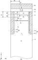
- FIG. 2 shows an example of an enlarged cross-sectional view of the mesa portion 71.
- the transistor portion 70 the XZ plane passing through the emitter region 12 is shown.
- the emitter region 12 extends from the gate trench portion 40 to the dummy trench portion 30 beyond the contact hole 54 in the trench arrangement direction. As a result, the current easily conducts from the emitter region 12 through the contact hole 54, and the electrical characteristics of the semiconductor device 100 are improved.
- the emitter region 12 of this example extends from the gate trench portion 40 to the dummy trench portion 30 in the trench arrangement direction, and terminates without reaching the dummy trench portion 30.
- the emitter region 12 may be provided extending from the gate trench portion 40 to the dummy trench portion 30 in the trench arrangement direction.
- the contact region 15 is provided on the front surface 21 of the semiconductor substrate 10 on the side wall of the dummy trench portion 30.
- the contact region 15 includes a surface region 92 and a lower region 94.
- the surface region 92 is a region of the semiconductor substrate 10 having the same depth as the emitter region 12. As an example, the depth of the surface region 92 is 0.5 ⁇ m. However, the depth of the surface region 92 may be different.
- the impurity concentration in the surface region 92 may be in the range of 5E19 / cm3 or more and 2E20 / cm3 or less.
- the lower region 94 is provided in a region deeper than the emitter region 12 in the semiconductor substrate 10.
- the lower region 94 extends beyond the lower end 13 of the emitter region 12 on the gate trench portion 40 side extending from the gate trench portion 40 to the dummy trench portion 30 toward the gate trench portion 40.
- the impurity concentration in the lower region 94 may be in the range of 1E19 / cm3 or more and 1E20 / cm3 or less.
- the width Wc is the width of the contact region 15 in the trench arrangement direction.
- the width Wc is a width measured from the center of the dummy trench portion 30 to the lower end of the emitter region 12 on the dummy trench portion 30 side. That is, the width Wc corresponds to the maximum reach position on the gate trench portion 40 side of the lower region 94 measured from the center of the dummy trench portion 30.
- the width Wc may be 1.2 ⁇ m or less, and may be 1.1 ⁇ m or less.
- the width of the surface region 92 in the trench arrangement direction may be in the range of 15% or more and 40% or less with respect to the distance between adjacent trenches.
- the width of the lower region 94 in the trench arrangement direction may be in the range of 30% or more and 70% or less with respect to the distance between adjacent trenches.
- the width of the portion where the lower region 94 overlaps the emitter region 12 in the trench arrangement direction may be in the range of 0% or more and 30% or less with respect to the distance between adjacent trenches, and more preferably 10% or more and 20. It may be in the range of% or less.
- the thickness Dc is the thickness of the contact region 15 in the depth direction of the semiconductor substrate 10.
- the thickness Dc is thicker than the depth of the lower end 13 of the emitter region 12 and less than the depth of the base region 14.
- the thickness Dc is 0.5 ⁇ m or more and 2.0 ⁇ m or less.
- the thickness of the surface region 92 may be in the range of 0.3 ⁇ m or more and 0.8 ⁇ m or less.
- the thickness of the lower region 94 may be in the range of 0.3 ⁇ m or more and 1.1 ⁇ m or less.
- the width Ws is the distance between the contact region 15 and the gate trench portion 40 in the trench arrangement direction.
- a width Ws may be provided so that a channel can be formed at the end of the gate trench 40. That is, the width Ws corresponds to the separation distance between the contact region 15 and the gate trench portion 40.
- the width Ws is 0.6 ⁇ m or more.
- the width Ws in the trench arrangement direction may be in the range of 30% or more and 70% or less with respect to the distance between adjacent trenches.
- FIG. 3 shows an example of a top view of the semiconductor device 100 having an unopened portion of the contact hole 54.
- FIG. 3 is an example of an enlarged view of the upper surface of the semiconductor device 100.
- the non-connection region 59 is a region in which the emitter electrode 52 is not electrically connected to the contact region 15 on the front surface 21.
- the non-connecting region 59 is an unopened region in which the contact hole 54 is not formed in the interlayer insulating film 38 due to poor etching of the oxide film caused by particles, foreign matter, or the like.
- the non-connection region 59 may be a region in which the contact region 15 of the front surface 21 is not formed due to the residue of resist or the like.
- the hole current that was supposed to be drawn in the non-connection region 59 flows through the contact region 15 and is pulled out through the contact hole 54 above the other neighboring contact region 15. That is, since the hole current does not flow through the base region 14 below the emitter region 12 but flows through the contact region 15 which has a lower resistance to holes than the base region 14, latch-up can be suppressed. As a result, switching failure due to process defects is suppressed. Therefore, the semiconductor device 100 having an element structure having a strong redundancy against process defects is provided.
- FIG. 4A shows an example of the simulation result of the static characteristics of the semiconductor device 100.
- the change in static characteristics with respect to the width Wc of the contact region 15 is shown.
- an example is shown in which the width of the mesa portion 71 between the dummy trench portion 30 and the gate trench portion 40 is 1.5 ⁇ m.
- the unit of each standardized value may be an appropriate unit having a dimension corresponding to each physical quantity.
- the relationship between the voltage and Vth is shown.
- FIG. 4B shows an example of the simulation result of the on-characteristics of the semiconductor device 100.
- the change of the on characteristic with respect to the width Wc of the contact region 15 is shown.
- the numerical value on the vertical axis of this example is scaled to a normalized value.
- the relationship between the maximum value di / dt_max (Normalized) of the time change and the relationship between the on-loss Eon (Normalized) of the semiconductor device 100 is shown.
- the width Wc is 1.2 ⁇ m or less, the influence of the contact region 15 on the channel formation of the base region 14 is small. Therefore, when the width Wc is in this range, the influence on all these on-characteristic values can be maintained in a small range.
- FIG. 4C shows an example of the simulation result of the off characteristic of the semiconductor device 100.
- the change of the off characteristic with respect to the width Wc of the contact region 15 is shown.
- the numerical value on the vertical axis of this example is scaled to a normalized value.
- the relationship between the maximum value di / dt_max (Normalized) of the time change and the relationship between the on-loss Off (Normalized) of the semiconductor device 100 is shown.
- the width Wc is 1.2 ⁇ m or less, the influence of the contact region 15 on the channel formation of the base region 14 is small. Therefore, when the width Wc is in this range, the influence on all these off characteristic values can be maintained in a small range.
- the semiconductor device 100 of this example does not affect the dynamic electrical characteristics due to the structure of the contact region 15. Therefore, as shown in the simulation results of FIGS. 4A to 4C, the semiconductor device 100 of this example does not significantly affect the electrical characteristics in terms of both static characteristics and dynamic characteristics.
- the semiconductor device 100 of this example improves the latch-up withstand without changing the electrical characteristics.
- FIG. 5A shows an example of a top view of the semiconductor device 100. This example differs from FIG. 1A in that the emitter region 12 is provided in contact with the dummy trench portion 30. In this example, the differences from FIG. 1A will be particularly described.
- the emitter region 12 of this example extends from the gate trench portion 40 to the dummy trench portion 30 in the trench arrangement direction.
- the emitter region 12 and the contact region 15 are provided on the front surface 21 of the semiconductor substrate 10 in alternating contact with each of the gate trench portion 40 and the dummy trench portion 30 in the trench extending direction.
- FIG. 5B is an example of a cross-sectional view taken along the line cc'in FIG. 5A.
- the cc'cross section is an XZ plane extending from the transistor portion 70 to the diode portion 80 and passing through the emitter region 12 in the transistor portion 70.
- the XZ cross section extending from the transistor portion 70 to the diode portion 80 and passing through the contact region 15 in the transistor portion 70 is the same as that in FIG. 1C.
- the surface region 92 of the contact region 15 is not provided in the cc'cross section.
- the contact region 15 of this example has a structure similar to that of the example of FIG. 1B in the lower region 94. That is, at least a part of the contact region 15 is provided below the lower end 13 in the mesa portion 71. As a result, it becomes difficult for holes below the emitter region 12 to be directly extracted through the emitter region 12, and the hole current can be extracted from the contact region 15 to suppress latch-up.
- FIG. 6A shows an example of a top view of the semiconductor device 100.
- the ratio of the number of gate trench portions 40 to the number of dummy trench portions 30 is 1: 2.
- the resistance to defects can be improved by increasing the ratio of the dummy trench portion 30.
- a gate trench portion 40 having a U-shaped structure and two dummy trench portions 30 having an I-shaped structure are arranged.
- the structures of the gate trench portion 40 and the dummy trench portion 30 are not limited to these as long as the arrangement ratio of the gate trench portion 40 and the dummy trench portion 30 can be maintained at 1: 2.
- the dummy trench portion 30 has a U-shaped structure, and the region inside the dummy trench portion may be a floating region.
- FIG. 6B is an example of a cross-sectional view taken along the line dd'in FIG. 6A.
- the dd'cross section is an XZ plane extending from the transistor portion 70 to the diode portion 80 and passing through the emitter region 12 in the transistor portion 70.
- the semiconductor device 100 of this example has a semiconductor substrate 10, an interlayer insulating film 38, an emitter electrode 52, and a collector electrode 24 in a dd'cross section.
- the emitter electrode 52 is formed above the semiconductor substrate 10 and the interlayer insulating film 38.
- the semiconductor device 100 of this example has a storage region 16 between the drift region 18 and the base region 14.
- the storage region 16 is a first conductive type region provided between the base region 14 and the drift region 18.
- the storage area 16 of this example is N + type as an example.
- the storage region 16 is provided in the transistor portion 70 and the diode portion 80. As a result, the semiconductor device 100 can avoid the mask shift of the storage region 16.
- the storage area 16 is provided in contact with the gate trench portion 40.
- the storage region 16 may or may not be in contact with the dummy trench portion 30.
- the doping concentration of the accumulation region 16 is higher than the doping concentration of the drift region 18.
- the dose amount of ion implantation in the accumulation region 16 may be 1E12 cm-2 or more and 1E13 cm- 2 or less. Further, the ion implantation dose amount of the accumulation region 16 may be 3E12 cm-2 or more and 6E12 cm- 2 or less.
- E is meant a power of 10, for example, 1E12 cm -2 refers to 1 ⁇ 10 12 cm -2.
- the contact region 15 electrically connects the contact region 15 below the emitter region 12.
- the semiconductor device 100 can suppress latch-up due to the structure of the contact region 15 regardless of the presence or absence of the storage region 16 and the arrangement ratio of the gate trench portion 40 and the dummy trench portion 30.
- FIG. 7A shows an example of a top view of the semiconductor device 100, which is a modified example.
- the semiconductor device 100 of this example includes a dummy gate trench portion 130 that does not come into contact with the emitter region 12 instead of the dummy trench portion 30.
- the dummy gate trench portion 130 is an example of a first trench portion adjacent to the gate trench portion 40.
- the dummy gate trench portion 130 is a trench portion that is set to the gate potential and does not come into contact with the emitter region 12. That is, the dummy gate trench portion 130 is a trench portion that is set to the gate potential but does not drive the transistor in the adjacent mesa portion 71, and is an example of a dummy trench portion different from the dummy trench portion 30. In order to set the dummy gate trench portion 130 to the gate potential, the dummy gate trench portion 130 extends in the Y-axis direction to the region where the gate metal layer 50 is provided. The dummy gate trench portion 130 is connected to the gate metal layer 50 via the contact hole 58 and is set to the gate potential.
- the dummy gate trench portion 130 is set to the gate potential, it is not in contact with the emitter region 12, so that a channel due to the first conductive type inversion layer is not formed on the side wall of the dummy gate trench portion 130. Since the dummy gate trench portion 130 makes it easier to attract the carrier to the mesa portion 71, the properties such as the gate capacity are different from those of the dummy gate trench portion 130. Therefore, by using the dummy gate trench portion 130 and the dummy trench portion 30 in combination, it is possible to adjust the threshold voltage, saturation current, electric field concentration, gate capacitance, etc. in the semiconductor device 100.
- the gate trench portion 40 of this example has a U-shaped structure, and the dummy gate trench portion 130 has an I-shaped structure.
- the structures of the gate trench portion 40 and the dummy gate trench portion 130 are not limited to these structures as long as the desired arrangement ratio can be achieved.
- the dummy gate trench portion 130 in the diode portion 80 has the same structure as that of FIG. 1A. That is, the dummy gate trench portion 130 is connected to the emitter electrode 52 via the contact hole 56 and is set to the emitter potential.
- FIG. 7B is an example of a cross-sectional view taken along the line ee'in FIG. 7A.
- the ee'cross section is an XZ plane extending from the transistor portion 70 to the diode portion 80 and passing through the emitter region 12 in the transistor portion 70.
- the dummy gate trench portion 130 has a second gate insulating film 132 and a second gate conductive portion 134.
- the dummy gate trench portion 130 of the semiconductor device 100 has the same configuration as the cross-sectional view in FIG. 1B, except that the dummy gate trench portion 130 has an emitter potential. That is, also in this example, the contact region 15 electrically connects the contact region 15 below the emitter region 12. Therefore, the semiconductor device 100 can suppress latch-up due to the structure of the contact region 15 regardless of the potential of the dummy gate trench portion.
- FIG. 8A shows an example of a top view of the semiconductor device 100.
- the semiconductor device 100 of this example includes a contact trench portion 60.
- the contact trench portion 60 is provided so as to extend from the front surface 21 in the depth direction of the semiconductor substrate 10.
- the contact trench portion 60 electrically connects the emitter electrode 52 and the semiconductor substrate 10.
- the contact trench portion 60 is provided so as to extend in the trench extending direction.
- the contact trench portion 60 of this example is arranged in a stripe shape along the gate trench portion 40 and the dummy trench portion 30.
- the contact trench portion 60 is formed in the transistor portion 70 above each region of the emitter region 12 and the contact region 15.
- the contact trench portion 60 is formed in the diode portion 80 above the region of the base region 14.
- the contact trench portion 60 is not provided above the well regions 17 provided at both ends in the Y-axis direction.
- the one or a plurality of contact trench portions 60 may be provided so as to extend in the trench extending direction.
- the emitter region 12 and the contact region 15 may be alternately arranged in the trench extending direction.
- the width of the emitter region 12 may be larger than the width of the contact region 15.
- the width of the emitter region 12 in the trench stretching direction may be 0.6 ⁇ m or more and 1.6 ⁇ m or less.
- FIG. 8B is an example of a cross-sectional view taken along the line ff in FIG. 8A.
- the contact trench portion 60 of this example is formed shallower than the emitter region 12.
- the contact trench portion 60 is provided so as to extend from the front surface 21 to the back surface 23 side of the semiconductor substrate 10.
- the lower end of the contact trench portion 60 of this example is shallower than the lower end of the emitter region 12.
- Emitter regions 12 are provided at both ends of the contact trench portion 60 in the trench arrangement direction.
- the contact trench portion 60 has a plug 62 and a barrier metal layer 64.
- the plug 62 is a conductive material provided inside the contact trench portion 60.
- the plug 62 may be made of the same material as the emitter electrode 52 or may be made of a different material.
- the plug 62 may contain a material such as tungsten.
- the barrier metal layer 64 is provided below the plug 62.
- the barrier metal layer 64 of this example is provided between the plug 62 and the emitter region 12.
- the barrier metal layer 64 may contain a material such as titanium nitride.
- the emitter region 12 is provided in contact with the gate trench portion 40.
- the emitter region 12 may or may not be in contact with the dummy trench portion 30.
- the emitter region 12 of this example is provided so as to extend toward the dummy trench portion 30 with respect to the contact trench portion 60 in the trench arrangement direction. That is, the lower end 13 is provided between the dummy trench portion 30 and the contact trench portion 60 in the trench arrangement direction.
- At least a part of the contact area 15 is provided below the lower end 13 in the mesa portion 71.
- the contact region 15 of this example is provided so as to extend from the dummy trench portion 30 to below the lower end 13 of the emitter region 12 in the trench arrangement direction.
- the contact region 15 may or may not extend beyond the contact trench portion 60 from the dummy trench portion 30 in the trench arrangement direction.
- the contact region 15 of this example is provided between the dummy trench portion 30 and the contact trench portion 60 in the trench arrangement direction.
- the trench bottom region 19 is a second conductive type region provided below the dummy trench portion 30 and the gate trench portion 40.
- the trench bottom region 19 of this example covers the lower ends of the dummy trench portion 30 and the gate trench portion 40.
- the doping concentration of the trench bottom region 19 may be smaller than that of the base region 14.
- the trench bottom region 19 is provided between the drift region 18a and the drift region 18b. By providing the trench bottom region 19, the avalanche withstand capacity is improved.
- the trench bottom region 19 may be omitted.
- the drift region 18a is provided between the base region 14 and the trench bottom region 19 in the mesa portion 71 and the mesa portion 81.
- the drift region 18b is provided below the trench bottom region 19.
- the doping concentrations of the drift region 18a and the drift region 18b may be the same.
- FIG. 9A shows an example of a top view of the semiconductor device 100.
- the arrangement of the emitter region 12 and the contact region 15 on the front surface 21 is different from that of the embodiment of FIG. 8A.
- the differences from the embodiment of FIG. 8A will be specifically described.
- This example differs from the embodiment of FIG. 8A in that the emitter region 12 is provided on one side of the contact trench portion 60.
- the emitter region 12 is provided in contact with the gate trench portion 40.
- the emitter region 12 is provided so as to extend from the gate trench portion 40 to the side wall of the contact trench portion 60 in the trench arrangement direction.
- the emitter region 12 does not have to be provided between the dummy trench portion 30 and the contact trench portion 60.
- FIG. 9B is an example of a cross-sectional view taken along the line gg'in FIG. 9A.
- the contact trench portion 60 of this example is formed deeper than the embodiment of FIG. 8B.
- the contact trench portion 60 is provided so as to extend from the emitter region 12 to the back surface 23 side of the semiconductor substrate 10. That is, the lower end of the contact trench portion 60 of this example is deeper than the lower end of the emitter region 12. The lower end of the contact trench portion 60 of this example is shallower than the lower end of the contact region 15.
- the emitter region 12 is provided so as to extend from the gate trench portion 40 to the side wall of the contact trench portion 60 in the trench arrangement direction. Therefore, the lower end 13 is located between the gate trench portion 40 and the contact trench portion 60 and on the side wall of the contact trench portion 60 in the trench arrangement direction.
- FIG. 10A shows an example of a top view of the semiconductor device 100.
- the semiconductor device 100 of this example differs from the embodiment of FIG. 8A in that it does not include the diode portion 80.
- FIG. 10B is an example of a cross-sectional view taken along the line h-h'in FIG. 10A.
- the contact trench portion 60 of this example is formed deeper than the embodiment of FIG. 8B.
- the contact trench portion 60 is provided so as to extend from the emitter region 12 to the back surface 23 side of the semiconductor substrate 10.
- the lower end of the contact trench portion 60 of this example is deeper than the lower end of the emitter region 12 and shallower than the lower end of the contact region 15.
- Emitter regions 12 are provided at both ends of the contact trench portion 60 in the trench arrangement direction.
- the emitter region 12 is provided so as to extend toward the dummy trench portion 30 from the contact trench portion 60 in the trench arrangement direction. That is, the lower end 13 is provided between the dummy trench portion 30 and the contact trench portion 60 in the trench arrangement direction.
- FIG. 10C is another example of the hh'cross section in FIG. 10A.
- the depth of the contact trench portion 60 is different from that of the embodiment of FIG. 10B.
- the contact trench portion 60 of this example is formed shallower than the emitter region 12. That is, the lower end of the contact trench portion 60 of this example is shallower than the lower end of the emitter region 12.
- the depth of the contact trench portion 60 is not limited to the embodiment and may be appropriately changed. Further, the emitter region 12 may be provided at both ends of the contact trench portion 60 in the trench arrangement direction, or may be provided on one side. Further, in each embodiment, the semiconductor device 100 may or may not include the trench bottom region 19.
- FIG. 11A shows an example of a top view of the semiconductor device 100.
- the semiconductor device 100 of this example includes a dummy gate trench portion 30 provided adjacent to the gate trench portion 40 and a dummy gate trench portion 130 provided adjacent to the gate trench portion 40.
- the dummy gate trench portion 130 is a trench portion that is set to the gate potential and does not come into contact with the emitter region 12.
- the dummy gate trench portion 130 of this example is connected to the extending portion 41 by the connecting portion 43.
- the emitter region 12 is provided in contact with the gate trench portion 40 and separated from the dummy gate trench portion 130 in the mesa portion 71 between the gate trench portion 40 and the dummy gate trench portion 130.
- the emitter region 12 is provided in contact with the gate trench portion 40 in the mesa portion 71 between the gate trench portion 40 and the dummy trench portion 30 and separated from the dummy trench portion 30.
- FIG. 11B is an example of a cross-sectional view taken along the line i-i'in FIG. 11A.
- the semiconductor device 100 of this example includes, but is not limited to, a contact trench portion 60 shallower than the emitter region 12 and emitter regions 12 provided at both ends of the contact trench portion 60 in the trench arrangement direction.
- the dummy gate trench portion 130 is a dummy trench like the dummy trench portion 30. Therefore, a part of the dummy gate trench portion 130 may be replaced with the dummy trench portion 30 having an emitter potential. As a result, the gate capacitance can be adjusted, so that the optimum switching speed can be realized.
- the contact region 15 is provided below the lower end 13 of the emitter region 12 on the dummy gate trench portion 130 side in the mesa portion 71 between the gate trench portion 40 and the dummy gate trench portion 130. Further, the contact region 15 is provided below the lower end 13 on the dummy trench portion 30 side of the emitter region 12 in the mesa portion 71 between the gate trench portion 40 and the dummy trench portion 30.
- FIG. 12A shows an example of a top view of the semiconductor device 100.
- the semiconductor device 100 of this example is different from the embodiment of FIG. 11A in that the first trench portion adjacent to the gate trench portion 40 is the gate trench portion 40 and has a staggered structure.
- the semiconductor device 100 has a plurality of gate trench portions 40 provided adjacent to each other.
- a plurality of gate trench portions 40 provided adjacent to each other may be connected to each other by a connecting portion 43.
- a plurality of gate trench portions 40 provided adjacent to each other are in contact with the emitter region 12 at different positions in the trench extending direction. That is, the semiconductor device 100 has a staggered structure and includes emitter regions 12 arranged in a staggered manner.
- each of the adjacent gate trench portions 40 has both a portion to be a gate trench portion and a portion to be a first trench portion. That is, in the mesa portion between the adjacent gate trench portions 40, the emitter region 12 (first emitter region) that is in contact with one gate trench portion 40 and is separated from the other gate trench portion 40, and one gate trench portion 40. It has an emitter region 12 (second emitter region) which is separated from the ground and is in contact with the other gate trench portion 40.
- the contact region 15 is provided in a region including the lower end 13 on the other gate trench portion 40 side of the first emitter region and the lower end 13 on the one gate trench portion 40 side of the second emitter region. .. Further, in the trench extending direction of the gate trench portion 40, the first emitter region and the second emitter region are alternately provided with the contact region 15 interposed therebetween.
- FIG. 12B is an example of a cross-sectional view taken along the line jj'in FIG. 12A.
- the semiconductor device 100 of this example includes, but is not limited to, a contact trench portion 60 shallower than the emitter region 12 and emitter regions 12 provided at both ends of the contact trench portion 60 in the trench arrangement direction. That is, the semiconductor device 100 may include a contact trench portion 60 deeper than the emitter region 12, or may include an emitter region 12 provided on one side of the contact trench portion 60.
- the semiconductor device 100 may or may not include the trench bottom region 19.
- FIG. 13A shows an example of a top view of the semiconductor device 100.
- the semiconductor device 100 of this example is different from the embodiment of FIG. 12A in that the dummy trench portion 30 is not provided and only the gate trench portion 40 is provided.
- the semiconductor device 100 of this example has a staggered structure in which the emitter regions 12 are alternately arranged, as in the embodiment of FIG. 12A.
- the ratio of the emitter region 12 on the front surface 21 is larger than that of the embodiment of FIG. 12A.
- the semiconductor device 100 of this example even when the ratio of the emitter region 12 on the front surface 21 is increased, a part of the emitter region 12 is separated from the gate trench portion 40, so that the semiconductor device 100 is of the semiconductor device 100. Latch-up can be suppressed.
- FIG. 13B is an example of a kk'cross section in FIG. 13A.
- the semiconductor device 100 of this example includes, but is not limited to, a contact trench portion 60 shallower than the emitter region 12 and emitter regions 12 provided at both ends of the contact trench portion 60 in the trench arrangement direction.
- the emitter region 12 of this example is provided at both ends of the gate trench portion 40 in the trench arrangement direction. In this case, by patterning the adjacent emitter regions 12 together with the gate trench portion 40 interposed therebetween, the reliability of the process can be maintained even when the mesa width becomes small.
Landscapes
- Electrodes Of Semiconductors (AREA)
- Metal-Oxide And Bipolar Metal-Oxide Semiconductor Integrated Circuits (AREA)
Abstract
ゲートトレンチ部と、ゲートトレンチ部に隣接するダミートレンチ部と、を備える半導体装置を提供する。半導体装置は半導体基板に設けられた第1導電型のドリフト領域と、ドリフト領域の上方に設けられた第2導電型のベース領域と、ベース領域の上方に設けられ、ドリフト領域よりもドーピング濃度の高い第1導電型のエミッタ領域と、ベース領域の上方に設けられ、ベース領域よりもドーピング濃度の高い第2導電型のコンタクト領域と、を備えてよい。ゲートトレンチ部とダミートレンチ部との間のメサ部において、コンタクト領域は、エミッタ領域のダミートレンチ部側の下端の下方に設けられてよい。
Description
本発明は、半導体装置に関する。
特許文献1には、「半導体装置において飽和電流等の特性を向上させる」と記載されている。
[先行技術文献]
[特許文献]
[特許文献1] 特開2018-195798号公報
[特許文献2] 国際公開第2018/052098号パンフレット
[先行技術文献]
[特許文献]
[特許文献1] 特開2018-195798号公報
[特許文献2] 国際公開第2018/052098号パンフレット
スイッチング時のラッチアップ耐量が向上した半導体装置を提供する。
本発明の第1の態様においては、ゲートトレンチ部と、ゲートトレンチ部に隣接する第1トレンチ部と、を備える半導体装置を提供する。半導体装置は半導体基板に設けられた第1導電型のドリフト領域と、ドリフト領域の上方に設けられた第2導電型のベース領域と、ベース領域の上方に設けられ、ドリフト領域よりもドーピング濃度の高い第1導電型のエミッタ領域と、ベース領域の上方に設けられ、ベース領域よりもドーピング濃度の高い第2導電型のコンタクト領域と、を備えてよい。ゲートトレンチ部と第1トレンチ部との間のメサ部において、コンタクト領域は、エミッタ領域の下端の下方に設けられてよい。
コンタクト領域は、第1トレンチ部に接してよい。
メサ部において、コンタクト領域は、ゲートトレンチ部と離間されていてよい。
コンタクト領域は、トレンチ配列方向において、ゲートトレンチ部と0.6μm以上離間されていてよい。
コンタクト領域は、第1トレンチ部の側壁において、半導体基板のおもて面に設けられてよい。
半導体装置は、半導体基板の上方に設けられた層間絶縁膜を備えてよい。エミッタ領域は、層間絶縁膜を貫通して設けられたコンタクトホールを介してエミッタ電極に電気的に接続されてよい。
エミッタ領域は、トレンチ配列方向において、ゲートトレンチ部から、コンタクトホールを越えて第1トレンチ部側へと延伸してよい。
半導体装置は、ドリフト領域とベース領域との間に、ドリフト領域よりドーピング濃度の高い第1導電型の蓄積領域を備えてよい。
半導体装置は、複数のゲートトレンチ部と、複数の第1トレンチ部とを備えてよい。複数のゲートトレンチ部の数と、複数の第1トレンチ部の数との比は1:1であってよい。
半導体装置は、複数のゲートトレンチ部と、複数の第1トレンチ部とを備えてよい。複数のゲートトレンチ部の数と、複数の第1トレンチ部の数との比は1:2であってよい。
エミッタ領域は、トレンチ配列方向において、ゲートトレンチ部からダミートレンチ部へと延伸してよい。エミッタ領域は、第1トレンチ部に到達せずに終端してよい。
エミッタ領域は、トレンチ配列方向において、ゲートトレンチ部から第1トレンチ部まで延伸してよい。
半導体装置のおもて面において、ゲートトレンチ部のトレンチ延伸方向に対して、コンタクト領域とエミッタ領域とが交互に接して設けられてよい。
第1トレンチ部は、エミッタ電位に設定されてよい。
第1トレンチ部は、ゲート電位に設定されてよい。
第1トレンチ部は、ダミートレンチであってよい。エミッタ領域は、メサ部において、ゲートトレンチ部と接し、第1トレンチ部と離間してよい。コンタクト領域は、メサ部において、エミッタ領域の第1トレンチ部側の下端の下方に設けられてよい。
第1トレンチ部は、ゲート電位に設定され、エミッタ領域と接しないダミーゲートトレンチ部を含んでよい。
第1トレンチ部は、エミッタ電位に設定されるダミートレンチ部を含んでよい。
エミッタ領域は、メサ部において、ゲートトレンチ部と接し、第1トレンチ部と離間した第1エミッタ領域を有してよい。
コンタクト領域は、メサ部において、第1エミッタ領域の第1トレンチ部側の下端の下方に設けられてよい。
コンタクト領域は、メサ部において、第1エミッタ領域の第1トレンチ部側の下端の下方に設けられてよい。
エミッタ領域は、メサ部において、第1トレンチ部と接し、ゲートトレンチ部と離間した第2エミッタ領域をさらに有してよい。
コンタクト領域は、メサ部において、第2エミッタ領域のゲートトレンチ部側の下端の下方にも設けられてよい。
コンタクト領域は、メサ部において、第2エミッタ領域のゲートトレンチ部側の下端の下方にも設けられてよい。
ゲートトレンチ部のトレンチ延伸方向において、第1エミッタ領域と第2エミッタ領域とが交互に設けられてよい。
なお、上記の発明の概要は、本発明の必要な特徴の全てを列挙したものではない。また、これらの特徴群のサブコンビネーションもまた、発明となりうる。
以下、発明の実施の形態を通じて本発明を説明するが、以下の実施形態は請求の範囲にかかる発明を限定するものではない。また、実施形態の中で説明されている特徴の組み合わせの全てが発明の解決手段に必須であるとは限らない。
本明細書においては、半導体基板の深さ方向と平行な方向における一方の側を「上」、他方の側を「下」と称する。基板、層またはその他の部材の2つの主面のうち、一方の面をおもて面、他方の面を裏面と称する。「上」、「下」、「おもて」、「裏」の方向は重力方向、または、半導体装置の実装時における基板等への取り付け方向に限定されない。
本明細書では、X軸、Y軸およびZ軸の直交座標軸を用いて技術的事項を説明する場合がある。本明細書では、半導体基板のおもて面と平行な面をXY面とし、X軸およびY軸と右手系をなす方向であって、半導体基板の深さ方向に平行な方向をZ軸とする。
各実施例においては、第1導電型をN型、第2導電型をP型とした例を示しているが、第1導電型をP型、第2導電型をN型としてもよい。この場合、各実施例における基板、層、領域等の導電型は、それぞれ逆の極性となる。
本明細書では、NまたはPを冠記した層や領域では、それぞれ電子または正孔が多数キャリアであることを意味する。また、NやPに付す+および-は、それぞれ、それらの符号が付されていない層や領域よりも高ドーピング濃度および低ドーピング濃度であることを意味する。
図1Aは、半導体装置100の上面図の一例を示す。本例の半導体装置100は、トランジスタ部70およびダイオード部80を備える半導体チップである。例えば、半導体装置100は、複数のトレンチ部を配列した、トレンチゲート型のRC-IGBT(逆導通絶縁ゲート型バイポーラトランジスタ;Reverse Conducting Insulated Gate Bipolar Transistor)である。本例において、複数のトレンチ部は、X軸方向に配列され、Y軸方向に延伸する。
トランジスタ部70は、図1Bにおいて後述される、半導体基板10の裏面側に設けられたコレクタ領域22を半導体基板10の上面に投影した領域である。コレクタ領域22は、第2導電型を有する。本例のコレクタ領域22は、一例としてP+型である。トランジスタ部70は、IGBT等のトランジスタを含む。
ダイオード部80は、図1Bにおいて後述される、半導体基板10の裏面側に設けられたカソード領域82を半導体基板10の上面に投影した領域である。カソード領域82は、第1導電型を有する。本例のカソード領域82は、一例としてN+型である。ダイオード部80は、半導体基板10の上面においてトランジスタ部70と隣接して設けられた還流ダイオード(FWD:Free Wheel Diode)等のダイオードを含む。
図1Aにおいては、半導体装置100のエッジ側であるチップ端部周辺の領域を示しており、他の領域を省略している。例えば、本例の半導体装置100におけるY軸方向の負側の領域には、エッジ終端構造部が設けられる。エッジ終端構造部は、半導体基板10の上面側の電界集中を緩和する。エッジ終端構造部は、例えばガードリング、フィールドプレート、リサーフおよびこれらを組み合わせた構造を有する。なお、本例では、便宜上、Y軸方向の負側のエッジについて説明するものの、半導体装置100の他のエッジについても同様である。
半導体基板10は、シリコン基板であってよく、炭化シリコン基板であってよく、窒化ガリウム等の窒化物半導体基板等であってもよい。本例の半導体基板10は、シリコン基板である。
本例の半導体装置100は、半導体基板10のおもて面において、ゲートトレンチ部40と、ダミートレンチ部30と、エミッタ領域12と、ベース領域14と、コンタクト領域15と、ウェル領域17とを備える。また、本例の半導体装置100は、半導体基板10のおもて面の上方に設けられたエミッタ電極52およびゲート金属層50を備える。
エミッタ電極52は、ゲートトレンチ部40、ダミートレンチ部30、エミッタ領域12、ベース領域14、コンタクト領域15およびウェル領域17の上方に設けられている。また、ゲート金属層50は、ゲートトレンチ部40およびウェル領域17の上方に設けられている。
エミッタ電極52およびゲート金属層50は、金属を含む材料で形成される。例えば、エミッタ電極52の少なくとも一部の領域は、アルミニウム、アルミニウム‐シリコン合金、またはアルミニウム‐シリコン-銅合金で形成される。ゲート金属層50の少なくとも一部の領域は、アルミニウム、アルミニウム‐シリコン合金、またはアルミニウム‐シリコン-銅合金で形成されてよい。エミッタ電極52およびゲート金属層50は、アルミニウム等で形成された領域の下層にチタンやチタン化合物等で形成されたバリアメタルを有してよい。エミッタ電極52およびゲート金属層50は、互いに分離して設けられる。
エミッタ電極52およびゲート金属層50は、層間絶縁膜38を挟んで、半導体基板10の上方に設けられる。層間絶縁膜38は、図1Aでは省略されている。層間絶縁膜38には、コンタクトホール54、コンタクトホール55およびコンタクトホール56が貫通して設けられている。
コンタクトホール55は、ゲート金属層50とトランジスタ部70のゲートトレンチ部40内のゲート導電部とを接続する。コンタクトホール55の内部には、タングステン等で形成されたプラグが形成されてもよい。
コンタクトホール56は、エミッタ電極52とダミートレンチ部30内のダミー導電部とを接続する。コンタクトホール56の内部には、タングステン等で形成されたプラグが形成されてもよい。
接続部25は、エミッタ電極52またはゲート金属層50等のおもて面側電極と、半導体基板10とを電気的に接続する。一例において、接続部25は、ゲート金属層50とゲート導電部との間に設けられる。接続部25は、エミッタ電極52とダミー導電部との間にも設けられている。接続部25は、不純物がドープされたポリシリコン等の、導電性を有する材料である。ここでは、接続部25は、N型の不純物がドープされたポリシリコン(N+)である。接続部25は、酸化膜等の絶縁膜等を介して、半導体基板10のおもて面の上方に設けられる。
ゲートトレンチ部40は、所定のトレンチ配列方向(本例ではX軸方向)に沿って所定の間隔で配列される。一例として、ゲートトレンチ部40は、1.5μmのトレンチ間隔で配列されるが、トレンチ間隔は、この間隔に限定されるものではない。本例のゲートトレンチ部40は、半導体基板10のおもて面に平行であってトレンチ配列方向と垂直なトレンチ延伸方向(本例ではY軸方向)に沿って延伸する2つの延伸部分41と、2つの延伸部分41を接続する接続部分43を有してよい。
接続部分43は、少なくとも一部が曲線状に形成されることが好ましい。ゲートトレンチ部40における2つの延伸部分41の端部を接続することで、延伸部分41の端部における電界集中を緩和できる。ゲートトレンチ部40の接続部分43において、ゲート金属層50がゲート導電部と接続されてよい。
本例のダミートレンチ部30は、エミッタ電極52と電気的に接続されて、エミッタ電位に設定されたトレンチ部である。ダミートレンチ部30は、ゲートトレンチ部40と同様に、所定のトレンチ配列方向(本例ではX軸方向)に沿って所定の間隔で配列される。一例として、ダミートレンチ部30は、1.5μmのトレンチ間隔で配列されるが、トレンチ間隔は、この間隔に限定されるものではない。特に、ダミートレンチ部30のトレンチ間隔は、ゲートトレンチ部40のトレンチ間隔と異なるように設けられてもよい。本例のダミートレンチ部30は、ゲートトレンチ部40と同様に、半導体基板10のおもて面においてU字形状を有する。即ち、ダミートレンチ部30は、トレンチ延伸方向に沿って延伸する2つの延伸部分31と、2つの延伸部分31を接続する接続部分33を有してよい。ダミートレンチ部30は、フローティング電位としてもよい。ダミートレンチ部30は、ゲートトレンチ部40に隣接する第1トレンチ部の一例である。
本例のトランジスタ部70は、接続部分43を有する2つのゲートトレンチ部40と、接続部分を有さない2つのダミートレンチ部30とを繰り返し配列させた構造を有する。即ち、ゲートトレンチ部40およびダミートレンチ部30の配列比は、予め定められた所望の配列比に設定されてよい。本例のトランジスタ部70では、ゲートトレンチ部40の数と、ダミートレンチ部30の数との比は1:1である。本例のトランジスタ部70は、接続部分43で接続された2本の延伸部分41の間にダミートレンチ部30を有する。なお、ゲートトレンチ部40の数とは、延伸部分41の数であってよい。ダミートレンチ部30の数とは、延伸部分31の数であってよい。
但し、ゲートトレンチ部40とダミートレンチ部30の比率は本例に限定されない。ゲートトレンチ部40とダミートレンチ部30の比率は、2:3であってもよく、2:4であってもよい。ゲートトレンチ部40に対して、ダミートレンチ部30の数を増大することにより、メサ部71における電界集中を緩和し、半導体装置100の電圧および電流の耐量を増大できる。また、ゲートトレンチ部40とダミートレンチ部30との比率を調整することで、半導体装置100を駆動するためのゲート容量を調整できる。ゲートトレンチ部40に対して、ダミートレンチ部30を増大させると、ゲート容量が増大し、飽和電流が低減する。また、トランジスタ部70においてダミートレンチ部30を設けず、全てゲートトレンチ部40とした所謂フルゲート構造としてもよい。なお、本明細書に開示されたゲートトレンチ部40とダミートレンチ部30の比率は、ゲートトレンチ部40とダミートレンチとの比率として読み替えられてもよい。ダミートレンチは、ダミートレンチ部30または後述するダミーゲートトレンチ部130のように、側壁にチャネルが形成されないトレンチを含む。
ウェル領域17は、後述するドリフト領域18よりも半導体基板10のおもて面側に設けられた第2導電型の領域である。ウェル領域17は、半導体装置100のエッジ側に設けられるウェル領域の一例である。ウェル領域17は、一例としてP+型である。ウェル領域17は、ゲート金属層50が設けられる側の活性領域の端部から、予め定められた範囲で形成される。ウェル領域17の拡散深さは、ゲートトレンチ部40およびダミートレンチ部30の深さよりも深くてよい。ゲートトレンチ部40およびダミートレンチ部30の、ゲート金属層50側の一部の領域は、ウェル領域17に形成される。ゲートトレンチ部40およびダミートレンチ部30のトレンチ延伸方向の端の底は、ウェル領域17に覆われてよい。
コンタクトホール54は、トランジスタ部70において、エミッタ領域12およびコンタクト領域15の各領域の上方に形成される。コンタクトホール54内には、エミッタ領域12とコンタクト領域15とが露出している。コンタクトホール54は、Y軸方向両端に設けられたウェル領域17の上方には設けられていない。このように、層間絶縁膜には、1又は複数のコンタクトホール54が形成されている。1又は複数のコンタクトホール54は、トレンチ延伸方向に延伸して設けられてよい。
メサ部71およびメサ部81は、半導体基板10のおもて面と平行な面内において、トレンチ部に隣接して設けられたメサ部である。メサ部とは、隣り合う2つのトレンチ部に挟まれた半導体基板10の部分であって、半導体基板10のおもて面から、各トレンチ部において最も深い底部の深さまでの部分であってよい。各トレンチ部の延伸部分を1つのトレンチ部としてよい。即ち、2つの延伸部分に挟まれる領域をメサ部としてよい。
メサ部71は、トランジスタ部70において、ダミートレンチ部30またはゲートトレンチ部40の少なくとも1つに隣接して設けられる。メサ部71は、半導体基板10のおもて面において、ウェル領域17と、エミッタ領域12と、ベース領域14と、コンタクト領域15とを有する。
一方、メサ部81は、ダイオード部80において、ダミートレンチ部30に隣接して設けられる。メサ部81におけるトレンチ部は、コンタクトホール56を通じて、エミッタ電極52に電気的に接続され、エミッタ電位に設定されてよい。すなわち、ダイオード部80に設けられるトレンチ部は、ダミートレンチ部30であってよい。
メサ部81は、半導体基板10のおもて面において、ウェル領域17と、ベース領域14とを有する。なお、メサ部81の上面にもエミッタ電極52が配置される。すなわち、エミッタ電極52の金属層は、ダイオード部80におけるアノード電極として機能してよい。
ベース領域14は、トランジスタ部70において、半導体基板10のおもて面側に設けられた第2導電型の領域である。ベース領域14は、一例としてP-型である。ベース領域14は、半導体基板10のおもて面21において、メサ部71のY軸方向における両端部に設けられてよい。なお、図1Aは、当該ベース領域14のY軸方向の一方の端部のみを示している。
エミッタ領域12は、図1Bにおいて後述するドリフト領域18よりもドーピング濃度の高い第1導電型の領域である。本例のエミッタ領域12は、一例としてN+型である。例えば、エミッタ領域12のドーパントは、リン(P)またはヒ素(As)等である。エミッタ領域12は、メサ部71のおもて面において、ゲートトレンチ部40と接して設けられる。エミッタ領域12は、メサ部71を挟んだ2本のトレンチ部の一方から他方まで、X軸方向に延伸して設けられてよい。エミッタ領域12は、コンタクトホール54の下方にも設けられている。
エミッタ領域12は、ダミートレンチ部30まで延伸して、ダミートレンチ部30と接してよい。ただし、エミッタ領域12は、ダミートレンチ部30に到達せずに終端し、ダミートレンチ部30に接しなくてもよい。本例のエミッタ領域12は、ダミートレンチ部30と接していない。
コンタクト領域15は、ベース領域14よりもドーピング濃度の高い第2導電型の領域である。本例のコンタクト領域15は、一例としてP+型である。コンタクト領域15のドーパントの一例は、ボロン(B)である。本例のコンタクト領域15は、メサ部71のおもて面21に設けられている。コンタクト領域15は、メサ部71を挟んだ2本のトレンチ部の一方から他方まで、X軸方向に設けられてよい。ただし、コンタクト領域15は、エミッタ領域12がゲートトレンチ部40に接する部分において、エミッタ領域12の下方でゲートトレンチ部40から離間されてよい。
コンタクト領域15は、ゲートトレンチ部40と接してもよいし、接しなくてもよい。また、コンタクト領域15は、ダミートレンチ部30と接してもよいし、接しなくてもよい。本例においては、コンタクト領域15が、ダミートレンチ部30およびゲートトレンチ部40と接する。コンタクト領域15は、コンタクトホール54の下方にも設けられている。なお、コンタクト領域15は、メサ部81にも設けられてよい。
図1Bは、図1Aにおけるa-a'断面図の一例である。a-a'断面は、トランジスタ部70からダイオード部80にわたり、トランジスタ部70において、エミッタ領域12を通過するXZ面である。本例の半導体装置100は、a-a'断面において、半導体基板10、層間絶縁膜38、エミッタ電極52およびコレクタ電極24を有する。エミッタ電極52は、半導体基板10および層間絶縁膜38の上方に形成される。
ドリフト領域18は、半導体基板10に設けられた第1導電型の領域である。本例のドリフト領域18は、一例としてN-型である。ドリフト領域18は、半導体基板10において他のドーピング領域が形成されずに残存した領域であってよい。即ち、ドリフト領域18のドーピング濃度は半導体基板10のドーピング濃度であってよい。
バッファ領域20は、ドリフト領域18の下方に設けられた第1導電型の領域である。本例のバッファ領域20は、一例としてN型である。バッファ領域20のドーピング濃度は、ドリフト領域18のドーピング濃度よりも高い。バッファ領域20は、ベース領域14の下面側から広がる空乏層が、第2導電型のコレクタ領域22および第1導電型のカソード領域82に到達することを防ぐフィールドストップ層として機能してよい。
コレクタ領域22は、トランジスタ部70において、バッファ領域20の下方に設けられる。コレクタ電極24は、半導体基板10の裏面23に形成される。コレクタ電極24は、金属等の導電材料で形成される。
ベース領域14は、メサ部71およびメサ部81において、ドリフト領域18の上方に設けられる第2導電型の領域である。ベース領域14は、ゲートトレンチ部40に接して設けられる。ベース領域14は、ダミートレンチ部30に接して設けられてよい。
エミッタ領域12は、メサ部71において、ベース領域14とおもて面21との間に設けられる。エミッタ領域12は、ゲートトレンチ部40と接して設けられる。エミッタ領域12は、ダミートレンチ部30と接してもよいし、接しなくてもよい。
1つ以上のゲートトレンチ部40および1つ以上のダミートレンチ部30は、おもて面21に設けられる。各トレンチ部は、おもて面21からドリフト領域18まで設けられる。エミッタ領域12、ベース領域14およびコンタクト領域15のうちの少なくともいずれかが設けられる領域においては、各トレンチ部はこれらの領域も貫通して、ドリフト領域18に到達する。トレンチ部がドーピング領域を貫通するとは、ドーピング領域を形成してからトレンチ部を形成する順序で製造したものに限定されない。トレンチ部を形成した後に、トレンチ部の間にドーピング領域を形成したものも、トレンチ部がドーピング領域を貫通しているものに含まれる。
ゲートトレンチ部40は、おもて面21に形成されたゲートトレンチ、ゲート絶縁膜42およびゲート導電部44を有する。ゲート絶縁膜42は、ゲートトレンチの内壁を覆って形成される。ゲート絶縁膜42は、ゲートトレンチの内壁の半導体を酸化または窒化して形成してよい。ゲート導電部44は、ゲートトレンチの内部においてゲート絶縁膜42よりも内側に形成される。ゲート絶縁膜42は、ゲート導電部44と半導体基板10とを絶縁する。ゲート導電部44は、ポリシリコン等の導電材料で形成される。ゲートトレンチ部40は、おもて面21において層間絶縁膜38により覆われる。ゲート導電部44には、IGBT等のゲート電極の電位が印加される。
ゲート導電部44は、半導体基板10の深さ方向において、ゲート絶縁膜42を挟んでメサ部71側で隣接するベース領域14と対向する領域を含む。ゲート導電部44に予め定められたゲート電圧が印加されると、ベース領域14のうちゲートトレンチに接する界面の表層に、電子の反転層によるチャネルが形成される。
ダミートレンチ部30は、ゲートトレンチ部40と同一の構造を有してよい。ダミートレンチ部30は、おもて面21側に形成されたダミートレンチ、ダミー絶縁膜32およびダミー導電部34を有する。ダミー絶縁膜32は、ダミートレンチの内壁を覆って形成される。ダミー導電部34は、ダミートレンチの内部に形成され、且つ、ダミー絶縁膜32よりも内側に形成される。ダミー絶縁膜32は、ダミー導電部34と半導体基板10とを絶縁する。ダミートレンチ部30は、おもて面21において層間絶縁膜38により覆われる。ダミー導電部34には、IGBT等のエミッタ電極の電位が印加される。ダミー導電部34は、フローティング電位としてもよい。
層間絶縁膜38は、おもて面21に設けられている。層間絶縁膜38の上方には、エミッタ電極52が設けられている。層間絶縁膜38には、エミッタ電極52と半導体基板10とを電気的に接続するための1又は複数のコンタクトホール54が設けられている。コンタクトホール55およびコンタクトホール56も同様に、層間絶縁膜38を貫通して設けられてよい。
下端13は、メサ部71におけるエミッタ領域12のダミートレンチ部30側の下端である。エミッタ領域12がダミートレンチ部30に到達する場合にあっては、下端13は、ダミートレンチ部30に接する。
コンタクト領域15の少なくとも一部は、メサ部71において下端13の下方に設けられる。すなわち、コンタクト領域15はエミッタ領域12よりも深く設けられており、かつエミッタ領域12と一部重なるように設けられる。本例のコンタクト領域15は、トレンチ配列方向において、ダミートレンチ部30からエミッタ領域12の下端13の下方まで延伸して設けられている。これにより、エミッタ領域12の下方の正孔がエミッタ領域12を通じて直接引き抜かれづらくなり、正孔電流をコンタクト領域15から引き抜かれやすくなる。これにより、エミッタ領域12からコレクタ領域22へのNPNP型の寄生サイリスタがオンしづらくなり、半導体装置100のラッチアップを抑制できる。
本例の断面において、コンタクト領域15は、メサ部71において、ゲートトレンチ部40と離間されている。これにより、コンタクト領域15が、ゲートトレンチ部40側面の反転層の形成を阻害することなく、半導体装置100が安定動作する。
本例のコンタクト領域15は、X軸方向においてダミートレンチ部30の両側にまたがって設けられている。本例のコンタクト領域15の製造プロセスでは、半導体基板10にレジストを設け、トレンチ部の設けられる領域をまたがるコンタクト領域15をイオン注入により設置できる。ダミートレンチ部30は、コンタクト領域15を設けた後に、半導体基板10にエッチングを行って設置できる。
近年では、半導体装置100の微細化等を目的として、メサ部71の間隔を短くする、所謂プロセスピッチの微細化が行われている。例えば、シリコンの半導体基板10にイオン注入により拡散領域を設ける場合、ドーパントは一定の範囲に拡散しやすい。本例のコンタクト領域15の構造により、プロセスピッチが微細化した場合であっても、エミッタ領域12の下端13の下方まで延伸し、かつ、ゲートトレンチ部40と離間されているコンタクト領域15の製造が容易となる。これにより、電気特性に大きな影響を与えず、ラッチアップ耐性の高い半導体装置100が提供できる。ただし、コンタクト領域15は、トレンチ延伸方向に接続されるように設けられればラッチアップ抑制の効果は実現でき、コンタクト領域15がダミートレンチ部30に接する形態に限定するものではない。
ダイオード部80においては、カソード領域82の上方にバッファ領域20が積層され、バッファ領域20の上方にドリフト領域18が積層される。メサ部81において、ドリフト領域18の上方にベース領域14が積層され、ベース領域14とドリフト領域18との間にPN接合が形成される。ベース領域14は、コンタクトホール54を介して、エミッタ電極52に電気的に接続される。
図1Cは、図1Aにおけるb-b'断面図の一例である。b-b'断面は、トランジスタ部70において、エミッタ領域12を通過しないXZ面である。本例において、トランジスタ部70におけるメサ部71は、ドリフト領域18の上方にベース領域14とコンタクト領域15とを有する。ダイオード部80において、メサ部81は、図1Bにおける例と同様の構造を有する。
コンタクト領域15は、ゲートトレンチ部40からダミートレンチ部30へと延伸している。コンタクト領域15の上方には、コンタクトホール54が設けられている。コンタクトホール54を介して、コンタクト領域15から正孔が引き抜かれる。
エミッタ領域12の下方に設けられるコンタクト領域15と、本例の断面におけるコンタクト領域15が同一のプロセスで設けられる場合、それらのコンタクト領域15の深さは同一の深さで設けられる。この場合、コンタクト領域15はエミッタ領域12よりも深くなる。ただし、コンタクト領域15は、エミッタ領域12の下方と他の領域とで、異なる深さで設けられてもよい。
図2は、メサ部71の拡大した断面図の一例を示す。本例では、トランジスタ部70において、エミッタ領域12を通過するXZ面を示している。
エミッタ領域12は、トレンチ配列方向において、ゲートトレンチ部40から、コンタクトホール54を越えてダミートレンチ部30へと延伸する。これにより、エミッタ領域12からコンタクトホール54を通じて電流が導通しやすくなり、半導体装置100の電気特性が良好となる。本例のエミッタ領域12は、トレンチ配列方向において、ゲートトレンチ部40からダミートレンチ部30へと延伸し、ダミートレンチ部30に到達せずに終端する。但し、エミッタ領域12は、トレンチ配列方向において、ゲートトレンチ部40からダミートレンチ部30まで延伸して設けられてもよい。
コンタクト領域15は、ダミートレンチ部30の側壁において、半導体基板10のおもて面21に設けられる。コンタクト領域15は、表面領域92および下部領域94を備える。
表面領域92は、半導体基板10において、エミッタ領域12と同一の深さを有する領域である。一例として、表面領域92の深さは、0.5μmである。ただし、表面領域92の深さは、異なる深さで設けられてもよい。エミッタ領域12がゲートトレンチ部40からダミートレンチ部30へと延伸し、ダミートレンチ部30に到達する場合には、エミッタ領域12が半導体基板10のおもて面21に露出する断面においては、表面領域92が設けられない。また表面領域92の不純物濃度は、5E19/cm3以上、2E20/cm3以下の範囲であってよい。
下部領域94は、半導体基板10において、エミッタ領域12より深い領域に設けられる。下部領域94は、ゲートトレンチ部40からダミートレンチ部30へと延伸するエミッタ領域12のゲートトレンチ部40側の下端13を越えて、ゲートトレンチ部40側へと延伸する。また下部領域94の不純物濃度は、1E19/cm3以上、1E20/cm3以下の範囲であってよい。
幅Wcは、トレンチ配列方向におけるコンタクト領域15の幅である。幅Wcは、ダミートレンチ部30の中央から、エミッタ領域12のダミートレンチ部30側の下端まで測定される幅である。すなわち、幅Wcは、ダミートレンチ部30の中央から測定される、下部領域94のゲートトレンチ部40側の最大到達位置に相当する。幅Wcは、1.2μm以下であってよく、1.1μm以下であってよい。ここで、トレンチ配列方向における表面領域92の幅は、隣り合うトレンチ間の距離に対して15%以上、40%以下の範囲であってよい。トレンチ配列方向における下部領域94の幅は、隣り合うトレンチ間の距離に対して30%以上、70%以下の範囲であってよい。また下部領域94がエミッタ領域12と重なる部分のトレンチ配列方向における幅は、隣り合うトレンチ間の距離に対して0%以上、30%以下の範囲であってよく、さらに好ましくは10%以上、20%以下の範囲であってよい。
厚みDcは、半導体基板10の深さ方向におけるコンタクト領域15の厚みである。厚みDcは、エミッタ領域12の下端13の深さより厚く、ベース領域14の深さ未満である。例えば、厚みDcは、0.5μm以上、2.0μm以下である。表面領域92の厚みは、0.3μm以上、0.8μm以下の範囲であってよい。また下部領域94の厚みは、0.3μm以上、1.1μm以下の範囲であってよい。
幅Wsは、トレンチ配列方向におけるコンタクト領域15とゲートトレンチ部40との間の距離である。ゲートトレンチ部40の端部でチャネルを形成できるように、幅Wsが設けられてよい。すなわち、幅Wsは、コンタクト領域15とゲートトレンチ部40との離間距離に相当する。一例において、幅Wsは、0.6μm以上である。またトレンチ配列方向における幅Wsは、隣り合うトレンチ間の距離に対して30%以上、70%以下の範囲であってよい。
図3は、コンタクトホール54の未開口部を備える半導体装置100の上面図の一例を示す。図3は、半導体装置100の上面の拡大図の一例である。
非接続領域59は、エミッタ電極52がおもて面21においてコンタクト領域15と電気的に接続されていない領域である。例えば、非接続領域59は、パーティクルまたは異物等に起因する酸化膜エッチング不良等により、層間絶縁膜38にコンタクトホール54が形成されていない未開口領域である。また、非接続領域59は、レジスト残り等によって、おもて面21のコンタクト領域15が形成されなかった領域であってよい。
本例では、非接続領域59において引き抜かれるはずであった正孔電流は、コンタクト領域15を流れて他の近隣のコンタクト領域15上方のコンタクトホール54を介して引き抜かれる。即ち、正孔電流がエミッタ領域12の下方のベース領域14を流れずに、ベース領域14よりも正孔に対して低抵抗であるコンタクト領域15を流れるので、ラッチアップを抑制できる。これにより、プロセス欠陥起因のスイッチング破壊が抑制される。従って、プロセス欠陥に強い冗長性のある素子構造を有する半導体装置100が提供される。
図4Aは、半導体装置100の静特性のシミュレーション結果の一例を示す。本例では、コンタクト領域15の幅Wcに対する静特性の変化を示す。本例では、ダミートレンチ部30とゲートトレンチ部40との間におけるメサ部71の幅が、1.5μmの場合の例が示される。なお、シミュレーション結果における定性的性質を示すべく、本例の縦軸の数値は、コンタクト領域の幅Wc=0に対応する初期値が1に規格化された(Normalized)値にスケーリングされている。各規格化値が有する単位は、各物理量に応じた次元を有する適切な単位であってよい。
幅Wcに対して、半導体装置100が駆動した場合のコレクタ-エミッタ間の飽和電圧Vceの関係と、半導体装置100が駆動した場合のコレクタ-エミッタ間の飽和電流の関係と、半導体装置100の閾値電圧Vthの関係とが示される。幅Wcが1.2μm以下の場合、コンタクト領域15がベース領域14のチャネル形成に与える影響は小さい。従って、幅Wcがこの範囲の場合、これら全ての静特性値に対する影響を小さい範囲に維持できる。
図4Bは、半導体装置100のオン特性のシミュレーション結果の一例を示す。本例では、コンタクト領域15の幅Wcに対するオン特性の変化を示す。なお、本例の縦軸の数値に関しては、規格化された(Normalized)値にスケーリングされている。
Wcに対して、半導体装置100を駆動する場合のコレクタ-エミッタ間の電圧Vceの時間変化の最大値dV/dt_max(Normalized)の関係と、半導体装置100が駆動する場合のコレクタ-エミッタ間の電流の時間変化の最大値di/dt_max(Normalized)の関係と、半導体装置100のオン損失Eon(Normalized)の関係とが示される。幅Wcが1.2μm以下の場合、コンタクト領域15がベース領域14のチャネル形成に与える影響は小さい。従って、幅Wcがこの範囲の場合、これら全てのオン特性値に対する影響を小さい範囲に維持できる。
図4Cは、半導体装置100のオフ特性のシミュレーション結果の一例を示す。本例では、コンタクト領域15の幅Wcに対するオフ特性の変化を示す。なお、本例の縦軸の数値に関しては、規格化された(Normalized)値にスケーリングされている。
Wcに対して、半導体装置100を駆動する場合のコレクタ-エミッタ間の電圧Vceの時間変化の最大値dV/dt_max(Normalized)の関係と、半導体装置100が駆動する場合のコレクタ-エミッタ間の電流の時間変化の最大値di/dt_max(Normalized)の関係と、半導体装置100のオン損失Eoff(Normalized)の関係とが示される。幅Wcが1.2μm以下の場合、コンタクト領域15がベース領域14のチャネル形成に与える影響は小さい。従って、幅Wcがこの範囲の場合、これら全てのオフ特性値に対する影響を小さい範囲に維持できる。
図4Bおよび図4Cのシミュレーション結果に示される通り、本例の半導体装置100は、コンタクト領域15の構造により、動的な電気特性にも影響を与えない。従って、図4Aから図4Cのシミュレーション結果に示される通り、本例の半導体装置100は、静特性および動特性の両方において電気特性に大きな影響を与えない。本例の半導体装置100は、電気特性に変動を与えずに、ラッチアップ耐量を向上させる。
図5Aは、半導体装置100の上面図の一例を示す。本例では、エミッタ領域12がダミートレンチ部30に接して設けられている点で図1Aと相違する。本例では、図1Aと相違する点について特に説明する。
本例のエミッタ領域12は、トレンチ配列方向において、ゲートトレンチ部40からダミートレンチ部30まで延伸する。エミッタ領域12およびコンタクト領域15は、半導体基板10のおもて面21において、トレンチ延伸方向に対して、ゲートトレンチ部40およびダミートレンチ部30のそれぞれに交互に接して設けられている。
図5Bは、図5Aにおけるc-c'断面図の一例である。c-c'断面は、トランジスタ部70からダイオード部80にわたり、トランジスタ部70においてエミッタ領域12を通過するXZ面である。なお、トランジスタ部70からダイオード部80にわたり、トランジスタ部70においてコンタクト領域15を通過するXZ断面は、図1Cと同じとなる。
本例では、c-c'断面において、コンタクト領域15の表面領域92が設けられない。本例のコンタクト領域15は、下部領域94において、図1Bの例と同様の構造を有する。すなわち、コンタクト領域15の少なくとも一部は、メサ部71において下端13の下方に設けられる。これにより、エミッタ領域12の下方の正孔がエミッタ領域12を通じて直接引き抜かれづらくなり、正孔電流をコンタクト領域15から引き抜いてラッチアップを抑制できる。
図6Aは、半導体装置100の上面図の一例を示す。本例では、ゲートトレンチ部40の数とダミートレンチ部30の数との比が1:2である。本例の半導体装置100は、ダミートレンチ部30の比率を高めることにより、欠陥に対する耐量を向上させることができる。
本例では、半導体基板10のおもて面のトランジスタ部70において、U型の構造のゲートトレンチ部40と、二本のI型の構造のダミートレンチ部30が配列される。ただし、ゲートトレンチ部40およびダミートレンチ部30の配列比を1:2に保持できる限り、ゲートトレンチ部40およびダミートレンチ部30の構造は、これらに限定されない。一例として、ダミートレンチ部30は、U型の構造を有し、ダミートレンチ部内の領域がフローティング領域になってもよい。
図6Bは、図6Aにおけるd-d'断面図の一例である。d-d'断面は、トランジスタ部70からダイオード部80にわたり、トランジスタ部70において、エミッタ領域12を通過するXZ面である。
本例の半導体装置100は、d-d'断面において、半導体基板10、層間絶縁膜38、エミッタ電極52およびコレクタ電極24を有する。エミッタ電極52は、半導体基板10および層間絶縁膜38の上方に形成される。また、本例の半導体装置100は、ドリフト領域18とベース領域14との間に蓄積領域16を有する。
本例の半導体装置100は、d-d'断面において、半導体基板10、層間絶縁膜38、エミッタ電極52およびコレクタ電極24を有する。エミッタ電極52は、半導体基板10および層間絶縁膜38の上方に形成される。また、本例の半導体装置100は、ドリフト領域18とベース領域14との間に蓄積領域16を有する。
蓄積領域16は、ベース領域14とドリフト領域18との間に設けられる第1導電型の領域である。本例の蓄積領域16は、一例としてN+型である。蓄積領域16は、トランジスタ部70およびダイオード部80に設けられる。これにより、半導体装置100は、蓄積領域16のマスクずれを回避できる。
また、蓄積領域16は、ゲートトレンチ部40に接して設けられる。蓄積領域16は、ダミートレンチ部30に接してもよいし、接しなくてもよい。蓄積領域16のドーピング濃度は、ドリフト領域18のドーピング濃度よりも高い。蓄積領域16のイオン注入のドーズ量は、1E12cm-2以上、1E13cm-2以下であってよい。また、蓄積領域16のイオン注入ドーズ量は、3E12cm-2以上、6E12cm-2以下であってもよい。蓄積領域16を設けることで、キャリア注入促進効果(Injection Enhancement effect)を高めて、トランジスタ部70のオン電圧を低減できる。なお、Eは10のべき乗を意味し、例えば1E12cm-2は1×1012cm-2を意味する。
本例でも、コンタクト領域15がエミッタ領域12の下方において、コンタクト領域15を電気的に接続する。半導体装置100は、蓄積領域16の有無と、ゲートトレンチ部40およびダミートレンチ部30の配列比とに関わらず、コンタクト領域15の構造によりラッチアップを抑制できる。
図7Aは、変形例である半導体装置100の上面図の一例を示す。本例では、図1Aと相違する点について特に説明する。本例の半導体装置100は、ダミートレンチ部30に替えて、エミッタ領域12と接しないダミーゲートトレンチ部130を備える。ダミーゲートトレンチ部130は、ゲートトレンチ部40に隣接する第1トレンチ部の一例である。
ダミーゲートトレンチ部130は、ゲート電位に設定され、エミッタ領域12と接触しないトレンチ部である。すなわち、ダミーゲートトレンチ部130は、ゲート電位に設定されるものの、隣接するメサ部71においてトランジスタを駆動しないトレンチ部であり、ダミートレンチ部30とは別のダミートレンチ部の例である。ダミーゲートトレンチ部130をゲート電位に設定すべく、ダミーゲートトレンチ部130は、ゲート金属層50の設けられる領域までY軸方向に延伸する。ダミーゲートトレンチ部130は、コンタクトホール58を介してゲート金属層50に接続され、ゲート電位に設定される。
ダミーゲートトレンチ部130は、ゲート電位に設定されているものの、エミッタ領域12と接触していないので、ダミーゲートトレンチ部130の側壁においては、第1導電型の反転層によるチャネルが形成されない。ダミーゲートトレンチ部130は、キャリアをメサ部71に引き寄せ易くするので、ダミーゲートトレンチ部130とゲート容量等の性質が異なる。従って、ダミーゲートトレンチ部130およびダミートレンチ部30を組み合わせて使用することにより、半導体装置100における閾値電圧、飽和電流、電界集中およびゲート容量等の調整が実行できる。
半導体基板10のおもて面において、本例のゲートトレンチ部40はU型の構造を有し、ダミーゲートトレンチ部130はI型の構造を有している。ただし、ゲートトレンチ部40およびダミーゲートトレンチ部130の構造は所望の配列比が達成できる限り、これらの構造に限定されない。
本例において、ダイオード部80におけるダミーゲートトレンチ部130は、図1Aの構造と同様である。すなわち、ダミーゲートトレンチ部130は、コンタクトホール56を介してエミッタ電極52に接続され、エミッタ電位に設定される。
図7Bは、図7Aにおけるe-e'断面図の一例である。e-e'断面は、トランジスタ部70からダイオード部80にわたり、トランジスタ部70において、エミッタ領域12を通過するXZ面である。ダミーゲートトレンチ部130は、第2ゲート絶縁膜132および第2ゲート導電部134を有する。
本例では、半導体装置100の有するダミーゲートトレンチ部130がエミッタ電位を有することを除いて、図1Bにおける断面図と同様の構成を有する。すなわち、本例でも、コンタクト領域15がエミッタ領域12の下方において、コンタクト領域15を電気的に接続する。従って、半導体装置100は、ダミーゲートトレンチ部の有する電位に関わらず、コンタクト領域15の構造によりラッチアップを抑制できる。
図8Aは、半導体装置100の上面図の一例を示す。本例の半導体装置100は、コンタクトトレンチ部60を備える。
コンタクトトレンチ部60は、おもて面21から半導体基板10の深さ方向に延伸して設けられる。コンタクトトレンチ部60は、エミッタ電極52と半導体基板10とを電気的に接続する。コンタクトトレンチ部60は、トレンチ延伸方向に延伸して設けられている。本例のコンタクトトレンチ部60は、ゲートトレンチ部40およびダミートレンチ部30に沿ってストライプ状に配置されている。
コンタクトトレンチ部60は、トランジスタ部70において、エミッタ領域12およびコンタクト領域15の各領域の上方に形成される。コンタクトトレンチ部60は、ダイオード部80において、ベース領域14の領域の上方に形成される。コンタクトトレンチ部60は、Y軸方向両端に設けられたウェル領域17の上方には設けられていない。1又は複数のコンタクトトレンチ部60は、トレンチ延伸方向に延伸して設けられてよい。
ゲートトレンチ部40とコンタクトトレンチ部60との間のメサ部71において、エミッタ領域12およびコンタクト領域15は、トレンチ延伸方向に交互に配置されてよい。トレンチ延伸方向において、エミッタ領域12の幅は、コンタクト領域15の幅よりも大きくてよい。トレンチ延伸方向におけるエミッタ領域12の幅は、0.6μm以上、1.6μm以下であってよい。エミッタ領域12とコンタクト領域15の比率を適切に制御することにより、ラッチアップを抑制しやすくなる。
図8Bは、図8Aにおけるf-f'断面図の一例である。本例のコンタクトトレンチ部60は、エミッタ領域12よりも浅く形成されている。
コンタクトトレンチ部60は、おもて面21よりも半導体基板10の裏面23側に延伸して設けられる。本例のコンタクトトレンチ部60の下端は、エミッタ領域12の下端よりも浅い。トレンチ配列方向におけるコンタクトトレンチ部60の両端には、エミッタ領域12が設けられている。コンタクトトレンチ部60は、プラグ62およびバリアメタル層64を有する。
プラグ62は、コンタクトトレンチ部60の内部に設けられる導電性の材料である。プラグ62は、エミッタ電極52と同一の材料であっても、異なる材料であってもよい。プラグ62は、タングステン等の材料を含んでよい。
バリアメタル層64は、プラグ62の下方に設けられる。本例のバリアメタル層64は、プラグ62とエミッタ領域12との間に設けられる。バリアメタル層64は、窒化チタンなどの材料を含んでよい。
エミッタ領域12は、ゲートトレンチ部40と接して設けられる。エミッタ領域12は、ダミートレンチ部30と接してもよいし、接しなくてもよい。本例のエミッタ領域12は、トレンチ配列方向において、コンタクトトレンチ部60よりもダミートレンチ部30側に延伸して設けられる。即ち、下端13は、トレンチ配列方向において、ダミートレンチ部30とコンタクトトレンチ部60との間に設けられる。
コンタクト領域15の少なくとも一部は、メサ部71において下端13の下方に設けられる。本例のコンタクト領域15は、トレンチ配列方向において、ダミートレンチ部30からエミッタ領域12の下端13の下方まで延伸して設けられている。コンタクト領域15は、トレンチ配列方向において、ダミートレンチ部30からコンタクトトレンチ部60を超えて延伸してもよいし、コンタクトトレンチ部60を超えなくてもよい。本例のコンタクト領域15は、トレンチ配列方向において、ダミートレンチ部30とコンタクトトレンチ部60との間に設けられる。
トレンチボトム領域19は、ダミートレンチ部30およびゲートトレンチ部40の下方に設けられた第2導電型の領域である。本例のトレンチボトム領域19は、ダミートレンチ部30およびゲートトレンチ部40の下端を覆っている。トレンチボトム領域19のドーピング濃度は、ベース領域14よりも小さくてよい。トレンチボトム領域19は、ドリフト領域18aとドリフト領域18bとの間に設けられる。トレンチボトム領域19を設けることにより、アバランシェ耐量が向上する。なお、半導体装置100がトレンチボトム領域19を備える実施形態を説明する場合があるが、トレンチボトム領域19は省略されてもよい。
ドリフト領域18aは、メサ部71およびメサ部81において、ベース領域14とトレンチボトム領域19との間に設けられる。ドリフト領域18bは、トレンチボトム領域19の下方に設けられる。ドリフト領域18aおよびドリフト領域18bのドーピング濃度は、同一であってよい。
図9Aは、半導体装置100の上面図の一例を示す。本例の半導体装置100は、おもて面21におけるエミッタ領域12とコンタクト領域15の配置が、図8Aの実施形態と相違する。本例では、図8Aの実施形態と相違する点について特に説明する。本例では、コンタクトトレンチ部60の片側にエミッタ領域12が設けられている点で図8Aの実施形態と相違する。
エミッタ領域12は、ゲートトレンチ部40と接して設けられる。エミッタ領域12は、トレンチ配列方向において、ゲートトレンチ部40からコンタクトトレンチ部60の側壁まで延伸して設けられる。エミッタ領域12は、ダミートレンチ部30とコンタクトトレンチ部60との間に設けられなくてもよい。
図9Bは、図9Aにおけるg-g'断面図の一例である。本例のコンタクトトレンチ部60は、図8Bの実施形態よりも深く形成されている。
コンタクトトレンチ部60は、エミッタ領域12よりも半導体基板10の裏面23側に延伸して設けられる。即ち、本例のコンタクトトレンチ部60の下端は、エミッタ領域12の下端よりも深い。本例のコンタクトトレンチ部60の下端は、コンタクト領域15の下端よりも浅い。
エミッタ領域12は、トレンチ配列方向において、ゲートトレンチ部40からコンタクトトレンチ部60の側壁まで延伸して設けられる。よって、下端13は、トレンチ配列方向において、ゲートトレンチ部40とコンタクトトレンチ部60との間であって、コンタクトトレンチ部60の側壁に位置する。
図10Aは、半導体装置100の上面図の一例を示す。本例の半導体装置100は、ダイオード部80を備えていない点で図8Aの実施形態と相違する。
図10Bは、図10Aにおけるh-h'断面図の一例である。本例のコンタクトトレンチ部60は、図8Bの実施形態よりも深く形成されている。
コンタクトトレンチ部60は、エミッタ領域12よりも半導体基板10の裏面23側に延伸して設けられる。本例のコンタクトトレンチ部60の下端は、エミッタ領域12の下端よりも深く、コンタクト領域15の下端よりも浅い。トレンチ配列方向におけるコンタクトトレンチ部60の両端には、エミッタ領域12が設けられている。
エミッタ領域12は、トレンチ配列方向において、コンタクトトレンチ部60よりもダミートレンチ部30側に延伸して設けられる。即ち、下端13は、トレンチ配列方向において、ダミートレンチ部30とコンタクトトレンチ部60との間に設けられる。
図10Cは、図10Aにおけるh-h'断面図の他の例である。本例では、コンタクトトレンチ部60の深さが図10Bの実施形態と相違する。本例のコンタクトトレンチ部60は、エミッタ領域12よりも浅く形成されている。即ち、本例のコンタクトトレンチ部60の下端は、エミッタ領域12の下端よりも浅い。
以上の通り、コンタクトトレンチ部60の深さは、実施形態に限定されず、適宜変更されてよい。また、エミッタ領域12は、トレンチ配列方向におけるコンタクトトレンチ部60の両端に設けられてもよいし、片側に設けられてもよい。また、各実施形態において、半導体装置100は、トレンチボトム領域19を備えてもよいし、備えなくともよい。
図11Aは、半導体装置100の上面図の一例を示す。本例の半導体装置100は、ゲートトレンチ部40と隣接して設けられたダミートレンチ部30とともに、ゲートトレンチ部40と隣接して設けられたダミーゲートトレンチ部130を備える。
ダミーゲートトレンチ部130は、ゲート電位に設定され、エミッタ領域12と接触しないトレンチ部である。本例のダミーゲートトレンチ部130は、接続部分43によって延伸部分41と連結されている。
エミッタ領域12は、ゲートトレンチ部40とダミーゲートトレンチ部130との間のメサ部71において、ゲートトレンチ部40と接し、ダミーゲートトレンチ部130と離間して設けられている。
また、エミッタ領域12は、ゲートトレンチ部40とダミートレンチ部30との間のメサ部71において、ゲートトレンチ部40と接し、ダミートレンチ部30と離間して設けられている。
図11Bは、図11Aにおけるi-i'断面図の一例である。本例の半導体装置100は、エミッタ領域12よりも浅いコンタクトトレンチ部60と、トレンチ配列方向においてコンタクトトレンチ部60の両端に設けられたエミッタ領域12とを備えるが、これに限定されない。ダミーゲートトレンチ部130はダミートレンチ部30と同じくダミートレンチである。このため、ダミーゲートトレンチ部130の一部を、エミッタ電位のダミートレンチ部30に置き換えてもよい。これによりゲート容量を調節できるので、最適なスイッチング速度を実現できる。
コンタクト領域15は、ゲートトレンチ部40とダミーゲートトレンチ部130との間のメサ部71において、エミッタ領域12のダミーゲートトレンチ部130側の下端13の下方に設けられている。また、コンタクト領域15は、ゲートトレンチ部40とダミートレンチ部30との間のメサ部71において、エミッタ領域12のダミートレンチ部30側の下端13の下方に設けられている。
図12Aは、半導体装置100の上面図の一例を示す。本例の半導体装置100は、ゲートトレンチ部40に隣接する第1トレンチ部がゲートトレンチ部40の場合であり、千鳥構造を備える点で図11Aの実施形態と相違する。半導体装置100は、隣接して設けられた複数のゲートトレンチ部40を有する。隣接して設けられた複数のゲートトレンチ部40は、接続部分43で互いに接続されてよい。
隣接して設けられた複数のゲートトレンチ部40は、トレンチ延伸方向における異なる位置で、エミッタ領域12と接触している。即ち、半導体装置100は、千鳥構造を有し、互い違いに配列されたエミッタ領域12を備える。この場合、隣り合うゲートトレンチ部40の各々が、ゲートトレンチ部となる部分と第1トレンチ部となる部分とを共に有する。つまり、隣り合うゲートトレンチ部40の間のメサ部において、片方のゲートトレンチ部40と接し、他方のゲートトレンチ部40と離間したエミッタ領域12(第1エミッタ領域)と、片方のゲートトレンチ部40と離間し、他方のゲートトレンチ部40と接するエミッタ領域12(第2エミッタ領域)と、を有する。そしてコンタクト領域15は、第1エミッタ領域の他方のゲートトレンチ部40側の下端13の下方と、第2エミッタ領域の片方のゲートトレンチ部40側の下端13の下方と、を含む領域に設けられる。またゲートトレンチ部40のトレンチ延伸方向において、第1エミッタ領域と第2エミッタ領域とは、コンタクト領域15を挟んで交互に設けられる。
図12Bは、図12Aにおけるj-j'断面図の一例である。本例の半導体装置100は、エミッタ領域12よりも浅いコンタクトトレンチ部60と、トレンチ配列方向においてコンタクトトレンチ部60の両端に設けられたエミッタ領域12とを備えるが、これに限定されない。即ち、半導体装置100は、エミッタ領域12よりも深いコンタクトトレンチ部60を備えてもよいし、コンタクトトレンチ部60の片側に設けられたエミッタ領域12を備えてもよい。半導体装置100は、トレンチボトム領域19を備えていてもよいし、備えていなくてもよい。
図13Aは、半導体装置100の上面図の一例を示す。本例の半導体装置100においては、ダミートレンチ部30が設けられず、ゲートトレンチ部40のみが設けられている点で図12Aの実施形態と相違する。本例の半導体装置100は、図12Aの実施形態と同様に、エミッタ領域12が互い違いに配列された千鳥構造を有する。本例の半導体装置100は、図12Aの実施形態よりも、おもて面21におけるエミッタ領域12の比率が大きい。本例の半導体装置100は、おもて面21におけるエミッタ領域12の比率を大きくした場合であっても、エミッタ領域12の一部がゲートトレンチ部40と離間されているため、半導体装置100のラッチアップを抑制できる。
図13Bは、図13Aにおけるk-k'断面図の一例である。本例の半導体装置100は、エミッタ領域12よりも浅いコンタクトトレンチ部60と、トレンチ配列方向においてコンタクトトレンチ部60の両端に設けられたエミッタ領域12とを備えるが、これに限定されない。本例のエミッタ領域12は、トレンチ配列方向において、ゲートトレンチ部40を挟んで両端に設けられる。この場合、ゲートトレンチ部40を挟んで隣接するエミッタ領域12をまとめてパターニングすることにより、メサ幅が小さくなった場合においてもプロセスの信頼性を維持することができる。
以上、本発明を実施の形態を用いて説明したが、本発明の技術的範囲は上記実施の形態に記載の範囲には限定されない。上記実施の形態に、多様な変更または改良を加えることが可能であることが当業者に明らかである。その様な変更または改良を加えた形態も本発明の技術的範囲に含まれ得ることが、請求の範囲の記載から明らかである。例えば、本例ではRC-IGBTを例にとり説明したが、IGBTやMOSFETにも適用可能である。
請求の範囲、明細書、および図面中において示した装置、システム、プログラム、および方法における動作、手順、ステップ、および段階等の各処理の実行順序は、特段「より前に」、「先立って」等と明示しておらず、また、前の処理の出力を後の処理で用いるのでない限り、任意の順序で実現しうることに留意すべきである。請求の範囲、明細書、および図面中の動作フローに関して、便宜上「まず、」、「次に、」等を用いて説明したとしても、この順で実施することが必須であることを意味するものではない。
10・・・半導体基板、12・・・エミッタ領域、13・・・下端、14・・・ベース領域、15・・・コンタクト領域、16・・・蓄積領域、17・・・ウェル領域、18・・・ドリフト領域、19・・・トレンチボトム領域、20・・・バッファ領域、21・・・おもて面、22・・・コレクタ領域、23・・・裏面、24・・・コレクタ電極、25・・・接続部、30・・・ダミートレンチ部、31・・・延伸部分、32・・・ダミー絶縁膜、33・・・接続部分、34・・・ダミー導電部、38・・・層間絶縁膜、40・・・ゲートトレンチ部、41・・・延伸部分、42・・・ゲート絶縁膜、43・・・接続部分、44・・・ゲート導電部、50・・・ゲート金属層、52・・・エミッタ電極、54・・・コンタクトホール、55・・・コンタクトホール、56・・・コンタクトホール、58・・・コンタクトホール、59・・・非接続領域、60・・・コンタクトトレンチ部、62・・・プラグ、64・・・バリアメタル層、70・・・トランジスタ部、71・・・メサ部、80・・・ダイオード部、81・・・メサ部、82・・・カソード領域、92・・・表面領域、94・・・下部領域、100・・・半導体装置、130・・・ダミーゲートトレンチ部、132・・・第2ゲート絶縁膜、134・・・第2ゲート導電部
Claims (21)
- ゲートトレンチ部と、前記ゲートトレンチ部に隣接する第1トレンチ部と、を備える半導体装置であって、
半導体基板に設けられた第1導電型のドリフト領域と、
前記ドリフト領域の上方に設けられた第2導電型のベース領域と、
前記ベース領域の上方に設けられ、前記ドリフト領域よりもドーピング濃度の高い第1導電型のエミッタ領域と、
前記ベース領域の上方に設けられ、前記ベース領域よりもドーピング濃度の高い第2導電型のコンタクト領域と、
を備え、
前記ゲートトレンチ部と前記第1トレンチ部との間のメサ部において、前記コンタクト領域は、前記エミッタ領域の下端の下方に設けられる、
半導体装置。 - 前記コンタクト領域は、前記第1トレンチ部に接する
請求項1に記載の半導体装置。 - 前記メサ部において、前記コンタクト領域は、前記ゲートトレンチ部と離間されている、
請求項1または2に記載の半導体装置。 - 前記コンタクト領域は、トレンチ配列方向において、前記ゲートトレンチ部と0.6μm以上離間されている、
請求項3に記載の半導体装置。 - 前記コンタクト領域は、前記第1トレンチ部の側壁において、前記半導体基板のおもて面に設けられる
請求項1から4のいずれか一項に記載の半導体装置。 - 前記半導体基板の上方に設けられた層間絶縁膜を備え、
前記エミッタ領域は、前記層間絶縁膜を貫通して設けられたコンタクトホールを介してエミッタ電極に電気的に接続される、
請求項1から5のいずれか一項に記載の半導体装置。 - 前記エミッタ領域は、トレンチ配列方向において、前記ゲートトレンチ部から、前記コンタクトホールを越えて前記第1トレンチ部側へと延伸する、
請求項6に記載の半導体装置。 - 前記ドリフト領域と前記ベース領域との間に、前記ドリフト領域よりドーピング濃度の高い第1導電型の蓄積領域を備える、
請求項1から7のいずれか一項に記載の半導体装置。 - 複数の前記ゲートトレンチ部と、複数の前記第1トレンチ部とを備え、
複数の前記ゲートトレンチ部の数と、複数の前記第1トレンチ部の数との比は1:1である、
請求項1から8のいずれか一項に記載の半導体装置。 - 複数の前記ゲートトレンチ部と、複数の前記第1トレンチ部とを備え、
複数の前記ゲートトレンチ部の数と、複数の前記第1トレンチ部の数との比は1:2である、
請求項1から9のいずれか一項に記載の半導体装置。 - 前記エミッタ領域は、トレンチ配列方向において、前記ゲートトレンチ部から前記第1トレンチ部へと延伸し、前記第1トレンチ部に到達せずに終端する、
請求項1から10のいずれか一項に記載の半導体装置。 - 前記エミッタ領域は、トレンチ配列方向において、前記ゲートトレンチ部から前記第1トレンチ部まで延伸する、
請求項1から11のいずれか一項に記載の半導体装置。 - 前記半導体装置のおもて面において、前記ゲートトレンチ部のトレンチ延伸方向に対して、前記コンタクト領域と前記エミッタ領域とが交互に接して設けられる、
請求項12に記載の半導体装置。 - 前記第1トレンチ部は、エミッタ電位に設定される、
請求項1から13のいずれか一項に記載の半導体装置。 - 前記第1トレンチ部は、ゲート電位に設定される、
請求項1から11のいずれか一項に記載の半導体装置。 - 前記第1トレンチ部は、ダミートレンチであり、
前記エミッタ領域は、前記メサ部において、前記ゲートトレンチ部と接し、前記第1トレンチ部と離間しており、
前記コンタクト領域は、前記メサ部において、前記エミッタ領域の前記第1トレンチ部側の下端の下方に設けられる、
請求項1から15のいずれか一項に記載の半導体装置。 - 前記第1トレンチ部は、ゲート電位に設定され、前記エミッタ領域と接しないダミーゲートトレンチ部を含む、
請求項16に記載の半導体装置。 - 前記第1トレンチ部は、エミッタ電位に設定されるダミートレンチ部を含む、
請求項16に記載の半導体装置。 - 前記エミッタ領域は、前記メサ部において、前記ゲートトレンチ部と接し、前記第1トレンチ部と離間した第1エミッタ領域を有し、
前記コンタクト領域は、前記メサ部において、前記第1エミッタ領域の前記第1トレンチ部側の下端の下方に設けられる
請求項15に記載の半導体装置。 - 前記エミッタ領域は、前記メサ部において、前記第1トレンチ部と接し、前記ゲートトレンチ部と離間した第2エミッタ領域をさらに有し、
前記コンタクト領域は、前記メサ部において、前記第2エミッタ領域の前記ゲートトレンチ部側の下端の下方にも設けられる
請求項19に記載の半導体装置。 - 前記ゲートトレンチ部のトレンチ延伸方向において、前記第1エミッタ領域と前記第2エミッタ領域とが交互に設けられる
請求項20に記載の半導体装置。
Priority Applications (6)
| Application Number | Priority Date | Filing Date | Title |
|---|---|---|---|
| DE112021000202.3T DE112021000202T5 (de) | 2020-07-03 | 2021-04-01 | Halbleitervorrichtung |
| JP2022533692A JP7327672B2 (ja) | 2020-07-03 | 2021-04-01 | 半導体装置 |
| CN202180007468.1A CN114846622A (zh) | 2020-07-03 | 2021-04-01 | 半导体装置 |
| US17/847,167 US20220328669A1 (en) | 2020-07-03 | 2022-06-23 | Semiconductor device |
| JP2023123888A JP7726248B2 (ja) | 2020-07-03 | 2023-07-28 | 半導体装置 |
| JP2025127679A JP2025160397A (ja) | 2020-07-03 | 2025-07-30 | 半導体装置 |
Applications Claiming Priority (2)
| Application Number | Priority Date | Filing Date | Title |
|---|---|---|---|
| JP2020-115759 | 2020-07-03 | ||
| JP2020115759 | 2020-07-03 |
Related Child Applications (1)
| Application Number | Title | Priority Date | Filing Date |
|---|---|---|---|
| US17/847,167 Continuation US20220328669A1 (en) | 2020-07-03 | 2022-06-23 | Semiconductor device |
Publications (1)
| Publication Number | Publication Date |
|---|---|
| WO2022004084A1 true WO2022004084A1 (ja) | 2022-01-06 |
Family
ID=79315725
Family Applications (1)
| Application Number | Title | Priority Date | Filing Date |
|---|---|---|---|
| PCT/JP2021/014138 Ceased WO2022004084A1 (ja) | 2020-07-03 | 2021-04-01 | 半導体装置 |
Country Status (5)
| Country | Link |
|---|---|
| US (1) | US20220328669A1 (ja) |
| JP (3) | JP7327672B2 (ja) |
| CN (1) | CN114846622A (ja) |
| DE (1) | DE112021000202T5 (ja) |
| WO (1) | WO2022004084A1 (ja) |
Cited By (4)
| Publication number | Priority date | Publication date | Assignee | Title |
|---|---|---|---|---|
| JP2023113080A (ja) * | 2022-02-02 | 2023-08-15 | 富士電機株式会社 | 半導体装置および半導体装置の製造方法 |
| JP2024009540A (ja) * | 2022-07-11 | 2024-01-23 | 富士電機株式会社 | 半導体装置 |
| WO2024241741A1 (ja) * | 2023-05-23 | 2024-11-28 | 富士電機株式会社 | 半導体装置および半導体装置の製造方法 |
| WO2026058816A1 (ja) * | 2024-09-12 | 2026-03-19 | ローム株式会社 | 半導体装置 |
Families Citing this family (7)
| Publication number | Priority date | Publication date | Assignee | Title |
|---|---|---|---|---|
| US11276686B2 (en) * | 2019-05-15 | 2022-03-15 | Fuji Electric Co., Ltd. | Semiconductor device |
| WO2021254615A1 (en) * | 2020-06-18 | 2021-12-23 | Dynex Semiconductor Limited | Reverse conducting igbt with controlled anode injection |
| JP7456520B2 (ja) * | 2020-12-07 | 2024-03-27 | 富士電機株式会社 | 半導体装置 |
| KR20230150663A (ko) * | 2022-04-22 | 2023-10-31 | 현대모비스 주식회사 | 전력 반도체 소자, 이를 포함하는 전력 반도체 칩 및 이의 제조 방법 |
| JP2024097277A (ja) * | 2023-01-05 | 2024-07-18 | 富士電機株式会社 | 半導体装置 |
| CN117497574B (zh) * | 2023-08-31 | 2024-05-14 | 海信家电集团股份有限公司 | 半导体装置 |
| WO2025170006A1 (ja) * | 2024-02-09 | 2025-08-14 | 富士電機株式会社 | 半導体装置 |
Citations (4)
| Publication number | Priority date | Publication date | Assignee | Title |
|---|---|---|---|---|
| JP2012178389A (ja) * | 2011-02-25 | 2012-09-13 | Renesas Electronics Corp | 半導体装置 |
| JP2018195798A (ja) * | 2017-05-16 | 2018-12-06 | 富士電機株式会社 | 半導体装置 |
| JP2019016802A (ja) * | 2015-02-03 | 2019-01-31 | 富士電機株式会社 | 半導体装置及びその製造方法 |
| JP2019195093A (ja) * | 2016-03-10 | 2019-11-07 | 富士電機株式会社 | 半導体装置 |
Family Cites Families (20)
| Publication number | Priority date | Publication date | Assignee | Title |
|---|---|---|---|---|
| FR2703831A1 (fr) * | 1993-04-07 | 1994-10-14 | Philips Composants | Dispositif semiconducteur comprenant un transistor latéral. |
| JP2009283540A (ja) | 2008-05-20 | 2009-12-03 | Denso Corp | 炭化珪素半導体装置およびその製造方法 |
| WO2009154882A2 (en) | 2008-06-20 | 2009-12-23 | Maxpower Semiconductor Inc. | Semiconductor power switches having trench gates |
| WO2012006261A2 (en) | 2010-07-06 | 2012-01-12 | Maxpower Semiconductor Inc. | Power semiconductor devices, structures, and related methods |
| JP6190206B2 (ja) * | 2012-08-21 | 2017-08-30 | ローム株式会社 | 半導体装置 |
| JP6440989B2 (ja) * | 2013-08-28 | 2018-12-19 | ローム株式会社 | 半導体装置 |
| US9960165B2 (en) * | 2013-11-05 | 2018-05-01 | Toyota Jidosha Kabushiki Kaisha | Semiconductor device having adjacent IGBT and diode regions with a shifted boundary plane between a collector region and a cathode region |
| DE102014117780B4 (de) * | 2014-12-03 | 2018-06-21 | Infineon Technologies Ag | Halbleiterbauelement mit einer Grabenelektrode und Verfahren zur Herstellung |
| JP6817777B2 (ja) | 2015-12-16 | 2021-01-20 | ローム株式会社 | 半導体装置 |
| JP6885101B2 (ja) * | 2016-03-11 | 2021-06-09 | 富士電機株式会社 | 半導体装置 |
| JP6854598B2 (ja) * | 2016-07-06 | 2021-04-07 | ローム株式会社 | 半導体装置 |
| CN108780814B (zh) | 2016-09-14 | 2021-12-21 | 富士电机株式会社 | 半导体装置及其制造方法 |
| JP6958011B2 (ja) * | 2017-06-15 | 2021-11-02 | 富士電機株式会社 | 半導体装置および半導体装置の製造方法 |
| CN109256417B (zh) * | 2017-07-14 | 2023-10-24 | 富士电机株式会社 | 半导体装置 |
| JP7143575B2 (ja) * | 2017-07-18 | 2022-09-29 | 富士電機株式会社 | 半導体装置 |
| JP6958093B2 (ja) * | 2017-08-09 | 2021-11-02 | 富士電機株式会社 | 半導体装置 |
| CN109524396B (zh) * | 2017-09-20 | 2023-05-12 | 株式会社东芝 | 半导体装置 |
| JP7151076B2 (ja) * | 2017-12-11 | 2022-10-12 | 富士電機株式会社 | 絶縁ゲート型半導体装置 |
| CN111033751B (zh) * | 2018-02-14 | 2023-08-18 | 富士电机株式会社 | 半导体装置 |
| JP6984732B2 (ja) * | 2018-03-15 | 2021-12-22 | 富士電機株式会社 | 半導体装置 |
-
2021
- 2021-04-01 JP JP2022533692A patent/JP7327672B2/ja active Active
- 2021-04-01 CN CN202180007468.1A patent/CN114846622A/zh active Pending
- 2021-04-01 DE DE112021000202.3T patent/DE112021000202T5/de active Pending
- 2021-04-01 WO PCT/JP2021/014138 patent/WO2022004084A1/ja not_active Ceased
-
2022
- 2022-06-23 US US17/847,167 patent/US20220328669A1/en active Pending
-
2023
- 2023-07-28 JP JP2023123888A patent/JP7726248B2/ja active Active
-
2025
- 2025-07-30 JP JP2025127679A patent/JP2025160397A/ja active Pending
Patent Citations (4)
| Publication number | Priority date | Publication date | Assignee | Title |
|---|---|---|---|---|
| JP2012178389A (ja) * | 2011-02-25 | 2012-09-13 | Renesas Electronics Corp | 半導体装置 |
| JP2019016802A (ja) * | 2015-02-03 | 2019-01-31 | 富士電機株式会社 | 半導体装置及びその製造方法 |
| JP2019195093A (ja) * | 2016-03-10 | 2019-11-07 | 富士電機株式会社 | 半導体装置 |
| JP2018195798A (ja) * | 2017-05-16 | 2018-12-06 | 富士電機株式会社 | 半導体装置 |
Cited By (5)
| Publication number | Priority date | Publication date | Assignee | Title |
|---|---|---|---|---|
| JP2023113080A (ja) * | 2022-02-02 | 2023-08-15 | 富士電機株式会社 | 半導体装置および半導体装置の製造方法 |
| US12439622B2 (en) | 2022-02-02 | 2025-10-07 | Fuji Electric Co., Ltd. | Semiconductor device and manufacturing method of semiconductor device |
| JP2024009540A (ja) * | 2022-07-11 | 2024-01-23 | 富士電機株式会社 | 半導体装置 |
| WO2024241741A1 (ja) * | 2023-05-23 | 2024-11-28 | 富士電機株式会社 | 半導体装置および半導体装置の製造方法 |
| WO2026058816A1 (ja) * | 2024-09-12 | 2026-03-19 | ローム株式会社 | 半導体装置 |
Also Published As
| Publication number | Publication date |
|---|---|
| JP7726248B2 (ja) | 2025-08-20 |
| JPWO2022004084A1 (ja) | 2022-01-06 |
| US20220328669A1 (en) | 2022-10-13 |
| JP7327672B2 (ja) | 2023-08-16 |
| CN114846622A (zh) | 2022-08-02 |
| JP2025160397A (ja) | 2025-10-22 |
| JP2023139265A (ja) | 2023-10-03 |
| DE112021000202T5 (de) | 2022-08-18 |
Similar Documents
| Publication | Publication Date | Title |
|---|---|---|
| JP7327672B2 (ja) | 半導体装置 | |
| CN109891595B (zh) | 半导体装置 | |
| JP7666650B2 (ja) | 半導体装置 | |
| CN111033751B (zh) | 半导体装置 | |
| JP2020077674A (ja) | 半導体装置および製造方法 | |
| JP7803330B2 (ja) | 半導体装置および半導体装置の製造方法 | |
| US10916628B2 (en) | Semiconductor device | |
| CN110692140A (zh) | 半导体装置 | |
| JP2021073714A (ja) | 半導体装置およびその製造方法 | |
| JPWO2019159657A1 (ja) | 半導体装置 | |
| JP6958011B2 (ja) | 半導体装置および半導体装置の製造方法 | |
| WO2018147466A1 (ja) | 半導体装置 | |
| US20140084333A1 (en) | Power semiconductor device | |
| JP2002353452A (ja) | 電力用半導体素子 | |
| JP2018152426A (ja) | 半導体装置 | |
| US12439622B2 (en) | Semiconductor device and manufacturing method of semiconductor device | |
| US20240088221A1 (en) | Semiconductor device | |
| CN107833915A (zh) | 半导体器件 | |
| JP7732510B2 (ja) | 半導体装置 | |
| JP7777500B2 (ja) | 半導体装置 | |
| US20240178277A1 (en) | Semiconductor device and method of manufacturing the same | |
| US20250107141A1 (en) | Semiconductor device | |
| KR100277680B1 (ko) | 개선된 엘아이지비티 전력소자 | |
| CN120201775A (zh) | 半导体装置 |
Legal Events
| Date | Code | Title | Description |
|---|---|---|---|
| 121 | Ep: the epo has been informed by wipo that ep was designated in this application |
Ref document number: 21831565 Country of ref document: EP Kind code of ref document: A1 |
|
| ENP | Entry into the national phase |
Ref document number: 2022533692 Country of ref document: JP Kind code of ref document: A |
|
| 122 | Ep: pct application non-entry in european phase |
Ref document number: 21831565 Country of ref document: EP Kind code of ref document: A1 |