WO2021220602A1 - 半導体試験装置、半導体試験方法および半導体装置の製造方法 - Google Patents
半導体試験装置、半導体試験方法および半導体装置の製造方法 Download PDFInfo
- Publication number
- WO2021220602A1 WO2021220602A1 PCT/JP2021/007166 JP2021007166W WO2021220602A1 WO 2021220602 A1 WO2021220602 A1 WO 2021220602A1 JP 2021007166 W JP2021007166 W JP 2021007166W WO 2021220602 A1 WO2021220602 A1 WO 2021220602A1
- Authority
- WO
- WIPO (PCT)
- Prior art keywords
- electrode
- semiconductor element
- capacitor
- input
- semiconductor
- Prior art date
- Legal status (The legal status is an assumption and is not a legal conclusion. Google has not performed a legal analysis and makes no representation as to the accuracy of the status listed.)
- Ceased
Links
Images





Classifications
-
- G—PHYSICS
- G01—MEASURING; TESTING
- G01R—MEASURING ELECTRIC VARIABLES; MEASURING MAGNETIC VARIABLES
- G01R1/00—Details of instruments or arrangements of the types included in groups G01R5/00 - G01R13/00 and G01R31/00
- G01R1/36—Overload-protection arrangements or circuits for electric measuring instruments
-
- G—PHYSICS
- G01—MEASURING; TESTING
- G01R—MEASURING ELECTRIC VARIABLES; MEASURING MAGNETIC VARIABLES
- G01R31/00—Arrangements for testing electric properties; Arrangements for locating electric faults; Arrangements for electrical testing characterised by what is being tested not provided for elsewhere
- G01R31/26—Testing of individual semiconductor devices
- G01R31/2607—Circuits therefor
Definitions
- the present disclosure relates to a semiconductor test device, a semiconductor test method, and a method for manufacturing a semiconductor device.
- the product performance of semiconductor devices is guaranteed by performing characteristic tests (characteristic inspection and screening such as applying high voltage and / or high current to semiconductor devices) in the test process in the manufacturing process.
- characteristic tests characteristic inspection and screening such as applying high voltage and / or high current to semiconductor devices
- a problem of such a characteristic test there is a problem that when a semiconductor element is destroyed, a large breakdown current flows between the semiconductor element and the semiconductor test device, thereby damaging the semiconductor element and the semiconductor test device. be.
- Patent Document 1 describes, as a method for testing a semiconductor transistor, a step of charging one end of a capacitor built in a test voltage application circuit to a test voltage, and one end of the charged capacitor.
- a configuration including a step of applying a test voltage to the drain terminal by connecting to the drain terminal of the transistor under test is disclosed.
- Patent Document 1 by applying a test voltage to the drain terminal of the transistor under test via a pre-charged capacitor, when a defect occurs in the transistor under test during a high voltage test, the test apparatus side takes the test. The amount of charge flowing into the transistor can be minimized. As a result, it is possible to prevent the destruction damage from spreading from the defect occurrence location, so that it becomes easy to identify the factor and the defect occurrence location that cause the defect.
- test apparatus since the test apparatus is provided with a capacitor, when the semiconductor element as a subject is destroyed during a dynamic characteristic test such as a short circuit test that requires a large amount of charge. In addition, there is a risk that damage to test equipment such as test jigs will progress. As a result, problems such as the need to repair or replace the test equipment may occur.
- the semiconductor test apparatus is a semiconductor test apparatus for testing the characteristics of a test piece having a first semiconductor element.
- the first semiconductor element has a positive electrode, a negative electrode, and a control electrode, and is turned on or off according to a first control signal input to the control electrode.
- the test piece includes a first main electrode electrically connected to the positive electrode of the first semiconductor element, a second main electrode electrically connected to the negative electrode of the first semiconductor element, a first main electrode, and a second main electrode. It further has a first capacitor that is electrically connected between the electrodes.
- the semiconductor test apparatus includes a first probe and a second probe, a DC power supply electrically connected between the first probe and the second probe, and a control unit for generating a first control signal.
- the control unit When the first probe is connected to the first main electrode and the second probe is connected to the second main electrode, the control unit charges the first capacitor with the DC voltage supplied from the DC power supply and charges the first capacitor. After charging the first capacitor, a first control signal for turning on the first semiconductor element is input to the control electrode of the first semiconductor element.
- the semiconductor test method is a semiconductor test method for testing the characteristics of a test body having a semiconductor element.
- the semiconductor body element has a positive electrode, a negative electrode, and a control electrode, and is turned on or off according to a control signal input to the control electrode.
- the test piece is located between the first main electrode electrically connected to the positive electrode of the semiconductor element, the second main electrode electrically connected to the negative electrode of the semiconductor element, and the first and second main electrodes. It further has a first capacitor that is electrically connected.
- the semiconductor test method consists of a step of charging the first capacitor with a DC voltage supplied from a DC power source electrically connected between the first main electrode and the second main electrode, and a semiconductor after charging the first capacitor. It includes a step of inputting a control signal for turning on the element to the control electrode of the semiconductor element.
- the method for manufacturing a semiconductor device is a process of assembling the semiconductor device by mounting the semiconductor element in a housing, a step of testing the characteristics of the semiconductor device, and a step of testing the semiconductor device. It is equipped with a process for commercializing.
- the semiconductor element has a positive electrode, a negative electrode, and a control electrode, and is turned on or off according to a control signal input to the control electrode.
- the semiconductor device is located between the first main electrode electrically connected to the positive electrode of the semiconductor element, the second main electrode electrically connected to the negative electrode of the semiconductor element, and the first and second main electrodes. It further has a first capacitor that is electrically connected.
- the steps to be tested include a step of charging the first capacitor with a DC voltage supplied from a DC power source electrically connected between the first and second main electrodes, and after charging the first capacitor. It includes a step of inputting a control signal for turning on the semiconductor element to the control electrode of the semiconductor element.
- a semiconductor test device a semiconductor test method, and a method for manufacturing a semiconductor device, which can suppress the progress of damage to the test device due to a breaking current of a semiconductor element.
- FIG. It is a circuit diagram which shows the structure of the semiconductor test apparatus which concerns on Embodiment 1.
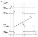
- FIG. It is a timing chart for demonstrating the operation of the test apparatus and the test body in the short circuit test which concerns on Embodiment 1.
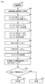
- FIG. It is a flowchart for demonstrating the processing procedure of the semiconductor test method which concerns on Embodiment 1.
- FIG. It is a flowchart for demonstrating the processing procedure of the test method which concerns on Embodiment 2.
- It is a circuit diagram which shows the structure of the semiconductor test apparatus which concerns on Embodiment 3.
- FIG. 1 is a circuit diagram showing a configuration of a semiconductor test apparatus according to the first embodiment.
- the semiconductor test apparatus 110 according to the first embodiment is an apparatus for testing dynamic characteristics such as a short-circuit test of a test body 100 having a semiconductor switching element as a subject.
- the semiconductor test apparatus 110 is also simply referred to as "test apparatus 110".
- the test apparatus 110 includes a DC power supply 30, a control unit 31, a capacitor 32, a switch 33, and probes 41, 42, 43.
- the DC power supply 30 is configured to apply a DC voltage between the main electrodes 51 and 52 of the test piece 100.
- the DC power supply 30 is, for example, a storage battery.
- the power supply voltage of the DC power supply 30 is, for example, about 650V.
- the control unit 31 is electrically connected to the control unit 21 included in the test body 100, and is configured to control the control unit 21 for testing the subject.
- the capacitor 32 and the switch 33 are electrically connected in series between the positive electrode and the negative electrode of the DC power supply 30.
- the capacitor 32 for example, an electrolytic capacitor, a film capacitor, a ceramic capacitor, or the like can be used.
- the capacitor 32 is useful when supplying a current exceeding the supply capacity of the DC power supply 30 to the test piece 100 in a short time. Further, the capacitor 32 makes it possible to smooth the DC voltage of the DC power supply 30.
- the capacitor 32 corresponds to one embodiment of the "second capacitor".
- the switch 33 constitutes a cutoff circuit for cutting off the charging of the capacitor 32 by the DC power supply 30.
- a semiconductor switch or a mechanical switch can be applied to the switch 33.
- the semiconductor switch is typically a semiconductor switching element such as an IGBT or MOSFET.
- the mechanical switch is, for example, a switch such as a relay.
- the switch 33 corresponds to an embodiment of the "first switch".
- the switch 33 is conducted (on) or non-conducted (off) according to the control signal given from the control unit 31. By turning on the switch 33, DC power is supplied from the DC power supply 30 to the capacitor 32, and the capacitor 32 is charged. By turning off the switch 33, the charging of the capacitor 32 is cut off.
- the first terminal is electrically connected to the positive electrode of the DC power supply 30, and the second terminal is electrically connected to the high voltage side main electrode 51 of the test piece 100.
- the first terminal of the probe 42 is electrically connected to the negative electrode of the DC power supply 30, and the second terminal is electrically connected to the low voltage side main electrode 52 of the test piece 100.
- the first terminal is electrically connected to the control unit 31, and the second terminal is electrically connected to the control terminal 53 of the test piece 100.
- the control terminal 53 is electrically connected to the control unit 21.
- the probe 41 corresponds to an embodiment of the "first probe", and the probe 42 corresponds to an embodiment of the "second probe".
- the high-pressure side main electrode 51 corresponds to one embodiment of the “first main electrode”
- the low-pressure side main electrode 52 corresponds to one embodiment of the “second main electrode”.
- the test body 100 is a full-bridge type three-phase inverter that converts DC power input between the high-voltage side main electrode 51 and the low-voltage side main electrode 52 into three-phase AC power as a main circuit.
- the three-phase inverter circuit 150 includes semiconductor switching elements 1 to 6 and diodes 11 to 16.
- Each of the semiconductor switching elements 1 to 6 has a positive electrode, a negative electrode, and a control electrode.
- the semiconductor switching elements 1 to 6 can control the formation (on) and cutoff (off) of the current path between the positive electrode and the negative electrode according to the control signal (voltage or current) input from the control unit 21 to the control electrode. It is composed.
- any self-extinguishing semiconductor element can be applied to the semiconductor switching elements 1 to 6.
- the semiconductor switching element is a MOSFET (Metal-Oxide-Semiconductor Field-Effect Transistor)
- the positive electrode means a drain electrode
- the negative electrode means a source electrode
- the control electrode means a gate electrode.
- the semiconductor switching element is an IGBT (Insulated Gate Transistor)
- the positive electrode means an emitter electrode
- the negative electrode means a collector electrode
- the control electrode means a gate electrode.
- the semiconductor switching element is an IGBT.
- the semiconductor switching elements 1 to 6 are also referred to as IGBTs 1 to 6.
- the emitter electrodes of the IGBTs 1, 3 and 5 are connected to the high-voltage side main electrodes 51, and the collector electrodes of the IGBTs 2, 4 and 6 are connected to the low-voltage side main electrodes 52.
- the collector electrode of the IGBT 1 and the emitter electrode of the IGBT 2 are connected by a U-phase output electrode 25_1.
- the collector electrode of the IGBT 3 and the emitter electrode of the IGBT 4 are connected by a V-phase output electrode 25_2.
- the collector electrode of the IGBT 5 and the emitter electrode of the IGBT 6 are connected by a W phase output electrode 25_3.
- the three-phase output electrode 25 is connected to a load such as a motor and is used to drive the load.
- Diodes 11 to 16 are connected to IGBTs 1 to 6 in antiparallel, respectively, to form a freewheeling diode.
- the built-in body diode can be used as a freewheeling diode.
- As a material constituting the semiconductor switching element in addition to silicon (Si), silicon carbide (SiC) or gallium nitride (GaN), which is a wide bandgap semiconductor, can be applied.
- a sense terminal is connected to each emitter electrode of IGBTs 1 to 6.
- the sense terminal is electrically connected to the control unit 21.
- a current (hereinafter, also referred to as a sense current) obtained by dividing the main current (emitter current) flowing between the collector electrode and the emitter electrode of the corresponding IGBT at a constant ratio (for example, 1/10000) flows through the sense terminal.
- the control unit 21 is configured to control the current flowing through the main electrodes 51 and 52 or the three-phase output electrodes 25_1 to 25_3 of the test body 100 based on the respective sense currents of the IGBTs 1 to 6. For example, when the sense current of the IGBT 1 becomes equal to or higher than the threshold value (for example, 1A or higher), the control unit 21 determines that the main current (emitter current) of the IGBT 1 is an overcurrent, and outputs a control signal for turning off the IGBT 1. Generate. The control unit 21 inputs the generated control signal to the gate electrode of the IGBT 1.
- the threshold value for example, 1A or higher
- Each of IGBTs 1 to 6 is turned on when the control signal input to the gate electrode transitions from the L (logical low) level to the H (logical high) level, and when the control signal transitions from the H level to the L level. Turn off. Each of the IGBTs 1 to 6 may be turned on when the control signal transitions from the H level to the L level, and may be turned off when the control signal transitions from the L level to the H level.
- a function generator (arbitrary waveform generator) can be used for the control unit 21.
- the function of the control unit 21 can be realized by software processing and / or hardware processing by a microcomputer.
- control unit 31 During the test of the test body 100 using the test device 110, the control unit 31 generates a control signal for turning on / off the IGBTs 1 to 6.
- the control unit 21 receives a control signal from the control unit 31 via the probe 43 and the control terminal 53.
- the control unit 21 inputs the received control signal to the gate electrodes of the IGBTs 1 to 6.
- the capacitor 22 is electrically connected between the high voltage side main electrode 51 and the low voltage side main electrode 52.
- the capacitor 22 is a DC voltage smoothing capacitor.
- the capacitor 22 corresponds to one embodiment of the "first capacitor".
- the discharge resistor 23 is a resistor for discharging the wiring of the capacitor 22 and the test body 100 (not shown) and the stray capacitance of the IGBTs 1 to 6. For example, when the test body 100 and the external control circuit that controls the test body 100 are electrically cut off due to disconnection or the like during actual operation, the test body 100 is discharged in order to discharge the charged charge.
- the resistor 23 is used. In this case, it is desirable that the discharge be completed within a few seconds after the disconnection occurs.
- the resistance value of the discharge resistor 23 is about 20 k ⁇ .
- the capacitor 32 is pre-charged using the DC power supply 30 by turning on the switch 33 in the test apparatus 110. As a result, power is supplied to the test body 100 by the charged capacitor 32.
- a high-voltage power supply having a maximum output current of 1 A or less is often used for the DC power supply 30.
- the subject fails while energy is being applied to the subject in the test body 100 from the capacitor 32, the failure of the subject is detected and the switch 33 is quickly turned off, so that the subject and the probe 41 , 42 damage progress can be suppressed.
- the time required for the switch 33 to turn off is often several tens of seconds.
- the applied voltage between the main electrodes 51 and 52 is 650 V
- the capacitance of the capacitor 32 is 10000 ⁇ F
- the resistance component contained in the current path formed between the capacitor 32 and the subject is 0.2 ⁇ .
- a maximum current of 3250 A will continue to flow in the current path for 20 ms. Therefore, when the switch 33 is turned off, all the electric charges accumulated in the capacitor 32 are discharged, which may cause damage to the subject and the probes 41 and 42.
- the switch 33 when a semiconductor switch is used for the switch 33, for example, when an IGBT is used for the switch 33, the time required for the switch 33 to turn off is often several ⁇ s. Therefore, the switch 33 can be turned off to cut off the current path before the charge of the capacitor 32 is completely discharged. However, in general, when a current of several thousand A continues to flow for several ⁇ s, a probe having a rated current of several tens A may be damaged to the extent that it cannot be used continuously.
- the semiconductor test method according to the first embodiment will be described with reference to FIGS. 2 and 3.
- the element to be the subject is IGBT1
- a short-circuit test of IGBT1 is performed as a dynamic characteristic test.
- the IGBTs 1 and the other IGBTs 3 to 6 except the IGBT 2 connected in series with the IGBT 1 are always turned off.
- FIG. 2 is a timing chart for explaining the operation of the test apparatus 110 and the test body 100 in the short-circuit test according to the first embodiment.
- FIG. 2 shows waveforms of the switch 33, the gate voltage of the IGBT 2, the gate voltage of the IGBT 1, the emitter current of the IGBT 1, and the collector-emitter (CE) voltage of the IGBT 1 in this order from the top.
- the switch 33 is also turned off by receiving the L level control signal and turned on by receiving the H level control signal.
- the control unit 31 inputs an H level control signal to the gate electrode of the IGBT 2 through the control unit 21 with the switch 33 held off. As a result, the IGBT 2 is turned on. At this time, since the L level control signal is input to the gate electrode of the IGBT 1, the IGBT 1 is not turned on. Therefore, no current flows between the high-voltage side main electrode 51 and the low-voltage side main electrode 52. In the test device 110, since the switch 33 is turned off, the capacitor 32 is not charged either. Therefore, after the time t0, only the capacitor 22 of the test body 100 is charged.
- the control unit 31 turns on the IGBT 1 by inputting an H level control signal to the gate electrode of the IGBT 1 through the control unit 21.
- the main electrodes 51 and 52 are short-circuited.
- a short-circuit current starts to flow between the main electrodes 51 and 52 due to the electric charge stored in the capacitor 22.
- the short-circuit current flows from the positive electrode of the capacitor 22 to the negative electrode of the capacitor 22 via the IGBT 1 and the IGBT 2 through the current path 61 shown by the solid line in FIG.
- the short-circuit current passes through the current path 62 shown by the broken line in FIG.
- the waveform of the emitter current of the IGBT 1 in FIG. 2 represents the temporal change of the short-circuit current.
- the short-circuit current flowing through the current path 61 and the short-circuit current flowing through the current path 62 are compared, the short-circuit current flowing through the current path 61 is much larger. Therefore, the short-circuit current flowing through the current path 62 can be ignored. This is because, in a general test apparatus, the maximum output current of the DC power supply 30 is often 1 A or less, so that most of the short-circuit current reaching several thousand A at time t2 is supplied from the capacitor 22. Further, the capacitor 22 is built in the same test body 100 as the IGBT 1, while the DC power supply 30 is often installed several meters away from the test body 100.
- the current path 62 contains a large stray inductance as compared with the current path 61, the stray inductance hinders the increase in the current. As a result, a current smaller than the maximum output current of the DC power supply 30 may flow in the current path 62.
- the emitter current (that is, short-circuit current) of the IGBT 1 increases after the time t1.
- the control unit 21 monitors the emitter current of the IGBT 1 based on the sense currents of the IGBT 1 and the IGBT 2. When a sense current equal to or higher than the threshold value is detected at time t2, the control unit 21 shifts the control signal input to the gate electrode of the IGBT 1 from the H level to the L level. As a result, the IGBT 1 is turned off.
- the short mode between the main electrodes 51 and 52 is canceled, so that the emitter current of the IGBT 1 sharply decreases after the time t2 as shown in the waveform k1.
- the collector-emitter voltage of the IGBT 1 increases to the H level as shown in the waveform k3.
- the IGBT 1 is destroyed during the short mode, the IGBT 1 is not turned off at the time t2, so that the emitter current continues to increase even after the time t2 as shown in the waveform k2.
- the collector-emitter voltage of the IGBT 1 is maintained at the L level as shown in the waveform k4.
- the applied voltage between the main electrodes 51 and 52 is 650 V
- the capacitance of the capacitor 22 is 1000 ⁇ F
- the resistance component contained in the current path 61 is 0.2 ⁇
- a short-circuit current of a maximum of 3250 A continues to flow for 2 msec. It will be.
- the capacitance of the capacitor 22 is set to the optimum capacitance according to the specifications of the test body 100, whereas the test device 110 needs to test various semiconductor elements, so that the capacitance of the capacitor 32 is It may be set to 10 times or more the capacitance of the capacitor 22.
- the contact area between the probe and the main electrode is smaller than the total area of the main electrode, so the rated current of the probe is often several tens of amperes. Therefore, as described above, the probes 41 and 42 are burnt out due to the continuous flow of a maximum current of 3250 A, or the probe 41 and the high-voltage side main electrode 51 and / or the probe 42 and the low-voltage side main electrode 52 are fused. There is a risk of As a result, every time the IGBT of the subject is destroyed, the operation of the test device 110 is stopped, and operations such as replacement of the probes 41 and 42 and / or failure confirmation of the test device 110 are required.
- the semiconductor test method according to the first embodiment when the IGBT 1 as a subject is destroyed, a short-circuit current is short-circuited in the current path 61 formed between the capacitor 22 and the IGBTs 1 and 2 inside the test body 100. Therefore, it is possible to prevent a large current from flowing through the test apparatus 110. Therefore, the progress of damage to the test jigs such as probes 41 and 42 in contact with the broken semiconductor element, the damage to the test body 100 caused by the damage to the test jig, and the damage to the test body 100 next to the test body 100. It is possible to suppress poor transportation of the test piece to be tested.
- FIG. 3 is a flowchart for explaining the processing procedure of the semiconductor test method according to the first embodiment.
- FIG. 3 illustrates a processing procedure for a short-circuit test when IGBT1 is used as a subject.
- step S01 when the short-circuit test by the test device 110 is started in step S01, the probes 41 and 42 of the test device 110 are connected to the main electrodes 51 and 52 of the test body 100, respectively, in step S02. As a result, the test body 100 and the test device 110 are electrically connected. Further, by connecting the probe 43 of the test device 110 to the control terminal 53 of the test body 100, the control unit 21 and the control unit 31 are communicably connected. In this state, in step S03, the control unit 31 does not charge the capacitor 32 by holding the switch 33 in the off state.
- step S04 the control unit 21 turns on the IGBT 2 by inputting an H level control signal to the gate electrode of the IGBT 2 in response to a command from the control unit 31.
- step S05 the control unit 31 applies a DC voltage from the DC power supply 30 of the test device 110 to the main electrodes 51 and 52 via the probes 41 and 42. By applying this DC voltage, the capacitor 22 inside the test piece 100 is charged in step S06.
- step S07 the control unit 21 turns on the IGBT 1 by inputting an H level control signal to the gate electrode of the IGBT 1.
- the IGBTs 1 and 2 are turned on, and the main electrodes 51 and 52 are short-circuited.
- the control unit 21 monitors the emitter current of the IGBT 1 based on the sense current of the IGBT 1 and the IGBT 2. When the sense current exceeds the threshold value, the control unit 21 detects the overcurrent of the emitter current of the IGBT 1. In this case, the control unit 21 turns off the IGBT 1 by shifting the control signal input to the gate electrode of the IGBT 1 from the H level to the L level in step S08.
- the control unit 21 determines that the IGBT 1 has been destroyed (YES in S09), and in step S10, the IGBT 1 Judges that the dynamic characteristics of are unacceptable.
- the control unit 21 determines that the IGBT 1 is not destroyed (NO in S09), and in step S11, the dynamic characteristics of the IGBT 1. Is determined to pass.
- the IGBT 1 When performing a short-circuit test using the IGBT 2 as a subject, the IGBT 1 may be replaced with the IGBT 2 and the IGBT 2 may be replaced with the IGBT 1 in the above description. Further, when performing a short-circuit test on the IGBTs of other phases of the three-phase inverter circuit 150, the IGBT 1 may be replaced with the IGBT of the other phase, and the IGBT 2 may be replaced with the IGBT connected in series with the IGBT of the other phase. .. In this way, a short circuit test can be performed on all of the IGBTs 1 to 6 constituting the three-phase inverter circuit 150.
- the capacitor 22 connected between the main electrodes 51 and 52 inside the test body 100 is precharged and stored in the capacitor 22.
- FIG. 4 is a circuit diagram showing the configuration of the semiconductor test apparatus according to the second embodiment.
- the semiconductor test apparatus 110 according to the second embodiment includes a series circuit of the capacitor 32 and the switch 33 as compared with the semiconductor test apparatus 110 according to the first embodiment shown in FIG. The difference is that there is no such thing.
- the capacitor 32 is charged by turning off the switch 33 before applying the DC voltage between the DC power supply 30 and the main electrodes 51 and 52 of the test body 100. Is not performed.
- the test device 110 since the test device 110 does not have the series circuit of the capacitor 32 and the switch 33, the process of turning off the switch 33 becomes unnecessary.
- the operation of the semiconductor test apparatus 110 according to the second embodiment will be described with reference to FIGS. 5 and 6. Also in the second embodiment, as in the first embodiment, the semiconductor element to be the subject is set to the IGBT 1, and the short circuit test of the IGBT 1 is performed. The operation of the semiconductor test device 110 according to the second embodiment will be described only in that it differs from the operation of the semiconductor test device 110 according to the first embodiment described with reference to FIGS. 2 and 3.
- FIG. 5 is a timing chart for explaining the operation of the test apparatus 110 and the test body 100 in the short circuit test according to the second embodiment.
- FIG. 5 shows waveforms of the gate voltage of the IGBT 2, the gate voltage of the IGBT 1, the emitter current of the IGBT 1, and the collector-emitter voltage of the IGBT 1 in this order from the top. That is, the timing chart of FIG. 5 is equivalent to the timing chart of FIG. 2 excluding the waveform of the switch 33.
- FIG. 6 is a flowchart for explaining the processing procedure of the test method according to the second embodiment.
- the flowchart of FIG. 6 is equivalent to the flowchart shown in FIG. 3 excluding the process of step S03 (process of holding the switch 33 in the off state).
- the short circuit current is caused by the electric charge accumulated in the capacitor 22 due to the short circuit between the main electrodes 51 and 52. Begins to flow. Since most of the short-circuit current at this time flows through the current path 61 shown in FIG. 4, it is possible to prevent a large current from flowing through the test apparatus 110. Therefore, the same effects as those of the semiconductor test apparatus and test method according to the first embodiment can be obtained.
- FIG. 7 is a circuit diagram showing the configuration of the semiconductor test apparatus according to the third embodiment.
- the semiconductor test apparatus 110 according to the third embodiment has a different configuration of the test body 100 as compared with the semiconductor test apparatus 110 according to the first embodiment shown in FIG.
- the test body 100 according to the second configuration example shown in FIG. 7 includes an IGBT 1, a diode 11, and a capacitor 22.
- the emitter electrode of the IGBT 1 is connected to the high pressure side main electrode 51, and the collector electrode of the IGBT 1 is connected to the low pressure side main electrode 52.
- the diode 11 is connected to the IGBT 1 in antiparallel.
- the sense terminal (not shown) of the IGBT 1 is electrically connected to the control unit 21.
- the capacitor 22 is electrically connected in parallel with the IGBT 1 between the high voltage side main electrode 51 and the low voltage side main electrode 52.
- the short-circuit test of the object object IGBT1 can be executed according to the flowchart shown in FIG.
- the process of step S04 can be omitted. That is, while the test apparatus 110 is connected between the main electrodes 51 and 52 of the test body 100 (S01 in FIG. 3) and the switch 33 is held in the off state (S03 in FIG. 3), direct current is applied between the main electrodes 51 and 52. A voltage is applied (S05 in FIG. 3). When the capacitor 22 is charged in response to this DC voltage (S06 in FIG. 3), the control unit 21 turns on the IGBT 1 (S07 in FIG.
- the control unit 21 turns off the IGBT 1 (S08 in FIG. 3) and determines whether or not the IGBT 1 is destroyed based on the sense current after the turn-off (FIG. 3). S09).
- FIG. 8 is a circuit diagram showing the configuration of the semiconductor test apparatus according to the fourth embodiment.
- the semiconductor test apparatus 110 according to the fourth embodiment has a different structure of the test body as compared with the semiconductor test apparatus 110 according to the first embodiment shown in FIG.
- the test body 200 according to the third configuration example is a test body 100 according to the first configuration example shown in FIG. 1 in which a boost converter circuit 210 is added to the DC side of the three-phase inverter circuit 150.
- the boost converter circuit 210 includes semiconductor switching elements 7 and 8, diodes 17 and 18, a reactor 81, and input electrodes 91 and 92.
- each of the semiconductor switching elements 7 and 8 has a positive electrode, a negative electrode, and a control electrode, and controls on / off according to a control signal applied to the control electrode from the control unit 21. It is configured to be possible.
- the semiconductor switching elements 7 and 8 are IGBTs.
- the semiconductor switching elements 7 and 8 are also referred to as IGBTs 7 and 8.
- the input electrodes 91 and 92 correspond to one embodiment of the "first input electrode" and the "second input electrode".
- the emitter electrode of the IGBT 7 is connected to the high voltage side main electrode 51, and the emitter electrode of the IGBT 8 is connected to the low voltage side main electrode 52 and the low voltage side input electrode 92.
- the emitter electrode of the IGBT 7 and the collector electrode of the IGBT 8 are connected to the first terminal of the reactor 81.
- the second terminal of the reactor 81 is connected to the high voltage side input electrode 91.
- the test body 200 boosts the DC voltage applied between the input electrodes 91 and 92 to a voltage at which a load (for example, a motor) connected to the three-phase output electrode 25 can be driven by the boost converter circuit 210.
- the boosted voltage is converted into a three-phase AC voltage by the three-phase inverter circuit 150 and supplied to the load.
- the control unit 21 calculates a duty ratio for setting the output voltage of the boost converter circuit 210 to the target voltage, and turns on / off the IGBTs 7 and 8 of the boost converter circuit 210 based on the calculated duty ratio. Generate a control signal for control.
- the control unit 21 further generates a control signal for controlling the on / off of the IGBTs 1 to 6 of the three-phase inverter circuit 150.
- the control unit 21 inputs the generated control signal to the control electrodes of the IGBTs 1 to 8.
- the test apparatus 110 can perform a short-circuit test of the IGBTs 1 to 6 constituting the three-phase inverter circuit 150 by using the semiconductor test method according to the first embodiment.
- FIG. 9 is a circuit diagram showing the configuration of the semiconductor test apparatus according to the fifth embodiment.
- the semiconductor test apparatus 110 according to the fifth embodiment has a connection relationship of the test apparatus 110 to the test body 200 as compared with the semiconductor test apparatus 110 according to the fifth embodiment shown in FIG. different.
- the semiconductor test apparatus 110 is connected between the input electrodes 91 and 92 of the test body 200. Specifically, the probe 41 is connected to the high pressure side input electrode 91, and the probe 42 is connected to the low pressure side input electrode 92.
- FIG. 10 is a flowchart for explaining the processing procedure of the semiconductor test method according to the fifth embodiment.
- FIG. 10 illustrates a processing procedure for a short-circuit test when IGBT1 is used as a subject.
- step S051 the control unit 21 boosts the DC voltage applied between the input electrodes 91 and 92 to a target voltage (for example, 650V) by controlling the on / off of the IGBTs 7 and 8 constituting the boost converter circuit 210.
- a DC voltage for testing for example, 650V is generated between the main electrodes 51 and 52.
- step S06 the capacitor 22 inside the test piece 200 is charged by receiving the DC voltage generated between the main electrodes 51 and 52.
- the control unit 21 turns on the IGBT 1 (S07) and detects the short-circuit current based on the sense current of the IGBT 1.
- the control unit 21 turns off the IGBT 1 (S08) and determines whether or not the IGBT 1 is destroyed based on the sense current after the turn-off (S08).
- the avalanche test of the test body 200 can be performed.
- the avalanche test is the avalanche destruction caused by the energy stored in the reactor flowing at once between the positive and negative electrodes at the moment when the control signal input to the control electrode of the semiconductor switching element is changed from the H level to the L level. This is a test for evaluating resistance to.
- FIG. 11 illustrates the processing procedure of the avalanche test when IGBT1 is used as a subject.
- step S03 when the avalanche test by the test apparatus 110 is started in the same steps S01 to S03 as in FIG. 3, the probes 41 and 42 of the test apparatus 110 are attached to the main electrodes 51 and 52 of the test body 100, respectively. By connecting, the test body 100 and the test device 110 are electrically connected. In this state, in step S03, the capacitor 32 is not charged by holding the switch 33 in the off state.
- step S041 the control unit 21 turns on the IGBT 1 and the IGBT 2 by inputting an H level control signal to the respective gate electrodes of the IGBT 1 and the IGBT 2.
- the control unit 21 boosts the DC voltage applied between the input electrodes 91 and 92 by controlling the on / off of the IGBTs 7 and 8 constituting the boost converter circuit 210 in step S051, and between the main electrodes 51 and 52. Generate a test voltage (eg 650V).
- step S06 the capacitor 22 inside the test piece 200 is charged by receiving the DC voltage generated between the main electrodes 51 and 52. Further, in step S061, energy is stored in the reactor 81.
- the control unit 21 turns off the IGBT 1 by inputting an L level control signal to the gate electrode of the IGBT 1 in step S071.
- the collector-emitter voltage of the IGBT 1 rises to the avalanche voltage of the IGBT due to the energy stored in the reactor 81.
- the IGBT 1 enters the avalanche mode.
- the energy stored in the reactor 81 is consumed by the IGBT 1, so that the emitter current of the IGBT 1 decreases. If the avalanche destruction does not occur in the IGBT 1, the avalanche mode continues until all the energy stored in the reactor 81 is released, and the avalanche mode ends when the emitter current becomes 0.
- the collector-emitter voltage of the IGBT 1 decreases to near 0V. Therefore, the reactor 81 starts to store magnetic energy again, and the emitter current of the IGBT 1 starts to rise.
- the control unit 21 monitors the emitter current of the IGBT 1 for a reference time based on the sense current of the IGBT 1 in step S09.
- the reference time can be set based on the result of dividing the inductance value of the reactor 81 by the difference between the avalanche voltage of the IGBT 1 and the power supply voltage.
- the control unit 21 determines in step S10 that the dynamic characteristics of the IGBT 1 have failed. do.
- the control unit 21 determines that the avalanche destruction of the IGBT 1 has not occurred (NO in S09), and determines that the dynamic characteristics of the IGBT 1 have passed in step S11. do.
- the capacitor 22 connected between the main electrodes 51 and 52 is charged inside the test body 200, and the energy stored in the capacitor 22 is charged.
- FIG. 12 is a circuit diagram showing the configuration of the semiconductor test apparatus according to the sixth embodiment.
- the semiconductor test apparatus 110 according to the sixth embodiment has a different structure of the test body as compared with the semiconductor test apparatus 110 according to the first embodiment shown in FIG.
- the test body 200 includes a boost converter circuit 210, switches 160 and 161, discharge resistors 163, and input electrodes 91 and 92.
- a test device 110 is connected between the input electrodes 91 and 92.
- the power supply voltage VD of the DC power supply 30 included in the test device 110 is, for example, about 500V.
- the boost converter circuit 210 is called a multi-level chopper.
- the boost converter circuit 210 includes semiconductor switching elements 7 to 10, diodes 17 to 20, a reactor 81, and capacitors 24 and 25.
- each of the semiconductor switching elements 7 to 10 has a positive electrode, a negative electrode, and a control electrode, and controls on / off according to a control signal applied to the control electrode from the control unit 21. It is configured to be possible.
- the semiconductor switching elements 7 to 10 are IGBTs. In the following description, the semiconductor switching elements 7 to 10 are also referred to as IGBTs 7 to 10.
- the IGBTs 7 to 10 are connected in series between the high voltage side main electrode 51 and the low voltage side main electrode 52.
- the collector electrode of the IGBT 7 is connected to the high voltage side main electrode 51.
- the emitter electrode of the IGBT 8 and the collector electrode of the IGBT 9 are connected to the first terminal of the reactor 81.
- the second terminal of the reactor 81 is connected to the high voltage side input electrode 91.
- the emitter electrode of the IGBT 10 is connected to the low pressure side main electrode 52 and the low pressure side input electrode 92.
- the IGBTs 7 to 10 correspond to one embodiment of the "first semiconductor element", the "second semiconductor element", the "third semiconductor element", and the "fourth semiconductor element", respectively.
- the first terminal of the capacitor 24 is connected to the second terminal of the reactor 81 and the high voltage side input electrode 91, and the second terminal is connected to the low voltage side input electrode 92.
- the capacitor 24 is a smoothing capacitor for reducing voltage fluctuations between the input electrodes 91 and 92.
- the first terminal of the capacitor 25 is connected to the emitter electrode of the IGBT 7 and the collector electrode of the IGBT 8, and the second terminal is connected to the emitter electrode of the IGBT 9 and the collector electrode of the IGBT 10.
- the capacitor 25 is a charge pump configured to superimpose a voltage on an input voltage and boost the voltage by transitioning the stored electric charge.
- the capacitor 25 corresponds to one embodiment of the "third capacitor”.
- the first terminal of the switch 161 is connected to the high voltage side input electrode 91, and the second terminal is connected to the second terminal of the reactor 81.
- the switch 161 corresponds to an embodiment of the "second switch”.
- the switch 160 and the discharge resistor 163 are connected in series between the second terminal of the switch 161 and the low voltage side input electrode 92.
- the test body 200 boosts the DC voltage applied between the input electrodes 91 and 92 to a voltage at which the load connected between the main electrodes 51 and 52 can be driven by the boost converter circuit 210.
- Is configured to supply the load.
- the control unit 21 calculates a duty ratio for setting the output voltage of the boost converter circuit 210 to the target voltage, and turns on / off the IGBTs 7 to 10 of the boost converter circuit 210 based on the calculated duty ratio. Generate a control signal for control.
- the control unit 21 inputs the generated control signal to the control electrodes of the IGBTs 7 to 10.
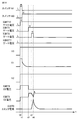
- FIG. 13 is a timing chart for explaining the operation of the test apparatus 110 and the test body 200 in the short-circuit test according to the sixth embodiment.
- the switch 161 and the switch 160 the gate voltage of the IGBT 10, the gate voltage of the IGBT 7, the terminal voltage V0 of the capacitor 25, the terminal voltage V1 of the capacitor 24, the terminal voltage V2 of the capacitor 22, and the IGBT 10
- the waveforms of the collector-emitter (CE-to-CE) voltage, the CE-to-CE voltage of the IGBT 7, and the emitter current of the IGBT 7 are shown.
- the switches 161, 160 are also turned off by receiving the L level control signal and turned on by receiving the H level control signal, similarly to the IGBT.
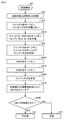
- FIG. 14 is a flowchart for explaining the processing procedure of the short-circuit test when the IGBT 7 is used as the subject.
- the semiconductor test method according to the sixth embodiment will be described with reference to FIGS. 13 and 14.
- step S21 when the short-circuit test by the test device 110 is started in step S21, the probes 41 and 42 of the test device 110 are connected to the input electrodes 91 and 92 of the test body 200, respectively, in step S22.
- the test body 200 and the test device 110 are electrically connected to each other.
- the control unit 21 and the control unit 31 are communicably connected. In this state, in step S23, the control unit 31 does not charge the capacitor 32 by holding the switch 33 in the off state.
- step S24 the control unit 21 receives a command from the control unit 31 and inputs an H level control signal to the switch 161 to turn on the switch 161 (time t0 in FIG. 13).
- the control unit 21 turns off the switch 161 and turns on the switch 160 in step S25 (time t1 in FIG. 13). By turning off the switch 161 the test body 200 and the test device 110 are electrically cut off. When the switch 160 is turned on in this state, the discharge of the capacitor 24 is started. On the other hand, the diode 17 does not discharge the capacitor 22.
- step S26 the control unit 21 turns on the IGBT 10 by inputting an H level control signal to the gate electrode of the IGBT 10 in response to a command from the control unit 31 (time t2 in FIG. 13).
- the voltage between CEs of the IGBT 7 DC voltage VD.
- the control unit 21 receives a command from the control unit 31 and inputs an H level control signal to the gate electrode of the IGBT 7 to turn on the IGBT 7 (time in FIG. 13). t3).
- step S28 When both the IGBTs 7 and 10 are turned on and the main electrodes 51 and 52 are short-circuited (short-circuited), the discharge of the capacitor 22 is started in step S28.
- a short-circuit current begins to flow between the main electrodes 51 and 52 due to the electric charge stored in the capacitor 22.
- the short-circuit current flows from the positive electrode of the capacitor 22 to the negative electrode of the capacitor 22 via the IGBT 7, the capacitor 25 and the IGBT 10 through the current path 160 shown by the solid line in FIG.
- the control unit 21 monitors the emitter current of the IGBT 7 based on the sense current of the IGBT 7. When the sense current exceeds the threshold value, the control unit 21 detects the overcurrent of the IGBT 7. In this case, the control unit 21 turns off the IGBT 7 by shifting the control signal input to the gate electrode of the IGBT 7 from the H level to the L level in step S29 (time t4 in FIG. 13).
- the control unit 21 determines that the IGBT 7 has been destroyed (YES in S30), and in step S31, the IGBT 7 Judges that the dynamic characteristics of are unacceptable.
- the control unit 21 determines that the IGBT 7 has not been destroyed (NO in S30), and in step S32, the dynamic characteristics of the IGBT 7. Is determined to pass.
- the IGBT 7 When performing a short-circuit test using the IGBT 10 as a subject, the IGBT 7 may be replaced with the IGBT 10 and the IGBT 10 may be replaced with the IGBT 7 in the above description. However, if the capacitor 24 is not discharged at the time t1 of FIG. 13, the capacitor 25 will be charged at the time t2, so that the short-circuit test cannot be performed.
- FIG. 15 is a timing chart for explaining the operation of the test apparatus 110 and the test body 200 in the short circuit test according to the sixth embodiment.
- the switch 161 and the switch 160 in order from the top, the switch 161 and the switch 160, the gate voltage of the IGBT 10, the gate voltage of the IGBT 9, the gate voltage of the IGBT 8, the gate voltage of the IGBT 7, the terminal voltage V0 of the capacitor 25, and the terminal voltage V1 of the capacitor 24, The waveforms of the terminal voltage V2 of the capacitor 22, the CE voltage of the IGBT 9, the CE voltage of the IGBT 8, and the emitter current of the IGBT 8 are shown.
- the switches 161, 160 are also turned off by receiving the L level control signal and turned on by receiving the H level control signal, similarly to the IGBT.
- FIG. 16 is a flowchart for explaining the processing procedure of the short-circuit test when the IGBT 8 is used as the subject.
- the semiconductor test method according to the sixth embodiment will be described with reference to FIGS. 15 and 16.
- step S21 when the short-circuit test by the test device 110 is started in step S21, the probes 41 and 42 of the test device 110 are connected to the input electrodes 91 and 92 of the test body 200, respectively, in step S22.
- the test body 200 and the test device 110 are electrically connected to each other.
- the control unit 21 and the control unit 31 are communicably connected. In this state, in step S23, the control unit 31 does not charge the capacitor 32 by holding the switch 33 in the off state.
- step S240 the control unit 21 turns on the switch 161 by inputting an H level control signal to the switch 161 in response to a command from the control unit 31. Further, the control unit 21 turns on the IGBT 10 by inputting an H level control signal to the gate electrode of the IGBT 10 in response to a command from the control unit 31 (time t0 in FIG. 15).
- the control unit 21 turns off the switch 161 and turns on the switch 160 in step S25 (time t1 in FIG. 15).
- the switch 160 is turned on instead of the switch 161, the discharge of the capacitor 24 is started.
- the diode 17 does not discharge the capacitor 22. Further, the diode 18 does not discharge the capacitor 25.
- step S260 the control unit 21 turns on the IGBT 9 by inputting an H level control signal to the gate electrode of the IGBT 9 in response to a command from the control unit 31 (time t2 in FIG. 15).
- the voltage between CEs of the IGBT 8 DC voltage VD.
- step S270 the control unit 21 turns on the IGBT 8 by inputting an H level control signal to the gate electrode of the IGBT 8 in response to a command from the control unit 31 (time in FIG. 15). t3).
- step S28 When both the IGBTs 8 and 9 are turned on and the terminals of the capacitor 25 are short-circuited, the discharge of the capacitor 25 is started in step S28.
- a short-circuit current begins to flow in the IGBTs 8 and 9 due to the electric charge stored in the capacitor 25.
- the short-circuit current flows from the positive electrode of the capacitor 25 to the negative electrode of the capacitor 25 via the IGBT 8 and the IGBT 9 through the current path 161 shown by the broken line in FIG.
- the control unit 21 monitors the emitter current of the IGBT 8 based on the sense current of the IGBT 8. When the sense current exceeds the threshold value, the control unit 21 detects the overcurrent of the IGBT 8. In this case, the control unit 21 turns off the IGBT 8 by shifting the control signal input to the gate electrode of the IGBT 8 from the H level to the L level in step S290 (time t4 in FIG. 15).
- the control unit 21 determines that the IGBT 8 has been destroyed (YES in S300), and in step S31, the IGBT 8 Judges that the dynamic characteristics of are unacceptable.
- the control unit 21 determines that the IGBT 8 has not been destroyed (NO in S300), and in step S32, the dynamic characteristics of the IGBT 8 Is determined to pass.
- the IGBT 8 When performing a short-circuit test using the IGBT 9 as a subject, the IGBT 8 may be replaced with the IGBT 9 and the IGBT 9 may be replaced with the IGBT 8 in the above description.
- a multi-level chopper including IGBTs 7 to 10 connected in series between the main electrodes 51 and 52 and a capacitor 25 for a charge pump.
- the capacitor 22 connected between the main electrodes 51 and 52 is charged inside the test body 200 having the above, and the energy stored in the capacitor 22 is used to execute the test of the IGBT 7 or the IGBT 10.
- a short-circuit failure occurs, it is possible to prevent a large current from flowing through the test apparatus.
- the control unit 31 can be configured by using the function generator 310 and the pulse generator 312 as shown in FIG.
- the function generator 310 generates a signal voltage having a desired waveform and / or a desired frequency.
- the pulse generator 312 generates a control signal for controlling the three-phase inverter circuit 150 (including the boost converter circuit 210) of the test piece 100 (or 200) based on the signal voltage generated by the function generator 310.
- the generated control signal is transmitted to the control unit 21.
- control unit 31 can have a processor 314, a memory 316, an input / output interface (I / F) 318, and a communication I / F 320. Each of these parts is communicably connected to each other via a bus (not shown).
- the processor 314 is typically an arithmetic processing unit such as a CPU (Central Processing Unit) or an MPU (Micro Processing Unit).
- the processor 314 controls the operation of each part of the test apparatus 110 by reading and executing the program stored in the memory 316.
- non-volatile memory such as memory 316, RAM (Random Access Memory), ROM (Read Only Memory) and flash memory.
- the memory 316 stores a program executed by the processor 314, data used by the processor 314, and the like.
- the input / output I / F 318 is an interface for exchanging various data between the processor 314 and the display unit 324 and the input unit 322.
- the display unit 324 is composed of a liquid crystal panel or the like capable of displaying an image.
- the input unit 322 receives the user's operation input to the test device 110.
- the input unit 322 is typically composed of a touch panel, a keyboard, a mouse, and the like.
- the communication I / F 320 is a communication interface for exchanging various data between the test device 110 and other devices including the test bodies 100 and 200, and is realized by an adapter or a connector.
- the communication method may be a wireless communication method using a wireless LAN (Local Area Network) or the like, or a wired communication method using USB (Universal Serial Bus) or the like.
- Embodiment 7 a method of manufacturing the semiconductor device that becomes the test bodies 100 and 200 in the above-described first to sixth embodiments will be described.
- the seventh embodiment describes a method for manufacturing a semiconductor device, which includes the semiconductor test methods according to the first to fifth embodiments in the manufacturing process.
- the semiconductor device manufactured by this manufacturing method has a semiconductor switching element, and includes a first configuration example (see FIG. 1), a second configuration example (see FIG. 7), a third configuration example (see FIG. 8), and a third configuration example (see FIG. 8).
- Specimens 100 and 200 of the fourth configuration example can be applied.
- the semiconductor device is the test body 100 (see FIG. 1) of the first configuration example. That is, the semiconductor device has a full-bridge type three-phase inverter circuit 150, a control unit 21, a capacitor 22, and a discharge resistor 23.
- FIG. 19 is a flowchart for explaining a method of manufacturing a semiconductor device according to the sixth embodiment.
- the semiconductor device manufacturing method includes a step of assembling the semiconductor device (S100), a step of testing the dynamic characteristics of the assembled semiconductor device (S200), and commercializing a semiconductor device that has passed the test. It includes a step (S300).
- the step of manufacturing the three-phase inverter circuit 150 (S110), the step of manufacturing the control unit 21 (S120), the manufactured three-phase inverter circuit 150, the control unit 21, the discharge resistor 23, and so on. It includes a step of mounting the capacitor 22 (S130) and a step of wiring between the mounted three-phase inverter circuit 150, the control unit 21, the discharge resistor 23, and the capacitor 22 (S140).
- semiconductor switching elements (IGBTs) 1 to 6 and diodes 11 to 16 are mounted on the substrate.
- control unit 21 In the step of manufacturing the control unit 21 (S120), a function generator (or microcomputer) constituting the control unit 21, a gate drive circuit of a semiconductor switching element, and the like are mounted on the substrate.
- the substrate on which the three-phase inverter circuit 150 is manufactured and the substrate on which the control unit 21 is manufactured are mounted on the housing of the semiconductor device.
- a discharge resistor 23 and a capacitor 22 are further mounted on the housing.
- the three-phase inverter circuit 150, the control unit 21, the discharge resistance 23, and the capacitor 22 are connected by wiring between the electrodes, the discharge resistance 23, and the capacitor 22 on the substrate mounted on the housing. Are electrically connected to each other. As a result, the semiconductor device (test body 100) shown in FIG. 1 is assembled.
- a test for confirming the functions of the individually manufactured three-phase inverter circuit 150, the control unit 21, and the like is carried out, and those that pass the test are mounted on the housing of the semiconductor device.
- the configuration is to be used.
- the three-phase inverter circuit 150 and the control unit 21 may not be manufactured individually, but these components may be manufactured directly in the housing of the semiconductor device.
- the work of testing each component can be omitted, so that the man-hours can be reduced, but the defect rate may be deteriorated. Therefore, it is sufficient to compare the increase in the cost rate due to the increase in man-hours with the increase in the cost rate due to the deterioration of the defective rate, and adopt a configuration in which the increase is small.
- a characteristic test is executed using the assembled semiconductor device as a test body.
- the characteristic test of the semiconductor device is performed according to the processing procedure described with reference to FIG. That is, when the semiconductor test device 110 (see FIG. 1) is electrically connected to the semiconductor device, a test (short-circuit test or the like) of the dynamic characteristics of the semiconductor switching element to be the subject is executed.
- step of commercializing first, it is determined whether the test result in the step of testing (S200) passes or fails (S310).
- a step (S320) of attaching the upper lid to the housing is performed on the semiconductor device whose test result is acceptable (YES in S310).
- the housing of the semiconductor device is sealed to become a product.
- the semiconductor device whose test result is unacceptable NO in S310
- the commercialized semiconductor device is shipped by the shipping process (S330).
- a capacitor connected between the main electrodes 51 and 52 inside the semiconductor device. 22 is charged in advance, and the characteristic test of the subject is executed using the energy stored in the capacitor 22. This makes it possible to prevent a large current from flowing through the semiconductor test apparatus when the subject is destroyed during the test. As a result, it is possible to suppress the progress of damage to the semiconductor test apparatus due to the breaking current of the semiconductor element.
- each embodiment can be combined, and each embodiment can be appropriately modified or omitted.
Landscapes
- Physics & Mathematics (AREA)
- General Physics & Mathematics (AREA)
- Testing Of Individual Semiconductor Devices (AREA)
Priority Applications (3)
| Application Number | Priority Date | Filing Date | Title |
|---|---|---|---|
| CN202180030989.9A CN115461630B (zh) | 2019-08-29 | 2021-02-25 | 半导体试验装置、半导体试验方法以及半导体装置的制造方法 |
| JP2022518626A JP7370459B2 (ja) | 2019-08-29 | 2021-02-25 | 半導体試験装置、半導体試験方法および半導体装置の製造方法 |
| US17/912,880 US12287355B2 (en) | 2019-08-29 | 2021-02-25 | Semiconductor testing device, semiconductor testing method, and manufacturing method for semiconductor device |
Applications Claiming Priority (3)
| Application Number | Priority Date | Filing Date | Title |
|---|---|---|---|
| JP2019156499 | 2019-08-29 | ||
| JP2020-080885 | 2020-05-01 | ||
| JP2020080885A JP2021039086A (ja) | 2019-08-29 | 2020-05-01 | 半導体試験装置、半導体試験方法および半導体装置の製造方法 |
Publications (1)
| Publication Number | Publication Date |
|---|---|
| WO2021220602A1 true WO2021220602A1 (ja) | 2021-11-04 |
Family
ID=74846987
Family Applications (1)
| Application Number | Title | Priority Date | Filing Date |
|---|---|---|---|
| PCT/JP2021/007166 Ceased WO2021220602A1 (ja) | 2019-08-29 | 2021-02-25 | 半導体試験装置、半導体試験方法および半導体装置の製造方法 |
Country Status (4)
| Country | Link |
|---|---|
| US (1) | US12287355B2 (https=) |
| JP (2) | JP2021039086A (https=) |
| CN (1) | CN115461630B (https=) |
| WO (1) | WO2021220602A1 (https=) |
Citations (8)
| Publication number | Priority date | Publication date | Assignee | Title |
|---|---|---|---|---|
| JPH0836019A (ja) * | 1994-07-22 | 1996-02-06 | Sony Tektronix Corp | 特性測定装置 |
| JP2008545949A (ja) * | 2005-03-22 | 2008-12-18 | フォームファクター, インコーポレイテッド | 電圧故障検出保護 |
| JP2010276477A (ja) * | 2009-05-28 | 2010-12-09 | Fuji Electric Systems Co Ltd | 半導体チップの試験装置および試験方法 |
| JP2013024794A (ja) * | 2011-07-25 | 2013-02-04 | Honda Motor Co Ltd | 半導体検査装置及び半導体検査方法 |
| JP2014175643A (ja) * | 2013-03-13 | 2014-09-22 | Sharp Corp | 半導体トランジスタのテスト方法 |
| US20160025802A1 (en) * | 2014-07-25 | 2016-01-28 | Thierry Sicard | Systems and methods for test circuitry for insulated-gate bipolar transistors |
| WO2016208141A1 (ja) * | 2015-06-25 | 2016-12-29 | 株式会社デンソー | 半導体素子の検査装置および検査方法 |
| JP2017020811A (ja) * | 2015-07-07 | 2017-01-26 | 株式会社デンソー | 半導体素子の検査回路および検査方法 |
Family Cites Families (12)
| Publication number | Priority date | Publication date | Assignee | Title |
|---|---|---|---|---|
| JPH09162255A (ja) * | 1995-12-06 | 1997-06-20 | Fuji Electric Co Ltd | 半導体素子の試験装置 |
| JPH10197594A (ja) * | 1997-01-10 | 1998-07-31 | Fuji Electric Co Ltd | 半導体試験装置 |
| JP2005124345A (ja) | 2003-10-20 | 2005-05-12 | Nissan Motor Co Ltd | 電力変換装置 |
| JP4687086B2 (ja) | 2004-12-03 | 2011-05-25 | トヨタ自動車株式会社 | 電力変換器の試験装置および試験方法 |
| JP5320953B2 (ja) * | 2008-10-02 | 2013-10-23 | 日産自動車株式会社 | 組電池の性能検出装置及び制御装置 |
| JP2011097799A (ja) * | 2009-11-02 | 2011-05-12 | Yokogawa Electric Corp | 電源装置および半導体試験装置 |
| JP2012229971A (ja) | 2011-04-26 | 2012-11-22 | Honda Motor Co Ltd | 半導体検査装置、及び半導体検査方法 |
| JP6207265B2 (ja) * | 2013-07-04 | 2017-10-04 | 三菱電機株式会社 | 半導体試験装置 |
| US9917335B2 (en) * | 2014-08-28 | 2018-03-13 | Apple Inc. | Methods for determining and controlling battery expansion |
| CN104538694B (zh) * | 2014-12-12 | 2017-02-22 | 中国科学院电工研究所 | 基于电阻抗成像技术的锂电池组监测系统及监测方法 |
| CN211123134U (zh) * | 2019-09-09 | 2020-07-28 | 国网山东省电力公司金乡县供电公司 | 一种igbt特性测试装置 |
| CN217719732U (zh) * | 2021-12-30 | 2022-11-01 | 无边界(苏州)新材料科技有限公司 | 一种电池安全监测装置及电池 |
-
2020
- 2020-05-01 JP JP2020080885A patent/JP2021039086A/ja active Pending
-
2021
- 2021-02-25 CN CN202180030989.9A patent/CN115461630B/zh active Active
- 2021-02-25 US US17/912,880 patent/US12287355B2/en active Active
- 2021-02-25 WO PCT/JP2021/007166 patent/WO2021220602A1/ja not_active Ceased
- 2021-02-25 JP JP2022518626A patent/JP7370459B2/ja active Active
Patent Citations (8)
| Publication number | Priority date | Publication date | Assignee | Title |
|---|---|---|---|---|
| JPH0836019A (ja) * | 1994-07-22 | 1996-02-06 | Sony Tektronix Corp | 特性測定装置 |
| JP2008545949A (ja) * | 2005-03-22 | 2008-12-18 | フォームファクター, インコーポレイテッド | 電圧故障検出保護 |
| JP2010276477A (ja) * | 2009-05-28 | 2010-12-09 | Fuji Electric Systems Co Ltd | 半導体チップの試験装置および試験方法 |
| JP2013024794A (ja) * | 2011-07-25 | 2013-02-04 | Honda Motor Co Ltd | 半導体検査装置及び半導体検査方法 |
| JP2014175643A (ja) * | 2013-03-13 | 2014-09-22 | Sharp Corp | 半導体トランジスタのテスト方法 |
| US20160025802A1 (en) * | 2014-07-25 | 2016-01-28 | Thierry Sicard | Systems and methods for test circuitry for insulated-gate bipolar transistors |
| WO2016208141A1 (ja) * | 2015-06-25 | 2016-12-29 | 株式会社デンソー | 半導体素子の検査装置および検査方法 |
| JP2017020811A (ja) * | 2015-07-07 | 2017-01-26 | 株式会社デンソー | 半導体素子の検査回路および検査方法 |
Also Published As
| Publication number | Publication date |
|---|---|
| CN115461630A (zh) | 2022-12-09 |
| JP2021039086A (ja) | 2021-03-11 |
| JPWO2021220602A1 (https=) | 2021-11-04 |
| US20230141552A1 (en) | 2023-05-11 |
| CN115461630B (zh) | 2025-05-09 |
| JP7370459B2 (ja) | 2023-10-27 |
| US12287355B2 (en) | 2025-04-29 |
Similar Documents
| Publication | Publication Date | Title |
|---|---|---|
| CN110337784B (zh) | 半导体装置及电力转换系统 | |
| CN108173418B (zh) | 半导体装置和电力转换设备 | |
| JP6369808B2 (ja) | 駆動装置、電力変換装置 | |
| JP7140045B2 (ja) | 駆動回路 | |
| JP5692185B2 (ja) | 半導体モジュール | |
| WO2020116133A1 (ja) | 絶縁抵抗検出装置 | |
| KR101538094B1 (ko) | 인버터 시스템의 스위칭 소자 고장 검출 장치 및 방법 | |
| US10587184B2 (en) | Charge pump circuit driving a load connection switch | |
| JP2020182334A (ja) | 駆動回路 | |
| JP2009213305A (ja) | 電力変換装置 | |
| JP2015070678A (ja) | 直流電源装置、直流電源装置の制御方法 | |
| JP6785268B2 (ja) | 誘導性フライバック電源による信号に基づく点火 | |
| CN104247263A (zh) | 电力变换器 | |
| JP7304825B2 (ja) | 半導体試験装置、半導体試験方法および半導体装置の製造方法 | |
| CN109962511B (zh) | 半导体装置 | |
| KR20100029021A (ko) | 플라이백식 승압 회로 및 그것을 이용한 스트로브 장치 | |
| WO2021220602A1 (ja) | 半導体試験装置、半導体試験方法および半導体装置の製造方法 | |
| CN108702015B (zh) | 放电电路以及蓄电装置 | |
| JP6898028B2 (ja) | Dc/dcコンバータ及び電力供給方法 | |
| KR20160071842A (ko) | 게이트 구동부 및 그의 구동방법 | |
| JP6201447B2 (ja) | 電力変換装置及び電力変換装置の制御方法 | |
| JP5724606B2 (ja) | 昇圧型チョッパ回路および昇圧型チョッパ回路の設計方法 | |
| JP2011055633A (ja) | 電源装置 | |
| JP2021065039A (ja) | スイッチの駆動装置 | |
| JP2019180110A (ja) | 電力変換装置 |
Legal Events
| Date | Code | Title | Description |
|---|---|---|---|
| 121 | Ep: the epo has been informed by wipo that ep was designated in this application |
Ref document number: 21796886 Country of ref document: EP Kind code of ref document: A1 |
|
| ENP | Entry into the national phase |
Ref document number: 2022518626 Country of ref document: JP Kind code of ref document: A |
|
| NENP | Non-entry into the national phase |
Ref country code: DE |
|
| 122 | Ep: pct application non-entry in european phase |
Ref document number: 21796886 Country of ref document: EP Kind code of ref document: A1 |
|
| WWG | Wipo information: grant in national office |
Ref document number: 17912880 Country of ref document: US |
|
| WWG | Wipo information: grant in national office |
Ref document number: 202180030989.9 Country of ref document: CN |