WO2021220602A1 - Semiconductor testing device, semiconductor testing method, and manufacturing method for semiconductor device - Google Patents
Semiconductor testing device, semiconductor testing method, and manufacturing method for semiconductor device Download PDFInfo
- Publication number
- WO2021220602A1 WO2021220602A1 PCT/JP2021/007166 JP2021007166W WO2021220602A1 WO 2021220602 A1 WO2021220602 A1 WO 2021220602A1 JP 2021007166 W JP2021007166 W JP 2021007166W WO 2021220602 A1 WO2021220602 A1 WO 2021220602A1
- Authority
- WO
- WIPO (PCT)
- Prior art keywords
- electrode
- semiconductor element
- capacitor
- input
- semiconductor
- Prior art date
Links
Images


Classifications
-
- G—PHYSICS
- G01—MEASURING; TESTING
- G01R—MEASURING ELECTRIC VARIABLES; MEASURING MAGNETIC VARIABLES
- G01R1/00—Details of instruments or arrangements of the types included in groups G01R5/00 - G01R13/00 and G01R31/00
- G01R1/36—Overload-protection arrangements or circuits for electric measuring instruments
-
- G—PHYSICS
- G01—MEASURING; TESTING
- G01R—MEASURING ELECTRIC VARIABLES; MEASURING MAGNETIC VARIABLES
- G01R31/00—Arrangements for testing electric properties; Arrangements for locating electric faults; Arrangements for electrical testing characterised by what is being tested not provided for elsewhere
- G01R31/26—Testing of individual semiconductor devices
- G01R31/2607—Circuits therefor
Definitions
- the present disclosure relates to a semiconductor test device, a semiconductor test method, and a method for manufacturing a semiconductor device.
- the product performance of semiconductor devices is guaranteed by performing characteristic tests (characteristic inspection and screening such as applying high voltage and / or high current to semiconductor devices) in the test process in the manufacturing process.
- characteristic tests characteristic inspection and screening such as applying high voltage and / or high current to semiconductor devices
- a problem of such a characteristic test there is a problem that when a semiconductor element is destroyed, a large breakdown current flows between the semiconductor element and the semiconductor test device, thereby damaging the semiconductor element and the semiconductor test device. be.
- Patent Document 1 describes, as a method for testing a semiconductor transistor, a step of charging one end of a capacitor built in a test voltage application circuit to a test voltage, and one end of the charged capacitor.
- a configuration including a step of applying a test voltage to the drain terminal by connecting to the drain terminal of the transistor under test is disclosed.
- Patent Document 1 by applying a test voltage to the drain terminal of the transistor under test via a pre-charged capacitor, when a defect occurs in the transistor under test during a high voltage test, the test apparatus side takes the test. The amount of charge flowing into the transistor can be minimized. As a result, it is possible to prevent the destruction damage from spreading from the defect occurrence location, so that it becomes easy to identify the factor and the defect occurrence location that cause the defect.
- test apparatus since the test apparatus is provided with a capacitor, when the semiconductor element as a subject is destroyed during a dynamic characteristic test such as a short circuit test that requires a large amount of charge. In addition, there is a risk that damage to test equipment such as test jigs will progress. As a result, problems such as the need to repair or replace the test equipment may occur.
- the semiconductor test apparatus is a semiconductor test apparatus for testing the characteristics of a test piece having a first semiconductor element.
- the first semiconductor element has a positive electrode, a negative electrode, and a control electrode, and is turned on or off according to a first control signal input to the control electrode.
- the test piece includes a first main electrode electrically connected to the positive electrode of the first semiconductor element, a second main electrode electrically connected to the negative electrode of the first semiconductor element, a first main electrode, and a second main electrode. It further has a first capacitor that is electrically connected between the electrodes.
- the semiconductor test apparatus includes a first probe and a second probe, a DC power supply electrically connected between the first probe and the second probe, and a control unit for generating a first control signal.
- the control unit When the first probe is connected to the first main electrode and the second probe is connected to the second main electrode, the control unit charges the first capacitor with the DC voltage supplied from the DC power supply and charges the first capacitor. After charging the first capacitor, a first control signal for turning on the first semiconductor element is input to the control electrode of the first semiconductor element.
- the semiconductor test method is a semiconductor test method for testing the characteristics of a test body having a semiconductor element.
- the semiconductor body element has a positive electrode, a negative electrode, and a control electrode, and is turned on or off according to a control signal input to the control electrode.
- the test piece is located between the first main electrode electrically connected to the positive electrode of the semiconductor element, the second main electrode electrically connected to the negative electrode of the semiconductor element, and the first and second main electrodes. It further has a first capacitor that is electrically connected.
- the semiconductor test method consists of a step of charging the first capacitor with a DC voltage supplied from a DC power source electrically connected between the first main electrode and the second main electrode, and a semiconductor after charging the first capacitor. It includes a step of inputting a control signal for turning on the element to the control electrode of the semiconductor element.
- the method for manufacturing a semiconductor device is a process of assembling the semiconductor device by mounting the semiconductor element in a housing, a step of testing the characteristics of the semiconductor device, and a step of testing the semiconductor device. It is equipped with a process for commercializing.
- the semiconductor element has a positive electrode, a negative electrode, and a control electrode, and is turned on or off according to a control signal input to the control electrode.
- the semiconductor device is located between the first main electrode electrically connected to the positive electrode of the semiconductor element, the second main electrode electrically connected to the negative electrode of the semiconductor element, and the first and second main electrodes. It further has a first capacitor that is electrically connected.
- the steps to be tested include a step of charging the first capacitor with a DC voltage supplied from a DC power source electrically connected between the first and second main electrodes, and after charging the first capacitor. It includes a step of inputting a control signal for turning on the semiconductor element to the control electrode of the semiconductor element.
- a semiconductor test device a semiconductor test method, and a method for manufacturing a semiconductor device, which can suppress the progress of damage to the test device due to a breaking current of a semiconductor element.
- FIG. It is a circuit diagram which shows the structure of the semiconductor test apparatus which concerns on Embodiment 1.
- FIG. It is a timing chart for demonstrating the operation of the test apparatus and the test body in the short circuit test which concerns on Embodiment 1.
- FIG. It is a flowchart for demonstrating the processing procedure of the semiconductor test method which concerns on Embodiment 1.
- FIG. It is a flowchart for demonstrating the processing procedure of the test method which concerns on Embodiment 2.
- It is a circuit diagram which shows the structure of the semiconductor test apparatus which concerns on Embodiment 3.
- FIG. 1 is a circuit diagram showing a configuration of a semiconductor test apparatus according to the first embodiment.
- the semiconductor test apparatus 110 according to the first embodiment is an apparatus for testing dynamic characteristics such as a short-circuit test of a test body 100 having a semiconductor switching element as a subject.
- the semiconductor test apparatus 110 is also simply referred to as "test apparatus 110".
- the test apparatus 110 includes a DC power supply 30, a control unit 31, a capacitor 32, a switch 33, and probes 41, 42, 43.
- the DC power supply 30 is configured to apply a DC voltage between the main electrodes 51 and 52 of the test piece 100.
- the DC power supply 30 is, for example, a storage battery.
- the power supply voltage of the DC power supply 30 is, for example, about 650V.
- the control unit 31 is electrically connected to the control unit 21 included in the test body 100, and is configured to control the control unit 21 for testing the subject.
- the capacitor 32 and the switch 33 are electrically connected in series between the positive electrode and the negative electrode of the DC power supply 30.
- the capacitor 32 for example, an electrolytic capacitor, a film capacitor, a ceramic capacitor, or the like can be used.
- the capacitor 32 is useful when supplying a current exceeding the supply capacity of the DC power supply 30 to the test piece 100 in a short time. Further, the capacitor 32 makes it possible to smooth the DC voltage of the DC power supply 30.
- the capacitor 32 corresponds to one embodiment of the "second capacitor".
- the switch 33 constitutes a cutoff circuit for cutting off the charging of the capacitor 32 by the DC power supply 30.
- a semiconductor switch or a mechanical switch can be applied to the switch 33.
- the semiconductor switch is typically a semiconductor switching element such as an IGBT or MOSFET.
- the mechanical switch is, for example, a switch such as a relay.
- the switch 33 corresponds to an embodiment of the "first switch".
- the switch 33 is conducted (on) or non-conducted (off) according to the control signal given from the control unit 31. By turning on the switch 33, DC power is supplied from the DC power supply 30 to the capacitor 32, and the capacitor 32 is charged. By turning off the switch 33, the charging of the capacitor 32 is cut off.
- the first terminal is electrically connected to the positive electrode of the DC power supply 30, and the second terminal is electrically connected to the high voltage side main electrode 51 of the test piece 100.
- the first terminal of the probe 42 is electrically connected to the negative electrode of the DC power supply 30, and the second terminal is electrically connected to the low voltage side main electrode 52 of the test piece 100.
- the first terminal is electrically connected to the control unit 31, and the second terminal is electrically connected to the control terminal 53 of the test piece 100.
- the control terminal 53 is electrically connected to the control unit 21.
- the probe 41 corresponds to an embodiment of the "first probe", and the probe 42 corresponds to an embodiment of the "second probe".
- the high-pressure side main electrode 51 corresponds to one embodiment of the “first main electrode”
- the low-pressure side main electrode 52 corresponds to one embodiment of the “second main electrode”.
- the test body 100 is a full-bridge type three-phase inverter that converts DC power input between the high-voltage side main electrode 51 and the low-voltage side main electrode 52 into three-phase AC power as a main circuit.
- the three-phase inverter circuit 150 includes semiconductor switching elements 1 to 6 and diodes 11 to 16.
- Each of the semiconductor switching elements 1 to 6 has a positive electrode, a negative electrode, and a control electrode.
- the semiconductor switching elements 1 to 6 can control the formation (on) and cutoff (off) of the current path between the positive electrode and the negative electrode according to the control signal (voltage or current) input from the control unit 21 to the control electrode. It is composed.
- any self-extinguishing semiconductor element can be applied to the semiconductor switching elements 1 to 6.
- the semiconductor switching element is a MOSFET (Metal-Oxide-Semiconductor Field-Effect Transistor)
- the positive electrode means a drain electrode
- the negative electrode means a source electrode
- the control electrode means a gate electrode.
- the semiconductor switching element is an IGBT (Insulated Gate Transistor)
- the positive electrode means an emitter electrode
- the negative electrode means a collector electrode
- the control electrode means a gate electrode.
- the semiconductor switching element is an IGBT.
- the semiconductor switching elements 1 to 6 are also referred to as IGBTs 1 to 6.
- the emitter electrodes of the IGBTs 1, 3 and 5 are connected to the high-voltage side main electrodes 51, and the collector electrodes of the IGBTs 2, 4 and 6 are connected to the low-voltage side main electrodes 52.
- the collector electrode of the IGBT 1 and the emitter electrode of the IGBT 2 are connected by a U-phase output electrode 25_1.
- the collector electrode of the IGBT 3 and the emitter electrode of the IGBT 4 are connected by a V-phase output electrode 25_2.
- the collector electrode of the IGBT 5 and the emitter electrode of the IGBT 6 are connected by a W phase output electrode 25_3.
- the three-phase output electrode 25 is connected to a load such as a motor and is used to drive the load.
- Diodes 11 to 16 are connected to IGBTs 1 to 6 in antiparallel, respectively, to form a freewheeling diode.
- the built-in body diode can be used as a freewheeling diode.
- As a material constituting the semiconductor switching element in addition to silicon (Si), silicon carbide (SiC) or gallium nitride (GaN), which is a wide bandgap semiconductor, can be applied.
- a sense terminal is connected to each emitter electrode of IGBTs 1 to 6.
- the sense terminal is electrically connected to the control unit 21.
- a current (hereinafter, also referred to as a sense current) obtained by dividing the main current (emitter current) flowing between the collector electrode and the emitter electrode of the corresponding IGBT at a constant ratio (for example, 1/10000) flows through the sense terminal.
- the control unit 21 is configured to control the current flowing through the main electrodes 51 and 52 or the three-phase output electrodes 25_1 to 25_3 of the test body 100 based on the respective sense currents of the IGBTs 1 to 6. For example, when the sense current of the IGBT 1 becomes equal to or higher than the threshold value (for example, 1A or higher), the control unit 21 determines that the main current (emitter current) of the IGBT 1 is an overcurrent, and outputs a control signal for turning off the IGBT 1. Generate. The control unit 21 inputs the generated control signal to the gate electrode of the IGBT 1.
- the threshold value for example, 1A or higher
- Each of IGBTs 1 to 6 is turned on when the control signal input to the gate electrode transitions from the L (logical low) level to the H (logical high) level, and when the control signal transitions from the H level to the L level. Turn off. Each of the IGBTs 1 to 6 may be turned on when the control signal transitions from the H level to the L level, and may be turned off when the control signal transitions from the L level to the H level.
- a function generator (arbitrary waveform generator) can be used for the control unit 21.
- the function of the control unit 21 can be realized by software processing and / or hardware processing by a microcomputer.
- control unit 31 During the test of the test body 100 using the test device 110, the control unit 31 generates a control signal for turning on / off the IGBTs 1 to 6.
- the control unit 21 receives a control signal from the control unit 31 via the probe 43 and the control terminal 53.
- the control unit 21 inputs the received control signal to the gate electrodes of the IGBTs 1 to 6.
- the capacitor 22 is electrically connected between the high voltage side main electrode 51 and the low voltage side main electrode 52.
- the capacitor 22 is a DC voltage smoothing capacitor.
- the capacitor 22 corresponds to one embodiment of the "first capacitor".
- the discharge resistor 23 is a resistor for discharging the wiring of the capacitor 22 and the test body 100 (not shown) and the stray capacitance of the IGBTs 1 to 6. For example, when the test body 100 and the external control circuit that controls the test body 100 are electrically cut off due to disconnection or the like during actual operation, the test body 100 is discharged in order to discharge the charged charge.
- the resistor 23 is used. In this case, it is desirable that the discharge be completed within a few seconds after the disconnection occurs.
- the resistance value of the discharge resistor 23 is about 20 k ⁇ .
- the capacitor 32 is pre-charged using the DC power supply 30 by turning on the switch 33 in the test apparatus 110. As a result, power is supplied to the test body 100 by the charged capacitor 32.
- a high-voltage power supply having a maximum output current of 1 A or less is often used for the DC power supply 30.
- the subject fails while energy is being applied to the subject in the test body 100 from the capacitor 32, the failure of the subject is detected and the switch 33 is quickly turned off, so that the subject and the probe 41 , 42 damage progress can be suppressed.
- the time required for the switch 33 to turn off is often several tens of seconds.
- the applied voltage between the main electrodes 51 and 52 is 650 V
- the capacitance of the capacitor 32 is 10000 ⁇ F
- the resistance component contained in the current path formed between the capacitor 32 and the subject is 0.2 ⁇ .
- a maximum current of 3250 A will continue to flow in the current path for 20 ms. Therefore, when the switch 33 is turned off, all the electric charges accumulated in the capacitor 32 are discharged, which may cause damage to the subject and the probes 41 and 42.
- the switch 33 when a semiconductor switch is used for the switch 33, for example, when an IGBT is used for the switch 33, the time required for the switch 33 to turn off is often several ⁇ s. Therefore, the switch 33 can be turned off to cut off the current path before the charge of the capacitor 32 is completely discharged. However, in general, when a current of several thousand A continues to flow for several ⁇ s, a probe having a rated current of several tens A may be damaged to the extent that it cannot be used continuously.
- the semiconductor test method according to the first embodiment will be described with reference to FIGS. 2 and 3.
- the element to be the subject is IGBT1
- a short-circuit test of IGBT1 is performed as a dynamic characteristic test.
- the IGBTs 1 and the other IGBTs 3 to 6 except the IGBT 2 connected in series with the IGBT 1 are always turned off.
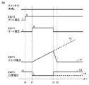
- FIG. 2 is a timing chart for explaining the operation of the test apparatus 110 and the test body 100 in the short-circuit test according to the first embodiment.
- FIG. 2 shows waveforms of the switch 33, the gate voltage of the IGBT 2, the gate voltage of the IGBT 1, the emitter current of the IGBT 1, and the collector-emitter (CE) voltage of the IGBT 1 in this order from the top.
- the switch 33 is also turned off by receiving the L level control signal and turned on by receiving the H level control signal.
- the control unit 31 inputs an H level control signal to the gate electrode of the IGBT 2 through the control unit 21 with the switch 33 held off. As a result, the IGBT 2 is turned on. At this time, since the L level control signal is input to the gate electrode of the IGBT 1, the IGBT 1 is not turned on. Therefore, no current flows between the high-voltage side main electrode 51 and the low-voltage side main electrode 52. In the test device 110, since the switch 33 is turned off, the capacitor 32 is not charged either. Therefore, after the time t0, only the capacitor 22 of the test body 100 is charged.
- the control unit 31 turns on the IGBT 1 by inputting an H level control signal to the gate electrode of the IGBT 1 through the control unit 21.
- the main electrodes 51 and 52 are short-circuited.
- a short-circuit current starts to flow between the main electrodes 51 and 52 due to the electric charge stored in the capacitor 22.
- the short-circuit current flows from the positive electrode of the capacitor 22 to the negative electrode of the capacitor 22 via the IGBT 1 and the IGBT 2 through the current path 61 shown by the solid line in FIG.
- the short-circuit current passes through the current path 62 shown by the broken line in FIG.
- the waveform of the emitter current of the IGBT 1 in FIG. 2 represents the temporal change of the short-circuit current.
- the short-circuit current flowing through the current path 61 and the short-circuit current flowing through the current path 62 are compared, the short-circuit current flowing through the current path 61 is much larger. Therefore, the short-circuit current flowing through the current path 62 can be ignored. This is because, in a general test apparatus, the maximum output current of the DC power supply 30 is often 1 A or less, so that most of the short-circuit current reaching several thousand A at time t2 is supplied from the capacitor 22. Further, the capacitor 22 is built in the same test body 100 as the IGBT 1, while the DC power supply 30 is often installed several meters away from the test body 100.
- the current path 62 contains a large stray inductance as compared with the current path 61, the stray inductance hinders the increase in the current. As a result, a current smaller than the maximum output current of the DC power supply 30 may flow in the current path 62.
- the emitter current (that is, short-circuit current) of the IGBT 1 increases after the time t1.
- the control unit 21 monitors the emitter current of the IGBT 1 based on the sense currents of the IGBT 1 and the IGBT 2. When a sense current equal to or higher than the threshold value is detected at time t2, the control unit 21 shifts the control signal input to the gate electrode of the IGBT 1 from the H level to the L level. As a result, the IGBT 1 is turned off.
- the short mode between the main electrodes 51 and 52 is canceled, so that the emitter current of the IGBT 1 sharply decreases after the time t2 as shown in the waveform k1.
- the collector-emitter voltage of the IGBT 1 increases to the H level as shown in the waveform k3.
- the IGBT 1 is destroyed during the short mode, the IGBT 1 is not turned off at the time t2, so that the emitter current continues to increase even after the time t2 as shown in the waveform k2.
- the collector-emitter voltage of the IGBT 1 is maintained at the L level as shown in the waveform k4.
- the applied voltage between the main electrodes 51 and 52 is 650 V
- the capacitance of the capacitor 22 is 1000 ⁇ F
- the resistance component contained in the current path 61 is 0.2 ⁇
- a short-circuit current of a maximum of 3250 A continues to flow for 2 msec. It will be.
- the capacitance of the capacitor 22 is set to the optimum capacitance according to the specifications of the test body 100, whereas the test device 110 needs to test various semiconductor elements, so that the capacitance of the capacitor 32 is It may be set to 10 times or more the capacitance of the capacitor 22.
- the contact area between the probe and the main electrode is smaller than the total area of the main electrode, so the rated current of the probe is often several tens of amperes. Therefore, as described above, the probes 41 and 42 are burnt out due to the continuous flow of a maximum current of 3250 A, or the probe 41 and the high-voltage side main electrode 51 and / or the probe 42 and the low-voltage side main electrode 52 are fused. There is a risk of As a result, every time the IGBT of the subject is destroyed, the operation of the test device 110 is stopped, and operations such as replacement of the probes 41 and 42 and / or failure confirmation of the test device 110 are required.
- the semiconductor test method according to the first embodiment when the IGBT 1 as a subject is destroyed, a short-circuit current is short-circuited in the current path 61 formed between the capacitor 22 and the IGBTs 1 and 2 inside the test body 100. Therefore, it is possible to prevent a large current from flowing through the test apparatus 110. Therefore, the progress of damage to the test jigs such as probes 41 and 42 in contact with the broken semiconductor element, the damage to the test body 100 caused by the damage to the test jig, and the damage to the test body 100 next to the test body 100. It is possible to suppress poor transportation of the test piece to be tested.
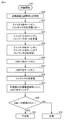
- FIG. 3 is a flowchart for explaining the processing procedure of the semiconductor test method according to the first embodiment.
- FIG. 3 illustrates a processing procedure for a short-circuit test when IGBT1 is used as a subject.
- step S01 when the short-circuit test by the test device 110 is started in step S01, the probes 41 and 42 of the test device 110 are connected to the main electrodes 51 and 52 of the test body 100, respectively, in step S02. As a result, the test body 100 and the test device 110 are electrically connected. Further, by connecting the probe 43 of the test device 110 to the control terminal 53 of the test body 100, the control unit 21 and the control unit 31 are communicably connected. In this state, in step S03, the control unit 31 does not charge the capacitor 32 by holding the switch 33 in the off state.
- step S04 the control unit 21 turns on the IGBT 2 by inputting an H level control signal to the gate electrode of the IGBT 2 in response to a command from the control unit 31.
- step S05 the control unit 31 applies a DC voltage from the DC power supply 30 of the test device 110 to the main electrodes 51 and 52 via the probes 41 and 42. By applying this DC voltage, the capacitor 22 inside the test piece 100 is charged in step S06.
- step S07 the control unit 21 turns on the IGBT 1 by inputting an H level control signal to the gate electrode of the IGBT 1.
- the IGBTs 1 and 2 are turned on, and the main electrodes 51 and 52 are short-circuited.
- the control unit 21 monitors the emitter current of the IGBT 1 based on the sense current of the IGBT 1 and the IGBT 2. When the sense current exceeds the threshold value, the control unit 21 detects the overcurrent of the emitter current of the IGBT 1. In this case, the control unit 21 turns off the IGBT 1 by shifting the control signal input to the gate electrode of the IGBT 1 from the H level to the L level in step S08.
- the control unit 21 determines that the IGBT 1 has been destroyed (YES in S09), and in step S10, the IGBT 1 Judges that the dynamic characteristics of are unacceptable.
- the control unit 21 determines that the IGBT 1 is not destroyed (NO in S09), and in step S11, the dynamic characteristics of the IGBT 1. Is determined to pass.
- the IGBT 1 When performing a short-circuit test using the IGBT 2 as a subject, the IGBT 1 may be replaced with the IGBT 2 and the IGBT 2 may be replaced with the IGBT 1 in the above description. Further, when performing a short-circuit test on the IGBTs of other phases of the three-phase inverter circuit 150, the IGBT 1 may be replaced with the IGBT of the other phase, and the IGBT 2 may be replaced with the IGBT connected in series with the IGBT of the other phase. .. In this way, a short circuit test can be performed on all of the IGBTs 1 to 6 constituting the three-phase inverter circuit 150.
- the capacitor 22 connected between the main electrodes 51 and 52 inside the test body 100 is precharged and stored in the capacitor 22.
- FIG. 4 is a circuit diagram showing the configuration of the semiconductor test apparatus according to the second embodiment.
- the semiconductor test apparatus 110 according to the second embodiment includes a series circuit of the capacitor 32 and the switch 33 as compared with the semiconductor test apparatus 110 according to the first embodiment shown in FIG. The difference is that there is no such thing.
- the capacitor 32 is charged by turning off the switch 33 before applying the DC voltage between the DC power supply 30 and the main electrodes 51 and 52 of the test body 100. Is not performed.
- the test device 110 since the test device 110 does not have the series circuit of the capacitor 32 and the switch 33, the process of turning off the switch 33 becomes unnecessary.
- the operation of the semiconductor test apparatus 110 according to the second embodiment will be described with reference to FIGS. 5 and 6. Also in the second embodiment, as in the first embodiment, the semiconductor element to be the subject is set to the IGBT 1, and the short circuit test of the IGBT 1 is performed. The operation of the semiconductor test device 110 according to the second embodiment will be described only in that it differs from the operation of the semiconductor test device 110 according to the first embodiment described with reference to FIGS. 2 and 3.
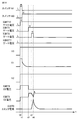
- FIG. 5 is a timing chart for explaining the operation of the test apparatus 110 and the test body 100 in the short circuit test according to the second embodiment.
- FIG. 5 shows waveforms of the gate voltage of the IGBT 2, the gate voltage of the IGBT 1, the emitter current of the IGBT 1, and the collector-emitter voltage of the IGBT 1 in this order from the top. That is, the timing chart of FIG. 5 is equivalent to the timing chart of FIG. 2 excluding the waveform of the switch 33.
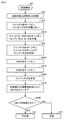
- FIG. 6 is a flowchart for explaining the processing procedure of the test method according to the second embodiment.
- the flowchart of FIG. 6 is equivalent to the flowchart shown in FIG. 3 excluding the process of step S03 (process of holding the switch 33 in the off state).
- the short circuit current is caused by the electric charge accumulated in the capacitor 22 due to the short circuit between the main electrodes 51 and 52. Begins to flow. Since most of the short-circuit current at this time flows through the current path 61 shown in FIG. 4, it is possible to prevent a large current from flowing through the test apparatus 110. Therefore, the same effects as those of the semiconductor test apparatus and test method according to the first embodiment can be obtained.
- FIG. 7 is a circuit diagram showing the configuration of the semiconductor test apparatus according to the third embodiment.
- the semiconductor test apparatus 110 according to the third embodiment has a different configuration of the test body 100 as compared with the semiconductor test apparatus 110 according to the first embodiment shown in FIG.
- the test body 100 according to the second configuration example shown in FIG. 7 includes an IGBT 1, a diode 11, and a capacitor 22.
- the emitter electrode of the IGBT 1 is connected to the high pressure side main electrode 51, and the collector electrode of the IGBT 1 is connected to the low pressure side main electrode 52.
- the diode 11 is connected to the IGBT 1 in antiparallel.
- the sense terminal (not shown) of the IGBT 1 is electrically connected to the control unit 21.
- the capacitor 22 is electrically connected in parallel with the IGBT 1 between the high voltage side main electrode 51 and the low voltage side main electrode 52.
- the short-circuit test of the object object IGBT1 can be executed according to the flowchart shown in FIG.
- the process of step S04 can be omitted. That is, while the test apparatus 110 is connected between the main electrodes 51 and 52 of the test body 100 (S01 in FIG. 3) and the switch 33 is held in the off state (S03 in FIG. 3), direct current is applied between the main electrodes 51 and 52. A voltage is applied (S05 in FIG. 3). When the capacitor 22 is charged in response to this DC voltage (S06 in FIG. 3), the control unit 21 turns on the IGBT 1 (S07 in FIG.
- the control unit 21 turns off the IGBT 1 (S08 in FIG. 3) and determines whether or not the IGBT 1 is destroyed based on the sense current after the turn-off (FIG. 3). S09).
- FIG. 8 is a circuit diagram showing the configuration of the semiconductor test apparatus according to the fourth embodiment.
- the semiconductor test apparatus 110 according to the fourth embodiment has a different structure of the test body as compared with the semiconductor test apparatus 110 according to the first embodiment shown in FIG.
- the test body 200 according to the third configuration example is a test body 100 according to the first configuration example shown in FIG. 1 in which a boost converter circuit 210 is added to the DC side of the three-phase inverter circuit 150.
- the boost converter circuit 210 includes semiconductor switching elements 7 and 8, diodes 17 and 18, a reactor 81, and input electrodes 91 and 92.
- each of the semiconductor switching elements 7 and 8 has a positive electrode, a negative electrode, and a control electrode, and controls on / off according to a control signal applied to the control electrode from the control unit 21. It is configured to be possible.
- the semiconductor switching elements 7 and 8 are IGBTs.
- the semiconductor switching elements 7 and 8 are also referred to as IGBTs 7 and 8.
- the input electrodes 91 and 92 correspond to one embodiment of the "first input electrode" and the "second input electrode".
- the emitter electrode of the IGBT 7 is connected to the high voltage side main electrode 51, and the emitter electrode of the IGBT 8 is connected to the low voltage side main electrode 52 and the low voltage side input electrode 92.
- the emitter electrode of the IGBT 7 and the collector electrode of the IGBT 8 are connected to the first terminal of the reactor 81.
- the second terminal of the reactor 81 is connected to the high voltage side input electrode 91.
- the test body 200 boosts the DC voltage applied between the input electrodes 91 and 92 to a voltage at which a load (for example, a motor) connected to the three-phase output electrode 25 can be driven by the boost converter circuit 210.
- the boosted voltage is converted into a three-phase AC voltage by the three-phase inverter circuit 150 and supplied to the load.
- the control unit 21 calculates a duty ratio for setting the output voltage of the boost converter circuit 210 to the target voltage, and turns on / off the IGBTs 7 and 8 of the boost converter circuit 210 based on the calculated duty ratio. Generate a control signal for control.
- the control unit 21 further generates a control signal for controlling the on / off of the IGBTs 1 to 6 of the three-phase inverter circuit 150.
- the control unit 21 inputs the generated control signal to the control electrodes of the IGBTs 1 to 8.
- the test apparatus 110 can perform a short-circuit test of the IGBTs 1 to 6 constituting the three-phase inverter circuit 150 by using the semiconductor test method according to the first embodiment.
- FIG. 9 is a circuit diagram showing the configuration of the semiconductor test apparatus according to the fifth embodiment.
- the semiconductor test apparatus 110 according to the fifth embodiment has a connection relationship of the test apparatus 110 to the test body 200 as compared with the semiconductor test apparatus 110 according to the fifth embodiment shown in FIG. different.
- the semiconductor test apparatus 110 is connected between the input electrodes 91 and 92 of the test body 200. Specifically, the probe 41 is connected to the high pressure side input electrode 91, and the probe 42 is connected to the low pressure side input electrode 92.
- FIG. 10 is a flowchart for explaining the processing procedure of the semiconductor test method according to the fifth embodiment.
- FIG. 10 illustrates a processing procedure for a short-circuit test when IGBT1 is used as a subject.
- step S051 the control unit 21 boosts the DC voltage applied between the input electrodes 91 and 92 to a target voltage (for example, 650V) by controlling the on / off of the IGBTs 7 and 8 constituting the boost converter circuit 210.
- a DC voltage for testing for example, 650V is generated between the main electrodes 51 and 52.
- step S06 the capacitor 22 inside the test piece 200 is charged by receiving the DC voltage generated between the main electrodes 51 and 52.
- the control unit 21 turns on the IGBT 1 (S07) and detects the short-circuit current based on the sense current of the IGBT 1.
- the control unit 21 turns off the IGBT 1 (S08) and determines whether or not the IGBT 1 is destroyed based on the sense current after the turn-off (S08).
- the avalanche test of the test body 200 can be performed.
- the avalanche test is the avalanche destruction caused by the energy stored in the reactor flowing at once between the positive and negative electrodes at the moment when the control signal input to the control electrode of the semiconductor switching element is changed from the H level to the L level. This is a test for evaluating resistance to.
- FIG. 11 illustrates the processing procedure of the avalanche test when IGBT1 is used as a subject.
- step S03 when the avalanche test by the test apparatus 110 is started in the same steps S01 to S03 as in FIG. 3, the probes 41 and 42 of the test apparatus 110 are attached to the main electrodes 51 and 52 of the test body 100, respectively. By connecting, the test body 100 and the test device 110 are electrically connected. In this state, in step S03, the capacitor 32 is not charged by holding the switch 33 in the off state.
- step S041 the control unit 21 turns on the IGBT 1 and the IGBT 2 by inputting an H level control signal to the respective gate electrodes of the IGBT 1 and the IGBT 2.
- the control unit 21 boosts the DC voltage applied between the input electrodes 91 and 92 by controlling the on / off of the IGBTs 7 and 8 constituting the boost converter circuit 210 in step S051, and between the main electrodes 51 and 52. Generate a test voltage (eg 650V).
- step S06 the capacitor 22 inside the test piece 200 is charged by receiving the DC voltage generated between the main electrodes 51 and 52. Further, in step S061, energy is stored in the reactor 81.
- the control unit 21 turns off the IGBT 1 by inputting an L level control signal to the gate electrode of the IGBT 1 in step S071.
- the collector-emitter voltage of the IGBT 1 rises to the avalanche voltage of the IGBT due to the energy stored in the reactor 81.
- the IGBT 1 enters the avalanche mode.
- the energy stored in the reactor 81 is consumed by the IGBT 1, so that the emitter current of the IGBT 1 decreases. If the avalanche destruction does not occur in the IGBT 1, the avalanche mode continues until all the energy stored in the reactor 81 is released, and the avalanche mode ends when the emitter current becomes 0.
- the collector-emitter voltage of the IGBT 1 decreases to near 0V. Therefore, the reactor 81 starts to store magnetic energy again, and the emitter current of the IGBT 1 starts to rise.
- the control unit 21 monitors the emitter current of the IGBT 1 for a reference time based on the sense current of the IGBT 1 in step S09.
- the reference time can be set based on the result of dividing the inductance value of the reactor 81 by the difference between the avalanche voltage of the IGBT 1 and the power supply voltage.
- the control unit 21 determines in step S10 that the dynamic characteristics of the IGBT 1 have failed. do.
- the control unit 21 determines that the avalanche destruction of the IGBT 1 has not occurred (NO in S09), and determines that the dynamic characteristics of the IGBT 1 have passed in step S11. do.
- the capacitor 22 connected between the main electrodes 51 and 52 is charged inside the test body 200, and the energy stored in the capacitor 22 is charged.
- FIG. 12 is a circuit diagram showing the configuration of the semiconductor test apparatus according to the sixth embodiment.
- the semiconductor test apparatus 110 according to the sixth embodiment has a different structure of the test body as compared with the semiconductor test apparatus 110 according to the first embodiment shown in FIG.
- the test body 200 includes a boost converter circuit 210, switches 160 and 161, discharge resistors 163, and input electrodes 91 and 92.
- a test device 110 is connected between the input electrodes 91 and 92.
- the power supply voltage VD of the DC power supply 30 included in the test device 110 is, for example, about 500V.
- the boost converter circuit 210 is called a multi-level chopper.
- the boost converter circuit 210 includes semiconductor switching elements 7 to 10, diodes 17 to 20, a reactor 81, and capacitors 24 and 25.
- each of the semiconductor switching elements 7 to 10 has a positive electrode, a negative electrode, and a control electrode, and controls on / off according to a control signal applied to the control electrode from the control unit 21. It is configured to be possible.
- the semiconductor switching elements 7 to 10 are IGBTs. In the following description, the semiconductor switching elements 7 to 10 are also referred to as IGBTs 7 to 10.
- the IGBTs 7 to 10 are connected in series between the high voltage side main electrode 51 and the low voltage side main electrode 52.
- the collector electrode of the IGBT 7 is connected to the high voltage side main electrode 51.
- the emitter electrode of the IGBT 8 and the collector electrode of the IGBT 9 are connected to the first terminal of the reactor 81.
- the second terminal of the reactor 81 is connected to the high voltage side input electrode 91.
- the emitter electrode of the IGBT 10 is connected to the low pressure side main electrode 52 and the low pressure side input electrode 92.
- the IGBTs 7 to 10 correspond to one embodiment of the "first semiconductor element", the "second semiconductor element", the "third semiconductor element", and the "fourth semiconductor element", respectively.
- the first terminal of the capacitor 24 is connected to the second terminal of the reactor 81 and the high voltage side input electrode 91, and the second terminal is connected to the low voltage side input electrode 92.
- the capacitor 24 is a smoothing capacitor for reducing voltage fluctuations between the input electrodes 91 and 92.
- the first terminal of the capacitor 25 is connected to the emitter electrode of the IGBT 7 and the collector electrode of the IGBT 8, and the second terminal is connected to the emitter electrode of the IGBT 9 and the collector electrode of the IGBT 10.
- the capacitor 25 is a charge pump configured to superimpose a voltage on an input voltage and boost the voltage by transitioning the stored electric charge.
- the capacitor 25 corresponds to one embodiment of the "third capacitor”.
- the first terminal of the switch 161 is connected to the high voltage side input electrode 91, and the second terminal is connected to the second terminal of the reactor 81.
- the switch 161 corresponds to an embodiment of the "second switch”.
- the switch 160 and the discharge resistor 163 are connected in series between the second terminal of the switch 161 and the low voltage side input electrode 92.
- the test body 200 boosts the DC voltage applied between the input electrodes 91 and 92 to a voltage at which the load connected between the main electrodes 51 and 52 can be driven by the boost converter circuit 210.
- Is configured to supply the load.
- the control unit 21 calculates a duty ratio for setting the output voltage of the boost converter circuit 210 to the target voltage, and turns on / off the IGBTs 7 to 10 of the boost converter circuit 210 based on the calculated duty ratio. Generate a control signal for control.
- the control unit 21 inputs the generated control signal to the control electrodes of the IGBTs 7 to 10.
- FIG. 13 is a timing chart for explaining the operation of the test apparatus 110 and the test body 200 in the short-circuit test according to the sixth embodiment.
- the switch 161 and the switch 160 the gate voltage of the IGBT 10, the gate voltage of the IGBT 7, the terminal voltage V0 of the capacitor 25, the terminal voltage V1 of the capacitor 24, the terminal voltage V2 of the capacitor 22, and the IGBT 10
- the waveforms of the collector-emitter (CE-to-CE) voltage, the CE-to-CE voltage of the IGBT 7, and the emitter current of the IGBT 7 are shown.
- the switches 161, 160 are also turned off by receiving the L level control signal and turned on by receiving the H level control signal, similarly to the IGBT.
- FIG. 14 is a flowchart for explaining the processing procedure of the short-circuit test when the IGBT 7 is used as the subject.
- the semiconductor test method according to the sixth embodiment will be described with reference to FIGS. 13 and 14.
- step S21 when the short-circuit test by the test device 110 is started in step S21, the probes 41 and 42 of the test device 110 are connected to the input electrodes 91 and 92 of the test body 200, respectively, in step S22.
- the test body 200 and the test device 110 are electrically connected to each other.
- the control unit 21 and the control unit 31 are communicably connected. In this state, in step S23, the control unit 31 does not charge the capacitor 32 by holding the switch 33 in the off state.
- step S24 the control unit 21 receives a command from the control unit 31 and inputs an H level control signal to the switch 161 to turn on the switch 161 (time t0 in FIG. 13).
- the control unit 21 turns off the switch 161 and turns on the switch 160 in step S25 (time t1 in FIG. 13). By turning off the switch 161 the test body 200 and the test device 110 are electrically cut off. When the switch 160 is turned on in this state, the discharge of the capacitor 24 is started. On the other hand, the diode 17 does not discharge the capacitor 22.
- step S26 the control unit 21 turns on the IGBT 10 by inputting an H level control signal to the gate electrode of the IGBT 10 in response to a command from the control unit 31 (time t2 in FIG. 13).
- the voltage between CEs of the IGBT 7 DC voltage VD.
- the control unit 21 receives a command from the control unit 31 and inputs an H level control signal to the gate electrode of the IGBT 7 to turn on the IGBT 7 (time in FIG. 13). t3).
- step S28 When both the IGBTs 7 and 10 are turned on and the main electrodes 51 and 52 are short-circuited (short-circuited), the discharge of the capacitor 22 is started in step S28.
- a short-circuit current begins to flow between the main electrodes 51 and 52 due to the electric charge stored in the capacitor 22.
- the short-circuit current flows from the positive electrode of the capacitor 22 to the negative electrode of the capacitor 22 via the IGBT 7, the capacitor 25 and the IGBT 10 through the current path 160 shown by the solid line in FIG.
- the control unit 21 monitors the emitter current of the IGBT 7 based on the sense current of the IGBT 7. When the sense current exceeds the threshold value, the control unit 21 detects the overcurrent of the IGBT 7. In this case, the control unit 21 turns off the IGBT 7 by shifting the control signal input to the gate electrode of the IGBT 7 from the H level to the L level in step S29 (time t4 in FIG. 13).
- the control unit 21 determines that the IGBT 7 has been destroyed (YES in S30), and in step S31, the IGBT 7 Judges that the dynamic characteristics of are unacceptable.
- the control unit 21 determines that the IGBT 7 has not been destroyed (NO in S30), and in step S32, the dynamic characteristics of the IGBT 7. Is determined to pass.
- the IGBT 7 When performing a short-circuit test using the IGBT 10 as a subject, the IGBT 7 may be replaced with the IGBT 10 and the IGBT 10 may be replaced with the IGBT 7 in the above description. However, if the capacitor 24 is not discharged at the time t1 of FIG. 13, the capacitor 25 will be charged at the time t2, so that the short-circuit test cannot be performed.
- FIG. 15 is a timing chart for explaining the operation of the test apparatus 110 and the test body 200 in the short circuit test according to the sixth embodiment.
- the switch 161 and the switch 160 in order from the top, the switch 161 and the switch 160, the gate voltage of the IGBT 10, the gate voltage of the IGBT 9, the gate voltage of the IGBT 8, the gate voltage of the IGBT 7, the terminal voltage V0 of the capacitor 25, and the terminal voltage V1 of the capacitor 24, The waveforms of the terminal voltage V2 of the capacitor 22, the CE voltage of the IGBT 9, the CE voltage of the IGBT 8, and the emitter current of the IGBT 8 are shown.
- the switches 161, 160 are also turned off by receiving the L level control signal and turned on by receiving the H level control signal, similarly to the IGBT.
- FIG. 16 is a flowchart for explaining the processing procedure of the short-circuit test when the IGBT 8 is used as the subject.
- the semiconductor test method according to the sixth embodiment will be described with reference to FIGS. 15 and 16.
- step S21 when the short-circuit test by the test device 110 is started in step S21, the probes 41 and 42 of the test device 110 are connected to the input electrodes 91 and 92 of the test body 200, respectively, in step S22.
- the test body 200 and the test device 110 are electrically connected to each other.
- the control unit 21 and the control unit 31 are communicably connected. In this state, in step S23, the control unit 31 does not charge the capacitor 32 by holding the switch 33 in the off state.
- step S240 the control unit 21 turns on the switch 161 by inputting an H level control signal to the switch 161 in response to a command from the control unit 31. Further, the control unit 21 turns on the IGBT 10 by inputting an H level control signal to the gate electrode of the IGBT 10 in response to a command from the control unit 31 (time t0 in FIG. 15).
- the control unit 21 turns off the switch 161 and turns on the switch 160 in step S25 (time t1 in FIG. 15).
- the switch 160 is turned on instead of the switch 161, the discharge of the capacitor 24 is started.
- the diode 17 does not discharge the capacitor 22. Further, the diode 18 does not discharge the capacitor 25.
- step S260 the control unit 21 turns on the IGBT 9 by inputting an H level control signal to the gate electrode of the IGBT 9 in response to a command from the control unit 31 (time t2 in FIG. 15).
- the voltage between CEs of the IGBT 8 DC voltage VD.
- step S270 the control unit 21 turns on the IGBT 8 by inputting an H level control signal to the gate electrode of the IGBT 8 in response to a command from the control unit 31 (time in FIG. 15). t3).
- step S28 When both the IGBTs 8 and 9 are turned on and the terminals of the capacitor 25 are short-circuited, the discharge of the capacitor 25 is started in step S28.
- a short-circuit current begins to flow in the IGBTs 8 and 9 due to the electric charge stored in the capacitor 25.
- the short-circuit current flows from the positive electrode of the capacitor 25 to the negative electrode of the capacitor 25 via the IGBT 8 and the IGBT 9 through the current path 161 shown by the broken line in FIG.
- the control unit 21 monitors the emitter current of the IGBT 8 based on the sense current of the IGBT 8. When the sense current exceeds the threshold value, the control unit 21 detects the overcurrent of the IGBT 8. In this case, the control unit 21 turns off the IGBT 8 by shifting the control signal input to the gate electrode of the IGBT 8 from the H level to the L level in step S290 (time t4 in FIG. 15).
- the control unit 21 determines that the IGBT 8 has been destroyed (YES in S300), and in step S31, the IGBT 8 Judges that the dynamic characteristics of are unacceptable.
- the control unit 21 determines that the IGBT 8 has not been destroyed (NO in S300), and in step S32, the dynamic characteristics of the IGBT 8 Is determined to pass.
- the IGBT 8 When performing a short-circuit test using the IGBT 9 as a subject, the IGBT 8 may be replaced with the IGBT 9 and the IGBT 9 may be replaced with the IGBT 8 in the above description.
- a multi-level chopper including IGBTs 7 to 10 connected in series between the main electrodes 51 and 52 and a capacitor 25 for a charge pump.
- the capacitor 22 connected between the main electrodes 51 and 52 is charged inside the test body 200 having the above, and the energy stored in the capacitor 22 is used to execute the test of the IGBT 7 or the IGBT 10.
- a short-circuit failure occurs, it is possible to prevent a large current from flowing through the test apparatus.
- the control unit 31 can be configured by using the function generator 310 and the pulse generator 312 as shown in FIG.
- the function generator 310 generates a signal voltage having a desired waveform and / or a desired frequency.
- the pulse generator 312 generates a control signal for controlling the three-phase inverter circuit 150 (including the boost converter circuit 210) of the test piece 100 (or 200) based on the signal voltage generated by the function generator 310.
- the generated control signal is transmitted to the control unit 21.
- control unit 31 can have a processor 314, a memory 316, an input / output interface (I / F) 318, and a communication I / F 320. Each of these parts is communicably connected to each other via a bus (not shown).
- the processor 314 is typically an arithmetic processing unit such as a CPU (Central Processing Unit) or an MPU (Micro Processing Unit).
- the processor 314 controls the operation of each part of the test apparatus 110 by reading and executing the program stored in the memory 316.
- non-volatile memory such as memory 316, RAM (Random Access Memory), ROM (Read Only Memory) and flash memory.
- the memory 316 stores a program executed by the processor 314, data used by the processor 314, and the like.
- the input / output I / F 318 is an interface for exchanging various data between the processor 314 and the display unit 324 and the input unit 322.
- the display unit 324 is composed of a liquid crystal panel or the like capable of displaying an image.
- the input unit 322 receives the user's operation input to the test device 110.
- the input unit 322 is typically composed of a touch panel, a keyboard, a mouse, and the like.
- the communication I / F 320 is a communication interface for exchanging various data between the test device 110 and other devices including the test bodies 100 and 200, and is realized by an adapter or a connector.
- the communication method may be a wireless communication method using a wireless LAN (Local Area Network) or the like, or a wired communication method using USB (Universal Serial Bus) or the like.
- Embodiment 7 a method of manufacturing the semiconductor device that becomes the test bodies 100 and 200 in the above-described first to sixth embodiments will be described.
- the seventh embodiment describes a method for manufacturing a semiconductor device, which includes the semiconductor test methods according to the first to fifth embodiments in the manufacturing process.
- the semiconductor device manufactured by this manufacturing method has a semiconductor switching element, and includes a first configuration example (see FIG. 1), a second configuration example (see FIG. 7), a third configuration example (see FIG. 8), and a third configuration example (see FIG. 8).
- Specimens 100 and 200 of the fourth configuration example can be applied.
- the semiconductor device is the test body 100 (see FIG. 1) of the first configuration example. That is, the semiconductor device has a full-bridge type three-phase inverter circuit 150, a control unit 21, a capacitor 22, and a discharge resistor 23.
- FIG. 19 is a flowchart for explaining a method of manufacturing a semiconductor device according to the sixth embodiment.
- the semiconductor device manufacturing method includes a step of assembling the semiconductor device (S100), a step of testing the dynamic characteristics of the assembled semiconductor device (S200), and commercializing a semiconductor device that has passed the test. It includes a step (S300).
- the step of manufacturing the three-phase inverter circuit 150 (S110), the step of manufacturing the control unit 21 (S120), the manufactured three-phase inverter circuit 150, the control unit 21, the discharge resistor 23, and so on. It includes a step of mounting the capacitor 22 (S130) and a step of wiring between the mounted three-phase inverter circuit 150, the control unit 21, the discharge resistor 23, and the capacitor 22 (S140).
- semiconductor switching elements (IGBTs) 1 to 6 and diodes 11 to 16 are mounted on the substrate.
- control unit 21 In the step of manufacturing the control unit 21 (S120), a function generator (or microcomputer) constituting the control unit 21, a gate drive circuit of a semiconductor switching element, and the like are mounted on the substrate.
- the substrate on which the three-phase inverter circuit 150 is manufactured and the substrate on which the control unit 21 is manufactured are mounted on the housing of the semiconductor device.
- a discharge resistor 23 and a capacitor 22 are further mounted on the housing.
- the three-phase inverter circuit 150, the control unit 21, the discharge resistance 23, and the capacitor 22 are connected by wiring between the electrodes, the discharge resistance 23, and the capacitor 22 on the substrate mounted on the housing. Are electrically connected to each other. As a result, the semiconductor device (test body 100) shown in FIG. 1 is assembled.
- a test for confirming the functions of the individually manufactured three-phase inverter circuit 150, the control unit 21, and the like is carried out, and those that pass the test are mounted on the housing of the semiconductor device.
- the configuration is to be used.
- the three-phase inverter circuit 150 and the control unit 21 may not be manufactured individually, but these components may be manufactured directly in the housing of the semiconductor device.
- the work of testing each component can be omitted, so that the man-hours can be reduced, but the defect rate may be deteriorated. Therefore, it is sufficient to compare the increase in the cost rate due to the increase in man-hours with the increase in the cost rate due to the deterioration of the defective rate, and adopt a configuration in which the increase is small.
- a characteristic test is executed using the assembled semiconductor device as a test body.
- the characteristic test of the semiconductor device is performed according to the processing procedure described with reference to FIG. That is, when the semiconductor test device 110 (see FIG. 1) is electrically connected to the semiconductor device, a test (short-circuit test or the like) of the dynamic characteristics of the semiconductor switching element to be the subject is executed.
- step of commercializing first, it is determined whether the test result in the step of testing (S200) passes or fails (S310).
- a step (S320) of attaching the upper lid to the housing is performed on the semiconductor device whose test result is acceptable (YES in S310).
- the housing of the semiconductor device is sealed to become a product.
- the semiconductor device whose test result is unacceptable NO in S310
- the commercialized semiconductor device is shipped by the shipping process (S330).
- a capacitor connected between the main electrodes 51 and 52 inside the semiconductor device. 22 is charged in advance, and the characteristic test of the subject is executed using the energy stored in the capacitor 22. This makes it possible to prevent a large current from flowing through the semiconductor test apparatus when the subject is destroyed during the test. As a result, it is possible to suppress the progress of damage to the semiconductor test apparatus due to the breaking current of the semiconductor element.
- each embodiment can be combined, and each embodiment can be appropriately modified or omitted.
Abstract
In the present invention, a test body (100) comprises: a first semiconductor element (1); a first primary electrode (51) that is electrically connected to a positive electrode of the first semiconductor element (1); a second primary electrode (52) that is electrically connected to a negative electrode of the first semiconductor element (1); and a first capacitor (22) that is connected between the first primary electrode (51) and the second primary electrode (52). A semiconductor testing device (110) comprises: a direct current source (30) that is connected between a first probe (41) and a second probe (42); and a control unit (31). When the first probe (41) is connected to the first primary electrode (51) and the second probe (42) is connected to the second primary electrode (52), the control unit (31) charges the first capacitor (22) with direct current voltage supplied from the direct current source (30), and after charging the first capacitor (22), inputs a control signal for turning ON the first semiconductor element (1) to a control electrode of the first semiconductor element (1).
Description
本開示は、半導体試験装置、半導体試験方法および半導体装置の製造方法に関する。
The present disclosure relates to a semiconductor test device, a semiconductor test method, and a method for manufacturing a semiconductor device.
半導体素子の製品性能は、製造過程における試験工程において特性試験(高電圧および/または高電流を半導体素子に与えるなどの特性検査およびスクリーニングなど)が行なわれることによって、保証されている。一方、このような特性試験の課題として、半導体素子が破壊されたときに大きな破壊電流が半導体素子および半導体試験装置間を流れることにより、半導体素子および半導体試験装置に損傷を与えてしまうという問題がある。
The product performance of semiconductor devices is guaranteed by performing characteristic tests (characteristic inspection and screening such as applying high voltage and / or high current to semiconductor devices) in the test process in the manufacturing process. On the other hand, as a problem of such a characteristic test, there is a problem that when a semiconductor element is destroyed, a large breakdown current flows between the semiconductor element and the semiconductor test device, thereby damaging the semiconductor element and the semiconductor test device. be.
特開2014-175643号公報(特許文献1)には、半導体トランジスタのテスト方法として、試験電圧印加回路に内蔵されるキャパシタの一端を試験電圧に充電する工程と、充電された上記キャパシタの一端を被試験トランジスタのドレイン端子に接続することにより、ドレイン端子に試験電圧を印加する工程とを備える構成が開示されている。
Japanese Patent Application Laid-Open No. 2014-175643 (Patent Document 1) describes, as a method for testing a semiconductor transistor, a step of charging one end of a capacitor built in a test voltage application circuit to a test voltage, and one end of the charged capacitor. A configuration including a step of applying a test voltage to the drain terminal by connecting to the drain terminal of the transistor under test is disclosed.
特許文献1では、予め充電されたキャパシタを介して被試験トランジスタのドレイン端子に試験電圧を印加することにより、高電圧試験中に被試験トランジスタに不良が発生した場合に、試験装置側から被試験トランジスタに流れ込む電荷量を最小限に抑制することができる。これにより、不良発生箇所から破壊ダメージが拡大することを防止できるため、不良の原因となって因子および不良発生箇所の特定が容易となる。
In Patent Document 1, by applying a test voltage to the drain terminal of the transistor under test via a pre-charged capacitor, when a defect occurs in the transistor under test during a high voltage test, the test apparatus side takes the test. The amount of charge flowing into the transistor can be minimized. As a result, it is possible to prevent the destruction damage from spreading from the defect occurrence location, so that it becomes easy to identify the factor and the defect occurrence location that cause the defect.
しかしながら、特許文献1に記載される試験方法では、試験装置がコンデンサを備えているため、大きな電荷量を必要とする短絡試験などの動特性試験中に、被検体である半導体素子が破壊した場合に、少なからず試験治具などの試験装置の損傷が進行してしまうおそれがある。その結果、試験装置の修理または交換が必要になるなどの問題が生じ得る。
However, in the test method described in Patent Document 1, since the test apparatus is provided with a capacitor, when the semiconductor element as a subject is destroyed during a dynamic characteristic test such as a short circuit test that requires a large amount of charge. In addition, there is a risk that damage to test equipment such as test jigs will progress. As a result, problems such as the need to repair or replace the test equipment may occur.
本開示は上記のような課題を解決するためになされたものであって、本開示の目的は、半導体素子の破壊電流による試験装置の損傷の進行を抑えることができる半導体試験装置および半導体試験方法ならびに当該半導体素子を有する半導体装置の製造方法を提供することである。
The present disclosure has been made to solve the above-mentioned problems, and an object of the present disclosure is a semiconductor test apparatus and a semiconductor test method capable of suppressing the progress of damage to the test apparatus due to a breaking current of a semiconductor element. Another object of the present invention is to provide a method for manufacturing a semiconductor device having the semiconductor element.
本開示のある局面では、半導体試験装置は、第1半導体素子を有する試験体の特性を試験するための半導体試験装置である。第1半導体素子は、正極、負極および制御電極を有しており、制御電極に入力される第1制御信号に応じてオンまたはオフされる。試験体は、第1半導体素子の正極と電気的に接続される第1主電極と、第1半導体素子の負極と電気的に接続される第2主電極と、第1主電極および第2主電極の間に電気的に接続される第1コンデンサとをさらに有する。半導体試験装置は、第1プローブおよび第2プローブと、第1プローブおよび第2プローブの間に電気的に接続される直流電源と、第1制御信号を生成するための制御部とを備える。第1プローブが第1主電極に接続され、かつ、第2プローブが第2主電極に接続されたとき、制御部は、直流電源から供給される直流電圧により第1コンデンサを充電し、かつ、第1コンデンサを充電した後に、第1半導体素子をオンするための第1制御信号を第1半導体素子の制御電極に入力する。
In a certain aspect of the present disclosure, the semiconductor test apparatus is a semiconductor test apparatus for testing the characteristics of a test piece having a first semiconductor element. The first semiconductor element has a positive electrode, a negative electrode, and a control electrode, and is turned on or off according to a first control signal input to the control electrode. The test piece includes a first main electrode electrically connected to the positive electrode of the first semiconductor element, a second main electrode electrically connected to the negative electrode of the first semiconductor element, a first main electrode, and a second main electrode. It further has a first capacitor that is electrically connected between the electrodes. The semiconductor test apparatus includes a first probe and a second probe, a DC power supply electrically connected between the first probe and the second probe, and a control unit for generating a first control signal. When the first probe is connected to the first main electrode and the second probe is connected to the second main electrode, the control unit charges the first capacitor with the DC voltage supplied from the DC power supply and charges the first capacitor. After charging the first capacitor, a first control signal for turning on the first semiconductor element is input to the control electrode of the first semiconductor element.
本開示の別の局面では、半導体試験方法は、半導体素子を有する試験体の特性を試験するための半導体試験方法である。半導体体素子は、正極、負極および制御電極を有しており、制御電極に入力される制御信号に応じてオンまたはオフされる。試験体は、半導体素子の正極と電気的に接続される第1主電極と、半導体素子の負極と電気的に接続される第2主電極と、第1主電極および第2主電極の間に電気的に接続される第1コンデンサとをさらに有する。半導体試験方法は、第1主電極および第2主電極の間に電気的に接続された直流電源から供給される直流電圧により第1コンデンサを充電するステップと、第1コンデンサを充電した後に、半導体素子をオンするための制御信号を半導体素子の制御電極に入力するステップとを備える。
In another aspect of the present disclosure, the semiconductor test method is a semiconductor test method for testing the characteristics of a test body having a semiconductor element. The semiconductor body element has a positive electrode, a negative electrode, and a control electrode, and is turned on or off according to a control signal input to the control electrode. The test piece is located between the first main electrode electrically connected to the positive electrode of the semiconductor element, the second main electrode electrically connected to the negative electrode of the semiconductor element, and the first and second main electrodes. It further has a first capacitor that is electrically connected. The semiconductor test method consists of a step of charging the first capacitor with a DC voltage supplied from a DC power source electrically connected between the first main electrode and the second main electrode, and a semiconductor after charging the first capacitor. It includes a step of inputting a control signal for turning on the element to the control electrode of the semiconductor element.
本開示の別の局面では、半導体装置の製造方法は、半導体素子を筐体に実装することにより半導体装置を組み立てる工程と、半導体装置の特性を試験する工程と、試験する工程において合格した半導体装置を製品化する工程とを備える。半導体素子は、正極、負極および制御電極を有しており、制御電極に入力される制御信号に応じてオンまたはオフされる。半導体装置は、半導体素子の正極と電気的に接続される第1主電極と、半導体素子の負極と電気的に接続される第2主電極と、第1主電極および第2主電極の間に電気的に接続される第1コンデンサとをさらに有する。試験する工程は、第1主電極および第2主電極の間に電気的に接続された直流電源から供給される直流電圧により前記第1コンデンサを充電するステップと、第1コンデンサを充電した後に、半導体素子をオンするための制御信号を前記半導体素子の制御電極に入力するステップとを備える。
In another aspect of the present disclosure, the method for manufacturing a semiconductor device is a process of assembling the semiconductor device by mounting the semiconductor element in a housing, a step of testing the characteristics of the semiconductor device, and a step of testing the semiconductor device. It is equipped with a process for commercializing. The semiconductor element has a positive electrode, a negative electrode, and a control electrode, and is turned on or off according to a control signal input to the control electrode. The semiconductor device is located between the first main electrode electrically connected to the positive electrode of the semiconductor element, the second main electrode electrically connected to the negative electrode of the semiconductor element, and the first and second main electrodes. It further has a first capacitor that is electrically connected. The steps to be tested include a step of charging the first capacitor with a DC voltage supplied from a DC power source electrically connected between the first and second main electrodes, and after charging the first capacitor. It includes a step of inputting a control signal for turning on the semiconductor element to the control electrode of the semiconductor element.
本開示によれば、半導体素子の破壊電流による試験装置の損傷の進行を抑えることができる半導体試験装置および半導体試験方法ならびに半導体装置の製造方法を提供することができる。
According to the present disclosure, it is possible to provide a semiconductor test device, a semiconductor test method, and a method for manufacturing a semiconductor device, which can suppress the progress of damage to the test device due to a breaking current of a semiconductor element.
以下、本開示の実施の形態について、図面を参照して詳細に説明する。なお、以下では、図中の同一または相当部分には同一符号を付して、その説明は原則的に繰返さないものとする。
Hereinafter, embodiments of the present disclosure will be described in detail with reference to the drawings. In the following, the same or corresponding parts in the drawings are designated by the same reference numerals, and the explanations will not be repeated in principle.
実施の形態1.
(半導体試験装置の構成)
図1は、実施の形態1に係る半導体試験装置の構成を示す回路図である。実施の形態1に係る半導体試験装置110は、被検体である半導体スイッチング素子を有する試験体100の短絡試験などの動特性を試験するための装置である。以下の説明では、半導体試験装置110を単に「試験装置110」とも称する。Embodiment 1.
(Semiconductor test equipment configuration)
FIG. 1 is a circuit diagram showing a configuration of a semiconductor test apparatus according to the first embodiment. Thesemiconductor test apparatus 110 according to the first embodiment is an apparatus for testing dynamic characteristics such as a short-circuit test of a test body 100 having a semiconductor switching element as a subject. In the following description, the semiconductor test apparatus 110 is also simply referred to as "test apparatus 110".
(半導体試験装置の構成)
図1は、実施の形態1に係る半導体試験装置の構成を示す回路図である。実施の形態1に係る半導体試験装置110は、被検体である半導体スイッチング素子を有する試験体100の短絡試験などの動特性を試験するための装置である。以下の説明では、半導体試験装置110を単に「試験装置110」とも称する。
(Semiconductor test equipment configuration)
FIG. 1 is a circuit diagram showing a configuration of a semiconductor test apparatus according to the first embodiment. The
図1を参照して、試験装置110は、直流電源30と、制御部31と、コンデンサ32と、スイッチ33と、プローブ41,42,43とを備える。直流電源30は、試験体100の主電極51,52間に直流電圧を印加するように構成される。直流電源30は、例えば蓄電池である。直流電源30の電源電圧は例えば650V程度である。
With reference to FIG. 1, the test apparatus 110 includes a DC power supply 30, a control unit 31, a capacitor 32, a switch 33, and probes 41, 42, 43. The DC power supply 30 is configured to apply a DC voltage between the main electrodes 51 and 52 of the test piece 100. The DC power supply 30 is, for example, a storage battery. The power supply voltage of the DC power supply 30 is, for example, about 650V.
制御部31は、試験体100に含まれる制御部21と電気的に接続され、被検体を試験するために制御部21を制御するように構成される。
The control unit 31 is electrically connected to the control unit 21 included in the test body 100, and is configured to control the control unit 21 for testing the subject.
コンデンサ32およびスイッチ33は、直流電源30の正極と負極との間に電気的に直列に接続される。コンデンサ32には、例えば、電解コンデンサ、フィルムコンデンサまたはセラミックコンデンサなどを用いることができる。コンデンサ32は、直流電源30の供給能力を超える電流を試験体100に短時間に供給する場合に有用である。また、コンデンサ32により、直流電源30の直流電圧の平滑化が可能となる。コンデンサ32は「第2コンデンサ」の一実施例に対応する。
The capacitor 32 and the switch 33 are electrically connected in series between the positive electrode and the negative electrode of the DC power supply 30. For the capacitor 32, for example, an electrolytic capacitor, a film capacitor, a ceramic capacitor, or the like can be used. The capacitor 32 is useful when supplying a current exceeding the supply capacity of the DC power supply 30 to the test piece 100 in a short time. Further, the capacitor 32 makes it possible to smooth the DC voltage of the DC power supply 30. The capacitor 32 corresponds to one embodiment of the "second capacitor".
スイッチ33は、直流電源30によるコンデンサ32の充電を遮断するための遮断回路を構成する。スイッチ33には、半導体スイッチまたは機械式スイッチを適用することができる。半導体スイッチは、代表的には、IGBTまたはMOSFETなどの半導体スイッチング素子である。機械式スイッチは、例えばリレーなどの開閉器である。スイッチ33は「第1スイッチ」の一実施例に対応する。
The switch 33 constitutes a cutoff circuit for cutting off the charging of the capacitor 32 by the DC power supply 30. A semiconductor switch or a mechanical switch can be applied to the switch 33. The semiconductor switch is typically a semiconductor switching element such as an IGBT or MOSFET. The mechanical switch is, for example, a switch such as a relay. The switch 33 corresponds to an embodiment of the "first switch".
スイッチ33は、制御部31から与えられる制御信号に従って、導通(オン)または非導通(オフ)される。スイッチ33をターンオンすることにより、直流電源30からコンデンサ32に直流電力が供給され、コンデンサ32が充電される。スイッチ33をターンオフすることにより、コンデンサ32の充電が遮断される。
The switch 33 is conducted (on) or non-conducted (off) according to the control signal given from the control unit 31. By turning on the switch 33, DC power is supplied from the DC power supply 30 to the capacitor 32, and the capacitor 32 is charged. By turning off the switch 33, the charging of the capacitor 32 is cut off.
プローブ41は、第1端子が直流電源30の正極と電気的に接続され、第2端子が試験体100の高圧側主電極51と電気的に接続される。プローブ42は、第1端子が直流電源30の負極と電気的に接続され、第2端子が試験体100の低圧側主電極52と電気的に接続される。プローブ43は、第1端子が制御部31と電気的に接続され、第2端子が試験体100の制御端子53と電気的に接続される。制御端子53は制御部21と電気的に接続されている。プローブ41は「第1プローブ」の一実施例に対応し、プローブ42は「第2プローブ」の一実施例に対応する。高圧側主電極51は「第1主電極」の一実施例に対応し、低圧側主電極52は「第2主電極」の一実施例に対応する。
In the probe 41, the first terminal is electrically connected to the positive electrode of the DC power supply 30, and the second terminal is electrically connected to the high voltage side main electrode 51 of the test piece 100. The first terminal of the probe 42 is electrically connected to the negative electrode of the DC power supply 30, and the second terminal is electrically connected to the low voltage side main electrode 52 of the test piece 100. In the probe 43, the first terminal is electrically connected to the control unit 31, and the second terminal is electrically connected to the control terminal 53 of the test piece 100. The control terminal 53 is electrically connected to the control unit 21. The probe 41 corresponds to an embodiment of the "first probe", and the probe 42 corresponds to an embodiment of the "second probe". The high-pressure side main electrode 51 corresponds to one embodiment of the “first main electrode”, and the low-pressure side main electrode 52 corresponds to one embodiment of the “second main electrode”.
(試験体100の第1構成例)
第1構成例に係る試験体100は、主回路として、高圧側主電極51と低圧側主電極52との間に入力される直流電力を三相交流電力に変換するフルブリッジ型の三相インバータ回路150と、三相出力電極25(U相出力電極25_1、V相出力電極25_2、W相出力電極25_3)と、三相インバータ回路150を制御するための制御部21と、コンデンサ22と、放電抵抗23とを備える。 (First configuration example of test body 100)
Thetest body 100 according to the first configuration example is a full-bridge type three-phase inverter that converts DC power input between the high-voltage side main electrode 51 and the low-voltage side main electrode 52 into three-phase AC power as a main circuit. The circuit 150, the three-phase output electrode 25 (U-phase output electrode 25_1, V-phase output electrode 25_2, W-phase output electrode 25_3), the control unit 21 for controlling the three-phase inverter circuit 150, the capacitor 22, and the discharge. It includes a resistor 23.
第1構成例に係る試験体100は、主回路として、高圧側主電極51と低圧側主電極52との間に入力される直流電力を三相交流電力に変換するフルブリッジ型の三相インバータ回路150と、三相出力電極25(U相出力電極25_1、V相出力電極25_2、W相出力電極25_3)と、三相インバータ回路150を制御するための制御部21と、コンデンサ22と、放電抵抗23とを備える。 (First configuration example of test body 100)
The
三相インバータ回路150は、半導体スイッチング素子1~6と、ダイオード11~16とを有する。半導体スイッチング素子1~6の各々は、正極、負極および制御電極を有する。半導体スイッチング素子1~6は、制御部21から制御電極に入力される制御信号(電圧または電流)に応じて、正極および負極間の電流経路の形成(オン)および遮断(オフ)を制御可能に構成される。
The three-phase inverter circuit 150 includes semiconductor switching elements 1 to 6 and diodes 11 to 16. Each of the semiconductor switching elements 1 to 6 has a positive electrode, a negative electrode, and a control electrode. The semiconductor switching elements 1 to 6 can control the formation (on) and cutoff (off) of the current path between the positive electrode and the negative electrode according to the control signal (voltage or current) input from the control unit 21 to the control electrode. It is composed.
半導体スイッチング素子1~6には、自己消弧型の任意の半導体素子を適用することができる。例えば、半導体スイッチング素子がMOSFET(Metal-Oxide-Semiconductor Field-Effect Transistor)である場合、正極はドレイン電極、負極はソース電極、制御電極はゲート電極を意味する。半導体スイッチング素子がIGBT(Insulated Gate Transistor)である場合には、正極はエミッタ電極、負極はコレクタ電極、制御電極はゲート電極を意味する。図1の構成例では、半導体スイッチング素子はIGBTである。以下の説明では、半導体スイッチング素子1~6を、IGBT1~6とも称する。
Any self-extinguishing semiconductor element can be applied to the semiconductor switching elements 1 to 6. For example, when the semiconductor switching element is a MOSFET (Metal-Oxide-Semiconductor Field-Effect Transistor), the positive electrode means a drain electrode, the negative electrode means a source electrode, and the control electrode means a gate electrode. When the semiconductor switching element is an IGBT (Insulated Gate Transistor), the positive electrode means an emitter electrode, the negative electrode means a collector electrode, and the control electrode means a gate electrode. In the configuration example of FIG. 1, the semiconductor switching element is an IGBT. In the following description, the semiconductor switching elements 1 to 6 are also referred to as IGBTs 1 to 6.
三相インバータ回路150において、IGBT1,3,5のエミッタ電極は高圧側主電極51と接続され、IGBT2,4,6のコレクタ電極は低圧側主電極52と接続される。IGBT1のコレクタ電極とIGBT2のエミッタ電極とは、U相出力電極25_1で接続される。IGBT3のコレクタ電極とIGBT4のエミッタ電極とは、V相出力電極25_2で接続される。IGBT5のコレクタ電極とIGBT6のエミッタ電極とは、W相出力電極25_3で接続される。三相出力電極25は、例えばモータなどの負荷に接続され、負荷を駆動するために用いられる。
In the three-phase inverter circuit 150, the emitter electrodes of the IGBTs 1, 3 and 5 are connected to the high-voltage side main electrodes 51, and the collector electrodes of the IGBTs 2, 4 and 6 are connected to the low-voltage side main electrodes 52. The collector electrode of the IGBT 1 and the emitter electrode of the IGBT 2 are connected by a U-phase output electrode 25_1. The collector electrode of the IGBT 3 and the emitter electrode of the IGBT 4 are connected by a V-phase output electrode 25_2. The collector electrode of the IGBT 5 and the emitter electrode of the IGBT 6 are connected by a W phase output electrode 25_3. The three-phase output electrode 25 is connected to a load such as a motor and is used to drive the load.
ダイオード11~16は、IGBT1~6にそれぞれ逆並列に接続され、還流ダイオードを構成する。半導体スイッチング素子にMOSFETを用いた場合には、内蔵されたボディダイオードを還流ダイオードとして用いることができる。半導体スイッチング素子を構成する材料としては、シリコン(Si)の他に、ワイドバンドギャップ半導体であるシリコンカーバイド(SiC)またはガリウムナイトライド(GaN)を適用することが可能である。
Diodes 11 to 16 are connected to IGBTs 1 to 6 in antiparallel, respectively, to form a freewheeling diode. When a MOSFET is used as a semiconductor switching element, the built-in body diode can be used as a freewheeling diode. As a material constituting the semiconductor switching element, in addition to silicon (Si), silicon carbide (SiC) or gallium nitride (GaN), which is a wide bandgap semiconductor, can be applied.
なお、図示は省略するが、IGBT1~6の各々のエミッタ電極にはセンス端子が接続されている。センス端子は制御部21と電気的に接続されている。センス端子には、対応するIGBTのコレクタ電極およびエミッタ電極間に流れる主電流(エミッタ電流)を一定比率(例えば1/10000など)で分流した電流(以下、センス電流とも称する)が流れる。
Although not shown, a sense terminal is connected to each emitter electrode of IGBTs 1 to 6. The sense terminal is electrically connected to the control unit 21. A current (hereinafter, also referred to as a sense current) obtained by dividing the main current (emitter current) flowing between the collector electrode and the emitter electrode of the corresponding IGBT at a constant ratio (for example, 1/10000) flows through the sense terminal.
制御部21は、IGBT1~6の各々のセンス電流に基づいて、試験体100の主電極51,52または三相出力電極25_1~25_3に流れる電流を制御するように構成される。例えば、IGBT1のセンス電流が閾値以上(例えば1A以上)となった場合、制御部21は、IGBT1の主電流(エミッタ電流)が過電流であると判定し、IGBT1をターンオフするための制御信号を生成する。制御部21は、生成した制御信号をIGBT1のゲート電極に入力する。
The control unit 21 is configured to control the current flowing through the main electrodes 51 and 52 or the three-phase output electrodes 25_1 to 25_3 of the test body 100 based on the respective sense currents of the IGBTs 1 to 6. For example, when the sense current of the IGBT 1 becomes equal to or higher than the threshold value (for example, 1A or higher), the control unit 21 determines that the main current (emitter current) of the IGBT 1 is an overcurrent, and outputs a control signal for turning off the IGBT 1. Generate. The control unit 21 inputs the generated control signal to the gate electrode of the IGBT 1.
IGBT1~6の各々は、ゲート電極に入力される制御信号がL(論理ロー)レベルからH(論理ハイ)レベルに遷移したときにターンオンされ、制御信号がHレベルからLレベルに遷移したときにターンオフされる。なお、IGBT1~6の各々を、制御信号がHレベルからLレベルに遷移したときにターンオンされ、制御信号がLレベルからHレベルに遷移したときにターンオフされる構成としてもよい。
Each of IGBTs 1 to 6 is turned on when the control signal input to the gate electrode transitions from the L (logical low) level to the H (logical high) level, and when the control signal transitions from the H level to the L level. Turn off. Each of the IGBTs 1 to 6 may be turned on when the control signal transitions from the H level to the L level, and may be turned off when the control signal transitions from the L level to the H level.
制御部21には、ファンクションジェネレータ(任意波形発生器)を用いることができる。あるいは、制御部21が有する機能を、マイクロコンピュータによるソフトウェア処理および/またはハードウェア処理によって実現することができる。
A function generator (arbitrary waveform generator) can be used for the control unit 21. Alternatively, the function of the control unit 21 can be realized by software processing and / or hardware processing by a microcomputer.
試験装置110を用いた試験体100の試験中、制御部31は、IGBT1~6をオンオフするための制御信号を生成する。制御部21は、プローブ43および制御端子53を介して、制御部31から制御信号を受信する。制御部21は、受信した制御信号をIGBT1~6のゲート電極に入力する。
During the test of the test body 100 using the test device 110, the control unit 31 generates a control signal for turning on / off the IGBTs 1 to 6. The control unit 21 receives a control signal from the control unit 31 via the probe 43 and the control terminal 53. The control unit 21 inputs the received control signal to the gate electrodes of the IGBTs 1 to 6.
コンデンサ22は、高圧側主電極51と低圧側主電極52との間に電気的に接続される。コンデンサ22は、直流電圧の平滑用コンデンサである。コンデンサ22は、例えば、電解コンデンサ、フィルムコンデンサまたはセラミックコンデンサなどを用いることができる。コンデンサ22は「第1コンデンサ」の一実施例に対応する。
The capacitor 22 is electrically connected between the high voltage side main electrode 51 and the low voltage side main electrode 52. The capacitor 22 is a DC voltage smoothing capacitor. As the capacitor 22, for example, an electrolytic capacitor, a film capacitor, a ceramic capacitor, or the like can be used. The capacitor 22 corresponds to one embodiment of the "first capacitor".
放電抵抗23は、コンデンサ22ならびに図示しない試験体100の配線およびIGBT1~6の浮遊容量を放電するための抵抗である。例えば、実稼働中に断線等の発生により、試験体100と試験体100を制御する外部制御回路とが電気的に遮断された場合、試験体100に充電された電荷を放電するために、放電抵抗23が用いられる。この場合、断線が発生してから数秒間内に放電が完了することが望ましい。例えば、コンデンサ22、試験体100の配線およびIGBT1~6の浮遊容量の総和が100μFであるとすると、放電抵抗23の抵抗値が20kΩ程度であることが望ましい。
The discharge resistor 23 is a resistor for discharging the wiring of the capacitor 22 and the test body 100 (not shown) and the stray capacitance of the IGBTs 1 to 6. For example, when the test body 100 and the external control circuit that controls the test body 100 are electrically cut off due to disconnection or the like during actual operation, the test body 100 is discharged in order to discharge the charged charge. The resistor 23 is used. In this case, it is desirable that the discharge be completed within a few seconds after the disconnection occurs. For example, assuming that the total stray capacitance of the capacitor 22, the wiring of the test body 100, and the stray capacitances of the IGBTs 1 to 6 is 100 μF, it is desirable that the resistance value of the discharge resistor 23 is about 20 kΩ.
(半導体試験装置の動作)
次に、実施の形態1に係る半導体試験装置110の動作について説明する。 (Operation of semiconductor test equipment)
Next, the operation of thesemiconductor test apparatus 110 according to the first embodiment will be described.
次に、実施の形態1に係る半導体試験装置110の動作について説明する。 (Operation of semiconductor test equipment)
Next, the operation of the
最初に、実施の形態1に係る半導体試験方法の比較例として、試験装置110を用いた一般的な半導体試験方法について説明する。
First, as a comparative example of the semiconductor test method according to the first embodiment, a general semiconductor test method using the test apparatus 110 will be described.
一般的な半導体試験方法では、試験装置110において、スイッチ33をオンさせることにより、直流電源30を用いてコンデンサ32を予め充電させておく。これにより、試験体100への給電は、充電されたコンデンサ32により行なわれる。なお、コスト削減のため、直流電源30には、最大出力電流が1A以下の高圧電源が用いられることが多い。
In a general semiconductor test method, the capacitor 32 is pre-charged using the DC power supply 30 by turning on the switch 33 in the test apparatus 110. As a result, power is supplied to the test body 100 by the charged capacitor 32. In order to reduce costs, a high-voltage power supply having a maximum output current of 1 A or less is often used for the DC power supply 30.
コンデンサ32から試験体100内の被検体にエネルギーを与えているときに被検体が故障した場合には、被検体の故障を検出してスイッチ33を速やかにターンオフさせることにより、被検体およびプローブ41,42の損傷の進行を抑えることができる。
If the subject fails while energy is being applied to the subject in the test body 100 from the capacitor 32, the failure of the subject is detected and the switch 33 is quickly turned off, so that the subject and the probe 41 , 42 damage progress can be suppressed.
しかしながら、スイッチ33に機械式スイッチを用いた場合、スイッチ33のターンオフに要する時間は数10mm秒となることが多い。例えば、主電極51,52間に対する印加電圧が650V、コンデンサ32の静電容量が10000μF、コンデンサ32および被検体の間に形成される電流経路に含まれる抵抗成分が0.2Ωであるとすると、当該電流経路には最大3250Aの電流が20m秒間にわたって流れ続けることになる。そのため、スイッチ33がターンオフされたときには、コンデンサ32に蓄積された電荷がすべて放電されているため、被検体およびプローブ41,42の損傷を進行させてしまうおそれがある。
However, when a mechanical switch is used for the switch 33, the time required for the switch 33 to turn off is often several tens of seconds. For example, assuming that the applied voltage between the main electrodes 51 and 52 is 650 V, the capacitance of the capacitor 32 is 10000 μF, and the resistance component contained in the current path formed between the capacitor 32 and the subject is 0.2 Ω. A maximum current of 3250 A will continue to flow in the current path for 20 ms. Therefore, when the switch 33 is turned off, all the electric charges accumulated in the capacitor 32 are discharged, which may cause damage to the subject and the probes 41 and 42.
一方、スイッチ33に半導体スイッチを用いた場合、例えばスイッチ33にIGBTを用いた場合には、スイッチ33のターンオフに要する時間が数μ秒となることが多い。したがって、コンデンサ32の電荷が完全に放電される前にスイッチ33をターンオフさせて電流経路を遮断することができる。ところが、一般的に、数千Aの電流が数μ秒にわたり流れ続けた場合、定格電流が数十Aのプローブは、継続使用ができない程度の損傷を受けることがある。
On the other hand, when a semiconductor switch is used for the switch 33, for example, when an IGBT is used for the switch 33, the time required for the switch 33 to turn off is often several μs. Therefore, the switch 33 can be turned off to cut off the current path before the charge of the capacitor 32 is completely discharged. However, in general, when a current of several thousand A continues to flow for several μs, a probe having a rated current of several tens A may be damaged to the extent that it cannot be used continuously.
このように試験装置110のコンデンサ32に予め蓄えられたエネルギーを被検体に供給する構成では、コンデンサ32に直列接続されるスイッチ33のターンオフに要する時間に起因して、被検体およびプローブ41,42の損傷が進行することが懸念される。
In the configuration in which the energy stored in advance in the capacitor 32 of the test apparatus 110 is supplied to the subject in this way, the subject and the probes 41, 42 are caused by the time required for the switch 33 connected in series to the capacitor 32 to turn off. There is concern that the damage will progress.
次に、図2および図3を用いて、実施の形態1に係る半導体試験方法について説明する。以下の説明では、被検体となる素子をIGBT1とし、動特性試験としてIGBT1の短絡試験を行なうものとする。なお、短絡試験中、IGBT1および、IGBT1と直列接続されるIGBT2を除く他のIGBT3~6は常時オフ状態とする。
Next, the semiconductor test method according to the first embodiment will be described with reference to FIGS. 2 and 3. In the following description, it is assumed that the element to be the subject is IGBT1, and a short-circuit test of IGBT1 is performed as a dynamic characteristic test. During the short-circuit test, the IGBTs 1 and the other IGBTs 3 to 6 except the IGBT 2 connected in series with the IGBT 1 are always turned off.
図2は、実施の形態1に係る短絡試験における試験装置110および試験体100の動作を説明するためのタイミングチャートである。図2には上から順に、スイッチ33、IGBT2のゲート電圧、IGBT1のゲート電圧、IGBT1のエミッタ電流および、IGBT1のコレクタ-エミッタ間(CE間)電圧の波形が示されている。図2の例では、スイッチ33もIGBTと同様、Lレベルの制御信号を受けてオフされ、Hレベルの制御信号を受けてオンされるものとする。
FIG. 2 is a timing chart for explaining the operation of the test apparatus 110 and the test body 100 in the short-circuit test according to the first embodiment. FIG. 2 shows waveforms of the switch 33, the gate voltage of the IGBT 2, the gate voltage of the IGBT 1, the emitter current of the IGBT 1, and the collector-emitter (CE) voltage of the IGBT 1 in this order from the top. In the example of FIG. 2, similarly to the IGBT, the switch 33 is also turned off by receiving the L level control signal and turned on by receiving the H level control signal.
図2を参照して、時刻t0にて、制御部31は、スイッチ33をオフに保持した状態で、制御部21を通じてIGBT2のゲート電極にHレベルの制御信号を入力する。これにより、IGBT2がターンオンされる。このとき、IGBT1のゲート電極にはLレベルの制御信号が入力されているため、IGBT1はオンされていない。そのため、高圧側主電極51および低圧側主電極52の間には電流が流れない。試験装置110では、スイッチ33がオフされているため、コンデンサ32の充電も行なわれない。したがって、時刻t0以降、試験体100のコンデンサ22のみ充電が行なわれることになる。
With reference to FIG. 2, at time t0, the control unit 31 inputs an H level control signal to the gate electrode of the IGBT 2 through the control unit 21 with the switch 33 held off. As a result, the IGBT 2 is turned on. At this time, since the L level control signal is input to the gate electrode of the IGBT 1, the IGBT 1 is not turned on. Therefore, no current flows between the high-voltage side main electrode 51 and the low-voltage side main electrode 52. In the test device 110, since the switch 33 is turned off, the capacitor 32 is not charged either. Therefore, after the time t0, only the capacitor 22 of the test body 100 is charged.
次に、時刻t1にて、制御部31は、制御部21を通じてIGBT1のゲート電極にHレベルの制御信号を入力することにより、IGBT1をターンオンさせる。IGBT1がオンすることによって、主電極51,52間が短絡(ショート)される。その結果、コンデンサ22に蓄えられた電荷によって主電極51,52間に短絡電流が流れ始める。短絡電流は、図1中に実線で示す電流経路61を通って、コンデンサ22の正極からIGBT1およびIGBT2を経由して、コンデンサ22の負極に流れる。また短絡電流は、図1中に破線で示す電流経路62を通って、直流電源30の正極からプローブ41、高圧側主電極51、IGBT1、IGBT2、低圧側主電極52およびプローブ42を経由して、直流電源30の負極に流れる。図2中のIGBT1のエミッタ電流の波形は、短絡電流の時間的変化を表している。
Next, at time t1, the control unit 31 turns on the IGBT 1 by inputting an H level control signal to the gate electrode of the IGBT 1 through the control unit 21. When the IGBT 1 is turned on, the main electrodes 51 and 52 are short-circuited. As a result, a short-circuit current starts to flow between the main electrodes 51 and 52 due to the electric charge stored in the capacitor 22. The short-circuit current flows from the positive electrode of the capacitor 22 to the negative electrode of the capacitor 22 via the IGBT 1 and the IGBT 2 through the current path 61 shown by the solid line in FIG. The short-circuit current passes through the current path 62 shown by the broken line in FIG. 1 from the positive electrode of the DC power supply 30 via the probe 41, the high-voltage side main electrode 51, the IGBT1, the IGBT2, the low-voltage side main electrode 52, and the probe 42. , Flows to the negative electrode of the DC power supply 30. The waveform of the emitter current of the IGBT 1 in FIG. 2 represents the temporal change of the short-circuit current.
ここで、電流経路61を流れる短絡電流と、電流経路62を流れる短絡電流とを比較すると、電流経路61を流れる短絡電流の方がはるかに大きくなる。そのため、電流経路62を流れる短絡電流を無視することができる。これは、一般的な試験装置においては、直流電源30の最大出力電流が1A以下であることが多いため、時刻t2において数千Aに達する短絡電流のほとんどがコンデンサ22から供給されることによる。さらに、コンデンサ22はIGBT1と同じ試験体100に内蔵されているのに対して、直流電源30は試験体100から数メートル離れて設置されていることが多いことによる。この場合、電流経路62には、電流経路61に比べて大きな浮遊インダクタンスが含まれているため、この浮遊インダクタンスによって電流の増加が妨害される。その結果、直流電源30の最大出力電流よりも小さな電流しか電流経路62に流れない場合がある。
Here, when the short-circuit current flowing through the current path 61 and the short-circuit current flowing through the current path 62 are compared, the short-circuit current flowing through the current path 61 is much larger. Therefore, the short-circuit current flowing through the current path 62 can be ignored. This is because, in a general test apparatus, the maximum output current of the DC power supply 30 is often 1 A or less, so that most of the short-circuit current reaching several thousand A at time t2 is supplied from the capacitor 22. Further, the capacitor 22 is built in the same test body 100 as the IGBT 1, while the DC power supply 30 is often installed several meters away from the test body 100. In this case, since the current path 62 contains a large stray inductance as compared with the current path 61, the stray inductance hinders the increase in the current. As a result, a current smaller than the maximum output current of the DC power supply 30 may flow in the current path 62.
図2に示すように、時刻t1以降、IGBT1のエミッタ電流(すなわち、短絡電流)が増加する。制御部21は、IGBT1およびIGBT2のセンス電流に基づいて、IGBT1のエミッタ電流を監視している。時刻t2にて、閾値以上のセンス電流が検知された場合、制御部21は、IGBT1のゲート電極に入力される制御信号をHレベルからLレベルに遷移させる。これにより、IGBT1をターンオフさせる。
As shown in FIG. 2, the emitter current (that is, short-circuit current) of the IGBT 1 increases after the time t1. The control unit 21 monitors the emitter current of the IGBT 1 based on the sense currents of the IGBT 1 and the IGBT 2. When a sense current equal to or higher than the threshold value is detected at time t2, the control unit 21 shifts the control signal input to the gate electrode of the IGBT 1 from the H level to the L level. As a result, the IGBT 1 is turned off.
時刻t2にてIGBT1をターンオフさせると、主電極51,52間のショートモードが解除されるため、波形k1に示すように、時刻t2以降、IGBT1のエミッタ電流が急峻に減少する。このエミッタ電流の減少と同時に、波形k3に示すように、IGBT1のコレクタ-エミッタ間電圧がHレベルに増加する。このとき、コンデンサ22に蓄積された電荷は放電抵抗23を介して放電されるため、IGBT1のエミッタ電流は、コンデンサ22の静電容量Cおよび放電抵抗23の抵抗値Rで決まる時定数CRに従って減少する。例えば、静電容量C=1000μF、抵抗値R=200kΩとした場合、2秒間で約63%の電荷が放電されることになる。
When the IGBT 1 is turned off at the time t2, the short mode between the main electrodes 51 and 52 is canceled, so that the emitter current of the IGBT 1 sharply decreases after the time t2 as shown in the waveform k1. At the same time as this decrease in the emitter current, the collector-emitter voltage of the IGBT 1 increases to the H level as shown in the waveform k3. At this time, since the electric charge accumulated in the capacitor 22 is discharged via the discharge resistance 23, the emitter current of the IGBT 1 decreases according to the time constant CR determined by the capacitance C of the capacitor 22 and the resistance value R of the discharge resistance 23. do. For example, when the capacitance C = 1000 μF and the resistance value R = 200 kΩ, about 63% of the electric charge is discharged in 2 seconds.
これに対して、ショートモード中にIGBT1が破壊した場合には、時刻t2においてIGBT1がターンオフされないため、波形k2に示すように、時刻t2以降もエミッタ電流が増加し続けることになる。一方、IGBT1のコレクタ-エミッタ間電圧は、波形k4に示すように、Lレベルに保持される。例えば、主電極51,52間の印加電圧が650V、コンデンサ22の静電容量が1000μF、電流経路61に含まれる抵抗成分が0.2Ωである場合、最大3250Aの短絡電流が2m秒間にわたって流れ続けることになる。
On the other hand, if the IGBT 1 is destroyed during the short mode, the IGBT 1 is not turned off at the time t2, so that the emitter current continues to increase even after the time t2 as shown in the waveform k2. On the other hand, the collector-emitter voltage of the IGBT 1 is maintained at the L level as shown in the waveform k4. For example, when the applied voltage between the main electrodes 51 and 52 is 650 V, the capacitance of the capacitor 22 is 1000 μF, and the resistance component contained in the current path 61 is 0.2 Ω, a short-circuit current of a maximum of 3250 A continues to flow for 2 msec. It will be.
ここで、上述した比較例のように、試験装置110に内蔵されるコンデンサ32からIGBT1に短絡電流が供給されている場合を考える。コンデンサ22の静電容量は試験体100の仕様に応じた最適な容量に設定されているのに対し、試験装置110は様々な半導体素子を試験する必要があるため、コンデンサ32の静電容量はコンデンサ22の静電容量の10倍以上に設定されていることがある。
Here, consider a case where a short-circuit current is supplied to the IGBT 1 from the capacitor 32 built in the test apparatus 110 as in the above-mentioned comparative example. The capacitance of the capacitor 22 is set to the optimum capacitance according to the specifications of the test body 100, whereas the test device 110 needs to test various semiconductor elements, so that the capacitance of the capacitor 32 is It may be set to 10 times or more the capacitance of the capacitor 22.
コンデンサ32の静電容量がコンデンサ22の静電容量の10倍である場合、主電極51,52間の印加電圧が650V、コンデンサ32の静電容量が10000μF、電流経路62に含まれる抵抗成分が0.2Ωとすると、時刻t1以降、プローブ41,42には最大3250Aの電流が20m秒間にわたって流れ続けることになる。
When the capacitance of the capacitor 32 is 10 times the capacitance of the capacitor 22, the applied voltage between the main electrodes 51 and 52 is 650 V, the capacitance of the capacitor 32 is 10000 μF, and the resistance component contained in the current path 62 is Assuming 0.2Ω, a maximum current of 3250 A will continue to flow through the probes 41 and 42 for 20 msec after time t1.
通常、プローブと主電極との接触面積は主電極の全体面積よりも小さいため、プローブの定格電流は数十Aであることが多い。したがって、上述したように、最大3250Aの電流が流れ続けることによって、プローブ41,42が焼損する、あるいは、プローブ41および高圧側主電極51および/またはプローブ42および低圧側主電極52が融着してしまうおそれがある。その結果、被検体のIGBTが破壊する度に、試験装置110の動作を停止させて、プローブ41,42の交換および/または試験装置110の故障確認といった作業を発生してしまうことになる。
Normally, the contact area between the probe and the main electrode is smaller than the total area of the main electrode, so the rated current of the probe is often several tens of amperes. Therefore, as described above, the probes 41 and 42 are burnt out due to the continuous flow of a maximum current of 3250 A, or the probe 41 and the high-voltage side main electrode 51 and / or the probe 42 and the low-voltage side main electrode 52 are fused. There is a risk of As a result, every time the IGBT of the subject is destroyed, the operation of the test device 110 is stopped, and operations such as replacement of the probes 41 and 42 and / or failure confirmation of the test device 110 are required.
これに対して、実施の形態1に係る半導体試験方法では、被検体であるIGBT1が破壊した場合には、試験体100内部においてコンデンサ22およびIGBT1,2間に形成される電流経路61に短絡電流が流れるため、試験装置110に大電流が流れることを防止することができる。よって、破壊した半導体素子と接触しているプローブ41,42などの試験治具の損傷の進行、ならびに試験治具の損傷に起因して発生する試験体100の損傷および、試験体100の次に試験が行なわれる試験体の搬送不良などを抑制することができる。
On the other hand, in the semiconductor test method according to the first embodiment, when the IGBT 1 as a subject is destroyed, a short-circuit current is short-circuited in the current path 61 formed between the capacitor 22 and the IGBTs 1 and 2 inside the test body 100. Therefore, it is possible to prevent a large current from flowing through the test apparatus 110. Therefore, the progress of damage to the test jigs such as probes 41 and 42 in contact with the broken semiconductor element, the damage to the test body 100 caused by the damage to the test jig, and the damage to the test body 100 next to the test body 100. It is possible to suppress poor transportation of the test piece to be tested.
図3は、実施の形態1に係る半導体試験方法の処理手順を説明するためのフローチャートである。図3には、IGBT1を被検体としたときの短絡試験の処理手順が例示される。
FIG. 3 is a flowchart for explaining the processing procedure of the semiconductor test method according to the first embodiment. FIG. 3 illustrates a processing procedure for a short-circuit test when IGBT1 is used as a subject.
図3を参照して、ステップS01により試験装置110による短絡試験が開始されると、ステップS02により、試験装置110のプローブ41,42を、試験体100の主電極51,52にそれぞれ接続することにより、試験体100と試験装置110とが電気的に接続される。また試験装置110のプローブ43を試験体100の制御端子53に接続することにより、制御部21と制御部31とが通信可能に接続される。この状態において、ステップS03では、制御部31は、スイッチ33をオフ状態に保持することにより、コンデンサ32の充電を行なわない。
With reference to FIG. 3, when the short-circuit test by the test device 110 is started in step S01, the probes 41 and 42 of the test device 110 are connected to the main electrodes 51 and 52 of the test body 100, respectively, in step S02. As a result, the test body 100 and the test device 110 are electrically connected. Further, by connecting the probe 43 of the test device 110 to the control terminal 53 of the test body 100, the control unit 21 and the control unit 31 are communicably connected. In this state, in step S03, the control unit 31 does not charge the capacitor 32 by holding the switch 33 in the off state.
次に、ステップS04により、制御部21は、制御部31からの指令を受けてIGBT2のゲート電極にHレベルの制御信号を入力することにより、IGBT2をターンオンさせる。続いてステップS05により、制御部31は、試験装置110の直流電源30からプローブ41,42を介して主電極51,52間に直流電圧を印加する。この直流電圧の印加により、ステップS06では、試験体100内部のコンデンサ22の充電が行なわれる。
Next, in step S04, the control unit 21 turns on the IGBT 2 by inputting an H level control signal to the gate electrode of the IGBT 2 in response to a command from the control unit 31. Subsequently, in step S05, the control unit 31 applies a DC voltage from the DC power supply 30 of the test device 110 to the main electrodes 51 and 52 via the probes 41 and 42. By applying this DC voltage, the capacitor 22 inside the test piece 100 is charged in step S06.
コンデンサ22が充電されると、ステップS07により、制御部21は、IGBT1のゲート電極にHレベルの制御信号を入力することにより、IGBT1をターンオンさせる。これにより、IGBT1,2がともにオンとなり、主電極51,52間が短絡される。
When the capacitor 22 is charged, in step S07, the control unit 21 turns on the IGBT 1 by inputting an H level control signal to the gate electrode of the IGBT 1. As a result, both the IGBTs 1 and 2 are turned on, and the main electrodes 51 and 52 are short-circuited.
制御部21は、IGBT1,IGBT2のセンス電流に基づいてIGBT1のエミッタ電流を監視する。センス電流が閾値以上になった場合、制御部21は、IGBT1のエミッタ電流の過電流を検知する。この場合、制御部21は、ステップS08により、IGBT1のゲート電極に入力する制御信号をHレベルからLレベルに遷移させることにより、IGBT1をターンオフさせる。
The control unit 21 monitors the emitter current of the IGBT 1 based on the sense current of the IGBT 1 and the IGBT 2. When the sense current exceeds the threshold value, the control unit 21 detects the overcurrent of the emitter current of the IGBT 1. In this case, the control unit 21 turns off the IGBT 1 by shifting the control signal input to the gate electrode of the IGBT 1 from the H level to the L level in step S08.
Lレベルの制御信号を受けてもIGBT1がターンオフされないことによって、センス電流が増加し続ける場合、制御部21は、IGBT1が破壊されたものと判断し(S09にてYES)、ステップS10により、IGBT1の動特性が不合格であると判定する。一方、IGBT1が正常にターンオフされることによって、センス電流が減少した場合には、制御部21は、IGBT1が破壊されていないと判断し(S09にてNO)、ステップS11により、IGBT1の動特性が合格であると判定する。
If the sense current continues to increase because the IGBT 1 is not turned off even when the L level control signal is received, the control unit 21 determines that the IGBT 1 has been destroyed (YES in S09), and in step S10, the IGBT 1 Judges that the dynamic characteristics of are unacceptable. On the other hand, when the sense current decreases due to the normal turn-off of the IGBT 1, the control unit 21 determines that the IGBT 1 is not destroyed (NO in S09), and in step S11, the dynamic characteristics of the IGBT 1. Is determined to pass.
なお、IGBT2を被検体として短絡試験を行なう場合には、上記の説明においてIGBT1をIGBT2に置き換えるとともに、IGBT2をIGBT1に置き換えればよい。また、三相インバータ回路150の他の相のIGBTについて短絡試験を行なうときには、IGBT1を当該他の相のIGBTに置き換えるとともに、IGBT2を当該他の相のIGBTと直列接続されるIGBTに置き換えればよい。このようにして、三相インバータ回路150を構成するIGBT1~6のすべてについて短絡試験を実行することができる。
When performing a short-circuit test using the IGBT 2 as a subject, the IGBT 1 may be replaced with the IGBT 2 and the IGBT 2 may be replaced with the IGBT 1 in the above description. Further, when performing a short-circuit test on the IGBTs of other phases of the three-phase inverter circuit 150, the IGBT 1 may be replaced with the IGBT of the other phase, and the IGBT 2 may be replaced with the IGBT connected in series with the IGBT of the other phase. .. In this way, a short circuit test can be performed on all of the IGBTs 1 to 6 constituting the three-phase inverter circuit 150.
以上説明したように、実施の形態1に係る半導体試験装置および半導体試験方法によれば、試験体100内部において主電極51,52間に接続されるコンデンサ22を予め充電し、このコンデンサ22に蓄えられたエネルギーを用いて被検体の特性試験を実行する構成としたことにより、試験中に被検体が破壊した場合において、試験装置に大電流が流れることを防止することができる。この結果、半導体素子の破壊電流による試験装置の損傷の進行を抑えることができる。
As described above, according to the semiconductor test apparatus and the semiconductor test method according to the first embodiment, the capacitor 22 connected between the main electrodes 51 and 52 inside the test body 100 is precharged and stored in the capacitor 22. By adopting the configuration in which the characteristic test of the subject is executed using the energy obtained, it is possible to prevent a large current from flowing to the test apparatus when the subject is destroyed during the test. As a result, it is possible to suppress the progress of damage to the test apparatus due to the breaking current of the semiconductor element.
実施の形態2.
(半導体試験装置の構成)
図4は、実施の形態2に係る半導体試験装置の構成を示す回路図である。図4を参照して、実施の形態2に係る半導体試験装置110は、図1に示した実施の形態1に係る半導体試験装置110と比較して、コンデンサ32およびスイッチ33の直列回路を備えていない点が異なる。Embodiment 2.
(Semiconductor test equipment configuration)
FIG. 4 is a circuit diagram showing the configuration of the semiconductor test apparatus according to the second embodiment. With reference to FIG. 4, thesemiconductor test apparatus 110 according to the second embodiment includes a series circuit of the capacitor 32 and the switch 33 as compared with the semiconductor test apparatus 110 according to the first embodiment shown in FIG. The difference is that there is no such thing.
(半導体試験装置の構成)
図4は、実施の形態2に係る半導体試験装置の構成を示す回路図である。図4を参照して、実施の形態2に係る半導体試験装置110は、図1に示した実施の形態1に係る半導体試験装置110と比較して、コンデンサ32およびスイッチ33の直列回路を備えていない点が異なる。
(Semiconductor test equipment configuration)
FIG. 4 is a circuit diagram showing the configuration of the semiconductor test apparatus according to the second embodiment. With reference to FIG. 4, the
上述した実施の形態1に係る半導体試験方法では、直流電源30から試験体100の主電極51,52間に直流電圧を印加する前に、スイッチ33をオフさせておくことで、コンデンサ32の充電を行なわない構成としている。これに対し、実施の形態2に係る半導体試験方法では、試験装置110がコンデンサ32およびスイッチ33の直列回路を有していないため、スイッチ33をオフさせるという処理が不要となる。
In the semiconductor test method according to the first embodiment described above, the capacitor 32 is charged by turning off the switch 33 before applying the DC voltage between the DC power supply 30 and the main electrodes 51 and 52 of the test body 100. Is not performed. On the other hand, in the semiconductor test method according to the second embodiment, since the test device 110 does not have the series circuit of the capacitor 32 and the switch 33, the process of turning off the switch 33 becomes unnecessary.
(半導体試験装置の動作)
次に、図5および図6を用いて、実施の形態2に係る半導体試験装置110の動作について説明する。実施の形態2においても、実施の形態1と同様、被検体となる半導体素子をIGBT1とし、IGBT1の短絡試験を行なうものとする。なお、実施の形態2に係る半導体試験装置110の動作については、図2および図3で説明した実施の形態1に係る半導体試験装置110の動作とは異なる点についてのみ説明する。 (Operation of semiconductor test equipment)
Next, the operation of thesemiconductor test apparatus 110 according to the second embodiment will be described with reference to FIGS. 5 and 6. Also in the second embodiment, as in the first embodiment, the semiconductor element to be the subject is set to the IGBT 1, and the short circuit test of the IGBT 1 is performed. The operation of the semiconductor test device 110 according to the second embodiment will be described only in that it differs from the operation of the semiconductor test device 110 according to the first embodiment described with reference to FIGS. 2 and 3.
次に、図5および図6を用いて、実施の形態2に係る半導体試験装置110の動作について説明する。実施の形態2においても、実施の形態1と同様、被検体となる半導体素子をIGBT1とし、IGBT1の短絡試験を行なうものとする。なお、実施の形態2に係る半導体試験装置110の動作については、図2および図3で説明した実施の形態1に係る半導体試験装置110の動作とは異なる点についてのみ説明する。 (Operation of semiconductor test equipment)
Next, the operation of the
図5は、実施の形態2に係る短絡試験における試験装置110および試験体100の動作を説明するためのタイミングチャートである。図5には上から順に、IGBT2のゲート電圧、IGBT1のゲート電圧、IGBT1のエミッタ電流および、IGBT1のコレクタ-エミッタ間電圧の波形が示されている。すなわち、図5のタイミングチャートは、図2のタイミングチャートからスイッチ33の波形を除いたものに等しい。
FIG. 5 is a timing chart for explaining the operation of the test apparatus 110 and the test body 100 in the short circuit test according to the second embodiment. FIG. 5 shows waveforms of the gate voltage of the IGBT 2, the gate voltage of the IGBT 1, the emitter current of the IGBT 1, and the collector-emitter voltage of the IGBT 1 in this order from the top. That is, the timing chart of FIG. 5 is equivalent to the timing chart of FIG. 2 excluding the waveform of the switch 33.
図6は、実施の形態2に係る試験方法の処理手順を説明するためのフローチャートである。図6のフローチャートは、図3に示すフローチャートからステップS03の処理(スイッチ33をオフ状態に保持する処理)を除いたものに等しい。
FIG. 6 is a flowchart for explaining the processing procedure of the test method according to the second embodiment. The flowchart of FIG. 6 is equivalent to the flowchart shown in FIG. 3 excluding the process of step S03 (process of holding the switch 33 in the off state).
実施の形態2においても、試験体100内部のコンデンサ22を充電した後にIGBT1をターンオンさせると(時刻t1)、主電極51,52間が短絡されることによってコンデンサ22に蓄積された電荷により短絡電流が流れ始める。このときの短絡電流は、その大部分が図4中に示す電流経路61を流れるため、試験装置110に大電流が流れることを防止することができる。したがって、実施の形態1に係る半導体試験装置および試験方法と同様の作用効果を得ることができる。
Also in the second embodiment, when the IGBT 1 is turned on after charging the capacitor 22 inside the test body 100 (time t1), the short circuit current is caused by the electric charge accumulated in the capacitor 22 due to the short circuit between the main electrodes 51 and 52. Begins to flow. Since most of the short-circuit current at this time flows through the current path 61 shown in FIG. 4, it is possible to prevent a large current from flowing through the test apparatus 110. Therefore, the same effects as those of the semiconductor test apparatus and test method according to the first embodiment can be obtained.
実施の形態3.
(試験体の第2構成例)
図7は、実施の形態3に係る半導体試験装置の構成を示す回路図である。図7を参照して、実施の形態3に係る半導体試験装置110は、図1に示した実施の形態1に係る半導体試験装置110と比較して、試験体100の構成が異なる。Embodiment 3.
(Second configuration example of test piece)
FIG. 7 is a circuit diagram showing the configuration of the semiconductor test apparatus according to the third embodiment. With reference to FIG. 7, thesemiconductor test apparatus 110 according to the third embodiment has a different configuration of the test body 100 as compared with the semiconductor test apparatus 110 according to the first embodiment shown in FIG.
(試験体の第2構成例)
図7は、実施の形態3に係る半導体試験装置の構成を示す回路図である。図7を参照して、実施の形態3に係る半導体試験装置110は、図1に示した実施の形態1に係る半導体試験装置110と比較して、試験体100の構成が異なる。
(Second configuration example of test piece)
FIG. 7 is a circuit diagram showing the configuration of the semiconductor test apparatus according to the third embodiment. With reference to FIG. 7, the
図7に示す第2構成例に係る試験体100は、IGBT1と、ダイオード11と、コンデンサ22とを備える。IGBT1のエミッタ電極は高圧側主電極51と接続され、IGBT1のコレクタ電極は低圧側主電極52と接続される。ダイオード11は、IGBT1に逆並列に接続される。IGBT1のセンス端子(図示せず)は制御部21と電気的に接続される。コンデンサ22は、高圧側主電極51および低圧側主電極52の間に、IGBT1と電気的に並列に接続される。
The test body 100 according to the second configuration example shown in FIG. 7 includes an IGBT 1, a diode 11, and a capacitor 22. The emitter electrode of the IGBT 1 is connected to the high pressure side main electrode 51, and the collector electrode of the IGBT 1 is connected to the low pressure side main electrode 52. The diode 11 is connected to the IGBT 1 in antiparallel. The sense terminal (not shown) of the IGBT 1 is electrically connected to the control unit 21. The capacitor 22 is electrically connected in parallel with the IGBT 1 between the high voltage side main electrode 51 and the low voltage side main electrode 52.
(半導体試験装置の動作)
実施の形態3に係る半導体試験装置110においても、被検体であるIGBT1の短絡試験は、図3に示したフローチャートに従って実行することができる。ただし、試験体100にはIGBT2が存在しないため、ステップS04の処理を省略することができる。すなわち、試験装置110を試験体100の主電極51,52間に接続し(図3のS01)、スイッチ33をオフ状態に保持しながら(図3のS03)、主電極51,52間に直流電圧を印加する(図3のS05)。この直流電圧を受けてコンデンサ22が充電されると(図3のS06)、制御部21はIGBT1をターンオンさせ(図3のS07)、IGBT1のセンス電流に基づいて短絡電流を検出する。IGBT1のセンス電流が閾値以上となると、制御部21はIGBT1をターンオフさせるとともに(図3のS08)、ターンオフさせた後のセンス電流に基づいて、IGBT1が破壊されたか否かを判定する(図3のS09)。 (Operation of semiconductor test equipment)
Also in thesemiconductor test apparatus 110 according to the third embodiment, the short-circuit test of the object object IGBT1 can be executed according to the flowchart shown in FIG. However, since IGBT 2 does not exist in the test body 100, the process of step S04 can be omitted. That is, while the test apparatus 110 is connected between the main electrodes 51 and 52 of the test body 100 (S01 in FIG. 3) and the switch 33 is held in the off state (S03 in FIG. 3), direct current is applied between the main electrodes 51 and 52. A voltage is applied (S05 in FIG. 3). When the capacitor 22 is charged in response to this DC voltage (S06 in FIG. 3), the control unit 21 turns on the IGBT 1 (S07 in FIG. 3) and detects a short-circuit current based on the sense current of the IGBT 1. When the sense current of the IGBT 1 exceeds the threshold value, the control unit 21 turns off the IGBT 1 (S08 in FIG. 3) and determines whether or not the IGBT 1 is destroyed based on the sense current after the turn-off (FIG. 3). S09).
実施の形態3に係る半導体試験装置110においても、被検体であるIGBT1の短絡試験は、図3に示したフローチャートに従って実行することができる。ただし、試験体100にはIGBT2が存在しないため、ステップS04の処理を省略することができる。すなわち、試験装置110を試験体100の主電極51,52間に接続し(図3のS01)、スイッチ33をオフ状態に保持しながら(図3のS03)、主電極51,52間に直流電圧を印加する(図3のS05)。この直流電圧を受けてコンデンサ22が充電されると(図3のS06)、制御部21はIGBT1をターンオンさせ(図3のS07)、IGBT1のセンス電流に基づいて短絡電流を検出する。IGBT1のセンス電流が閾値以上となると、制御部21はIGBT1をターンオフさせるとともに(図3のS08)、ターンオフさせた後のセンス電流に基づいて、IGBT1が破壊されたか否かを判定する(図3のS09)。 (Operation of semiconductor test equipment)
Also in the
実施の形態3においても、実施の形態1と同様に、IGBT1をターンオンさせると、短絡電流はその大部分が図7中に示す電流経路61を流れるため、試験装置110に大電流が流れることを防止することができる。したがって、実施の形態1に係る半導体試験装置および試験方法と同様の作用効果を得ることができる。
Also in the third embodiment, as in the first embodiment, when the IGBT 1 is turned on, most of the short-circuit current flows through the current path 61 shown in FIG. 7, so that a large current flows through the test apparatus 110. Can be prevented. Therefore, the same effects as those of the semiconductor test apparatus and test method according to the first embodiment can be obtained.
実施の形態4.
(試験体の第3構成例)
図8は、実施の形態4に係る半導体試験装置の構成を示す回路図である。図8を参照して、実施の形態4に係る半導体試験装置110は、図1に示した実施の形態1に係る半導体試験装置110と比較して、試験体の構成が異なる。Embodiment 4.
(Third configuration example of test piece)
FIG. 8 is a circuit diagram showing the configuration of the semiconductor test apparatus according to the fourth embodiment. With reference to FIG. 8, thesemiconductor test apparatus 110 according to the fourth embodiment has a different structure of the test body as compared with the semiconductor test apparatus 110 according to the first embodiment shown in FIG.
(試験体の第3構成例)
図8は、実施の形態4に係る半導体試験装置の構成を示す回路図である。図8を参照して、実施の形態4に係る半導体試験装置110は、図1に示した実施の形態1に係る半導体試験装置110と比較して、試験体の構成が異なる。
(Third configuration example of test piece)
FIG. 8 is a circuit diagram showing the configuration of the semiconductor test apparatus according to the fourth embodiment. With reference to FIG. 8, the
第3構成例に係る試験体200は、図1に示した第1構成例に係る試験体100における三相インバータ回路150の直流側に昇圧コンバータ回路210を追加したものである。昇圧コンバータ回路210は、半導体スイッチング素子7,8と、ダイオード17,18と、リアクトル81と、入力電極91,92とを有する。半導体スイッチング素子7,8の各々は、半導体スイッチング素子1~6と同様に、正極、負極および制御電極を有しており、制御部21から制御電極に印加される制御信号に応じてオンオフを制御可能に構成される。図8の構成例では、半導体スイッチング素子7,8はIGBTである。以下の説明では、半導体スイッチング素子7,8を、IGBT7,8とも称する。入力電極91,92は「第1入力電極」および「第2入力電極」の一実施例に対応する。
The test body 200 according to the third configuration example is a test body 100 according to the first configuration example shown in FIG. 1 in which a boost converter circuit 210 is added to the DC side of the three-phase inverter circuit 150. The boost converter circuit 210 includes semiconductor switching elements 7 and 8, diodes 17 and 18, a reactor 81, and input electrodes 91 and 92. Like the semiconductor switching elements 1 to 6, each of the semiconductor switching elements 7 and 8 has a positive electrode, a negative electrode, and a control electrode, and controls on / off according to a control signal applied to the control electrode from the control unit 21. It is configured to be possible. In the configuration example of FIG. 8, the semiconductor switching elements 7 and 8 are IGBTs. In the following description, the semiconductor switching elements 7 and 8 are also referred to as IGBTs 7 and 8. The input electrodes 91 and 92 correspond to one embodiment of the "first input electrode" and the "second input electrode".
昇圧コンバータ回路210において、IGBT7のエミッタ電極は高圧側主電極51と接続され、IGBT8のエミッタ電極は低圧側主電極52および低圧側入力電極92と接続される。IGBT7のエミッタ電極とIGBT8のコレクタ電極とは、リアクトル81の第1端子と接続される。リアクトル81の第2端子は高圧側入力電極91と接続される。
In the boost converter circuit 210, the emitter electrode of the IGBT 7 is connected to the high voltage side main electrode 51, and the emitter electrode of the IGBT 8 is connected to the low voltage side main electrode 52 and the low voltage side input electrode 92. The emitter electrode of the IGBT 7 and the collector electrode of the IGBT 8 are connected to the first terminal of the reactor 81. The second terminal of the reactor 81 is connected to the high voltage side input electrode 91.
試験体200は、入力電極91,92間に印加される直流電圧を、昇圧コンバータ回路210によって、三相出力電極25に接続される負荷(例えばモータ)を駆動可能な電圧にまで昇圧し、この昇圧した電圧を三相インバータ回路150によって三相交流電圧に変換して負荷に供給するように構成される。具体的には、制御部21は、昇圧コンバータ回路210の出力電圧を目標電圧に設定するためのデューティ比を演算し、その演算したデューティ比に基づいて昇圧コンバータ回路210のIGBT7,8のオンオフを制御するための制御信号を生成する。制御部21はさらに、三相インバータ回路150のIGBT1~6のオンオフを制御するための制御信号を生成する。制御部21は、生成した制御信号を、IGBT1~8の制御電極に入力する。
The test body 200 boosts the DC voltage applied between the input electrodes 91 and 92 to a voltage at which a load (for example, a motor) connected to the three-phase output electrode 25 can be driven by the boost converter circuit 210. The boosted voltage is converted into a three-phase AC voltage by the three-phase inverter circuit 150 and supplied to the load. Specifically, the control unit 21 calculates a duty ratio for setting the output voltage of the boost converter circuit 210 to the target voltage, and turns on / off the IGBTs 7 and 8 of the boost converter circuit 210 based on the calculated duty ratio. Generate a control signal for control. The control unit 21 further generates a control signal for controlling the on / off of the IGBTs 1 to 6 of the three-phase inverter circuit 150. The control unit 21 inputs the generated control signal to the control electrodes of the IGBTs 1 to 8.
第3構成例に係る試験体200においても、試験装置110は、実施の形態1に係る半導体試験方法を用いて、三相インバータ回路150を構成するIGBT1~6の短絡試験を行なうことができる。
Also in the test body 200 according to the third configuration example, the test apparatus 110 can perform a short-circuit test of the IGBTs 1 to 6 constituting the three-phase inverter circuit 150 by using the semiconductor test method according to the first embodiment.
実施の形態5.
図9は、実施の形態5に係る半導体試験装置の構成を示す回路図である。図9を参照して、実施の形態5に係る半導体試験装置110は、図8に示した実施の形態5に係る半導体試験装置110と比較して、試験体200に対する試験装置110の接続関係が異なる。Embodiment 5.
FIG. 9 is a circuit diagram showing the configuration of the semiconductor test apparatus according to the fifth embodiment. With reference to FIG. 9, thesemiconductor test apparatus 110 according to the fifth embodiment has a connection relationship of the test apparatus 110 to the test body 200 as compared with the semiconductor test apparatus 110 according to the fifth embodiment shown in FIG. different.
図9は、実施の形態5に係る半導体試験装置の構成を示す回路図である。図9を参照して、実施の形態5に係る半導体試験装置110は、図8に示した実施の形態5に係る半導体試験装置110と比較して、試験体200に対する試験装置110の接続関係が異なる。
FIG. 9 is a circuit diagram showing the configuration of the semiconductor test apparatus according to the fifth embodiment. With reference to FIG. 9, the
実施の形態5に係る半導体試験装置110は、試験体200の入力電極91,92間に接続される。具体的には、プローブ41は高圧側入力電極91に接続され、プローブ42は低圧側入力電極92に接続される。
The semiconductor test apparatus 110 according to the fifth embodiment is connected between the input electrodes 91 and 92 of the test body 200. Specifically, the probe 41 is connected to the high pressure side input electrode 91, and the probe 42 is connected to the low pressure side input electrode 92.
(半導体試験装置の動作)
次に、実施の形態5に係る半導体試験装置110の動作について説明する。 (Operation of semiconductor test equipment)
Next, the operation of thesemiconductor test apparatus 110 according to the fifth embodiment will be described.
次に、実施の形態5に係る半導体試験装置110の動作について説明する。 (Operation of semiconductor test equipment)
Next, the operation of the
図10は、実施の形態5に係る半導体試験方法の処理手順を説明するためのフローチャートである。図10には、IGBT1を被検体としたときの短絡試験の処理手順が例示される。
FIG. 10 is a flowchart for explaining the processing procedure of the semiconductor test method according to the fifth embodiment. FIG. 10 illustrates a processing procedure for a short-circuit test when IGBT1 is used as a subject.
図10に示すフローチャートは、図3に示したフローチャートにおけるステップS05をステップS051に置き換えたものである。ステップS051では、制御部21は、昇圧コンバータ回路210を構成するIGBT7,8のオンオフを制御することにより、入力電極91,92間に印加される直流電圧を目標電圧(例えば650V)に昇圧する。これにより、主電極51,52間に試験用の直流電圧(例えば650V)を発生させる。
The flowchart shown in FIG. 10 is obtained by replacing step S05 in the flowchart shown in FIG. 3 with step S051. In step S051, the control unit 21 boosts the DC voltage applied between the input electrodes 91 and 92 to a target voltage (for example, 650V) by controlling the on / off of the IGBTs 7 and 8 constituting the boost converter circuit 210. As a result, a DC voltage for testing (for example, 650V) is generated between the main electrodes 51 and 52.
ステップS06では、主電極51,52間に生成された直流電圧を受けて、試験体200内部のコンデンサ22の充電が行なわれる。直流電圧を受けてコンデンサ22が充電されると(S06)、制御部21はIGBT1をターンオンさせ(S07)、IGBT1のセンス電流に基づいて短絡電流を検出する。IGBT1のセンス電流が閾値以上となると、制御部21はIGBT1をターンオフさせるとともに(S08)、ターンオフさせた後のセンス電流に基づいて、IGBT1が破壊されたか否かを判定する(S09)。
In step S06, the capacitor 22 inside the test piece 200 is charged by receiving the DC voltage generated between the main electrodes 51 and 52. When the capacitor 22 is charged by receiving the DC voltage (S06), the control unit 21 turns on the IGBT 1 (S07) and detects the short-circuit current based on the sense current of the IGBT 1. When the sense current of the IGBT 1 becomes equal to or higher than the threshold value, the control unit 21 turns off the IGBT 1 (S08) and determines whether or not the IGBT 1 is destroyed based on the sense current after the turn-off (S08).
実施の形態5においても、IGBT1をターンオンさせると、短絡電流はその大部分が図9中に示す電流経路61を流れるため、試験装置110に大電流が流れることを防止することができる。したがって、実施の形態1に係る半導体試験装置および試験方法と同様の作用効果を得ることができる。
Also in the fifth embodiment, when the IGBT 1 is turned on, most of the short-circuit current flows through the current path 61 shown in FIG. 9, so that it is possible to prevent a large current from flowing through the test apparatus 110. Therefore, the same effects as those of the semiconductor test apparatus and test method according to the first embodiment can be obtained.
さらに実施の形態5に係る試験装置110によれば、試験体200のアバランシェ試験を行なうことができる。アバランシェ試験とは、半導体スイッチング素子の制御電極に入力される制御信号をHレベルからLレベルに遷移させた瞬間に、リアクトルに蓄積されたエネルギーが正電極および負電極間に一気に流れ込むことによるアバランシェ破壊に対する耐性を評価するための試験である。
Further, according to the test apparatus 110 according to the fifth embodiment, the avalanche test of the test body 200 can be performed. The avalanche test is the avalanche destruction caused by the energy stored in the reactor flowing at once between the positive and negative electrodes at the moment when the control signal input to the control electrode of the semiconductor switching element is changed from the H level to the L level. This is a test for evaluating resistance to.
図11には、IGBT1を被検体としたときのアバランシェ試験の処理手順が例示される。
FIG. 11 illustrates the processing procedure of the avalanche test when IGBT1 is used as a subject.
図11を参照して、図3と同じステップS01~S03により、試験装置110によるアバランシェ試験が開始されると、試験装置110のプローブ41,42を、試験体100の主電極51,52にそれぞれ接続することにより、試験体100と試験装置110とが電気的に接続される。この状態において、ステップS03ではスイッチ33をオフ状態に保持することにより、コンデンサ32の充電を行なわない。
With reference to FIG. 11, when the avalanche test by the test apparatus 110 is started in the same steps S01 to S03 as in FIG. 3, the probes 41 and 42 of the test apparatus 110 are attached to the main electrodes 51 and 52 of the test body 100, respectively. By connecting, the test body 100 and the test device 110 are electrically connected. In this state, in step S03, the capacitor 32 is not charged by holding the switch 33 in the off state.
次に、ステップS041により、制御部21は、IGBT1およびIGBT2の各々のゲート電極にHレベルの制御信号を入力することにより、IGBT1およびIGBT2をターンオンさせる。
Next, in step S041, the control unit 21 turns on the IGBT 1 and the IGBT 2 by inputting an H level control signal to the respective gate electrodes of the IGBT 1 and the IGBT 2.
制御部21は、ステップS051により、昇圧コンバータ回路210を構成するIGBT7,8のオンオフを制御することにより、入力電極91,92間に印加される直流電圧を昇圧し、主電極51,52間に試験用の電圧(例えば650V)を発生させる。
The control unit 21 boosts the DC voltage applied between the input electrodes 91 and 92 by controlling the on / off of the IGBTs 7 and 8 constituting the boost converter circuit 210 in step S051, and between the main electrodes 51 and 52. Generate a test voltage (eg 650V).
ステップS06では、主電極51,52間に生成された直流電圧を受けて、試験体200内部のコンデンサ22の充電が行なわれる。またステップS061では、リアクトル81にエネルギーが蓄積される。
In step S06, the capacitor 22 inside the test piece 200 is charged by receiving the DC voltage generated between the main electrodes 51 and 52. Further, in step S061, energy is stored in the reactor 81.
次に、制御部21は、ステップS071により、IGBT1のゲート電極にLレベルの制御信号を入力することにより、IGBT1をターンオフさせる。IGBT1がターンオフすると、リアクトル81に蓄積されたエネルギーによってIGBT1のコレクタ-エミッタ間電圧はIGBTのアバランシェ電圧まで上昇する。これによりIGBT1はアバランシェモードに入る。アバランシェモード中はリアクトル81に蓄えられたエネルギーがIGBT1によって消費されるため、IGBT1のエミッタ電流が減少する。IGBT1においてアバランシェ破壊が発生しない場合には、リアクトル81に蓄えられたエネルギーがすべて放出されるまでアバランシェモードが継続し、エミッタ電流が0となったタイミングでアバランシェモードが終了する。
Next, the control unit 21 turns off the IGBT 1 by inputting an L level control signal to the gate electrode of the IGBT 1 in step S071. When the IGBT 1 is turned off, the collector-emitter voltage of the IGBT 1 rises to the avalanche voltage of the IGBT due to the energy stored in the reactor 81. As a result, the IGBT 1 enters the avalanche mode. During the avalanche mode, the energy stored in the reactor 81 is consumed by the IGBT 1, so that the emitter current of the IGBT 1 decreases. If the avalanche destruction does not occur in the IGBT 1, the avalanche mode continues until all the energy stored in the reactor 81 is released, and the avalanche mode ends when the emitter current becomes 0.
一方、リアクトル81に蓄えられたエネルギーがすべて放出される前にIGBT1においてアバランシェ破壊が発生した場合には、IGBT1のコレクタ-エミッタ間電圧が0V近くまで減少する。このため、リアクトル81が再び磁気エネルギーを蓄え始め、IGBT1のエミッタ電流が上昇し始める。
On the other hand, if the avalanche destruction occurs in the IGBT 1 before all the energy stored in the reactor 81 is released, the collector-emitter voltage of the IGBT 1 decreases to near 0V. Therefore, the reactor 81 starts to store magnetic energy again, and the emitter current of the IGBT 1 starts to rise.
制御部21は、ステップS09により、IGBT1のセンス電流に基づいて、IGBT1のエミッタ電流を基準時間監視する。基準時間は、リアクトル81のインダクタンス値を、IGBT1のアバランシェ電圧と電源電圧との差で除算した結果に基づいて設定することができる。制御部21は、エミッタ電流の上昇により、IGBT1をターンオフさせてから基準時間内にアバランシェ破壊が検出された場合(S09にてYES)、ステップS10により、IGBT1の動特性が不合格であると判定する。一方、エミッタ電流が0になった場合には、制御部21は、IGBT1のアバランシェ破壊が発生していない判断し(S09にてNO)、ステップS11により、IGBT1の動特性が合格であると判定する。
The control unit 21 monitors the emitter current of the IGBT 1 for a reference time based on the sense current of the IGBT 1 in step S09. The reference time can be set based on the result of dividing the inductance value of the reactor 81 by the difference between the avalanche voltage of the IGBT 1 and the power supply voltage. When the avalanche fracture is detected within the reference time after the IGBT 1 is turned off due to the increase in the emitter current (YES in S09), the control unit 21 determines in step S10 that the dynamic characteristics of the IGBT 1 have failed. do. On the other hand, when the emitter current becomes 0, the control unit 21 determines that the avalanche destruction of the IGBT 1 has not occurred (NO in S09), and determines that the dynamic characteristics of the IGBT 1 have passed in step S11. do.
以上説明したように、実施の形態5に係る半導体試験装置および試験方法によれば、試験体200内部において主電極51,52間に接続されるコンデンサ22を充電し、コンデンサ22に蓄えられたエネルギーを用いて被検体の試験を実行する構成としたことにより、被検体の短絡破壊が発生した場合に、試験装置に大電流が流れることを防止することができる。
As described above, according to the semiconductor test apparatus and test method according to the fifth embodiment, the capacitor 22 connected between the main electrodes 51 and 52 is charged inside the test body 200, and the energy stored in the capacitor 22 is charged. By adopting the configuration in which the test of the subject is executed using the above, it is possible to prevent a large current from flowing to the test apparatus when the short-circuit fracture of the subject occurs.
実施の形態6.
(試験体の第4構成例)
図12は、実施の形態6に係る半導体試験装置の構成を示す回路図である。図12を参照して、実施の形態6に係る半導体試験装置110は、図1に示した実施の形態1に係る半導体試験装置110と比較して、試験体の構成が異なる。 Embodiment 6.
(Fourth configuration example of test piece)
FIG. 12 is a circuit diagram showing the configuration of the semiconductor test apparatus according to the sixth embodiment. With reference to FIG. 12, thesemiconductor test apparatus 110 according to the sixth embodiment has a different structure of the test body as compared with the semiconductor test apparatus 110 according to the first embodiment shown in FIG.
(試験体の第4構成例)
図12は、実施の形態6に係る半導体試験装置の構成を示す回路図である。図12を参照して、実施の形態6に係る半導体試験装置110は、図1に示した実施の形態1に係る半導体試験装置110と比較して、試験体の構成が異なる。 Embodiment 6.
(Fourth configuration example of test piece)
FIG. 12 is a circuit diagram showing the configuration of the semiconductor test apparatus according to the sixth embodiment. With reference to FIG. 12, the
第4構成例に係る試験体200は、昇圧コンバータ回路210、スイッチ160,161、放電抵抗163および入力電極91,92を備える。入力電極91,92間には試験装置110が接続される。試験装置110が有する直流電源30の電源電圧VDは、例えば500V程度である。
The test body 200 according to the fourth configuration example includes a boost converter circuit 210, switches 160 and 161, discharge resistors 163, and input electrodes 91 and 92. A test device 110 is connected between the input electrodes 91 and 92. The power supply voltage VD of the DC power supply 30 included in the test device 110 is, for example, about 500V.
昇圧コンバータ回路210は、マルチレベルチョッパ(Multi-Level Chopper)と呼ばれる。昇圧コンバータ回路210は、半導体スイッチング素子7~10と、ダイオード17~20と、リアクトル81と、コンデンサ24,25とを有する。
The boost converter circuit 210 is called a multi-level chopper. The boost converter circuit 210 includes semiconductor switching elements 7 to 10, diodes 17 to 20, a reactor 81, and capacitors 24 and 25.
半導体スイッチング素子7~10の各々は、半導体スイッチング素子1~6と同様に、正極、負極および制御電極を有しており、制御部21から制御電極に印加される制御信号に応じてオンオフを制御可能に構成される。図12の構成例では、半導体スイッチング素子7~10はIGBTである。以下の説明では、半導体スイッチング素子7~10を、IGBT7~10とも称する。
Like the semiconductor switching elements 1 to 6, each of the semiconductor switching elements 7 to 10 has a positive electrode, a negative electrode, and a control electrode, and controls on / off according to a control signal applied to the control electrode from the control unit 21. It is configured to be possible. In the configuration example of FIG. 12, the semiconductor switching elements 7 to 10 are IGBTs. In the following description, the semiconductor switching elements 7 to 10 are also referred to as IGBTs 7 to 10.
昇圧コンバータ回路210において、IGBT7~10は高圧側主電極51と低圧側主電極52との間に直列に接続される。IGBT7のコレクタ電極は高圧側主電極51と接続される。IGBT8のエミッタ電極とIGBT9のコレクタ電極とは、リアクトル81の第1端子と接続される。リアクトル81の第2端子は高圧側入力電極91と接続される。IGBT10のエミッタ電極は低圧側主電極52および低圧側入力電極92と接続される。IGBT7~10はそれぞれ、「第1半導体素子」、「第2半導体素子」、「第3半導体素子」および「第4半導体素子」の一実施例に対応する。
In the boost converter circuit 210, the IGBTs 7 to 10 are connected in series between the high voltage side main electrode 51 and the low voltage side main electrode 52. The collector electrode of the IGBT 7 is connected to the high voltage side main electrode 51. The emitter electrode of the IGBT 8 and the collector electrode of the IGBT 9 are connected to the first terminal of the reactor 81. The second terminal of the reactor 81 is connected to the high voltage side input electrode 91. The emitter electrode of the IGBT 10 is connected to the low pressure side main electrode 52 and the low pressure side input electrode 92. The IGBTs 7 to 10 correspond to one embodiment of the "first semiconductor element", the "second semiconductor element", the "third semiconductor element", and the "fourth semiconductor element", respectively.
コンデンサ24の第1端子はリアクトル81の第2端子および高圧側入力電極91と接続され、第2端子は低圧側入力電極92と接続される。コンデンサ24は、入力電極91,92間の電圧変動を低減するための平滑コンデンサである。
The first terminal of the capacitor 24 is connected to the second terminal of the reactor 81 and the high voltage side input electrode 91, and the second terminal is connected to the low voltage side input electrode 92. The capacitor 24 is a smoothing capacitor for reducing voltage fluctuations between the input electrodes 91 and 92.
コンデンサ25の第1端子はIGBT7のエミッタ電極およびIGBT8のコレクタ電極と接続され、第2端子はIGBT9のエミッタ電極およびIGBT10のコレクタ電極と接続される。コンデンサ25は、蓄えられた電荷を遷移させることによって入力電圧に電圧を重畳させて昇圧するように構成されたチャージポンプである。コンデンサ25は「第3コンデンサ」の一実施例に対応する。
The first terminal of the capacitor 25 is connected to the emitter electrode of the IGBT 7 and the collector electrode of the IGBT 8, and the second terminal is connected to the emitter electrode of the IGBT 9 and the collector electrode of the IGBT 10. The capacitor 25 is a charge pump configured to superimpose a voltage on an input voltage and boost the voltage by transitioning the stored electric charge. The capacitor 25 corresponds to one embodiment of the "third capacitor".
スイッチ161の第1端子は高圧側入力電極91と接続され、第2端子はリアクトル81の第2端子と接続される。スイッチ161は「第2スイッチ」の一実施例に対応する。スイッチ160および放電抵抗163は、スイッチ161の第2端子および低圧側入力電極92の間に直列に接続される。
The first terminal of the switch 161 is connected to the high voltage side input electrode 91, and the second terminal is connected to the second terminal of the reactor 81. The switch 161 corresponds to an embodiment of the "second switch". The switch 160 and the discharge resistor 163 are connected in series between the second terminal of the switch 161 and the low voltage side input electrode 92.
第4構成例に係る試験体200は、入力電極91,92間に印加される直流電圧を、昇圧コンバータ回路210によって、主電極51,52間に接続される負荷を駆動可能な電圧にまで昇圧して負荷に供給するように構成される。具体的には、制御部21は、昇圧コンバータ回路210の出力電圧を目標電圧に設定するためのデューティ比を演算し、その演算したデューティ比に基づいて昇圧コンバータ回路210のIGBT7~10のオンオフを制御するための制御信号を生成する。制御部21は、生成した制御信号をIGBT7~10の制御電極に入力する。
The test body 200 according to the fourth configuration example boosts the DC voltage applied between the input electrodes 91 and 92 to a voltage at which the load connected between the main electrodes 51 and 52 can be driven by the boost converter circuit 210. Is configured to supply the load. Specifically, the control unit 21 calculates a duty ratio for setting the output voltage of the boost converter circuit 210 to the target voltage, and turns on / off the IGBTs 7 to 10 of the boost converter circuit 210 based on the calculated duty ratio. Generate a control signal for control. The control unit 21 inputs the generated control signal to the control electrodes of the IGBTs 7 to 10.
(半導体試験装置の動作)
次に、実施の形態6に係る半導体試験装置110の動作について説明する。 (Operation of semiconductor test equipment)
Next, the operation of thesemiconductor test apparatus 110 according to the sixth embodiment will be described.
次に、実施の形態6に係る半導体試験装置110の動作について説明する。 (Operation of semiconductor test equipment)
Next, the operation of the
最初に、IGBT7を被検体とし、動特性試験としてIGBT7の短絡試験を行なうときの処理手順について説明する。なお、短絡試験中、IGBT8,9は常時オフ状態とする。
First, the processing procedure when performing a short-circuit test of IGBT 7 as a dynamic characteristic test using IGBT 7 as a subject will be described. During the short circuit test, the IGBTs 8 and 9 are always in the off state.
図13は、実施の形態6に係る短絡試験における試験装置110および試験体200の動作を説明するためのタイミングチャートである。図13には上から順に、スイッチ161、スイッチ160、IGBT10のゲート電圧、IGBT7のゲート電圧、コンデンサ25の端子間電圧V0、コンデンサ24の端子間電圧V1、コンデンサ22の端子間電圧V2、IGBT10のコレクタ-エミッタ間(CE間)電圧、IGBT7のCE間電圧および、IGBT7のエミッタ電流の波形が示されている。図13の例では、スイッチ161,160もIGBTと同様、Lレベルの制御信号を受けてオフされ、Hレベルの制御信号を受けてオンされるものとする。
FIG. 13 is a timing chart for explaining the operation of the test apparatus 110 and the test body 200 in the short-circuit test according to the sixth embodiment. In FIG. 13, in order from the top, the switch 161 and the switch 160, the gate voltage of the IGBT 10, the gate voltage of the IGBT 7, the terminal voltage V0 of the capacitor 25, the terminal voltage V1 of the capacitor 24, the terminal voltage V2 of the capacitor 22, and the IGBT 10 The waveforms of the collector-emitter (CE-to-CE) voltage, the CE-to-CE voltage of the IGBT 7, and the emitter current of the IGBT 7 are shown. In the example of FIG. 13, it is assumed that the switches 161, 160 are also turned off by receiving the L level control signal and turned on by receiving the H level control signal, similarly to the IGBT.
図14は、IGBT7を被検体としたときの短絡試験の処理手順を説明するためのフローチャートである。図13および図14を用いて、実施の形態6に係る半導体試験方法について説明する。
FIG. 14 is a flowchart for explaining the processing procedure of the short-circuit test when the IGBT 7 is used as the subject. The semiconductor test method according to the sixth embodiment will be described with reference to FIGS. 13 and 14.
図14を参照して、ステップS21により試験装置110による短絡試験が開始されると、ステップS22により、試験装置110のプローブ41,42を、試験体200の入力電極91,92にそれぞれ接続することにより、試験体200と試験装置110とが電気的に接続される。また試験装置110のプローブ43を試験体200の制御端子53に接続することにより、制御部21と制御部31とが通信可能に接続される。この状態において、ステップS23では、制御部31は、スイッチ33をオフ状態に保持することにより、コンデンサ32の充電を行なわない。
With reference to FIG. 14, when the short-circuit test by the test device 110 is started in step S21, the probes 41 and 42 of the test device 110 are connected to the input electrodes 91 and 92 of the test body 200, respectively, in step S22. The test body 200 and the test device 110 are electrically connected to each other. Further, by connecting the probe 43 of the test device 110 to the control terminal 53 of the test body 200, the control unit 21 and the control unit 31 are communicably connected. In this state, in step S23, the control unit 31 does not charge the capacitor 32 by holding the switch 33 in the off state.
次に、ステップS24により、制御部21は、制御部31からの指令を受けてスイッチ161にHレベルの制御信号を入力することにより、スイッチ161をターンオンさせる(図13の時刻t0)。スイッチ161がオン状態となると、入力電極91,92間に印加される直流電圧VDを受けて試験体200内部のコンデンサ24,22が充電される。これにより、コンデンサ24,22の端子間電圧V1,V2がそれぞれ上昇し、V1=V2=直流電圧VDとなる。
Next, in step S24, the control unit 21 receives a command from the control unit 31 and inputs an H level control signal to the switch 161 to turn on the switch 161 (time t0 in FIG. 13). When the switch 161 is turned on, the capacitors 24 and 22 inside the test body 200 are charged by receiving the DC voltage VD applied between the input electrodes 91 and 92. As a result, the voltage V1 and V2 between the terminals of the capacitors 24 and 22 rise, respectively, and V1 = V2 = DC voltage VD.
コンデンサ24,22が充電されると、ステップS25により、制御部21は、スイッチ161をターンオフさせるとともに、スイッチ160をターンオンさせる(図13の時刻t1)。スイッチ161をオフしたことにより、試験体200と試験装置110とは電気的に遮断される。この状態でスイッチ160をオンすると、コンデンサ24の放電が開始される。一方、ダイオード17によりコンデンサ22の放電は行なわれない。
When the capacitors 24 and 22 are charged, the control unit 21 turns off the switch 161 and turns on the switch 160 in step S25 (time t1 in FIG. 13). By turning off the switch 161 the test body 200 and the test device 110 are electrically cut off. When the switch 160 is turned on in this state, the discharge of the capacitor 24 is started. On the other hand, the diode 17 does not discharge the capacitor 22.
次に、ステップS26により、制御部21は、制御部31からの指令を受けてIGBT10のゲート電極にHレベルの制御信号を入力することにより、IGBT10をターンオンさせる(図13の時刻t2)。IGBT10がオンすることにより、IGBT7のCE間電圧=直流電圧VDとなる。IGBT10がオン状態において、さらにステップS27により、制御部21は、制御部31からの指令を受けてIGBT7のゲート電極にHレベルの制御信号を入力することにより、IGBT7をターンオンさせる(図13の時刻t3)。
Next, in step S26, the control unit 21 turns on the IGBT 10 by inputting an H level control signal to the gate electrode of the IGBT 10 in response to a command from the control unit 31 (time t2 in FIG. 13). When the IGBT 10 is turned on, the voltage between CEs of the IGBT 7 = DC voltage VD. When the IGBT 10 is in the ON state, further in step S27, the control unit 21 receives a command from the control unit 31 and inputs an H level control signal to the gate electrode of the IGBT 7 to turn on the IGBT 7 (time in FIG. 13). t3).
IGBT7,10がともにオンすることにより、主電極51,52間が短絡(ショート)されると、ステップS28により、コンデンサ22の放電が開始される。コンデンサ22に蓄えられた電荷によって主電極51,52間に短絡電流が流れ始める。短絡電流は、図12中に実線で示す電流経路160を通って、コンデンサ22の正極からIGBT7、コンデンサ25およびIGBT10を経由してコンデンサ22の負極に流れる。
When both the IGBTs 7 and 10 are turned on and the main electrodes 51 and 52 are short-circuited (short-circuited), the discharge of the capacitor 22 is started in step S28. A short-circuit current begins to flow between the main electrodes 51 and 52 due to the electric charge stored in the capacitor 22. The short-circuit current flows from the positive electrode of the capacitor 22 to the negative electrode of the capacitor 22 via the IGBT 7, the capacitor 25 and the IGBT 10 through the current path 160 shown by the solid line in FIG.
制御部21は、IGBT7のセンス電流に基づいてIGBT7のエミッタ電流を監視する。センス電流が閾値以上になった場合、制御部21は、IGBT7の過電流を検知する。この場合、制御部21は、ステップS29により、IGBT7のゲート電極に入力する制御信号をHレベルからLレベルに遷移させることにより、IGBT7をターンオフさせる(図13の時刻t4)。
The control unit 21 monitors the emitter current of the IGBT 7 based on the sense current of the IGBT 7. When the sense current exceeds the threshold value, the control unit 21 detects the overcurrent of the IGBT 7. In this case, the control unit 21 turns off the IGBT 7 by shifting the control signal input to the gate electrode of the IGBT 7 from the H level to the L level in step S29 (time t4 in FIG. 13).
Lレベルの制御信号を受けてもIGBT7がターンオフされないことによって、センス電流が増加し続ける場合、制御部21は、IGBT7が破壊されたものと判断し(S30にてYES)、ステップS31により、IGBT7の動特性が不合格であると判定する。一方、IGBT7が正常にターンオフされることによって、センス電流が減少した場合には、制御部21は、IGBT7が破壊されていないと判断し(S30にてNO)、ステップS32により、IGBT7の動特性が合格であると判定する。
If the sense current continues to increase because the IGBT 7 is not turned off even when the L level control signal is received, the control unit 21 determines that the IGBT 7 has been destroyed (YES in S30), and in step S31, the IGBT 7 Judges that the dynamic characteristics of are unacceptable. On the other hand, when the sense current decreases due to the normal turn-off of the IGBT 7, the control unit 21 determines that the IGBT 7 has not been destroyed (NO in S30), and in step S32, the dynamic characteristics of the IGBT 7. Is determined to pass.
なお、IGBT10を被検体として短絡試験を行なう場合には、上記の説明においてIGBT7をIGBT10に置き換えるとともに、IGBT10をIGBT7に置き換えればよい。ただし、図13の時刻t1においてコンデンサ24を放電しない場合、時刻t2においてコンデンサ25が充電されてしまうため、短絡試験を行なうことができない。
When performing a short-circuit test using the IGBT 10 as a subject, the IGBT 7 may be replaced with the IGBT 10 and the IGBT 10 may be replaced with the IGBT 7 in the above description. However, if the capacitor 24 is not discharged at the time t1 of FIG. 13, the capacitor 25 will be charged at the time t2, so that the short-circuit test cannot be performed.
次に、IGBT8を被検体とし、動特性試験としてIGBT8の短絡試験を行なうときの処理手順について説明する。
Next, the processing procedure when the short-circuit test of the IGBT 8 is performed as the dynamic characteristic test using the IGBT 8 as the subject will be described.
図15は、実施の形態6に係る短絡試験における試験装置110および試験体200の動作を説明するためのタイミングチャートである。図15には上から順に、スイッチ161、スイッチ160、IGBT10のゲート電圧、IGBT9のゲート電圧、IGBT8のゲート電圧、IGBT7のゲート電圧、コンデンサ25の端子間電圧V0、コンデンサ24の端子間電圧V1、コンデンサ22の端子間電圧V2、IGBT9のCE間電圧、IGBT8のCE間電圧および、IGBT8のエミッタ電流の波形が示されている。図15の例では、スイッチ161,160もIGBTと同様、Lレベルの制御信号を受けてオフされ、Hレベルの制御信号を受けてオンされるものとする。
FIG. 15 is a timing chart for explaining the operation of the test apparatus 110 and the test body 200 in the short circuit test according to the sixth embodiment. In FIG. 15, in order from the top, the switch 161 and the switch 160, the gate voltage of the IGBT 10, the gate voltage of the IGBT 9, the gate voltage of the IGBT 8, the gate voltage of the IGBT 7, the terminal voltage V0 of the capacitor 25, and the terminal voltage V1 of the capacitor 24, The waveforms of the terminal voltage V2 of the capacitor 22, the CE voltage of the IGBT 9, the CE voltage of the IGBT 8, and the emitter current of the IGBT 8 are shown. In the example of FIG. 15, it is assumed that the switches 161, 160 are also turned off by receiving the L level control signal and turned on by receiving the H level control signal, similarly to the IGBT.
図16は、IGBT8を被検体としたときの短絡試験の処理手順を説明するためのフローチャートである。図15および図16を用いて、実施の形態6に係る半導体試験方法について説明する。
FIG. 16 is a flowchart for explaining the processing procedure of the short-circuit test when the IGBT 8 is used as the subject. The semiconductor test method according to the sixth embodiment will be described with reference to FIGS. 15 and 16.
図16を参照して、ステップS21により試験装置110による短絡試験が開始されると、ステップS22により、試験装置110のプローブ41,42を、試験体200の入力電極91,92にそれぞれ接続することにより、試験体200と試験装置110とが電気的に接続される。また試験装置110のプローブ43を試験体200の制御端子53に接続することにより、制御部21と制御部31とが通信可能に接続される。この状態において、ステップS23では、制御部31は、スイッチ33をオフ状態に保持することにより、コンデンサ32の充電を行なわない。
With reference to FIG. 16, when the short-circuit test by the test device 110 is started in step S21, the probes 41 and 42 of the test device 110 are connected to the input electrodes 91 and 92 of the test body 200, respectively, in step S22. The test body 200 and the test device 110 are electrically connected to each other. Further, by connecting the probe 43 of the test device 110 to the control terminal 53 of the test body 200, the control unit 21 and the control unit 31 are communicably connected. In this state, in step S23, the control unit 31 does not charge the capacitor 32 by holding the switch 33 in the off state.
次に、ステップS240により、制御部21は、制御部31からの指令を受けてスイッチ161にHレベルの制御信号を入力することにより、スイッチ161をターンオンさせる。さらに制御部21は、制御部31からの指令を受けてIGBT10のゲート電極にHレベルの制御信号を入力することにより、IGBT10をターンオンさせる(図15の時刻t0)。スイッチ161およびIGBT10がオン状態となると、入力電極91,92間に印加される直流電圧VDを受けて試験体200内部のコンデンサ25,24,22が充電される。これにより、コンデンサ25,24,22の端子間電圧V0,V1,V2が上昇し、V0=V1=V2=直流電圧VDとなる。
Next, in step S240, the control unit 21 turns on the switch 161 by inputting an H level control signal to the switch 161 in response to a command from the control unit 31. Further, the control unit 21 turns on the IGBT 10 by inputting an H level control signal to the gate electrode of the IGBT 10 in response to a command from the control unit 31 (time t0 in FIG. 15). When the switch 161 and the IGBT 10 are turned on, the capacitors 25, 24, and 22 inside the test piece 200 are charged by receiving the DC voltage VD applied between the input electrodes 91 and 92. As a result, the inter-terminal voltages V0, V1 and V2 of the capacitors 25, 24 and 22 rise, and V0 = V1 = V2 = DC voltage VD.
コンデンサ25,24,22が充電されると、ステップS25により、制御部21は、スイッチ161をターンオフさせるとともに、スイッチ160をターンオンさせる(図15の時刻t1)。スイッチ161に代えてスイッチ160がオン状態になると、コンデンサ24の放電が開始される。一方、ダイオード17によりコンデンサ22の放電は行なわれない。またダイオード18によりコンデンサ25の放電は行なわれない。
When the capacitors 25, 24, and 22 are charged, the control unit 21 turns off the switch 161 and turns on the switch 160 in step S25 (time t1 in FIG. 15). When the switch 160 is turned on instead of the switch 161, the discharge of the capacitor 24 is started. On the other hand, the diode 17 does not discharge the capacitor 22. Further, the diode 18 does not discharge the capacitor 25.
次に、ステップS260により、制御部21は、制御部31からの指令を受けてIGBT9のゲート電極にHレベルの制御信号を入力することにより、IGBT9をターンオンさせる(図15の時刻t2)。IGBT9がオンすることにより、IGBT8のCE間電圧=直流電圧VDとなる。IGBT9がオン状態において、さらにステップS270により、制御部21は、制御部31からの指令を受けてIGBT8のゲート電極にHレベルの制御信号を入力することにより、IGBT8をターンオンさせる(図15の時刻t3)。
Next, in step S260, the control unit 21 turns on the IGBT 9 by inputting an H level control signal to the gate electrode of the IGBT 9 in response to a command from the control unit 31 (time t2 in FIG. 15). When the IGBT 9 is turned on, the voltage between CEs of the IGBT 8 = DC voltage VD. With the IGBT 9 turned on, in step S270, the control unit 21 turns on the IGBT 8 by inputting an H level control signal to the gate electrode of the IGBT 8 in response to a command from the control unit 31 (time in FIG. 15). t3).
IGBT8,9がともにオンすることにより、コンデンサ25の端子間が短絡(ショート)されると、ステップS28により、コンデンサ25の放電が開始される。コンデンサ25に蓄えられた電荷によってIGBT8,9に短絡電流が流れ始める。短絡電流は、図15中に破線で示す電流経路161を通って、コンデンサ25の正極からIGBT8およびIGBT9を経由してコンデンサ25の負極に流れる。
When both the IGBTs 8 and 9 are turned on and the terminals of the capacitor 25 are short-circuited, the discharge of the capacitor 25 is started in step S28. A short-circuit current begins to flow in the IGBTs 8 and 9 due to the electric charge stored in the capacitor 25. The short-circuit current flows from the positive electrode of the capacitor 25 to the negative electrode of the capacitor 25 via the IGBT 8 and the IGBT 9 through the current path 161 shown by the broken line in FIG.
制御部21は、IGBT8のセンス電流に基づいてIGBT8のエミッタ電流を監視する。センス電流が閾値以上になった場合、制御部21は、IGBT8の過電流を検知する。この場合、制御部21は、ステップS290により、IGBT8のゲート電極に入力する制御信号をHレベルからLレベルに遷移させることにより、IGBT8をターンオフさせる(図15の時刻t4)。
The control unit 21 monitors the emitter current of the IGBT 8 based on the sense current of the IGBT 8. When the sense current exceeds the threshold value, the control unit 21 detects the overcurrent of the IGBT 8. In this case, the control unit 21 turns off the IGBT 8 by shifting the control signal input to the gate electrode of the IGBT 8 from the H level to the L level in step S290 (time t4 in FIG. 15).
Lレベルの制御信号を受けてもIGBT8がターンオフされないことによって、センス電流が増加し続ける場合、制御部21は、IGBT8が破壊されたものと判断し(S300にてYES)、ステップS31により、IGBT8の動特性が不合格であると判定する。一方、IGBT8が正常にターンオフされることによって、センス電流が減少した場合には、制御部21は、IGBT8が破壊されていないと判断し(S300にてNO)、ステップS32により、IGBT8の動特性が合格であると判定する。
If the sense current continues to increase because the IGBT 8 is not turned off even when the L level control signal is received, the control unit 21 determines that the IGBT 8 has been destroyed (YES in S300), and in step S31, the IGBT 8 Judges that the dynamic characteristics of are unacceptable. On the other hand, when the sense current decreases due to the normal turn-off of the IGBT 8, the control unit 21 determines that the IGBT 8 has not been destroyed (NO in S300), and in step S32, the dynamic characteristics of the IGBT 8 Is determined to pass.
なお、IGBT9を被検体として短絡試験を行なう場合には、上記の説明においてIGBT8をIGBT9に置き換えるとともに、IGBT9をIGBT8に置き換えればよい。ただし、図15の時刻t1においてコンデンサ24を放電しない場合、時刻t2においてIGBT9をオンすると、V1+V0=V2となるようにコンデンサ24の電荷が移動する。コンデンサ22,23,24の容量が同一である場合、V0=VD/2となってしまう。この場合、短絡電流が本来の短絡電流の1/2の大きさとなってしまうため、精度良い短絡試験を行なうことができない。
When performing a short-circuit test using the IGBT 9 as a subject, the IGBT 8 may be replaced with the IGBT 9 and the IGBT 9 may be replaced with the IGBT 8 in the above description. However, when the capacitor 24 is not discharged at the time t1 of FIG. 15, when the IGBT 9 is turned on at the time t2, the electric charge of the capacitor 24 moves so that V1 + V0 = V2. If the capacitors 22, 23, and 24 have the same capacitance, V0 = VD / 2. In this case, since the short-circuit current is halved of the original short-circuit current, it is not possible to perform an accurate short-circuit test.
以上説明したように、実施の形態6に係る半導体試験装置および試験方法によれば、主電極51,52間に直列接続されたIGBT7~10と、チャージポンプ用のコンデンサ25とを含むマルチレベルチョッパを有する試験体200内部において主電極51,52間に接続されるコンデンサ22を充電し、コンデンサ22に蓄えられたエネルギーを用いてIGBT7またはIGBT10の試験を実行する構成としたことにより、被検体の短絡破壊が発生した場合に、試験装置に大電流が流れることを防止することができる。
As described above, according to the semiconductor test apparatus and test method according to the sixth embodiment, a multi-level chopper including IGBTs 7 to 10 connected in series between the main electrodes 51 and 52 and a capacitor 25 for a charge pump. The capacitor 22 connected between the main electrodes 51 and 52 is charged inside the test body 200 having the above, and the energy stored in the capacitor 22 is used to execute the test of the IGBT 7 or the IGBT 10. When a short-circuit failure occurs, it is possible to prevent a large current from flowing through the test apparatus.
また上記構成において、試験体200内部のコンデンサ25を充電し、コンデンサ25に蓄えられたエネルギーを用いてIGBT8またはIGBT9の試験を実行する構成としたことにより、被検体の短絡破壊が発生した場合に、試験装置に大電流が流れることを防止することができる。
Further, in the above configuration, when the capacitor 25 inside the test body 200 is charged and the test of the IGBT 8 or the IGBT 9 is executed using the energy stored in the capacitor 25, a short-circuit fracture of the subject occurs. , It is possible to prevent a large current from flowing through the test device.
(その他の構成例)
上述した実施の形態1~6に係る半導体試験装置110において、制御部31は、図17に示すように、ファンクションジェネレータ310およびパルスジェネレータ312を用いて構成することができる。図17に示す第1構成例では、ファンクションジェネレータ310は、所望の波形および/または所望の周波数を有する信号電圧を発生させる。パルスジェネレータ312は、ファンクションジェネレータ310により生成された信号電圧に基づいて、試験体100(または200)の三相インバータ回路150(昇圧コンバータ回路210を含む)を制御するための制御信号を生成し、生成した制御信号を制御部21へ送信する。 (Other configuration examples)
In thesemiconductor test apparatus 110 according to the above-described first to sixth embodiments, the control unit 31 can be configured by using the function generator 310 and the pulse generator 312 as shown in FIG. In the first configuration example shown in FIG. 17, the function generator 310 generates a signal voltage having a desired waveform and / or a desired frequency. The pulse generator 312 generates a control signal for controlling the three-phase inverter circuit 150 (including the boost converter circuit 210) of the test piece 100 (or 200) based on the signal voltage generated by the function generator 310. The generated control signal is transmitted to the control unit 21.
上述した実施の形態1~6に係る半導体試験装置110において、制御部31は、図17に示すように、ファンクションジェネレータ310およびパルスジェネレータ312を用いて構成することができる。図17に示す第1構成例では、ファンクションジェネレータ310は、所望の波形および/または所望の周波数を有する信号電圧を発生させる。パルスジェネレータ312は、ファンクションジェネレータ310により生成された信号電圧に基づいて、試験体100(または200)の三相インバータ回路150(昇圧コンバータ回路210を含む)を制御するための制御信号を生成し、生成した制御信号を制御部21へ送信する。 (Other configuration examples)
In the
あるいは、図18に示す第2構成例のように、制御部31は、プロセッサ314、メモリ316、入出力インターフェイス(I/F)318および通信I/F320を有する構成とすることができる。これらの各部は、図示しないバスを介して互いに通信可能に接続される。
Alternatively, as in the second configuration example shown in FIG. 18, the control unit 31 can have a processor 314, a memory 316, an input / output interface (I / F) 318, and a communication I / F 320. Each of these parts is communicably connected to each other via a bus (not shown).
プロセッサ314は、典型的には、CPU(Central Processing Unit)またはMPU(Micro Processing Unit)などの演算処理部である。プロセッサ314は、メモリ316に記憶されたプログラムを読み出して実行することで、試験装置110の各部の動作を制御する。
The processor 314 is typically an arithmetic processing unit such as a CPU (Central Processing Unit) or an MPU (Micro Processing Unit). The processor 314 controls the operation of each part of the test apparatus 110 by reading and executing the program stored in the memory 316.
メモリ316、RAM(Random Access Memory)、ROM(Read Only Memory)およびフラッシュメモリなどの不揮発性メモリによって実現される。メモリ316は、プロセッサ314によって実行されるプログラム、またはプロセッサ314によって用いられるデータなどを記憶する。
It is realized by non-volatile memory such as memory 316, RAM (Random Access Memory), ROM (Read Only Memory) and flash memory. The memory 316 stores a program executed by the processor 314, data used by the processor 314, and the like.
入出力I/F318は、プロセッサ314と、表示部324および入力部322との間で各種データをやり取りするためのインターフェイスである。表示部324は、画像を表示可能な液晶パネルなどで構成される。入力部322は、試験装置110に対するユーザの操作入力を受け付ける。入力部322は、典型的には、タッチパネル、キーボード、マウスなどで構成される。
The input / output I / F 318 is an interface for exchanging various data between the processor 314 and the display unit 324 and the input unit 322. The display unit 324 is composed of a liquid crystal panel or the like capable of displaying an image. The input unit 322 receives the user's operation input to the test device 110. The input unit 322 is typically composed of a touch panel, a keyboard, a mouse, and the like.
通信I/F320は、試験装置110と試験体100,200を含む他の装置との間で各種データをやり取りするための通信インターフェイスであり、アダプタまたはコネクタなどによって実現される。なお、通信方式は、無線LAN(Local Area Network)などによる無線通信方式であってもよいし、USB(Universal Serial Bus)などを利用した有線通信方式であってもよい。
The communication I / F 320 is a communication interface for exchanging various data between the test device 110 and other devices including the test bodies 100 and 200, and is realized by an adapter or a connector. The communication method may be a wireless communication method using a wireless LAN (Local Area Network) or the like, or a wired communication method using USB (Universal Serial Bus) or the like.
実施の形態7.
実施の形態7では、上述した実施の形態1~6において試験体100,200となる半導体装置の製造方法について説明する。言い換えれば、実施の形態7では、実施の形態1~5に係る半導体試験方法を製造工程に含む、半導体装置の製造方法を説明する。Embodiment 7.
In the seventh embodiment, a method of manufacturing the semiconductor device that becomes the test bodies 100 and 200 in the above-described first to sixth embodiments will be described. In other words, the seventh embodiment describes a method for manufacturing a semiconductor device, which includes the semiconductor test methods according to the first to fifth embodiments in the manufacturing process.
実施の形態7では、上述した実施の形態1~6において試験体100,200となる半導体装置の製造方法について説明する。言い換えれば、実施の形態7では、実施の形態1~5に係る半導体試験方法を製造工程に含む、半導体装置の製造方法を説明する。
In the seventh embodiment, a method of manufacturing the semiconductor device that becomes the
本製造方法により製造される半導体装置は、半導体スイッチング素子を有しており、第1構成例(図1参照)、第2構成例(図7参照)、第3構成例(図8参照)および第4構成例(図12参照)の試験体100,200が適用され得る。以下の説明では、半導体装置は、第1構成例の試験体100(図1参照)であるとする。すなわち、半導体装置は、フルブリッジ型の三相インバータ回路150、制御部21、コンデンサ22および放電抵抗23を有している。
The semiconductor device manufactured by this manufacturing method has a semiconductor switching element, and includes a first configuration example (see FIG. 1), a second configuration example (see FIG. 7), a third configuration example (see FIG. 8), and a third configuration example (see FIG. 8). Specimens 100 and 200 of the fourth configuration example (see FIG. 12) can be applied. In the following description, it is assumed that the semiconductor device is the test body 100 (see FIG. 1) of the first configuration example. That is, the semiconductor device has a full-bridge type three-phase inverter circuit 150, a control unit 21, a capacitor 22, and a discharge resistor 23.
図19は、実施の形態6に係る半導体装置の製造方法を説明するためのフローチャートである。
FIG. 19 is a flowchart for explaining a method of manufacturing a semiconductor device according to the sixth embodiment.
図19を参照して、半導体装置の製造方法は、半導体装置を組み立てる工程(S100)と、組み立てた半導体装置の動特性を試験する工程(S200)と、試験に合格した半導体装置を製品化する工程(S300)とを備える。
With reference to FIG. 19, the semiconductor device manufacturing method includes a step of assembling the semiconductor device (S100), a step of testing the dynamic characteristics of the assembled semiconductor device (S200), and commercializing a semiconductor device that has passed the test. It includes a step (S300).
半導体装置を組み立てる工程(S100)では、三相インバータ回路150を作製する工程(S110)、制御部21を作製する工程(S120)、作製した三相インバータ回路150、制御部21、放電抵抗23およびコンデンサ22を実装する工程(S130)および、実装した三相インバータ回路150、制御部21、放電抵抗23およびコンデンサ22間を配線する工程(S140)とを有する。
In the step of assembling the semiconductor device (S100), the step of manufacturing the three-phase inverter circuit 150 (S110), the step of manufacturing the control unit 21 (S120), the manufactured three-phase inverter circuit 150, the control unit 21, the discharge resistor 23, and so on. It includes a step of mounting the capacitor 22 (S130) and a step of wiring between the mounted three-phase inverter circuit 150, the control unit 21, the discharge resistor 23, and the capacitor 22 (S140).
三相インバータ回路150を作製する工程(S110)では、基板上に半導体スイッチング素子(IGBT)1~6およびダイオード11~16が実装される。
In the step of manufacturing the three-phase inverter circuit 150 (S110), semiconductor switching elements (IGBTs) 1 to 6 and diodes 11 to 16 are mounted on the substrate.
制御部21を作製する工程(S120)では、基板上に、制御部21を構成するファンクションジェネレータ(またはマイクロコンピュータ)および、半導体スイッチング素子のゲートドライブ回路などが実装される。
In the step of manufacturing the control unit 21 (S120), a function generator (or microcomputer) constituting the control unit 21, a gate drive circuit of a semiconductor switching element, and the like are mounted on the substrate.
実装する工程(S130)では、半導体装置の筐体に、三相インバータ回路150が作製された基板、および制御部21が作製された基板が実装される。筐体にはさらに、放電抵抗23およびコンデンサ22が実装される。
In the mounting step (S130), the substrate on which the three-phase inverter circuit 150 is manufactured and the substrate on which the control unit 21 is manufactured are mounted on the housing of the semiconductor device. A discharge resistor 23 and a capacitor 22 are further mounted on the housing.
配線する工程(S140)では、筐体に実装された基板上の電極、放電抵抗23およびコンデンサ22間を配線で接続することにより、三相インバータ回路150、制御部21、放電抵抗23およびコンデンサ22が互いに電気的に接続される。これにより、図1に示す半導体装置(試験体100)が組み立てられる。
In the wiring step (S140), the three-phase inverter circuit 150, the control unit 21, the discharge resistance 23, and the capacitor 22 are connected by wiring between the electrodes, the discharge resistance 23, and the capacitor 22 on the substrate mounted on the housing. Are electrically connected to each other. As a result, the semiconductor device (test body 100) shown in FIG. 1 is assembled.
なお、半導体装置を組み立てる工程(S100)では、個別に作製した三相インバータ回路150、制御部21などの機能を確認する試験を実施し、当該試験に合格したものを半導体装置の筐体に実装する構成とする。あるいは、三相インバータ回路150および制御部21を個別に作製せずに、半導体装置の筐体にこれらの部品を直接的に作製する構成としてもよい。後者の構成では、前者の構成に比べて、各部品を試験する作業を省略できるため、工数を減らすことができる一方、不良率が悪化する可能性がある。したがって、工数増加による原価率の上昇と、不良率の悪化による原価率の上昇とを比較し、上昇分が少ない構成を採用すればよい。
In the process of assembling the semiconductor device (S100), a test for confirming the functions of the individually manufactured three-phase inverter circuit 150, the control unit 21, and the like is carried out, and those that pass the test are mounted on the housing of the semiconductor device. The configuration is to be used. Alternatively, the three-phase inverter circuit 150 and the control unit 21 may not be manufactured individually, but these components may be manufactured directly in the housing of the semiconductor device. In the latter configuration, as compared with the former configuration, the work of testing each component can be omitted, so that the man-hours can be reduced, but the defect rate may be deteriorated. Therefore, it is sufficient to compare the increase in the cost rate due to the increase in man-hours with the increase in the cost rate due to the deterioration of the defective rate, and adopt a configuration in which the increase is small.
次に、試験する工程(S200)では、組み立てられた半導体装置を試験体として、特性試験が実行される。本工程(S200)では、図3で説明した処理手順に従って、半導体装置の特性試験が行なわれる。すなわち、半導体装置に対して半導体試験装置110(図1参照)が電気的に接続されると、被検体となる半導体スイッチング素子の動特性の試験(短絡試験など)が実行される。
Next, in the test step (S200), a characteristic test is executed using the assembled semiconductor device as a test body. In this step (S200), the characteristic test of the semiconductor device is performed according to the processing procedure described with reference to FIG. That is, when the semiconductor test device 110 (see FIG. 1) is electrically connected to the semiconductor device, a test (short-circuit test or the like) of the dynamic characteristics of the semiconductor switching element to be the subject is executed.
次に、製品化する工程(S300)では、最初に、試験する工程(S200)での試験結果が合格であるか、不合格であるかが判定される(S310)。次に、試験結果が合格(S310にてYES)であった半導体装置について、筐体に上蓋を取り付ける工程(S320)が行なわれる。これにより、半導体装置の筐体が封止されて、製品となる。このとき、試験結果が不合格(S310にてNO)であった半導体装置は除外される。製品化された半導体装置は、出荷する工程(S330)によって出荷される。
Next, in the step of commercializing (S300), first, it is determined whether the test result in the step of testing (S200) passes or fails (S310). Next, a step (S320) of attaching the upper lid to the housing is performed on the semiconductor device whose test result is acceptable (YES in S310). As a result, the housing of the semiconductor device is sealed to become a product. At this time, the semiconductor device whose test result is unacceptable (NO in S310) is excluded. The commercialized semiconductor device is shipped by the shipping process (S330).
図19に示される半導体装置の製造方法のうち、半導体装置を試験する工程(S200)においては、実施の形態1で説明したように、半導体装置内部において主電極51,52間に接続されるコンデンサ22を予め充電し、このコンデンサ22に蓄えられたエネルギーを用いて被検体の特性試験が実行される。これにより、試験中に被検体が破壊した場合において、半導体試験装置に大電流が流れることを防止することができる。この結果、半導体素子の破壊電流による半導体試験装置の損傷の進行を抑えることができる。
Among the methods for manufacturing a semiconductor device shown in FIG. 19, in the step (S200) of testing a semiconductor device, as described in the first embodiment, a capacitor connected between the main electrodes 51 and 52 inside the semiconductor device. 22 is charged in advance, and the characteristic test of the subject is executed using the energy stored in the capacitor 22. This makes it possible to prevent a large current from flowing through the semiconductor test apparatus when the subject is destroyed during the test. As a result, it is possible to suppress the progress of damage to the semiconductor test apparatus due to the breaking current of the semiconductor element.
なお、本開示は、その開示の範囲内において、各実施の形態を組み合わせたり、各実施の形態を適宜、変形、省略したりすることが可能である。
It should be noted that, within the scope of the disclosure, each embodiment can be combined, and each embodiment can be appropriately modified or omitted.
今回開示された実施の形態はすべての点で例示であって制限的なものではないと考えられるべきである。本開示の範囲は上記した説明ではなくて請求の範囲によって示され、請求の範囲と均等の意味および範囲内でのすべての変更が含まれることが意図される。
The embodiments disclosed this time should be considered to be exemplary in all respects and not restrictive. The scope of the present disclosure is indicated by the scope of claims rather than the above description, and is intended to include all modifications within the meaning and scope of the claims.
1~10 半導体スイッチング素子、11~18 ダイオード、25 三相出力電極、21,31 制御部、22,32 コンデンサ、23,163 放電抵抗、30 直流電源、33,160,161 スイッチ、41~43 プローブ、51,52 主電極、53 制御端子、61,62 電流経路、81 リアクトル、91,92 入力電極、100,200 試験体、110 半導体試験装置(試験装置)、150 三相インバータ回路、210 昇圧コンバータ回路、310 ファンクションジェネレータ、312 パルスジェネレータ、314 プロセッサ、316 メモリ、318 入出力I/F、320 通信I/F、322 入力部、324 表示部。
1 to 10 semiconductor switching elements, 11 to 18 diodes, 25 three-phase output electrodes, 21, 31 controls, 22, 32 capacitors, 23, 163 discharge resistors, 30 DC power supplies, 33, 160, 161 switches, 41 to 43 probes , 51, 52 main electrode, 53 control terminal, 61, 62 current path, 81 reactor, 91, 92 input electrode, 100, 200 test piece, 110 semiconductor test device (test device), 150 three-phase inverter circuit, 210 boost converter Circuit, 310 function generator, 312 pulse generator, 314 processor, 316 memory, 318 input / output I / F, 320 communication I / F, 322 input unit, 324 display unit.
Claims (16)
- 第1半導体素子を有する試験体の特性を試験するための半導体試験装置であって、
前記第1半導体素子は、正極、負極および制御電極を有しており、制御電極に入力される第1制御信号に応じてオンまたはオフされ、
前記試験体は、
前記第1半導体素子の正極と電気的に接続される第1主電極と、
前記第1半導体素子の負極と電気的に接続される第2主電極と、
前記第1主電極および前記第2主電極の間に電気的に接続される第1コンデンサとをさらに有し、
前記半導体試験装置は、
第1プローブおよび第2プローブと、
前記第1プローブおよび前記第2プローブの間に電気的に接続される直流電源と、
前記第1制御信号を生成するための制御部とを備え、
前記第1プローブが前記第1主電極に接続され、かつ、前記第2プローブが前記第2主電極に接続されたとき、前記制御部は、
前記直流電源から供給される直流電圧により前記第1コンデンサを充電し、かつ、
前記第1コンデンサを充電した後に、前記第1半導体素子をオンするための前記第1制御信号を前記第1半導体素子の制御電極に入力する、半導体試験装置。 A semiconductor test apparatus for testing the characteristics of a test piece having a first semiconductor element.
The first semiconductor element has a positive electrode, a negative electrode, and a control electrode, and is turned on or off according to a first control signal input to the control electrode.
The test piece is
A first main electrode electrically connected to the positive electrode of the first semiconductor element,
A second main electrode electrically connected to the negative electrode of the first semiconductor element,
It further has a first capacitor electrically connected between the first main electrode and the second main electrode.
The semiconductor test apparatus is
With the first probe and the second probe,
A DC power supply electrically connected between the first probe and the second probe,
A control unit for generating the first control signal is provided.
When the first probe is connected to the first main electrode and the second probe is connected to the second main electrode, the control unit receives the control unit.
The first capacitor is charged by the DC voltage supplied from the DC power source, and
A semiconductor test apparatus that inputs the first control signal for turning on the first semiconductor element to the control electrode of the first semiconductor element after charging the first capacitor. - 前記第1プローブおよび前記第2プローブの間に電気的に直列に接続される第1スイッチおよび第2コンデンサをさらに備え、
前記第1プローブが前記第1主電極に接続され、かつ、前記第2プローブが前記第2主電極に接続されたとき、前記制御部は、前記第1スイッチをオフ状態に保持しながら前記第1コンデンサを充電する、請求項1に記載の半導体試験装置。 Further comprising a first switch and a second capacitor electrically connected in series between the first probe and the second probe.
When the first probe is connected to the first main electrode and the second probe is connected to the second main electrode, the control unit keeps the first switch off while holding the first switch. 1 The semiconductor test apparatus according to claim 1, which charges a capacitor. - 前記第2コンデンサの静電容量は、前記第1コンデンサの静電容量よりも大きい、請求項2に記載の半導体試験装置。 The semiconductor test apparatus according to claim 2, wherein the capacitance of the second capacitor is larger than the capacitance of the first capacitor.
- 前記試験体は、前記第1主電極および前記第2主電極の間に、前記第1半導体素子と電気的に直列に接続される第2半導体素子をさらに有しており、
前記第2半導体素子は、正極、負極および制御電極を有し、制御電極に入力される第2制御信号に応じてオンまたはオフされ、
前記第1プローブが前記第1主電極に接続され、かつ、前記第2プローブが前記第2主電極に接続されたとき、前記制御部は、
前記第2半導体素子をオンするための前記第2制御信号を前記第2半導体素子の制御電極に入力し、
前記第1コンデンサを充電した後であり、かつ、前記第2半導体素子がターンオンした後に、前記第1半導体素子をオンするための前記第1制御信号を前記第1半導体素子の制御電極に入力する、請求項1から3のいずれか1項に記載の半導体試験装置。 The test piece further has a second semiconductor element electrically connected in series with the first semiconductor element between the first main electrode and the second main electrode.
The second semiconductor element has a positive electrode, a negative electrode, and a control electrode, and is turned on or off according to a second control signal input to the control electrode.
When the first probe is connected to the first main electrode and the second probe is connected to the second main electrode, the control unit receives the control unit.
The second control signal for turning on the second semiconductor element is input to the control electrode of the second semiconductor element, and the second control signal is input to the control electrode of the second semiconductor element.
After charging the first capacitor and after the second semiconductor element is turned on, the first control signal for turning on the first semiconductor element is input to the control electrode of the first semiconductor element. , The semiconductor test apparatus according to any one of claims 1 to 3. - 前記試験体は、
第1入力電極と、
第2入力電極と、
前記第1入力電極および前記第2入力電極間に入力される直流電圧を昇圧して前記第1主電極および前記第2主電極間に出力する昇圧コンバータ回路とをさらに含み、
前記第1プローブが前記第1主電極に接続され、かつ、前記第2プローブが前記第2主電極に接続されたとき、前記制御部は、
前記直流電源から供給される直流電圧を昇圧した電圧により前記第1コンデンサを充電するように前記昇圧コンバータ回路を制御し、かつ、
前記第1コンデンサを充電した後に、前記第1半導体素子をオンするための前記第1制御信号を前記第1半導体素子の制御電極に入力する、請求項1から4のいずれか1項に記載の半導体試験装置。 The test piece is
With the first input electrode
With the second input electrode
Further including a boost converter circuit that boosts the DC voltage input between the first input electrode and the second input electrode and outputs the DC voltage between the first main electrode and the second main electrode.
When the first probe is connected to the first main electrode and the second probe is connected to the second main electrode, the control unit receives the control unit.
The boost converter circuit is controlled so as to charge the first capacitor with a voltage obtained by boosting the DC voltage supplied from the DC power supply, and
The invention according to any one of claims 1 to 4, wherein after charging the first capacitor, the first control signal for turning on the first semiconductor element is input to the control electrode of the first semiconductor element. Semiconductor test equipment. - 前記試験体は、
第1入力電極と、
第2入力電極と、
リアクトルに蓄えられるエネルギーを用いて前記第1入力電極および前記第2入力電極間に入力される直流電圧を昇圧し、前記第1主電極および前記第2主電極間に出力する昇圧コンバータ回路とをさらに含み、
前記第1プローブが前記第1入力電極に接続され、かつ、前記第2プローブが前記第2入力電極に接続されたとき、前記制御部は、
前記第1半導体素子をオンするための前記第1制御信号を前記第1半導体素子の制御電極に入力するとともに、前記第2半導体素子をオンするための前記第2制御信号を前記第2半導体素子の制御電極に入力し、
前記直流電源から供給される直流電圧を昇圧した電圧により前記第1コンデンサを充電するように前記昇圧コンバータ回路を制御し、かつ、
前記第1コンデンサを充電した後に、前記第1半導体素子をオフするための前記第1制御信号を前記第1半導体素子の制御電極に入力する、請求項4に記載の半導体試験装置。 The test piece is
With the first input electrode
With the second input electrode
A boost converter circuit that boosts the DC voltage input between the first input electrode and the second input electrode using the energy stored in the reactor and outputs it between the first main electrode and the second main electrode. Including more
When the first probe is connected to the first input electrode and the second probe is connected to the second input electrode, the control unit receives the control unit.
The first control signal for turning on the first semiconductor element is input to the control electrode of the first semiconductor element, and the second control signal for turning on the second semiconductor element is input to the second semiconductor element. Input to the control electrode of
The boost converter circuit is controlled so as to charge the first capacitor with a voltage obtained by boosting the DC voltage supplied from the DC power supply, and
The semiconductor test apparatus according to claim 4, wherein after charging the first capacitor, the first control signal for turning off the first semiconductor element is input to the control electrode of the first semiconductor element. - 前記試験体は、
高圧側の第1入力電極と、
前記第2主電極に接続される、低圧側の第2入力電極と、
前記第1主電極および前記第2主電極の間に、前記第1半導体素子と電気的に直列に接続される第2半導体素子、第3半導体素子および第4半導体素子と、
前記第1半導体素子、前記第2半導体素子、前記第3半導体素子および前記第4半導体素子にそれぞれ逆並列に接続される第1から第4のダイオードをさらに有しており、
前記第2半導体素子、前記第3半導体素子および前記第4半導体素子は、正極、負極および制御電極を有しており、制御電極に入力される第2制御信号、第3制御信号および第4制御信号に応じてそれぞれオンまたはオフされ、
前記試験体は、
前記第1半導体素子の負極および前記第2半導体素子の正極と、前記第3半導体素子の負極および前記第4半導体素子の正極との間に接続される第3コンデンサと、
前記第2半導体素子の負極および前記第3半導体素子の正極と前記第1入力電極との間に電気的に直列に接続されるリアクトルおよび第2スイッチとをさらに有しており、
前記第1プローブが前記第1入力電極に接続され、かつ、前記第2プローブが前記第2入力電極に接続されたとき、前記制御部は、
前記第2スイッチをオンすることにより前記第1コンデンサを充電し、
前記第1コンデンサを充電した後に前記第2スイッチをオフするとともに、前記第2半導体素子をオンするための前記第4制御信号を前記第2半導体素子の制御電極に入力し、
前記第4半導体素子がターンオンした後に、前記第1半導体素子をオンするための前記第1制御信号を前記第1半導体素子の制御電極に入力する、請求項1から3のいずれか1項に記載の半導体試験装置。 The test piece is
The first input electrode on the high voltage side and
A second input electrode on the low voltage side connected to the second main electrode and
A second semiconductor element, a third semiconductor element, and a fourth semiconductor element that are electrically connected in series with the first semiconductor element between the first main electrode and the second main electrode.
It further has first to fourth diodes connected in antiparallel to the first semiconductor element, the second semiconductor element, the third semiconductor element, and the fourth semiconductor element, respectively.
The second semiconductor element, the third semiconductor element, and the fourth semiconductor element have a positive electrode, a negative electrode, and a control electrode, and a second control signal, a third control signal, and a fourth control input to the control electrode. Depending on the signal, they can be turned on or off, respectively.
The test piece is
A third capacitor connected between the negative electrode of the first semiconductor element and the positive electrode of the second semiconductor element, and the negative electrode of the third semiconductor element and the positive electrode of the fourth semiconductor element.
It further has a reactor and a second switch that are electrically connected in series between the negative electrode of the second semiconductor element and the positive electrode of the third semiconductor element and the first input electrode.
When the first probe is connected to the first input electrode and the second probe is connected to the second input electrode, the control unit receives the control unit.
By turning on the second switch, the first capacitor is charged and
After charging the first capacitor, the second switch is turned off, and the fourth control signal for turning on the second semiconductor element is input to the control electrode of the second semiconductor element.
The invention according to any one of claims 1 to 3, wherein the first control signal for turning on the first semiconductor element is input to the control electrode of the first semiconductor element after the fourth semiconductor element is turned on. Semiconductor test equipment. - 前記第1プローブが前記第1入力電極に接続され、かつ、前記第2プローブが前記第2入力電極に接続されたとき、前記制御部は、
前記第2スイッチをオンするとともに、前記第4半導体素子をオンするための前記第4制御信号を前記第4半導体素子の制御電極に入力し、
前記第1コンデンサおよび前記第3コンデンサを充電した後に前記第2スイッチをオフするとともに、前記第3半導体素子をオンするための前記第3制御信号を前記第3半導体素子の制御電極に入力し、
前記第3半導体素子がターンオンした後に、前記第2半導体素子をオンするための前記第2制御信号を前記第2半導体素子の制御電極に入力する、請求項7に記載の半導体試験装置。 When the first probe is connected to the first input electrode and the second probe is connected to the second input electrode, the control unit receives the control unit.
At the same time as turning on the second switch, the fourth control signal for turning on the fourth semiconductor element is input to the control electrode of the fourth semiconductor element.
After charging the first capacitor and the third capacitor, the second switch is turned off, and the third control signal for turning on the third semiconductor element is input to the control electrode of the third semiconductor element.
The semiconductor test apparatus according to claim 7, wherein after the third semiconductor element is turned on, the second control signal for turning on the second semiconductor element is input to the control electrode of the second semiconductor element. - 第1半導体素子を有する試験体の特性を試験するための半導体試験方法であって、
前記第1半導体素子は、正極、負極および制御電極を有しており、制御電極に入力される第1制御信号に応じてオンまたはオフされ、
前記試験体は、
前記第1半導体素子の正極と電気的に接続される第1主電極と、
前記第1半導体素子の負極と電気的に接続される第2主電極と、
前記第1主電極および前記第2主電極の間に電気的に接続される第1コンデンサとをさらに有し、
前記半導体試験方法は、
前記第1主電極および前記第2主電極の間に電気的に接続された直流電源から供給される直流電圧により前記第1コンデンサを充電するステップと、
前記第1コンデンサを充電した後に、前記第1半導体素子をオンするための前記第1制御信号を前記第1半導体素子の制御電極に入力するステップとを備える、半導体試験方法。 A semiconductor test method for testing the characteristics of a test body having a first semiconductor element.
The first semiconductor element has a positive electrode, a negative electrode, and a control electrode, and is turned on or off according to a first control signal input to the control electrode.
The test piece is
A first main electrode electrically connected to the positive electrode of the first semiconductor element,
A second main electrode electrically connected to the negative electrode of the first semiconductor element,
It further has a first capacitor electrically connected between the first main electrode and the second main electrode.
The semiconductor test method is
A step of charging the first capacitor with a DC voltage supplied from a DC power source electrically connected between the first main electrode and the second main electrode.
A semiconductor test method comprising charging the first capacitor and then inputting the first control signal for turning on the first semiconductor element to the control electrode of the first semiconductor element. - 前記直流電源の正極および負極の間には、第2コンデンサおよび第1スイッチの直列回路が電気的に接続されており、
前記第1コンデンサを充電するステップは、前記第1スイッチをオフ状態に保持しながら前記第1コンデンサを充電するステップを含む、請求項9に記載の半導体試験方法。 A series circuit of the second capacitor and the first switch is electrically connected between the positive electrode and the negative electrode of the DC power supply.
The semiconductor test method according to claim 9, wherein the step of charging the first capacitor includes a step of charging the first capacitor while holding the first switch in an off state. - 前記試験体は、前記第1主電極および前記第2主電極の間に、前記第1半導体素子と電気的に直列に接続される第2半導体素子をさらに有しており、前記第2半導体素子は、正極、負極および制御電極を有し、制御電極に入力される第2制御信号に応じてオンまたはオフされ、
前記半導体試験方法は、前記第2半導体素子をオンするための前記第2制御信号を前記第2半導体素子の制御電極に入力するステップをさらに備え、
前記第1制御信号を前記第1半導体素子の制御電極に入力するステップは、前記第1コンデンサを充電した後であり、かつ、前記第2半導体素子がターンオンした後に、前記第1半導体素子をオンするための前記第1制御信号を前記第1半導体素子の制御電極に入力するステップを含む、請求項9または10に記載の半導体試験方法。 The test piece further includes a second semiconductor element electrically connected in series with the first semiconductor element between the first main electrode and the second main electrode, and the second semiconductor element. Has a positive electrode, a negative electrode and a control electrode, and is turned on or off according to a second control signal input to the control electrode.
The semiconductor test method further includes a step of inputting the second control signal for turning on the second semiconductor element to the control electrode of the second semiconductor element.
The step of inputting the first control signal to the control electrode of the first semiconductor element is after charging the first semiconductor and after the second semiconductor element is turned on, the first semiconductor element is turned on. The semiconductor test method according to claim 9 or 10, further comprising a step of inputting the first control signal to the control electrode of the first semiconductor element. - 前記試験体は、
第1入力電極と、
第2入力電極と、
前記第1入力電極および前記第2入力電極間に入力される直流電圧を昇圧して前記第1主電極および前記第2主電極間に出力する昇圧コンバータ回路とをさらに含み、
前記第1コンデンサを充電するステップは、前記直流電源から供給される直流電圧を昇圧した電圧により前記第1コンデンサを充電するように前記昇圧コンバータ回路を制御するステップを含む、請求項9から11のいずれか1項に記載の半導体試験方法。 The test piece is
With the first input electrode
With the second input electrode
Further including a boost converter circuit that boosts the DC voltage input between the first input electrode and the second input electrode and outputs the DC voltage between the first main electrode and the second main electrode.
The step of charging the first capacitor includes a step of controlling the boost converter circuit so as to charge the first capacitor by a voltage obtained by boosting a DC voltage supplied from the DC power supply, according to claims 9 to 11. The semiconductor test method according to any one item. - 前記試験体は、
第1入力電極と、
第2入力電極と、
リアクトルに蓄えられるエネルギーを用いて前記第1入力電極および前記第2入力電極間に入力される直流電圧を昇圧し、前記第1主電極および前記第2主電極間に出力する昇圧コンバータ回路とをさらに含み、
前記半導体試験方法は、
前記第1半導体素子をオンするための前記第1制御信号を前記第1半導体素子の制御電極に入力するとともに、前記第2半導体素子をオンするための前記第2制御信号を前記第2半導体素子の制御電極に入力するステップと、
前記直流電源から供給される直流電圧を昇圧した電圧により前記第1コンデンサを充電するように前記昇圧コンバータ回路を制御するステップと、
前記第1コンデンサを充電した後に、前記第1半導体素子をオフするための前記第1制御信号を前記第1半導体素子の制御電極に入力するステップとをさらに備える、請求項11に記載の半導体試験方法。 The test piece is
With the first input electrode
With the second input electrode
A boost converter circuit that boosts the DC voltage input between the first input electrode and the second input electrode using the energy stored in the reactor and outputs it between the first main electrode and the second main electrode. Including more
The semiconductor test method is
The first control signal for turning on the first semiconductor element is input to the control electrode of the first semiconductor element, and the second control signal for turning on the second semiconductor element is input to the second semiconductor element. Steps to input to the control electrode of
A step of controlling the boost converter circuit so as to charge the first capacitor with a voltage obtained by boosting the DC voltage supplied from the DC power supply.
The semiconductor test according to claim 11, further comprising a step of inputting the first control signal for turning off the first semiconductor element to the control electrode of the first semiconductor element after charging the first capacitor. Method. - 前記試験体は、
高圧側の第1入力電極と、
前記第2主電極に接続される、低圧側の第2入力電極と、
前記第1主電極および前記第2主電極の間に、前記第1半導体素子と電気的に直列に接続される第2半導体素子、第3半導体素子および第4半導体素子とをさらに有しており、前記第1半導体素子、前記第2半導体素子、前記第3半導体素子および前記第4半導体素子の各々は、逆並列接続されるダイオードを含み、
前記第2半導体素子、前記第3半導体素子および前記第4半導体素子は、正極、負極および制御電極を有しており、制御電極に入力される第2制御信号、第3制御信号および第4制御信号に応じてそれぞれオンまたはオフされ、
前記試験体は、
第1端子が前記第1半導体素子の負極および前記第2半導体素子の正極に接続され、第2端子が前記第3半導体素子の負極および前記第4半導体素子の正極に接続される第3コンデンサと、
前記第2半導体素子の負極および前記第3半導体素子の正極と前記第1入力電極との間に電気的に直列に接続されるリアクトルおよび第2スイッチとをさらに有しており、
前記第1入力電極および前記第2入力電極の間に直流電源が電気的に接続されたときに、前記第2スイッチをオンすることにより前記第1コンデンサを充電するステップと、
前記第1コンデンサを充電した後に前記第2スイッチをオフするとともに、前記第2半導体素子をオンするための前記第4制御信号を前記第2半導体素子の制御電極に入力するステップと、
前記第4半導体素子がターンオンした後に、前記第1半導体素子をオンするための前記第1制御信号を前記第1半導体素子の制御電極に入力するステップとをさらに備える、請求項9または10に記載の半導体試験方法。 The test piece is
The first input electrode on the high voltage side and
A second input electrode on the low voltage side connected to the second main electrode and
A second semiconductor element, a third semiconductor element, and a fourth semiconductor element, which are electrically connected in series with the first semiconductor element, are further provided between the first main electrode and the second main electrode. Each of the first semiconductor element, the second semiconductor element, the third semiconductor element, and the fourth semiconductor element includes a diode connected in antiparallel.
The second semiconductor element, the third semiconductor element, and the fourth semiconductor element have a positive electrode, a negative electrode, and a control electrode, and a second control signal, a third control signal, and a fourth control input to the control electrode. Depending on the signal, they can be turned on or off, respectively.
The test piece is
A third capacitor in which the first terminal is connected to the negative electrode of the first semiconductor element and the positive electrode of the second semiconductor element, and the second terminal is connected to the negative electrode of the third semiconductor element and the positive electrode of the fourth semiconductor element. ,
It further has a reactor and a second switch that are electrically connected in series between the negative electrode of the second semiconductor element and the positive electrode of the third semiconductor element and the first input electrode.
A step of charging the first capacitor by turning on the second switch when a DC power supply is electrically connected between the first input electrode and the second input electrode.
A step of turning off the second switch after charging the first capacitor and inputting the fourth control signal for turning on the second semiconductor element to the control electrode of the second semiconductor element.
9. Semiconductor test method. - 前記第2スイッチをオンするとともに、前記第4半導体素子をオンするための前記第4制御信号を前記第4半導体素子の制御電極に入力することにより前記第1コンデンサおよび前記第3コンデンサを充電するステップと、
前記第1コンデンサおよび前記第3コンデンサを充電した後に前記第2スイッチをオフするとともに、前記第3半導体素子をオンするための前記第3制御信号を前記第3半導体素子の制御電極に入力するステップと、
前記第3半導体素子がターンオンした後に、前記第2半導体素子をオンするための前記第2制御信号を前記第2半導体素子の制御電極に入力するステップとをさらに備える、請求項14に記載の半導体試験方法。 The first capacitor and the third capacitor are charged by turning on the second switch and inputting the fourth control signal for turning on the fourth semiconductor element to the control electrode of the fourth semiconductor element. Steps and
A step of turning off the second switch after charging the first capacitor and the third capacitor, and inputting the third control signal for turning on the third semiconductor element to the control electrode of the third semiconductor element. When,
The semiconductor according to claim 14, further comprising a step of inputting the second control signal for turning on the second semiconductor element to the control electrode of the second semiconductor element after the third semiconductor element is turned on. Test method. - 半導体素子を有する半導体装置の製造方法であって、
前記半導体素子を筐体に実装することにより前記半導体装置を組み立てる工程と、
前記半導体装置の特性を試験する工程と、
前記試験する工程において合格した前記半導体装置を製品化する工程とを備え、
前記半導体素子は、正極、負極および制御電極を有しており、制御電極に入力される制御信号に応じてオンまたはオフされ、
前記半導体装置は、
前記半導体素子の正極と電気的に接続される第1主電極と、
前記半導体素子の負極と電気的に接続される第2主電極と、
前記第1主電極および前記第2主電極の間に電気的に接続される第1コンデンサとをさらに有し、
前記試験する工程は、
前記第1主電極および前記第2主電極の間に電気的に接続された直流電源から供給される直流電圧により前記第1コンデンサを充電するステップと、
前記第1コンデンサを充電した後に、前記半導体素子をオンするための前記制御信号を前記半導体素子の制御電極に入力するステップとを備える、半導体装置の製造方法。 A method for manufacturing a semiconductor device having a semiconductor element.
The process of assembling the semiconductor device by mounting the semiconductor element on the housing, and
The process of testing the characteristics of the semiconductor device and
It is provided with a step of commercializing the semiconductor device that has passed the test step.
The semiconductor element has a positive electrode, a negative electrode, and a control electrode, and is turned on or off according to a control signal input to the control electrode.
The semiconductor device is
A first main electrode electrically connected to the positive electrode of the semiconductor element,
A second main electrode electrically connected to the negative electrode of the semiconductor element,
It further has a first capacitor electrically connected between the first main electrode and the second main electrode.
The test step is
A step of charging the first capacitor with a DC voltage supplied from a DC power source electrically connected between the first main electrode and the second main electrode.
A method for manufacturing a semiconductor device, comprising a step of inputting the control signal for turning on the semiconductor element to a control electrode of the semiconductor element after charging the first capacitor.
Priority Applications (3)
| Application Number | Priority Date | Filing Date | Title |
|---|---|---|---|
| JP2022518626A JP7370459B2 (en) | 2019-08-29 | 2021-02-25 | Semiconductor test equipment, semiconductor test method, and semiconductor device manufacturing method |
| US17/912,880 US20230141552A1 (en) | 2019-08-29 | 2021-02-25 | Semiconductor testing device, semiconductor testing method, and manufacturing method for semiconductor device |
| CN202180030989.9A CN115461630A (en) | 2019-08-29 | 2021-02-25 | Semiconductor testing apparatus, semiconductor testing method, and method for manufacturing semiconductor device |
Applications Claiming Priority (3)
| Application Number | Priority Date | Filing Date | Title |
|---|---|---|---|
| JP2019156499 | 2019-08-29 | ||
| JP2020080885A JP2021039086A (en) | 2019-08-29 | 2020-05-01 | Semiconductor testing device, semiconductor testing method, and manufacturing method of semiconductor device |
| JP2020-080885 | 2020-05-01 |
Publications (1)
| Publication Number | Publication Date |
|---|---|
| WO2021220602A1 true WO2021220602A1 (en) | 2021-11-04 |
Family
ID=74846987
Family Applications (1)
| Application Number | Title | Priority Date | Filing Date |
|---|---|---|---|
| PCT/JP2021/007166 WO2021220602A1 (en) | 2019-08-29 | 2021-02-25 | Semiconductor testing device, semiconductor testing method, and manufacturing method for semiconductor device |
Country Status (4)
| Country | Link |
|---|---|
| US (1) | US20230141552A1 (en) |
| JP (2) | JP2021039086A (en) |
| CN (1) | CN115461630A (en) |
| WO (1) | WO2021220602A1 (en) |
Citations (8)
| Publication number | Priority date | Publication date | Assignee | Title |
|---|---|---|---|---|
| JPH0836019A (en) * | 1994-07-22 | 1996-02-06 | Sony Tektronix Corp | Characteristic measuring device |
| JP2008545949A (en) * | 2005-03-22 | 2008-12-18 | フォームファクター, インコーポレイテッド | Voltage fault detection protection |
| JP2010276477A (en) * | 2009-05-28 | 2010-12-09 | Fuji Electric Systems Co Ltd | Device and method of testing semiconductor chip |
| JP2013024794A (en) * | 2011-07-25 | 2013-02-04 | Honda Motor Co Ltd | Semiconductor inspection device and semiconductor inspection method |
| JP2014175643A (en) * | 2013-03-13 | 2014-09-22 | Sharp Corp | Method for testing semiconductor transistor |
| US20160025802A1 (en) * | 2014-07-25 | 2016-01-28 | Thierry Sicard | Systems and methods for test circuitry for insulated-gate bipolar transistors |
| WO2016208141A1 (en) * | 2015-06-25 | 2016-12-29 | 株式会社デンソー | Inspection apparatus and inspection method for semiconductor element |
| JP2017020811A (en) * | 2015-07-07 | 2017-01-26 | 株式会社デンソー | Inspection circuit and inspection method of semiconductor element |
-
2020
- 2020-05-01 JP JP2020080885A patent/JP2021039086A/en active Pending
-
2021
- 2021-02-25 US US17/912,880 patent/US20230141552A1/en active Pending
- 2021-02-25 JP JP2022518626A patent/JP7370459B2/en active Active
- 2021-02-25 WO PCT/JP2021/007166 patent/WO2021220602A1/en active Application Filing
- 2021-02-25 CN CN202180030989.9A patent/CN115461630A/en active Pending
Patent Citations (8)
| Publication number | Priority date | Publication date | Assignee | Title |
|---|---|---|---|---|
| JPH0836019A (en) * | 1994-07-22 | 1996-02-06 | Sony Tektronix Corp | Characteristic measuring device |
| JP2008545949A (en) * | 2005-03-22 | 2008-12-18 | フォームファクター, インコーポレイテッド | Voltage fault detection protection |
| JP2010276477A (en) * | 2009-05-28 | 2010-12-09 | Fuji Electric Systems Co Ltd | Device and method of testing semiconductor chip |
| JP2013024794A (en) * | 2011-07-25 | 2013-02-04 | Honda Motor Co Ltd | Semiconductor inspection device and semiconductor inspection method |
| JP2014175643A (en) * | 2013-03-13 | 2014-09-22 | Sharp Corp | Method for testing semiconductor transistor |
| US20160025802A1 (en) * | 2014-07-25 | 2016-01-28 | Thierry Sicard | Systems and methods for test circuitry for insulated-gate bipolar transistors |
| WO2016208141A1 (en) * | 2015-06-25 | 2016-12-29 | 株式会社デンソー | Inspection apparatus and inspection method for semiconductor element |
| JP2017020811A (en) * | 2015-07-07 | 2017-01-26 | 株式会社デンソー | Inspection circuit and inspection method of semiconductor element |
Also Published As
| Publication number | Publication date |
|---|---|
| JP2021039086A (en) | 2021-03-11 |
| CN115461630A (en) | 2022-12-09 |
| JP7370459B2 (en) | 2023-10-27 |
| JPWO2021220602A1 (en) | 2021-11-04 |
| US20230141552A1 (en) | 2023-05-11 |
Similar Documents
| Publication | Publication Date | Title |
|---|---|---|
| US11139808B2 (en) | Semiconductor device and power conversion system | |
| JP6369808B2 (en) | Drive device, power conversion device | |
| CN106688183B (en) | Short-circuit protection circuit of self-extinguishing semiconductor element | |
| CN107155383B (en) | Uninterruptible power supply device | |
| JP7140045B2 (en) | drive circuit | |
| JP5729732B2 (en) | DC power supply and control method of DC power supply | |
| CN108173418B (en) | Semiconductor device and power conversion apparatus | |
| CN110061647B (en) | Power conversion system | |
| JP5692185B2 (en) | Semiconductor module | |
| JP2018019520A (en) | Power conversion device | |
| JP2009213305A (en) | Power converter | |
| US10587184B2 (en) | Charge pump circuit driving a load connection switch | |
| EP1089421A2 (en) | Switching converter | |
| JP6785268B2 (en) | Signal-based ignition from an inductive flyback power supply | |
| KR101538094B1 (en) | Apparatus and method of detecting failure of switching device of inverter system | |
| WO2021220602A1 (en) | Semiconductor testing device, semiconductor testing method, and manufacturing method for semiconductor device | |
| JP7304825B2 (en) | Semiconductor test equipment, semiconductor test method, and semiconductor device manufacturing method | |
| KR20100029021A (en) | Flyback boost circuit and strobe device using the same | |
| CN108702015B (en) | Discharge circuit and power storage device | |
| JP2020182334A (en) | Drive circuit | |
| KR20160071842A (en) | Gate Driver and Driving Method Thereof | |
| JP2021065039A (en) | Switch drive device | |
| JP2019180110A (en) | Power conversion device | |
| JP2015006113A (en) | Power conversion device and method for controlling power conversion device | |
| JP2011055633A (en) | Power supply |
Legal Events
| Date | Code | Title | Description |
|---|---|---|---|
| 121 | Ep: the epo has been informed by wipo that ep was designated in this application |
Ref document number: 21796886 Country of ref document: EP Kind code of ref document: A1 |
|
| ENP | Entry into the national phase |
Ref document number: 2022518626 Country of ref document: JP Kind code of ref document: A |
|
| NENP | Non-entry into the national phase |
Ref country code: DE |
|
| 122 | Ep: pct application non-entry in european phase |
Ref document number: 21796886 Country of ref document: EP Kind code of ref document: A1 |