WO2021199635A1 - 半導体装置 - Google Patents
半導体装置 Download PDFInfo
- Publication number
- WO2021199635A1 WO2021199635A1 PCT/JP2021/003011 JP2021003011W WO2021199635A1 WO 2021199635 A1 WO2021199635 A1 WO 2021199635A1 JP 2021003011 W JP2021003011 W JP 2021003011W WO 2021199635 A1 WO2021199635 A1 WO 2021199635A1
- Authority
- WO
- WIPO (PCT)
- Prior art keywords
- drive
- pad
- wire
- plating layer
- sealing resin
- Prior art date
- Legal status (The legal status is an assumption and is not a legal conclusion. Google has not performed a legal analysis and makes no representation as to the accuracy of the status listed.)
- Ceased
Links
Images







Classifications
-
- H—ELECTRICITY
- H10—SEMICONDUCTOR DEVICES; ELECTRIC SOLID-STATE DEVICES NOT OTHERWISE PROVIDED FOR
- H10W—GENERIC PACKAGES, INTERCONNECTIONS, CONNECTORS OR OTHER CONSTRUCTIONAL DETAILS OF DEVICES COVERED BY CLASS H10
- H10W70/00—Package substrates; Interposers; Redistribution layers [RDL]
- H10W70/40—Leadframes
- H10W70/461—Leadframes specially adapted for cooling
-
- H—ELECTRICITY
- H10—SEMICONDUCTOR DEVICES; ELECTRIC SOLID-STATE DEVICES NOT OTHERWISE PROVIDED FOR
- H10W—GENERIC PACKAGES, INTERCONNECTIONS, CONNECTORS OR OTHER CONSTRUCTIONAL DETAILS OF DEVICES COVERED BY CLASS H10
- H10W42/00—Arrangements for protection of devices
- H10W42/121—Arrangements for protection of devices protecting against mechanical damage
-
- H—ELECTRICITY
- H10—SEMICONDUCTOR DEVICES; ELECTRIC SOLID-STATE DEVICES NOT OTHERWISE PROVIDED FOR
- H10D—INORGANIC ELECTRIC SEMICONDUCTOR DEVICES
- H10D30/00—Field-effect transistors [FET]
- H10D30/60—Insulated-gate field-effect transistors [IGFET]
-
- H—ELECTRICITY
- H10—SEMICONDUCTOR DEVICES; ELECTRIC SOLID-STATE DEVICES NOT OTHERWISE PROVIDED FOR
- H10W—GENERIC PACKAGES, INTERCONNECTIONS, CONNECTORS OR OTHER CONSTRUCTIONAL DETAILS OF DEVICES COVERED BY CLASS H10
- H10W70/00—Package substrates; Interposers; Redistribution layers [RDL]
- H10W70/40—Leadframes
- H10W70/411—Chip-supporting parts, e.g. die pads
- H10W70/417—Bonding materials between chips and die pads
-
- H—ELECTRICITY
- H10—SEMICONDUCTOR DEVICES; ELECTRIC SOLID-STATE DEVICES NOT OTHERWISE PROVIDED FOR
- H10W—GENERIC PACKAGES, INTERCONNECTIONS, CONNECTORS OR OTHER CONSTRUCTIONAL DETAILS OF DEVICES COVERED BY CLASS H10
- H10W70/00—Package substrates; Interposers; Redistribution layers [RDL]
- H10W70/40—Leadframes
- H10W70/421—Shapes or dispositions
-
- H—ELECTRICITY
- H10—SEMICONDUCTOR DEVICES; ELECTRIC SOLID-STATE DEVICES NOT OTHERWISE PROVIDED FOR
- H10W—GENERIC PACKAGES, INTERCONNECTIONS, CONNECTORS OR OTHER CONSTRUCTIONAL DETAILS OF DEVICES COVERED BY CLASS H10
- H10W70/00—Package substrates; Interposers; Redistribution layers [RDL]
- H10W70/40—Leadframes
- H10W70/421—Shapes or dispositions
- H10W70/424—Cross-sectional shapes
-
- H—ELECTRICITY
- H10—SEMICONDUCTOR DEVICES; ELECTRIC SOLID-STATE DEVICES NOT OTHERWISE PROVIDED FOR
- H10W—GENERIC PACKAGES, INTERCONNECTIONS, CONNECTORS OR OTHER CONSTRUCTIONAL DETAILS OF DEVICES COVERED BY CLASS H10
- H10W70/00—Package substrates; Interposers; Redistribution layers [RDL]
- H10W70/40—Leadframes
- H10W70/456—Materials
- H10W70/457—Materials of metallic layers on leadframes
-
- H—ELECTRICITY
- H10—SEMICONDUCTOR DEVICES; ELECTRIC SOLID-STATE DEVICES NOT OTHERWISE PROVIDED FOR
- H10W—GENERIC PACKAGES, INTERCONNECTIONS, CONNECTORS OR OTHER CONSTRUCTIONAL DETAILS OF DEVICES COVERED BY CLASS H10
- H10W70/00—Package substrates; Interposers; Redistribution layers [RDL]
- H10W70/40—Leadframes
- H10W70/464—Additional interconnections in combination with leadframes
- H10W70/465—Bumps or wires
-
- H—ELECTRICITY
- H10—SEMICONDUCTOR DEVICES; ELECTRIC SOLID-STATE DEVICES NOT OTHERWISE PROVIDED FOR
- H10W—GENERIC PACKAGES, INTERCONNECTIONS, CONNECTORS OR OTHER CONSTRUCTIONAL DETAILS OF DEVICES COVERED BY CLASS H10
- H10W70/00—Package substrates; Interposers; Redistribution layers [RDL]
- H10W70/40—Leadframes
- H10W70/481—Leadframes for devices being provided for in groups H10D8/00 - H10D48/00
-
- H—ELECTRICITY
- H10—SEMICONDUCTOR DEVICES; ELECTRIC SOLID-STATE DEVICES NOT OTHERWISE PROVIDED FOR
- H10W—GENERIC PACKAGES, INTERCONNECTIONS, CONNECTORS OR OTHER CONSTRUCTIONAL DETAILS OF DEVICES COVERED BY CLASS H10
- H10W72/00—Interconnections or connectors in packages
- H10W72/50—Bond wires
-
- H—ELECTRICITY
- H10—SEMICONDUCTOR DEVICES; ELECTRIC SOLID-STATE DEVICES NOT OTHERWISE PROVIDED FOR
- H10W—GENERIC PACKAGES, INTERCONNECTIONS, CONNECTORS OR OTHER CONSTRUCTIONAL DETAILS OF DEVICES COVERED BY CLASS H10
- H10W74/00—Encapsulations, e.g. protective coatings
- H10W74/10—Encapsulations, e.g. protective coatings characterised by their shape or disposition
- H10W74/111—Encapsulations, e.g. protective coatings characterised by their shape or disposition the semiconductor body being completely enclosed
-
- H—ELECTRICITY
- H10—SEMICONDUCTOR DEVICES; ELECTRIC SOLID-STATE DEVICES NOT OTHERWISE PROVIDED FOR
- H10D—INORGANIC ELECTRIC SEMICONDUCTOR DEVICES
- H10D62/00—Semiconductor bodies, or regions thereof, of devices having potential barriers
- H10D62/80—Semiconductor bodies, or regions thereof, of devices having potential barriers characterised by the materials
- H10D62/83—Semiconductor bodies, or regions thereof, of devices having potential barriers characterised by the materials being Group IV materials, e.g. B-doped Si or undoped Ge
- H10D62/832—Semiconductor bodies, or regions thereof, of devices having potential barriers characterised by the materials being Group IV materials, e.g. B-doped Si or undoped Ge being Group IV materials comprising two or more elements, e.g. SiGe
- H10D62/8325—Silicon carbide
-
- H—ELECTRICITY
- H10—SEMICONDUCTOR DEVICES; ELECTRIC SOLID-STATE DEVICES NOT OTHERWISE PROVIDED FOR
- H10W—GENERIC PACKAGES, INTERCONNECTIONS, CONNECTORS OR OTHER CONSTRUCTIONAL DETAILS OF DEVICES COVERED BY CLASS H10
- H10W72/00—Interconnections or connectors in packages
- H10W72/071—Connecting or disconnecting
- H10W72/073—Connecting or disconnecting of die-attach connectors
-
- H—ELECTRICITY
- H10—SEMICONDUCTOR DEVICES; ELECTRIC SOLID-STATE DEVICES NOT OTHERWISE PROVIDED FOR
- H10W—GENERIC PACKAGES, INTERCONNECTIONS, CONNECTORS OR OTHER CONSTRUCTIONAL DETAILS OF DEVICES COVERED BY CLASS H10
- H10W72/00—Interconnections or connectors in packages
- H10W72/071—Connecting or disconnecting
- H10W72/073—Connecting or disconnecting of die-attach connectors
- H10W72/07331—Connecting techniques
- H10W72/07336—Soldering or alloying
-
- H—ELECTRICITY
- H10—SEMICONDUCTOR DEVICES; ELECTRIC SOLID-STATE DEVICES NOT OTHERWISE PROVIDED FOR
- H10W—GENERIC PACKAGES, INTERCONNECTIONS, CONNECTORS OR OTHER CONSTRUCTIONAL DETAILS OF DEVICES COVERED BY CLASS H10
- H10W72/00—Interconnections or connectors in packages
- H10W72/071—Connecting or disconnecting
- H10W72/075—Connecting or disconnecting of bond wires
-
- H—ELECTRICITY
- H10—SEMICONDUCTOR DEVICES; ELECTRIC SOLID-STATE DEVICES NOT OTHERWISE PROVIDED FOR
- H10W—GENERIC PACKAGES, INTERCONNECTIONS, CONNECTORS OR OTHER CONSTRUCTIONAL DETAILS OF DEVICES COVERED BY CLASS H10
- H10W72/00—Interconnections or connectors in packages
- H10W72/071—Connecting or disconnecting
- H10W72/075—Connecting or disconnecting of bond wires
- H10W72/07531—Techniques
- H10W72/07532—Compression bonding, e.g. thermocompression bonding
- H10W72/07533—Ultrasonic bonding, e.g. thermosonic bonding
-
- H—ELECTRICITY
- H10—SEMICONDUCTOR DEVICES; ELECTRIC SOLID-STATE DEVICES NOT OTHERWISE PROVIDED FOR
- H10W—GENERIC PACKAGES, INTERCONNECTIONS, CONNECTORS OR OTHER CONSTRUCTIONAL DETAILS OF DEVICES COVERED BY CLASS H10
- H10W72/00—Interconnections or connectors in packages
- H10W72/071—Connecting or disconnecting
- H10W72/075—Connecting or disconnecting of bond wires
- H10W72/07541—Controlling the environment, e.g. atmosphere composition or temperature
- H10W72/07552—Controlling the environment, e.g. atmosphere composition or temperature changes in structures or sizes
-
- H—ELECTRICITY
- H10—SEMICONDUCTOR DEVICES; ELECTRIC SOLID-STATE DEVICES NOT OTHERWISE PROVIDED FOR
- H10W—GENERIC PACKAGES, INTERCONNECTIONS, CONNECTORS OR OTHER CONSTRUCTIONAL DETAILS OF DEVICES COVERED BY CLASS H10
- H10W72/00—Interconnections or connectors in packages
- H10W72/30—Die-attach connectors
- H10W72/351—Materials of die-attach connectors
- H10W72/352—Materials of die-attach connectors comprising metals or metalloids, e.g. solders
-
- H—ELECTRICITY
- H10—SEMICONDUCTOR DEVICES; ELECTRIC SOLID-STATE DEVICES NOT OTHERWISE PROVIDED FOR
- H10W—GENERIC PACKAGES, INTERCONNECTIONS, CONNECTORS OR OTHER CONSTRUCTIONAL DETAILS OF DEVICES COVERED BY CLASS H10
- H10W72/00—Interconnections or connectors in packages
- H10W72/50—Bond wires
- H10W72/521—Structures or relative sizes of bond wires
- H10W72/527—Multiple bond wires having different sizes
-
- H—ELECTRICITY
- H10—SEMICONDUCTOR DEVICES; ELECTRIC SOLID-STATE DEVICES NOT OTHERWISE PROVIDED FOR
- H10W—GENERIC PACKAGES, INTERCONNECTIONS, CONNECTORS OR OTHER CONSTRUCTIONAL DETAILS OF DEVICES COVERED BY CLASS H10
- H10W72/00—Interconnections or connectors in packages
- H10W72/50—Bond wires
- H10W72/531—Shapes of wire connectors
- H10W72/5363—Shapes of wire connectors the connected ends being wedge-shaped
-
- H—ELECTRICITY
- H10—SEMICONDUCTOR DEVICES; ELECTRIC SOLID-STATE DEVICES NOT OTHERWISE PROVIDED FOR
- H10W—GENERIC PACKAGES, INTERCONNECTIONS, CONNECTORS OR OTHER CONSTRUCTIONAL DETAILS OF DEVICES COVERED BY CLASS H10
- H10W72/00—Interconnections or connectors in packages
- H10W72/50—Bond wires
- H10W72/541—Dispositions of bond wires
- H10W72/547—Dispositions of multiple bond wires
- H10W72/5475—Dispositions of multiple bond wires multiple bond wires connected to common bond pads at both ends of the wires
-
- H—ELECTRICITY
- H10—SEMICONDUCTOR DEVICES; ELECTRIC SOLID-STATE DEVICES NOT OTHERWISE PROVIDED FOR
- H10W—GENERIC PACKAGES, INTERCONNECTIONS, CONNECTORS OR OTHER CONSTRUCTIONAL DETAILS OF DEVICES COVERED BY CLASS H10
- H10W72/00—Interconnections or connectors in packages
- H10W72/50—Bond wires
- H10W72/551—Materials of bond wires
- H10W72/552—Materials of bond wires comprising metals or metalloids, e.g. silver
- H10W72/5524—Materials of bond wires comprising metals or metalloids, e.g. silver comprising aluminium [Al]
-
- H—ELECTRICITY
- H10—SEMICONDUCTOR DEVICES; ELECTRIC SOLID-STATE DEVICES NOT OTHERWISE PROVIDED FOR
- H10W—GENERIC PACKAGES, INTERCONNECTIONS, CONNECTORS OR OTHER CONSTRUCTIONAL DETAILS OF DEVICES COVERED BY CLASS H10
- H10W72/00—Interconnections or connectors in packages
- H10W72/50—Bond wires
- H10W72/59—Bond pads specially adapted therefor
-
- H—ELECTRICITY
- H10—SEMICONDUCTOR DEVICES; ELECTRIC SOLID-STATE DEVICES NOT OTHERWISE PROVIDED FOR
- H10W—GENERIC PACKAGES, INTERCONNECTIONS, CONNECTORS OR OTHER CONSTRUCTIONAL DETAILS OF DEVICES COVERED BY CLASS H10
- H10W72/00—Interconnections or connectors in packages
- H10W72/851—Dispositions of multiple connectors or interconnections
- H10W72/874—On different surfaces
- H10W72/884—Die-attach connectors and bond wires
-
- H—ELECTRICITY
- H10—SEMICONDUCTOR DEVICES; ELECTRIC SOLID-STATE DEVICES NOT OTHERWISE PROVIDED FOR
- H10W—GENERIC PACKAGES, INTERCONNECTIONS, CONNECTORS OR OTHER CONSTRUCTIONAL DETAILS OF DEVICES COVERED BY CLASS H10
- H10W72/00—Interconnections or connectors in packages
- H10W72/90—Bond pads, in general
- H10W72/921—Structures or relative sizes of bond pads
- H10W72/923—Bond pads having multiple stacked layers
-
- H—ELECTRICITY
- H10—SEMICONDUCTOR DEVICES; ELECTRIC SOLID-STATE DEVICES NOT OTHERWISE PROVIDED FOR
- H10W—GENERIC PACKAGES, INTERCONNECTIONS, CONNECTORS OR OTHER CONSTRUCTIONAL DETAILS OF DEVICES COVERED BY CLASS H10
- H10W72/00—Interconnections or connectors in packages
- H10W72/90—Bond pads, in general
- H10W72/921—Structures or relative sizes of bond pads
- H10W72/926—Multiple bond pads having different sizes
-
- H—ELECTRICITY
- H10—SEMICONDUCTOR DEVICES; ELECTRIC SOLID-STATE DEVICES NOT OTHERWISE PROVIDED FOR
- H10W—GENERIC PACKAGES, INTERCONNECTIONS, CONNECTORS OR OTHER CONSTRUCTIONAL DETAILS OF DEVICES COVERED BY CLASS H10
- H10W72/00—Interconnections or connectors in packages
- H10W72/90—Bond pads, in general
- H10W72/931—Shapes of bond pads
-
- H—ELECTRICITY
- H10—SEMICONDUCTOR DEVICES; ELECTRIC SOLID-STATE DEVICES NOT OTHERWISE PROVIDED FOR
- H10W—GENERIC PACKAGES, INTERCONNECTIONS, CONNECTORS OR OTHER CONSTRUCTIONAL DETAILS OF DEVICES COVERED BY CLASS H10
- H10W72/00—Interconnections or connectors in packages
- H10W72/90—Bond pads, in general
- H10W72/941—Dispositions of bond pads
- H10W72/944—Dispositions of multiple bond pads
-
- H—ELECTRICITY
- H10—SEMICONDUCTOR DEVICES; ELECTRIC SOLID-STATE DEVICES NOT OTHERWISE PROVIDED FOR
- H10W—GENERIC PACKAGES, INTERCONNECTIONS, CONNECTORS OR OTHER CONSTRUCTIONAL DETAILS OF DEVICES COVERED BY CLASS H10
- H10W72/00—Interconnections or connectors in packages
- H10W72/90—Bond pads, in general
- H10W72/951—Materials of bond pads
- H10W72/952—Materials of bond pads comprising metals or metalloids, e.g. PbSn, Ag or Cu
-
- H—ELECTRICITY
- H10—SEMICONDUCTOR DEVICES; ELECTRIC SOLID-STATE DEVICES NOT OTHERWISE PROVIDED FOR
- H10W—GENERIC PACKAGES, INTERCONNECTIONS, CONNECTORS OR OTHER CONSTRUCTIONAL DETAILS OF DEVICES COVERED BY CLASS H10
- H10W74/00—Encapsulations, e.g. protective coatings
-
- H—ELECTRICITY
- H10—SEMICONDUCTOR DEVICES; ELECTRIC SOLID-STATE DEVICES NOT OTHERWISE PROVIDED FOR
- H10W—GENERIC PACKAGES, INTERCONNECTIONS, CONNECTORS OR OTHER CONSTRUCTIONAL DETAILS OF DEVICES COVERED BY CLASS H10
- H10W90/00—Package configurations
- H10W90/701—Package configurations characterised by the relative positions of pads or connectors relative to package parts
- H10W90/731—Package configurations characterised by the relative positions of pads or connectors relative to package parts of die-attach connectors
- H10W90/736—Package configurations characterised by the relative positions of pads or connectors relative to package parts of die-attach connectors between a chip and a stacked lead frame, conducting package substrate or heat sink
-
- H—ELECTRICITY
- H10—SEMICONDUCTOR DEVICES; ELECTRIC SOLID-STATE DEVICES NOT OTHERWISE PROVIDED FOR
- H10W—GENERIC PACKAGES, INTERCONNECTIONS, CONNECTORS OR OTHER CONSTRUCTIONAL DETAILS OF DEVICES COVERED BY CLASS H10
- H10W90/00—Package configurations
- H10W90/701—Package configurations characterised by the relative positions of pads or connectors relative to package parts
- H10W90/751—Package configurations characterised by the relative positions of pads or connectors relative to package parts of bond wires
- H10W90/756—Package configurations characterised by the relative positions of pads or connectors relative to package parts of bond wires between a chip and a stacked lead frame, conducting package substrate or heat sink
Definitions
- This disclosure relates to semiconductor devices.
- the semiconductor device includes a substrate, a semiconductor element such as a power transistor mounted on the substrate, a drive lead having a drive pad connected to a source electrode of the semiconductor element via a plurality of drive wires, and a gate electrode of the semiconductor element.
- a control lead having a control pad connected via a control wire and a sealing resin for at least sealing a semiconductor element are provided (see, for example, Patent Document 1).
- An object of the present disclosure is to provide a semiconductor device that uses a wire made of aluminum and can suppress a decrease in connection reliability.
- a semiconductor device comprises a substrate having a main surface, a semiconductor element mounted on the main surface and having a main surface electrode facing the same direction as the main surface, and Cu, with respect to the substrate.
- the connection pad is arranged at a distance from the substrate in the first direction parallel to the main surface and has a connection surface facing the same direction as the main surface, and is made of Ni to cover a part of the connection surface.
- the plating layer and the wire made of Al, the first end of which is bonded to the main surface electrode and the second end of which is bonded to the plating layer, and the semiconductor element, the connection pad, the plating layer, and the wire are sealed.
- a sealing resin for stopping is provided.
- a semiconductor device includes a substrate having a main surface, a semiconductor element mounted on the main surface and having a main surface electrode oriented in the same direction as the main surface, and the substrate.
- a connection pad arranged parallel to the main surface in the first direction and separated from the substrate, and a wire having a first end bonded to the main surface electrode and a second end bonded to the connection pad.
- the semiconductor element, the connection pad, and a sealing resin for sealing the wire are provided, the wire is made of Al, and the connection pad is made of Cu and has an upper surface facing the same direction as the main surface. It has a base material and a plating layer made of Ni and covering the upper surface of the base material, and the plating layer is a rough surface plating layer whose surface is coarser than the upper surface of the base material.
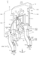
- FIG. 1 is a schematic perspective view showing the semiconductor device of the first embodiment.
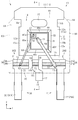
- FIG. 2 is a schematic plan view of the semiconductor device of the first embodiment.
- FIG. 3 is a schematic back view of the semiconductor device of the first embodiment.
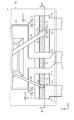
- FIG. 4 is a cross-sectional view taken along the line 4-4 of FIG.
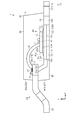
- FIG. 5 is a schematic side view of the semiconductor device of the first embodiment.
- FIG. 6 is a partially enlarged plan view showing the semiconductor device of the first embodiment.
- FIG. 7 is a partially enlarged plan view showing the semiconductor device of the modified example of the first embodiment.
- FIG. 8 is a partially enlarged plan view showing the semiconductor device of the modified example of the first embodiment.
- FIG. 9 is a schematic perspective view showing the semiconductor device of the second embodiment.
- FIG. 10 is a schematic plan view of the semiconductor device of the second embodiment.
- FIG. 11 is a schematic back view of the semiconductor device of the second embodiment.
- FIG. 12 is a cross-sectional view taken along the line 12-12 of FIG.
- FIG. 13 is a schematic side view of the semiconductor device of the second embodiment.
- FIG. 14 is a schematic side view of the semiconductor device of the second embodiment.
- FIG. 15 is a cross-sectional photograph showing the drive pad and the sealing resin.
- the semiconductor device 1 includes a substrate 10, a drive lead 20, a control lead 30, a semiconductor element 40, a drive wire 50, a control wire 60, and a sealing resin 80.
- the sealing resin 80 seals the semiconductor element 40, the control wire 60, and the drive wire 50.
- the sealing resin 80 is formed so as to expose a part of the substrate 10, the drive lead 20, and the control lead 30.
- the drive lead 20 has an outer lead 20A protruding from the sealing resin 80 and an inner lead 20B provided in the sealing resin 80 and electrically connected to the outer lead 20A.
- the outer lead 20A and the inner lead 20B are an integrated single component.
- the control lead 30 has an outer lead 30A protruding from the sealing resin 80 and an inner lead 30B provided in the sealing resin 80 and electrically connected to the outer lead 30A.
- the outer lead 30A and the inner lead 30B are an integrated single component.
- the semiconductor device 1 of this embodiment is a TO (Transistor Outline) -252 package defined in the package outline standard (JEITA standard). Further, the semiconductor device 1 is a so-called SIP (Single Inline Package) type in which the outer lead 20A of the drive lead 20 and the outer lead 30A of the control lead 30 extend from one surface of the sealing resin 80, respectively.
- the shape of the sealing resin 80 is a rectangular parallelepiped.
- the sealing resin 80 is shown by a chain double-dashed line, and the parts inside the sealing resin 80 are shown by a solid line.
- the sealing resin 80 is a synthetic resin having electrical insulation.
- the sealing resin 80 is an epoxy resin.
- the sealing resin 80 includes a first sealing resin side surface 81, a second sealing resin side surface 82, a third sealing resin side surface 83, a fourth sealing resin side surface 84, a sealing resin back surface 85, and a sealing resin top surface. It has 6 faces of 86.
- the first sealing resin side surface 81 and the second sealing resin side surface 82 face each other at intervals.
- the third sealing resin side surface 83 and the fourth sealing resin side surface 84 face each other at intervals.
- the sealing resin back surface 85 and the sealing resin top surface 86 face each other at intervals.
- the direction in which the sealing resin back surface 85 and the sealing resin top surface 86 are arranged is the thickness direction Z, and the first sealing resin side surface 81 and the second sealing resin side surface 82 are arranged.
- the direction is the vertical direction X
- the direction in which the third sealing resin side surface 83 and the fourth sealing resin side surface 84 are arranged is the horizontal direction Y.
- the vertical direction X and the horizontal direction Y are directions orthogonal to the thickness direction Z.
- the vertical direction X is a direction orthogonal to the horizontal direction Y.
- the thickness direction Z corresponds to the first direction
- the vertical direction X corresponds to the second direction
- the horizontal direction Y corresponds to the third direction.
- the shape of the sealing resin 80 is a rectangular parallelepiped.
- the sealing resin 80 is a synthetic resin having electrical insulation.
- the sealing resin 80 is an epoxy resin.
- the sealing resin 80 includes a first sealing resin side surface 81, a second sealing resin side surface 82, a third sealing resin side surface 83, a fourth sealing resin side surface 84, a sealing resin back surface 85, and a sealing resin top surface. It has 6 faces of 86.
- the first sealing resin side surface 81 and the second sealing resin side surface 82 face each other at intervals.
- the third sealing resin side surface 83 and the fourth sealing resin side surface 84 face each other at intervals.
- the sealing resin back surface 85 and the sealing resin top surface 86 face each other at intervals.
- the direction in which the sealing resin back surface 85 and the sealing resin top surface 86 are arranged is the thickness direction Z, and the first sealing resin side surface 81 and the second sealing resin side surface 82 are arranged.
- the direction is the vertical direction X
- the direction in which the third sealing resin side surface 83 and the fourth sealing resin side surface 84 are arranged is the horizontal direction Y.
- the vertical direction X and the horizontal direction Y are directions orthogonal to the thickness direction Z.
- the vertical direction X is a direction orthogonal to the horizontal direction Y.
- the vertical direction X corresponds to the first direction
- the horizontal direction Y corresponds to the second direction.
- FIG. 2 is a view of the semiconductor device 1 as viewed from the top surface 86 of the sealing resin in the thickness direction Z.
- the shape of the sealing resin 80 is such that the vertical direction X is the long side direction and the horizontal direction Y is the short side direction. It has a substantially rectangular shape. Viewing from the thickness direction Z is hereinafter referred to as plan view.
- the first sealing resin side surface 81 and the second sealing resin side surface 82 are side surfaces along the horizontal direction Y
- the third sealing resin side surface 83 and the fourth sealing resin side surface 84 are along the vertical direction X. The side.
- the substrate 10 has a main surface 10a and a back surface 10b (see FIG. 3) facing opposite sides in the thickness direction Z.
- the main surface 10a faces the same direction as the sealing resin top surface 86
- the back surface 10b faces the same direction as the sealing resin back surface 85.
- the substrate 10 is made of, for example, Cu (copper).
- the term "composed of Cu” means that it is made of Cu or an alloy containing Cu.
- the substrate 10 has a flat plate-shaped substrate main body portion 11 and a lead portion 16. In the present embodiment, the substrate main body portion 11 and the lead portion 16 are integrated into a single component.
- the substrate main body 11 can be divided into an inner main body 12 covered with the sealing resin 80 and a protruding portion 13 protruding from the sealing resin 80.
- the inner main body portion 12 and the protruding portion 13 are adjacent to each other in the vertical direction X.
- the protruding portion 13 projects from the side surface 81 of the first sealing resin in the vertical direction X.
- the size of the protruding portion 13 in the lateral direction Y is smaller than the size of the inner main body portion 12 in the lateral direction Y.
- the size of the protruding portion 13 in the lateral direction Y can be arbitrarily changed. In one example, the size of the protruding portion 13 in the lateral direction Y may be equal to the size of the inner main body portion 12 in the lateral direction Y.
- the inner main body portion 12 is arranged so that the center of the inner main body portion 12 is closer to the side surface 81 of the first sealing resin than the center of the sealing resin 80 in the vertical direction X.
- the inner main body portion 12 has a main surface 12a, a back surface 12b (see FIG. 3), a first side surface 12c, a second side surface 12d, and a third side surface 12e.
- the main surface 12a and the back surface 12b face each other in the thickness direction Z.
- the main surface 12a constitutes a part of the main surface 10a of the substrate 10
- the back surface 12b constitutes the back surface 10b of the substrate 10.
- the main surface 12a faces the sealing resin top surface 86 side
- the back surface 12b faces the sealing resin back surface 85 side.
- the first side surface 12c faces the second sealing resin side surface 82
- the second side surface 12d faces the third sealing resin side surface 83
- the third side surface 12e faces the fourth sealing resin side surface 84.
- the first side surface 12c extends along the lateral direction Y.
- the second side surface 12d and the third side surface 12e face each other with a gap in the lateral direction Y.
- the second side surface 12d and the third side surface 12e extend along the vertical direction X.
- a narrow portion 14 is formed at the end of the inner main body portion 12 on the protruding portion 13 side.
- the narrow portion 14 has a recess 14a recessed from the second side surface 12d toward the fourth sealing resin side surface 84 side in the lateral direction Y, and the narrow portion 14 toward the third sealing resin side surface 83 side in the lateral direction Y from the third side surface 12e. It is formed by a recess 14b that is recessed.
- the size of the narrow portion 14 in the lateral direction Y is smaller than the size of the portion of the inner main body portion 12 other than the narrow portion 14 in the lateral direction. Further, the size of the narrow portion 14 in the lateral direction Y is smaller than the size of the protruding portion 13 in the lateral direction Y.
- the narrow portion 14 is provided so as to be adjacent to the first sealing resin side surface 81 of the sealing resin 80 in the vertical direction X.
- the narrow portion 14 is provided with a through hole 15 penetrating the narrow portion 14 in the thickness direction Z.
- the shape of the through hole 15 in a plan view is an ellipse in which the lateral direction Y is the longitudinal direction.
- the inner main body portion 12 has flange portions 19a and 19b protruding from the main body side surface of the inner main body portion 12.
- the flange portion 19a projects from the second side surface 12d of the inner main body portion 12 toward the third sealing resin side surface 83.
- the flange portion 19b projects from the third side surface 12e of the inner main body portion 12 toward the fourth sealing resin side surface 84.
- the flange portions 19a and 19b are provided so as to be flush with the main surface 12a of the inner main body portion 12, respectively. Therefore, the main surface 10a of the substrate 10 is composed of the main surface 12a of the inner main body portion 12 and the flange portions 19a and 19b. Further, the flange portions 19a and 19b are provided so as to be on the main surface 12a side of the back surface 12b of the inner main body portion 12, respectively. Therefore, the back surface 10b of the substrate 10 is composed of the back surface 12b of the inner main body 12.
- the flange portions 19a and 19b suppress the separation of the substrate 10 and the sealing resin 80.
- the back surface 10b of the substrate 10 (the back surface 12b of the inner main body 12) is exposed from the back surface 85 of the sealing resin.
- the sealing resin 80 has entered the recesses 14a and 14b and the through holes 15 of the narrow portion 14 of the inner main body portion 12. As a result, the separation between the substrate 10 and the sealing resin 80 can be further suppressed.
- the lead portion 16 extends from the end portion of the inner main body portion 12 on the first side surface 12c side toward the second sealing resin side surface 82 and the second sealing resin side surface 82. Protruding from.
- the lead portion 16 can be divided into a terminal portion 17 protruding from the side surface 82 of the second sealing resin and a connecting portion 18 connecting the terminal portion 17 and the inner main body portion 12.
- the connecting portion 18 is located on the second side surface 12d side of the central portion of the inner main body portion 12 in the lateral direction Y.
- the connecting portion 18 is continuous from the flange portion 19a. That is, the thickness of the portion of the connecting portion 18 connected to the inner main body portion 12 is thicker than the thickness of the flange portions 19a and 19b and thinner than the thickness of the inner main body portion 12.
- the connecting portion 18 has an inclined portion 18a.
- the inclined portion 18a is inclined toward the sealing resin top surface 86 from the first side surface 12c of the inner main body portion 12 toward the second sealing resin side surface 82.
- the intermediate portion 18b between the inclined portion 18a and the terminal portion 17 of the connecting portion 18 is located on the sealing resin top surface 86 side of the main surface 12a of the inner main body portion 12.
- the intermediate portion 18b has a bent portion 18c that bends toward the side surface 84 of the fourth sealing resin.
- the portion of the intermediate portion 18b that comes into contact with the second sealing resin side surface 82 is located at the central portion of the second sealing resin side surface 82 in the lateral direction Y.
- the terminal portion 17 protrudes from the central portion of the second sealing resin side surface 82 in the lateral direction Y. In the thickness direction Z, the position of the terminal portion 17 is the same as the position of the intermediate portion 18b. That is, the terminal portion 17 is located on the sealing resin top surface 86 side of the main surface 12a of the inner main body portion 12.
- the drive lead 20 and the control lead 30 are separated from the substrate 10 in the vertical direction X on the second sealing resin side surface 82 side of the sealing resin 80. It is arranged in the state.
- the drive lead 20 and the control lead 30 are arranged so as to be separated from each other in the lateral direction Y.
- a lead portion 16 is arranged between the drive lead 20 and the control lead 30 in the lateral direction Y.
- the drive lead 20 has a drive pad 21, a drive terminal 22, and a connecting portion 23 that connects the drive pad 21 and the drive terminal 22.
- the drive pad 21 and the connecting portion 23 form an inner lead 20B, and the drive terminal 22 constitutes an outer lead 20A.
- the drive pad 21 and the connecting portion 23 are arranged between the substrate 10 and the second sealing resin side surface 82 in the vertical direction X.
- the drive pad 21 and the connecting portion 23 are arranged on the side surface 84 side of the fourth sealing resin in the lateral direction Y with respect to the central portion of the sealing resin 80 in the lateral direction Y.
- the drive lead 20 is made of Cu in this embodiment. That is, the drive lead 20 is made of the same material as the substrate 10.
- the shape of the drive pad 21 in a plan view is a rectangular shape in which the horizontal direction Y is the long side direction and the vertical direction X is the short side direction.
- the drive pad 21 has a first end portion 21a and a second end portion 21b which are both end portions in the lateral direction Y.
- the drive pad 21 is located on the sealing resin top surface 86 side of the main surface 12a of the inner main body portion 12 in the thickness direction Z. Further, the drive pad 21 is located on the sealing resin top surface 86 side of the main surface 40a of the semiconductor element 40 in the thickness direction Z.
- the drive pad 21 is at the same position as the intermediate portion 18b of the lead portion 16 in the thickness direction Z.
- the connecting portion 23 is continuous from the end portion of the drive pad 21 on the side surface 82 side of the second sealing resin.
- the connecting portion 23 is located on the side surface 84 side of the fourth sealing resin with respect to the central portion of the drive pad 21 in the lateral direction Y.
- the drive terminal 22 constitutes a source terminal. As shown in FIG. 5, the drive terminal 22 projects from the first inclined surface 82a of the second sealing resin side surface 82.
- the control lead 30 has a control pad 31, a control terminal 32, and a connecting portion 33 that connects the control pad 31 and the control terminal 32.
- the control pad 31 and the connecting portion 33 form an inner lead 30B, and the control terminal 32 constitutes an outer lead 30A.
- the control pad 31 and the connecting portion 33 are arranged between the substrate 10 and the second sealing resin side surface 82 in the vertical direction X.
- the control pad 31 and the connecting portion 33 are arranged on the side surface 83 side of the third sealing resin 80 with respect to the central portion of the sealing resin 80 in the lateral direction Y.
- the control lead 30 is made of Cu in this embodiment. That is, the control lead 30 is made of the same material as the substrate 10 and the drive lead 20.
- the shape of the control pad 31 in a plan view is a substantially rectangular shape in which the horizontal direction Y is the long side direction and the vertical direction X is the short side direction.
- the control pad 31 has a first end portion 31a and a second end portion 31b which are both end portions in the lateral direction Y.
- the size of the control pad 31 in the lateral direction Y is smaller than the size of the drive pad 21 in the lateral direction Y.
- the control pad 31 is located on the sealing resin top surface 86 side of the main surface 12a of the inner main body portion 12 in the thickness direction Z. Further, the control pad 31 is located on the sealing resin top surface 86 side of the main surface 40a of the semiconductor element 40 in the thickness direction Z. In the present embodiment, the control pad 31 is at the same position as the intermediate portion 18b of the lead portion 16 in the thickness direction Z.
- the connecting portion 33 is continuous from the end portion of the control pad 31 on the side surface 82 side of the second sealing resin.
- the connecting portion 33 is located closer to the third sealing resin side surface 83 of the control pad 31 in the lateral direction Y.
- the control terminal 32 constitutes a gate terminal.
- the control terminal 32 projects from the first inclined surface 82a of the second sealing resin side surface 82.
- the drive pad 21 has a connecting surface 24 facing the same direction as the main surface 10a of the substrate 10.
- a plating layer 71 is formed on the connection surface 24 to cover a part of the connection surface 24.
- the plating layer 71 is made of, for example, Ni (nickel). By being composed of Ni, it is intended that it is formed of Ni or an alloy containing Ni.
- the plating layer 71 is formed in the center of the drive pad 21 in the short side direction and the vertical direction X of the drive pad 21. Further, the plating layer 71 extends from the first end portion 21a to the second end portion 21b of the drive pad 21 along the long side direction of the drive pad 21, that is, the lateral direction Y. Therefore, the connection surface 24 of the drive pad 21 has a portion 24a covered with the plating layer 71 and a portion 24b exposed from the plating layer 71.
- the control pad 31 has a connecting surface 34 facing the same direction as the main surface 10a of the substrate 10.
- a plating layer 72 that covers a part of the connection surface 34 is formed on the connection surface 34.
- the plating layer 72 is made of, for example, Ni. By being composed of Ni, it is intended that it is formed of Ni or an alloy containing Ni.
- the plating layer 72 is formed in the center of the control pad 31 in the short side direction and the vertical direction X of the control pad 31. Further, the plating layer 72 extends from the first end portion 31a to the second end portion 31b of the control pad 31 along the long side direction of the control pad 31, that is, the lateral direction Y. Therefore, the connection surface 34 of the control pad 31 has a portion 34a covered with the plating layer 72 and a portion 34b exposed from the plating layer 72.
- the plating layer 71 formed on the drive pad 21 and the plating layer 72 formed on the control pad 31 are at the same position in the vertical direction X. Further, in the vertical direction X, the width W71 of the plating layer 71 formed on the drive pad 21 is equal to the width W72 of the plating layer 72 formed on the control pad 31. Therefore, the plating layer 71 formed on the drive pad 21 and the plating layer 72 formed on the control pad 31 overlap each other when viewed from the lateral direction Y.
- the end portion on the inclined portion 18a side is located at the same height as the drive pad 21 and the control pad 31.
- the plating layers 71 and 72 are formed, for example, on the upper surface of the intermediate portion 18b, a plating layer 73 that overlaps with the plating layers 71 and 72 when viewed from the lateral direction Y.
- the semiconductor element 40 is mounted on the main surface 12a of the inner main body portion 12 by solder SD. As shown in FIG. 2, in the present embodiment, the semiconductor element 40 is arranged in the central portion of the inner main body portion 12. Further, the semiconductor element 40 and the drive pad 21 are displaced in the vertical direction X. Further, the semiconductor element 40 and the control pad 31 are displaced in the vertical direction X.
- the semiconductor element 40 is a silicon carbide (SiC) chip.
- SiC MOSFET metal-oxide-semiconductor field-effect transistor
- the semiconductor element 40 SiCMOSFT is an element capable of high-speed switching.
- the switching frequency is, for example, 1 kHz or more and several hundred kHz or less.
- the semiconductor element 40 is formed in a flat plate shape. Specifically, in a plan view, the shape of the semiconductor element 40 is, for example, a square shape. As shown in FIGS. 2 and 4, the semiconductor element 40 has a main surface 40a, a back surface 40b, and a plurality of side surfaces 40c to 40f. The main surface 40a and the back surface 40b face each other in the thickness direction Z.
- the main surface 40a faces the sealing resin top surface 86. That is, the main surface 40a faces the same direction as the main surface 10a of the substrate 10.
- the back surface 40b faces the back surface 85 of the sealing resin.
- the back surface 40b faces the main surface 12a of the inner main body 12.
- the side surface 40c faces the first sealing resin side surface 81
- the side surface 40d faces the second sealing resin side surface 82
- the side surface 40e faces the third sealing resin side surface 83
- the side surface 40f faces the fourth sealing resin side surface. It faces the side surface 84.
- a main surface side drive electrode 41 and a control electrode 43 are formed on the main surface 40a.
- the main surface side drive electrode 41 and the control electrode 43 form a main surface electrode formed on the main surface 40a of the semiconductor element 40.
- a back surface side drive electrode 42 (see FIG. 4) is formed on the back surface 40b.
- the main surface side drive electrode 41 constitutes the source electrode
- the back surface side drive electrode 42 constitutes the drain electrode.
- the control electrode 43 constitutes a gate electrode.
- the back surface side drive electrode 42 is electrically connected to the inner main body portion 12 by a solder SD.
- the solder SD is, for example, lead solder.
- the semiconductor element 40 has a passivation film formed on the main surface 40a.
- the passivation film is formed with an opening that exposes the electrodes on the main surface 40a side of the semiconductor element 40 as the main surface side drive electrodes 41 and the control electrodes 43.
- the semiconductor device 1 includes one drive wire 50 and one control wire 60.
- the drive wire 50 and the control wire 60 are made of the same metal.
- the drive wire 50 and the control wire 60 are made of Al (aluminum). By being composed of Al, it is intended that it is formed of Al or an alloy containing Al.
- the drive wire 50 has a circular cross-sectional shape perpendicular to the major axis direction near the center.
- the control wire 60 has a circular cross-sectional shape perpendicular to the major axis direction near the center.
- the wire diameter of the drive wire 50 is larger than the wire diameter of the control wire 60. That is, the drive wire 50 is a large-diameter aluminum wire.
- the wire diameter of the drive wire 50 is, for example, 200 ⁇ m or more and 600 ⁇ m or less.
- the wire diameter of the control wire 60 is, for example, 40 ⁇ m or more and 100 ⁇ m or less.
- the first end 51 of the drive wire 50 is joined to the main surface side drive electrode 41 of the semiconductor element 40, and the second end 52 of the drive wire 50 is formed on a plating layer 71 that covers a part of the connection surface 24 of the drive pad 21. It is joined.
- the drive wire 50 is bonded to the main surface side drive electrode 41 and the drive pad 21 by, for example, ultrasonic bonding.
- the joint portion 53 of the second end 52 of the drive wire 50 is a portion 53a joined to the upper surface of the plating layer 71 and a portion 24b exposed from the plating layer 71 of the connection surface 24 of the drive pad 21. It has a portion 53b joined to. As shown in FIG.
- the area of the portion 53a of the upper surface of the plating layer 71 where the second end 52 of the drive wire 50 and the plating layer 71 are joined is a cross section perpendicular to the long axis direction of the drive wire 50. It is more than the area. That is, the width W71 in the vertical direction X of the plating layer 71 is set so that the bonding area between the plating layer 71 and the drive wire 50 bonded to the plating layer 71 is equal to or larger than the cross-sectional area of the drive wire 50.
- the joining portion 53 shows an example having the portion 53a and the portion 53b, but the width W71 of the plating layer 71 is set so that all the joining portions 53 are joined to the plating layer 71. You may.
- the first end 61 of the control wire 60 is joined to the control electrode 43 of the semiconductor element 40, and the second end 62 of the control wire 60 is one of the connection surfaces 34 of the control pad 31. It is joined to the plating layer 72 that covers the portion.
- the control wire 60 is bonded to the control electrode 43 and the control pad 31 by, for example, ultrasonic bonding.
- the joint portion 63 of the second end 62 of the control wire 60 is joined only to the upper surface of the plating layer 72. That is, the plating layer 72 is set to have a width W72 in the vertical direction X so that the joint portion 63 of the second end 62 of the control wire 60 to be joined does not protrude.
- the semiconductor element 40 is mounted on the main surface 10a of the substrate 10, and the connection surfaces 24 and 34 of the drive pad 21 and the control pad 31 made of Cu are made of Ni and are made of Ni.
- Plating layers 71 and 72 that cover a part of 34 are formed.
- the first end 51 of the drive wire 50 made of Al is joined to the main surface side drive electrode 41 of the semiconductor element 40, and the second end 52 of the drive wire 50 is the plating layer 71 on the connection surface 24 of the drive pad 21. It is joined to.
- the first end 61 of the control wire 60 made of Al is bonded to the control electrode 43 of the semiconductor element 40, and the second end 62 of the control wire 60 is bonded to the plating layer 72 on the connection surface 34 of the control pad 31. ing.
- the semiconductor element 40, the drive pad 21, the control pad 31, the plating layers 71 and 72, the drive wire 50, and the control wire 60 are sealed with the sealing resin 80.
- the connection surface 24 of the drive pad 21 has a portion 24a covered with the plating layer 71 and a portion 24b exposed from the plating layer 71.
- the plating layer 71 made of Ni prevents the drive wire 50 from separating from the drive pad 21.
- the drive wire 50 made of Al is directly bonded to the drive pad 21 made of Cu, the intermetallic compound held between the drive wire 50 and the drive pad 21 grows due to heat, and the drive wire 50 is driven.
- the pad 21 may be separated from the pad 21. Therefore, the plating layer 71 made of Ni prevents the formation of intermetallic compounds and prevents the drive wire 50 from separating from the drive pad 21.
- the portion 24b exposed from the plating layer 71 on the connection surface 24 of the drive pad 21 is the surface of the drive pad 21 made of Cu, and has good adhesion to the sealing resin 80. Therefore, this portion 24b suppresses the peeling of the sealing resin 80 from the drive pad 21.
- the sealing resin 80 is peeled from the drive pad 21, the drive wire 50 joined to the drive pad 21 may be broken due to the peeling. Therefore, the portion 24b exposed from the plating layer 71 suppresses the peeling of the sealing resin 80 from the drive pad 21, and suppresses the disconnection of the drive wire 50.
- the connection surface 34 of the control pad 31 has a portion 34a covered with the plating layer 72 and a portion 34b exposed from the plating layer 72.
- the plating layer 72 made of Ni prevents the control wire 60 from being separated from the control pad 31.
- the control wire 60 made of Al is directly bonded to the control pad 31 made of Cu, the intermetallic compound held between the control wire 60 and the control pad 31 grows due to heat, and the control wire 60 controls the control wire 60.
- the pad 31 may be separated from the pad 31. Therefore, the plating layer 72 made of Ni prevents the formation of intermetallic compounds and prevents the control wire 60 from separating from the control pad 31.
- the portion 34b exposed from the plating layer 72 on the connection surface 34 of the control pad 31 is the surface of the control pad 31 made of Cu, and has good adhesion to the sealing resin 80. Therefore, this portion 34b suppresses the peeling of the sealing resin 80 from the control pad 31.
- the portion 34b exposed from the plating layer 72 suppresses the peeling of the sealing resin 80 from the control pad 31, and suppresses the disconnection of the control wire 60.
- a large-diameter drive wire 50 made of Al is used between the main surface side drive electrode 41 of the semiconductor element 40 and the drive pad 21. ing.
- a wire such as Au (gold) or Cu
- a plurality of wires must be connected according to the current, which leads to an increase in man-hours for connection and an increase in pad area, that is, an increase in the size of the semiconductor device.
- a required current can be passed by one drive wire 50, and an increase in man-hours and an increase in size can be suppressed.
- the semiconductor element 40 is mounted on the main surface 10a of the substrate 10, and the connection surfaces 24 and 34 of the drive pad 21 made of Cu and the control pad 31 are made of Ni and cover a part of the connection surfaces 24 and 34.
- Plating layers 71 and 72 are formed.
- the first end 51 of the drive wire 50 made of Al is joined to the main surface side drive electrode 41 of the semiconductor element 40, and the second end 52 of the drive wire 50 is the plating layer 71 on the connection surface 24 of the drive pad 21. It is joined to.
- the first end 61 of the control wire 60 made of Al is bonded to the control electrode 43 of the semiconductor element 40, and the second end 62 of the control wire 60 is bonded to the plating layer 72 on the connection surface 34 of the control pad 31. ing.
- the semiconductor element 40, the drive pad 21, the control pad 31, the plating layers 71 and 72, the drive wire 50, and the control wire 60 are sealed with the sealing resin 80.
- the plating layer 72 made of Ni can prevent the control wire 60 from being separated from the control pad 31.
- the portion 24b exposed from the plating layer 71 on the connection surface 24 of the drive pad 21 has good adhesion to the sealing resin 80, suppresses peeling of the sealing resin 80 from the drive pad 21, and suppresses disconnection of the drive wire 50. can.
- the plating layer 71 made of Ni can prevent the drive wire 50 from being separated from the drive pad 21.
- the portion 24b exposed from the plating layer 71 on the connection surface 34 of the drive pad 21 has good adhesion to the sealing resin 80, suppresses peeling of the sealing resin 80 from the drive pad 21, and suppresses disconnection of the drive wire 50. can.
- the semiconductor device 101 includes a substrate 110, a drive lead 120, a control lead 130, a semiconductor element 140, a drive wire 150, a control wire 160, and a sealing resin 180.
- the sealing resin 180 seals the semiconductor element 140, the control wire 160, and the drive wire 150.
- the sealing resin 180 is formed so as to expose a part of the substrate 110, the drive lead 120, and the control lead 130.
- the drive lead 120 has an outer lead 120A protruding from the sealing resin 180 and an inner lead 120B provided in the sealing resin 180 and electrically connected to the outer lead 120A.
- the outer lead 120A and the inner lead 120B are an integrated single component.
- the control lead 130 has an outer lead 130A protruding from the sealing resin 180, and an inner lead 130B provided in the sealing resin 180 and electrically connected to the outer lead 130A.
- the outer lead 130A and the inner lead 130B are an integrated single component.
- the semiconductor device 101 of this embodiment is a TO (Transistor Outline) -252 package defined in the package outline standard (JEITA standard). Further, the semiconductor device 101 is a so-called SIP (Single Inline Package) type in which the outer lead 120A of the drive lead 120 and the outer lead 130A of the control lead 130 extend from one surface of the sealing resin 180, respectively.
- the shape of the sealing resin 180 is a rectangular parallelepiped.
- the sealing resin 180 is indicated by a chain double-dashed line, and the parts inside the sealing resin 180 are indicated by a solid line.
- the sealing resin 180 is a synthetic resin having electrical insulation.
- the sealing resin 180 is an epoxy resin.
- the sealing resin 180 includes a first sealing resin side surface 181, a second sealing resin side surface 182, a third sealing resin side surface 83, a fourth sealing resin side surface 184, a sealing resin back surface 185, and a sealing resin top surface. It has 6 faces of 186.
- the first sealing resin side surface 181 and the second sealing resin side surface 182 face each other at intervals.
- the third sealing resin side surface 83 and the fourth sealing resin side surface 184 face each other at intervals.
- the sealing resin back surface 185 and the sealing resin top surface 186 face each other at intervals.
- the direction in which the sealing resin back surface 185 and the sealing resin top surface 186 are arranged is defined as the thickness direction Z, and the first sealing resin side surface 181 and the second sealing resin side surface 182 are arranged.
- the direction is the vertical direction X
- the direction in which the third sealing resin side surface 83 and the fourth sealing resin side surface 184 are arranged is the horizontal direction Y.
- the vertical direction X and the horizontal direction Y are directions orthogonal to the thickness direction Z.
- the vertical direction X is a direction orthogonal to the horizontal direction Y.
- the thickness direction Z corresponds to the first direction
- the vertical direction X corresponds to the second direction
- the horizontal direction Y corresponds to the third direction.
- the shape of the sealing resin 180 is a rectangular parallelepiped.
- the sealing resin 180 is a synthetic resin having electrical insulation.
- the sealing resin 180 is an epoxy resin.
- the sealing resin 180 includes a first sealing resin side surface 181, a second sealing resin side surface 182, a third sealing resin side surface 83, a fourth sealing resin side surface 184, a sealing resin back surface 185, and a sealing resin top surface. It has 6 faces of 186.
- the first sealing resin side surface 181 and the second sealing resin side surface 182 face each other at intervals.
- the third sealing resin side surface 83 and the fourth sealing resin side surface 184 face each other at intervals.
- the sealing resin back surface 185 and the sealing resin top surface 186 face each other at intervals.
- the direction in which the sealing resin back surface 185 and the sealing resin top surface 186 are arranged is defined as the thickness direction Z, and the first sealing resin side surface 181 and the second sealing resin side surface 182 are arranged.
- the direction is the vertical direction X
- the direction in which the third sealing resin side surface 83 and the fourth sealing resin side surface 184 are arranged is the horizontal direction Y.
- the vertical direction X and the horizontal direction Y are directions orthogonal to the thickness direction Z.
- the vertical direction X is a direction orthogonal to the horizontal direction Y.
- the vertical direction X corresponds to the first direction
- the horizontal direction Y corresponds to the second direction.
- FIG. 10 is a view of the semiconductor device 101 as viewed from the top surface 186 of the sealing resin in the thickness direction Z.
- the shape of the sealing resin 180 is such that the vertical direction X is the long side direction and the horizontal direction Y is the short side direction. It has a substantially rectangular shape. Viewing from the thickness direction Z is hereinafter referred to as plan view.
- the first sealing resin side surface 181 and the second sealing resin side surface 182 are side surfaces along the horizontal direction Y
- the third sealing resin side surface 83 and the fourth sealing resin side surface 184 are along the vertical direction X. The side.
- the substrate 110 has a main surface 110a and a back surface 110b (see FIG. 11) facing opposite sides in the thickness direction Z.
- the main surface 110a faces the same direction as the sealing resin top surface 186
- the back surface 110b faces the same direction as the sealing resin back surface 185.
- the substrate 110 has a flat plate-shaped substrate main body 111 and a lead 116. In the present embodiment, the substrate main body 111 and the lead 116 are integrated as a single component.
- the substrate main body 111 is a die bonding pad on which the semiconductor element 140 is mounted.
- the substrate main body 111 can be divided into an inner main body 112 covered with the sealing resin 180 and a protruding portion 113 protruding from the sealing resin 180.
- the inner main body portion 112 and the protruding portion 113 are adjacent to each other in the vertical direction X.
- the protruding portion 113 protrudes from the side surface 181 of the first sealing resin in the vertical direction X.
- the size of the protruding portion 113 in the lateral direction Y is smaller than the size of the inner main body portion 112 in the lateral direction Y.
- the size of the protruding portion 113 in the lateral direction Y can be arbitrarily changed. In one example, the size of the protruding portion 113 in the lateral direction Y may be equal to the size of the inner main body portion 112 in the lateral direction Y.
- the inner main body portion 112 is arranged so that the center of the inner main body portion 112 is closer to the side surface 181 of the first sealing resin than the center of the sealing resin 180 in the vertical direction X.
- the inner main body portion 112 has a main surface 112a, a back surface 112b (see FIG. 11), a first side surface 112c, a second side surface 112d, and a third side surface 112e.
- the main surface 112a and the back surface 112b face each other in the thickness direction Z.
- the main surface 112a constitutes a part of the main surface 110a of the substrate 110
- the back surface 112b constitutes the back surface 110b of the substrate 110.
- the main surface 112a faces the sealing resin top surface 186 side
- the back surface 112b faces the sealing resin back surface 185 side
- the first side surface 112c faces the second sealing resin side surface 182
- the second side surface 112d faces the third sealing resin side surface 83
- the third side surface 112e faces the fourth sealing resin side surface 184.
- the first side surface 112c extends along the lateral direction Y.
- the second side surface 112d and the third side surface 112e face each other with a gap in the lateral direction Y.
- the second side surface 112d and the third side surface 112e extend along the vertical direction X.
- a narrow portion 114 is formed at the end of the inner main body portion 112 on the protruding portion 113 side.
- the narrow portion 114 has a recess 114a recessed from the second side surface 112d toward the fourth sealing resin side surface 184 side in the lateral direction Y, and the narrow portion 114 toward the third sealing resin side surface 83 side in the lateral direction Y from the third side surface 112e. It is formed by a recess 114b that is recessed.
- the size of the narrow portion 114 in the lateral direction Y is smaller than the size of the portion of the inner main body portion 112 other than the narrow portion 114 in the lateral direction.
- the size of the narrow portion 114 in the lateral direction Y is smaller than the size of the protruding portion 113 in the lateral direction Y.
- the narrow portion 114 is provided so as to be adjacent to the first sealing resin side surface 181 of the sealing resin 180 in the vertical direction X.
- the narrow portion 114 is provided with a through hole 115 penetrating the narrow portion 114 in the thickness direction Z.
- the shape of the through hole 115 in a plan view is an ellipse in which the lateral direction Y is the longitudinal direction.
- the inner main body 112 has flanges 119a and 119b protruding from the side surface of the inner main body 112.
- the flange portion 119a projects from the second side surface 112d of the inner main body portion 112 toward the third sealing resin side surface 83.
- the flange portion 119b projects from the third side surface 112e of the inner main body portion 112 toward the fourth sealing resin side surface 184.
- the flange portions 119a and 119b are provided so as to be flush with the main surface 112a of the inner main body portion 112, respectively. Therefore, the main surface 110a of the substrate 110 is composed of the main surface 112a of the inner main body portion 112 and the flange portions 119a and 119b. Further, the flange portions 119a and 119b are provided so as to be closer to the main surface 112a than the back surface 112b of the inner main body portion 112, respectively. Therefore, the back surface 110b of the substrate 110 is composed of the back surface 112b of the inner main body 112.
- the flange portions 119a and 119b suppress the separation of the substrate 110 and the sealing resin 180.
- the back surface 110b of the substrate 110 (the back surface 112b of the inner main body 112) is exposed from the back surface 185 of the sealing resin.
- the sealing resin 180 has entered the recesses 114a and 114b and the through holes 115 of the narrow portion 114 of the inner main body 112, respectively. As a result, the separation between the substrate 110 and the sealing resin 180 can be further suppressed.
- the lead portion 116 extends from the end of the inner main body portion 112 on the first side surface 112c side toward the second sealing resin side surface 182 and the second sealing resin side surface 182. Protruding from.
- the lead portion 116 can be divided into a terminal portion 117 protruding from the side surface 182 of the second sealing resin and a connecting portion 118 connecting the terminal portion 117 and the inner main body portion 112.
- the connecting portion 118 is located on the second side surface 112d side of the central portion of the inner main body portion 112 in the lateral direction Y.
- the connecting portion 118 is continuous from the flange portion 119a. That is, the thickness of the portion of the connecting portion 118 connected to the inner main body portion 112 is thicker than the thickness of the flange portions 119a and 119b and thinner than the thickness of the inner main body portion 112.
- the connecting portion 118 has an inclined portion 118a.
- the inclined portion 118a is inclined toward the sealing resin top surface 186 from the first side surface 112c of the inner main body portion 112 toward the second sealing resin side surface 182.
- the intermediate portion 118b between the inclined portion 118a and the terminal portion 117 of the connecting portion 118 is located on the sealing resin top surface 186 side of the main surface 112a of the inner main body portion 112.
- the intermediate portion 118b has a bent portion 118c that bends toward the side surface 184 of the fourth sealing resin.
- the portion of the intermediate portion 118b that comes into contact with the second sealing resin side surface 182 is located at the central portion of the second sealing resin side surface 182 in the lateral direction Y.
- the terminal portion 117 protrudes from the central portion of the second sealing resin side surface 182 in the lateral direction Y. In the thickness direction Z, the position of the terminal portion 117 is the same as the position of the intermediate portion 118b. That is, the terminal portion 117 is located on the sealing resin top surface 186 side of the main surface 112a of the inner main body portion 112.
- the drive lead 120 and the control lead 130 are separated from the substrate 110 in the vertical direction X on the second sealing resin side surface 182 side of the sealing resin 180. It is arranged in the state.
- the drive lead 120 and the control lead 130 are arranged so as to be separated from each other in the lateral direction Y.
- a lead portion 116 is arranged between the drive lead 120 and the control lead 130 in the lateral direction Y.
- the drive lead 120 has a drive pad 121, a drive terminal 122, and a connecting portion 1123 that connects the drive pad 121 and the drive terminal 122.
- the drive pad 121 and the connecting portion 1123 form an inner lead 120B, and the drive terminal 122 constitutes an outer lead 120A.
- the drive pad 121 and the connecting portion 1123 are arranged between the substrate 110 and the second sealing resin side surface 182 in the vertical direction X.
- the drive pad 121 and the connecting portion 1123 are arranged on the side surface 184 of the fourth sealing resin in the lateral direction Y with respect to the central portion of the sealing resin 180 in the lateral direction Y.
- the shape of the drive pad 121 in a plan view is a rectangular shape in which the horizontal direction Y is the long side direction and the vertical direction X is the short side direction.
- the drive pad 121 has an upper surface 121a, a lower surface 121b, and a plurality of side surfaces 121c.
- the upper surface 121a and the lower surface 121b face each other in the thickness direction Z.
- the upper surface 121a faces the same direction as the main surface 110a of the substrate 110.
- Each side surface 121c faces either the vertical direction X or the horizontal direction Y.
- the drive pad 121 is located on the sealing resin top surface 186 side of the main surface 112a of the inner main body portion 112 in the thickness direction Z. Further, the drive pad 121 is located on the sealing resin top surface 186 side of the main surface 140a of the semiconductor element 140 in the thickness direction Z. As shown in FIGS. 12 and 13, in the present embodiment, the drive pad 121 is at the same position as the intermediate portion 118b of the lead portion 116 in the thickness direction Z.
- the connecting portion 1123 is continuous from the end portion of the drive pad 121 on the side surface 182 of the second sealing resin.
- the connecting portion 1123 is located on the side surface 184 of the fourth sealing resin in the lateral direction Y with respect to the central portion of the drive pad 121.
- the drive terminal 122 constitutes a source terminal. As shown in FIG. 13, the drive terminal 122 protrudes from the first inclined surface 182a of the second sealing resin side surface 182.
- the control lead 130 has a control pad 131, a control terminal 132, and a connecting portion 1133 that connects the control pad 131 and the control terminal 132.
- the control pad 131 and the connecting portion 1133 form an inner lead 130B, and the control terminal 132 constitutes an outer lead 130A.
- the control pad 131 and the connecting portion 1133 are arranged between the substrate 110 and the second sealing resin side surface 182 in the vertical direction X.
- the control pad 131 and the connecting portion 1133 are arranged on the side surface 83 side of the third sealing resin 180 with respect to the central portion of the sealing resin 180 in the lateral direction Y.
- the shape of the control pad 131 in a plan view is a substantially rectangular shape in which the horizontal direction Y is the long side direction and the vertical direction X is the short side direction.
- the control pad 131 has an upper surface 131a, a lower surface 131b, and a plurality of side surfaces 131c.
- the upper surface 131a and the lower surface 131b face each other in the thickness direction Z.
- the upper surface 131a faces the same direction as the main surface 110a of the substrate 110.
- Each side surface 131c faces either the vertical direction X or the horizontal direction Y.
- the size of the control pad 131 in the lateral direction Y is smaller than the size of the drive pad 121 in the lateral direction Y.
- the control pad 131 is located on the sealing resin top surface 186 side of the main surface 112a of the inner main body portion 112 in the thickness direction Z. Further, the control pad 131 is located on the sealing resin top surface 186 side of the main surface 140a of the semiconductor element 140 in the thickness direction Z. In the present embodiment, the control pad 131 is at the same position as the intermediate portion 118b of the lead portion 116 in the thickness direction Z.
- the connecting portion 1133 is continuous from the end of the control pad 131 on the side surface 182 of the second sealing resin.
- the connecting portion 1133 is located closer to the third sealing resin side surface 83 of the control pad 131 in the lateral direction Y.
- the control terminal 132 constitutes a gate terminal.
- the control terminal 132 projects from the first inclined surface 182a of the second sealing resin side surface 182.
- the substrate 110 includes a first base material (board base material) 201 and a first plating layer (board plating layer) 202.
- the first base material 201 is made of Cu (copper). In the present embodiment, the term “composed of Cu” means that it is made of Cu or an alloy containing Cu.
- the first base material 201 is formed by using, for example, a metal plate formed by rolling.
- the first base material 201 has portions that serve as the above-mentioned flange portions 119a and 119b and lead portions 116 formed by pressing a metal plate.
- the first plating layer 202 is formed so as to cover the surface of the first base material 201.
- the first plating layer 202 is made of Ni (nickel). By being composed of Ni, it is intended that it is formed of Ni or an alloy containing Ni.
- the first base material 201 and the first plating layer 202 form each part of the substrate 110. That is, the first base material 201 includes a portion for forming the flat plate-shaped substrate main body portion 111 and a portion for forming the lead portion 116.
- the surface of the first plating layer 202 covering the first base material 201 forms the surface of the substrate 110, that is, each surface of the substrate main body 111 and each surface of the lead 116.
- the drive lead 120 includes a second base material 124 and a second plating layer 125.
- the second base material 124 has a pad portion 126 that forms the drive pad 121, and a lead portion 127 that forms the drive terminal 122 and the connecting portion 123.
- the pad portion 126 is formed in a rectangular parallelepiped shape.
- the pad portion 126 has an upper surface 126a, a lower surface 126b, and a plurality of side surfaces 126c.
- the upper surface 126a and the lower surface 126b face each other in the thickness direction Z.
- the upper surface 126a faces the same direction as the main surface 110a of the substrate 110.
- Each side surface 126c faces either the vertical direction X or the horizontal direction Y.
- the second plating layer 125 covers the surface of the pad portion 126, that is, covers the upper surface 126a, the lower surface 126b, and the side surface 126c of the pad portion 126. Therefore, the surfaces of the second plating layer 125 that covers the pad portion 126 are the upper surface 121a, the lower surface 121b, and the side surface 121c of the drive pad 121.
- the lead portion 127 extends from the pad portion 126 in the vertical direction X and protrudes from the sealing resin 180.
- the lead portion 127 has an upper surface 127a and a lower surface 127b facing opposite to each other in the thickness direction Z, a side surface 127c facing the lateral direction Y, and an end surface 127d facing the vertical direction X.
- the end surface 127d is the surface of the tip of the lead portion 127 protruding from the sealing resin 180.
- the second plating layer 125 is formed so as to cover the upper surface 127a, the lower surface 127b, and the side surface 127c of the lead portion 127. Therefore, the surface of the second plating layer 125 that covers the lead portion 127 is the surface of the drive terminal 122 and the connecting portion 123.
- the end face 127d that is, the end face 127d, which is the front end surface of the lead portion 127, is not covered by the second plating layer 125. That is, the end face 127d of the lead portion 127 is exposed from the second plating layer 125. In other words, the second base material 124 is exposed from the second plating layer 125 on the tip surface of the drive terminal 122.
- the second base material 124 is made of Cu. Like the first base material 201, the second base material 124 is formed by using, for example, a metal plate formed by rolling. The second base material 124 has a pad portion 126 and a lead portion 127 formed by pressing a metal plate.
- the second plating layer 125 is made of Ni. As shown in FIG. 15, the second plating layer 125 is a rough surface plating layer whose surface is rougher than the surface of the second base material 124.
- the second plating layer 125 which is a rough surface plating layer, can be obtained, for example, by subjecting the second base material 124 constituting the drive lead 120 to an electrolytic plating treatment.
- the control lead 130 includes a third base material 134 and a third plating layer 135.
- the third base material 134 has a pad portion 136 that forms the control pad 131, and a lead portion 137 that forms the control terminal 132 and the connecting portion 133.
- the pad portion 136 is formed in a rectangular parallelepiped shape.
- the pad portion 136 has an upper surface 127a, a lower surface 127b, and a plurality of side surfaces 127c.
- the upper surface 127a and the lower surface 127b face opposite to each other in the thickness direction.
- the upper surface 127a faces the same direction as the main surface 110a of the substrate 110.
- Each side surface 127c faces either the vertical direction X or the horizontal direction Y.
- the third plating layer 135 covers the surface of the pad portion 136, that is, covers the upper surface 136a, the lower surface 136b, and the side surface 136c of the pad portion 136. Therefore, the surfaces of the third plating layer 135 covering the pad portion 136 are the upper surface 131a, the lower surface 131b, and the side surface 131c of the control pad 131.
- the lead portion 137 extends from the pad portion 136 in the vertical direction X and protrudes from the sealing resin 180.
- the lead portion 137 has an upper surface 137a and a lower surface 137b facing opposite to each other in the thickness direction Z, a side surface 137c facing the lateral direction Y, and an end surface 137d facing the vertical direction X.
- the end surface 137d is the surface of the tip of the lead portion 137 protruding from the sealing resin 180.
- the third plating layer 135 is formed so as to cover the upper surface 137a, the lower surface 137b, and the side surface 137c of the lead portion 137. Therefore, the surface of the third plating layer 135 that covers the lead portion 137 is the surface of the control terminal 132 and the connecting portion 133.
- the end face 137d that is, the end face 137d, which is the front end surface of the lead portion 137, is not covered by the third plating layer 135. That is, the end face 137d of the lead portion 137 is exposed from the third plating layer 135. In other words, the third base material 134 is exposed from the third plating layer 135 on the tip surface of the control terminal 132.
- the third base material 134 is made of Cu. Like the first base material 201, the third base material 134 is formed by using, for example, a metal plate formed by rolling. The third base material 134 has a pad portion 136 and a lead portion 137 formed by pressing a metal plate.
- the third plating layer 135 is made of Ni. Like the second plating layer 125, the third plating layer 135 is a rough surface plating layer whose surface is rougher than the surface of the third base material 134.
- the third plating layer 135, which is a rough surface plating layer can be obtained, for example, by subjecting the third base material 134 constituting the control lead 130 to an electrolytic plating treatment.
- the first plating layer 202 constituting the substrate 110 has a rough surface that is rougher than the surface of the first base material 201 constituting the substrate 110, similarly to the second and third plating layers 125 and 135. It is a plating layer.
- the substrate 110, the drive lead 120, and the control lead 130 can be formed by using a lead frame.
- the lead frame including the substrate 110, the drive lead 120, and the control lead 130 can be formed by pressing the above metal plate.
- a first plating layer 202, a second plating layer 125, and a third plating layer 135, which are rough surface plating layers, are formed on the lead frame by, for example, an electrolytic plating method.
- the semiconductor device 101 is separated by cutting a predetermined portion of the lead frame.
- the second base material 124 and the third base material 134 are exposed at the end face 137d of the drive lead 120 and the end face 137d of the control lead 130.
- the first base material 201 is exposed at the cutting portion, for example, the surface of the protruding portion 113 toward the vertical direction X, as in the drive lead 120 and the control lead 130.
- the drive lead 120 and the control lead 130 have protrusions 1120T and 130T on the side surfaces.
- the protruding portions 1120T and 130T are portions remaining after cutting a connecting member (tie bar) that connects the second base material 124 that serves as the drive lead 120 and the third base material 134 that serves as the control lead to the frame material of the lead frame. be.
- the second base material 124 and the third base material 134 are also exposed in the protruding portions 1120T and 130T.
- the semiconductor element 140 is mounted on the main surface 112a of the inner main body portion 112 by solder SD. As shown in FIG. 10, in the present embodiment, the semiconductor element 140 is arranged at the central portion of the inner main body portion 112. Further, the semiconductor element 140 and the drive pad 121 are displaced in the vertical direction X. Further, the semiconductor element 140 and the control pad 131 are displaced in the vertical direction X.
- the semiconductor element 140 is a silicon carbide (SiC) chip.
- SiC MOSFET metal-oxide-semiconductor field-effect transistor
- the semiconductor element 140 (SiCMOSFT) is an element capable of high-speed switching.
- the switching frequency is, for example, 1 kHz or more and several hundred kHz or less.
- the semiconductor element 140 is formed in a flat plate shape. Specifically, in a plan view, the shape of the semiconductor element 140 is, for example, a square shape. As shown in FIGS. 10 and 12, the semiconductor element 140 has a main surface 140a, a back surface 140b, and a plurality of side surfaces 140c to 140f. The main surface 140a and the back surface 140b face each other in the thickness direction Z.
- the main surface 140a faces the sealing resin top surface 186. That is, the main surface 140a faces the same direction as the main surface 110a of the substrate 110.
- the back surface 140b faces the back surface 185 of the sealing resin.
- the back surface 140b faces the main surface 112a of the inner main body 112.
- the side surface 140c faces the first sealing resin side surface 181, the side surface 140d faces the second sealing resin side surface 182, the side surface 140e faces the third sealing resin side surface 83, and the side surface 140f faces the fourth sealing resin side surface 83. It faces the side surface 184.
- the main surface side drive electrode 141 and the control electrode 143 are formed on the main surface 140a.
- the main surface side drive electrode 141 and the control electrode 143 form a main surface electrode formed on the main surface 140a of the semiconductor element 140.
- a back surface side drive electrode (back surface electrode) 142 (see FIGS. 12 to 14) is formed on the back surface 140b.
- the main surface side drive electrode 141 constitutes the source electrode
- the back surface side drive electrode 142 constitutes the drain electrode.
- the control electrode 143 constitutes a gate electrode.
- the back surface side drive electrode 142 is electrically connected to the inner main body 112 by the solder SD.
- the solder SD is, for example, lead solder.
- the semiconductor element 140 has a passivation film formed on the main surface 140a.
- the passivation film is formed with an opening that exposes the electrodes on the main surface 140a side of the semiconductor element 140 as the main surface side drive electrodes 141 and the control electrodes 143.
- the semiconductor device 101 includes one drive wire 150 and one control wire 160.
- the drive wire 150 and the control wire 160 are made of the same metal.
- the drive wire 150 and the control wire 160 are made of Al (aluminum). By being composed of Al, it is intended that it is formed of Al or an alloy containing Al.
- the drive wire 150 has a circular cross-sectional shape perpendicular to the major axis direction near the center.
- the control wire 160 has a circular cross-sectional shape perpendicular to the major axis direction near the center.
- the wire diameter of the drive wire 150 is larger than the wire diameter of the control wire 160. That is, the drive wire 150 is a large-diameter aluminum wire.
- the wire diameter of the drive wire 150 is, for example, 1200 ⁇ m or more and 1600 ⁇ m or less.
- the wire diameter of the control wire 160 is, for example, 140 ⁇ m or more and 100 ⁇ m or less.
- the first end 151 of the drive wire 150 is bonded to the main surface side drive electrode 141 of the semiconductor element 140, and the second end 152 of the drive wire 150 is bonded to the second plating layer 125 forming the upper surface 121a of the drive pad 121.
- the drive wire 150 is bonded to the main surface side drive electrode 141 and the drive pad 121 by, for example, ultrasonic bonding.
- the first end 161 of the control wire 160 is joined to the control electrode 143 of the semiconductor element 140, and the second end 162 of the control wire 160 forms the upper surface 131a of the control pad 131. It is bonded to the third plating layer 135.
- the control wire 160 is bonded to the control electrode 143 and the control pad 131 by, for example, ultrasonic bonding.
- the semiconductor device 101 of the present embodiment has a substrate 110, and a drive pad 121 and a control pad 131 arranged in the vertical direction X with respect to the substrate 110.
- the semiconductor element 140 is mounted on the main surface 110a of the substrate 110.
- the first end 151 of the drive wire 150 made of Al is bonded to the main surface side drive electrode 141 of the semiconductor element 140, and the second end 152 of the drive wire 150 is bonded to the drive pad 121.
- the first end 161 of the control wire 160 made of Al is bonded to the control electrode 143 of the semiconductor element 140, and the second end 162 of the control wire 160 is bonded to the control pad 131.
- the drive pad 121 includes a second base material 124 made of Cu and a second plating layer 125 made of Ni and covering the surface of the second base material 124.
- the control pad 131 includes a third base material 134 made of Cu and a third plating layer 135 made of Ni and covering the surface of the second base material 124.
- the surface of the second plating layer 125 is a rough surface plating layer whose surface is rougher than the surface of the second base material 124.
- the surface of the third plating layer 135 is a rough surface plating layer whose surface is rougher than the surface of the third base material 134.
- the semiconductor element 140, the drive pad 121 and the control pad 131, the drive wire 150 and the control wire 160 are sealed with the sealing resin 180.
- the second plating layer 125 made of Ni suppresses the drive wire 150 from separating from the drive pad 121.
- the drive pad 121 is composed of only Cu
- the intermetallic compound generated between the drive wire 150 made of Al and the drive pad 121 grows due to heat, and the drive wire 150 separates from the drive pad 121. , Etc. occur. Therefore, the second plating layer 125 made of Ni prevents the formation of intermetallic compounds and prevents the drive wire 150 from separating from the drive pad 121.
- the second plating layer 125 constituting the drive pad 121 is a rough surface plating layer in which the surface of the second plating layer 125 is rougher than the surface of the second base material 124 constituting the drive pad 121. Therefore, the surface of the second plating layer 125 has good adhesion to the sealing resin 180 that seals the drive pad 121. Therefore, the second plating layer 125 suppresses the peeling of the sealing resin 180 from the drive pad 121.
- the sealing resin 180 is peeled from the drive pad 121, the drive wire 150 bonded to the drive pad 121 may be disconnected due to the peeling. Therefore, the second plating layer 125 suppresses the peeling of the sealing resin 180 from the drive pad 121 and suppresses the disconnection of the drive wire 150.
- the third plating layer 135 made of Ni suppresses the control wire 160 from separating from the control pad 131.
- the control pad 131 is composed of only Cu
- the intermetallic compound generated between the control wire 160 made of Al and the control pad 131 grows due to heat, and the control wire 160 separates from the control pad 131. , Etc. occur. Therefore, the third plating layer 135 made of Ni prevents the formation of intermetallic compounds and prevents the control wire 160 from separating from the control pad 131.
- the third plating layer 135 constituting the control pad 131 is a rough surface plating layer in which the surface of the third plating layer 135 is coarser than the surface of the third base material 134 constituting the control pad 131. Therefore, the surface of the third plating layer 135 has good adhesion to the sealing resin 180 that seals the control pad 131. Therefore, the third plating layer 135 suppresses the peeling of the sealing resin 180 from the control pad 131. When the sealing resin 180 is peeled from the control pad 131, the control wire 160 bonded to the control pad 131 may be disconnected due to the peeling. Therefore, the third plating layer 135 suppresses the peeling of the sealing resin 180 from the control pad 131 and suppresses the disconnection of the control wire 160.
- a large-diameter drive wire 150 made of Al is used between the main surface side drive electrode 141 of the semiconductor element 140 and the drive pad 121. ing.
- a wire such as Au (gold) or Cu
- a plurality of wires must be connected according to the current, which leads to an increase in man-hours for connection and an increase in pad area, that is, an increase in the size of the semiconductor device.
- a required current can be passed by one drive wire 150, and an increase in man-hours and an increase in size can be suppressed.
- the second plating layer 125 made of Ni suppresses the drive wire 150 from separating from the drive pad 121.
- the drive pad 121 is composed of only Cu
- the intermetallic compound generated between the drive wire 150 made of Al and the drive pad 121 grows due to heat, and the drive wire 150 separates from the drive pad 121. , Etc. occur. Therefore, the second plating layer 125 made of Ni can prevent the formation of intermetallic compounds and prevent the drive wire 150 from separating from the drive pad 121.
- the second plating layer 125 constituting the drive pad 121 is a rough surface plating layer in which the surface of the second plating layer 125 is coarser than the surface of the second base material 124 constituting the drive pad 121. Therefore, the surface of the second plating layer 125 has good adhesion to the sealing resin 180 that seals the drive pad 121. Therefore, the second plating layer 125 suppresses the peeling of the sealing resin 180 from the drive pad 121.
- the sealing resin 180 is peeled from the drive pad 121, the drive wire 150 bonded to the drive pad 121 may be disconnected due to the peeling. Therefore, the second plating layer 125 can suppress the peeling of the sealing resin 180 from the drive pad 121 and suppress the disconnection of the drive wire 150.
- the third plating layer 135 made of Ni suppresses the control wire 160 from separating from the control pad 131.
- the control pad 131 is composed of only Cu
- the intermetallic compound generated between the control wire 160 made of Al and the control pad 131 grows due to heat, and the control wire 160 separates from the control pad 131. , Etc. occur. Therefore, the third plating layer 135 made of Ni can prevent the formation of intermetallic compounds and prevent the control wire 160 from separating from the control pad 131.
- the third plating layer 135 constituting the control pad 131 is a rough surface plating layer in which the surface of the third plating layer 135 is coarser than the surface of the third base material 134 constituting the control pad 131. Therefore, the surface of the third plating layer 135 has good adhesion to the sealing resin 180 that seals the control pad 131. Therefore, the third plating layer 135 suppresses the peeling of the sealing resin 180 from the control pad 131. When the sealing resin 180 is peeled from the control pad 131, the control wire 160 bonded to the control pad 131 may be disconnected due to the peeling. Therefore, the third plating layer 135 can suppress the peeling of the sealing resin 180 from the control pad 131 and suppress the disconnection of the control wire 160.
- the plating layers 71 to 73 shown in FIG. 1 are used as rough surface plating layers that are coarser than the surfaces of the drive pads 21 and 31, whose surfaces are the base materials, for example, the connection surfaces 24 and 34. May be good.
- the surfaces of these plating layers 71 to 73 have good adhesion between the drive pads 21 and 31 and the sealing resin 80 that seals the connecting portion 18. Therefore, the plating layers 71 to 73 suppress the peeling of the sealing resin 80 from the drive pads 21, 31 and the connecting portion 18.
- the plating layers 71 and 72 suppress the peeling of the sealing resin 80 from the drive pads 21 and 31, and suppress the disconnection of the wires 50 and 60.
- the number of drive wires 50 may be two or more depending on the amount of current required for the semiconductor device 1. Even in this case, since the number of drive wires 50 is much smaller than that in the case of using Au or Cu wires, it is possible to suppress an increase in man-hours and an increase in size.
- the joint portion 53 of the second end 52 of each of the plurality of drive wires 50 is formed between the portion 53a joined to the upper surface of the plating layer 71 and the connection surface 24 of the drive pad 21. It may have a portion 53b joined to a portion 24b exposed from the plating layer 71. Further, the width W71 of the plating layer 71 may be set so that all the bonding portions 53 of the plurality of drive wires 50 are bonded to the plating layer 71.
- the plating layer 71 may cover the central portion of the drive pad 21.
- the plating layer 72 may cover the central portion of the control pad 31.
- the plating layer 73 may be omitted from the lead portion 16.
- the width W71 of the plating layer 71 of the drive pad 21 and the width W72 of the plating layer 72 of the control pad 31 may be different from each other.
- the joint portion 53 of the second end 52 of the drive wire 50 may not protrude from the plating layer 71.
- the connection surface 24 may be covered with the plating layer 71 up to the end of the drive pad 21.
- the number of drive wires 150 may be two or more depending on the amount of current required for the semiconductor device 101. Even in this case, since the number of drive wires 150 is much smaller than that in the case of using Au or Cu wires, it is possible to suppress an increase in man-hours and an increase in size.
- the second plating layer 125 may be formed so as to cover a part or all of the upper surface 126a of the pad portion 126 of the second base material 124.
- the third plating layer 135 may be formed so as to cover a part or all of the upper surface 136 of the pad portion 136 of the third base material 134.
- the first plating layer 202 of the substrate 110 may be omitted.
- -Semiconductor elements 40 and 140 may be diodes or LSIs.
- the main surface electrode includes a control electrode and a drive electrode, and includes a control electrode and a drive electrode.
- the connection pads are arranged apart from the substrate in a first direction parallel to the main surface with respect to the substrate, and separated from each other along a second direction parallel to the main surface and orthogonal to the first direction.
- Including control pads and drive pads arranged in The wire includes a control wire that connects the control electrode and the control pad, and a drive wire that connects the drive electrode and the drive pad.
- Appendix 3 The semiconductor device according to Appendix 2, wherein the wire diameter of the control wire is smaller than the wire diameter of the drive wire.
- the wire diameter of the control wire is 40 ⁇ m or more and 100 ⁇ m or less.
- the wire diameter of the drive wire is 200 ⁇ m or more and 600 ⁇ m or less.
- the joint portion of the control wire joined to the control pad is formed on the plating layer on the control pad.
- the joint portion of the control wire joined to the drive pad is formed so as to protrude from the plating layer on the drive pad to the connection surface of the drive pad.
- Appendix 6 The semiconductor device according to Appendix 5, wherein in the joint portion of the drive wire, the area of the portion joined to the upper surface of the plating layer is equal to or larger than the area of the cross section of the drive wire.
- the semiconductor element has a back electrode that faces the opposite side of the main electrode.
- the substrate is made of Cu and is made of Cu.
- the back electrode is connected to the substrate by solder.
- the semiconductor device according to any one of Supplementary note 1 to Supplementary note 9.
- a sealing resin that seals the semiconductor element, the connection pad, and the wire, With The wire is made of Al
- the connection pad A base material made of Cu and having an upper surface facing the same direction as the main surface, A plating layer made of Ni and covering the upper surface of the base material, Have, The plating layer is a rough surface plating layer whose surface is rougher than the upper surface of the base material.
- the base material has a back surface facing the opposite side of the main surface and a side surface between the main surface and the back surface.
- the plating layer covers the main surface, the back surface, and the side surface of the base material.
- a terminal extending from the connection pad along the first direction and projecting from the first side surface of the sealing resin is provided.
- the base material includes a pad portion that constitutes the connection pad and a lead portion that constitutes the terminal.
- the plating layer covers the surfaces of the pad portion and the lead portion.
- the semiconductor device includes a substrate substrate made of Cu and a substrate plating layer that covers the surface of the substrate substrate.
- the surface of the substrate plating layer is a rough surface plating layer that is coarser than the surface of the substrate substrate.
- the semiconductor element is a transistor, and the main surface electrode includes a control electrode and a drive electrode.
- the connection pads are arranged apart from the substrate in a first direction parallel to the main surface with respect to the substrate, and separated from each other along a second direction parallel to the main surface and orthogonal to the first direction.
- Including control pads and drive pads arranged in The wire includes a control wire that connects the control electrode and the control pad, and a drive wire that connects the drive electrode and the drive pad.
- Appendix 19 The semiconductor device according to Appendix 18, wherein the wire diameter of the control wire is smaller than the wire diameter of the drive wire.
- the wire diameter of the control wire is 40 ⁇ m or more and 100 ⁇ m or less.
- the wire diameter of the drive wire is 200 ⁇ m or more and 600 ⁇ m or less.
- the substrate has a back surface that faces the opposite side of the main surface.
- the back surface is exposed from the sealing resin.
- the semiconductor element has a back electrode that faces the opposite side of the main electrode.
- the back electrode is connected to the substrate by solder.
- the semiconductor device according to any one of Supplementary note 12 to Supplementary note 22.
Landscapes
- Structures Or Materials For Encapsulating Or Coating Semiconductor Devices Or Solid State Devices (AREA)
- Lead Frames For Integrated Circuits (AREA)
Priority Applications (5)
| Application Number | Priority Date | Filing Date | Title |
|---|---|---|---|
| CN202180024392.3A CN115380375A (zh) | 2020-03-30 | 2021-01-28 | 半导体装置 |
| DE212021000164.5U DE212021000164U1 (de) | 2020-03-30 | 2021-01-28 | Halbleiterbauteil |
| JP2022511579A JP7626754B2 (ja) | 2020-03-30 | 2021-01-28 | 半導体装置 |
| US17/911,063 US20230105834A1 (en) | 2020-03-30 | 2021-01-28 | Semiconductor device |
| JP2025008993A JP7827903B2 (ja) | 2020-03-30 | 2025-01-22 | 半導体装置 |
Applications Claiming Priority (4)
| Application Number | Priority Date | Filing Date | Title |
|---|---|---|---|
| JP2020-060723 | 2020-03-30 | ||
| JP2020060723 | 2020-03-30 | ||
| JP2020060722 | 2020-03-30 | ||
| JP2020-060722 | 2020-03-30 |
Publications (1)
| Publication Number | Publication Date |
|---|---|
| WO2021199635A1 true WO2021199635A1 (ja) | 2021-10-07 |
Family
ID=77929693
Family Applications (1)
| Application Number | Title | Priority Date | Filing Date |
|---|---|---|---|
| PCT/JP2021/003011 Ceased WO2021199635A1 (ja) | 2020-03-30 | 2021-01-28 | 半導体装置 |
Country Status (5)
| Country | Link |
|---|---|
| US (1) | US20230105834A1 (https=) |
| JP (2) | JP7626754B2 (https=) |
| CN (1) | CN115380375A (https=) |
| DE (1) | DE212021000164U1 (https=) |
| WO (1) | WO2021199635A1 (https=) |
Cited By (1)
| Publication number | Priority date | Publication date | Assignee | Title |
|---|---|---|---|---|
| WO2023100754A1 (ja) * | 2021-12-03 | 2023-06-08 | ローム株式会社 | 半導体装置 |
Families Citing this family (1)
| Publication number | Priority date | Publication date | Assignee | Title |
|---|---|---|---|---|
| KR102890102B1 (ko) * | 2022-09-16 | 2025-11-24 | 누보톤 테크놀로지 재팬 가부시키가이샤 | 반도체 장치 및 실장 기판 |
Citations (3)
| Publication number | Priority date | Publication date | Assignee | Title |
|---|---|---|---|---|
| JP2011071566A (ja) * | 2011-01-14 | 2011-04-07 | Shinko Electric Ind Co Ltd | パッケージ部品及び半導体パッケージ |
| JP2017069584A (ja) * | 2017-01-10 | 2017-04-06 | ルネサスエレクトロニクス株式会社 | 半導体装置およびその製造方法 |
| JP2018056451A (ja) * | 2016-09-30 | 2018-04-05 | ルネサスエレクトロニクス株式会社 | 半導体装置 |
Family Cites Families (25)
| Publication number | Priority date | Publication date | Assignee | Title |
|---|---|---|---|---|
| JPS5434678A (en) * | 1977-08-22 | 1979-03-14 | Matsushita Electronics Corp | Semiconductor device |
| US5530284A (en) * | 1995-03-06 | 1996-06-25 | Motorola, Inc. | Semiconductor leadframe structure compatible with differing bond wire materials |
| JP2006032871A (ja) * | 2004-07-22 | 2006-02-02 | Toshiba Corp | 半導体装置 |
| JP5090088B2 (ja) * | 2007-07-05 | 2012-12-05 | ルネサスエレクトロニクス株式会社 | 半導体装置およびその製造方法 |
| JP5123633B2 (ja) * | 2007-10-10 | 2013-01-23 | ルネサスエレクトロニクス株式会社 | 半導体装置および接続材料 |
| US8779569B2 (en) * | 2010-01-18 | 2014-07-15 | Rohm Co., Ltd. | Semiconductor device and method for manufacturing the same |
| WO2011121756A1 (ja) * | 2010-03-31 | 2011-10-06 | ルネサスエレクトロニクス株式会社 | 半導体装置およびその製造方法 |
| US8324025B2 (en) * | 2010-04-22 | 2012-12-04 | Team Pacific Corporation | Power semiconductor device packaging |
| JP5525335B2 (ja) * | 2010-05-31 | 2014-06-18 | 株式会社日立製作所 | 焼結銀ペースト材料及び半導体チップ接合方法 |
| JP6121692B2 (ja) * | 2012-11-05 | 2017-04-26 | ルネサスエレクトロニクス株式会社 | 半導体装置およびその製造方法 |
| JPWO2014128899A1 (ja) * | 2013-02-22 | 2017-02-02 | 株式会社日立製作所 | 樹脂封止型電子制御装置 |
| JP5975911B2 (ja) * | 2013-03-15 | 2016-08-23 | ルネサスエレクトロニクス株式会社 | 半導体装置 |
| US9899336B2 (en) * | 2014-04-04 | 2018-02-20 | Mitsubishi Electric Corporation | Semiconductor device |
| JP6431456B2 (ja) * | 2014-09-05 | 2018-11-28 | Jfeスチール株式会社 | 軟窒化用鋼および部品ならびにこれらの製造方法 |
| WO2017154072A1 (ja) * | 2016-03-07 | 2017-09-14 | 三菱電機株式会社 | 半導体装置および半導体装置の製造方法 |
| JP2017208434A (ja) * | 2016-05-18 | 2017-11-24 | Shプレシジョン株式会社 | リードフレームの製造方法 |
| US10777476B2 (en) * | 2016-06-14 | 2020-09-15 | Mitsubishi Electric Corporation | Semiconductor device |
| US11626352B2 (en) * | 2017-08-02 | 2023-04-11 | Rohm Co., Ltd. | Semiconductor device and method for manufacturing the same |
| JP6877561B2 (ja) * | 2017-09-21 | 2021-05-26 | 三菱電機株式会社 | 半導体装置およびこれを備えた電力変換装置 |
| JP7016677B2 (ja) * | 2017-11-21 | 2022-02-07 | 新光電気工業株式会社 | リードフレーム、半導体装置、リードフレームの製造方法 |
| JP7346385B2 (ja) * | 2018-04-11 | 2023-09-19 | ローム株式会社 | 半導体装置 |
| CN112640096A (zh) * | 2018-09-06 | 2021-04-09 | 三菱电机株式会社 | 半导体装置 |
| US11521917B2 (en) * | 2019-05-23 | 2022-12-06 | Rohm Co., Ltd. | Semiconductor device |
| US11302652B2 (en) * | 2019-12-20 | 2022-04-12 | Texas Instruments Incorporated | Semiconductor package substrate with a smooth groove about a perimeter of a semiconductor die |
| WO2021155537A1 (en) * | 2020-02-06 | 2021-08-12 | Texas Instruments Incorporated | Copper wire bond on gold bump on semiconductor die bond pad |
-
2021
- 2021-01-28 JP JP2022511579A patent/JP7626754B2/ja active Active
- 2021-01-28 US US17/911,063 patent/US20230105834A1/en active Pending
- 2021-01-28 CN CN202180024392.3A patent/CN115380375A/zh active Pending
- 2021-01-28 DE DE212021000164.5U patent/DE212021000164U1/de active Active
- 2021-01-28 WO PCT/JP2021/003011 patent/WO2021199635A1/ja not_active Ceased
-
2025
- 2025-01-22 JP JP2025008993A patent/JP7827903B2/ja active Active
Patent Citations (3)
| Publication number | Priority date | Publication date | Assignee | Title |
|---|---|---|---|---|
| JP2011071566A (ja) * | 2011-01-14 | 2011-04-07 | Shinko Electric Ind Co Ltd | パッケージ部品及び半導体パッケージ |
| JP2018056451A (ja) * | 2016-09-30 | 2018-04-05 | ルネサスエレクトロニクス株式会社 | 半導体装置 |
| JP2017069584A (ja) * | 2017-01-10 | 2017-04-06 | ルネサスエレクトロニクス株式会社 | 半導体装置およびその製造方法 |
Cited By (1)
| Publication number | Priority date | Publication date | Assignee | Title |
|---|---|---|---|---|
| WO2023100754A1 (ja) * | 2021-12-03 | 2023-06-08 | ローム株式会社 | 半導体装置 |
Also Published As
| Publication number | Publication date |
|---|---|
| JP2025061585A (ja) | 2025-04-10 |
| CN115380375A (zh) | 2022-11-22 |
| US20230105834A1 (en) | 2023-04-06 |
| JP7827903B2 (ja) | 2026-03-10 |
| JPWO2021199635A1 (https=) | 2021-10-07 |
| DE212021000164U1 (de) | 2021-11-29 |
| JP7626754B2 (ja) | 2025-02-04 |
Similar Documents
| Publication | Publication Date | Title |
|---|---|---|
| US9490194B2 (en) | Semiconductor device | |
| JP7827903B2 (ja) | 半導体装置 | |
| US9847282B2 (en) | Semiconductor device | |
| US20050029638A1 (en) | Leadframe and semiconductor package made using the leadframe | |
| US20140361419A1 (en) | Power control device and preparation method thereof | |
| US11600561B2 (en) | Semiconductor device | |
| JP7845824B2 (ja) | 半導体装置 | |
| JPH08139128A (ja) | 半導体装置 | |
| KR20150039105A (ko) | 반도체 장치 및 그 제조 방법 | |
| US9824957B2 (en) | Semiconductor device and method for manufacturing the same | |
| US7714346B2 (en) | Surface mounting LED substrate and LED | |
| EP1355349A2 (en) | Integrated circuit assembly with bar bond attachment | |
| KR100840405B1 (ko) | 표면 마운팅을 위한 전방 접촉의 준비 | |
| US20220301990A1 (en) | Semiconductor device | |
| WO2021215472A1 (ja) | 半導体装置 | |
| US12519040B2 (en) | Semiconductor device package comprising a plurality of leads wherein a first lead has a pad surface larger than a second lead | |
| JP2006165109A (ja) | 半導体装置及びその製造方法 | |
| JP2008041922A (ja) | 発光装置 | |
| JP2020080396A (ja) | リードフレームおよびその製造方法、ならびに半導体装置およびその製造方法 | |
| JP2007194375A (ja) | 半導体装置及びその製造方法 | |
| JP2000216324A (ja) | 半導体装置 | |
| KR20010001864U (ko) | 반도체 패키지 |
Legal Events
| Date | Code | Title | Description |
|---|---|---|---|
| 121 | Ep: the epo has been informed by wipo that ep was designated in this application |
Ref document number: 21781945 Country of ref document: EP Kind code of ref document: A1 |
|
| ENP | Entry into the national phase |
Ref document number: 2022511579 Country of ref document: JP Kind code of ref document: A |
|
| 122 | Ep: pct application non-entry in european phase |
Ref document number: 21781945 Country of ref document: EP Kind code of ref document: A1 |