WO2021199635A1 - 半導体装置 - Google Patents
半導体装置 Download PDFInfo
- Publication number
- WO2021199635A1 WO2021199635A1 PCT/JP2021/003011 JP2021003011W WO2021199635A1 WO 2021199635 A1 WO2021199635 A1 WO 2021199635A1 JP 2021003011 W JP2021003011 W JP 2021003011W WO 2021199635 A1 WO2021199635 A1 WO 2021199635A1
- Authority
- WO
- WIPO (PCT)
- Prior art keywords
- drive
- pad
- wire
- plating layer
- sealing resin
- Prior art date
Links
- 239000004065 semiconductor Substances 0.000 title claims abstract description 190
- 229920005989 resin Polymers 0.000 claims abstract description 304
- 239000011347 resin Substances 0.000 claims abstract description 304
- 238000007789 sealing Methods 0.000 claims abstract description 295
- 238000007747 plating Methods 0.000 claims abstract description 209
- 239000000758 substrate Substances 0.000 claims abstract description 122
- 239000000463 material Substances 0.000 claims description 72
- 229910000679 solder Inorganic materials 0.000 claims description 11
- PXHVJJICTQNCMI-UHFFFAOYSA-N nickel Substances [Ni] PXHVJJICTQNCMI-UHFFFAOYSA-N 0.000 description 41
- 239000010949 copper Substances 0.000 description 40
- 229910000765 intermetallic Inorganic materials 0.000 description 14
- 238000005538 encapsulation Methods 0.000 description 10
- 229910052751 metal Inorganic materials 0.000 description 9
- 239000002184 metal Substances 0.000 description 9
- 239000010931 gold Substances 0.000 description 8
- HBMJWWWQQXIZIP-UHFFFAOYSA-N silicon carbide Chemical compound [Si+]#[C-] HBMJWWWQQXIZIP-UHFFFAOYSA-N 0.000 description 8
- 229910045601 alloy Inorganic materials 0.000 description 7
- 239000000956 alloy Substances 0.000 description 7
- 229910052782 aluminium Inorganic materials 0.000 description 7
- XAGFODPZIPBFFR-UHFFFAOYSA-N aluminium Chemical compound [Al] XAGFODPZIPBFFR-UHFFFAOYSA-N 0.000 description 7
- 230000015572 biosynthetic process Effects 0.000 description 6
- 229910010271 silicon carbide Inorganic materials 0.000 description 6
- 229910052802 copper Inorganic materials 0.000 description 5
- 229910052737 gold Inorganic materials 0.000 description 5
- 238000005520 cutting process Methods 0.000 description 4
- 238000010292 electrical insulation Methods 0.000 description 4
- 239000003822 epoxy resin Substances 0.000 description 4
- 238000002161 passivation Methods 0.000 description 4
- 229920000647 polyepoxide Polymers 0.000 description 4
- 238000003825 pressing Methods 0.000 description 4
- 238000000926 separation method Methods 0.000 description 4
- 229920003002 synthetic resin Polymers 0.000 description 4
- 239000000057 synthetic resin Substances 0.000 description 4
- RYGMFSIKBFXOCR-UHFFFAOYSA-N Copper Chemical compound [Cu] RYGMFSIKBFXOCR-UHFFFAOYSA-N 0.000 description 3
- 238000009713 electroplating Methods 0.000 description 3
- PCHJSUWPFVWCPO-UHFFFAOYSA-N gold Chemical compound [Au] PCHJSUWPFVWCPO-UHFFFAOYSA-N 0.000 description 3
- 238000005304 joining Methods 0.000 description 3
- 238000005096 rolling process Methods 0.000 description 3
- 238000005452 bending Methods 0.000 description 2
- 230000000694 effects Effects 0.000 description 2
- 230000005669 field effect Effects 0.000 description 2
- 238000000034 method Methods 0.000 description 2
- 230000004048 modification Effects 0.000 description 2
- 238000012986 modification Methods 0.000 description 2
- 229910052759 nickel Inorganic materials 0.000 description 2
- 230000000149 penetrating effect Effects 0.000 description 2
Images


Classifications
-
- H—ELECTRICITY
- H01—ELECTRIC ELEMENTS
- H01L—SEMICONDUCTOR DEVICES NOT COVERED BY CLASS H10
- H01L23/00—Details of semiconductor or other solid state devices
- H01L23/562—Protection against mechanical damage
-
- H—ELECTRICITY
- H01—ELECTRIC ELEMENTS
- H01L—SEMICONDUCTOR DEVICES NOT COVERED BY CLASS H10
- H01L23/00—Details of semiconductor or other solid state devices
- H01L23/48—Arrangements for conducting electric current to or from the solid state body in operation, e.g. leads, terminal arrangements ; Selection of materials therefor
- H01L23/488—Arrangements for conducting electric current to or from the solid state body in operation, e.g. leads, terminal arrangements ; Selection of materials therefor consisting of soldered or bonded constructions
- H01L23/495—Lead-frames or other flat leads
- H01L23/49568—Lead-frames or other flat leads specifically adapted to facilitate heat dissipation
-
- H—ELECTRICITY
- H01—ELECTRIC ELEMENTS
- H01L—SEMICONDUCTOR DEVICES NOT COVERED BY CLASS H10
- H01L23/00—Details of semiconductor or other solid state devices
- H01L23/48—Arrangements for conducting electric current to or from the solid state body in operation, e.g. leads, terminal arrangements ; Selection of materials therefor
- H01L23/488—Arrangements for conducting electric current to or from the solid state body in operation, e.g. leads, terminal arrangements ; Selection of materials therefor consisting of soldered or bonded constructions
- H01L23/495—Lead-frames or other flat leads
- H01L23/49503—Lead-frames or other flat leads characterised by the die pad
- H01L23/49513—Lead-frames or other flat leads characterised by the die pad having bonding material between chip and die pad
-
- H—ELECTRICITY
- H01—ELECTRIC ELEMENTS
- H01L—SEMICONDUCTOR DEVICES NOT COVERED BY CLASS H10
- H01L23/00—Details of semiconductor or other solid state devices
- H01L23/48—Arrangements for conducting electric current to or from the solid state body in operation, e.g. leads, terminal arrangements ; Selection of materials therefor
- H01L23/488—Arrangements for conducting electric current to or from the solid state body in operation, e.g. leads, terminal arrangements ; Selection of materials therefor consisting of soldered or bonded constructions
- H01L23/495—Lead-frames or other flat leads
- H01L23/49517—Additional leads
- H01L23/4952—Additional leads the additional leads being a bump or a wire
-
- H—ELECTRICITY
- H01—ELECTRIC ELEMENTS
- H01L—SEMICONDUCTOR DEVICES NOT COVERED BY CLASS H10
- H01L23/00—Details of semiconductor or other solid state devices
- H01L23/48—Arrangements for conducting electric current to or from the solid state body in operation, e.g. leads, terminal arrangements ; Selection of materials therefor
- H01L23/488—Arrangements for conducting electric current to or from the solid state body in operation, e.g. leads, terminal arrangements ; Selection of materials therefor consisting of soldered or bonded constructions
- H01L23/495—Lead-frames or other flat leads
- H01L23/49541—Geometry of the lead-frame
- H01L23/49548—Cross section geometry
-
- H—ELECTRICITY
- H01—ELECTRIC ELEMENTS
- H01L—SEMICONDUCTOR DEVICES NOT COVERED BY CLASS H10
- H01L23/00—Details of semiconductor or other solid state devices
- H01L23/48—Arrangements for conducting electric current to or from the solid state body in operation, e.g. leads, terminal arrangements ; Selection of materials therefor
- H01L23/488—Arrangements for conducting electric current to or from the solid state body in operation, e.g. leads, terminal arrangements ; Selection of materials therefor consisting of soldered or bonded constructions
- H01L23/495—Lead-frames or other flat leads
- H01L23/49541—Geometry of the lead-frame
- H01L23/49562—Geometry of the lead-frame for devices being provided for in H01L29/00
-
- H—ELECTRICITY
- H01—ELECTRIC ELEMENTS
- H01L—SEMICONDUCTOR DEVICES NOT COVERED BY CLASS H10
- H01L23/00—Details of semiconductor or other solid state devices
- H01L23/48—Arrangements for conducting electric current to or from the solid state body in operation, e.g. leads, terminal arrangements ; Selection of materials therefor
- H01L23/488—Arrangements for conducting electric current to or from the solid state body in operation, e.g. leads, terminal arrangements ; Selection of materials therefor consisting of soldered or bonded constructions
- H01L23/495—Lead-frames or other flat leads
- H01L23/49579—Lead-frames or other flat leads characterised by the materials of the lead frames or layers thereon
- H01L23/49582—Metallic layers on lead frames
-
- H—ELECTRICITY
- H01—ELECTRIC ELEMENTS
- H01L—SEMICONDUCTOR DEVICES NOT COVERED BY CLASS H10
- H01L24/00—Arrangements for connecting or disconnecting semiconductor or solid-state bodies; Methods or apparatus related thereto
- H01L24/01—Means for bonding being attached to, or being formed on, the surface to be connected, e.g. chip-to-package, die-attach, "first-level" interconnects; Manufacturing methods related thereto
- H01L24/02—Bonding areas ; Manufacturing methods related thereto
- H01L24/04—Structure, shape, material or disposition of the bonding areas prior to the connecting process
- H01L24/05—Structure, shape, material or disposition of the bonding areas prior to the connecting process of an individual bonding area
-
- H—ELECTRICITY
- H01—ELECTRIC ELEMENTS
- H01L—SEMICONDUCTOR DEVICES NOT COVERED BY CLASS H10
- H01L24/00—Arrangements for connecting or disconnecting semiconductor or solid-state bodies; Methods or apparatus related thereto
- H01L24/01—Means for bonding being attached to, or being formed on, the surface to be connected, e.g. chip-to-package, die-attach, "first-level" interconnects; Manufacturing methods related thereto
- H01L24/42—Wire connectors; Manufacturing methods related thereto
- H01L24/47—Structure, shape, material or disposition of the wire connectors after the connecting process
- H01L24/48—Structure, shape, material or disposition of the wire connectors after the connecting process of an individual wire connector
-
- H—ELECTRICITY
- H01—ELECTRIC ELEMENTS
- H01L—SEMICONDUCTOR DEVICES NOT COVERED BY CLASS H10
- H01L24/00—Arrangements for connecting or disconnecting semiconductor or solid-state bodies; Methods or apparatus related thereto
- H01L24/01—Means for bonding being attached to, or being formed on, the surface to be connected, e.g. chip-to-package, die-attach, "first-level" interconnects; Manufacturing methods related thereto
- H01L24/42—Wire connectors; Manufacturing methods related thereto
- H01L24/47—Structure, shape, material or disposition of the wire connectors after the connecting process
- H01L24/49—Structure, shape, material or disposition of the wire connectors after the connecting process of a plurality of wire connectors
-
- H—ELECTRICITY
- H01—ELECTRIC ELEMENTS
- H01L—SEMICONDUCTOR DEVICES NOT COVERED BY CLASS H10
- H01L29/00—Semiconductor devices adapted for rectifying, amplifying, oscillating or switching, or capacitors or resistors with at least one potential-jump barrier or surface barrier, e.g. PN junction depletion layer or carrier concentration layer; Details of semiconductor bodies or of electrodes thereof ; Multistep manufacturing processes therefor
- H01L29/66—Types of semiconductor device ; Multistep manufacturing processes therefor
- H01L29/68—Types of semiconductor device ; Multistep manufacturing processes therefor controllable by only the electric current supplied, or only the electric potential applied, to an electrode which does not carry the current to be rectified, amplified or switched
- H01L29/76—Unipolar devices, e.g. field effect transistors
- H01L29/772—Field effect transistors
- H01L29/78—Field effect transistors with field effect produced by an insulated gate
-
- H—ELECTRICITY
- H01—ELECTRIC ELEMENTS
- H01L—SEMICONDUCTOR DEVICES NOT COVERED BY CLASS H10
- H01L2224/00—Indexing scheme for arrangements for connecting or disconnecting semiconductor or solid-state bodies and methods related thereto as covered by H01L24/00
- H01L2224/01—Means for bonding being attached to, or being formed on, the surface to be connected, e.g. chip-to-package, die-attach, "first-level" interconnects; Manufacturing methods related thereto
- H01L2224/02—Bonding areas; Manufacturing methods related thereto
- H01L2224/04—Structure, shape, material or disposition of the bonding areas prior to the connecting process
- H01L2224/04026—Bonding areas specifically adapted for layer connectors
-
- H—ELECTRICITY
- H01—ELECTRIC ELEMENTS
- H01L—SEMICONDUCTOR DEVICES NOT COVERED BY CLASS H10
- H01L2224/00—Indexing scheme for arrangements for connecting or disconnecting semiconductor or solid-state bodies and methods related thereto as covered by H01L24/00
- H01L2224/01—Means for bonding being attached to, or being formed on, the surface to be connected, e.g. chip-to-package, die-attach, "first-level" interconnects; Manufacturing methods related thereto
- H01L2224/02—Bonding areas; Manufacturing methods related thereto
- H01L2224/04—Structure, shape, material or disposition of the bonding areas prior to the connecting process
- H01L2224/04042—Bonding areas specifically adapted for wire connectors, e.g. wirebond pads
-
- H—ELECTRICITY
- H01—ELECTRIC ELEMENTS
- H01L—SEMICONDUCTOR DEVICES NOT COVERED BY CLASS H10
- H01L2224/00—Indexing scheme for arrangements for connecting or disconnecting semiconductor or solid-state bodies and methods related thereto as covered by H01L24/00
- H01L2224/01—Means for bonding being attached to, or being formed on, the surface to be connected, e.g. chip-to-package, die-attach, "first-level" interconnects; Manufacturing methods related thereto
- H01L2224/02—Bonding areas; Manufacturing methods related thereto
- H01L2224/04—Structure, shape, material or disposition of the bonding areas prior to the connecting process
- H01L2224/05—Structure, shape, material or disposition of the bonding areas prior to the connecting process of an individual bonding area
- H01L2224/05001—Internal layers
- H01L2224/05099—Material
- H01L2224/051—Material with a principal constituent of the material being a metal or a metalloid, e.g. boron [B], silicon [Si], germanium [Ge], arsenic [As], antimony [Sb], tellurium [Te] and polonium [Po], and alloys thereof
- H01L2224/05138—Material with a principal constituent of the material being a metal or a metalloid, e.g. boron [B], silicon [Si], germanium [Ge], arsenic [As], antimony [Sb], tellurium [Te] and polonium [Po], and alloys thereof the principal constituent melting at a temperature of greater than or equal to 950°C and less than 1550°C
- H01L2224/05147—Copper [Cu] as principal constituent
-
- H—ELECTRICITY
- H01—ELECTRIC ELEMENTS
- H01L—SEMICONDUCTOR DEVICES NOT COVERED BY CLASS H10
- H01L2224/00—Indexing scheme for arrangements for connecting or disconnecting semiconductor or solid-state bodies and methods related thereto as covered by H01L24/00
- H01L2224/01—Means for bonding being attached to, or being formed on, the surface to be connected, e.g. chip-to-package, die-attach, "first-level" interconnects; Manufacturing methods related thereto
- H01L2224/02—Bonding areas; Manufacturing methods related thereto
- H01L2224/04—Structure, shape, material or disposition of the bonding areas prior to the connecting process
- H01L2224/05—Structure, shape, material or disposition of the bonding areas prior to the connecting process of an individual bonding area
- H01L2224/05001—Internal layers
- H01L2224/05099—Material
- H01L2224/051—Material with a principal constituent of the material being a metal or a metalloid, e.g. boron [B], silicon [Si], germanium [Ge], arsenic [As], antimony [Sb], tellurium [Te] and polonium [Po], and alloys thereof
- H01L2224/05138—Material with a principal constituent of the material being a metal or a metalloid, e.g. boron [B], silicon [Si], germanium [Ge], arsenic [As], antimony [Sb], tellurium [Te] and polonium [Po], and alloys thereof the principal constituent melting at a temperature of greater than or equal to 950°C and less than 1550°C
- H01L2224/05155—Nickel [Ni] as principal constituent
-
- H—ELECTRICITY
- H01—ELECTRIC ELEMENTS
- H01L—SEMICONDUCTOR DEVICES NOT COVERED BY CLASS H10
- H01L2224/00—Indexing scheme for arrangements for connecting or disconnecting semiconductor or solid-state bodies and methods related thereto as covered by H01L24/00
- H01L2224/01—Means for bonding being attached to, or being formed on, the surface to be connected, e.g. chip-to-package, die-attach, "first-level" interconnects; Manufacturing methods related thereto
- H01L2224/02—Bonding areas; Manufacturing methods related thereto
- H01L2224/04—Structure, shape, material or disposition of the bonding areas prior to the connecting process
- H01L2224/06—Structure, shape, material or disposition of the bonding areas prior to the connecting process of a plurality of bonding areas
- H01L2224/0601—Structure
- H01L2224/0603—Bonding areas having different sizes, e.g. different heights or widths
-
- H—ELECTRICITY
- H01—ELECTRIC ELEMENTS
- H01L—SEMICONDUCTOR DEVICES NOT COVERED BY CLASS H10
- H01L2224/00—Indexing scheme for arrangements for connecting or disconnecting semiconductor or solid-state bodies and methods related thereto as covered by H01L24/00
- H01L2224/01—Means for bonding being attached to, or being formed on, the surface to be connected, e.g. chip-to-package, die-attach, "first-level" interconnects; Manufacturing methods related thereto
- H01L2224/02—Bonding areas; Manufacturing methods related thereto
- H01L2224/04—Structure, shape, material or disposition of the bonding areas prior to the connecting process
- H01L2224/06—Structure, shape, material or disposition of the bonding areas prior to the connecting process of a plurality of bonding areas
- H01L2224/061—Disposition
- H01L2224/0618—Disposition being disposed on at least two different sides of the body, e.g. dual array
- H01L2224/06181—On opposite sides of the body
-
- H—ELECTRICITY
- H01—ELECTRIC ELEMENTS
- H01L—SEMICONDUCTOR DEVICES NOT COVERED BY CLASS H10
- H01L2224/00—Indexing scheme for arrangements for connecting or disconnecting semiconductor or solid-state bodies and methods related thereto as covered by H01L24/00
- H01L2224/01—Means for bonding being attached to, or being formed on, the surface to be connected, e.g. chip-to-package, die-attach, "first-level" interconnects; Manufacturing methods related thereto
- H01L2224/26—Layer connectors, e.g. plate connectors, solder or adhesive layers; Manufacturing methods related thereto
- H01L2224/28—Structure, shape, material or disposition of the layer connectors prior to the connecting process
- H01L2224/29—Structure, shape, material or disposition of the layer connectors prior to the connecting process of an individual layer connector
- H01L2224/29001—Core members of the layer connector
- H01L2224/29099—Material
- H01L2224/291—Material with a principal constituent of the material being a metal or a metalloid, e.g. boron [B], silicon [Si], germanium [Ge], arsenic [As], antimony [Sb], tellurium [Te] and polonium [Po], and alloys thereof
- H01L2224/29101—Material with a principal constituent of the material being a metal or a metalloid, e.g. boron [B], silicon [Si], germanium [Ge], arsenic [As], antimony [Sb], tellurium [Te] and polonium [Po], and alloys thereof the principal constituent melting at a temperature of less than 400°C
- H01L2224/29116—Lead [Pb] as principal constituent
-
- H—ELECTRICITY
- H01—ELECTRIC ELEMENTS
- H01L—SEMICONDUCTOR DEVICES NOT COVERED BY CLASS H10
- H01L2224/00—Indexing scheme for arrangements for connecting or disconnecting semiconductor or solid-state bodies and methods related thereto as covered by H01L24/00
- H01L2224/01—Means for bonding being attached to, or being formed on, the surface to be connected, e.g. chip-to-package, die-attach, "first-level" interconnects; Manufacturing methods related thereto
- H01L2224/26—Layer connectors, e.g. plate connectors, solder or adhesive layers; Manufacturing methods related thereto
- H01L2224/31—Structure, shape, material or disposition of the layer connectors after the connecting process
- H01L2224/32—Structure, shape, material or disposition of the layer connectors after the connecting process of an individual layer connector
- H01L2224/321—Disposition
- H01L2224/32151—Disposition the layer connector connecting between a semiconductor or solid-state body and an item not being a semiconductor or solid-state body, e.g. chip-to-substrate, chip-to-passive
- H01L2224/32221—Disposition the layer connector connecting between a semiconductor or solid-state body and an item not being a semiconductor or solid-state body, e.g. chip-to-substrate, chip-to-passive the body and the item being stacked
- H01L2224/32245—Disposition the layer connector connecting between a semiconductor or solid-state body and an item not being a semiconductor or solid-state body, e.g. chip-to-substrate, chip-to-passive the body and the item being stacked the item being metallic
-
- H—ELECTRICITY
- H01—ELECTRIC ELEMENTS
- H01L—SEMICONDUCTOR DEVICES NOT COVERED BY CLASS H10
- H01L2224/00—Indexing scheme for arrangements for connecting or disconnecting semiconductor or solid-state bodies and methods related thereto as covered by H01L24/00
- H01L2224/01—Means for bonding being attached to, or being formed on, the surface to be connected, e.g. chip-to-package, die-attach, "first-level" interconnects; Manufacturing methods related thereto
- H01L2224/42—Wire connectors; Manufacturing methods related thereto
- H01L2224/44—Structure, shape, material or disposition of the wire connectors prior to the connecting process
- H01L2224/45—Structure, shape, material or disposition of the wire connectors prior to the connecting process of an individual wire connector
- H01L2224/45001—Core members of the connector
- H01L2224/4501—Shape
- H01L2224/45012—Cross-sectional shape
- H01L2224/45015—Cross-sectional shape being circular
-
- H—ELECTRICITY
- H01—ELECTRIC ELEMENTS
- H01L—SEMICONDUCTOR DEVICES NOT COVERED BY CLASS H10
- H01L2224/00—Indexing scheme for arrangements for connecting or disconnecting semiconductor or solid-state bodies and methods related thereto as covered by H01L24/00
- H01L2224/01—Means for bonding being attached to, or being formed on, the surface to be connected, e.g. chip-to-package, die-attach, "first-level" interconnects; Manufacturing methods related thereto
- H01L2224/42—Wire connectors; Manufacturing methods related thereto
- H01L2224/44—Structure, shape, material or disposition of the wire connectors prior to the connecting process
- H01L2224/45—Structure, shape, material or disposition of the wire connectors prior to the connecting process of an individual wire connector
- H01L2224/45001—Core members of the connector
- H01L2224/45099—Material
- H01L2224/451—Material with a principal constituent of the material being a metal or a metalloid, e.g. boron (B), silicon (Si), germanium (Ge), arsenic (As), antimony (Sb), tellurium (Te) and polonium (Po), and alloys thereof
- H01L2224/45117—Material with a principal constituent of the material being a metal or a metalloid, e.g. boron (B), silicon (Si), germanium (Ge), arsenic (As), antimony (Sb), tellurium (Te) and polonium (Po), and alloys thereof the principal constituent melting at a temperature of greater than or equal to 400°C and less than 950°C
- H01L2224/45124—Aluminium (Al) as principal constituent
-
- H—ELECTRICITY
- H01—ELECTRIC ELEMENTS
- H01L—SEMICONDUCTOR DEVICES NOT COVERED BY CLASS H10
- H01L2224/00—Indexing scheme for arrangements for connecting or disconnecting semiconductor or solid-state bodies and methods related thereto as covered by H01L24/00
- H01L2224/01—Means for bonding being attached to, or being formed on, the surface to be connected, e.g. chip-to-package, die-attach, "first-level" interconnects; Manufacturing methods related thereto
- H01L2224/42—Wire connectors; Manufacturing methods related thereto
- H01L2224/47—Structure, shape, material or disposition of the wire connectors after the connecting process
- H01L2224/48—Structure, shape, material or disposition of the wire connectors after the connecting process of an individual wire connector
- H01L2224/4805—Shape
- H01L2224/4809—Loop shape
- H01L2224/48091—Arched
-
- H—ELECTRICITY
- H01—ELECTRIC ELEMENTS
- H01L—SEMICONDUCTOR DEVICES NOT COVERED BY CLASS H10
- H01L2224/00—Indexing scheme for arrangements for connecting or disconnecting semiconductor or solid-state bodies and methods related thereto as covered by H01L24/00
- H01L2224/01—Means for bonding being attached to, or being formed on, the surface to be connected, e.g. chip-to-package, die-attach, "first-level" interconnects; Manufacturing methods related thereto
- H01L2224/42—Wire connectors; Manufacturing methods related thereto
- H01L2224/47—Structure, shape, material or disposition of the wire connectors after the connecting process
- H01L2224/48—Structure, shape, material or disposition of the wire connectors after the connecting process of an individual wire connector
- H01L2224/481—Disposition
- H01L2224/48151—Connecting between a semiconductor or solid-state body and an item not being a semiconductor or solid-state body, e.g. chip-to-substrate, chip-to-passive
- H01L2224/48221—Connecting between a semiconductor or solid-state body and an item not being a semiconductor or solid-state body, e.g. chip-to-substrate, chip-to-passive the body and the item being stacked
- H01L2224/48245—Connecting between a semiconductor or solid-state body and an item not being a semiconductor or solid-state body, e.g. chip-to-substrate, chip-to-passive the body and the item being stacked the item being metallic
- H01L2224/48247—Connecting between a semiconductor or solid-state body and an item not being a semiconductor or solid-state body, e.g. chip-to-substrate, chip-to-passive the body and the item being stacked the item being metallic connecting the wire to a bond pad of the item
-
- H—ELECTRICITY
- H01—ELECTRIC ELEMENTS
- H01L—SEMICONDUCTOR DEVICES NOT COVERED BY CLASS H10
- H01L2224/00—Indexing scheme for arrangements for connecting or disconnecting semiconductor or solid-state bodies and methods related thereto as covered by H01L24/00
- H01L2224/01—Means for bonding being attached to, or being formed on, the surface to be connected, e.g. chip-to-package, die-attach, "first-level" interconnects; Manufacturing methods related thereto
- H01L2224/42—Wire connectors; Manufacturing methods related thereto
- H01L2224/47—Structure, shape, material or disposition of the wire connectors after the connecting process
- H01L2224/48—Structure, shape, material or disposition of the wire connectors after the connecting process of an individual wire connector
- H01L2224/484—Connecting portions
- H01L2224/4847—Connecting portions the connecting portion on the bonding area of the semiconductor or solid-state body being a wedge bond
- H01L2224/48472—Connecting portions the connecting portion on the bonding area of the semiconductor or solid-state body being a wedge bond the other connecting portion not on the bonding area also being a wedge bond, i.e. wedge-to-wedge
-
- H—ELECTRICITY
- H01—ELECTRIC ELEMENTS
- H01L—SEMICONDUCTOR DEVICES NOT COVERED BY CLASS H10
- H01L2224/00—Indexing scheme for arrangements for connecting or disconnecting semiconductor or solid-state bodies and methods related thereto as covered by H01L24/00
- H01L2224/01—Means for bonding being attached to, or being formed on, the surface to be connected, e.g. chip-to-package, die-attach, "first-level" interconnects; Manufacturing methods related thereto
- H01L2224/42—Wire connectors; Manufacturing methods related thereto
- H01L2224/47—Structure, shape, material or disposition of the wire connectors after the connecting process
- H01L2224/48—Structure, shape, material or disposition of the wire connectors after the connecting process of an individual wire connector
- H01L2224/485—Material
- H01L2224/48505—Material at the bonding interface
- H01L2224/48699—Principal constituent of the connecting portion of the wire connector being Aluminium (Al)
- H01L2224/487—Principal constituent of the connecting portion of the wire connector being Aluminium (Al) with a principal constituent of the bonding area being a metal or a metalloid, e.g. boron (B), silicon (Si), germanium (Ge), arsenic (As), antimony (Sb), tellurium (Te) and polonium (Po), and alloys thereof
- H01L2224/48738—Principal constituent of the connecting portion of the wire connector being Aluminium (Al) with a principal constituent of the bonding area being a metal or a metalloid, e.g. boron (B), silicon (Si), germanium (Ge), arsenic (As), antimony (Sb), tellurium (Te) and polonium (Po), and alloys thereof the principal constituent melting at a temperature of greater than or equal to 950°C and less than 1550°C
- H01L2224/48755—Nickel (Ni) as principal constituent
-
- H—ELECTRICITY
- H01—ELECTRIC ELEMENTS
- H01L—SEMICONDUCTOR DEVICES NOT COVERED BY CLASS H10
- H01L2224/00—Indexing scheme for arrangements for connecting or disconnecting semiconductor or solid-state bodies and methods related thereto as covered by H01L24/00
- H01L2224/01—Means for bonding being attached to, or being formed on, the surface to be connected, e.g. chip-to-package, die-attach, "first-level" interconnects; Manufacturing methods related thereto
- H01L2224/42—Wire connectors; Manufacturing methods related thereto
- H01L2224/47—Structure, shape, material or disposition of the wire connectors after the connecting process
- H01L2224/49—Structure, shape, material or disposition of the wire connectors after the connecting process of a plurality of wire connectors
- H01L2224/4901—Structure
- H01L2224/4903—Connectors having different sizes, e.g. different diameters
-
- H—ELECTRICITY
- H01—ELECTRIC ELEMENTS
- H01L—SEMICONDUCTOR DEVICES NOT COVERED BY CLASS H10
- H01L2224/00—Indexing scheme for arrangements for connecting or disconnecting semiconductor or solid-state bodies and methods related thereto as covered by H01L24/00
- H01L2224/01—Means for bonding being attached to, or being formed on, the surface to be connected, e.g. chip-to-package, die-attach, "first-level" interconnects; Manufacturing methods related thereto
- H01L2224/42—Wire connectors; Manufacturing methods related thereto
- H01L2224/47—Structure, shape, material or disposition of the wire connectors after the connecting process
- H01L2224/49—Structure, shape, material or disposition of the wire connectors after the connecting process of a plurality of wire connectors
- H01L2224/491—Disposition
- H01L2224/4911—Disposition the connectors being bonded to at least one common bonding area, e.g. daisy chain
- H01L2224/49111—Disposition the connectors being bonded to at least one common bonding area, e.g. daisy chain the connectors connecting two common bonding areas, e.g. Litz or braid wires
-
- H—ELECTRICITY
- H01—ELECTRIC ELEMENTS
- H01L—SEMICONDUCTOR DEVICES NOT COVERED BY CLASS H10
- H01L2224/00—Indexing scheme for arrangements for connecting or disconnecting semiconductor or solid-state bodies and methods related thereto as covered by H01L24/00
- H01L2224/73—Means for bonding being of different types provided for in two or more of groups H01L2224/10, H01L2224/18, H01L2224/26, H01L2224/34, H01L2224/42, H01L2224/50, H01L2224/63, H01L2224/71
- H01L2224/732—Location after the connecting process
- H01L2224/73251—Location after the connecting process on different surfaces
- H01L2224/73265—Layer and wire connectors
-
- H—ELECTRICITY
- H01—ELECTRIC ELEMENTS
- H01L—SEMICONDUCTOR DEVICES NOT COVERED BY CLASS H10
- H01L2224/00—Indexing scheme for arrangements for connecting or disconnecting semiconductor or solid-state bodies and methods related thereto as covered by H01L24/00
- H01L2224/80—Methods for connecting semiconductor or other solid state bodies using means for bonding being attached to, or being formed on, the surface to be connected
- H01L2224/83—Methods for connecting semiconductor or other solid state bodies using means for bonding being attached to, or being formed on, the surface to be connected using a layer connector
- H01L2224/838—Bonding techniques
- H01L2224/83801—Soldering or alloying
-
- H—ELECTRICITY
- H01—ELECTRIC ELEMENTS
- H01L—SEMICONDUCTOR DEVICES NOT COVERED BY CLASS H10
- H01L2224/00—Indexing scheme for arrangements for connecting or disconnecting semiconductor or solid-state bodies and methods related thereto as covered by H01L24/00
- H01L2224/80—Methods for connecting semiconductor or other solid state bodies using means for bonding being attached to, or being formed on, the surface to be connected
- H01L2224/85—Methods for connecting semiconductor or other solid state bodies using means for bonding being attached to, or being formed on, the surface to be connected using a wire connector
- H01L2224/852—Applying energy for connecting
- H01L2224/85201—Compression bonding
- H01L2224/85205—Ultrasonic bonding
-
- H—ELECTRICITY
- H01—ELECTRIC ELEMENTS
- H01L—SEMICONDUCTOR DEVICES NOT COVERED BY CLASS H10
- H01L2224/00—Indexing scheme for arrangements for connecting or disconnecting semiconductor or solid-state bodies and methods related thereto as covered by H01L24/00
- H01L2224/80—Methods for connecting semiconductor or other solid state bodies using means for bonding being attached to, or being formed on, the surface to be connected
- H01L2224/85—Methods for connecting semiconductor or other solid state bodies using means for bonding being attached to, or being formed on, the surface to be connected using a wire connector
- H01L2224/8538—Bonding interfaces outside the semiconductor or solid-state body
- H01L2224/85385—Shape, e.g. interlocking features
-
- H—ELECTRICITY
- H01—ELECTRIC ELEMENTS
- H01L—SEMICONDUCTOR DEVICES NOT COVERED BY CLASS H10
- H01L2224/00—Indexing scheme for arrangements for connecting or disconnecting semiconductor or solid-state bodies and methods related thereto as covered by H01L24/00
- H01L2224/80—Methods for connecting semiconductor or other solid state bodies using means for bonding being attached to, or being formed on, the surface to be connected
- H01L2224/85—Methods for connecting semiconductor or other solid state bodies using means for bonding being attached to, or being formed on, the surface to be connected using a wire connector
- H01L2224/8538—Bonding interfaces outside the semiconductor or solid-state body
- H01L2224/85399—Material
- H01L2224/854—Material with a principal constituent of the material being a metal or a metalloid, e.g. boron (B), silicon (Si), germanium (Ge), arsenic (As), antimony (Sb), tellurium (Te) and polonium (Po), and alloys thereof
- H01L2224/85438—Material with a principal constituent of the material being a metal or a metalloid, e.g. boron (B), silicon (Si), germanium (Ge), arsenic (As), antimony (Sb), tellurium (Te) and polonium (Po), and alloys thereof the principal constituent melting at a temperature of greater than or equal to 950°C and less than 1550°C
- H01L2224/85455—Nickel (Ni) as principal constituent
-
- H—ELECTRICITY
- H01—ELECTRIC ELEMENTS
- H01L—SEMICONDUCTOR DEVICES NOT COVERED BY CLASS H10
- H01L2224/00—Indexing scheme for arrangements for connecting or disconnecting semiconductor or solid-state bodies and methods related thereto as covered by H01L24/00
- H01L2224/91—Methods for connecting semiconductor or solid state bodies including different methods provided for in two or more of groups H01L2224/80 - H01L2224/90
- H01L2224/92—Specific sequence of method steps
- H01L2224/922—Connecting different surfaces of the semiconductor or solid-state body with connectors of different types
- H01L2224/9222—Sequential connecting processes
- H01L2224/92242—Sequential connecting processes the first connecting process involving a layer connector
- H01L2224/92247—Sequential connecting processes the first connecting process involving a layer connector the second connecting process involving a wire connector
-
- H—ELECTRICITY
- H01—ELECTRIC ELEMENTS
- H01L—SEMICONDUCTOR DEVICES NOT COVERED BY CLASS H10
- H01L23/00—Details of semiconductor or other solid state devices
- H01L23/28—Encapsulations, e.g. encapsulating layers, coatings, e.g. for protection
- H01L23/31—Encapsulations, e.g. encapsulating layers, coatings, e.g. for protection characterised by the arrangement or shape
- H01L23/3107—Encapsulations, e.g. encapsulating layers, coatings, e.g. for protection characterised by the arrangement or shape the device being completely enclosed
-
- H—ELECTRICITY
- H01—ELECTRIC ELEMENTS
- H01L—SEMICONDUCTOR DEVICES NOT COVERED BY CLASS H10
- H01L24/00—Arrangements for connecting or disconnecting semiconductor or solid-state bodies; Methods or apparatus related thereto
- H01L24/01—Means for bonding being attached to, or being formed on, the surface to be connected, e.g. chip-to-package, die-attach, "first-level" interconnects; Manufacturing methods related thereto
- H01L24/02—Bonding areas ; Manufacturing methods related thereto
- H01L24/04—Structure, shape, material or disposition of the bonding areas prior to the connecting process
- H01L24/06—Structure, shape, material or disposition of the bonding areas prior to the connecting process of a plurality of bonding areas
-
- H—ELECTRICITY
- H01—ELECTRIC ELEMENTS
- H01L—SEMICONDUCTOR DEVICES NOT COVERED BY CLASS H10
- H01L24/00—Arrangements for connecting or disconnecting semiconductor or solid-state bodies; Methods or apparatus related thereto
- H01L24/01—Means for bonding being attached to, or being formed on, the surface to be connected, e.g. chip-to-package, die-attach, "first-level" interconnects; Manufacturing methods related thereto
- H01L24/26—Layer connectors, e.g. plate connectors, solder or adhesive layers; Manufacturing methods related thereto
- H01L24/28—Structure, shape, material or disposition of the layer connectors prior to the connecting process
- H01L24/29—Structure, shape, material or disposition of the layer connectors prior to the connecting process of an individual layer connector
-
- H—ELECTRICITY
- H01—ELECTRIC ELEMENTS
- H01L—SEMICONDUCTOR DEVICES NOT COVERED BY CLASS H10
- H01L24/00—Arrangements for connecting or disconnecting semiconductor or solid-state bodies; Methods or apparatus related thereto
- H01L24/01—Means for bonding being attached to, or being formed on, the surface to be connected, e.g. chip-to-package, die-attach, "first-level" interconnects; Manufacturing methods related thereto
- H01L24/26—Layer connectors, e.g. plate connectors, solder or adhesive layers; Manufacturing methods related thereto
- H01L24/31—Structure, shape, material or disposition of the layer connectors after the connecting process
- H01L24/32—Structure, shape, material or disposition of the layer connectors after the connecting process of an individual layer connector
-
- H—ELECTRICITY
- H01—ELECTRIC ELEMENTS
- H01L—SEMICONDUCTOR DEVICES NOT COVERED BY CLASS H10
- H01L24/00—Arrangements for connecting or disconnecting semiconductor or solid-state bodies; Methods or apparatus related thereto
- H01L24/01—Means for bonding being attached to, or being formed on, the surface to be connected, e.g. chip-to-package, die-attach, "first-level" interconnects; Manufacturing methods related thereto
- H01L24/42—Wire connectors; Manufacturing methods related thereto
- H01L24/44—Structure, shape, material or disposition of the wire connectors prior to the connecting process
- H01L24/45—Structure, shape, material or disposition of the wire connectors prior to the connecting process of an individual wire connector
-
- H—ELECTRICITY
- H01—ELECTRIC ELEMENTS
- H01L—SEMICONDUCTOR DEVICES NOT COVERED BY CLASS H10
- H01L24/00—Arrangements for connecting or disconnecting semiconductor or solid-state bodies; Methods or apparatus related thereto
- H01L24/73—Means for bonding being of different types provided for in two or more of groups H01L24/10, H01L24/18, H01L24/26, H01L24/34, H01L24/42, H01L24/50, H01L24/63, H01L24/71
-
- H—ELECTRICITY
- H01—ELECTRIC ELEMENTS
- H01L—SEMICONDUCTOR DEVICES NOT COVERED BY CLASS H10
- H01L24/00—Arrangements for connecting or disconnecting semiconductor or solid-state bodies; Methods or apparatus related thereto
- H01L24/80—Methods for connecting semiconductor or other solid state bodies using means for bonding being attached to, or being formed on, the surface to be connected
- H01L24/83—Methods for connecting semiconductor or other solid state bodies using means for bonding being attached to, or being formed on, the surface to be connected using a layer connector
-
- H—ELECTRICITY
- H01—ELECTRIC ELEMENTS
- H01L—SEMICONDUCTOR DEVICES NOT COVERED BY CLASS H10
- H01L24/00—Arrangements for connecting or disconnecting semiconductor or solid-state bodies; Methods or apparatus related thereto
- H01L24/80—Methods for connecting semiconductor or other solid state bodies using means for bonding being attached to, or being formed on, the surface to be connected
- H01L24/85—Methods for connecting semiconductor or other solid state bodies using means for bonding being attached to, or being formed on, the surface to be connected using a wire connector
-
- H—ELECTRICITY
- H01—ELECTRIC ELEMENTS
- H01L—SEMICONDUCTOR DEVICES NOT COVERED BY CLASS H10
- H01L24/00—Arrangements for connecting or disconnecting semiconductor or solid-state bodies; Methods or apparatus related thereto
- H01L24/91—Methods for connecting semiconductor or solid state bodies including different methods provided for in two or more of groups H01L24/80 - H01L24/90
- H01L24/92—Specific sequence of method steps
-
- H—ELECTRICITY
- H01—ELECTRIC ELEMENTS
- H01L—SEMICONDUCTOR DEVICES NOT COVERED BY CLASS H10
- H01L29/00—Semiconductor devices adapted for rectifying, amplifying, oscillating or switching, or capacitors or resistors with at least one potential-jump barrier or surface barrier, e.g. PN junction depletion layer or carrier concentration layer; Details of semiconductor bodies or of electrodes thereof ; Multistep manufacturing processes therefor
- H01L29/02—Semiconductor bodies ; Multistep manufacturing processes therefor
- H01L29/12—Semiconductor bodies ; Multistep manufacturing processes therefor characterised by the materials of which they are formed
- H01L29/16—Semiconductor bodies ; Multistep manufacturing processes therefor characterised by the materials of which they are formed including, apart from doping materials or other impurities, only elements of Group IV of the Periodic System
- H01L29/1608—Silicon carbide
-
- H—ELECTRICITY
- H01—ELECTRIC ELEMENTS
- H01L—SEMICONDUCTOR DEVICES NOT COVERED BY CLASS H10
- H01L2924/00—Indexing scheme for arrangements or methods for connecting or disconnecting semiconductor or solid-state bodies as covered by H01L24/00
- H01L2924/10—Details of semiconductor or other solid state devices to be connected
- H01L2924/102—Material of the semiconductor or solid state bodies
- H01L2924/1025—Semiconducting materials
- H01L2924/1026—Compound semiconductors
- H01L2924/1027—IV
- H01L2924/10272—Silicon Carbide [SiC]
-
- H—ELECTRICITY
- H01—ELECTRIC ELEMENTS
- H01L—SEMICONDUCTOR DEVICES NOT COVERED BY CLASS H10
- H01L2924/00—Indexing scheme for arrangements or methods for connecting or disconnecting semiconductor or solid-state bodies as covered by H01L24/00
- H01L2924/10—Details of semiconductor or other solid state devices to be connected
- H01L2924/11—Device type
- H01L2924/13—Discrete devices, e.g. 3 terminal devices
- H01L2924/1304—Transistor
- H01L2924/1306—Field-effect transistor [FET]
- H01L2924/13091—Metal-Oxide-Semiconductor Field-Effect Transistor [MOSFET]
-
- H—ELECTRICITY
- H01—ELECTRIC ELEMENTS
- H01L—SEMICONDUCTOR DEVICES NOT COVERED BY CLASS H10
- H01L2924/00—Indexing scheme for arrangements or methods for connecting or disconnecting semiconductor or solid-state bodies as covered by H01L24/00
- H01L2924/15—Details of package parts other than the semiconductor or other solid state devices to be connected
- H01L2924/151—Die mounting substrate
- H01L2924/156—Material
- H01L2924/157—Material with a principal constituent of the material being a metal or a metalloid, e.g. boron [B], silicon [Si], germanium [Ge], arsenic [As], antimony [Sb], tellurium [Te] and polonium [Po], and alloys thereof
- H01L2924/15738—Material with a principal constituent of the material being a metal or a metalloid, e.g. boron [B], silicon [Si], germanium [Ge], arsenic [As], antimony [Sb], tellurium [Te] and polonium [Po], and alloys thereof the principal constituent melting at a temperature of greater than or equal to 950 C and less than 1550 C
- H01L2924/15747—Copper [Cu] as principal constituent
-
- H—ELECTRICITY
- H01—ELECTRIC ELEMENTS
- H01L—SEMICONDUCTOR DEVICES NOT COVERED BY CLASS H10
- H01L2924/00—Indexing scheme for arrangements or methods for connecting or disconnecting semiconductor or solid-state bodies as covered by H01L24/00
- H01L2924/15—Details of package parts other than the semiconductor or other solid state devices to be connected
- H01L2924/181—Encapsulation
-
- H—ELECTRICITY
- H01—ELECTRIC ELEMENTS
- H01L—SEMICONDUCTOR DEVICES NOT COVERED BY CLASS H10
- H01L2924/00—Indexing scheme for arrangements or methods for connecting or disconnecting semiconductor or solid-state bodies as covered by H01L24/00
- H01L2924/30—Technical effects
- H01L2924/35—Mechanical effects
- H01L2924/351—Thermal stress
- H01L2924/3512—Cracking
- H01L2924/35121—Peeling or delaminating
Definitions
- This disclosure relates to semiconductor devices.
- the semiconductor device includes a substrate, a semiconductor element such as a power transistor mounted on the substrate, a drive lead having a drive pad connected to a source electrode of the semiconductor element via a plurality of drive wires, and a gate electrode of the semiconductor element.
- a control lead having a control pad connected via a control wire and a sealing resin for at least sealing a semiconductor element are provided (see, for example, Patent Document 1).
- An object of the present disclosure is to provide a semiconductor device that uses a wire made of aluminum and can suppress a decrease in connection reliability.
- a semiconductor device comprises a substrate having a main surface, a semiconductor element mounted on the main surface and having a main surface electrode facing the same direction as the main surface, and Cu, with respect to the substrate.
- the connection pad is arranged at a distance from the substrate in the first direction parallel to the main surface and has a connection surface facing the same direction as the main surface, and is made of Ni to cover a part of the connection surface.
- the plating layer and the wire made of Al, the first end of which is bonded to the main surface electrode and the second end of which is bonded to the plating layer, and the semiconductor element, the connection pad, the plating layer, and the wire are sealed.
- a sealing resin for stopping is provided.
- a semiconductor device includes a substrate having a main surface, a semiconductor element mounted on the main surface and having a main surface electrode oriented in the same direction as the main surface, and the substrate.
- a connection pad arranged parallel to the main surface in the first direction and separated from the substrate, and a wire having a first end bonded to the main surface electrode and a second end bonded to the connection pad.
- the semiconductor element, the connection pad, and a sealing resin for sealing the wire are provided, the wire is made of Al, and the connection pad is made of Cu and has an upper surface facing the same direction as the main surface. It has a base material and a plating layer made of Ni and covering the upper surface of the base material, and the plating layer is a rough surface plating layer whose surface is coarser than the upper surface of the base material.
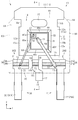
- FIG. 1 is a schematic perspective view showing the semiconductor device of the first embodiment.
- FIG. 2 is a schematic plan view of the semiconductor device of the first embodiment.
- FIG. 3 is a schematic back view of the semiconductor device of the first embodiment.
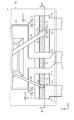
- FIG. 4 is a cross-sectional view taken along the line 4-4 of FIG.
- FIG. 5 is a schematic side view of the semiconductor device of the first embodiment.
- FIG. 6 is a partially enlarged plan view showing the semiconductor device of the first embodiment.
- FIG. 7 is a partially enlarged plan view showing the semiconductor device of the modified example of the first embodiment.
- FIG. 8 is a partially enlarged plan view showing the semiconductor device of the modified example of the first embodiment.
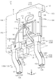
- FIG. 9 is a schematic perspective view showing the semiconductor device of the second embodiment.
- FIG. 10 is a schematic plan view of the semiconductor device of the second embodiment.
- FIG. 11 is a schematic back view of the semiconductor device of the second embodiment.
- FIG. 12 is a cross-sectional view taken along the line 12-12 of FIG.
- FIG. 13 is a schematic side view of the semiconductor device of the second embodiment.
- FIG. 14 is a schematic side view of the semiconductor device of the second embodiment.
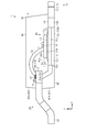
- FIG. 15 is a cross-sectional photograph showing the drive pad and the sealing resin.
- the semiconductor device 1 includes a substrate 10, a drive lead 20, a control lead 30, a semiconductor element 40, a drive wire 50, a control wire 60, and a sealing resin 80.
- the sealing resin 80 seals the semiconductor element 40, the control wire 60, and the drive wire 50.
- the sealing resin 80 is formed so as to expose a part of the substrate 10, the drive lead 20, and the control lead 30.
- the drive lead 20 has an outer lead 20A protruding from the sealing resin 80 and an inner lead 20B provided in the sealing resin 80 and electrically connected to the outer lead 20A.
- the outer lead 20A and the inner lead 20B are an integrated single component.
- the control lead 30 has an outer lead 30A protruding from the sealing resin 80 and an inner lead 30B provided in the sealing resin 80 and electrically connected to the outer lead 30A.
- the outer lead 30A and the inner lead 30B are an integrated single component.
- the semiconductor device 1 of this embodiment is a TO (Transistor Outline) -252 package defined in the package outline standard (JEITA standard). Further, the semiconductor device 1 is a so-called SIP (Single Inline Package) type in which the outer lead 20A of the drive lead 20 and the outer lead 30A of the control lead 30 extend from one surface of the sealing resin 80, respectively.
- the shape of the sealing resin 80 is a rectangular parallelepiped.
- the sealing resin 80 is shown by a chain double-dashed line, and the parts inside the sealing resin 80 are shown by a solid line.
- the sealing resin 80 is a synthetic resin having electrical insulation.
- the sealing resin 80 is an epoxy resin.
- the sealing resin 80 includes a first sealing resin side surface 81, a second sealing resin side surface 82, a third sealing resin side surface 83, a fourth sealing resin side surface 84, a sealing resin back surface 85, and a sealing resin top surface. It has 6 faces of 86.
- the first sealing resin side surface 81 and the second sealing resin side surface 82 face each other at intervals.
- the third sealing resin side surface 83 and the fourth sealing resin side surface 84 face each other at intervals.
- the sealing resin back surface 85 and the sealing resin top surface 86 face each other at intervals.
- the direction in which the sealing resin back surface 85 and the sealing resin top surface 86 are arranged is the thickness direction Z, and the first sealing resin side surface 81 and the second sealing resin side surface 82 are arranged.
- the direction is the vertical direction X
- the direction in which the third sealing resin side surface 83 and the fourth sealing resin side surface 84 are arranged is the horizontal direction Y.
- the vertical direction X and the horizontal direction Y are directions orthogonal to the thickness direction Z.
- the vertical direction X is a direction orthogonal to the horizontal direction Y.
- the thickness direction Z corresponds to the first direction
- the vertical direction X corresponds to the second direction
- the horizontal direction Y corresponds to the third direction.
- the shape of the sealing resin 80 is a rectangular parallelepiped.
- the sealing resin 80 is a synthetic resin having electrical insulation.
- the sealing resin 80 is an epoxy resin.
- the sealing resin 80 includes a first sealing resin side surface 81, a second sealing resin side surface 82, a third sealing resin side surface 83, a fourth sealing resin side surface 84, a sealing resin back surface 85, and a sealing resin top surface. It has 6 faces of 86.
- the first sealing resin side surface 81 and the second sealing resin side surface 82 face each other at intervals.
- the third sealing resin side surface 83 and the fourth sealing resin side surface 84 face each other at intervals.
- the sealing resin back surface 85 and the sealing resin top surface 86 face each other at intervals.
- the direction in which the sealing resin back surface 85 and the sealing resin top surface 86 are arranged is the thickness direction Z, and the first sealing resin side surface 81 and the second sealing resin side surface 82 are arranged.
- the direction is the vertical direction X
- the direction in which the third sealing resin side surface 83 and the fourth sealing resin side surface 84 are arranged is the horizontal direction Y.
- the vertical direction X and the horizontal direction Y are directions orthogonal to the thickness direction Z.
- the vertical direction X is a direction orthogonal to the horizontal direction Y.
- the vertical direction X corresponds to the first direction
- the horizontal direction Y corresponds to the second direction.
- FIG. 2 is a view of the semiconductor device 1 as viewed from the top surface 86 of the sealing resin in the thickness direction Z.
- the shape of the sealing resin 80 is such that the vertical direction X is the long side direction and the horizontal direction Y is the short side direction. It has a substantially rectangular shape. Viewing from the thickness direction Z is hereinafter referred to as plan view.
- the first sealing resin side surface 81 and the second sealing resin side surface 82 are side surfaces along the horizontal direction Y
- the third sealing resin side surface 83 and the fourth sealing resin side surface 84 are along the vertical direction X. The side.
- the substrate 10 has a main surface 10a and a back surface 10b (see FIG. 3) facing opposite sides in the thickness direction Z.
- the main surface 10a faces the same direction as the sealing resin top surface 86
- the back surface 10b faces the same direction as the sealing resin back surface 85.
- the substrate 10 is made of, for example, Cu (copper).
- the term "composed of Cu” means that it is made of Cu or an alloy containing Cu.
- the substrate 10 has a flat plate-shaped substrate main body portion 11 and a lead portion 16. In the present embodiment, the substrate main body portion 11 and the lead portion 16 are integrated into a single component.
- the substrate main body 11 can be divided into an inner main body 12 covered with the sealing resin 80 and a protruding portion 13 protruding from the sealing resin 80.
- the inner main body portion 12 and the protruding portion 13 are adjacent to each other in the vertical direction X.
- the protruding portion 13 projects from the side surface 81 of the first sealing resin in the vertical direction X.
- the size of the protruding portion 13 in the lateral direction Y is smaller than the size of the inner main body portion 12 in the lateral direction Y.
- the size of the protruding portion 13 in the lateral direction Y can be arbitrarily changed. In one example, the size of the protruding portion 13 in the lateral direction Y may be equal to the size of the inner main body portion 12 in the lateral direction Y.
- the inner main body portion 12 is arranged so that the center of the inner main body portion 12 is closer to the side surface 81 of the first sealing resin than the center of the sealing resin 80 in the vertical direction X.
- the inner main body portion 12 has a main surface 12a, a back surface 12b (see FIG. 3), a first side surface 12c, a second side surface 12d, and a third side surface 12e.
- the main surface 12a and the back surface 12b face each other in the thickness direction Z.
- the main surface 12a constitutes a part of the main surface 10a of the substrate 10
- the back surface 12b constitutes the back surface 10b of the substrate 10.
- the main surface 12a faces the sealing resin top surface 86 side
- the back surface 12b faces the sealing resin back surface 85 side.
- the first side surface 12c faces the second sealing resin side surface 82
- the second side surface 12d faces the third sealing resin side surface 83
- the third side surface 12e faces the fourth sealing resin side surface 84.
- the first side surface 12c extends along the lateral direction Y.
- the second side surface 12d and the third side surface 12e face each other with a gap in the lateral direction Y.
- the second side surface 12d and the third side surface 12e extend along the vertical direction X.
- a narrow portion 14 is formed at the end of the inner main body portion 12 on the protruding portion 13 side.
- the narrow portion 14 has a recess 14a recessed from the second side surface 12d toward the fourth sealing resin side surface 84 side in the lateral direction Y, and the narrow portion 14 toward the third sealing resin side surface 83 side in the lateral direction Y from the third side surface 12e. It is formed by a recess 14b that is recessed.
- the size of the narrow portion 14 in the lateral direction Y is smaller than the size of the portion of the inner main body portion 12 other than the narrow portion 14 in the lateral direction. Further, the size of the narrow portion 14 in the lateral direction Y is smaller than the size of the protruding portion 13 in the lateral direction Y.
- the narrow portion 14 is provided so as to be adjacent to the first sealing resin side surface 81 of the sealing resin 80 in the vertical direction X.
- the narrow portion 14 is provided with a through hole 15 penetrating the narrow portion 14 in the thickness direction Z.
- the shape of the through hole 15 in a plan view is an ellipse in which the lateral direction Y is the longitudinal direction.
- the inner main body portion 12 has flange portions 19a and 19b protruding from the main body side surface of the inner main body portion 12.
- the flange portion 19a projects from the second side surface 12d of the inner main body portion 12 toward the third sealing resin side surface 83.
- the flange portion 19b projects from the third side surface 12e of the inner main body portion 12 toward the fourth sealing resin side surface 84.
- the flange portions 19a and 19b are provided so as to be flush with the main surface 12a of the inner main body portion 12, respectively. Therefore, the main surface 10a of the substrate 10 is composed of the main surface 12a of the inner main body portion 12 and the flange portions 19a and 19b. Further, the flange portions 19a and 19b are provided so as to be on the main surface 12a side of the back surface 12b of the inner main body portion 12, respectively. Therefore, the back surface 10b of the substrate 10 is composed of the back surface 12b of the inner main body 12.
- the flange portions 19a and 19b suppress the separation of the substrate 10 and the sealing resin 80.
- the back surface 10b of the substrate 10 (the back surface 12b of the inner main body 12) is exposed from the back surface 85 of the sealing resin.
- the sealing resin 80 has entered the recesses 14a and 14b and the through holes 15 of the narrow portion 14 of the inner main body portion 12. As a result, the separation between the substrate 10 and the sealing resin 80 can be further suppressed.
- the lead portion 16 extends from the end portion of the inner main body portion 12 on the first side surface 12c side toward the second sealing resin side surface 82 and the second sealing resin side surface 82. Protruding from.
- the lead portion 16 can be divided into a terminal portion 17 protruding from the side surface 82 of the second sealing resin and a connecting portion 18 connecting the terminal portion 17 and the inner main body portion 12.
- the connecting portion 18 is located on the second side surface 12d side of the central portion of the inner main body portion 12 in the lateral direction Y.
- the connecting portion 18 is continuous from the flange portion 19a. That is, the thickness of the portion of the connecting portion 18 connected to the inner main body portion 12 is thicker than the thickness of the flange portions 19a and 19b and thinner than the thickness of the inner main body portion 12.
- the connecting portion 18 has an inclined portion 18a.
- the inclined portion 18a is inclined toward the sealing resin top surface 86 from the first side surface 12c of the inner main body portion 12 toward the second sealing resin side surface 82.
- the intermediate portion 18b between the inclined portion 18a and the terminal portion 17 of the connecting portion 18 is located on the sealing resin top surface 86 side of the main surface 12a of the inner main body portion 12.
- the intermediate portion 18b has a bent portion 18c that bends toward the side surface 84 of the fourth sealing resin.
- the portion of the intermediate portion 18b that comes into contact with the second sealing resin side surface 82 is located at the central portion of the second sealing resin side surface 82 in the lateral direction Y.
- the terminal portion 17 protrudes from the central portion of the second sealing resin side surface 82 in the lateral direction Y. In the thickness direction Z, the position of the terminal portion 17 is the same as the position of the intermediate portion 18b. That is, the terminal portion 17 is located on the sealing resin top surface 86 side of the main surface 12a of the inner main body portion 12.
- the drive lead 20 and the control lead 30 are separated from the substrate 10 in the vertical direction X on the second sealing resin side surface 82 side of the sealing resin 80. It is arranged in the state.
- the drive lead 20 and the control lead 30 are arranged so as to be separated from each other in the lateral direction Y.
- a lead portion 16 is arranged between the drive lead 20 and the control lead 30 in the lateral direction Y.
- the drive lead 20 has a drive pad 21, a drive terminal 22, and a connecting portion 23 that connects the drive pad 21 and the drive terminal 22.
- the drive pad 21 and the connecting portion 23 form an inner lead 20B, and the drive terminal 22 constitutes an outer lead 20A.
- the drive pad 21 and the connecting portion 23 are arranged between the substrate 10 and the second sealing resin side surface 82 in the vertical direction X.
- the drive pad 21 and the connecting portion 23 are arranged on the side surface 84 side of the fourth sealing resin in the lateral direction Y with respect to the central portion of the sealing resin 80 in the lateral direction Y.
- the drive lead 20 is made of Cu in this embodiment. That is, the drive lead 20 is made of the same material as the substrate 10.
- the shape of the drive pad 21 in a plan view is a rectangular shape in which the horizontal direction Y is the long side direction and the vertical direction X is the short side direction.
- the drive pad 21 has a first end portion 21a and a second end portion 21b which are both end portions in the lateral direction Y.
- the drive pad 21 is located on the sealing resin top surface 86 side of the main surface 12a of the inner main body portion 12 in the thickness direction Z. Further, the drive pad 21 is located on the sealing resin top surface 86 side of the main surface 40a of the semiconductor element 40 in the thickness direction Z.
- the drive pad 21 is at the same position as the intermediate portion 18b of the lead portion 16 in the thickness direction Z.
- the connecting portion 23 is continuous from the end portion of the drive pad 21 on the side surface 82 side of the second sealing resin.
- the connecting portion 23 is located on the side surface 84 side of the fourth sealing resin with respect to the central portion of the drive pad 21 in the lateral direction Y.
- the drive terminal 22 constitutes a source terminal. As shown in FIG. 5, the drive terminal 22 projects from the first inclined surface 82a of the second sealing resin side surface 82.
- the control lead 30 has a control pad 31, a control terminal 32, and a connecting portion 33 that connects the control pad 31 and the control terminal 32.
- the control pad 31 and the connecting portion 33 form an inner lead 30B, and the control terminal 32 constitutes an outer lead 30A.
- the control pad 31 and the connecting portion 33 are arranged between the substrate 10 and the second sealing resin side surface 82 in the vertical direction X.
- the control pad 31 and the connecting portion 33 are arranged on the side surface 83 side of the third sealing resin 80 with respect to the central portion of the sealing resin 80 in the lateral direction Y.
- the control lead 30 is made of Cu in this embodiment. That is, the control lead 30 is made of the same material as the substrate 10 and the drive lead 20.
- the shape of the control pad 31 in a plan view is a substantially rectangular shape in which the horizontal direction Y is the long side direction and the vertical direction X is the short side direction.
- the control pad 31 has a first end portion 31a and a second end portion 31b which are both end portions in the lateral direction Y.
- the size of the control pad 31 in the lateral direction Y is smaller than the size of the drive pad 21 in the lateral direction Y.
- the control pad 31 is located on the sealing resin top surface 86 side of the main surface 12a of the inner main body portion 12 in the thickness direction Z. Further, the control pad 31 is located on the sealing resin top surface 86 side of the main surface 40a of the semiconductor element 40 in the thickness direction Z. In the present embodiment, the control pad 31 is at the same position as the intermediate portion 18b of the lead portion 16 in the thickness direction Z.
- the connecting portion 33 is continuous from the end portion of the control pad 31 on the side surface 82 side of the second sealing resin.
- the connecting portion 33 is located closer to the third sealing resin side surface 83 of the control pad 31 in the lateral direction Y.
- the control terminal 32 constitutes a gate terminal.
- the control terminal 32 projects from the first inclined surface 82a of the second sealing resin side surface 82.
- the drive pad 21 has a connecting surface 24 facing the same direction as the main surface 10a of the substrate 10.
- a plating layer 71 is formed on the connection surface 24 to cover a part of the connection surface 24.
- the plating layer 71 is made of, for example, Ni (nickel). By being composed of Ni, it is intended that it is formed of Ni or an alloy containing Ni.
- the plating layer 71 is formed in the center of the drive pad 21 in the short side direction and the vertical direction X of the drive pad 21. Further, the plating layer 71 extends from the first end portion 21a to the second end portion 21b of the drive pad 21 along the long side direction of the drive pad 21, that is, the lateral direction Y. Therefore, the connection surface 24 of the drive pad 21 has a portion 24a covered with the plating layer 71 and a portion 24b exposed from the plating layer 71.
- the control pad 31 has a connecting surface 34 facing the same direction as the main surface 10a of the substrate 10.
- a plating layer 72 that covers a part of the connection surface 34 is formed on the connection surface 34.
- the plating layer 72 is made of, for example, Ni. By being composed of Ni, it is intended that it is formed of Ni or an alloy containing Ni.
- the plating layer 72 is formed in the center of the control pad 31 in the short side direction and the vertical direction X of the control pad 31. Further, the plating layer 72 extends from the first end portion 31a to the second end portion 31b of the control pad 31 along the long side direction of the control pad 31, that is, the lateral direction Y. Therefore, the connection surface 34 of the control pad 31 has a portion 34a covered with the plating layer 72 and a portion 34b exposed from the plating layer 72.
- the plating layer 71 formed on the drive pad 21 and the plating layer 72 formed on the control pad 31 are at the same position in the vertical direction X. Further, in the vertical direction X, the width W71 of the plating layer 71 formed on the drive pad 21 is equal to the width W72 of the plating layer 72 formed on the control pad 31. Therefore, the plating layer 71 formed on the drive pad 21 and the plating layer 72 formed on the control pad 31 overlap each other when viewed from the lateral direction Y.
- the end portion on the inclined portion 18a side is located at the same height as the drive pad 21 and the control pad 31.
- the plating layers 71 and 72 are formed, for example, on the upper surface of the intermediate portion 18b, a plating layer 73 that overlaps with the plating layers 71 and 72 when viewed from the lateral direction Y.
- the semiconductor element 40 is mounted on the main surface 12a of the inner main body portion 12 by solder SD. As shown in FIG. 2, in the present embodiment, the semiconductor element 40 is arranged in the central portion of the inner main body portion 12. Further, the semiconductor element 40 and the drive pad 21 are displaced in the vertical direction X. Further, the semiconductor element 40 and the control pad 31 are displaced in the vertical direction X.
- the semiconductor element 40 is a silicon carbide (SiC) chip.
- SiC MOSFET metal-oxide-semiconductor field-effect transistor
- the semiconductor element 40 SiCMOSFT is an element capable of high-speed switching.
- the switching frequency is, for example, 1 kHz or more and several hundred kHz or less.
- the semiconductor element 40 is formed in a flat plate shape. Specifically, in a plan view, the shape of the semiconductor element 40 is, for example, a square shape. As shown in FIGS. 2 and 4, the semiconductor element 40 has a main surface 40a, a back surface 40b, and a plurality of side surfaces 40c to 40f. The main surface 40a and the back surface 40b face each other in the thickness direction Z.
- the main surface 40a faces the sealing resin top surface 86. That is, the main surface 40a faces the same direction as the main surface 10a of the substrate 10.
- the back surface 40b faces the back surface 85 of the sealing resin.
- the back surface 40b faces the main surface 12a of the inner main body 12.
- the side surface 40c faces the first sealing resin side surface 81
- the side surface 40d faces the second sealing resin side surface 82
- the side surface 40e faces the third sealing resin side surface 83
- the side surface 40f faces the fourth sealing resin side surface. It faces the side surface 84.
- a main surface side drive electrode 41 and a control electrode 43 are formed on the main surface 40a.
- the main surface side drive electrode 41 and the control electrode 43 form a main surface electrode formed on the main surface 40a of the semiconductor element 40.
- a back surface side drive electrode 42 (see FIG. 4) is formed on the back surface 40b.
- the main surface side drive electrode 41 constitutes the source electrode
- the back surface side drive electrode 42 constitutes the drain electrode.
- the control electrode 43 constitutes a gate electrode.
- the back surface side drive electrode 42 is electrically connected to the inner main body portion 12 by a solder SD.
- the solder SD is, for example, lead solder.
- the semiconductor element 40 has a passivation film formed on the main surface 40a.
- the passivation film is formed with an opening that exposes the electrodes on the main surface 40a side of the semiconductor element 40 as the main surface side drive electrodes 41 and the control electrodes 43.
- the semiconductor device 1 includes one drive wire 50 and one control wire 60.
- the drive wire 50 and the control wire 60 are made of the same metal.
- the drive wire 50 and the control wire 60 are made of Al (aluminum). By being composed of Al, it is intended that it is formed of Al or an alloy containing Al.
- the drive wire 50 has a circular cross-sectional shape perpendicular to the major axis direction near the center.
- the control wire 60 has a circular cross-sectional shape perpendicular to the major axis direction near the center.
- the wire diameter of the drive wire 50 is larger than the wire diameter of the control wire 60. That is, the drive wire 50 is a large-diameter aluminum wire.
- the wire diameter of the drive wire 50 is, for example, 200 ⁇ m or more and 600 ⁇ m or less.
- the wire diameter of the control wire 60 is, for example, 40 ⁇ m or more and 100 ⁇ m or less.
- the first end 51 of the drive wire 50 is joined to the main surface side drive electrode 41 of the semiconductor element 40, and the second end 52 of the drive wire 50 is formed on a plating layer 71 that covers a part of the connection surface 24 of the drive pad 21. It is joined.
- the drive wire 50 is bonded to the main surface side drive electrode 41 and the drive pad 21 by, for example, ultrasonic bonding.
- the joint portion 53 of the second end 52 of the drive wire 50 is a portion 53a joined to the upper surface of the plating layer 71 and a portion 24b exposed from the plating layer 71 of the connection surface 24 of the drive pad 21. It has a portion 53b joined to. As shown in FIG.
- the area of the portion 53a of the upper surface of the plating layer 71 where the second end 52 of the drive wire 50 and the plating layer 71 are joined is a cross section perpendicular to the long axis direction of the drive wire 50. It is more than the area. That is, the width W71 in the vertical direction X of the plating layer 71 is set so that the bonding area between the plating layer 71 and the drive wire 50 bonded to the plating layer 71 is equal to or larger than the cross-sectional area of the drive wire 50.
- the joining portion 53 shows an example having the portion 53a and the portion 53b, but the width W71 of the plating layer 71 is set so that all the joining portions 53 are joined to the plating layer 71. You may.
- the first end 61 of the control wire 60 is joined to the control electrode 43 of the semiconductor element 40, and the second end 62 of the control wire 60 is one of the connection surfaces 34 of the control pad 31. It is joined to the plating layer 72 that covers the portion.
- the control wire 60 is bonded to the control electrode 43 and the control pad 31 by, for example, ultrasonic bonding.
- the joint portion 63 of the second end 62 of the control wire 60 is joined only to the upper surface of the plating layer 72. That is, the plating layer 72 is set to have a width W72 in the vertical direction X so that the joint portion 63 of the second end 62 of the control wire 60 to be joined does not protrude.
- the semiconductor element 40 is mounted on the main surface 10a of the substrate 10, and the connection surfaces 24 and 34 of the drive pad 21 and the control pad 31 made of Cu are made of Ni and are made of Ni.
- Plating layers 71 and 72 that cover a part of 34 are formed.
- the first end 51 of the drive wire 50 made of Al is joined to the main surface side drive electrode 41 of the semiconductor element 40, and the second end 52 of the drive wire 50 is the plating layer 71 on the connection surface 24 of the drive pad 21. It is joined to.
- the first end 61 of the control wire 60 made of Al is bonded to the control electrode 43 of the semiconductor element 40, and the second end 62 of the control wire 60 is bonded to the plating layer 72 on the connection surface 34 of the control pad 31. ing.
- the semiconductor element 40, the drive pad 21, the control pad 31, the plating layers 71 and 72, the drive wire 50, and the control wire 60 are sealed with the sealing resin 80.
- the connection surface 24 of the drive pad 21 has a portion 24a covered with the plating layer 71 and a portion 24b exposed from the plating layer 71.
- the plating layer 71 made of Ni prevents the drive wire 50 from separating from the drive pad 21.
- the drive wire 50 made of Al is directly bonded to the drive pad 21 made of Cu, the intermetallic compound held between the drive wire 50 and the drive pad 21 grows due to heat, and the drive wire 50 is driven.
- the pad 21 may be separated from the pad 21. Therefore, the plating layer 71 made of Ni prevents the formation of intermetallic compounds and prevents the drive wire 50 from separating from the drive pad 21.
- the portion 24b exposed from the plating layer 71 on the connection surface 24 of the drive pad 21 is the surface of the drive pad 21 made of Cu, and has good adhesion to the sealing resin 80. Therefore, this portion 24b suppresses the peeling of the sealing resin 80 from the drive pad 21.
- the sealing resin 80 is peeled from the drive pad 21, the drive wire 50 joined to the drive pad 21 may be broken due to the peeling. Therefore, the portion 24b exposed from the plating layer 71 suppresses the peeling of the sealing resin 80 from the drive pad 21, and suppresses the disconnection of the drive wire 50.
- the connection surface 34 of the control pad 31 has a portion 34a covered with the plating layer 72 and a portion 34b exposed from the plating layer 72.
- the plating layer 72 made of Ni prevents the control wire 60 from being separated from the control pad 31.
- the control wire 60 made of Al is directly bonded to the control pad 31 made of Cu, the intermetallic compound held between the control wire 60 and the control pad 31 grows due to heat, and the control wire 60 controls the control wire 60.
- the pad 31 may be separated from the pad 31. Therefore, the plating layer 72 made of Ni prevents the formation of intermetallic compounds and prevents the control wire 60 from separating from the control pad 31.
- the portion 34b exposed from the plating layer 72 on the connection surface 34 of the control pad 31 is the surface of the control pad 31 made of Cu, and has good adhesion to the sealing resin 80. Therefore, this portion 34b suppresses the peeling of the sealing resin 80 from the control pad 31.
- the portion 34b exposed from the plating layer 72 suppresses the peeling of the sealing resin 80 from the control pad 31, and suppresses the disconnection of the control wire 60.
- a large-diameter drive wire 50 made of Al is used between the main surface side drive electrode 41 of the semiconductor element 40 and the drive pad 21. ing.
- a wire such as Au (gold) or Cu
- a plurality of wires must be connected according to the current, which leads to an increase in man-hours for connection and an increase in pad area, that is, an increase in the size of the semiconductor device.
- a required current can be passed by one drive wire 50, and an increase in man-hours and an increase in size can be suppressed.
- the semiconductor element 40 is mounted on the main surface 10a of the substrate 10, and the connection surfaces 24 and 34 of the drive pad 21 made of Cu and the control pad 31 are made of Ni and cover a part of the connection surfaces 24 and 34.
- Plating layers 71 and 72 are formed.
- the first end 51 of the drive wire 50 made of Al is joined to the main surface side drive electrode 41 of the semiconductor element 40, and the second end 52 of the drive wire 50 is the plating layer 71 on the connection surface 24 of the drive pad 21. It is joined to.
- the first end 61 of the control wire 60 made of Al is bonded to the control electrode 43 of the semiconductor element 40, and the second end 62 of the control wire 60 is bonded to the plating layer 72 on the connection surface 34 of the control pad 31. ing.
- the semiconductor element 40, the drive pad 21, the control pad 31, the plating layers 71 and 72, the drive wire 50, and the control wire 60 are sealed with the sealing resin 80.
- the plating layer 72 made of Ni can prevent the control wire 60 from being separated from the control pad 31.
- the portion 24b exposed from the plating layer 71 on the connection surface 24 of the drive pad 21 has good adhesion to the sealing resin 80, suppresses peeling of the sealing resin 80 from the drive pad 21, and suppresses disconnection of the drive wire 50. can.
- the plating layer 71 made of Ni can prevent the drive wire 50 from being separated from the drive pad 21.
- the portion 24b exposed from the plating layer 71 on the connection surface 34 of the drive pad 21 has good adhesion to the sealing resin 80, suppresses peeling of the sealing resin 80 from the drive pad 21, and suppresses disconnection of the drive wire 50. can.
- the semiconductor device 101 includes a substrate 110, a drive lead 120, a control lead 130, a semiconductor element 140, a drive wire 150, a control wire 160, and a sealing resin 180.
- the sealing resin 180 seals the semiconductor element 140, the control wire 160, and the drive wire 150.
- the sealing resin 180 is formed so as to expose a part of the substrate 110, the drive lead 120, and the control lead 130.
- the drive lead 120 has an outer lead 120A protruding from the sealing resin 180 and an inner lead 120B provided in the sealing resin 180 and electrically connected to the outer lead 120A.
- the outer lead 120A and the inner lead 120B are an integrated single component.
- the control lead 130 has an outer lead 130A protruding from the sealing resin 180, and an inner lead 130B provided in the sealing resin 180 and electrically connected to the outer lead 130A.
- the outer lead 130A and the inner lead 130B are an integrated single component.
- the semiconductor device 101 of this embodiment is a TO (Transistor Outline) -252 package defined in the package outline standard (JEITA standard). Further, the semiconductor device 101 is a so-called SIP (Single Inline Package) type in which the outer lead 120A of the drive lead 120 and the outer lead 130A of the control lead 130 extend from one surface of the sealing resin 180, respectively.
- the shape of the sealing resin 180 is a rectangular parallelepiped.
- the sealing resin 180 is indicated by a chain double-dashed line, and the parts inside the sealing resin 180 are indicated by a solid line.
- the sealing resin 180 is a synthetic resin having electrical insulation.
- the sealing resin 180 is an epoxy resin.
- the sealing resin 180 includes a first sealing resin side surface 181, a second sealing resin side surface 182, a third sealing resin side surface 83, a fourth sealing resin side surface 184, a sealing resin back surface 185, and a sealing resin top surface. It has 6 faces of 186.
- the first sealing resin side surface 181 and the second sealing resin side surface 182 face each other at intervals.
- the third sealing resin side surface 83 and the fourth sealing resin side surface 184 face each other at intervals.
- the sealing resin back surface 185 and the sealing resin top surface 186 face each other at intervals.
- the direction in which the sealing resin back surface 185 and the sealing resin top surface 186 are arranged is defined as the thickness direction Z, and the first sealing resin side surface 181 and the second sealing resin side surface 182 are arranged.
- the direction is the vertical direction X
- the direction in which the third sealing resin side surface 83 and the fourth sealing resin side surface 184 are arranged is the horizontal direction Y.
- the vertical direction X and the horizontal direction Y are directions orthogonal to the thickness direction Z.
- the vertical direction X is a direction orthogonal to the horizontal direction Y.
- the thickness direction Z corresponds to the first direction
- the vertical direction X corresponds to the second direction
- the horizontal direction Y corresponds to the third direction.
- the shape of the sealing resin 180 is a rectangular parallelepiped.
- the sealing resin 180 is a synthetic resin having electrical insulation.
- the sealing resin 180 is an epoxy resin.
- the sealing resin 180 includes a first sealing resin side surface 181, a second sealing resin side surface 182, a third sealing resin side surface 83, a fourth sealing resin side surface 184, a sealing resin back surface 185, and a sealing resin top surface. It has 6 faces of 186.
- the first sealing resin side surface 181 and the second sealing resin side surface 182 face each other at intervals.
- the third sealing resin side surface 83 and the fourth sealing resin side surface 184 face each other at intervals.
- the sealing resin back surface 185 and the sealing resin top surface 186 face each other at intervals.
- the direction in which the sealing resin back surface 185 and the sealing resin top surface 186 are arranged is defined as the thickness direction Z, and the first sealing resin side surface 181 and the second sealing resin side surface 182 are arranged.
- the direction is the vertical direction X
- the direction in which the third sealing resin side surface 83 and the fourth sealing resin side surface 184 are arranged is the horizontal direction Y.
- the vertical direction X and the horizontal direction Y are directions orthogonal to the thickness direction Z.
- the vertical direction X is a direction orthogonal to the horizontal direction Y.
- the vertical direction X corresponds to the first direction
- the horizontal direction Y corresponds to the second direction.
- FIG. 10 is a view of the semiconductor device 101 as viewed from the top surface 186 of the sealing resin in the thickness direction Z.
- the shape of the sealing resin 180 is such that the vertical direction X is the long side direction and the horizontal direction Y is the short side direction. It has a substantially rectangular shape. Viewing from the thickness direction Z is hereinafter referred to as plan view.
- the first sealing resin side surface 181 and the second sealing resin side surface 182 are side surfaces along the horizontal direction Y
- the third sealing resin side surface 83 and the fourth sealing resin side surface 184 are along the vertical direction X. The side.
- the substrate 110 has a main surface 110a and a back surface 110b (see FIG. 11) facing opposite sides in the thickness direction Z.
- the main surface 110a faces the same direction as the sealing resin top surface 186
- the back surface 110b faces the same direction as the sealing resin back surface 185.
- the substrate 110 has a flat plate-shaped substrate main body 111 and a lead 116. In the present embodiment, the substrate main body 111 and the lead 116 are integrated as a single component.
- the substrate main body 111 is a die bonding pad on which the semiconductor element 140 is mounted.
- the substrate main body 111 can be divided into an inner main body 112 covered with the sealing resin 180 and a protruding portion 113 protruding from the sealing resin 180.
- the inner main body portion 112 and the protruding portion 113 are adjacent to each other in the vertical direction X.
- the protruding portion 113 protrudes from the side surface 181 of the first sealing resin in the vertical direction X.
- the size of the protruding portion 113 in the lateral direction Y is smaller than the size of the inner main body portion 112 in the lateral direction Y.
- the size of the protruding portion 113 in the lateral direction Y can be arbitrarily changed. In one example, the size of the protruding portion 113 in the lateral direction Y may be equal to the size of the inner main body portion 112 in the lateral direction Y.
- the inner main body portion 112 is arranged so that the center of the inner main body portion 112 is closer to the side surface 181 of the first sealing resin than the center of the sealing resin 180 in the vertical direction X.
- the inner main body portion 112 has a main surface 112a, a back surface 112b (see FIG. 11), a first side surface 112c, a second side surface 112d, and a third side surface 112e.
- the main surface 112a and the back surface 112b face each other in the thickness direction Z.
- the main surface 112a constitutes a part of the main surface 110a of the substrate 110
- the back surface 112b constitutes the back surface 110b of the substrate 110.
- the main surface 112a faces the sealing resin top surface 186 side
- the back surface 112b faces the sealing resin back surface 185 side
- the first side surface 112c faces the second sealing resin side surface 182
- the second side surface 112d faces the third sealing resin side surface 83
- the third side surface 112e faces the fourth sealing resin side surface 184.
- the first side surface 112c extends along the lateral direction Y.
- the second side surface 112d and the third side surface 112e face each other with a gap in the lateral direction Y.
- the second side surface 112d and the third side surface 112e extend along the vertical direction X.
- a narrow portion 114 is formed at the end of the inner main body portion 112 on the protruding portion 113 side.
- the narrow portion 114 has a recess 114a recessed from the second side surface 112d toward the fourth sealing resin side surface 184 side in the lateral direction Y, and the narrow portion 114 toward the third sealing resin side surface 83 side in the lateral direction Y from the third side surface 112e. It is formed by a recess 114b that is recessed.
- the size of the narrow portion 114 in the lateral direction Y is smaller than the size of the portion of the inner main body portion 112 other than the narrow portion 114 in the lateral direction.
- the size of the narrow portion 114 in the lateral direction Y is smaller than the size of the protruding portion 113 in the lateral direction Y.
- the narrow portion 114 is provided so as to be adjacent to the first sealing resin side surface 181 of the sealing resin 180 in the vertical direction X.
- the narrow portion 114 is provided with a through hole 115 penetrating the narrow portion 114 in the thickness direction Z.
- the shape of the through hole 115 in a plan view is an ellipse in which the lateral direction Y is the longitudinal direction.
- the inner main body 112 has flanges 119a and 119b protruding from the side surface of the inner main body 112.
- the flange portion 119a projects from the second side surface 112d of the inner main body portion 112 toward the third sealing resin side surface 83.
- the flange portion 119b projects from the third side surface 112e of the inner main body portion 112 toward the fourth sealing resin side surface 184.
- the flange portions 119a and 119b are provided so as to be flush with the main surface 112a of the inner main body portion 112, respectively. Therefore, the main surface 110a of the substrate 110 is composed of the main surface 112a of the inner main body portion 112 and the flange portions 119a and 119b. Further, the flange portions 119a and 119b are provided so as to be closer to the main surface 112a than the back surface 112b of the inner main body portion 112, respectively. Therefore, the back surface 110b of the substrate 110 is composed of the back surface 112b of the inner main body 112.
- the flange portions 119a and 119b suppress the separation of the substrate 110 and the sealing resin 180.
- the back surface 110b of the substrate 110 (the back surface 112b of the inner main body 112) is exposed from the back surface 185 of the sealing resin.
- the sealing resin 180 has entered the recesses 114a and 114b and the through holes 115 of the narrow portion 114 of the inner main body 112, respectively. As a result, the separation between the substrate 110 and the sealing resin 180 can be further suppressed.
- the lead portion 116 extends from the end of the inner main body portion 112 on the first side surface 112c side toward the second sealing resin side surface 182 and the second sealing resin side surface 182. Protruding from.
- the lead portion 116 can be divided into a terminal portion 117 protruding from the side surface 182 of the second sealing resin and a connecting portion 118 connecting the terminal portion 117 and the inner main body portion 112.
- the connecting portion 118 is located on the second side surface 112d side of the central portion of the inner main body portion 112 in the lateral direction Y.
- the connecting portion 118 is continuous from the flange portion 119a. That is, the thickness of the portion of the connecting portion 118 connected to the inner main body portion 112 is thicker than the thickness of the flange portions 119a and 119b and thinner than the thickness of the inner main body portion 112.
- the connecting portion 118 has an inclined portion 118a.
- the inclined portion 118a is inclined toward the sealing resin top surface 186 from the first side surface 112c of the inner main body portion 112 toward the second sealing resin side surface 182.
- the intermediate portion 118b between the inclined portion 118a and the terminal portion 117 of the connecting portion 118 is located on the sealing resin top surface 186 side of the main surface 112a of the inner main body portion 112.
- the intermediate portion 118b has a bent portion 118c that bends toward the side surface 184 of the fourth sealing resin.
- the portion of the intermediate portion 118b that comes into contact with the second sealing resin side surface 182 is located at the central portion of the second sealing resin side surface 182 in the lateral direction Y.
- the terminal portion 117 protrudes from the central portion of the second sealing resin side surface 182 in the lateral direction Y. In the thickness direction Z, the position of the terminal portion 117 is the same as the position of the intermediate portion 118b. That is, the terminal portion 117 is located on the sealing resin top surface 186 side of the main surface 112a of the inner main body portion 112.
- the drive lead 120 and the control lead 130 are separated from the substrate 110 in the vertical direction X on the second sealing resin side surface 182 side of the sealing resin 180. It is arranged in the state.
- the drive lead 120 and the control lead 130 are arranged so as to be separated from each other in the lateral direction Y.
- a lead portion 116 is arranged between the drive lead 120 and the control lead 130 in the lateral direction Y.
- the drive lead 120 has a drive pad 121, a drive terminal 122, and a connecting portion 1123 that connects the drive pad 121 and the drive terminal 122.
- the drive pad 121 and the connecting portion 1123 form an inner lead 120B, and the drive terminal 122 constitutes an outer lead 120A.
- the drive pad 121 and the connecting portion 1123 are arranged between the substrate 110 and the second sealing resin side surface 182 in the vertical direction X.
- the drive pad 121 and the connecting portion 1123 are arranged on the side surface 184 of the fourth sealing resin in the lateral direction Y with respect to the central portion of the sealing resin 180 in the lateral direction Y.
- the shape of the drive pad 121 in a plan view is a rectangular shape in which the horizontal direction Y is the long side direction and the vertical direction X is the short side direction.
- the drive pad 121 has an upper surface 121a, a lower surface 121b, and a plurality of side surfaces 121c.
- the upper surface 121a and the lower surface 121b face each other in the thickness direction Z.
- the upper surface 121a faces the same direction as the main surface 110a of the substrate 110.
- Each side surface 121c faces either the vertical direction X or the horizontal direction Y.
- the drive pad 121 is located on the sealing resin top surface 186 side of the main surface 112a of the inner main body portion 112 in the thickness direction Z. Further, the drive pad 121 is located on the sealing resin top surface 186 side of the main surface 140a of the semiconductor element 140 in the thickness direction Z. As shown in FIGS. 12 and 13, in the present embodiment, the drive pad 121 is at the same position as the intermediate portion 118b of the lead portion 116 in the thickness direction Z.
- the connecting portion 1123 is continuous from the end portion of the drive pad 121 on the side surface 182 of the second sealing resin.
- the connecting portion 1123 is located on the side surface 184 of the fourth sealing resin in the lateral direction Y with respect to the central portion of the drive pad 121.
- the drive terminal 122 constitutes a source terminal. As shown in FIG. 13, the drive terminal 122 protrudes from the first inclined surface 182a of the second sealing resin side surface 182.
- the control lead 130 has a control pad 131, a control terminal 132, and a connecting portion 1133 that connects the control pad 131 and the control terminal 132.
- the control pad 131 and the connecting portion 1133 form an inner lead 130B, and the control terminal 132 constitutes an outer lead 130A.
- the control pad 131 and the connecting portion 1133 are arranged between the substrate 110 and the second sealing resin side surface 182 in the vertical direction X.
- the control pad 131 and the connecting portion 1133 are arranged on the side surface 83 side of the third sealing resin 180 with respect to the central portion of the sealing resin 180 in the lateral direction Y.
- the shape of the control pad 131 in a plan view is a substantially rectangular shape in which the horizontal direction Y is the long side direction and the vertical direction X is the short side direction.
- the control pad 131 has an upper surface 131a, a lower surface 131b, and a plurality of side surfaces 131c.
- the upper surface 131a and the lower surface 131b face each other in the thickness direction Z.
- the upper surface 131a faces the same direction as the main surface 110a of the substrate 110.
- Each side surface 131c faces either the vertical direction X or the horizontal direction Y.
- the size of the control pad 131 in the lateral direction Y is smaller than the size of the drive pad 121 in the lateral direction Y.
- the control pad 131 is located on the sealing resin top surface 186 side of the main surface 112a of the inner main body portion 112 in the thickness direction Z. Further, the control pad 131 is located on the sealing resin top surface 186 side of the main surface 140a of the semiconductor element 140 in the thickness direction Z. In the present embodiment, the control pad 131 is at the same position as the intermediate portion 118b of the lead portion 116 in the thickness direction Z.
- the connecting portion 1133 is continuous from the end of the control pad 131 on the side surface 182 of the second sealing resin.
- the connecting portion 1133 is located closer to the third sealing resin side surface 83 of the control pad 131 in the lateral direction Y.
- the control terminal 132 constitutes a gate terminal.
- the control terminal 132 projects from the first inclined surface 182a of the second sealing resin side surface 182.
- the substrate 110 includes a first base material (board base material) 201 and a first plating layer (board plating layer) 202.
- the first base material 201 is made of Cu (copper). In the present embodiment, the term “composed of Cu” means that it is made of Cu or an alloy containing Cu.
- the first base material 201 is formed by using, for example, a metal plate formed by rolling.
- the first base material 201 has portions that serve as the above-mentioned flange portions 119a and 119b and lead portions 116 formed by pressing a metal plate.
- the first plating layer 202 is formed so as to cover the surface of the first base material 201.
- the first plating layer 202 is made of Ni (nickel). By being composed of Ni, it is intended that it is formed of Ni or an alloy containing Ni.
- the first base material 201 and the first plating layer 202 form each part of the substrate 110. That is, the first base material 201 includes a portion for forming the flat plate-shaped substrate main body portion 111 and a portion for forming the lead portion 116.
- the surface of the first plating layer 202 covering the first base material 201 forms the surface of the substrate 110, that is, each surface of the substrate main body 111 and each surface of the lead 116.
- the drive lead 120 includes a second base material 124 and a second plating layer 125.
- the second base material 124 has a pad portion 126 that forms the drive pad 121, and a lead portion 127 that forms the drive terminal 122 and the connecting portion 123.
- the pad portion 126 is formed in a rectangular parallelepiped shape.
- the pad portion 126 has an upper surface 126a, a lower surface 126b, and a plurality of side surfaces 126c.
- the upper surface 126a and the lower surface 126b face each other in the thickness direction Z.
- the upper surface 126a faces the same direction as the main surface 110a of the substrate 110.
- Each side surface 126c faces either the vertical direction X or the horizontal direction Y.
- the second plating layer 125 covers the surface of the pad portion 126, that is, covers the upper surface 126a, the lower surface 126b, and the side surface 126c of the pad portion 126. Therefore, the surfaces of the second plating layer 125 that covers the pad portion 126 are the upper surface 121a, the lower surface 121b, and the side surface 121c of the drive pad 121.
- the lead portion 127 extends from the pad portion 126 in the vertical direction X and protrudes from the sealing resin 180.
- the lead portion 127 has an upper surface 127a and a lower surface 127b facing opposite to each other in the thickness direction Z, a side surface 127c facing the lateral direction Y, and an end surface 127d facing the vertical direction X.
- the end surface 127d is the surface of the tip of the lead portion 127 protruding from the sealing resin 180.
- the second plating layer 125 is formed so as to cover the upper surface 127a, the lower surface 127b, and the side surface 127c of the lead portion 127. Therefore, the surface of the second plating layer 125 that covers the lead portion 127 is the surface of the drive terminal 122 and the connecting portion 123.
- the end face 127d that is, the end face 127d, which is the front end surface of the lead portion 127, is not covered by the second plating layer 125. That is, the end face 127d of the lead portion 127 is exposed from the second plating layer 125. In other words, the second base material 124 is exposed from the second plating layer 125 on the tip surface of the drive terminal 122.
- the second base material 124 is made of Cu. Like the first base material 201, the second base material 124 is formed by using, for example, a metal plate formed by rolling. The second base material 124 has a pad portion 126 and a lead portion 127 formed by pressing a metal plate.
- the second plating layer 125 is made of Ni. As shown in FIG. 15, the second plating layer 125 is a rough surface plating layer whose surface is rougher than the surface of the second base material 124.
- the second plating layer 125 which is a rough surface plating layer, can be obtained, for example, by subjecting the second base material 124 constituting the drive lead 120 to an electrolytic plating treatment.
- the control lead 130 includes a third base material 134 and a third plating layer 135.
- the third base material 134 has a pad portion 136 that forms the control pad 131, and a lead portion 137 that forms the control terminal 132 and the connecting portion 133.
- the pad portion 136 is formed in a rectangular parallelepiped shape.
- the pad portion 136 has an upper surface 127a, a lower surface 127b, and a plurality of side surfaces 127c.
- the upper surface 127a and the lower surface 127b face opposite to each other in the thickness direction.
- the upper surface 127a faces the same direction as the main surface 110a of the substrate 110.
- Each side surface 127c faces either the vertical direction X or the horizontal direction Y.
- the third plating layer 135 covers the surface of the pad portion 136, that is, covers the upper surface 136a, the lower surface 136b, and the side surface 136c of the pad portion 136. Therefore, the surfaces of the third plating layer 135 covering the pad portion 136 are the upper surface 131a, the lower surface 131b, and the side surface 131c of the control pad 131.
- the lead portion 137 extends from the pad portion 136 in the vertical direction X and protrudes from the sealing resin 180.
- the lead portion 137 has an upper surface 137a and a lower surface 137b facing opposite to each other in the thickness direction Z, a side surface 137c facing the lateral direction Y, and an end surface 137d facing the vertical direction X.
- the end surface 137d is the surface of the tip of the lead portion 137 protruding from the sealing resin 180.
- the third plating layer 135 is formed so as to cover the upper surface 137a, the lower surface 137b, and the side surface 137c of the lead portion 137. Therefore, the surface of the third plating layer 135 that covers the lead portion 137 is the surface of the control terminal 132 and the connecting portion 133.
- the end face 137d that is, the end face 137d, which is the front end surface of the lead portion 137, is not covered by the third plating layer 135. That is, the end face 137d of the lead portion 137 is exposed from the third plating layer 135. In other words, the third base material 134 is exposed from the third plating layer 135 on the tip surface of the control terminal 132.
- the third base material 134 is made of Cu. Like the first base material 201, the third base material 134 is formed by using, for example, a metal plate formed by rolling. The third base material 134 has a pad portion 136 and a lead portion 137 formed by pressing a metal plate.
- the third plating layer 135 is made of Ni. Like the second plating layer 125, the third plating layer 135 is a rough surface plating layer whose surface is rougher than the surface of the third base material 134.
- the third plating layer 135, which is a rough surface plating layer can be obtained, for example, by subjecting the third base material 134 constituting the control lead 130 to an electrolytic plating treatment.
- the first plating layer 202 constituting the substrate 110 has a rough surface that is rougher than the surface of the first base material 201 constituting the substrate 110, similarly to the second and third plating layers 125 and 135. It is a plating layer.
- the substrate 110, the drive lead 120, and the control lead 130 can be formed by using a lead frame.
- the lead frame including the substrate 110, the drive lead 120, and the control lead 130 can be formed by pressing the above metal plate.
- a first plating layer 202, a second plating layer 125, and a third plating layer 135, which are rough surface plating layers, are formed on the lead frame by, for example, an electrolytic plating method.
- the semiconductor device 101 is separated by cutting a predetermined portion of the lead frame.
- the second base material 124 and the third base material 134 are exposed at the end face 137d of the drive lead 120 and the end face 137d of the control lead 130.
- the first base material 201 is exposed at the cutting portion, for example, the surface of the protruding portion 113 toward the vertical direction X, as in the drive lead 120 and the control lead 130.
- the drive lead 120 and the control lead 130 have protrusions 1120T and 130T on the side surfaces.
- the protruding portions 1120T and 130T are portions remaining after cutting a connecting member (tie bar) that connects the second base material 124 that serves as the drive lead 120 and the third base material 134 that serves as the control lead to the frame material of the lead frame. be.
- the second base material 124 and the third base material 134 are also exposed in the protruding portions 1120T and 130T.
- the semiconductor element 140 is mounted on the main surface 112a of the inner main body portion 112 by solder SD. As shown in FIG. 10, in the present embodiment, the semiconductor element 140 is arranged at the central portion of the inner main body portion 112. Further, the semiconductor element 140 and the drive pad 121 are displaced in the vertical direction X. Further, the semiconductor element 140 and the control pad 131 are displaced in the vertical direction X.
- the semiconductor element 140 is a silicon carbide (SiC) chip.
- SiC MOSFET metal-oxide-semiconductor field-effect transistor
- the semiconductor element 140 (SiCMOSFT) is an element capable of high-speed switching.
- the switching frequency is, for example, 1 kHz or more and several hundred kHz or less.
- the semiconductor element 140 is formed in a flat plate shape. Specifically, in a plan view, the shape of the semiconductor element 140 is, for example, a square shape. As shown in FIGS. 10 and 12, the semiconductor element 140 has a main surface 140a, a back surface 140b, and a plurality of side surfaces 140c to 140f. The main surface 140a and the back surface 140b face each other in the thickness direction Z.
- the main surface 140a faces the sealing resin top surface 186. That is, the main surface 140a faces the same direction as the main surface 110a of the substrate 110.
- the back surface 140b faces the back surface 185 of the sealing resin.
- the back surface 140b faces the main surface 112a of the inner main body 112.
- the side surface 140c faces the first sealing resin side surface 181, the side surface 140d faces the second sealing resin side surface 182, the side surface 140e faces the third sealing resin side surface 83, and the side surface 140f faces the fourth sealing resin side surface 83. It faces the side surface 184.
- the main surface side drive electrode 141 and the control electrode 143 are formed on the main surface 140a.
- the main surface side drive electrode 141 and the control electrode 143 form a main surface electrode formed on the main surface 140a of the semiconductor element 140.
- a back surface side drive electrode (back surface electrode) 142 (see FIGS. 12 to 14) is formed on the back surface 140b.
- the main surface side drive electrode 141 constitutes the source electrode
- the back surface side drive electrode 142 constitutes the drain electrode.
- the control electrode 143 constitutes a gate electrode.
- the back surface side drive electrode 142 is electrically connected to the inner main body 112 by the solder SD.
- the solder SD is, for example, lead solder.
- the semiconductor element 140 has a passivation film formed on the main surface 140a.
- the passivation film is formed with an opening that exposes the electrodes on the main surface 140a side of the semiconductor element 140 as the main surface side drive electrodes 141 and the control electrodes 143.
- the semiconductor device 101 includes one drive wire 150 and one control wire 160.
- the drive wire 150 and the control wire 160 are made of the same metal.
- the drive wire 150 and the control wire 160 are made of Al (aluminum). By being composed of Al, it is intended that it is formed of Al or an alloy containing Al.
- the drive wire 150 has a circular cross-sectional shape perpendicular to the major axis direction near the center.
- the control wire 160 has a circular cross-sectional shape perpendicular to the major axis direction near the center.
- the wire diameter of the drive wire 150 is larger than the wire diameter of the control wire 160. That is, the drive wire 150 is a large-diameter aluminum wire.
- the wire diameter of the drive wire 150 is, for example, 1200 ⁇ m or more and 1600 ⁇ m or less.
- the wire diameter of the control wire 160 is, for example, 140 ⁇ m or more and 100 ⁇ m or less.
- the first end 151 of the drive wire 150 is bonded to the main surface side drive electrode 141 of the semiconductor element 140, and the second end 152 of the drive wire 150 is bonded to the second plating layer 125 forming the upper surface 121a of the drive pad 121.
- the drive wire 150 is bonded to the main surface side drive electrode 141 and the drive pad 121 by, for example, ultrasonic bonding.
- the first end 161 of the control wire 160 is joined to the control electrode 143 of the semiconductor element 140, and the second end 162 of the control wire 160 forms the upper surface 131a of the control pad 131. It is bonded to the third plating layer 135.
- the control wire 160 is bonded to the control electrode 143 and the control pad 131 by, for example, ultrasonic bonding.
- the semiconductor device 101 of the present embodiment has a substrate 110, and a drive pad 121 and a control pad 131 arranged in the vertical direction X with respect to the substrate 110.
- the semiconductor element 140 is mounted on the main surface 110a of the substrate 110.
- the first end 151 of the drive wire 150 made of Al is bonded to the main surface side drive electrode 141 of the semiconductor element 140, and the second end 152 of the drive wire 150 is bonded to the drive pad 121.
- the first end 161 of the control wire 160 made of Al is bonded to the control electrode 143 of the semiconductor element 140, and the second end 162 of the control wire 160 is bonded to the control pad 131.
- the drive pad 121 includes a second base material 124 made of Cu and a second plating layer 125 made of Ni and covering the surface of the second base material 124.
- the control pad 131 includes a third base material 134 made of Cu and a third plating layer 135 made of Ni and covering the surface of the second base material 124.
- the surface of the second plating layer 125 is a rough surface plating layer whose surface is rougher than the surface of the second base material 124.
- the surface of the third plating layer 135 is a rough surface plating layer whose surface is rougher than the surface of the third base material 134.
- the semiconductor element 140, the drive pad 121 and the control pad 131, the drive wire 150 and the control wire 160 are sealed with the sealing resin 180.
- the second plating layer 125 made of Ni suppresses the drive wire 150 from separating from the drive pad 121.
- the drive pad 121 is composed of only Cu
- the intermetallic compound generated between the drive wire 150 made of Al and the drive pad 121 grows due to heat, and the drive wire 150 separates from the drive pad 121. , Etc. occur. Therefore, the second plating layer 125 made of Ni prevents the formation of intermetallic compounds and prevents the drive wire 150 from separating from the drive pad 121.
- the second plating layer 125 constituting the drive pad 121 is a rough surface plating layer in which the surface of the second plating layer 125 is rougher than the surface of the second base material 124 constituting the drive pad 121. Therefore, the surface of the second plating layer 125 has good adhesion to the sealing resin 180 that seals the drive pad 121. Therefore, the second plating layer 125 suppresses the peeling of the sealing resin 180 from the drive pad 121.
- the sealing resin 180 is peeled from the drive pad 121, the drive wire 150 bonded to the drive pad 121 may be disconnected due to the peeling. Therefore, the second plating layer 125 suppresses the peeling of the sealing resin 180 from the drive pad 121 and suppresses the disconnection of the drive wire 150.
- the third plating layer 135 made of Ni suppresses the control wire 160 from separating from the control pad 131.
- the control pad 131 is composed of only Cu
- the intermetallic compound generated between the control wire 160 made of Al and the control pad 131 grows due to heat, and the control wire 160 separates from the control pad 131. , Etc. occur. Therefore, the third plating layer 135 made of Ni prevents the formation of intermetallic compounds and prevents the control wire 160 from separating from the control pad 131.
- the third plating layer 135 constituting the control pad 131 is a rough surface plating layer in which the surface of the third plating layer 135 is coarser than the surface of the third base material 134 constituting the control pad 131. Therefore, the surface of the third plating layer 135 has good adhesion to the sealing resin 180 that seals the control pad 131. Therefore, the third plating layer 135 suppresses the peeling of the sealing resin 180 from the control pad 131. When the sealing resin 180 is peeled from the control pad 131, the control wire 160 bonded to the control pad 131 may be disconnected due to the peeling. Therefore, the third plating layer 135 suppresses the peeling of the sealing resin 180 from the control pad 131 and suppresses the disconnection of the control wire 160.
- a large-diameter drive wire 150 made of Al is used between the main surface side drive electrode 141 of the semiconductor element 140 and the drive pad 121. ing.
- a wire such as Au (gold) or Cu
- a plurality of wires must be connected according to the current, which leads to an increase in man-hours for connection and an increase in pad area, that is, an increase in the size of the semiconductor device.
- a required current can be passed by one drive wire 150, and an increase in man-hours and an increase in size can be suppressed.
- the second plating layer 125 made of Ni suppresses the drive wire 150 from separating from the drive pad 121.
- the drive pad 121 is composed of only Cu
- the intermetallic compound generated between the drive wire 150 made of Al and the drive pad 121 grows due to heat, and the drive wire 150 separates from the drive pad 121. , Etc. occur. Therefore, the second plating layer 125 made of Ni can prevent the formation of intermetallic compounds and prevent the drive wire 150 from separating from the drive pad 121.
- the second plating layer 125 constituting the drive pad 121 is a rough surface plating layer in which the surface of the second plating layer 125 is coarser than the surface of the second base material 124 constituting the drive pad 121. Therefore, the surface of the second plating layer 125 has good adhesion to the sealing resin 180 that seals the drive pad 121. Therefore, the second plating layer 125 suppresses the peeling of the sealing resin 180 from the drive pad 121.
- the sealing resin 180 is peeled from the drive pad 121, the drive wire 150 bonded to the drive pad 121 may be disconnected due to the peeling. Therefore, the second plating layer 125 can suppress the peeling of the sealing resin 180 from the drive pad 121 and suppress the disconnection of the drive wire 150.
- the third plating layer 135 made of Ni suppresses the control wire 160 from separating from the control pad 131.
- the control pad 131 is composed of only Cu
- the intermetallic compound generated between the control wire 160 made of Al and the control pad 131 grows due to heat, and the control wire 160 separates from the control pad 131. , Etc. occur. Therefore, the third plating layer 135 made of Ni can prevent the formation of intermetallic compounds and prevent the control wire 160 from separating from the control pad 131.
- the third plating layer 135 constituting the control pad 131 is a rough surface plating layer in which the surface of the third plating layer 135 is coarser than the surface of the third base material 134 constituting the control pad 131. Therefore, the surface of the third plating layer 135 has good adhesion to the sealing resin 180 that seals the control pad 131. Therefore, the third plating layer 135 suppresses the peeling of the sealing resin 180 from the control pad 131. When the sealing resin 180 is peeled from the control pad 131, the control wire 160 bonded to the control pad 131 may be disconnected due to the peeling. Therefore, the third plating layer 135 can suppress the peeling of the sealing resin 180 from the control pad 131 and suppress the disconnection of the control wire 160.
- the plating layers 71 to 73 shown in FIG. 1 are used as rough surface plating layers that are coarser than the surfaces of the drive pads 21 and 31, whose surfaces are the base materials, for example, the connection surfaces 24 and 34. May be good.
- the surfaces of these plating layers 71 to 73 have good adhesion between the drive pads 21 and 31 and the sealing resin 80 that seals the connecting portion 18. Therefore, the plating layers 71 to 73 suppress the peeling of the sealing resin 80 from the drive pads 21, 31 and the connecting portion 18.
- the plating layers 71 and 72 suppress the peeling of the sealing resin 80 from the drive pads 21 and 31, and suppress the disconnection of the wires 50 and 60.
- the number of drive wires 50 may be two or more depending on the amount of current required for the semiconductor device 1. Even in this case, since the number of drive wires 50 is much smaller than that in the case of using Au or Cu wires, it is possible to suppress an increase in man-hours and an increase in size.
- the joint portion 53 of the second end 52 of each of the plurality of drive wires 50 is formed between the portion 53a joined to the upper surface of the plating layer 71 and the connection surface 24 of the drive pad 21. It may have a portion 53b joined to a portion 24b exposed from the plating layer 71. Further, the width W71 of the plating layer 71 may be set so that all the bonding portions 53 of the plurality of drive wires 50 are bonded to the plating layer 71.
- the plating layer 71 may cover the central portion of the drive pad 21.
- the plating layer 72 may cover the central portion of the control pad 31.
- the plating layer 73 may be omitted from the lead portion 16.
- the width W71 of the plating layer 71 of the drive pad 21 and the width W72 of the plating layer 72 of the control pad 31 may be different from each other.
- the joint portion 53 of the second end 52 of the drive wire 50 may not protrude from the plating layer 71.
- the connection surface 24 may be covered with the plating layer 71 up to the end of the drive pad 21.
- the number of drive wires 150 may be two or more depending on the amount of current required for the semiconductor device 101. Even in this case, since the number of drive wires 150 is much smaller than that in the case of using Au or Cu wires, it is possible to suppress an increase in man-hours and an increase in size.
- the second plating layer 125 may be formed so as to cover a part or all of the upper surface 126a of the pad portion 126 of the second base material 124.
- the third plating layer 135 may be formed so as to cover a part or all of the upper surface 136 of the pad portion 136 of the third base material 134.
- the first plating layer 202 of the substrate 110 may be omitted.
- -Semiconductor elements 40 and 140 may be diodes or LSIs.
- the main surface electrode includes a control electrode and a drive electrode, and includes a control electrode and a drive electrode.
- the connection pads are arranged apart from the substrate in a first direction parallel to the main surface with respect to the substrate, and separated from each other along a second direction parallel to the main surface and orthogonal to the first direction.
- Including control pads and drive pads arranged in The wire includes a control wire that connects the control electrode and the control pad, and a drive wire that connects the drive electrode and the drive pad.
- Appendix 3 The semiconductor device according to Appendix 2, wherein the wire diameter of the control wire is smaller than the wire diameter of the drive wire.
- the wire diameter of the control wire is 40 ⁇ m or more and 100 ⁇ m or less.
- the wire diameter of the drive wire is 200 ⁇ m or more and 600 ⁇ m or less.
- the joint portion of the control wire joined to the control pad is formed on the plating layer on the control pad.
- the joint portion of the control wire joined to the drive pad is formed so as to protrude from the plating layer on the drive pad to the connection surface of the drive pad.
- Appendix 6 The semiconductor device according to Appendix 5, wherein in the joint portion of the drive wire, the area of the portion joined to the upper surface of the plating layer is equal to or larger than the area of the cross section of the drive wire.
- the semiconductor element has a back electrode that faces the opposite side of the main electrode.
- the substrate is made of Cu and is made of Cu.
- the back electrode is connected to the substrate by solder.
- the semiconductor device according to any one of Supplementary note 1 to Supplementary note 9.
- a sealing resin that seals the semiconductor element, the connection pad, and the wire, With The wire is made of Al
- the connection pad A base material made of Cu and having an upper surface facing the same direction as the main surface, A plating layer made of Ni and covering the upper surface of the base material, Have, The plating layer is a rough surface plating layer whose surface is rougher than the upper surface of the base material.
- the base material has a back surface facing the opposite side of the main surface and a side surface between the main surface and the back surface.
- the plating layer covers the main surface, the back surface, and the side surface of the base material.
- a terminal extending from the connection pad along the first direction and projecting from the first side surface of the sealing resin is provided.
- the base material includes a pad portion that constitutes the connection pad and a lead portion that constitutes the terminal.
- the plating layer covers the surfaces of the pad portion and the lead portion.
- the semiconductor device includes a substrate substrate made of Cu and a substrate plating layer that covers the surface of the substrate substrate.
- the surface of the substrate plating layer is a rough surface plating layer that is coarser than the surface of the substrate substrate.
- the semiconductor element is a transistor, and the main surface electrode includes a control electrode and a drive electrode.
- the connection pads are arranged apart from the substrate in a first direction parallel to the main surface with respect to the substrate, and separated from each other along a second direction parallel to the main surface and orthogonal to the first direction.
- Including control pads and drive pads arranged in The wire includes a control wire that connects the control electrode and the control pad, and a drive wire that connects the drive electrode and the drive pad.
- Appendix 19 The semiconductor device according to Appendix 18, wherein the wire diameter of the control wire is smaller than the wire diameter of the drive wire.
- the wire diameter of the control wire is 40 ⁇ m or more and 100 ⁇ m or less.
- the wire diameter of the drive wire is 200 ⁇ m or more and 600 ⁇ m or less.
- the substrate has a back surface that faces the opposite side of the main surface.
- the back surface is exposed from the sealing resin.
- the semiconductor element has a back electrode that faces the opposite side of the main electrode.
- the back electrode is connected to the substrate by solder.
- the semiconductor device according to any one of Supplementary note 12 to Supplementary note 22.
Landscapes
- Engineering & Computer Science (AREA)
- Microelectronics & Electronic Packaging (AREA)
- Power Engineering (AREA)
- Computer Hardware Design (AREA)
- Physics & Mathematics (AREA)
- Condensed Matter Physics & Semiconductors (AREA)
- General Physics & Mathematics (AREA)
- Geometry (AREA)
- Ceramic Engineering (AREA)
- Structures Or Materials For Encapsulating Or Coating Semiconductor Devices Or Solid State Devices (AREA)
- Lead Frames For Integrated Circuits (AREA)
Abstract
半導体装置(1)は、主面(10a)を有する基板(10)と、半導体素子(40)と、接続パッド(21,31)と、めっき層(71,72)と、ワイヤ(50,60)と、封止樹脂(80)と、を含む。半導体素子(40)は、主面(10a)に実装され、主面電極(41,43)を有する。接続パッド(21,31)は、Cuよりなり、基板(10)に対して離間して配置され、接続面(34)を有する。めっき層(71,72)は、Niよりなり、接続面(34)の一部を覆う。ワイヤ(50,60)は、Alよりなり、主面電極(41,43)とめっき層(71,72)とに接合される。封止樹脂(80)は、半導体素子(40)、接続パッド(21,31)、めっき層(71,72)、及びワイヤ(50,60)を封止する。
Description
本開示は、半導体装置に関するものである。
半導体装置は、基板と、基板に実装されたパワートランジスタ等の半導体素子と、半導体素子のソース電極と複数の駆動ワイヤを介して接続される駆動パッドを有する駆動リードと、半導体素子のゲート電極と制御ワイヤを介して接続される制御パッドを有する制御リードと、半導体素子を少なくとも封止する封止樹脂とを備える(例えば、特許文献1参照)。
ところで、上記の駆動ワイヤや制御ワイヤにアルミニウムのワイヤが用いることが提案されている。この場合、上記の基板と駆動リード及び制御リードには、銅が用いられているため、ワイヤとリードとの間に金属間化合物が生じる。そして、半導体装置の動作等による熱によって金属間化合物の成長が進み、信頼性が低下するおそれがある。
本開示の目的は、アルミニウムからなるワイヤを用いるとともに接続信頼性の低下を抑制可能とした半導体装置を提供することにある。
本開示の一態様である半導体装置は、主面を有する基板と、前記主面に実装され、前記主面と同じ方向を向く主面電極を有する半導体素子と、Cuよりなり、前記基板に対して前記主面と平行な第1方向に前記基板に対して離間して配置され、前記主面と同じ方向を向く接続面を有する接続パッドと、Niよりなり、前記接続面の一部を覆うめっき層と、Alよりなり、第1端が前記主面電極に接合され、第2端が前記めっき層に接合されたワイヤと、前記半導体素子、前記接続パッド、めっき層、及び前記ワイヤを封止する封止樹脂と、を備える。
本開示の別の一態様である半導体装置は、主面を有する基板と、前記主面に実装され、前記主面と同じ方向を向く主面電極を有する半導体素子と、前記基板に対して前記主面と平行な第1方向に前記基板に対して離間して配置された接続パッドと、前記主面電極に第1端が接合され、前記接続パッドに第2端が接合されたワイヤと、前記半導体素子、前記接続パッド、及び前記ワイヤを封止する封止樹脂と、を備え、前記ワイヤはAlよりなり、前記接続パッドは、Cuよりなり、前記主面と同じ方向を向く上面を有する基材と、Niよりなり、前記基材の前記上面を覆うめっき層と、を有し、前記めっき層は、前記表面が前記基材の前記上面よりも粗い粗面めっき層である。
本開示の一態様によれば、アルミニウムからなるワイヤを用いるとともに接続信頼性の低下を抑制可能とした半導体装置を提供できる。
以下、半導体装置の実施形態について図面を参照して説明する。以下に示す実施形態は、技術的思想を具体化するための構成や方法を例示するものであり、各構成部品の材質、形状、構造、配置、寸法等を下記のものに限定するものではない。以下の実施形態は、種々の変更を加えることができる。
(第1実施形態)
図1~図6を参照して、第1実施形態の半導体装置を説明する。
図1に示すように、半導体装置1は、基板10と、駆動リード20と、制御リード30と、半導体素子40と、駆動ワイヤ50と、制御ワイヤ60と、封止樹脂80とを備える。封止樹脂80は、半導体素子40と制御ワイヤ60と駆動ワイヤ50とを封止する。封止樹脂80は、基板10と駆動リード20と制御リード30の一部を露出するように形成されている。
図1~図6を参照して、第1実施形態の半導体装置を説明する。
図1に示すように、半導体装置1は、基板10と、駆動リード20と、制御リード30と、半導体素子40と、駆動ワイヤ50と、制御ワイヤ60と、封止樹脂80とを備える。封止樹脂80は、半導体素子40と制御ワイヤ60と駆動ワイヤ50とを封止する。封止樹脂80は、基板10と駆動リード20と制御リード30の一部を露出するように形成されている。
駆動リード20は、封止樹脂80から突出したアウターリード20A、及び封止樹脂80内に設けられ、アウターリード20Aと電気的に接続されたインナーリード20Bを有する。本実施形態では、アウターリード20A及びインナーリード20Bは一体化された単一部品である。制御リード30は、封止樹脂80から突出したアウターリード30A、及び封止樹脂80内に設けられ、アウターリード30Aと電気的に接続されたインナーリード30Bを有する。本実施形態では、アウターリード30A及びインナーリード30Bは一体化された単一部品である。本実施形態の半導体装置1は、パッケージ外形規格(JEITA規格)に規定されたTO(Transistor Outline)-252のパッケージである。また、半導体装置1は、封止樹脂80の1つの面から駆動リード20のアウターリード20A及び制御リード30のアウターリード30Aがそれぞれ延びる、いわゆるSIP(Single Inline Package )タイプである。
図1に示すように、封止樹脂80の形状は、直方体である。なお、図1,図2、図6では、便宜上、封止樹脂80を二点鎖線にて示し、封止樹脂80内の部品を実線で示している。
封止樹脂80は、電気絶縁性を有する合成樹脂である。一例では、封止樹脂80は、エポキシ樹脂である。封止樹脂80は、第1封止樹脂側面81、第2封止樹脂側面82、第3封止樹脂側面83、第4封止樹脂側面84、封止樹脂裏面85、及び封止樹脂天面86の6面を有する。第1封止樹脂側面81及び第2封止樹脂側面82は、間隔をあけて互いに反対側を向いている。第3封止樹脂側面83及び第4封止樹脂側面84は、間隔をあけて互いに反対側を向いている。封止樹脂裏面85及び封止樹脂天面86は、間隔をあけて互いに反対側を向いている。以降の説明において、封止樹脂裏面85と封止樹脂天面86とが配列される方向を厚さ方向Zとし、第1封止樹脂側面81と第2封止樹脂側面82とが配列される方向を縦方向Xとし、第3封止樹脂側面83と第4封止樹脂側面84とが配列される方向を横方向Yとする。縦方向X及び横方向Yは、厚さ方向Zと直交する方向である。縦方向Xは、横方向Yと直交する方向である。ここで、厚さ方向Zは第1方向に相当し、縦方向Xは第2方向に相当し、横方向Yは第3方向に相当する。
封止樹脂80の形状は、直方体である。封止樹脂80は、電気絶縁性を有する合成樹脂である。一例では、封止樹脂80は、エポキシ樹脂である。封止樹脂80は、第1封止樹脂側面81、第2封止樹脂側面82、第3封止樹脂側面83、第4封止樹脂側面84、封止樹脂裏面85、及び封止樹脂天面86の6面を有する。第1封止樹脂側面81及び第2封止樹脂側面82は、間隔をあけて互いに反対側を向いている。第3封止樹脂側面83及び第4封止樹脂側面84は、間隔をあけて互いに反対側を向いている。封止樹脂裏面85及び封止樹脂天面86は、間隔をあけて互いに反対側を向いている。以降の説明において、封止樹脂裏面85と封止樹脂天面86とが配列される方向を厚さ方向Zとし、第1封止樹脂側面81と第2封止樹脂側面82とが配列される方向を縦方向Xとし、第3封止樹脂側面83と第4封止樹脂側面84とが配列される方向を横方向Yとする。縦方向X及び横方向Yは、厚さ方向Zと直交する方向である。縦方向Xは、横方向Yと直交する方向である。ここで、縦方向Xは第1方向に相当し、横方向Yは第2方向に相当する。
図2は、半導体装置1を厚さ方向Zの封止樹脂天面86からみた図である。
図2に示すとおり、半導体装置1を厚さ方向Zの封止樹脂天面86から視て、封止樹脂80の形状は、縦方向Xが長辺方向となり、横方向Yが短辺方向となる略矩形状である。厚さ方向Zから視ることを、以下平面視という。平面視において、第1封止樹脂側面81及び第2封止樹脂側面82は横方向Yに沿う側面であり、第3封止樹脂側面83及び第4封止樹脂側面84は縦方向Xに沿う側面である。
図2に示すとおり、半導体装置1を厚さ方向Zの封止樹脂天面86から視て、封止樹脂80の形状は、縦方向Xが長辺方向となり、横方向Yが短辺方向となる略矩形状である。厚さ方向Zから視ることを、以下平面視という。平面視において、第1封止樹脂側面81及び第2封止樹脂側面82は横方向Yに沿う側面であり、第3封止樹脂側面83及び第4封止樹脂側面84は縦方向Xに沿う側面である。
基板10は、厚さ方向Zにおいて互いに反対側を向く主面10a及び裏面10b(図3参照)を有する。主面10aは、封止樹脂天面86と同じ方向を向き、裏面10bは、封止樹脂裏面85と同じ方向を向いている。基板10は、例えばCu(銅)よりなる。なお、本実施形態において、Cuよりなるとは、Cu、又はCuを含む合金により形成されていることを意図している。基板10は、平板状の基板本体部11と、リード部16とを有する。本実施形態では、基板本体部11とリード部16とが一体化した単一部品である。
基板本体部11は、封止樹脂80に覆われた内側本体部12と、封止樹脂80から突出した突出部13とに区分できる。内側本体部12及び突出部13は、縦方向Xに隣り合っている。突出部13は、第1封止樹脂側面81から縦方向Xに突出している。本実施形態では、突出部13の横方向Yの大きさは、内側本体部12の横方向Yの大きさよりも小さい。なお、突出部13の横方向Yの大きさは任意に変更可能である。一例では、突出部13の横方向Yの大きさは、内側本体部12の横方向Yの大きさと等しくてもよい。
平面視において、内側本体部12は、その縦方向Xの中心が封止樹脂80の縦方向Xの中心よりも第1封止樹脂側面81寄りとなるように配置されている。内側本体部12は、主面12a、裏面12b(図3参照)、第1側面12c、第2側面12d、及び第3側面12eを有する。主面12aと裏面12bとは、厚さ方向Zにおいて互いに反対側を向いている。主面12aは基板10の主面10aの一部を構成し、裏面12bは基板10の裏面10bを構成している。このため、主面12aは封止樹脂天面86側に面し、裏面12bは封止樹脂裏面85側を面している。また、第1側面12cは第2封止樹脂側面82に面し、第2側面12dは第3封止樹脂側面83に面し、第3側面12eは第4封止樹脂側面84に面している。第1側面12cは横方向Yに沿って延びている。第2側面12d及び第3側面12eは、横方向Yにおいて間隔をあけて対向している。第2側面12d及び第3側面12eは、縦方向Xに沿って延びている。
内側本体部12において突出部13側の端部には、幅狭部14が形成されている。幅狭部14は、第2側面12dから横方向Yの第4封止樹脂側面84側に向けて凹む凹部14aと、第3側面12eから横方向Yの第3封止樹脂側面83側に向けて凹む凹部14bとによって形成されている。幅狭部14の横方向Yの大きさは、内側本体部12のうちの幅狭部14以外の部分の横方向Yの大きさよりも小さい。また幅狭部14の横方向Yの大きさは、突出部13の横方向Yの大きさよりも小さい。幅狭部14は、封止樹脂80の第1封止樹脂側面81と縦方向Xに隣り合うように設けられている。幅狭部14には、厚さ方向Zにおいて幅狭部14を貫通している貫通孔15が設けられている。平面視における貫通孔15の形状は、横方向Yが長手方向となる長円である。
内側本体部12は、内側本体部12の本体側面から突出するフランジ部19a,19bを有している。フランジ部19aは、内側本体部12の第2側面12dから第3封止樹脂側面83に向けて突出している。フランジ部19bは、内側本体部12の第3側面12eから第4封止樹脂側面84に向けて突出している。
各フランジ部19a,19bはそれぞれ、内側本体部12の主面12aと面一となるように設けられている。このため、基板10の主面10aは、内側本体部12の主面12aと、フランジ部19a,19bとによって構成されている。また、フランジ部19a,19bはそれぞれ、内側本体部12の裏面12bよりも主面12a側となるように設けられている。このため、基板10の裏面10bは、内側本体部12の裏面12bによって構成されている。これらのフランジ部19a,19bにより、基板10と封止樹脂80との分離が抑制される。
図3に示すように、基板10の裏面10b(内側本体部12の裏面12b)は、封止樹脂裏面85から露出している。これにより、基板10の熱を半導体装置1の外部へ放熱できる。封止樹脂80は、内側本体部12の幅狭部14の凹部14a,14b及び貫通孔15のそれぞれに入り込んでいる。これにより、基板10と封止樹脂80との分離を一層抑制できる。
図2及び図4に示すように、リード部16は、内側本体部12の第1側面12c側の端部から第2封止樹脂側面82に向けて延びているとともに第2封止樹脂側面82から突出している。リード部16は、第2封止樹脂側面82から突出した端子部17と、端子部17と内側本体部12とを連結している連結部18とに区分できる。
図2に示すように、連結部18は、横方向Yにおいて内側本体部12の中央部よりも第2側面12d側の部分に位置している。連結部18は、フランジ部19aから連続している。すなわち、連結部18のうちの内側本体部12に接続されている部分の厚さは、フランジ部19a,19bの厚さよりも厚く、内側本体部12の厚さよりも薄い。
図2、図4に示すように、連結部18は、傾斜部18aを有する。傾斜部18aは、内側本体部12の第1側面12cから第2封止樹脂側面82に向かうにつれて封止樹脂天面86に向けて傾斜している。連結部18のうちの傾斜部18aと端子部17との間の中間部18bは、内側本体部12の主面12aよりも封止樹脂天面86側に位置している。平面視において、中間部18bは、第4封止樹脂側面84側に屈曲する屈曲部18cを有する。中間部18bのうちの第2封止樹脂側面82と接触する部分は、横方向Yにおいて第2封止樹脂側面82の中央部に位置している。
端子部17は、第2封止樹脂側面82の横方向Yの中央部から突出している。厚さ方向Zにおいて、端子部17の位置は、中間部18bの位置と同じである。すなわち端子部17は、内側本体部12の主面12aよりも封止樹脂天面86側に位置している。
図2に示すように、平面視において、基板10よりも封止樹脂80の第2封止樹脂側面82側には、駆動リード20及び制御リード30が基板10に対して縦方向Xに離間した状態で配置されている。駆動リード20及び制御リード30は、横方向Yにおいて互いに離間した状態で配置されている。駆動リード20と制御リード30との横方向Yの間には、リード部16が配置されている。
駆動リード20は、駆動パッド21、駆動端子22、及び、駆動パッド21と駆動端子22とを連結する連結部23を有する。駆動パッド21及び連結部23はインナーリード20Bを構成し、駆動端子22はアウターリード20Aを構成している。駆動パッド21及び連結部23は、縦方向Xにおいて基板10と第2封止樹脂側面82との間に配置されている。駆動パッド21及び連結部23は、横方向Yにおいて封止樹脂80の横方向Yの中央部よりも第4封止樹脂側面84側に配置されている。駆動リード20は、本実施形態において、Cuよりなる。つまり、駆動リード20は、基板10と同じ材料により形成されている。
平面視における駆動パッド21の形状は、横方向Yが長辺方向となり、縦方向Xが短辺方向となる矩形状である。駆動パッド21は、横方向Yの両端部である第1端部21a及び第2端部21bを有する。図5に示すように、駆動パッド21は、厚さ方向Zにおいて、内側本体部12の主面12aよりも封止樹脂天面86側に位置している。また駆動パッド21は、厚さ方向Zにおいて、半導体素子40の主面40aよりも封止樹脂天面86側に位置している。図4及び図5に示すように、本実施形態では、駆動パッド21は、厚さ方向Zにおいてリード部16の中間部18bと同じ位置である。
図2に示すように、連結部23は、駆動パッド21のうちの第2封止樹脂側面82側の端部から連続している。連結部23は、横方向Yにおいて駆動パッド21の中央部よりも第4封止樹脂側面84側に位置している。駆動端子22は、ソース端子を構成している。図5に示すように、駆動端子22は、第2封止樹脂側面82の第1傾斜面82aから突出している。
図2に示すように、制御リード30は、制御パッド31、制御端子32、及び、制御パッド31と制御端子32とを連結する連結部33を有する。制御パッド31及び連結部33はインナーリード30Bを構成し、制御端子32はアウターリード30Aを構成している。制御パッド31及び連結部33は、縦方向Xにおいて基板10と第2封止樹脂側面82との間に配置されている。制御パッド31及び連結部33は、横方向Yにおいて封止樹脂80の中央部よりも第3封止樹脂側面83側に配置されている。制御リード30は、本実施形態において、Cuよりなる。つまり、制御リード30は、基板10及び駆動リード20と同じ材料により形成されている。
平面視における制御パッド31の形状は、横方向Yが長辺方向となり、縦方向Xが短辺方向となる略矩形状である。制御パッド31は、横方向Yの両端部である第1端部31a及び第2端部31bを有する。横方向Yにおける制御パッド31の大きさは、横方向Yにおける駆動パッド21の大きさよりも小さい。制御パッド31は、厚さ方向Zにおいて、内側本体部12の主面12aよりも封止樹脂天面86側に位置している。また制御パッド31は、厚さ方向Zにおいて、半導体素子40の主面40aよりも封止樹脂天面86側に位置している。本実施形態では、制御パッド31は、厚さ方向Zにおいてリード部16の中間部18bと同じ位置である。
連結部33は、制御パッド31のうちの第2封止樹脂側面82側の端部から連続している。連結部33は、横方向Yにおいて制御パッド31のうちの第3封止樹脂側面83寄りに位置している。制御端子32は、ゲート端子を構成している。制御端子32は、第2封止樹脂側面82の第1傾斜面82aから突出している。
駆動パッド21は、基板10の主面10aと同じ方向を向く接続面24を有している。接続面24には、この接続面24の一部を覆うめっき層71が形成されている。めっき層71は、例えばNi(ニッケル)よりなる。Niよりなるとは、Ni、又はNiを含む合金により形成されていることを意図している。めっき層71は、駆動パッド21の短辺方向、縦方向Xにおいて、駆動パッド21の中央に形成されている。また、めっき層71は、駆動パッド21の長辺方向、つまり横方向Yに沿って、駆動パッド21の第1端部21aから第2端部21bまで延びている。したがって、駆動パッド21の接続面24は、めっき層71により覆われた部分24aと、めっき層71から露出する部分24bとを有している。
制御パッド31は、基板10の主面10aと同じ方向を向く接続面34を有している。接続面34には、この接続面34の一部を覆うめっき層72が形成されている。めっき層72は、例えばNiよりなる。Niよりなるとは、Ni、又はNiを含む合金により形成されていることを意図している。めっき層72は、制御パッド31の短辺方向、縦方向Xにおいて、制御パッド31の中央に形成されている。また、めっき層72は、制御パッド31の長辺方向、つまり横方向Yに沿って、制御パッド31の第1端部31aから第2端部31bまで延びている。したがって、制御パッド31の接続面34は、めっき層72により覆われた部分34aと、めっき層72から露出する部分34bとを有している。
本実施形態において、駆動パッド21に形成されためっき層71と、制御パッド31に形成されためっき層72は、縦方向Xにおいて同じ位置である。また、縦方向Xにおいて、駆動パッド21に形成されためっき層71の幅W71は、制御パッド31に形成されためっき層72の幅W72と等しい。したがって、駆動パッド21に形成されためっき層71と、制御パッド31に形成されためっき層72は、横方向Yから視て互いに重なり合う。
なお、本実施形態において、リード部16の中間部18bにおいて、傾斜部18aの側の端部は、駆動パッド21及び制御パッド31と同じ高さに位置している。めっき層71,72は、本実施形態において、例えば、したがって、この中間部18bの上面には、横方向Yから視て、めっき層71,72と重なるめっき層73が形成されている。
図4及び図5に示すように、半導体素子40は、内側本体部12の主面12aにはんだSDによって実装されている。図2に示すように、本実施形態では、半導体素子40は、内側本体部12の中央部に配置されている。また、半導体素子40と駆動パッド21とは縦方向Xにずれている。また半導体素子40と制御パッド31とは縦方向Xにずれている。
半導体素子40は、炭化シリコン(SiC)チップである。本実施形態では、半導体素子40はSiCMOSFET(metal-oxide-semiconductor field-effect transistor)が用いられている。半導体素子40(SiCMOSFT)は、高速スイッチングが可能な素子である。スイッチング周波数は、例えば1kHz以上かつ数百kHz以下である。
半導体素子40は、平板状に形成されている。具体的には、平面視において、半導体素子40の形状は、例えば正方形状である。図2及び図4に示すように、半導体素子40は、主面40a、裏面40b、複数の側面40c~側面40fを有する。主面40a及び裏面40bは、厚さ方向Zにおいて互いに反対方向を向いている。主面40aは、封止樹脂天面86に面している。すなわち、主面40aは、基板10の主面10aと同じ方向を向いている。裏面40bは、封止樹脂裏面85に面している。裏面40bは、内側本体部12の主面12aに対向している。側面40cは第1封止樹脂側面81に面し、側面40dは第2封止樹脂側面82に面し、側面40eは第3封止樹脂側面83に面し、側面40fは第4封止樹脂側面84に面している。
主面40aには、主面側駆動電極41及び制御電極43が形成されている。主面側駆動電極41及び制御電極43は、半導体素子40の主面40aに形成された主面電極を構成する。裏面40bには、裏面側駆動電極42(図4参照)が形成されている。本実施形態では、主面側駆動電極41がソース電極を構成し、裏面側駆動電極42がドレイン電極を構成している。制御電極43はゲート電極を構成している。裏面側駆動電極42は、はんだSDによって内側本体部12に電気的に接続されている。はんだSDは、例えば鉛はんだである。
半導体素子40は、主面40aに形成されたパッシベーション膜を有する。パッシベーション膜には、半導体素子40の主面40aの側の電極を主面側駆動電極41及び制御電極43として露出する開口部が形成されている。
図1、図2に示すように、半導体装置1は、1本の駆動ワイヤ50と1本の制御ワイヤ60を備える。
本実施形態において、駆動ワイヤ50と制御ワイヤ60は、同一の金属からなる。本実施形態において、駆動ワイヤ50と制御ワイヤ60は、Al(アルミニウム)からなる。Alからなるとは、Al、又はAlを含む合金により形成されていることを意図している。
本実施形態において、駆動ワイヤ50と制御ワイヤ60は、同一の金属からなる。本実施形態において、駆動ワイヤ50と制御ワイヤ60は、Al(アルミニウム)からなる。Alからなるとは、Al、又はAlを含む合金により形成されていることを意図している。
駆動ワイヤ50は、中央付近において長軸方向に垂直な断面形状が円形である。制御ワイヤ60は、中央付近において長軸方向に垂直な断面形状が円形である。駆動ワイヤ50の線径は、制御ワイヤ60の線径よりも大きい。つまり、駆動ワイヤ50は、太径のアルミニウムワイヤである。駆動ワイヤ50の線径は、例えば200μm以上600μm以下である。制御ワイヤ60の線径は、例えば40μm以上100μm以下である。
駆動ワイヤ50の第1端51は、半導体素子40の主面側駆動電極41に接合され、駆動ワイヤ50の第2端52は、駆動パッド21の接続面24の一部を覆うめっき層71に接合されている。駆動ワイヤ50は、例えば超音波接合により、主面側駆動電極41と駆動パッド21とに接合されている。本実施形態において、駆動ワイヤ50の第2端52の接合部分53は、めっき層71の上面に接合された部分53aと、駆動パッド21の接続面24のうちのめっき層71から露出する部分24bに接合された部分53bとを有している。図6に示すように、めっき層71の上面のうち、駆動ワイヤ50の第2端52とめっき層71とが接合された部分53aの面積は、駆動ワイヤ50の長軸方向に垂直な断面の面積以上である。つまり、めっき層71は、めっき層71に接合される駆動ワイヤ50との間の接合面積を、その駆動ワイヤ50の断面の面積以上とするように縦方向Xの幅W71が設定されている。なお、本実施形態では、接合部分53は、部分53aと、部分53bとを有する例を示しているが、接合部分53が全てめっき層71と接合されるようにめっき層71の幅W71を設定してもよい。
図1、図2に示すように、制御ワイヤ60の第1端61は、半導体素子40の制御電極43に接合され、制御ワイヤ60の第2端62は、制御パッド31の接続面34の一部を覆うめっき層72に接合されている。制御ワイヤ60は、例えば超音波接合により、制御電極43と制御パッド31とに接合されている。図6に示すように、本実施形態において、制御ワイヤ60の第2端62の接合部分63は、めっき層72の上面にのみ接合されている。つまり、めっき層72は、接合される制御ワイヤ60の第2端62の接合部分63がはみ出さないように縦方向Xの幅W72が設定されている。
[作用]
本実施形態の作用について説明する。
本実施形態の半導体装置1は、基板10の主面10aに半導体素子40が実装され、Cuよりなる駆動パッド21及び制御パッド31の接続面24,34には、Niよりなり、接続面24,34の一部を覆うめっき層71,72が形成されている。Alよりなる駆動ワイヤ50の第1端51は、半導体素子40の主面側駆動電極41に接合され、駆動ワイヤ50の第2端52は、駆動パッド21の接続面24の上のめっき層71に接合されている。Alよりなる制御ワイヤ60の第1端61は、半導体素子40の制御電極43に接合され、制御ワイヤ60の第2端62は、制御パッド31の接続面34の上のめっき層72に接合されている。半導体素子40、駆動パッド21及び制御パッド31、めっき層71,72、駆動ワイヤ50及び制御ワイヤ60は、封止樹脂80により封止されている。
駆動パッド21の接続面24は、めっき層71により覆われた部分24aと、めっき層71から露出する部分24bとを有している。Niよりなるめっき層71は、駆動パッド21から駆動ワイヤ50が離れることを抑制する。Alよりなる駆動ワイヤ50を、Cuよりなる駆動パッド21に直接接合した場合、駆動ワイヤ50と駆動パッド21との間において姿勢される金属間化合物は、熱によって成長が進み、駆動ワイヤ50が駆動パッド21から離れてしまう、等が生じる。したがって、Niよりなるめっき層71は、金属間化合物の生成を防止し、駆動ワイヤ50が駆動パッド21から離れることを抑制する。
駆動パッド21の接続面24においてめっき層71から露出する部分24bは、Cuからなる駆動パッド21の表面であり、封止樹脂80との密着性がよい。従って、この部分24bは、駆動パッド21に対する封止樹脂80の剥離を抑制する。封止樹脂80が駆動パッド21から剥離すると、その剥離によって駆動パッド21に接合された駆動ワイヤ50が断線する場合がある。したがって、めっき層71から露出する部分24bは、駆動パッド21に対する封止樹脂80の剥離を抑制し、駆動ワイヤ50の断線を抑制する。
制御パッド31の接続面34は、めっき層72により覆われた部分34aと、めっき層72から露出する部分34bとを有している。Niよりなるめっき層72は、制御パッド31から制御ワイヤ60が離れることを抑制する。Alよりなる制御ワイヤ60を、Cuよりなる制御パッド31に直接接合した場合、制御ワイヤ60と制御パッド31との間において姿勢される金属間化合物は、熱によって成長が進み、制御ワイヤ60が制御パッド31から離れてしまう、等が生じる。したがって、Niよりなるめっき層72は、金属間化合物の生成を防止し、制御ワイヤ60が制御パッド31から離れることを抑制する。
制御パッド31の接続面34においてめっき層72から露出する部分34bは、Cuからなる制御パッド31の表面であり、封止樹脂80との密着性がよい。従って、この部分34bは、制御パッド31に対する封止樹脂80の剥離を抑制する。封止樹脂80が制御パッド31から剥離すると、その剥離によって制御パッド31に接合された制御ワイヤ60が断線する場合がある。したがって、めっき層72から露出する部分34bは、制御パッド31に対する封止樹脂80の剥離を抑制し、制御ワイヤ60の断線を抑制する。
SiCを含む半導体素子40を備える半導体装置1では、大電流を流すことから、半導体素子40の主面側駆動電極41と駆動パッド21との間にAlよりなる太径の駆動ワイヤ50が用いられている。Au(金)やCuなどのワイヤを用いる場合、電流に応じて複数本のワイヤを接続しなければならず、接続のための工数増加やパッド面積の増加、つまり半導体装置の大型化を招く。これに対し、本実施形態の半導体装置1は、1本の駆動ワイヤ50により、必要となる電流を流すことができ、工数の増加や大型化を抑制できる。
本実施形態の半導体装置1によれば、以下の効果が得られる。
(1)基板10の主面10aに半導体素子40が実装され、Cuよりなる駆動パッド21及び制御パッド31の接続面24,34には、Niよりなり、接続面24,34の一部を覆うめっき層71,72が形成されている。Alよりなる駆動ワイヤ50の第1端51は、半導体素子40の主面側駆動電極41に接合され、駆動ワイヤ50の第2端52は、駆動パッド21の接続面24の上のめっき層71に接合されている。Alよりなる制御ワイヤ60の第1端61は、半導体素子40の制御電極43に接合され、制御ワイヤ60の第2端62は、制御パッド31の接続面34の上のめっき層72に接合されている。半導体素子40、駆動パッド21及び制御パッド31、めっき層71,72、駆動ワイヤ50及び制御ワイヤ60は、封止樹脂80により封止されている。Niよりなるめっき層72により、制御パッド31から制御ワイヤ60が離れることを抑制できる。駆動パッド21の接続面24においてめっき層71から露出する部分24bは、封止樹脂80との密着性がよく、駆動パッド21に対する封止樹脂80の剥離を抑制し、駆動ワイヤ50の断線を抑制できる。また、Niよりなるめっき層71により、駆動パッド21から駆動ワイヤ50が離れることを抑制できる。駆動パッド21の接続面34においてめっき層71から露出する部分24bは、封止樹脂80との密着性がよく、駆動パッド21に対する封止樹脂80の剥離を抑制し、駆動ワイヤ50の断線を抑制できる。
(1)基板10の主面10aに半導体素子40が実装され、Cuよりなる駆動パッド21及び制御パッド31の接続面24,34には、Niよりなり、接続面24,34の一部を覆うめっき層71,72が形成されている。Alよりなる駆動ワイヤ50の第1端51は、半導体素子40の主面側駆動電極41に接合され、駆動ワイヤ50の第2端52は、駆動パッド21の接続面24の上のめっき層71に接合されている。Alよりなる制御ワイヤ60の第1端61は、半導体素子40の制御電極43に接合され、制御ワイヤ60の第2端62は、制御パッド31の接続面34の上のめっき層72に接合されている。半導体素子40、駆動パッド21及び制御パッド31、めっき層71,72、駆動ワイヤ50及び制御ワイヤ60は、封止樹脂80により封止されている。Niよりなるめっき層72により、制御パッド31から制御ワイヤ60が離れることを抑制できる。駆動パッド21の接続面24においてめっき層71から露出する部分24bは、封止樹脂80との密着性がよく、駆動パッド21に対する封止樹脂80の剥離を抑制し、駆動ワイヤ50の断線を抑制できる。また、Niよりなるめっき層71により、駆動パッド21から駆動ワイヤ50が離れることを抑制できる。駆動パッド21の接続面34においてめっき層71から露出する部分24bは、封止樹脂80との密着性がよく、駆動パッド21に対する封止樹脂80の剥離を抑制し、駆動ワイヤ50の断線を抑制できる。
(第2実施形態)
図9~図14を参照して、第2実施形態の半導体装置を説明する。
図9に示すように、半導体装置101は、基板110と、駆動リード120と、制御リード130と、半導体素子140と、駆動ワイヤ150と、制御ワイヤ160と、封止樹脂180とを備える。封止樹脂180は、半導体素子140と制御ワイヤ160と駆動ワイヤ150とを封止する。封止樹脂180は、基板110と駆動リード120と制御リード130の一部を露出するように形成されている。
図9~図14を参照して、第2実施形態の半導体装置を説明する。
図9に示すように、半導体装置101は、基板110と、駆動リード120と、制御リード130と、半導体素子140と、駆動ワイヤ150と、制御ワイヤ160と、封止樹脂180とを備える。封止樹脂180は、半導体素子140と制御ワイヤ160と駆動ワイヤ150とを封止する。封止樹脂180は、基板110と駆動リード120と制御リード130の一部を露出するように形成されている。
駆動リード120は、封止樹脂180から突出したアウターリード120A、及び封止樹脂180内に設けられ、アウターリード120Aと電気的に接続されたインナーリード120Bを有する。本実施形態では、アウターリード120A及びインナーリード120Bは一体化された単一部品である。制御リード130は、封止樹脂180から突出したアウターリード130A、及び封止樹脂180内に設けられ、アウターリード130Aと電気的に接続されたインナーリード130Bを有する。本実施形態では、アウターリード130A及びインナーリード130Bは一体化された単一部品である。本実施形態の半導体装置101は、パッケージ外形規格(JEITA規格)に規定されたTO(Transistor Outline)-252のパッケージである。また、半導体装置101は、封止樹脂180の1つの面から駆動リード120のアウターリード120A及び制御リード130のアウターリード130Aがそれぞれ延びる、いわゆるSIP(Single Inline Package )タイプである。
図9に示すように、封止樹脂180の形状は、直方体である。なお、図9,図10、図14では、便宜上、封止樹脂180を二点鎖線にて示し、封止樹脂180内の部品を実線で示している。
封止樹脂180は、電気絶縁性を有する合成樹脂である。一例では、封止樹脂180は、エポキシ樹脂である。封止樹脂180は、第1封止樹脂側面181、第2封止樹脂側面182、第3封止樹脂側面83、第4封止樹脂側面184、封止樹脂裏面185、及び封止樹脂天面186の6面を有する。第1封止樹脂側面181及び第2封止樹脂側面182は、間隔をあけて互いに反対側を向いている。第3封止樹脂側面83及び第4封止樹脂側面184は、間隔をあけて互いに反対側を向いている。封止樹脂裏面185及び封止樹脂天面186は、間隔をあけて互いに反対側を向いている。以降の説明において、封止樹脂裏面185と封止樹脂天面186とが配列される方向を厚さ方向Zとし、第1封止樹脂側面181と第2封止樹脂側面182とが配列される方向を縦方向Xとし、第3封止樹脂側面83と第4封止樹脂側面184とが配列される方向を横方向Yとする。縦方向X及び横方向Yは、厚さ方向Zと直交する方向である。縦方向Xは、横方向Yと直交する方向である。ここで、厚さ方向Zは第1方向に相当し、縦方向Xは第2方向に相当し、横方向Yは第3方向に相当する。
封止樹脂180の形状は、直方体である。封止樹脂180は、電気絶縁性を有する合成樹脂である。一例では、封止樹脂180は、エポキシ樹脂である。封止樹脂180は、第1封止樹脂側面181、第2封止樹脂側面182、第3封止樹脂側面83、第4封止樹脂側面184、封止樹脂裏面185、及び封止樹脂天面186の6面を有する。第1封止樹脂側面181及び第2封止樹脂側面182は、間隔をあけて互いに反対側を向いている。第3封止樹脂側面83及び第4封止樹脂側面184は、間隔をあけて互いに反対側を向いている。封止樹脂裏面185及び封止樹脂天面186は、間隔をあけて互いに反対側を向いている。以降の説明において、封止樹脂裏面185と封止樹脂天面186とが配列される方向を厚さ方向Zとし、第1封止樹脂側面181と第2封止樹脂側面182とが配列される方向を縦方向Xとし、第3封止樹脂側面83と第4封止樹脂側面184とが配列される方向を横方向Yとする。縦方向X及び横方向Yは、厚さ方向Zと直交する方向である。縦方向Xは、横方向Yと直交する方向である。ここで、縦方向Xは第1方向に相当し、横方向Yは第2方向に相当する。
図10は、半導体装置101を厚さ方向Zの封止樹脂天面186からみた図である。
図10に示すとおり、半導体装置101を厚さ方向Zの封止樹脂天面186から視て、封止樹脂180の形状は、縦方向Xが長辺方向となり、横方向Yが短辺方向となる略矩形状である。厚さ方向Zから視ることを、以下平面視という。平面視において、第1封止樹脂側面181及び第2封止樹脂側面182は横方向Yに沿う側面であり、第3封止樹脂側面83及び第4封止樹脂側面184は縦方向Xに沿う側面である。
図10に示すとおり、半導体装置101を厚さ方向Zの封止樹脂天面186から視て、封止樹脂180の形状は、縦方向Xが長辺方向となり、横方向Yが短辺方向となる略矩形状である。厚さ方向Zから視ることを、以下平面視という。平面視において、第1封止樹脂側面181及び第2封止樹脂側面182は横方向Yに沿う側面であり、第3封止樹脂側面83及び第4封止樹脂側面184は縦方向Xに沿う側面である。
基板110は、厚さ方向Zにおいて互いに反対側を向く主面110a及び裏面110b(図11参照)を有する。主面110aは、封止樹脂天面186と同じ方向を向き、裏面110bは、封止樹脂裏面185と同じ方向を向いている。基板110は、平板状の基板本体部111と、リード部116とを有する。本実施形態では、基板本体部111とリード部116とが一体化した単一部品である。基板本体部111は、半導体素子140が実装されるダイボンディングパッドである。
基板本体部111は、封止樹脂180に覆われた内側本体部112と、封止樹脂180から突出した突出部113とに区分できる。内側本体部112及び突出部113は、縦方向Xに隣り合っている。突出部113は、第1封止樹脂側面181から縦方向Xに突出している。本実施形態では、突出部113の横方向Yの大きさは、内側本体部112の横方向Yの大きさよりも小さい。なお、突出部113の横方向Yの大きさは任意に変更可能である。一例では、突出部113の横方向Yの大きさは、内側本体部112の横方向Yの大きさと等しくてもよい。
平面視において、内側本体部112は、その縦方向Xの中心が封止樹脂180の縦方向Xの中心よりも第1封止樹脂側面181寄りとなるように配置されている。内側本体部112は、主面112a、裏面112b(図11参照)、第1側面112c、第2側面112d、及び第3側面112eを有する。主面112aと裏面112bとは、厚さ方向Zにおいて互いに反対側を向いている。主面112aは基板110の主面110aの一部を構成し、裏面112bは基板110の裏面110bを構成している。このため、主面112aは封止樹脂天面186側に面し、裏面112bは封止樹脂裏面185側を面している。また、第1側面112cは第2封止樹脂側面182に面し、第2側面112dは第3封止樹脂側面83に面し、第3側面112eは第4封止樹脂側面184に面している。第1側面112cは横方向Yに沿って延びている。第2側面112d及び第3側面112eは、横方向Yにおいて間隔をあけて対向している。第2側面112d及び第3側面112eは、縦方向Xに沿って延びている。
内側本体部112において突出部113側の端部には、幅狭部114が形成されている。幅狭部114は、第2側面112dから横方向Yの第4封止樹脂側面184側に向けて凹む凹部114aと、第3側面112eから横方向Yの第3封止樹脂側面83側に向けて凹む凹部114bとによって形成されている。幅狭部114の横方向Yの大きさは、内側本体部112のうちの幅狭部114以外の部分の横方向Yの大きさよりも小さい。また幅狭部114の横方向Yの大きさは、突出部113の横方向Yの大きさよりも小さい。幅狭部114は、封止樹脂180の第1封止樹脂側面181と縦方向Xに隣り合うように設けられている。幅狭部114には、厚さ方向Zにおいて幅狭部114を貫通している貫通孔115が設けられている。平面視における貫通孔115の形状は、横方向Yが長手方向となる長円である。
内側本体部112は、内側本体部112の本体側面から突出するフランジ部119a,119bを有している。フランジ部119aは、内側本体部112の第2側面112dから第3封止樹脂側面83に向けて突出している。フランジ部119bは、内側本体部112の第3側面112eから第4封止樹脂側面184に向けて突出している。
各フランジ部119a,119bはそれぞれ、内側本体部112の主面112aと面一となるように設けられている。このため、基板110の主面110aは、内側本体部112の主面112aと、フランジ部119a,119bとによって構成されている。また、フランジ部119a,119bはそれぞれ、内側本体部112の裏面112bよりも主面112a側となるように設けられている。このため、基板110の裏面110bは、内側本体部112の裏面112bによって構成されている。これらのフランジ部119a,119bにより、基板110と封止樹脂180との分離が抑制される。
図11に示すように、基板110の裏面110b(内側本体部112の裏面112b)は、封止樹脂裏面185から露出している。これにより、基板110の熱を半導体装置101の外部へ放熱できる。封止樹脂180は、内側本体部112の幅狭部114の凹部114a,114b及び貫通孔115のそれぞれに入り込んでいる。これにより、基板110と封止樹脂180との分離を一層抑制できる。
図10及び図12に示すように、リード部116は、内側本体部112の第1側面112c側の端部から第2封止樹脂側面182に向けて延びているとともに第2封止樹脂側面182から突出している。リード部116は、第2封止樹脂側面182から突出した端子部117と、端子部117と内側本体部112とを連結している連結部118とに区分できる。
図10に示すように、連結部118は、横方向Yにおいて内側本体部112の中央部よりも第2側面112d側の部分に位置している。連結部118は、フランジ部119aから連続している。すなわち、連結部118のうちの内側本体部112に接続されている部分の厚さは、フランジ部119a,119bの厚さよりも厚く、内側本体部112の厚さよりも薄い。
図10、図12に示すように、連結部118は、傾斜部118aを有する。傾斜部118aは、内側本体部112の第1側面112cから第2封止樹脂側面182に向かうにつれて封止樹脂天面186に向けて傾斜している。連結部118のうちの傾斜部118aと端子部117との間の中間部118bは、内側本体部112の主面112aよりも封止樹脂天面186側に位置している。平面視において、中間部118bは、第4封止樹脂側面184側に屈曲する屈曲部118cを有する。中間部118bのうちの第2封止樹脂側面182と接触する部分は、横方向Yにおいて第2封止樹脂側面182の中央部に位置している。
端子部117は、第2封止樹脂側面182の横方向Yの中央部から突出している。厚さ方向Zにおいて、端子部117の位置は、中間部118bの位置と同じである。すなわち端子部117は、内側本体部112の主面112aよりも封止樹脂天面186側に位置している。
図10に示すように、平面視において、基板110よりも封止樹脂180の第2封止樹脂側面182側には、駆動リード120及び制御リード130が基板110に対して縦方向Xに離間した状態で配置されている。駆動リード120及び制御リード130は、横方向Yにおいて互いに離間した状態で配置されている。駆動リード120と制御リード130との横方向Yの間には、リード部116が配置されている。
駆動リード120は、駆動パッド121、駆動端子122、及び、駆動パッド121と駆動端子122とを連結する連結部1123を有する。駆動パッド121及び連結部1123はインナーリード120Bを構成し、駆動端子122はアウターリード120Aを構成している。駆動パッド121及び連結部1123は、縦方向Xにおいて基板110と第2封止樹脂側面182との間に配置されている。駆動パッド121及び連結部1123は、横方向Yにおいて封止樹脂180の横方向Yの中央部よりも第4封止樹脂側面184側に配置されている。
平面視における駆動パッド121の形状は、横方向Yが長辺方向となり、縦方向Xが短辺方向となる矩形状である。図10、図13に示すように、駆動パッド121は、上面121a、下面121b、複数の側面121cを有している。上面121aと下面121bは、厚さ方向Zにおいて互いに反対側を向く。上面121aは、基板110の主面110aと同じ方向を向く。各側面121cは、縦方向Xと横方向Yのいずれかを向く。
図13に示すように、駆動パッド121は、厚さ方向Zにおいて、内側本体部112の主面112aよりも封止樹脂天面186側に位置している。また駆動パッド121は、厚さ方向Zにおいて、半導体素子140の主面140aよりも封止樹脂天面186側に位置している。図12及び図13に示すように、本実施形態では、駆動パッド121は、厚さ方向Zにおいてリード部116の中間部118bと同じ位置である。
図10に示すように、連結部1123は、駆動パッド121のうちの第2封止樹脂側面182側の端部から連続している。連結部1123は、横方向Yにおいて駆動パッド121の中央部よりも第4封止樹脂側面184側に位置している。駆動端子122は、ソース端子を構成している。図13に示すように、駆動端子122は、第2封止樹脂側面182の第1傾斜面182aから突出している。
図10に示すように、制御リード130は、制御パッド131、制御端子132、及び、制御パッド131と制御端子132とを連結する連結部1133を有する。制御パッド131及び連結部1133はインナーリード130Bを構成し、制御端子132はアウターリード130Aを構成している。制御パッド131及び連結部1133は、縦方向Xにおいて基板110と第2封止樹脂側面182との間に配置されている。制御パッド131及び連結部1133は、横方向Yにおいて封止樹脂180の中央部よりも第3封止樹脂側面83側に配置されている。
平面視における制御パッド131の形状は、横方向Yが長辺方向となり、縦方向Xが短辺方向となる略矩形状である。図10、図13に示すように、制御パッド131は、上面131a、下面131b、複数の側面131cを有している。上面131aと下面131bは、厚さ方向Zにおいて互いに反対側を向く。上面131aは、基板110の主面110aと同じ方向を向く。各側面131cは、縦方向Xと横方向Yのいずれかを向く。
横方向Yにおける制御パッド131の大きさは、横方向Yにおける駆動パッド121の大きさよりも小さい。制御パッド131は、厚さ方向Zにおいて、内側本体部112の主面112aよりも封止樹脂天面186側に位置している。また制御パッド131は、厚さ方向Zにおいて、半導体素子140の主面140aよりも封止樹脂天面186側に位置している。本実施形態では、制御パッド131は、厚さ方向Zにおいてリード部116の中間部118bと同じ位置である。
連結部1133は、制御パッド131のうちの第2封止樹脂側面182側の端部から連続している。連結部1133は、横方向Yにおいて制御パッド131のうちの第3封止樹脂側面83寄りに位置している。制御端子132は、ゲート端子を構成している。制御端子132は、第2封止樹脂側面182の第1傾斜面182aから突出している。
図12に示すように、基板110は、第1基材(基板基材)201と第1めっき層(基板めっき層)202とを備えている。
第1基材201は、Cu(銅)よりなる。なお、本実施形態において、Cuよりなるとは、Cu、又はCuを含む合金により形成されていることを意図している。第1基材201は、例えば圧延によって形成された金属板を用いて形成される。第1基材201は、金属板をプレス加工して形成された上述のフランジ部119a,119bやリード部116となる部分を有している。第1めっき層202は、第1基材201の表面を覆うように形成されている。第1めっき層202は、Ni(ニッケル)よりなる。Niよりなるとは、Ni、又はNiを含む合金により形成されていることを意図している。
第1基材201は、Cu(銅)よりなる。なお、本実施形態において、Cuよりなるとは、Cu、又はCuを含む合金により形成されていることを意図している。第1基材201は、例えば圧延によって形成された金属板を用いて形成される。第1基材201は、金属板をプレス加工して形成された上述のフランジ部119a,119bやリード部116となる部分を有している。第1めっき層202は、第1基材201の表面を覆うように形成されている。第1めっき層202は、Ni(ニッケル)よりなる。Niよりなるとは、Ni、又はNiを含む合金により形成されていることを意図している。
第1基材201及び第1めっき層202は、基板110の各部分を形成する。つまり、第1基材201は、平板状の基板本体部111を形成する部分と、リード部116を形成する部分とを備えている。第1基材201を覆う第1めっき層202の表面は、基板110の表面、つまり基板本体部111の各面と、リード部116の各面を形成する。
図13に示すように、駆動リード120は、第2基材124と第2めっき層125とを備えている。
第2基材124は、駆動パッド121を形成するパッド部126と、駆動端子122及び連結部123を形成するリード部127とを有している。
第2基材124は、駆動パッド121を形成するパッド部126と、駆動端子122及び連結部123を形成するリード部127とを有している。
図10及び図13に示すように、パッド部126は、直方体状に形成されている。パッド部126は、上面126a、下面126b、複数の側面126cを有している。上面126aと下面126bは、厚さ方向Zにおいて互いに反対方向を向く。上面126aは、基板110の主面110aと同じ方向を向く。各側面126cは、縦方向Xと横方向Yのいずれかを向く。第2めっき層125は、パッド部126の表面を覆う、つまりパッド部126の上面126aと下面126bと側面126cとを覆う。したがって、パッド部126を覆う第2めっき層125の表面は、駆動パッド121の上面121aと下面121bと側面121cである。
リード部127は、パッド部126から縦方向Xに延び、封止樹脂180から突出している。リード部127は、厚さ方向Zにおいて互いに反対側を向く上面127a及び下面127bと、横方向Yを向く側面127cと、縦方向Xを向く端面127dを有している。端面127dは、封止樹脂180から突出するリード部127の先端の面である。第2めっき層125は、リード部127の上面127aと下面127bと側面127cとを覆うように形成されている。したがって、リード部127を覆う第2めっき層125の表面は、駆動端子122及び連結部123の表面である。
本実施形態において、端面127d、つまりリード部127の先端の面である端面127dは、第2めっき層125により覆われていない。つまり、リード部127の端面127dは、第2めっき層125から露出している。言い換えると、駆動端子122の先端面は第2めっき層125から第2基材124が露出している。
第2基材124は、Cuよりなる。第2基材124は、第1基材201と同様に、例えば圧延によって形成された金属板を用いて形成される。第2基材124は、金属板をプレス加工して形成されたパッド部126とリード部127とを有する。第2めっき層125はNiよりなる。図15に示すように、第2めっき層125は、表面が第2基材124の表面よりも粗い粗面めっき層である。粗面めっき層である第2めっき層125は、例えば、駆動リード120を構成する第2基材124に電解めっき処理を施すことにより得られる。
図14に示すように、制御リード130は、第3基材134と第3めっき層135とを備えている。
第3基材134は、制御パッド131を形成するパッド部136と、制御端子132及び連結部133を形成するリード部137とを有している。
第3基材134は、制御パッド131を形成するパッド部136と、制御端子132及び連結部133を形成するリード部137とを有している。
図10及び図13に示すように、パッド部136は、直方体状に形成されている。パッド部136は、上面127a、下面127b、複数の側面127cを有している。上面127aと下面127bは、厚さ方向において互いに反対方向を向く。上面127aは、基板110の主面110aと同じ方向を向く。各側面127cは、縦方向Xと横方向Yのいずれかを向く。第3めっき層135は、パッド部136の表面を覆う、つまりパッド部136の上面136aと下面136bと側面136cとを覆う。したがって、パッド部136を覆う第3めっき層135の表面は、制御パッド131の上面131aと下面131bと側面131cである。
リード部137は、パッド部136から縦方向Xに延び、封止樹脂180から突出している。リード部137は、厚さ方向Zにおいて互いに反対側を向く上面137a及び下面137bと、横方向Yを向く側面137cと、縦方向Xを向く端面137dを有している。端面137dは、封止樹脂180から突出するリード部137の先端の面である。第3めっき層135は、リード部137の上面137aと下面137bと側面137cとを覆うように形成されている。したがって、リード部137を覆う第3めっき層135の表面は、制御端子132及び連結部133の表面である。
本実施形態において、端面137d、つまりリード部137の先端の面である端面137dは、第3めっき層135により覆われていない。つまり、リード部137の端面137dは、第3めっき層135から露出している。言い換えると、制御端子132の先端面は第3めっき層135から第3基材134が露出している。
第3基材134は、Cuよりなる。第3基材134は、第1基材201と同様に、例えば圧延によって形成された金属板を用いて形成される。第3基材134は、金属板をプレス加工して形成されたパッド部136とリード部137とを有する。第3めっき層135はNiよりなる。第3めっき層135は、第2めっき層125と同様に、表面が第3基材134の表面よりも粗い粗面めっき層である。粗面めっき層である第3めっき層135は、例えば、制御リード130を構成する第3基材134に電解めっき処理を施すことにより得られる。
本実施形態において、基板110を構成する第1めっき層202は、第2,第3めっき層125,135と同様に、基板110を構成する第1基材201の表面よりも表面が粗い粗面めっき層である。基板110と駆動リード120と制御リード130は、リードフレームを用いて形成できる。基板110と駆動リード120と制御リード130とを含むリードフレームは、上記の金属板をプレス加工して形成できる。そのリードフレームに対して例えば電解めっき法により粗面めっき層である第1めっき層202と第2めっき層125と第3めっき層135とを形成する。
半導体素子140の実装と、駆動ワイヤ150と制御ワイヤ160の接合と、封止樹脂180の形成と、を行った後、リードフレームの所定の箇所を切断して半導体装置101を個片化する。リードフレームの切断により、駆動リード120の端面137dと制御リード130の端面137dとにおいて、第2基材124と第3基材134とが露出する。また、図12に示すように、基板110においても、駆動リード120及び制御リード130と同様に、切断箇所、例えば突出部113において縦方向Xに向かう面において、第1基材201が露出する。また、図9~図11、図12,図13に示すように、駆動リード120と制御リード130は、側面に突出部1120T,130Tを有している。この突出部1120T,130Tは、駆動リード120となる第2基材124と制御リードとなる第3基材134とをリードフレームの枠材に連結する連結部材(タイバー)を切断して残る部分である。この突出部1120T,130Tにおいても、第2基材124と第3基材134とが露出する。
図12及び図13に示すように、半導体素子140は、内側本体部112の主面112aにはんだSDによって実装されている。図10に示すように、本実施形態では、半導体素子140は、内側本体部112の中央部に配置されている。また、半導体素子140と駆動パッド121とは縦方向Xにずれている。また半導体素子140と制御パッド131とは縦方向Xにずれている。
半導体素子140は、炭化シリコン(SiC)チップである。本実施形態では、半導体素子140はSiCMOSFET(metal-oxide-semiconductor field-effect transistor)が用いられている。半導体素子140(SiCMOSFT)は、高速スイッチングが可能な素子である。スイッチング周波数は、例えば1kHz以上かつ数百kHz以下である。
半導体素子140は、平板状に形成されている。具体的には、平面視において、半導体素子140の形状は、例えば正方形状である。図10及び図12に示すように、半導体素子140は、主面140a、裏面140b、複数の側面140c~側面140fを有する。主面140a及び裏面140bは、厚さ方向Zにおいて互いに反対方向を向いている。主面140aは、封止樹脂天面186に面している。すなわち、主面140aは、基板110の主面110aと同じ方向を向いている。裏面140bは、封止樹脂裏面185に面している。裏面140bは、内側本体部112の主面112aに対向している。側面140cは第1封止樹脂側面181に面し、側面140dは第2封止樹脂側面182に面し、側面140eは第3封止樹脂側面83に面し、側面140fは第4封止樹脂側面184に面している。
主面140aには、主面側駆動電極141及び制御電極143が形成されている。主面側駆動電極141及び制御電極143は、半導体素子140の主面140aに形成された主面電極を構成する。裏面140bには、裏面側駆動電極(裏面電極)142(図12~図14参照)が形成されている。本実施形態では、主面側駆動電極141がソース電極を構成し、裏面側駆動電極142がドレイン電極を構成している。制御電極143はゲート電極を構成している。裏面側駆動電極142は、はんだSDによって内側本体部112に電気的に接続されている。はんだSDは、例えば鉛はんだである。
半導体素子140は、主面140aに形成されたパッシベーション膜を有する。パッシベーション膜には、半導体素子140の主面140aの側の電極を主面側駆動電極141及び制御電極143として露出する開口部が形成されている。
図9、図10に示すように、半導体装置101は、1本の駆動ワイヤ150と1本の制御ワイヤ160を備える。
本実施形態において、駆動ワイヤ150と制御ワイヤ160は、同一の金属からなる。本実施形態において、駆動ワイヤ150と制御ワイヤ160は、Al(アルミニウム)からなる。Alからなるとは、Al、又はAlを含む合金により形成されていることを意図している。
本実施形態において、駆動ワイヤ150と制御ワイヤ160は、同一の金属からなる。本実施形態において、駆動ワイヤ150と制御ワイヤ160は、Al(アルミニウム)からなる。Alからなるとは、Al、又はAlを含む合金により形成されていることを意図している。
駆動ワイヤ150は、中央付近において長軸方向に垂直な断面形状が円形である。制御ワイヤ160は、中央付近において長軸方向に垂直な断面形状が円形である。駆動ワイヤ150の線径は、制御ワイヤ160の線径よりも大きい。つまり、駆動ワイヤ150は、太径のアルミニウムワイヤである。駆動ワイヤ150の線径は、例えば1200μm以上1600μm以下である。制御ワイヤ160の線径は、例えば140μm以上100μm以下である。
駆動ワイヤ150の第1端151は、半導体素子140の主面側駆動電極141に接合され、駆動ワイヤ150の第2端152は、駆動パッド121の上面121aを形成する第2めっき層125に接合されている。駆動ワイヤ150は、例えば超音波接合により、主面側駆動電極141と駆動パッド121とに接合されている。
図9、図10に示すように、制御ワイヤ160の第1端161は、半導体素子140の制御電極143に接合され、制御ワイヤ160の第2端162は、制御パッド131の上面131aを形成する第3めっき層135に接合されている。制御ワイヤ160は、例えば超音波接合により、制御電極143と制御パッド131とに接合されている。
[作用]
本実施形態の作用について説明する。
本実施形態の半導体装置101は、基板110と、基板110に対して縦方向Xに配置された駆動パッド121及び制御パッド131を有している。半導体素子140は、基板110の主面110aに実装されている。Alよりなる駆動ワイヤ150の第1端151は、半導体素子140の主面側駆動電極141に接合され、駆動ワイヤ150の第2端152は、駆動パッド121に接合されている。Alよりなる制御ワイヤ160の第1端161は、半導体素子140の制御電極143に接合され、制御ワイヤ160の第2端162は、制御パッド131に接合されている。駆動パッド121は、Cuよりなる第2基材124と、Niからなり、第2基材124の表面を覆う第2めっき層125とを備えている。制御パッド131は、Cuよりなる第3基材134と、Niからなり、第2基材124の表面を覆う第3めっき層135とを備えている。第2めっき層125は、その表面が第2基材124の表面より粗い粗面めっき層である。第3めっき層135は、その表面が第3基材134の表面よりも粗い粗面めっき層である。半導体素子140、駆動パッド121及び制御パッド131、駆動ワイヤ150及び制御ワイヤ160は、封止樹脂180により封止されている。
Niよりなる第2めっき層125は、駆動パッド121から駆動ワイヤ150が離れることを抑制する。駆動パッド121をCuのみから構成した場合、Alよりなる駆動ワイヤ150と駆動パッド121との間において生成される金属間化合物は、熱によって成長が進み、駆動ワイヤ150が駆動パッド121から離れてしまう、等が生じる。したがって、Niよりなる第2めっき層125は、金属間化合物の生成を防止し、駆動ワイヤ150が駆動パッド121から離れることを抑制する。
駆動パッド121を構成する第2めっき層125は、第2めっき層125の表面が、駆動パッド121を構成する第2基材124の表面よりも粗い粗面めっき層である。したがって、この第2めっき層125の表面は、駆動パッド121を封止する封止樹脂180との間の密着性がよい。したがって、第2めっき層125は、駆動パッド121に対する封止樹脂180の剥離を抑制する。封止樹脂180が駆動パッド121から剥離すると、その剥離によって駆動パッド121に接合された駆動ワイヤ150が断線する場合がある。したがって、第2めっき層125は、駆動パッド121に対する封止樹脂180の剥離を抑制し、駆動ワイヤ150の断線を抑制する。
Niよりなる第3めっき層135は、制御パッド131から制御ワイヤ160が離れることを抑制する。制御パッド131をCuのみから構成した場合、Alよりなる制御ワイヤ160と制御パッド131との間において生成される金属間化合物は、熱によって成長が進み、制御ワイヤ160が制御パッド131から離れてしまう、等が生じる。したがって、Niよりなる第3めっき層135は、金属間化合物の生成を防止し、制御ワイヤ160が制御パッド131から離れることを抑制する。
制御パッド131を構成する第3めっき層135は、第3めっき層135の表面が、制御パッド131を構成する第3基材134の表面よりも粗い粗面めっき層である。したがって、この第3めっき層135の表面は、制御パッド131を封止する封止樹脂180との間の密着性がよい。したがって、第3めっき層135は、制御パッド131に対する封止樹脂180の剥離を抑制する。封止樹脂180が制御パッド131から剥離すると、その剥離によって制御パッド131に接合された制御ワイヤ160が断線する場合がある。したがって、第3めっき層135は、制御パッド131に対する封止樹脂180の剥離を抑制し、制御ワイヤ160の断線を抑制する。
SiCを含む半導体素子140を備える半導体装置101では、大電流を流すことから、半導体素子140の主面側駆動電極141と駆動パッド121との間にAlよりなる太径の駆動ワイヤ150が用いられている。Au(金)やCuなどのワイヤを用いる場合、電流に応じて複数本のワイヤを接続しなければならず、接続のための工数増加やパッド面積の増加、つまり半導体装置の大型化を招く。これに対し、本実施形態の半導体装置101は、1本の駆動ワイヤ150により、必要となる電流を流すことができ、工数の増加や大型化を抑制できる。
本実施形態の半導体装置101によれば、以下の効果が得られる。
(2-1)Niよりなる第2めっき層125は、駆動パッド121から駆動ワイヤ150が離れることを抑制する。駆動パッド121をCuのみから構成した場合、Alよりなる駆動ワイヤ150と駆動パッド121との間において生成される金属間化合物は、熱によって成長が進み、駆動ワイヤ150が駆動パッド121から離れてしまう、等が生じる。したがって、Niよりなる第2めっき層125は、金属間化合物の生成を防止し、駆動ワイヤ150が駆動パッド121から離れることを抑制できる。
(2-1)Niよりなる第2めっき層125は、駆動パッド121から駆動ワイヤ150が離れることを抑制する。駆動パッド121をCuのみから構成した場合、Alよりなる駆動ワイヤ150と駆動パッド121との間において生成される金属間化合物は、熱によって成長が進み、駆動ワイヤ150が駆動パッド121から離れてしまう、等が生じる。したがって、Niよりなる第2めっき層125は、金属間化合物の生成を防止し、駆動ワイヤ150が駆動パッド121から離れることを抑制できる。
(2-2)駆動パッド121を構成する第2めっき層125は、第2めっき層125の表面が、駆動パッド121を構成する第2基材124の表面よりも粗い粗面めっき層である。したがって、この第2めっき層125の表面は、駆動パッド121を封止する封止樹脂180との間の密着性がよい。したがって、第2めっき層125は、駆動パッド121に対する封止樹脂180の剥離を抑制する。封止樹脂180が駆動パッド121から剥離すると、その剥離によって駆動パッド121に接合された駆動ワイヤ150が断線する場合がある。したがって、第2めっき層125は、駆動パッド121に対する封止樹脂180の剥離を抑制し、駆動ワイヤ150の断線を抑制できる。
(2-3)Niよりなる第3めっき層135は、制御パッド131から制御ワイヤ160が離れることを抑制する。制御パッド131をCuのみから構成した場合、Alよりなる制御ワイヤ160と制御パッド131との間において生成される金属間化合物は、熱によって成長が進み、制御ワイヤ160が制御パッド131から離れてしまう、等が生じる。したがって、Niよりなる第3めっき層135は、金属間化合物の生成を防止し、制御ワイヤ160が制御パッド131から離れることを抑制できる。
(2-4)制御パッド131を構成する第3めっき層135は、第3めっき層135の表面が、制御パッド131を構成する第3基材134の表面よりも粗い粗面めっき層である。したがって、この第3めっき層135の表面は、制御パッド131を封止する封止樹脂180との間の密着性がよい。したがって、第3めっき層135は、制御パッド131に対する封止樹脂180の剥離を抑制する。封止樹脂180が制御パッド131から剥離すると、その剥離によって制御パッド131に接合された制御ワイヤ160が断線する場合がある。したがって、第3めっき層135は、制御パッド131に対する封止樹脂180の剥離を抑制し、制御ワイヤ160の断線を抑制できる。
(2-5)SiCを含む半導体素子140を備える半導体装置101では、大電流を流すことから、半導体素子140の主面側駆動電極141と駆動パッド121との間にAlよりなる太径の駆動ワイヤ150が用いられている。Au(金)やCuなどのワイヤを用いる場合、電流に応じて複数本のワイヤを接続しなければならず、接続のための工数増加やパッド面積の増加、つまり半導体装置の大型化を招く。これに対し、本実施形態の半導体装置101は、1本の駆動ワイヤ150により、必要となる電流を流すことができ、工数の増加や大型化を抑制できる。
(変更例)
上記各実施形態の半導体装置は例えば以下のように変更できる。上記実施形態と以下の各変更例は、技術的な矛盾が生じない限り、互いに組み合せることができる。なお、以下の変更例において、上記実施形態と共通する部分については、上記実施形態と同一の符号を付してその説明を省略する。
上記各実施形態の半導体装置は例えば以下のように変更できる。上記実施形態と以下の各変更例は、技術的な矛盾が生じない限り、互いに組み合せることができる。なお、以下の変更例において、上記実施形態と共通する部分については、上記実施形態と同一の符号を付してその説明を省略する。
・第1実施形態の半導体装置1において、図1に示すめっき層71~73を、表面が基材である駆動パッド21,31の表面、たとえば接続面24,34よりも粗い粗面めっき層としてもよい。これらのめっき層71~73の表面は、駆動パッド21,31および連結部18を封止する封止樹脂80との間の密着性がよい。したがって、めっき層71~73は、駆動パッド21,31および連結部18に対する封止樹脂80の剥離を抑制する。封止樹脂80が駆動パッド21,31から剥離すると、その剥離によって駆動パッド21,31に接合されたワイヤ50,60が断線する場合がある。したがって、めっき層71,72は、駆動パッド21,31に対する封止樹脂80の剥離を抑制し、ワイヤ50,60の断線を抑制する。
・駆動ワイヤ50の本数は、半導体装置1に必要な電流量に応じて、2本以上とすることもできる。この場合であっても、駆動ワイヤ50の本数は、AuやCuのワイヤを用いる場合と比べて本数が遙かに少ないため、やはり工数の増加や大型化を抑制できる。この場合、図8に示すように、複数本の駆動ワイヤ50のそれぞれの第2端52の接合部分53が、めっき層71の上面に接合された部分53aと、駆動パッド21の接続面24のうちのめっき層71から露出する部分24bに接合された部分53bとを有していてもよい。また、複数の駆動ワイヤ50のそれぞれの接合部分53が全てめっき層71と接合されるようにめっき層71の幅W71を設定してもよい。
・めっき層71は、図7に示すように、駆動パッド21の中央部分を覆うようにしてもよい。同様に、めっき層72は、制御パッド31の中央部分を覆うようにしてもよい。
・リード部16にめっき層73は省略されてもよい。
・リード部16にめっき層73は省略されてもよい。
・駆動パッド21のめっき層71の幅W71と、制御パッド31のめっき層72との幅W72とを、互いに異なるようにしてもよい。例えば、駆動ワイヤ50の第2端52の接合部分53がめっき層71からはみ出さないようにしてもよい。また、縦方向Xにおいて、駆動パッド21の端部までめっき層71により接続面24を覆うようにしてもよい。
・駆動ワイヤ150の本数は、半導体装置101に必要な電流量に応じて、2本以上とすることもできる。この場合であっても、駆動ワイヤ150の本数は、AuやCuのワイヤを用いる場合と比べて本数が遙かに少ないため、やはり工数の増加や大型化を抑制できる。
・第2めっき層125は、第2基材124のパッド部126の上面126aの一部又は全部を覆うように形成されてもよい。同様に、第3めっき層135は、第3基材134のパッド部136の上面136あの一部又は全部を覆うように形成されてもよい。
・基板110の第1めっき層202は省略されてもよい。
・半導体素子40,140を、ダイオードやLSIとしてもよい。
(付記)
上記各実施形態及び上記各変更例から把握できる技術的思想を以下に記載する。
・半導体素子40,140を、ダイオードやLSIとしてもよい。
(付記)
上記各実施形態及び上記各変更例から把握できる技術的思想を以下に記載する。
(付記1)
主面を有する基板と、
前記主面に実装され、前記主面と同じ方向を向く主面電極を有する半導体素子と、
Cuよりなり、前記基板に対して前記主面と平行な第1方向に前記基板に対して離間して配置され、前記主面と同じ方向を向く接続面を有する接続パッドと、
Niよりなり、前記接続面の一部を覆うめっき層と、
Alよりなり、第1端が前記主面電極に接合され、第2端が前記めっき層に接合されたワイヤと、
前記半導体素子、前記接続パッド、めっき層、及び前記ワイヤを封止する封止樹脂と、
を備えた半導体装置。
主面を有する基板と、
前記主面に実装され、前記主面と同じ方向を向く主面電極を有する半導体素子と、
Cuよりなり、前記基板に対して前記主面と平行な第1方向に前記基板に対して離間して配置され、前記主面と同じ方向を向く接続面を有する接続パッドと、
Niよりなり、前記接続面の一部を覆うめっき層と、
Alよりなり、第1端が前記主面電極に接合され、第2端が前記めっき層に接合されたワイヤと、
前記半導体素子、前記接続パッド、めっき層、及び前記ワイヤを封止する封止樹脂と、
を備えた半導体装置。
(付記2)
前記主面電極は、制御電極と駆動電極とを含み、
前記接続パッドは、前記基板に対して前記主面と平行な第1方向に前記基板と離間して配置され、前記主面と平行かつ前記第1方向と直交する第2方向に沿って互いに離間して配列された制御パッド及び駆動パッドとを含み、
前記ワイヤは、前記制御電極と前記制御パッドとを接続する制御ワイヤと、前記駆動電極と前記駆動パッドとを接続する駆動ワイヤとを含む、
付記1に記載の半導体装置。
前記主面電極は、制御電極と駆動電極とを含み、
前記接続パッドは、前記基板に対して前記主面と平行な第1方向に前記基板と離間して配置され、前記主面と平行かつ前記第1方向と直交する第2方向に沿って互いに離間して配列された制御パッド及び駆動パッドとを含み、
前記ワイヤは、前記制御電極と前記制御パッドとを接続する制御ワイヤと、前記駆動電極と前記駆動パッドとを接続する駆動ワイヤとを含む、
付記1に記載の半導体装置。
(付記3)
前記制御ワイヤの線径は、前記駆動ワイヤの線径よりも小さい、付記2に記載の半導体装置。
前記制御ワイヤの線径は、前記駆動ワイヤの線径よりも小さい、付記2に記載の半導体装置。
(付記4)
前記制御ワイヤの線径は、40μm以上100μm以下であり、
前記駆動ワイヤの線径は、200μm以上600μm以下である、
付記3に記載の半導体装置。
前記制御ワイヤの線径は、40μm以上100μm以下であり、
前記駆動ワイヤの線径は、200μm以上600μm以下である、
付記3に記載の半導体装置。
(付記5)
前記制御パッドに接合された前記制御ワイヤの接合部は、前記制御パッドの上のめっき層の上に形成され、
前記駆動パッドに接合された前記制御ワイヤの接合部は、前記駆動パッドの上のめっき層から前記駆動パッドの前記接続面にはみ出して形成されている、
付記2から付記4のいずれか一項に記載の半導体装置。
前記制御パッドに接合された前記制御ワイヤの接合部は、前記制御パッドの上のめっき層の上に形成され、
前記駆動パッドに接合された前記制御ワイヤの接合部は、前記駆動パッドの上のめっき層から前記駆動パッドの前記接続面にはみ出して形成されている、
付記2から付記4のいずれか一項に記載の半導体装置。
(付記6)
前記駆動ワイヤの前記接合部において、前記めっき層の上面に接合ざれた部分の面積は、前記駆動ワイヤの断面の面積以上である、付記5に記載の半導体装置。
前記駆動ワイヤの前記接合部において、前記めっき層の上面に接合ざれた部分の面積は、前記駆動ワイヤの断面の面積以上である、付記5に記載の半導体装置。
(付記7)
前記制御パッドの前記接続面は、前記めっき層により覆われた部分と、前記めっき層から露出する部分とを有する、付記2から付記6のうちのいずれか一項に記載の半導体装置。
前記制御パッドの前記接続面は、前記めっき層により覆われた部分と、前記めっき層から露出する部分とを有する、付記2から付記6のうちのいずれか一項に記載の半導体装置。
(付記8)
前記駆動パッドの前記接続面は、全体が前記めっき層により覆われている、付記2から付記7のうちのいずれか一項に記載の半導体装置。
前記駆動パッドの前記接続面は、全体が前記めっき層により覆われている、付記2から付記7のうちのいずれか一項に記載の半導体装置。
(付記9)
前記ワイヤは、超音波接合によって前記接続パッドに接合されている、付記1から付記8のうちのいずれか一項に記載の半導体装置。
前記ワイヤは、超音波接合によって前記接続パッドに接合されている、付記1から付記8のうちのいずれか一項に記載の半導体装置。
(付記10)
前記半導体素子は、前記主面電極と反対側を向く裏面電極を有し、
前記基板は、Cuよりなり、
前記裏面電極は、はんだにより前記基板に接続されている、
付記1から付記9のうちのいずれか一項に記載の半導体装置。
前記半導体素子は、前記主面電極と反対側を向く裏面電極を有し、
前記基板は、Cuよりなり、
前記裏面電極は、はんだにより前記基板に接続されている、
付記1から付記9のうちのいずれか一項に記載の半導体装置。
(付記11)
前記めっき層は、表面が前記基材の前記上面よりも粗い粗面めっき層である、付記1から付記10のうちのいずれか一項に記載の半導体装置。
前記めっき層は、表面が前記基材の前記上面よりも粗い粗面めっき層である、付記1から付記10のうちのいずれか一項に記載の半導体装置。
(付記12)
主面を有する基板と、
前記主面に実装され、前記主面と同じ方向を向く主面電極を有する半導体素子と、
前記基板に対して前記主面と平行な第1方向に前記基板に対して離間して配置された接続パッドと、
前記主面電極に第1端が接合され、前記接続パッドに第2端が接合されたワイヤと、
前記半導体素子、前記接続パッド、及び前記ワイヤを封止する封止樹脂と、
を備え、
前記ワイヤはAlよりなり、
前記接続パッドは、
Cuよりなり、前記主面と同じ方向を向く上面を有する基材と、
Niよりなり、前記基材の前記上面を覆うめっき層と、
を有し、
前記めっき層は、表面が前記基材の前記上面よりも粗い粗面めっき層である、
半導体装置。
(付記13)
前記基材は、前記主面と反対側を向く裏面と、前記主面と前記裏面との間の側面とを有し、
前記めっき層は、前記基材の前記主面と前記裏面と前記側面とを覆う、
付記12に記載の半導体装置。
前記基材は、前記主面と反対側を向く裏面と、前記主面と前記裏面との間の側面とを有し、
前記めっき層は、前記基材の前記主面と前記裏面と前記側面とを覆う、
付記12に記載の半導体装置。
(付記14)
前記接続パッドから前記第1方向に沿って延び、前記封止樹脂の第1側面から突出する端子を備え、
前記基材は、前記接続パッドを構成するパッド部と、前記端子を構成するリード部とを備え、
前記めっき層は、前記パッド部と前記リード部の表面を覆う、
付記12又は付記13に記載の半導体装置。
前記接続パッドから前記第1方向に沿って延び、前記封止樹脂の第1側面から突出する端子を備え、
前記基材は、前記接続パッドを構成するパッド部と、前記端子を構成するリード部とを備え、
前記めっき層は、前記パッド部と前記リード部の表面を覆う、
付記12又は付記13に記載の半導体装置。
(付記15)
前記端子の端面は、前記基材が露出している、付記14に記載の半導体装置。
(付記16)
前記基板は、Cuよりなる基板基材と、前記基板基材の表面を覆う基板めっき層とを備え、
前記基板めっき層の表面は、前記基板基材の表面よりも粗い粗面めっき層である、
付記12から付記15のいずれか一項に記載の半導体装置。
前記端子の端面は、前記基材が露出している、付記14に記載の半導体装置。
(付記16)
前記基板は、Cuよりなる基板基材と、前記基板基材の表面を覆う基板めっき層とを備え、
前記基板めっき層の表面は、前記基板基材の表面よりも粗い粗面めっき層である、
付記12から付記15のいずれか一項に記載の半導体装置。
(付記17)
前記ワイヤは、超音波接合によって前記接続パッドに接合されている、付記12から付記16のうちのいずれか一項に記載の半導体装置。
前記ワイヤは、超音波接合によって前記接続パッドに接合されている、付記12から付記16のうちのいずれか一項に記載の半導体装置。
(付記18)
前記半導体素子はトランジスタであり、前記主面電極は、制御電極と駆動電極とを含み、
前記接続パッドは、前記基板に対して前記主面と平行な第1方向に前記基板と離間して配置され、前記主面と平行かつ前記第1方向と直交する第2方向に沿って互いに離間して配列された制御パッド及び駆動パッドとを含み、
前記ワイヤは、前記制御電極と前記制御パッドとを接続する制御ワイヤと、前記駆動電極と前記駆動パッドとを接続する駆動ワイヤとを含む、
付記12から付記17のいずれか一項に記載の半導体装置。
前記半導体素子はトランジスタであり、前記主面電極は、制御電極と駆動電極とを含み、
前記接続パッドは、前記基板に対して前記主面と平行な第1方向に前記基板と離間して配置され、前記主面と平行かつ前記第1方向と直交する第2方向に沿って互いに離間して配列された制御パッド及び駆動パッドとを含み、
前記ワイヤは、前記制御電極と前記制御パッドとを接続する制御ワイヤと、前記駆動電極と前記駆動パッドとを接続する駆動ワイヤとを含む、
付記12から付記17のいずれか一項に記載の半導体装置。
(付記19)
前記制御ワイヤの線径は、前記駆動ワイヤの線径よりも小さい、付記18に記載の半導体装置。
前記制御ワイヤの線径は、前記駆動ワイヤの線径よりも小さい、付記18に記載の半導体装置。
(付記20)
前記制御ワイヤの線径は、40μm以上100μm以下であり、
前記駆動ワイヤの線径は、200μm以上600μm以下である、
付記18又は付記19に記載の半導体装置。
前記制御ワイヤの線径は、40μm以上100μm以下であり、
前記駆動ワイヤの線径は、200μm以上600μm以下である、
付記18又は付記19に記載の半導体装置。
(付記21)
前記基板は、Cuよりなるフレームと、前記フレームの表面を覆う粗面めっき層と、を含む、付記12から付記20のいずれか一項に記載の半導体装置。
前記基板は、Cuよりなるフレームと、前記フレームの表面を覆う粗面めっき層と、を含む、付記12から付記20のいずれか一項に記載の半導体装置。
(付記22)
前記基板は、前記主面と反対側を向く裏面を有し、
前記裏面は、前記封止樹脂から露出している、
付記12から付記21のいずれか一項に記載の半導体装置。
前記基板は、前記主面と反対側を向く裏面を有し、
前記裏面は、前記封止樹脂から露出している、
付記12から付記21のいずれか一項に記載の半導体装置。
(付記23)
前記半導体素子は、前記主面電極と反対側を向く裏面電極を有し、
前記裏面電極は、はんだにより前記基板に接続されている、
付記12から付記22のうちのいずれか一項に記載の半導体装置。
前記半導体素子は、前記主面電極と反対側を向く裏面電極を有し、
前記裏面電極は、はんだにより前記基板に接続されている、
付記12から付記22のうちのいずれか一項に記載の半導体装置。
(付記24)
前記半導体素子は、Siチップ、又はSiCチップである、付記1から付記23のうちのいずれか一項に記載の半導体装置。
前記半導体素子は、Siチップ、又はSiCチップである、付記1から付記23のうちのいずれか一項に記載の半導体装置。
1 半導体装置
10 基板
10a 主面
10b 裏面
11 基板本体部
12 内側本体部
12a 主面
12b 裏面
12c 第1側面
12d 第2側面
12e 第3側面
13 突出部
14 幅狭部
14a 凹部
14b 凹部
15 貫通孔
16 リード部
17 端子部
18 連結部
18a 傾斜部
18b 中間部
18c 屈曲部
19a フランジ部
19b フランジ部
20 駆動リード
20A アウターリード
20B インナーリード
21 駆動パッド
21a 第1端部
21b 第2端部
22 駆動端子
23 連結部
24 接続面
24a 部分
24b 部分
30 制御リード
30A アウターリード
30B インナーリード
31 制御パッド
31a 第1端部
31b 第2端部
32 制御端子
33 連結部
34 接続面
34a 部分
34b 部分
40 半導体素子
40a 主面
40b 裏面
40c 側面
40d 側面
40e 側面
40f 側面
41 主面側駆動電極(主面電極)
42 裏面側駆動電極(裏面電極)
43 制御電極(主面電極)
50 駆動ワイヤ
51 第1端
52 第2端
53 接合部分
53a 部分
53b 部分
60 制御ワイヤ
61 第1端
62 第2端
71~73 めっき層
80 封止樹脂
81 第1封止樹脂側面
82 第2封止樹脂側面
82a 第1傾斜面
83 第3封止樹脂側面
84 第4封止樹脂側面
85 封止樹脂裏面
86 封止樹脂天面
101 半導体装置
110 基板
110a 主面
110b 裏面
111 基板本体部
112 内側本体部
112a 主面
112b 裏面
112c 第1側面
112d 第2側面
112e 第3側面
113 突出部
114 幅狭部
114a 凹部
114b 凹部
115 貫通孔
116 リード部
117 端子部
118 連結部
118a 傾斜部
118b 中間部
118c 屈曲部
119a フランジ部
119b フランジ部
120 駆動リード
120A アウターリード
120B インナーリード
120T 突出部
121 駆動パッド
121a 上面
121b 下面
121c 側面
122 駆動端子
123 連結部
124 第2基材
125 第2めっき層
126 パッド部
126a 上面
126b 下面
126c 側面
127 リード部
127a 上面
127b 下面
127c 側面
127d 端面
130 制御リード
130A アウターリード
130B インナーリード
130T 突出部
131 制御パッド
131a 上面
131b 下面
131c 側面
132 制御端子
133 連結部
134 第3基材
135 第3めっき層
136 パッド部
136a 上面
136b 下面
136c 側面
137 リード部
137a 上面
137b 下面
137c 側面
137d 端面
140 半導体素子
140a 主面
140b 裏面
140c 側面
140d 側面
140e 側面
140f 側面
141 主面側駆動電極
142 裏面側駆動電極
143 制御電極
150 駆動ワイヤ
151 第1端
152 第2端
154 第3封止樹脂側面
160 制御ワイヤ
161 第1端
162 第2端
180 封止樹脂
181 第1封止樹脂側面
182 第2封止樹脂側面
182a 第1傾斜面
183 第3封止樹脂側面
184 第4封止樹脂側面
185 封止樹脂裏面
186 封止樹脂天面
201 第1基材
202 第1めっき層
W71,W72 幅
X 縦方向
Y 横方向
Z 厚さ方向
Claims (20)
- 主面を有する基板と、
前記主面に実装され、前記主面と同じ方向を向く主面電極を有する半導体素子と、
Cuよりなり、前記基板に対して前記主面と平行な第1方向に前記基板に対して離間して配置され、前記主面と同じ方向を向く接続面を有する接続パッドと、
Niよりなり、前記接続面の一部を覆うめっき層と、
Alよりなり、第1端が前記主面電極に接合され、第2端が前記めっき層に接合されたワイヤと、
前記半導体素子、前記接続パッド、めっき層、及び前記ワイヤを封止する封止樹脂と、
を備えた半導体装置。 - 前記主面電極は、制御電極と駆動電極とを含み、
前記接続パッドは、前記基板に対して前記主面と平行な第1方向に前記基板と離間して配置され、前記主面と平行かつ前記第1方向と直交する第2方向に沿って互いに離間して配列された制御パッド及び駆動パッドとを含み、
前記ワイヤは、前記制御電極と前記制御パッドとを接続する制御ワイヤと、前記駆動電極と前記駆動パッドとを接続する駆動ワイヤとを含む、
請求項1に記載の半導体装置。 - 前記制御ワイヤの線径は、前記駆動ワイヤの線径よりも小さい、請求項2に記載の半導体装置。
- 前記制御ワイヤの線径は、40μm以上100μm以下であり、
前記駆動ワイヤの線径は、200μm以上600μm以下である、
請求項3に記載の半導体装置。 - 前記制御パッドに接合された前記制御ワイヤの接合部は、前記制御パッドの上のめっき層の上に形成され、
前記駆動パッドに接合された前記制御ワイヤの接合部は、前記駆動パッドの上のめっき層から前記駆動パッドの前記接続面にはみ出して形成されている、
請求項2から請求項4のいずれか一項に記載の半導体装置。 - 前記駆動ワイヤの前記接合部において、前記めっき層の上面に接合ざれた部分の面積は、前記駆動ワイヤの断面の面積以上である、請求項5に記載の半導体装置。
- 前記制御パッドの前記接続面は、前記めっき層により覆われた部分と、前記めっき層から露出する部分とを有する、請求項2から請求項6のうちのいずれか一項に記載の半導体装置。
- 前記駆動パッドの前記接続面は、全体が前記めっき層により覆われている、請求項2から請求項7のうちのいずれか一項に記載の半導体装置。
- 前記ワイヤは、超音波接合によって前記接続パッドに接合されている、請求項1から請求項8のうちのいずれか一項に記載の半導体装置。
- 前記半導体素子は、前記主面電極と反対側を向く裏面電極を有し、
前記基板は、Cuよりなり、
前記裏面電極は、はんだにより前記基板に接続されている、
請求項1から請求項9のうちのいずれか一項に記載の半導体装置。 - 前記めっき層は、表面が前記接続パッドの前記接続面よりも粗い粗面めっき層である、請求項1から請求項10のうちのいずれか一項に記載の半導体装置。
- 主面を有する基板と、
前記主面に実装され、前記主面と同じ方向を向く主面電極を有する半導体素子と、
前記基板に対して前記主面と平行な第1方向に前記基板に対して離間して配置された接続パッドと、
前記主面電極に第1端が接合され、前記接続パッドに第2端が接合されたワイヤと、
前記半導体素子、前記接続パッド、及び前記ワイヤを封止する封止樹脂と、
を備え、
前記ワイヤはAlよりなり、
前記接続パッドは、
Cuよりなり、前記主面と同じ方向を向く上面を有する基材と、
Niよりなり、前記基材の前記上面を覆うめっき層と、
を有し、
前記めっき層は、表面が前記基材の前記上面よりも粗い粗面めっき層である、
半導体装置。 - 前記基材は、前記主面と反対側を向く裏面と、前記主面と前記裏面との間の側面とを有し、
前記めっき層は、前記基材の前記主面と前記裏面と前記側面とを覆う、
請求項12に記載の半導体装置。 - 前記接続パッドから前記第1方向に沿って延び、前記封止樹脂の第1側面から突出する端子を備え、
前記基材は、前記接続パッドを構成するパッド部と、前記端子を構成するリード部とを備え、
前記めっき層は、前記パッド部と前記リード部の表面を覆う、
請求項12又は請求項13に記載の半導体装置。 - 前記端子の端面は、前記基材が露出している、請求項14に記載の半導体装置。
- 前記基板は、Cuよりなる基板基材と、前記基板基材の表面を覆う基板めっき層とを備え、
前記基板めっき層の表面は、前記基板基材の表面よりも粗い粗面めっき層である、
請求項12から請求項15のいずれか一項に記載の半導体装置。 - 前記ワイヤは、超音波接合によって前記接続パッドに接合されている、請求項12から請求項16のうちのいずれか一項に記載の半導体装置。
- 前記半導体素子はトランジスタであり、前記主面電極は、制御電極と駆動電極とを含み、
前記接続パッドは、前記基板に対して前記主面と平行な第1方向に前記基板と離間して配置され、前記主面と平行かつ前記第1方向と直交する第2方向に沿って互いに離間して配列された制御パッド及び駆動パッドとを含み、
前記ワイヤは、前記制御電極と前記制御パッドとを接続する制御ワイヤと、前記駆動電極と前記駆動パッドとを接続する駆動ワイヤとを含む、
請求項12から請求項17のいずれか一項に記載の半導体装置。 - 前記制御ワイヤの線径は、前記駆動ワイヤの線径よりも小さい、請求項18に記載の半導体装置。
- 前記制御ワイヤの線径は、40μm以上100μm以下であり、
前記駆動ワイヤの線径は、200μm以上600μm以下である、
請求項18又は請求項19に記載の半導体装置。
Priority Applications (4)
| Application Number | Priority Date | Filing Date | Title |
|---|---|---|---|
| CN202180024392.3A CN115380375A (zh) | 2020-03-30 | 2021-01-28 | 半导体装置 |
| DE212021000164.5U DE212021000164U1 (de) | 2020-03-30 | 2021-01-28 | Halbleiterbauteil |
| JP2022511579A JPWO2021199635A1 (ja) | 2020-03-30 | 2021-01-28 | |
| US17/911,063 US20230105834A1 (en) | 2020-03-30 | 2021-01-28 | Semiconductor device |
Applications Claiming Priority (4)
| Application Number | Priority Date | Filing Date | Title |
|---|---|---|---|
| JP2020-060722 | 2020-03-30 | ||
| JP2020060722 | 2020-03-30 | ||
| JP2020060723 | 2020-03-30 | ||
| JP2020-060723 | 2020-03-30 |
Publications (1)
| Publication Number | Publication Date |
|---|---|
| WO2021199635A1 true WO2021199635A1 (ja) | 2021-10-07 |
Family
ID=77929693
Family Applications (1)
| Application Number | Title | Priority Date | Filing Date |
|---|---|---|---|
| PCT/JP2021/003011 WO2021199635A1 (ja) | 2020-03-30 | 2021-01-28 | 半導体装置 |
Country Status (5)
| Country | Link |
|---|---|
| US (1) | US20230105834A1 (ja) |
| JP (1) | JPWO2021199635A1 (ja) |
| CN (1) | CN115380375A (ja) |
| DE (1) | DE212021000164U1 (ja) |
| WO (1) | WO2021199635A1 (ja) |
Cited By (1)
| Publication number | Priority date | Publication date | Assignee | Title |
|---|---|---|---|---|
| WO2023100754A1 (ja) * | 2021-12-03 | 2023-06-08 | ローム株式会社 | 半導体装置 |
Citations (3)
| Publication number | Priority date | Publication date | Assignee | Title |
|---|---|---|---|---|
| JP2011071566A (ja) * | 2011-01-14 | 2011-04-07 | Shinko Electric Ind Co Ltd | パッケージ部品及び半導体パッケージ |
| JP2017069584A (ja) * | 2017-01-10 | 2017-04-06 | ルネサスエレクトロニクス株式会社 | 半導体装置およびその製造方法 |
| JP2018056451A (ja) * | 2016-09-30 | 2018-04-05 | ルネサスエレクトロニクス株式会社 | 半導体装置 |
-
2021
- 2021-01-28 CN CN202180024392.3A patent/CN115380375A/zh active Pending
- 2021-01-28 US US17/911,063 patent/US20230105834A1/en active Pending
- 2021-01-28 JP JP2022511579A patent/JPWO2021199635A1/ja active Pending
- 2021-01-28 WO PCT/JP2021/003011 patent/WO2021199635A1/ja active Application Filing
- 2021-01-28 DE DE212021000164.5U patent/DE212021000164U1/de active Active
Patent Citations (3)
| Publication number | Priority date | Publication date | Assignee | Title |
|---|---|---|---|---|
| JP2011071566A (ja) * | 2011-01-14 | 2011-04-07 | Shinko Electric Ind Co Ltd | パッケージ部品及び半導体パッケージ |
| JP2018056451A (ja) * | 2016-09-30 | 2018-04-05 | ルネサスエレクトロニクス株式会社 | 半導体装置 |
| JP2017069584A (ja) * | 2017-01-10 | 2017-04-06 | ルネサスエレクトロニクス株式会社 | 半導体装置およびその製造方法 |
Cited By (1)
| Publication number | Priority date | Publication date | Assignee | Title |
|---|---|---|---|---|
| WO2023100754A1 (ja) * | 2021-12-03 | 2023-06-08 | ローム株式会社 | 半導体装置 |
Also Published As
| Publication number | Publication date |
|---|---|
| DE212021000164U1 (de) | 2021-11-29 |
| CN115380375A (zh) | 2022-11-22 |
| US20230105834A1 (en) | 2023-04-06 |
| JPWO2021199635A1 (ja) | 2021-10-07 |
Similar Documents
| Publication | Publication Date | Title |
|---|---|---|
| US10312171B2 (en) | Semiconductor device | |
| US9847282B2 (en) | Semiconductor device | |
| US20140054758A1 (en) | Stacked dual chip package having leveling projections | |
| US20050029638A1 (en) | Leadframe and semiconductor package made using the leadframe | |
| US20140361419A1 (en) | Power control device and preparation method thereof | |
| JP3217624B2 (ja) | 半導体装置 | |
| TW201523825A (zh) | 半導體裝置及其製造方法 | |
| US7714346B2 (en) | Surface mounting LED substrate and LED | |
| KR20150039105A (ko) | 반도체 장치 및 그 제조 방법 | |
| WO2021199635A1 (ja) | 半導体装置 | |
| KR100840405B1 (ko) | 표면 마운팅을 위한 전방 접촉의 준비 | |
| US6593527B1 (en) | Integrated circuit assembly with bar bond attachment | |
| US10068871B2 (en) | Semiconductor device and method for manufacturing the same | |
| US11600561B2 (en) | Semiconductor device | |
| WO2021215472A1 (ja) | 半導体装置 | |
| JP2005101293A (ja) | 半導体装置 | |
| US9824957B2 (en) | Semiconductor device and method for manufacturing the same | |
| WO2006041013A1 (ja) | 半導体装置 | |
| US20220301990A1 (en) | Semiconductor device | |
| US20220301991A1 (en) | Semiconductor device | |
| JP2006165109A (ja) | 半導体装置及びその製造方法 | |
| JP2024027893A (ja) | 半導体装置 | |
| KR200292328Y1 (ko) | 반도체 패키지 | |
| JPS62260349A (ja) | 半導体用リ−ドフレ−ム | |
| JP2007194375A (ja) | 半導体装置及びその製造方法 |
Legal Events
| Date | Code | Title | Description |
|---|---|---|---|
| 121 | Ep: the epo has been informed by wipo that ep was designated in this application |
Ref document number: 21781945 Country of ref document: EP Kind code of ref document: A1 |
|
| ENP | Entry into the national phase |
Ref document number: 2022511579 Country of ref document: JP Kind code of ref document: A |
|
| 122 | Ep: pct application non-entry in european phase |
Ref document number: 21781945 Country of ref document: EP Kind code of ref document: A1 |