WO2021181774A1 - キャパシタおよびキャパシタの製造方法 - Google Patents
キャパシタおよびキャパシタの製造方法 Download PDFInfo
- Publication number
- WO2021181774A1 WO2021181774A1 PCT/JP2020/045810 JP2020045810W WO2021181774A1 WO 2021181774 A1 WO2021181774 A1 WO 2021181774A1 JP 2020045810 W JP2020045810 W JP 2020045810W WO 2021181774 A1 WO2021181774 A1 WO 2021181774A1
- Authority
- WO
- WIPO (PCT)
- Prior art keywords
- internal electrode
- main surface
- forming
- hole
- holes
- Prior art date
- Legal status (The legal status is an assumption and is not a legal conclusion. Google has not performed a legal analysis and makes no representation as to the accuracy of the status listed.)
- Ceased
Links
Images







Classifications
-
- H—ELECTRICITY
- H01—ELECTRIC ELEMENTS
- H01G—CAPACITORS; CAPACITORS, RECTIFIERS, DETECTORS, SWITCHING DEVICES, LIGHT-SENSITIVE OR TEMPERATURE-SENSITIVE DEVICES OF THE ELECTROLYTIC TYPE
- H01G4/00—Fixed capacitors; Processes of their manufacture
- H01G4/33—Thin- or thick-film capacitors (thin- or thick-film circuits; capacitors without a potential-jump or surface barrier specially adapted for integrated circuits, details thereof, multistep manufacturing processes therefor)
-
- H—ELECTRICITY
- H01—ELECTRIC ELEMENTS
- H01G—CAPACITORS; CAPACITORS, RECTIFIERS, DETECTORS, SWITCHING DEVICES, LIGHT-SENSITIVE OR TEMPERATURE-SENSITIVE DEVICES OF THE ELECTROLYTIC TYPE
- H01G4/00—Fixed capacitors; Processes of their manufacture
- H01G4/002—Details
- H01G4/005—Electrodes
- H01G4/012—Form of non-self-supporting electrodes
-
- H—ELECTRICITY
- H01—ELECTRIC ELEMENTS
- H01G—CAPACITORS; CAPACITORS, RECTIFIERS, DETECTORS, SWITCHING DEVICES, LIGHT-SENSITIVE OR TEMPERATURE-SENSITIVE DEVICES OF THE ELECTROLYTIC TYPE
- H01G4/00—Fixed capacitors; Processes of their manufacture
- H01G4/002—Details
- H01G4/228—Terminals
-
- H—ELECTRICITY
- H01—ELECTRIC ELEMENTS
- H01G—CAPACITORS; CAPACITORS, RECTIFIERS, DETECTORS, SWITCHING DEVICES, LIGHT-SENSITIVE OR TEMPERATURE-SENSITIVE DEVICES OF THE ELECTROLYTIC TYPE
- H01G4/00—Fixed capacitors; Processes of their manufacture
- H01G4/40—Structural combinations of fixed capacitors with other electric elements, the structure mainly consisting of a capacitor, e.g. RC combinations
-
- H—ELECTRICITY
- H10—SEMICONDUCTOR DEVICES; ELECTRIC SOLID-STATE DEVICES NOT OTHERWISE PROVIDED FOR
- H10D—INORGANIC ELECTRIC SEMICONDUCTOR DEVICES
- H10D1/00—Resistors, capacitors or inductors
- H10D1/01—Manufacture or treatment
- H10D1/041—Manufacture or treatment of capacitors having no potential barriers
- H10D1/042—Manufacture or treatment of capacitors having no potential barriers using deposition processes to form electrode extensions
-
- H—ELECTRICITY
- H10—SEMICONDUCTOR DEVICES; ELECTRIC SOLID-STATE DEVICES NOT OTHERWISE PROVIDED FOR
- H10D—INORGANIC ELECTRIC SEMICONDUCTOR DEVICES
- H10D1/00—Resistors, capacitors or inductors
- H10D1/60—Capacitors
- H10D1/68—Capacitors having no potential barriers
- H10D1/692—Electrodes
- H10D1/711—Electrodes having non-planar surfaces, e.g. formed by texturisation
- H10D1/716—Electrodes having non-planar surfaces, e.g. formed by texturisation having vertical extensions
Definitions
- the present invention relates to a capacitor and a method for manufacturing a capacitor.
- a first embedded electrode embedded in a first opening formed on one surface (upper surface) of the substrate and a first embedded electrode formed on the other surface (lower surface) of the substrate are formed.
- a capacitive element having a second embedded electrode embedded in the second opening is disclosed.
- the substrate is composed of a silicon substrate and a silicon oxide layer (BOX layer) laminated on the silicon substrate.
- the first opening is a recess of the upper opening that does not penetrate the substrate.
- the second opening is a recess of the lower opening that does not penetrate the substrate.
- the first embedded electrode and the second embedded electrode are arranged in a comb-teeth shape in which both are inserted into each other in a plan view.
- the first embedded electrode and the second embedded electrode are circular first embedded electrodes arranged in the central portion in a plan view. It is disclosed that the electrode may be composed of an annular second embedded electrode and an annular first electrode arranged alternately concentrically with the circular first embedded electrode.
- An object of the present invention is to provide a capacitor having a new configuration.
- an object of the present invention is to provide a new method for manufacturing a capacitor.
- a substrate having a first main surface on one side and a second main surface on the other side, a plurality of first internal electrode forming through holes penetrating the substrate in the thickness direction, and the above-mentioned
- a plurality of internal electrodes including a second internal electrode made of a conductor embedded in the through hole for forming the plurality of first internal electrodes and the plurality of through holes for forming the second internal electrode.
- the forming through holes provide capacitors arranged in a grid pattern in a plan view viewed from a normal direction orthogonal to the first main surface. According to this embodiment, a capacitor having a novel configuration can be obtained.
- the plurality of internal electrode forming through holes are arranged in a matrix in the plan view.
- the plurality of internal electrode forming through holes are arranged in a staggered pattern in the plan view.
- the first external electrode is arranged on the first main surface and the plurality of first internal electrodes are electrically connected to the first external electrode, and the plurality of first external electrodes are arranged on the second main surface. Includes a second external electrode to which the second internal electrode of the above is electrically connected.
- the second internal electrode is formed on the first main surface so as to cover the first main surface side end portion, and the first main surface side end portion of the first internal electrode is formed.
- the first external electrode includes at least a part of the exposed surface of the first insulating film and the plurality of first.
- the second external electrode is formed on the first main surface so as to cover the end on the first main surface side of the internal electrode, and the second external electrode is at least a part of the exposed surface of the second insulating film and the plurality of the exposed surfaces.
- the second internal electrode is formed on the second main surface so as to cover the end on the side of the second main surface, and the first external electrode enters the first contact hole and enters the first contact hole. It is connected to the first internal electrode in the contact hole, and the second external electrode enters the second contact hole and is connected to the second internal electrode in the second contact hole.
- the aspect ratio of the first internal electrode forming through hole and the second internal electrode forming through hole is 50 or more.
- the depth of the first internal electrode forming through hole and the second internal electrode forming through hole is 100 ⁇ m or more.
- the maximum width or maximum diameter of the cross section of the first internal electrode forming through hole and the second internal electrode forming through hole is 0.3 ⁇ m or more and 10 ⁇ m or less.
- the distance between the electrodes of the plurality of internal electrodes including the first internal electrode and the second internal electrode is 0.3 ⁇ m or more and 10 ⁇ m or less.
- the conductor comprises 1 arbitrarily selected from Cu, Al, Pt, Au, Ag, Ni and polysilicon.
- a substrate having a first main surface on one side and a second main surface on the other side, a plurality of first internal electrode forming through holes penetrating the substrate in the thickness direction, and the above-mentioned A plurality of through holes for forming a second internal electrode penetrating the substrate in the thickness direction, a first internal electrode composed of a conductor embedded in the through holes for forming the first internal electrode, and forming the second internal electrode.
- a second internal electrode made of a conductor embedded in the through hole and the first internal electrode formed on the first main surface so as to cover the end of the second internal electrode on the first main surface side.
- a second insulating film formed and having a second contact hole for exposing the second main surface side end portion of the second internal electrode, and at least an exposed surface of the first insulating film on the first main surface.
- a first external electrode formed so as to cover the first main surface side end portion of a part and the plurality of first internal electrodes, and the plurality of first internal electrodes are electrically connected to the first external electrode, and the second.
- a capacitor including an electrically connected second external electrode According to this embodiment, a capacitor having a novel configuration can be obtained.
- the first external electrode enters the first contact hole and is connected to the first internal electrode in the first contact hole, and the second external electrode is the same. It enters the second contact hole and is connected to the second internal electrode in the second contact hole.
- a substrate having a first main surface on one side and a second main surface on the other side has a plurality of first internal electrode forming through holes penetrating the substrate in the thickness direction, and the above-mentioned.
- a capacitor including a second step of forming a first internal electrode in the through hole for forming the first internal electrode and forming a second internal electrode in the through hole for forming the second internal electrode.
- a sixth step of forming the two contact holes in the second insulating layer and a first external electrode connected to the first internal electrode via the first contact hole are formed on the first insulating film.
- a seventh step of forming a second external electrode connected to the second internal electrode on the second insulating film via the second contact hole is further included.
- a plurality of internal electrode forming through holes including a plurality of first internal electrode forming through holes and a plurality of second internal electrode forming through holes are formed in the first step. 1 It is formed on the substrate so as to be arranged in a grid pattern in a plan view viewed from a normal direction orthogonal to the main surface.
- the plurality of internal electrode forming through holes are formed in the substrate so as to be arranged in a matrix in the plan view.
- the plurality of internal electrode forming through holes are formed in the substrate so as to be arranged in a staggered pattern in the plan view.
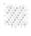
- FIG. 1 is a schematic plan view of a capacitor according to a first embodiment of the present invention.
- FIG. 2 is a schematic cross-sectional view taken along the line II-II of FIG.
- FIG. 3 is a schematic cross-sectional view taken along the line III-III of FIG.
- FIG. 4 is a schematic cross-sectional view taken along the line IV-IV of FIG. 5A is a cross-sectional view showing a part of the manufacturing process of the semiconductor device shown in FIGS. 1 and 2, and is a cross-sectional view corresponding to the cut surface of FIG.
- FIG. 5B is a cross-sectional view showing the next step of FIG. 5A.
- FIG. 5C is a cross-sectional view showing the next step of FIG. 5B.
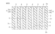
- FIG. 5D is a cross-sectional view showing the next step of FIG. 5C.
- FIG. 5E is a cross-sectional view showing the next step of FIG. 5D.
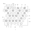
- FIG. 6 is a schematic plan view showing a modified example of the cross-sectional shape of the first internal electrode forming through hole and the second internal electrode forming through hole.
- FIG. 7 is a schematic plan view showing another modification of the cross-sectional shape of the first internal electrode forming through hole and the second internal electrode forming through hole.
- FIG. 8 is a schematic plan view showing a modified example of the arrangement of the first internal electrode forming through hole and the second internal electrode forming through hole.
- FIG. 9 is a schematic plan view showing an arrangement of a first internal electrode forming through hole and a second internal electrode forming through hole and a modified example of the cross-sectional shape.
- FIG. 10 is a schematic plan view showing the arrangement of the first internal electrode forming through hole and the second internal electrode forming through hole and still another modification of the cross-sectional shape.
- FIG. 11 is a schematic plan view showing the arrangement of the first internal electrode forming through hole and the second internal electrode forming through hole and still another modification of the cross-sectional shape.
- FIG. 12 is a schematic plan view showing the arrangement of the first internal electrode forming through hole and the second internal electrode forming through hole and still another modification of the cross-sectional shape.
- FIG. 13 is a schematic plan view showing the arrangement of the first internal electrode forming through hole and the second internal electrode forming through hole and still another modification of the cross-sectional shape.
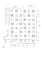
- FIG. 14 is a schematic plan view of the capacitor according to the second embodiment of the present invention.
- FIG. 15 is a schematic cross-sectional view taken along the line XV-XV of FIG.
- FIG. 16 is a schematic configuration diagram of a semiconductor package in which the capacitors shown in FIGS. 1 and 2 are packaged.
- FIG. 1 is a schematic plan view of the capacitor according to the first embodiment of the present invention.
- FIG. 2 is a schematic cross-sectional view taken along the line II-II of FIG.
- FIG. 3 is a schematic cross-sectional view taken along the line III-III of FIG.
- FIG. 4 is a schematic cross-sectional view taken along the line IV-IV of FIG.
- the first insulating film 7 and the first external electrode 8 of FIG. 2 are omitted.
- the first internal electrode 5 is indicated by dot-shaped hatching, and the second internal electrode 6 is indicated by cross-hatching. ing.
- the vertical direction in FIG. 1 will be referred to as the vertical direction
- the horizontal direction in FIG. 1 will be referred to as the horizontal direction.
- the capacitor 1 has a rectangular parallelepiped shape.
- the capacitor 1 includes a substrate 2.
- the substrate 2 has a rectangular parallelepiped shape and includes a pair of main surfaces 2a and 2b and four side surfaces 2c. Of the pair of main surfaces 2a and 2b, the main surface 2a on the upper surface side in FIG. 2 is referred to as "first main surface 2a", and the main surface 2b on the opposite side to the first main surface 2a is referred to as "second main surface 2b". ..
- the substrate 2 In a plan view seen from the normal direction orthogonal to the first main surface 2a, the substrate 2 has a square shape, and the length of one side thereof is, for example, about 5 mm.
- the plan view shape of the substrate 2 may be a shape other than a square shape such as a rectangular shape or a circular shape.
- the thickness of the substrate 2 is, for example, 100 ⁇ m or more, and in this embodiment, it is, for example, about 400 ⁇ m.
- the substrate 2 is made of silicon oxide (SiO 2 ) obtained by thermally oxidizing a silicon substrate.
- the substrate 2 may be a silicon substrate.
- the substrate 2 is formed with a plurality of first internal electrode forming through holes 3 penetrating the substrate 2 in the thickness direction and a plurality of second internal electrode forming through holes 4 penetrating the substrate 2 in the thickness direction.
- a plurality of internal electrode forming through holes 3 and 4 including a plurality of first internal electrode forming through holes 3 and a plurality of second internal electrode forming through holes 4 are arranged in a grid pattern in a plan view. ..
- the plurality of internal electrode forming through holes 3 and 4 are arranged in a matrix in a plan view.
- the plurality of internal electrode forming through holes 3 and 4 are arranged side by side at equal intervals in the vertical direction and the horizontal direction in a plan view.
- each of the internal electrode forming through holes 3 and 4 is square in this embodiment, and the length of one side thereof is, for example, about 0.3 ⁇ m or more and 10 ⁇ m or less. In this embodiment, the length of one side is, for example, about 5 ⁇ m.
- the depths of the through holes 3 and 4 for forming the internal electrodes are the same as the thickness of the substrate 2.
- the first internal electrode forming through hole 3 and the second internal electrode forming through hole 4 are arranged alternately in the vertical direction and the horizontal direction, respectively.
- a first internal electrode 5 made of a conductor is embedded in each through hole 3 for forming the first internal electrode.
- a second internal electrode 6 made of a conductor is embedded in each of the through holes 4 for forming the second internal electrode.
- the distance between the plurality of internal electrodes 5 and 6 including the first internal electrode 5 and the second internal electrode 6 is about 0.3 ⁇ m or more and 10 ⁇ m or less.
- the first internal electrode 5 is an inside embedded in the first internal electrode forming through hole 3 while being surrounded by the seed layer 5A formed on the inner surface of the first internal electrode forming through hole 3 and the seed layer 5A. It is composed of an electrode layer 5B.
- the seed layer 5A and the internal electrode layer 5B are made of copper (Cu).
- the seed layer 5A and the internal electrode layer 5B may be made of a metal such as Al, Pt, Au, Ag, or Ni or polysilicon.
- the second internal electrode 6 is an internal portion embedded in the second internal electrode forming through hole 4 while being surrounded by the seed layer 6A formed on the inner surface of the second internal electrode forming through hole 4 and the seed layer 6A. It is composed of an electrode layer 6B.
- the seed layer 6A and the internal electrode layer 6B are made of copper (Cu).
- the seed layer 6A and the internal electrode layer 6B may be made of a metal such as Al, Pt, Au, Ag, Ni, or polysilicon.
- a first insulating film 7 is formed on the first main surface 2a of the substrate 2 so as to cover the first main surface 2a and the second internal electrode 6.
- the first insulating film 7 is formed with a first contact hole 7a that exposes an end portion of the first internal electrode 5 on the side of the first main surface.
- the first insulating film 7 is made of, for example, a SiO 2 film.
- the first insulating film 7 may be composed of a SiN film, a SiON film, or the like.
- the plan-view shape of the first contact hole 7a is a square shape having a size substantially equal to the size of the cross section of the first internal electrode 5.
- the plan-view shape of the first contact hole 7a may be a shape other than a square shape, such as a rectangular shape or a circular shape.
- the first external electrode 8 is placed on the first main surface 2a of the substrate 2 so as to cover at least a part of the exposed surface of the first insulating film 7 and all the ends of the first internal electrode 5 on the first main surface side. Is formed.
- the first external electrode 8 enters the first contact hole 7a of the first insulating film 7, and is connected to the first main surface side end portion of the first internal electrode 5 in the first contact hole 7a. As a result, the first external electrode 8 is electrically connected to the first internal electrode 5.
- the exposed surfaces other than the outer surface of the first insulating film 7 are covered with the first external electrode 8.
- the first external electrode 8 is a seed layer 8A formed so as to cover the exposed surface (excluding the outer surface) of the first insulating film 7 and the exposed surface of all the first main surface side ends of the first internal electrodes 5. And an external electrode layer 8B laminated on the seed layer 8A.
- the seed layer 8A and the external electrode layer 8B are made of copper (Cu).
- the seed layer 8A may be composed of Al, Pt, Au, Ag, Ni, etc. in addition to Cu.
- the external electrode layer 8B may be composed of Al, Pt, Au, Ag, Ni, etc. in addition to Cu.
- a second insulating film 9 is formed on the second main surface 2b of the substrate 2 so as to cover the second main surface 2B and the first internal electrode 5.
- the second insulating film 9 is formed with a second contact hole 9a that exposes the end on the side of the second main surface of the second internal electrode 6.
- the second insulating film 9 is made of, for example, a SiO 2 film.
- the second insulating film 9 may be composed of a SiN film, a SiON film, or the like.
- the plan-view shape of the second contact hole 9a is a square shape having a size substantially equal to the size of the cross section of the second internal electrode 6.
- the plan-view shape of the second contact hole 9a may be a shape other than a square shape, such as a rectangular shape or a circular shape.
- the second external electrode 10 is placed on the second main surface 2b of the substrate 2 so as to cover at least a part of the exposed surface of the second insulating film 9 and the second main surface side end portion of all the second internal electrodes 6. Is formed.
- the second external electrode 10 enters the second contact hole 9a of the second insulating film 9 and is connected to the second main surface side end portion of the second internal electrode 6 in the second contact hole 9a.
- the second external electrode 10 is electrically connected to the second internal electrode 6.
- the exposed surfaces other than the outer surface of the second insulating film 9 are covered with the second external electrode 10.
- the second external electrode 10 is a seed formed so as to cover the exposed surface (excluding the outer surface) of the second insulating film 9 and the exposed surface of all the second main surface side ends of all the second internal electrodes 6. It is composed of a layer 10A and an external electrode layer 10B laminated on the seed layer 10A.
- the seed layer 10A and the external electrode layer 10B are made of copper (Cu).
- the seed layer 10A may be composed of Al, Pt, Au, Ag, Ni, etc. in addition to Cu.
- the external electrode layer 10B may be composed of Al, Pt, Au, Ag, Ni, etc. in addition to Cu.
- first internal electrode 5 and the second internal electrode 6 adjacent to each other in the vertical direction have facing surfaces facing each other in the vertical direction.
- the wall of the substrate 2 sandwiched between the facing surfaces of the first internal electrode 5 and the second internal electrode 6 adjacent to each other in the vertical direction constitutes a capacitive film (dielectric film).
- a set of vertically adjacent first internal electrodes 5, second internal electrodes 6, and a capacitive film between them constitutes one capacitor element.
- first internal electrode 5 and the second internal electrode 6 adjacent to each other in the lateral direction have facing surfaces facing each other in the lateral direction.
- the wall of the substrate 2 sandwiched between the facing surfaces of the first internal electrode 5 and the second internal electrode 6 adjacent to each other in the lateral direction constitutes a capacitive film (dielectric film).
- a set of first internal electrodes 5 and second internal electrodes 6 adjacent to each other in the lateral direction and a capacitive film between them constitute one capacitor element.
- a first internal electrode forming through hole 3 and a second internal electrode forming through hole 4 are formed in the substrate 2, and a conductor is embedded in these internal electrode forming through holes 3 and 4, so that the first internal portion is formed. Since the electrode 5 and the second internal electrode 6 can be formed, the first internal electrode 5 and the second internal electrode 6 can be easily manufactured. This makes it possible to provide a capacitor that is easy to manufacture.
- 5A to 5E are cross-sectional views for explaining an example of a capacitor manufacturing process, and show a cut surface corresponding to FIG. 2.
- the original substrate 40 which is the source of the substrate 2 is prepared.
- the original substrate 40 has a first main surface 40a, a second main surface 40b opposite to the first main surface 40a, and four side surfaces 40c connecting the first main surface 40a and the second main surface 40b. doing.
- the original substrate 40 is a silicon substrate.
- a first internal electrode forming through hole 3 and a second internal electrode forming through hole 4 are formed by an electrochemical etching method. These internal electrode forming through holes 3 and 4 may be formed by laser processing.
- the entire original substrate 40 is formed into a thermal oxide film by the thermal oxidation method.
- the original substrate 40 becomes the substrate 2 made of SiO 2.
- the first main surface 40a of the original substrate 40 is the first main surface 2a of the substrate 2
- the second main surface 40b of the original substrate 40 is the second main surface 2b of the substrate 2
- the side surface 40c of the original substrate 40 is the substrate. It is the side surface 2c of 2.
- the seed layer 5A is formed on the inner surface of the first internal electrode forming through hole 3, and at the same time, the seed layer 6A is formed on the inner surface of the second internal electrode forming through hole 4. ..
- the seed layers 5A and 6A are, for example, Cu seed layers.
- the seed layers 5A and 6A are formed by, for example, an atomic layer deposition method (ALD: Atomic Layer Deposition).
- the internal electrode layer 5B is formed on the seed layer 5A in the first internal electrode forming through hole 3 by, for example, the plating method, and at the same time, the second internal electrode forming through hole 4 is formed.
- an internal electrode layer 6B is formed on the seed layer 6A.
- the internal electrode layer 5B and the internal electrode layer 6B are made of, for example, Cu.
- the first internal electrode 5 composed of the seed layer 5A and the internal electrode layer 5B is embedded in the through hole 3 for forming the first internal electrode.
- the second internal electrode 6 composed of the seed layer 6A and the internal electrode layer 6B is embedded in the through hole 4 for forming the second internal electrode.
- the first insulating film 7 is formed so as to cover the end on the side of the first main surface of 6.
- the first insulating film 7 may be formed by a chemical vapor deposition method (CVD).
- the first insulating film 7 is made of, for example, a SiO 2 film.
- a first contact hole 7a that exposes the first main surface side end portion of the first internal electrode 5 is formed in the first insulating film 7.
- a second insulating film 9 is formed so as to cover the end portion.
- the second insulating film 9 may be formed by a CVD method.
- the second insulating film 9 is made of, for example, a SiO 2 film.
- a second contact hole 9a that exposes the second main surface side end portion of the second internal electrode 6 is formed in the second insulating film 9.
- first external electrode 8 is formed on the first main surface 2a of the substrate 2
- second external electrode 10 is formed on the second main surface 2b of the substrate 2, so that FIGS. 1 and 2 show.
- the indicated capacitor 1 is obtained.
- the first external electrode 8 is formed, for example, as follows. First, for example, the seed layer 8A is formed by a sputtering method so as to cover the exposed surface (excluding the outer surface) of the first insulating film 7 and the exposed surface of the first main surface side end portion of all the first internal electrodes 5. Will be done. Then, for example, the external electrode layer 8B is formed on the seed layer 8A by a plating method. As a result, the first external electrode 8 composed of the seed layer 8A and the external electrode layer 8B and electrically connected to all the first internal electrodes 5 is formed on the first main surface 2a.
- the second external electrode 10 is formed, for example, as follows. First, for example, the seed layer 10A is formed by a sputtering method so as to cover the exposed surface (excluding the outer surface) of the second insulating film 9 and the exposed surface of the second main surface side end portion of all the second internal electrodes 6. Will be done. Then, for example, the external electrode layer 10B is formed on the seed layer 10A by a plating method. As a result, the second external electrode 10 composed of the seed layer 10A and the external electrode layer 10B and electrically connected to all the second internal electrodes 6 is formed on the second main surface 2b.
- FIG. 6 to 13 are plan views showing a modified example in which one or both of the cross-sectional shapes of the first internal electrode forming through hole 3 and the second internal electrode forming through hole 4 and their arrangement are different, respectively. Yes, it is a plan view corresponding to FIG. 6 to 13, each part corresponding to FIG. 1 is designated by the same reference numerals as those in FIG.
- the cross-sectional shape of the first internal electrode forming through hole 3 and the second internal electrode forming through hole 4 may be circular.
- the cross-sectional shape of the first internal electrode 5 embedded in the first internal electrode forming through hole 3 and the second internal electrode 6 embedded in the second internal electrode forming through hole 4 is also circular.
- the cross-sectional shape of the first internal electrode forming through hole 3 and the second internal electrode forming through hole 4 may be a regular hexagonal shape.
- the cross-sectional shape of the first internal electrode 5 embedded in the first internal electrode forming through hole 3 and the second internal electrode 6 embedded in the second internal electrode forming through hole 4 is also a regular hexagonal shape. ..
- a plurality of internal electrode forming through holes 3 and 4 including a plurality of first internal electrode forming through holes 3 and a plurality of second internal electrode forming through holes 4 may be formed. They may be arranged in a staggered pattern in a plan view.
- each of the internal electrode forming through holes 3 and 4 is square as in FIG. 1.
- the first internal electrode forming through hole 3 and the second internal electrode forming through hole 4 are arranged alternately side by side only in the lateral direction.
- the cross-sectional shape of each of the internal electrode forming through holes 3 and 4 is circular.
- each of the internal electrode forming through holes 3 and 4 is a regular hexagonal shape.
- the horizontal arrangement of the internal electrode forming through holes 3 and 4 is referred to as a row
- the vertical arrangement of the internal electrode forming through holes 3 and 4 is a column
- each row is the lower side of the drawing. From to the upper side, the first line, the second line, the third line, ..., The Nth line.
- the left end of the even-numbered line is shifted to the left with respect to the left end of the odd-numbered line.
- the first internal electrode forming through hole 3 and the second internal electrode forming through hole 4 are alternately arranged in the lateral direction.
- the first internal electrode forming through hole 3 is arranged at the left end.
- the left end in the odd-numbered rows is vertically arranged with the first internal electrode forming through hole 3 and the second internal electrode forming through hole 4, and the left end in the even-numbered row is.
- the first internal electrode forming through hole 3 and the second internal electrode forming through hole 4 are alternately arranged in the vertical direction.
- the third through hole for forming the internal electrode in the sixth row from the left is the through hole 4 for forming the second internal electrode.
- the first internal electrode is formed in a substantially annular shape or a substantially arc shape centered on the basic through hole 4.
- the through holes 3 and the through holes 4 for forming the second internal electrode are alternately arranged.
- the cross-sectional shapes of the through holes 3 and 4 for forming internal electrodes are circular, but the arrangement of all of them in a plan view is the same matrix as in FIG. However, the arrangement of the first internal electrode forming through hole 3 and the second internal electrode forming through hole 4 is different from that of FIG.
- the horizontal arrangement of the internal electrode forming through holes 3 and 4 is referred to as a row
- the vertical arrangement of the internal electrode forming through holes 3 and 4 is a row
- each row is arranged from left to right.
- the first column, the second column, the third column, ..., The sixth column, and each row is referred to as the first row, the second row, the third row, ..., The sixth matrix from the bottom to the top.
- the first row and the fourth row are all composed of through holes 3 for forming the first internal electrode.
- the third row and the sixth row are all composed of the through holes 4 for forming the second internal electrode.
- the third and fifth rows are composed of the first internal electrode forming through hole 3, and the first, second, fourth and sixth rows are composed of the second internal electrode forming through hole 4.
- the second and fourth rows are composed of the first internal electrode forming through hole 3
- the first, third, fifth and sixth rows are composed of the second internal electrode forming through hole 4. Has been done.
- FIG. 14 is a schematic plan view of the capacitor according to the second embodiment of the present invention.
- FIG. 15 is a schematic cross-sectional view taken along the line XV-XV of FIG.
- the first insulating film 7 and the main first external electrode 81 of FIG. 15 are omitted.
- the first internal electrode 5 is indicated by dot-shaped hatching, and the second internal electrode 6 is indicated by cross-hatching. ing.
- FIG. 14 the parts corresponding to the respective parts of FIG. 1 are designated by the same reference numerals as those in FIG.
- the parts corresponding to the parts of FIG. 2 are designated by the same reference numerals as those in FIG.
- the vertical direction of FIG. 14 will be referred to as the vertical direction
- the horizontal direction of FIG. 14 will be referred to as the horizontal direction.
- Capacitor 1A has a rectangular parallelepiped shape. Capacitor 1A includes a substrate 2.
- the substrate 2 has a rectangular parallelepiped shape and includes a pair of main surfaces 2a and 2b and four side surfaces 2c. Of the pair of main surfaces 2a and 2b, the main surface 2a on the upper surface side in FIG. 15 is referred to as "first main surface 2a", and the main surface 2b opposite to the first main surface 2a is referred to as "second main surface 2b". .. In a plan view viewed from the normal direction orthogonal to the first main surface 2a, the substrate 2 has a rectangular shape, the length of the long side thereof is, for example, about 10 mm, and the length of the short side is, for example, about 5 mm. be.
- the thickness of the substrate 2 is, for example, 100 ⁇ m or more, and in this embodiment, it is, for example, about 400 ⁇ m.
- the substrate 2 is made of silicon oxide (SiO 2 ) obtained by thermally oxidizing a silicon substrate.
- the substrate 2 may be a silicon substrate.
- the substrate 2 is formed with a plurality of first internal electrode forming through holes 3, a plurality of second internal electrode forming through holes 4, and a plurality of external electrode connecting through holes 21 that penetrate the substrate 2 in the thickness direction.
- a plurality of internal electrode forming through holes 3 and 4 including a plurality of first internal electrode forming through holes 3 and a plurality of second internal electrode forming through holes 4 are arranged in a matrix in a plan view. ..
- the plurality of internal electrode forming through holes 3 and 4 are arranged side by side at equal intervals in the vertical direction and the horizontal direction in a plan view.
- the plurality of external electrode connecting through holes 21 are arranged vertically on one side (in this example, the left side of FIG. 14) of the plurality of internal electrode forming through holes 3 and 4 arranged in a matrix in a plan view. Have been placed.
- a plurality of through holes 3 and 4 including a plurality of first internal electrode forming through holes 3, a plurality of second internal electrode forming through holes 4, and a plurality of external electrode connecting through holes 21. , 21 are also arranged in a matrix.
- the plurality of through holes 3, 4, 21 are arranged side by side at equal intervals in the vertical direction and the horizontal direction in a plan view.
- each of the through holes 3, 4, 21 is square in this embodiment, and the length of one side thereof is, for example, about 0.3 ⁇ m or more and 10 ⁇ m or less. In this embodiment, the length of one side is, for example, about 5 ⁇ m.
- the first internal electrode forming through hole 3 and the second internal electrode forming through hole 4 are arranged alternately in the vertical direction and the horizontal direction, respectively.
- the region on the right side of the vertical virtual straight line L1 passing through the left ends of the through holes 3 and 4 for forming internal electrodes in a plan view is referred to as the first region S1. Further, on the second main surface 2b of the substrate 2, the region on the left side of the vertical virtual straight line L2 passing through the right end of the external electrode connection through hole 21 in a plan view is referred to as the second region S2.
- a first internal electrode 5 made of a conductor is embedded in each through hole 3 for forming the first internal electrode.
- a second internal electrode 6 made of a conductor is embedded in each of the through holes 4 for forming the second internal electrode.
- An external electrode connecting member 22 made of a conductor is embedded in the external electrode connecting through hole 21.
- the distance between the plurality of internal electrodes 5 and 6 including the first internal electrode 5 and the second internal electrode 6 is about 0.3 ⁇ m or more and 10 ⁇ m or less.
- the first internal electrode 5 is an inside embedded in the first internal electrode forming through hole 3 while being surrounded by the seed layer 5A formed on the inner surface of the first internal electrode forming through hole 3 and the seed layer 5A. It is composed of an electrode layer 5B.
- the seed layer 5A and the internal electrode layer 5B are made of copper (Cu).
- the seed layer 5A and the internal electrode layer 5B may be made of a metal such as Al, Pt, Au, Ag, or Ni or polysilicon.
- the second internal electrode 6 is an internal portion embedded in the second internal electrode forming through hole 4 while being surrounded by the seed layer 6A formed on the inner surface of the second internal electrode forming through hole 4 and the seed layer 6A. It is composed of an electrode layer 6B.
- the seed layer 6A and the internal electrode layer 6B are made of copper (Cu).
- the seed layer 6A and the internal electrode layer 6B may be made of a metal such as Al, Pt, Au, Ag, Ni, or polysilicon.
- the external electrode connecting member 22 is surrounded by a seed layer 22A formed on the inner surface of the external electrode connecting through hole 21 and an external electrode connecting layer 22B embedded in the external electrode connecting through hole 21 in a state of being surrounded by the seed layer 22A. It consists of.
- the seed layer 22A and the external electrode connecting layer 22B are made of copper (Cu).
- the seed layer 22A and the external electrode connecting layer 22B may be made of a metal such as Al, Pt, Au, Ag, or Ni or polysilicon.
- a first insulating film 7 is formed on the first main surface 2a of the substrate 2 so as to cover the first main surface 2a and the second internal electrode 6.
- the first insulating film 7 has a first contact hole 7a that exposes the first main surface side end portion of the first internal electrode 5, and a third contact hole that exposes the first main surface side end portion of the external electrode connecting member 22. 7b is formed.
- the first insulating film 7 is made of, for example, a SiO 2 film.
- the first insulating film 7 may be composed of a SiN film, a SiON film, or the like.
- the plan-view shapes of the first contact hole 7a and the third contact hole 7b are square shapes having a size substantially equal to the size of the cross section of the first internal electrode 5 and the external electrode connecting member 22, respectively. ..
- the main first external electrode covers at least a part of the exposed surface of the first insulating film 7 and the first main surface side end portion of all the first internal electrodes 5. 81 is formed.
- the main first external electrode 81 enters the first contact hole 7a of the first insulating film 7, and is connected to the first main surface side end portion of the first internal electrode 5 in the first contact hole 7a.
- the main first external electrode 81 is electrically connected to the first internal electrode 5.
- the exposed surfaces other than the outer surface of the first insulating film 7 are covered with the main first external electrode 81.
- the main first external electrode 81 enters the third contact hole 7b and is connected to the first main surface side end portion of the external electrode connecting member 22 in the third contact hole 7b. As a result, the main first external electrode 81 is electrically connected to the external electrode connecting member 22.
- the main first external electrode 81 is an exposed surface (excluding the outer surface) of the first insulating film 7, an exposed surface at the end of the first main surface side of all the first internal electrodes 5, and all the external electrode connecting members 22. It is composed of a seed layer 81A formed so as to cover the end on the side of the first main surface, and an external electrode layer 81B laminated on the seed layer 81A.
- the seed layer 81A and the external electrode layer 81B are made of copper (Cu).
- the seed layer 81A may be composed of Al, Pt, Au, Ag, Ni, etc. in addition to Cu.
- the external electrode layer 81B may be composed of Al, Pt, Au, Ag, Ni, etc. in addition to Cu.
- a second insulating film 9 is formed on the second main surface 2b of the substrate 2 so as to cover the second main surface 2B and the first internal electrode 5.
- the second insulating film 9 has a second contact hole 9a that exposes the second main surface side end portion of the second internal electrode 6, and a fourth contact hole that exposes the second main surface side end portion of the external electrode connecting member 22. 9b is formed.
- the second insulating film 9 is made of, for example, a SiO 2 film.
- the second insulating film 9 may be composed of a SiN film, a SiON film, or the like.
- the plan-view shapes of the second contact hole 9a and the fourth contact hole 9b are square shapes having a size substantially equal to the size of the cross section of the second internal electrode 6 and the external electrode connecting member 22, respectively. ..
- the second external electrode 10 is formed.
- the second external electrode 10 enters the second contact hole 9a of the second insulating film 9 and is connected to the second main surface side end portion of the second internal electrode 6 in the second contact hole 9a.
- the second external electrode 10 is electrically connected to the second internal electrode 6.
- the exposed surface of the second insulating film 9 other than the outer surface of the second insulating film 9 is covered with the second external electrode 10.
- the second external electrode 10 covers the exposed surface (excluding the outer surface) of the second insulating film 9 and the exposed surface of the second main surface side end portion of all the second internal electrodes 6 in the first region S1. It is composed of the formed seed layer 10A and the external electrode layer 10B laminated on the seed layer 10A.
- the seed layer 10A and the external electrode layer 10B are made of copper (Cu).
- the seed layer 10A may be composed of Al, Pt, Au, Ag, Ni, etc. in addition to Cu.
- the external electrode layer 10B may be composed of Al, Pt, Au, Ag, Ni, etc. in addition to Cu.
- the sub-first external electrode 82 is formed.
- the sub-first external electrode 82 enters the fourth contact hole 9b of the second insulating film 9, and is connected to the second main surface side end portion of the external electrode connecting member 22 in the fourth contact hole 9b.
- the sub-first external electrode 82 is electrically connected to the external electrode connecting member 22.
- the exposed surfaces other than the outer surface of the second insulating film 9 are covered with the sub-first external electrode 82.
- the sub-first external electrode 82 is electrically connected to the main first external electrode 81 via the external electrode connecting member 22. That is, in this embodiment, the first external electrode 80 is composed of the main first external electrode 81 and the sub first external electrode 82. In other words, the first external electrode 80 includes a main first external electrode 81 formed on the first main surface 2a side of the substrate 2 and a sub first external electrode 82 formed on the second main surface 2b side of the substrate 2. And is included.
- the sub-first external electrode 82 covers the exposed surface (excluding the outer surface) of the second insulating film 9 and the exposed surface of the second main surface side end portion of all the external electrode connecting members 22 in the second region S2. It is composed of a seed layer 82A formed in the above and an external electrode layer 82B laminated on the seed layer 82A.
- the seed layer 8A and the external electrode layer 82B are made of copper (Cu).
- the seed layer 82A may be composed of Al, Pt, Au, Ag, Ni, etc. in addition to Cu.
- the external electrode layer 82B may be composed of Al, Pt, Au, Ag, Ni, etc. in addition to Cu.
- the first external electrode 80 includes a main first external electrode 81 formed on the first main surface 2a side of the substrate 2 and a sub first external electrode formed on the second main surface 2b side of the substrate 2. Includes an electrode 82. Therefore, the wiring for connecting to the first external electrode 80 can be connected to the main first external electrode 81 on the first main surface 2a side of the substrate 2, and the second main surface 2b of the substrate 2 can be connected. It is possible to connect to the sub first external electrode 82 on the side. Further, the second external electrode 10 and the sub-first external electrode 82 can be directly joined to the wiring pattern on the printed circuit board.
- FIG. 16 is a schematic configuration diagram of a semiconductor package in which the capacitors 1 shown in FIGS. 1 and 2 are packaged.
- the semiconductor package 101 includes a flat rectangular parallelepiped resin package 102, and a first terminal 103 and a second terminal 104 sealed in the resin package 102.
- the two terminals 103 and 104 are made of a metal plate formed in a predetermined shape.
- the second terminal 104 is formed in a shape including a square island 105 and an elongated rectangular terminal portion 106 extending linearly from one side of the island 105.
- the first terminal 103 is formed in substantially the same shape as the terminal portion 106 of the second terminal 104, and is arranged in a state parallel to the terminal portion 106 of the second terminal 104.
- the capacitor 1 is die-bonded on the second terminal 104 (the central portion of the island 105).
- the island 105 is joined to the second external electrode 10 of the capacitor 1 from below.
- the first terminal 103 is connected to the first external electrode 8 of the capacitor 1 by using a bonding wire 107.
- the cross-sectional shape of the first internal electrode forming through hole 3 and the second internal electrode forming through hole 4 is not limited to the above-mentioned shape, and may be any shape.
- the cross-sectional shape of the first internal electrode forming through hole 3 and the second internal electrode forming through hole 4 may be, for example, a rectangular shape long in one direction. In this case, the first internal electrode 5 and the second internal electrode 6 have a flat plate shape.
- the plurality of internal electrode forming through holes 3 and 4 including the plurality of first internal electrode forming through holes 3 and the plurality of second internal electrode forming through holes 4 are in a grid pattern. They are arranged in a matrix or staggered pattern, but they do not have to be arranged in a grid pattern. For example, they may be arranged in a row.
Landscapes
- Engineering & Computer Science (AREA)
- Power Engineering (AREA)
- Microelectronics & Electronic Packaging (AREA)
- Manufacturing & Machinery (AREA)
- Semiconductor Integrated Circuits (AREA)
- Fixed Capacitors And Capacitor Manufacturing Machines (AREA)
- Ceramic Capacitors (AREA)
Abstract
キャパシタは、一方側の第1主面および他方側の第2主面を有する基板2と、基板を厚さ方向に貫通する複数の第1内部電極形成用貫通孔3と、基板を厚さ方向に貫通する複数の第2内部電極形成用貫通孔4と、第1内部電極形成用貫通孔内に埋め込まれた導電体からなる第1内部電極5と、第2内部電極形成用貫通孔内に埋め込まれた導電体からなる第2内部電極6とを含む。複数の第1内部電極形成用貫通孔3と複数の第2内部電極形成用貫通孔4とを含む複数の内部電極形成用貫通孔3,4は、第1主面に直交する法線方向から見た平面視において、格子状に配置されている。
Description
この発明は、キャパシタおよびキャパシタの製造方法に関する。
特許文献1の図1および図2には、基体の一方の面(上面)に形成された第1開口部に埋め込まれた第1埋込電極と、基体の他方の面(下面)に形成された第2開口部に埋め込まれた第2埋込電極とを有する容量素子が開示されている。基体は、シリコン基板と、シリコン基板上に積層された酸化シリコン層(BOX層)とからなる。第1開口部は基体を貫通していない上方開口の凹部である。また、第2開口部は基体を貫通していない下方開口の凹部である。
特許文献1の図2に示すように、第1埋込電極と第2埋込電極とは、平面視において両者が互いに入り込んだ櫛歯状に配置されている。なお、特許文献1には、特許文献1の図3に示すように、第1埋込電極と第2埋込電極とは、平面視において、中央部に配置された円状の第1埋込電極と、その円状の第1埋込電極と同心円状に交互に配置された環状の第2埋込電極および環状の第1電極とから構成されてもよいことが開示されている。
この発明の目的は、新規な構成のキャパシタを提供することである。
また、この発明の目的は、新規なキャパシタの製造方法を提供することである。
この発明の一実施形態は、一方側の第1主面および他方側の第2主面を有する基板と、前記基板を厚さ方向に貫通する複数の第1内部電極形成用貫通孔と、前記基板を厚さ方向に貫通する複数の第2内部電極形成用貫通孔と、前記第1内部電極形成用貫通孔内に埋め込まれた導電体からなる第1内部電極と、前記第2内部電極形成用貫通孔内に埋め込まれた導電体からなる第2内部電極とを含み、前記複数の第1内部電極形成用貫通孔と前記複数の第2内部電極形成用貫通孔とを含む複数の内部電極形成用貫通孔は、前記第1主面に直交する法線方向から見た平面視において、格子状に配置されている、キャパシタを提供する。この実施形態によれば、新規な構成のキャパシタが得られる。
この発明の一実施形態では、前記複数の内部電極形成用貫通孔は、前記平面視において、行列状に配置されている。
この発明の一実施形態では、前記複数の内部電極形成用貫通孔は、前記平面視において、千鳥状に配置されている。
この発明の一実施形態では、前記第1主面上に配置され、前記複数の第1内部電極が電気的に接続された第1外部電極と、前記第2主面上に配置され、前記複数の第2内部電極が電気的に接続された第2外部電極とを含む。
この発明の一実施形態では、前記第2内部電極の前記第1主面側端部を覆うように前記第1主面上に形成され、前記第1内部電極の前記第1主面側端部を露出させる第1コンタクト孔を有する第1絶縁膜と、前記第1内部電極の前記第2主面側端部を覆うように前記第2主面上に形成され、前記第2内部電極の前記第2主面側端部を露出させる第2コンタクト孔を有する第2絶縁膜とをさらに含み、前記第1外部電極は、前記第1絶縁膜の露出面の少なくとも一部および前記複数の第1内部電極の前記第1主面側端部を覆うように、前記第1主面上に形成されており、前記第2外部電極は、前記第2絶縁膜の露出面の少なくとも一部および前記複数の第2内部電極の前記第2主面側端部を覆うように、前記第2主面上に形成されており、前記第1外部電極は、前記第1コンタクト孔内に入り込み、前記第1コンタクト孔内で前記第1内部電極に接続されており、前記第2外部電極は、前記第2コンタクト孔内に入り込み、前記第2コンタクト孔内で前記第2内部電極に接続されている。
この発明の一実施形態では、前記第1内部電極形成用貫通孔および前記第2内部電極形成用貫通孔のアスペクト比が50以上である。
この発明の一実施形態では、前記第1内部電極形成用貫通孔および前記第2内部電極形成用貫通孔の深さが100μm以上である。
この発明の一実施形態では、前記第1内部電極形成用貫通孔および前記第2内部電極形成用貫通孔の横断面の最大幅または最大径が、0.3μm以上10μm以下である。
この発明の一実施形態では、前記第1内部電極および第2内部電極を含む複数の内部電極の電極間距離が、0.3μm以上10μm以下である。
この発明の一実施形態では、前記導電体がCu、Al、Pt、Au、Ag、Niおよびポリシリコンから任意に選択された1からなる。
この発明の一実施形態は、一方側の第1主面および他方側の第2主面を有する基板と、前記基板を厚さ方向に貫通する複数の第1内部電極形成用貫通孔と、前記基板を厚さ方向に貫通する複数の第2内部電極形成用貫通孔と、前記第1内部電極形成用貫通孔内に埋め込まれた導電体からなる第1内部電極と、前記第2内部電極形成用貫通孔内に埋め込まれた導電体からなる第2内部電極と、前記第2内部電極の前記第1主面側端部を覆うように前記第1主面上に形成され、前記第1内部電極の前記第1主面側端部を露出させる第1コンタクト孔を有する第1絶縁膜と、前記第1内部電極の前記第2主面側端部を覆うように前記第2主面上に形成され、前記第2内部電極の前記第2主面側端部を露出させる第2コンタクト孔を有する第2絶縁膜と、前記第1主面上に、前記第1絶縁膜の露出面の少なくとも一部および前記複数の第1内部電極の前記第1主面側端部を覆うように形成され、かつ前記複数の第1内部電極が電気的に接続された第1外部電極と、前記第2主面上に、前記第2絶縁膜の露出面の少なくとも一部および前記複数の第2内部電極の前記第2主面側端部を覆うように形成され、かつ前記複数の第2内部電極が電気的に接続された第2外部電極とを含む、キャパシタを提供する。この実施形態によれば、新規な構成のキャパシタが得られる。
この発明の一実施形態では、前記第1外部電極は、前記第1コンタクト孔内に入り込み、前記第1コンタクト孔内で前記第1内部電極に接続されており、前記第2外部電極は、前記第2コンタクト孔内に入り込み、前記第2コンタクト孔内で前記第2内部電極に接続されている。
この発明の一実施形態は、一方側の第1主面および他方側の第2主面を有する基板に、前記基板を厚さ方向に貫通する複数の第1内部電極形成用貫通孔と、前記基板を厚さ方向に貫通する複数の第2内部電極形成用貫通孔とを形成する第1工程と、前記第1電極形成用貫通孔内および前記第2内部電極形成用貫通孔内に導電体を埋め込むことにより、前記第1内部電極形成用貫通孔内に第1内部電極を形成するとともに前記第2内部電極形成用貫通孔内に第2内部電極を形成する第2工程とを含む、キャパシタの製造方法を提供する。この実施形態によれば、新規なキャパシタの製造方法を提供できる。
この発明の一実施形態では、前記第1内部電極および前記第2内部電極の前記第1主面側端部を覆うように、前記第1主面上に第1絶縁層を形成する第3工程と、前記第1内部電極の前記第1主面側端部を露出させる第1コンタクト孔を、前記第1絶縁層に形成する第4工程と、前記第1内部電極および前記第2内部電極の前記第2主面側端部を覆うように、前記第2主面上に第2絶縁層を形成する第5工程と、前記第2内部電極の前記第2主面側端部を露出させる第2コンタクト孔を、前記第2絶縁層に形成する第6工程と、前記第1コンタクト孔を介して前記第1内部電極に接続される第1外部電極を前記第1絶縁膜上に形成し、前記第2コンタクト孔を介して前記第2内部電極に接続される第2外部電極を前記第2絶縁膜上に形成する第7工程とをさらに含む。
この発明の一実施形態では、前記第1工程では、複数の第1内部電極形成用貫通孔と複数の第2内部電極形成用貫通孔とを含む複数の内部電極形成用貫通孔が、前記第1主面に直交する法線方向から見た平面視において、格子状に配置されるように前記基板に形成される。
この発明の一実施形態では、前記複数の内部電極形成用貫通孔は、前記平面視において、行列状に配置されるように前記基板に形成される。
この発明の一実施形態では、前記複数の内部電極形成用貫通孔は、前記平面視において、千鳥状に配置されるように前記基板に形成される。
本発明における上述の、またはさらに他の目的、特徴および効果は、添付図面を参照して次に述べる実施形態の説明により明らかにされる。
図1は、この発明の第1実施形態に係るキャパシタの模式的な平面図である。図2は、図1のII-II線に沿う模式的な断面図である。図3は、図2のIII-III線に沿う模式的な断面図である。図4は、図2のIV-IV線に沿う模式的な断面図である。
ただし、図1では、図2の第1絶縁膜7および第1外部電極8は、省略されている。また、図1では、第1内部電極5と第2内部電極6とを識別しやすくするために、第1内部電極5はドット状ハッチングで示され、第2内部電極6はクロスハッチングで示されている。
以下において、図1の上下方向を縦方向といい、図1の左右方向を横方向ということにする。
図1および図2を参照して、キャパシタ1は、直方体形状である。キャパシタ1は、基板2を含んでいる。
基板2は、直方体状であり、一対の主面2a,2bと、4つの側面2cとを含む。一対の主面2a,2bのうち図2の上面側の主面2aを「第1主面2a」といい、第1主面2aと反対側の主面2bを「第2主面2b」という。第1主面2aに直交する法線方向から見た平面視において、基板2は正方形状であり、その一辺の長さは、例えば5mm程度である。基板2の平面視形状は、長方形状、円形状等のように正方形状以外の形状であってもよい。また、基板2の厚さは、例えば、100μm以上であり、この実施形態では例えば400μm程度である。この実施形態では、基板2は、シリコン基板が熱酸化されてなる酸化シリコン(SiO2)からなる。なお、基板2は、シリコン基板であってもよい。
基板2には、基板2を厚さ方向に貫通する複数の第1内部電極形成用貫通孔3と、基板2を厚さ方向に貫通する複数の第2内部電極形成用貫通孔4とが形成されている。複数の第1内部電極形成用貫通孔3と複数の第2内部電極形成用貫通孔4とを含む複数の内部電極形成用貫通孔3,4は、平面視において、格子状に配置されている。この実施形態では、複数の内部電極形成用貫通孔3,4は、平面視において、行列状に配置されている。この実施形態では、複数の内部電極形成用貫通孔3,4は、平面視において、縦方向および横方向に等間隔をおいて並んで配置されている。
各内部電極形成用貫通孔3,4の横断面形状は、この実施形態では、正方形状であり、その1辺の長さは、例えば0.3μm以上10μm以下程度である。この実施形態では、前記1辺の長さは、例えば5μm程度である。各内部電極形成用貫通孔3,4の深さは、基板2の厚さと同じである。 第1内部電極形成用貫通孔3と第2内部電極形成用貫通孔4とは、縦方向および横方向それぞれにおいて、交互に並んで配置されている。
各第1内部電極形成用貫通孔3内には、導電体からなる第1内部電極5が埋め込まれている。各第2内部電極形成用貫通孔4内には、導電体からなる第2内部電極6が埋め込まれている。第1内部電極5および第2内部電極6を含む複数の内部電極5,6の電極間距離が、0.3μm以上10μm以下程度である。
第1内部電極5は、第1内部電極形成用貫通孔3の内面に形成されたシード層5Aと、シード層5Aに囲まれた状態で第1内部電極形成用貫通孔3に埋め込まれた内部電極層5Bとからなる。この実施形態では、シード層5Aおよび内部電極層5Bは、銅(Cu)からなる。シード層5Aおよび内部電極層5Bは、Al、Pt、Au、Ag、Ni等の金属またはポリシリコンから構成されてもよい。
第2内部電極6は、第2内部電極形成用貫通孔4の内面に形成されたシード層6Aと、シード層6Aに囲まれた状態で第2内部電極形成用貫通孔4に埋め込まれた内部電極層6Bとからなる。この実施形態では、シード層6Aおよび内部電極層6Bは、銅(Cu)からなる。シード層6Aおよび内部電極層6Bは、Al、Pt、Au、Ag、Ni等の金属またはポリシリコンから構成されてもよい。
図2および図3を参照して、基板2の第1主面2a上には、第1主面2aおよび第2内部電極6を覆うように、第1絶縁膜7が形成されている。第1絶縁膜7には、第1内部電極5の第1主面側端部を露出させる第1コンタクト孔7aが形成されている。第1絶縁膜7は、例えばSiO2膜からなる。第1絶縁膜7は、SiN膜、SiON膜等から構成されてもよい。第1コンタクト孔7aの平面視形状は、この実施形態では、第1内部電極5の横断面の大きさとほぼ等しい大きさの正方形状である。第1コンタクト孔7aの平面視形状は、長方形状、円形状等のように正方形状以外の形状であってもよい。
基板2の第1主面2a上には、第1絶縁膜7の露出面の少なくとも一部および全ての第1内部電極5の第1主面側端部を覆うように、第1外部電極8が形成されている。第1外部電極8は、第1絶縁膜7の第1コンタクト孔7a内に入り込み、第1コンタクト孔7a内で第1内部電極5の第1主面側端部に接続されている。これにより、第1外部電極8は、第1内部電極5に電気的に接続されている。この実施形態では、第1絶縁膜7の露出面のうち、第1絶縁膜7の外側面以外の露出面は、第1外部電極8によって覆われている。
第1外部電極8は、第1絶縁膜7の露出面(外側面を除く)および全ての第1内部電極5の第1主面側端部の露出面を覆うように形成されたシード層8Aと、シード層8A上に積層された外部電極層8Bとからなる。この実施形態では、シード層8Aおよび外部電極層8Bは、銅(Cu)からなる。シード層8Aは、Cuの他、Al、Pt、Au、Ag、Ni等から構成されてもよい。外部電極層8Bは、Cuの他、Al、Pt、Au、Ag、Ni等から構成されてもよい。
図2および図4を参照して、基板2の第2主面2b上には、第2主面2Bおよび第1内部電極5を覆うように、第2絶縁膜9が形成されている。第2絶縁膜9には、第2内部電極6の第2主面側端部を露出させる第2コンタクト孔9aが形成されている。第2絶縁膜9は、例えばSiO2膜からなる。第2絶縁膜9は、SiN膜、SiON膜等から構成されてもよい。第2コンタクト孔9aの平面視形状は、この実施形態では、第2内部電極6の横断面の大きさとほぼ等しい大きさの正方形状である。第2コンタクト孔9aの平面視形状は、長方形状、円形状等のように正方形状以外の形状であってもよい。
基板2の第2主面2b上には、第2絶縁膜9の露出面の少なくとも一部および全ての第2内部電極6の第2主面側端部を覆うように、第2外部電極10が形成されている。第2外部電極10は、第2絶縁膜9の第2コンタクト孔9a内に入り込み、第2コンタクト孔9a内で第2内部電極6の第2主面側端部に接続されている。これにより、第2外部電極10は、第2内部電極6に電気的に接続されている。この実施形態では、第2絶縁膜9の露出面のうち、第2絶縁膜9の外側面以外の露出面は、第2外部電極10によって覆われている。
第2外部電極10は、第2絶縁膜9の露出面(外側面を除く)および全ての第2内部電極6の全ての第2主面側端部の露出面を覆うように形成されたシード層10Aと、シード層10A上に積層された外部電極層10Bとからなる。この実施形態では、シード層10Aおよび外部電極層10Bは、銅(Cu)からなる。シード層10Aは、Cuの他、Al、Pt、Au、Ag、Ni等から構成されてもよい。外部電極層10Bは、Cuの他、Al、Pt、Au、Ag、Ni等から構成されてもよい。
以上のような構成において、縦方向に隣り合う第1内部電極5と第2内部電極6とは、縦方向において対向した対向面を有している。そして、縦方向に隣り合う第1内部電極5と第2内部電極6との対向面に挟まれた基板2の壁が容量膜(誘電体膜)を構成している。縦方向に隣接する1組の第1内部電極5と第2内部電極6とそれらの間の容量膜とによって1つのキャパシタ要素が構成されている。
同様に、横方向に隣り合う第1内部電極5と第2内部電極6とは、横方向において対向した対向面を有している。そして、横方向に隣り合う第1内部電極5と第2内部電極6との対向面に挟まれた基板2の壁が容量膜(誘電体膜)を構成している。横方向に隣接する1組の第1内部電極5と第2内部電極6とそれらの間の容量膜とによって1つのキャパシタ要素が構成されている。
そして、複数の第1内部電極5は第1外部電極8に電気的に接続され、複数の第2内部電極6は第2外部電極10に電気的に接続されているので、全てのキャパシタ要素が並列に接続された構成が得られる。これにより、小型化および大容量化が図れるキャパシタを提供できる。
また、基板2に第1内部電極形成用貫通孔3および第2内部電極形成用貫通孔4を形成し、これらの内部電極形成用貫通孔3,4内に導電体を埋め込むことによって第1内部電極5および第2内部電極6を形成できるから、第1内部電極5および第2内部電極6の製造が容易である。これにより、製造が容易なキャパシタを提供できる。
図5A~図5Eは、キャパシタの製造工程の一例を説明するための断面図であり、図2に対応する切断面を示す。
まず、図5Aに示すように、基板2の元となる元基板40が用意される。元基板40は、第1主面40aと、第1主面40aと反対側の第2主面40bと、第1主面40aと第2主面40bとを連結する4つの側面40cとを有している。元基板40は、シリコン基板である。元基板40に、例えば、電気化学エッチング(Electrochemical Etching)法によって、第1内部電極形成用貫通孔3および第2内部電極形成用貫通孔4が形成される。これらの内部電極形成用貫通孔3,4は、レーザ加工によって形成されてもよい。
次に、図5Bに示すように、熱酸化法により、元基板40全体が熱酸化膜とされる。これにより、元基板40が、SiO2からなる基板2とされる。元基板40の第1主面40aが基板2の第1主面2aとされ、元基板40の第2主面40bが基板2の第2主面2bとされ、元基板40の側面40cが基板2の側面2cとされる。
次に、図5Cに示すように、第1内部電極形成用貫通孔3の内面にシード層5Aが形成されると同時に第2内部電極形成用貫通孔4の内面にシード層6Aが形成される。シード層5A、6Aは、例えばCuシード層である。シード層5A、6Aは、例えば、原子層堆積法(ALD : Atomic Layer Deposition)によって形成される。
次に、図5Dに示すように、例えばめっき法によって、第1内部電極形成用貫通孔3内においてシード層5A上に内部電極層5Bが形成されると同時に第2内部電極形成用貫通孔4内においてシード層6A上に内部電極層6Bが形成される。内部電極層5Bおよび内部電極層6Bは、例えばCuからなる。これにより、第1内部電極形成用貫通孔3内にシード層5Aおよび内部電極層5Bからなる第1内部電極5が埋め込まれた状態となる。また、第2内部電極形成用貫通孔4内にシード層6Aおよび内部電極層6Bからなる第2内部電極6が埋め込まれた状態となる。
次に、図5Eに示すように、基板2の第1主面2a上に、例えばスパッタ法により、第1主面2a、第1内部電極5の第1主面側端部および第2内部電極6の第1主面側端部を覆うように、第1絶縁膜7が形成される。第1絶縁膜7は、化学気相蒸着法(CVD : Chemical Vapor Deposition)によって形成されてもよい。第1絶縁膜7は、例えばSiO2膜からなる。そして、フォトリソグラフィおよびエッチングによって、第1絶縁膜7に、第1内部電極5の第1主面側端部を露出させる第1コンタクト孔7aが形成される。
この後、基板2の第2主面2b上に、例えばスパッタ法により、第2主面2b、第1内部電極5の第2主面側端部および第2内部電極6の第2主面側端部を覆うように、第2絶縁膜9が形成される。第2絶縁膜9は、CVD法によって形成されてもよい。第2絶縁膜9は、例えばSiO2膜からなる。そして、フォトリソグラフィおよびエッチングによって、第2絶縁膜9に、第2内部電極6の第2主面側端部を露出させる第2コンタクト孔9aが形成される。
最後に、基板2の第1主面2a上に第1外部電極8が形成され、基板2の第2主面2b上に第2外部電極10が形成されることにより、図1および図2に示されるキャパシタ1が得られる。
第1外部電極8は、例えば、次のようにして形成される。まず、例えばスパッタ法によって、第1絶縁膜7の露出面(外側面を除く)および全ての第1内部電極5の第1主面側端部の露出面を覆うように、シード層8Aが形成される。そして、例えばメッキ法によって、シード層8A上に外部電極層8Bが形成される。これにより、シード層8Aと外部電極層8Bとからなり、全ての第1内部電極5に電気的に接続された第1外部電極8が、第1主面2a上に形成される。
第2外部電極10は、例えば、次のようにして形成される。まず、例えばスパッタ法によって、第2絶縁膜9の露出面(外側面を除く)および全ての第2内部電極6の第2主面側端部の露出面を覆うように、シード層10Aが形成される。そして、例えばメッキ法によって、シード層10A上に外部電極層10Bが形成される。これにより、シード層10Aと外部電極層10Bとからなり、全ての第2内部電極6に電気的に接続された第2外部電極10が、第2主面2b上に形成される。
図6~図13は、それぞれ第1内部電極形成用貫通孔3および第2内部電極形成用貫通孔4の横断面形状およびそれらの配置のうちの一方または両方が異なる変形例を示す平面図であり、図1に対応する平面図である。図6~図13において、図1に対応する各部には、図1と同じ符号を付して示す。
図6に示すように、第1内部電極形成用貫通孔3および第2内部電極形成用貫通孔4の横断面形状は、円形状であってもよい。この場合、第1内部電極形成用貫通孔3に埋め込まれた第1内部電極5および第2内部電極形成用貫通孔4に埋め込まれた第2内部電極6の横断面形状も円形状となる。
また、図7に示すように、第1内部電極形成用貫通孔3および第2内部電極形成用貫通孔4の横断面形状は、正六角形状であってもよい。この場合、第1内部電極形成用貫通孔3に埋め込まれた第1内部電極5および第2内部電極形成用貫通孔4に埋め込まれた第2内部電極6の横断面形状も正六角形状となる。
また、図8~図12に示すように、複数の第1内部電極形成用貫通孔3および複数の第2内部電極形成用貫通孔4を含む複数の内部電極形成用貫通孔3,4は、平面視において、千鳥状に配置されていてもよい。
図8の例では、各内部電極形成用貫通孔3,4の横断面形状は、図1と同様に正方形状である。図8の例では、第1内部電極形成用貫通孔3と第2内部電極形成用貫通孔4とは、横方向においてのみ、交互に並んで配置されている。図9の例では、各内部電極形成用貫通孔3,4の横断面形状は、円形状である。
図10~図12の例では、各内部電極形成用貫通孔3,4の横断面形状は、正六角形状である。図10~図12において、内部電極形成用貫通孔3,4の横方向の並びを行といい、内部電極形成用貫通孔3,4の縦方向の並びを列とし、各行を図の下側から上側に向かって、第1行、第2行、第3行、…、第N行ということする。
図10および図11の例では、奇数行の左端に対して、偶数行の左端が左方向にずれている。図10および図11において、各行において、第1内部電極形成用貫通孔3と第2内部電極形成用貫通孔4とは横方向に交互に配置されている。ただし、図10では、各行において、左端に第1内部電極形成用貫通孔3が配置されている。
これに対し、図11では、奇数行における左端が、縦方向に第1内部電極形成用貫通孔3と第2内部電極形成用貫通孔4とが交互に配置されるとともに、偶数行における左端が、縦方向に第1内部電極形成用貫通孔3と第2内部電極形成用貫通孔4とが交互に配置されている。
図12の例では、第6行の左から三番目の内部電極形成用貫通孔は、第2内部電極形成用貫通孔4である。この第2内部電極形成用貫通孔4を基本貫通孔4(図12に4(P)で示す)とすると、基本貫通孔4を中心とした略環状または略円弧状に、第1内部電極形成用貫通孔3と第2内部電極形成用貫通孔4とが交互に配置されている。
図13は、内部電極形成用貫通孔3,4の横断面形状は円形であるが、平面視におけるそれら全体の配置は図1と同じ行列状である。ただし、第1内部電極形成用貫通孔3と第2内部電極形成用貫通孔4との配置が図1と異なる。図13において、内部電極形成用貫通孔3,4の横方向の並びを行といい、内部電極形成用貫通孔3,4の縦方向の並びを列とし、各列を左から右に向かって第1列、第2列、第3列、…、第6列といい、各行を下から上に向かって第1行、第2行、第3行、…、第6行列ということする。
第1列および第4列は、全て第1内部電極形成用貫通孔3から構成されている。第3列および第6列は、全て第2内部電極形成用貫通孔4から構成されている。第2列においては、第3および第5行が第1内部電極形成用貫通孔3から構成され、第1、第2、第4および第6行が第2内部電極形成用貫通孔4から構成されている。第5列においては、第2および第4行が第1内部電極形成用貫通孔3から構成され、第1、第3、第5および第6行が第2内部電極形成用貫通孔4から構成されている。
図14は、この発明の第2実施形態に係るキャパシタの模式的な平面図である。図15は、図14のXV- XV線に沿う模式的な断面図である。ただし、図14では、図15の第1絶縁膜7およびメイン第1外部電極81は、省略されている。また、図14では、第1内部電極5と第2内部電極6とを識別しやすくするために、第1内部電極5はドット状ハッチングで示され、第2内部電極6はクロスハッチングで示されている。
図14において、図1の各部と対応する部分には、図1と同じ符号を付して示す。図15において、図2の各部と対応する部分には、図2と同じ符号を付して示す。
以下において、図14の上下方向を縦方向といい、図14の左右方向を横方向ということにする。
キャパシタ1Aは、直方体形状である。キャパシタ1Aは、基板2を含んでいる。
基板2は、直方体状であり、一対の主面2a,2bと、4つの側面2cとを含む。一対の主面2a,2bのうち図15の上面側の主面2aを「第1主面2a」といい、第1主面2aと反対側の主面2bを「第2主面2b」という。第1主面2aに直交する法線方向から見た平面視において、基板2は長方形状であり、その長辺の長さは、例えば10mm程度であり、短辺の長さは例えば5mm程度である。また、基板2の厚さは、例えば、100μm以上であり、この実施形態では例えば400μm程度である。この実施形態では、基板2は、シリコン基板が熱酸化されてなる酸化シリコン(SiO2)からなる。なお、基板2は、シリコン基板であってもよい。
基板2には、基板2を厚さ方向に貫通する、複数の第1内部電極形成用貫通孔3、複数の第2内部電極形成用貫通孔4および複数の外部電極接続用貫通孔21が形成されている。複数の第1内部電極形成用貫通孔3と複数の第2内部電極形成用貫通孔4とを含む複数の内部電極形成用貫通孔3,4は、平面視において、行列状に配置されている。この実施形態では、複数の内部電極形成用貫通孔3,4は、平面視において、縦方向および横方向に等間隔をおいて並んで配置されている。
複数の外部電極接続用貫通孔21は、平面視において、行列状に配置された複数の内部電極形成用貫通孔3,4の一側(この例では図14の左側)に縦方向に並んで配置されている。この実施形態では、複数の第1内部電極形成用貫通孔3と、複数の第2内部電極形成用貫通孔4と、複数の外部電極接続用貫通孔21とを含む複数の貫通孔3,4,21も、行列状に配置されている。この実施形態では、複数の貫通孔3,4,21は、平面視において、縦方向および横方向に等間隔をおいて並んで配置されている。
各貫通孔3,4,21の横断面形状は、この実施形態では、正方形状であり、その1辺の長さは、例えば0.3μm以上10μm以下程度である。この実施形態では、前記1辺の長さは、例えば5μm程度である。
第1内部電極形成用貫通孔3と第2内部電極形成用貫通孔4とは、縦方向および横方向それぞれにおいて、交互に並んで配置されている。
基板2の第2主面2b上において、平面視で、内部電極形成用貫通孔3,4の左端を通る縦方向の仮想直線L1よりも右側の領域を第1領域S1ということにする。また、基板2の第2主面2b上において、平面視で、外部電極接続用貫通孔21の右端を通る縦方向の仮想直線L2よりも左側の領域を第2領域S2ということにする。
各第1内部電極形成用貫通孔3内には、導電体からなる第1内部電極5が埋め込まれている。各第2内部電極形成用貫通孔4内には、導電体からなる第2内部電極6が埋め込まれている。外部電極接続用貫通孔21内には、導電体からなる外部電極接続部材22が埋め込まれている。第1内部電極5および第2内部電極6を含む複数の内部電極5,6の電極間距離は、0.3μm以上10μm以下程度である。
第1内部電極5は、第1内部電極形成用貫通孔3の内面に形成されたシード層5Aと、シード層5Aに囲まれた状態で第1内部電極形成用貫通孔3に埋め込まれた内部電極層5Bとからなる。この実施形態では、シード層5Aおよび内部電極層5Bは、銅(Cu)からなる。シード層5Aおよび内部電極層5Bは、Al、Pt、Au、Ag、Ni等の金属またはポリシリコンから構成されてもよい。
第2内部電極6は、第2内部電極形成用貫通孔4の内面に形成されたシード層6Aと、シード層6Aに囲まれた状態で第2内部電極形成用貫通孔4に埋め込まれた内部電極層6Bとからなる。この実施形態では、シード層6Aおよび内部電極層6Bは、銅(Cu)からなる。シード層6Aおよび内部電極層6Bは、Al、Pt、Au、Ag、Ni等の金属またはポリシリコンから構成されてもよい。
外部電極接続部材22は、外部電極接続用貫通孔21の内面に形成されたシード層22Aと、シード層22Aに囲まれた状態で外部電極接続用貫通孔21に埋め込まれた外部電極接続層22Bとからなる。この実施形態では、シード層22Aおよび外部電極接続層22Bは、銅(Cu)からなる。シード層22Aおよび外部電極接続層22Bは、Al、Pt、Au、Ag、Ni等の金属またはポリシリコンから構成されてもよい。
基板2の第1主面2a上には、第1主面2aおよび第2内部電極6を覆うように、第1絶縁膜7が形成されている。第1絶縁膜7には、第1内部電極5の第1主面側端部を露出させる第1コンタクト孔7aおよび外部電極接続部材22の第1主面側端部を露出させる第3コンタクト孔7bが形成されている。第1絶縁膜7は、例えばSiO2膜からなる。第1絶縁膜7は、SiN膜、SiON膜等から構成されてもよい。この実施形態では、第1コンタクト孔7aおよび第3コンタクト孔7bの平面視形状は、それぞれ、第1内部電極5および外部電極接続部材22の横断面の大きさとほぼ等しい大きさの正方形状である。
基板2の第1主面2a上には、第1絶縁膜7の露出面の少なくとも一部および全ての第1内部電極5の第1主面側端部を覆うように、メイン第1外部電極81が形成されている。メイン第1外部電極81は、第1絶縁膜7の第1コンタクト孔7a内に入り込み、第1コンタクト孔7a内で第1内部電極5の第1主面側端部に接続されている。これにより、メイン第1外部電極81は、第1内部電極5に電気的に接続されている。この実施形態では、第1絶縁膜7の露出面のうち、第1絶縁膜7の外側面以外の露出面は、メイン第1外部電極81によって覆われている。
また、メイン第1外部電極81は、第3コンタクト孔7b内に入り込み、第3コンタクト孔7b内で外部電極接続部材22の第1主面側端部に接続されている。これにより、メイン第1外部電極81は、外部電極接続部材22に電気的に接続されている。
メイン第1外部電極81は、第1絶縁膜7の露出面(外側面を除く)、全ての第1内部電極5の第1主面側端部の露出面および全ての外部電極接続部材22の第1主面側端部を覆うように形成されたシード層81Aと、シード層81A上に積層された外部電極層81Bとからなる。この実施形態では、シード層81Aおよび外部電極層81Bは、銅(Cu)からなる。シード層81Aは、Cuの他、Al、Pt、Au、Ag、Ni等から構成されてもよい。外部電極層81Bは、Cuの他、Al、Pt、Au、Ag、Ni等から構成されてもよい。
基板2の第2主面2b上には、第2主面2Bおよび第1内部電極5を覆うように、第2絶縁膜9が形成されている。第2絶縁膜9には、第2内部電極6の第2主面側端部を露出させる第2コンタクト孔9aおよび外部電極接続部材22の第2主面側端部を露出させる第4コンタクト孔9bが形成されている。第2絶縁膜9は、例えばSiO2膜からなる。第2絶縁膜9は、SiN膜、SiON膜等から構成されてもよい。この実施形態では、第2コンタクト孔9aおよび第4コンタクト孔9bの平面視形状は、それぞれ、第2内部電極6および外部電極接続部材22の横断面の大きさとほぼ等しい大きさの正方形状である。
基板2の第2主面2b上には、第1領域S1において、第2絶縁膜9の露出面の少なくとも一部および第2内部電極6の第2主面側端部を覆うように、第2外部電極10が形成されている。第2外部電極10は、第2絶縁膜9の第2コンタクト孔9a内に入り込み、第2コンタクト孔9a内で第2内部電極6の第2主面側端部に接続されている。これにより、第2外部電極10は、第2内部電極6に電気的に接続されている。この実施形態では、第1領域S1において、第2絶縁膜9の露出面のうち、第2絶縁膜9の外側面以外の露出面は、第2外部電極10によって覆われている。
第2外部電極10は、第1領域S1において、第2絶縁膜9の露出面(外側面を除く)および全ての第2内部電極6の第2主面側端部の露出面を覆うように形成されたシード層10Aと、シード層10A上に積層された外部電極層10Bとからなる。この実施形態では、シード層10Aおよび外部電極層10Bは、銅(Cu)からなる。シード層10Aは、Cuの他、Al、Pt、Au、Ag、Ni等から構成されてもよい。外部電極層10Bは、Cuの他、Al、Pt、Au、Ag、Ni等から構成されてもよい。
また、基板2の第2主面2b上には、第2領域S2において、第2絶縁膜9の少なくとも一部および全ての外部電極接続部材22の第2主面側端部を覆うように、サブ第1外部電極82が形成されている。サブ第1外部電極82は、第2絶縁膜9の第4コンタクト孔9b内に入り込み、第4コンタクト孔9b内で外部電極接続部材22の第2主面側端部に接続されている。これにより、サブ第1外部電極82は、外部電極接続部材22に電気的に接続されている。この実施形態では、第2領域S2において、第2絶縁膜9の露出面のうち、第2絶縁膜9の外側面以外の露出面は、サブ第1外部電極82によって覆われている。
これにより、サブ第1外部電極82は、外部電極接続部材22を介して、メイン第1外部電極81に電気的に接続されている。つまり、この実施形態では、メイン第1外部電極81とサブ第1外部電極82とから第1外部電極80が構成されている。言い換えれば、第1外部電極80は、基板2の第1主面2a側に形成されたメイン第1外部電極81と、基板2の第2主面2b側に形成されたサブ第1外部電極82とを含んでいる。
サブ第1外部電極82は、第2領域S2において、第2絶縁膜9の露出面(外側面を除く)および全ての外部電極接続部材22の第2主面側端部の露出面を覆うように形成されたシード層82Aと、シード層82A上に積層された外部電極層82Bとからなる。この実施形態では、シード層8Aおよび外部電極層82Bは、銅(Cu)からなる。シード層82Aは、Cuの他、Al、Pt、Au、Ag、Ni等から構成されてもよい。外部電極層82Bは、Cuの他、Al、Pt、Au、Ag、Ni等から構成されてもよい。
この実施形態では、第1外部電極80は、基板2の第1主面2a側に形成されたメイン第1外部電極81と、基板2の第2主面2b側に形成されたサブ第1外部電極82とを含んでいる。このため、第1外部電極80に接続するための配線を、基板2の第1主面2a側のメイン第1外部電極81に接続することが可能であるとともに、基板2の第2主面2b側のサブ第1外部電極82に接続することが可能である。また、第2外部電極10とサブ第1外部電極82とを、プリント基板上の配線パターンに直接接合することも可能となる。
図16は、図1および図2に示されるキャパシタ1がパッケージ化された半導体パッケージの概略構成図である。
半導体パッケージ101は、扁平な直方体形状の樹脂パッケージ102と、当該樹脂パッケージ102に封止された第1端子103および第2端子104とを含む。
2つの端子103,104は、所定の形状に形成された金属板からなる。この実施形態では、第2端子104が、正方形状のアイランド105および当該アイランド105の一辺から直線状に延びる細長い長方形状の端子部分106を含む形状に形成されている。第1端子103は、第2端子104の端子部分106とほぼ同形状に形成されており、第2端子104の端子部分106と平行な状態で配置されている。
第2端子104(アイランド105の中央部)上には、キャパシタ1がダイボンディングされている。アイランド105は、キャパシタ1の第2外部電極10に対して下方から接合している。
第1端子103は、ボンディングワイヤ107を用いてキャパシタ1の第1外部電極8に接続されている。
以上、この発明の第1および第2実施形態について説明したが、この発明はさらに他の形態で実施することができる。例えば、第1内部電極形成用貫通孔3および第2内部電極形成用貫通孔4の横断面形状は、前述の形状に限られることなく、任意の形状であってよい。第1内部電極形成用貫通孔3および第2内部電極形成用貫通孔4の横断面形状は、例えば一方向に長い長方形状であってもよい。この場合、第1内部電極5および第2内部電極6は、平板状となる。
また、前述の実施形態では、複数の第1内部電極形成用貫通孔3と複数の第2内部電極形成用貫通孔4とを含む複数の内部電極形成用貫通孔3,4は、格子状(行列状、千鳥状)に配置されているが、格子状に配置されていなくてもよい。例えば、一列状に並んでいてもよい。
本発明の実施形態について詳細に説明してきたが、これらは本発明の技術的内容を明らかにするために用いられた具体例に過ぎず、本発明はこれらの具体例に限定して解釈されるべきではなく、本発明の範囲は添付の請求の範囲によってのみ限定される。
この出願は、2020年3月12日に日本国特許庁に提出された特願2020-043084号に対応しており、その出願の全開示はここに引用により組み込まれるものとする。
1,1A キャパシタ
2 基板
2a 第1主面
2b 第2主面
3 第1内部電極形成用貫通孔
4 第2内部電極形成用貫通孔
5 第1内部電極
5A シード層
5B 内部電極層
6 第2内部電極
6A シード層
6B 内部電極層
7 第1絶縁膜
7a 第1コンタクト孔
7b 第3コンタクト孔
8 第1外部電極
8A シード層
8B 外部電極層
9 第2絶縁膜
9a 第2コンタクト孔
9b 第4コンタクト孔
10 第2外部電極
10A シード層
10B 外部電極層
21 外部電極接続用貫通孔
22 外部電極接続部材
22A シード層
22B 外部電極接続層
40 元基板
81 メイン第1外部電極
81A シード層
81B 外部電極層
82 サブ第1外部電極
82A シード層
82B 外部電極層
2 基板
2a 第1主面
2b 第2主面
3 第1内部電極形成用貫通孔
4 第2内部電極形成用貫通孔
5 第1内部電極
5A シード層
5B 内部電極層
6 第2内部電極
6A シード層
6B 内部電極層
7 第1絶縁膜
7a 第1コンタクト孔
7b 第3コンタクト孔
8 第1外部電極
8A シード層
8B 外部電極層
9 第2絶縁膜
9a 第2コンタクト孔
9b 第4コンタクト孔
10 第2外部電極
10A シード層
10B 外部電極層
21 外部電極接続用貫通孔
22 外部電極接続部材
22A シード層
22B 外部電極接続層
40 元基板
81 メイン第1外部電極
81A シード層
81B 外部電極層
82 サブ第1外部電極
82A シード層
82B 外部電極層
Claims (17)
- 一方側の第1主面および他方側の第2主面を有する基板と、
前記基板を厚さ方向に貫通する複数の第1内部電極形成用貫通孔と、
前記基板を厚さ方向に貫通する複数の第2内部電極形成用貫通孔と、
前記第1内部電極形成用貫通孔内に埋め込まれた導電体からなる第1内部電極と、
前記第2内部電極形成用貫通孔内に埋め込まれた導電体からなる第2内部電極とを含み、
前記複数の第1内部電極形成用貫通孔と前記複数の第2内部電極形成用貫通孔とを含む複数の内部電極形成用貫通孔は、前記第1主面に直交する法線方向から見た平面視において、格子状に配置されている、キャパシタ。 - 前記複数の内部電極形成用貫通孔は、前記平面視において、行列状に配置されている、請求項1に記載のキャパシタ。
- 前記複数の内部電極形成用貫通孔は、前記平面視において、千鳥状に配置されている、請求項1に記載のキャパシタ。
- 前記第1主面上に配置され、前記複数の第1内部電極が電気的に接続された第1外部電極と、
前記第2主面上に配置され、前記複数の第2内部電極が電気的に接続された第2外部電極とを含む、請求項1~3のいずれか一項に記載のキャパシタ。 - 前記第2内部電極の前記第1主面側端部を覆うように前記第1主面上に形成され、前記第1内部電極の前記第1主面側端部を露出させる第1コンタクト孔を有する第1絶縁膜と、
前記第1内部電極の前記第2主面側端部を覆うように前記第2主面上に形成され、前記第2内部電極の前記第2主面側端部を露出させる第2コンタクト孔を有する第2絶縁膜とをさらに含み、
前記第1外部電極は、前記第1絶縁膜の露出面の少なくとも一部および前記複数の第1内部電極の前記第1主面側端部を覆うように、前記第1主面上に形成されており、
前記第2外部電極は、前記第2絶縁膜の露出面の少なくとも一部および前記複数の第2内部電極の前記第2主面側端部を覆うように、前記第2主面上に形成されており、
前記第1外部電極は、前記第1コンタクト孔内に入り込み、前記第1コンタクト孔内で前記第1内部電極に接続されており、
前記第2外部電極は、前記第2コンタクト孔内に入り込み、前記第2コンタクト孔内で前記第2内部電極に接続されている、請求項4に記載のキャパシタ。 - 前記第1内部電極形成用貫通孔および前記第2内部電極形成用貫通孔のアスペクト比が50以上である、請求項1~5のいずれか一項に記載のキャパシタ。
- 前記第1内部電極形成用貫通孔および前記第2内部電極形成用貫通孔の深さが100μm以上である、請求項1~5のいずれか一項に記載のキャパシタ。
- 前記第1内部電極形成用貫通孔および前記第2内部電極形成用貫通孔の横断面の最大幅または最大径が、0.3μm以上10μm以下である、請求項7に記載のキャパシタ。
- 前記第1内部電極および第2内部電極を含む複数の内部電極の電極間距離が、0.3μm以上10μm以下である、請求項7に記載のキャパシタ。
- 前記導電体がCu、Al、Pt、Au、Ag、Niおよびポリシリコンから任意に選択された1からなる、請求項1~9のいずれか一項に記載のキャパシタ。
- 一方側の第1主面および他方側の第2主面を有する基板と、
前記基板を厚さ方向に貫通する複数の第1内部電極形成用貫通孔と、
前記基板を厚さ方向に貫通する複数の第2内部電極形成用貫通孔と、
前記第1内部電極形成用貫通孔内に埋め込まれた導電体からなる第1内部電極と、
前記第2内部電極形成用貫通孔内に埋め込まれた導電体からなる第2内部電極と、
前記第2内部電極の前記第1主面側端部を覆うように前記第1主面上に形成され、前記第1内部電極の前記第1主面側端部を露出させる第1コンタクト孔を有する第1絶縁膜と、
前記第1内部電極の前記第2主面側端部を覆うように前記第2主面上に形成され、前記第2内部電極の前記第2主面側端部を露出させる第2コンタクト孔を有する第2絶縁膜と、
前記第1主面上に、前記第1絶縁膜の露出面の少なくとも一部および前記複数の第1内部電極の前記第1主面側端部を覆うように形成され、かつ前記複数の第1内部電極が電気的に接続された第1外部電極と、
前記第2主面上に、前記第2絶縁膜の露出面の少なくとも一部および前記複数の第2内部電極の前記第2主面側端部を覆うように形成され、かつ前記複数の第2内部電極が電気的に接続された第2外部電極とを含む、キャパシタ。 - 前記第1外部電極は、前記第1コンタクト孔内に入り込み、前記第1コンタクト孔内で前記第1内部電極に接続されており、
前記第2外部電極は、前記第2コンタクト孔内に入り込み、前記第2コンタクト孔内で前記第2内部電極に接続されている、請求項11に記載のキャパシタ。 - 一方側の第1主面および他方側の第2主面を有する基板に、前記基板を厚さ方向に貫通する複数の第1内部電極形成用貫通孔と、前記基板を厚さ方向に貫通する複数の第2内部電極形成用貫通孔とを形成する第1工程と、
前記第1電極形成用貫通孔内および前記第2内部電極形成用貫通孔内に導電体を埋め込むことにより、前記第1内部電極形成用貫通孔内に第1内部電極を形成するとともに前記第2内部電極形成用貫通孔内に第2内部電極を形成する第2工程とを含む、キャパシタの製造方法。 - 前記第1内部電極および前記第2内部電極の前記第1主面側端部を覆うように、前記第1主面上に第1絶縁層を形成する第3工程と、
前記第1内部電極の前記第1主面側端部を露出させる第1コンタクト孔を、前記第1絶縁層に形成する第4工程と、
前記第1内部電極および前記第2内部電極の前記第2主面側端部を覆うように、前記第2主面上に第2絶縁層を形成する第5工程と、
前記第2内部電極の前記第2主面側端部を露出させる第2コンタクト孔を、前記第2絶縁層に形成する第6工程と、
前記第1コンタクト孔を介して前記第1内部電極に接続される第1外部電極を前記第1絶縁膜上に形成し、前記第2コンタクト孔を介して前記第2内部電極に接続される第2外部電極を前記第2絶縁膜上に形成する第7工程とをさらに含む、請求項13に記載のキャパシタの製造方法。 - 前記第1工程では、複数の第1内部電極形成用貫通孔と複数の第2内部電極形成用貫通孔とを含む複数の内部電極形成用貫通孔が、前記第1主面に直交する法線方向から見た平面視において、格子状に配置されるように前記基板に形成される、請求項13または14に記載のキャパシタの製造方法。
- 前記複数の内部電極形成用貫通孔は、前記平面視において、行列状に配置されるように前記基板に形成される、請求項15に記載のキャパシタの製造方法。
- 前記複数の内部電極形成用貫通孔は、前記平面視において、千鳥状に配置されるように前記基板に形成される、請求項15に記載のキャパシタの製造方法。
Priority Applications (4)
| Application Number | Priority Date | Filing Date | Title |
|---|---|---|---|
| CN202080098369.4A CN115335994A (zh) | 2020-03-12 | 2020-12-09 | 电容器和电容器的制造方法 |
| JP2022505765A JP7709954B2 (ja) | 2020-03-12 | 2020-12-09 | キャパシタ |
| DE112020006876.5T DE112020006876T5 (de) | 2020-03-12 | 2020-12-09 | Kondensator und verfahren zur herstellung eines kondensators |
| US17/800,115 US12368004B2 (en) | 2020-03-12 | 2020-12-09 | Capacitor and method for producing capacitor |
Applications Claiming Priority (2)
| Application Number | Priority Date | Filing Date | Title |
|---|---|---|---|
| JP2020-043084 | 2020-03-12 | ||
| JP2020043084 | 2020-03-12 |
Publications (1)
| Publication Number | Publication Date |
|---|---|
| WO2021181774A1 true WO2021181774A1 (ja) | 2021-09-16 |
Family
ID=77671563
Family Applications (1)
| Application Number | Title | Priority Date | Filing Date |
|---|---|---|---|
| PCT/JP2020/045810 Ceased WO2021181774A1 (ja) | 2020-03-12 | 2020-12-09 | キャパシタおよびキャパシタの製造方法 |
Country Status (5)
| Country | Link |
|---|---|
| US (1) | US12368004B2 (ja) |
| JP (1) | JP7709954B2 (ja) |
| CN (1) | CN115335994A (ja) |
| DE (1) | DE112020006876T5 (ja) |
| WO (1) | WO2021181774A1 (ja) |
Cited By (1)
| Publication number | Priority date | Publication date | Assignee | Title |
|---|---|---|---|---|
| US20220384564A1 (en) * | 2021-05-27 | 2022-12-01 | International Business Machines Corporation | Vertically-stacked interdigitated metal-insulator-metal capacitor for sub-20 nm pitch |
Families Citing this family (1)
| Publication number | Priority date | Publication date | Assignee | Title |
|---|---|---|---|---|
| KR20250098383A (ko) * | 2023-12-22 | 2025-07-01 | 삼성전기주식회사 | 커패시터, 그 제조 방법, 및 이를 이용한 커패시터 결합체 |
Citations (4)
| Publication number | Priority date | Publication date | Assignee | Title |
|---|---|---|---|---|
| JP2012195481A (ja) * | 2011-03-17 | 2012-10-11 | Taiyo Yuden Co Ltd | コンデンサ構成用ユニット及びコンデンサ |
| JP2014154703A (ja) * | 2013-02-08 | 2014-08-25 | Taiyo Yuden Co Ltd | コンデンサ及びコンデンサの製造方法 |
| JP2016058618A (ja) * | 2014-09-11 | 2016-04-21 | 太陽誘電株式会社 | 電子部品、回路モジュール及び電子機器 |
| JP2017092080A (ja) * | 2015-11-02 | 2017-05-25 | 富士通株式会社 | 容量素子及び容量素子の製造方法 |
Family Cites Families (12)
| Publication number | Priority date | Publication date | Assignee | Title |
|---|---|---|---|---|
| US2939059A (en) * | 1955-03-21 | 1960-05-31 | Clevite Corp | Capacitor of high permittivity ceramic |
| JP4357577B2 (ja) * | 2007-06-14 | 2009-11-04 | 太陽誘電株式会社 | コンデンサ及びその製造方法 |
| JP4956405B2 (ja) | 2007-07-30 | 2012-06-20 | 太陽誘電株式会社 | コンデンサ素子及びコンデンサ素子の製造方法 |
| US8027145B2 (en) * | 2007-07-30 | 2011-09-27 | Taiyo Yuden Co., Ltd | Capacitor element and method of manufacturing capacitor element |
| JP5270124B2 (ja) * | 2007-09-03 | 2013-08-21 | ローム株式会社 | コンデンサ、および電子部品 |
| JP5249132B2 (ja) * | 2009-06-03 | 2013-07-31 | 新光電気工業株式会社 | 配線基板 |
| JP5460155B2 (ja) | 2009-07-14 | 2014-04-02 | 新光電気工業株式会社 | キャパシタ及び配線基板 |
| WO2012002083A1 (ja) * | 2010-06-30 | 2012-01-05 | 太陽誘電株式会社 | コンデンサ及びその製造方法 |
| JP5665618B2 (ja) * | 2011-03-17 | 2015-02-04 | 太陽誘電株式会社 | コンデンサ構成用ユニット及びコンデンサ |
| JP2014011419A (ja) | 2012-07-03 | 2014-01-20 | Taiyo Yuden Co Ltd | コンデンサ |
| JP6043548B2 (ja) * | 2012-08-31 | 2016-12-14 | 太陽誘電株式会社 | コンデンサ |
| JP6930572B2 (ja) | 2016-01-15 | 2021-09-01 | 株式会社Gsユアサ | 蓄電素子管理装置、蓄電素子モジュール、車両および蓄電素子管理方法 |
-
2020
- 2020-12-09 US US17/800,115 patent/US12368004B2/en active Active
- 2020-12-09 WO PCT/JP2020/045810 patent/WO2021181774A1/ja not_active Ceased
- 2020-12-09 DE DE112020006876.5T patent/DE112020006876T5/de active Pending
- 2020-12-09 CN CN202080098369.4A patent/CN115335994A/zh active Pending
- 2020-12-09 JP JP2022505765A patent/JP7709954B2/ja active Active
Patent Citations (4)
| Publication number | Priority date | Publication date | Assignee | Title |
|---|---|---|---|---|
| JP2012195481A (ja) * | 2011-03-17 | 2012-10-11 | Taiyo Yuden Co Ltd | コンデンサ構成用ユニット及びコンデンサ |
| JP2014154703A (ja) * | 2013-02-08 | 2014-08-25 | Taiyo Yuden Co Ltd | コンデンサ及びコンデンサの製造方法 |
| JP2016058618A (ja) * | 2014-09-11 | 2016-04-21 | 太陽誘電株式会社 | 電子部品、回路モジュール及び電子機器 |
| JP2017092080A (ja) * | 2015-11-02 | 2017-05-25 | 富士通株式会社 | 容量素子及び容量素子の製造方法 |
Cited By (2)
| Publication number | Priority date | Publication date | Assignee | Title |
|---|---|---|---|---|
| US20220384564A1 (en) * | 2021-05-27 | 2022-12-01 | International Business Machines Corporation | Vertically-stacked interdigitated metal-insulator-metal capacitor for sub-20 nm pitch |
| US11715594B2 (en) * | 2021-05-27 | 2023-08-01 | International Business Machines Corporation | Vertically-stacked interdigitated metal-insulator-metal capacitor for sub-20 nm pitch |
Also Published As
| Publication number | Publication date |
|---|---|
| US20230074009A1 (en) | 2023-03-09 |
| JP7709954B2 (ja) | 2025-07-17 |
| US12368004B2 (en) | 2025-07-22 |
| DE112020006876T5 (de) | 2022-12-29 |
| JPWO2021181774A1 (ja) | 2021-09-16 |
| CN115335994A (zh) | 2022-11-11 |
Similar Documents
| Publication | Publication Date | Title |
|---|---|---|
| US20090008790A1 (en) | Semiconductor device having through electrode and method of fabricating the same | |
| KR101544508B1 (ko) | 본드 핑거를 갖는 인쇄회로기판 및 반도체 패키지 | |
| JP6795327B2 (ja) | チップコンデンサ | |
| JP7709954B2 (ja) | キャパシタ | |
| CN100499106C (zh) | 半导体器件 | |
| US20120098137A1 (en) | Element mounting substrate and semiconductor module | |
| JP2017195321A (ja) | チップコンデンサ | |
| KR101046388B1 (ko) | 반도체 패키지 | |
| JP5864954B2 (ja) | 基材 | |
| JP7112898B2 (ja) | 半導体装置及びその製造方法 | |
| JP3632024B2 (ja) | チップパッケージ及びその製造方法 | |
| JP2007115922A (ja) | 半導体装置 | |
| WO2020121491A1 (ja) | 半導体モジュール及びその製造方法 | |
| CN114512469A (zh) | 半导体结构及其制作方法 | |
| CN215600359U (zh) | Pop封装结构和pop封装堆叠结构 | |
| TWI623002B (zh) | Mass production method of high frequency inductor | |
| CN101506971B (zh) | 具有凸出电极的半导体元件和半导体组合装置 | |
| JP2012160633A (ja) | 半導体装置の配線構造及びその製造方法 | |
| JP2002076244A (ja) | マルチチップ半導体装置 | |
| JP7635848B2 (ja) | 複合電子部品 | |
| JP2023042764A (ja) | キャパシタおよびキャパシタの製造方法 | |
| KR100743653B1 (ko) | 적층 반도체 패키지 및 그 제조 방법 | |
| JP7357288B2 (ja) | 半導体装置の製造方法 | |
| US20260068698A1 (en) | Semiconductor device | |
| CN216698346U (zh) | 基板及封装结构 |
Legal Events
| Date | Code | Title | Description |
|---|---|---|---|
| 121 | Ep: the epo has been informed by wipo that ep was designated in this application |
Ref document number: 20924015 Country of ref document: EP Kind code of ref document: A1 |
|
| ENP | Entry into the national phase |
Ref document number: 2022505765 Country of ref document: JP Kind code of ref document: A |
|
| 122 | Ep: pct application non-entry in european phase |
Ref document number: 20924015 Country of ref document: EP Kind code of ref document: A1 |