WO2021145217A1 - 半導体装置 - Google Patents
半導体装置 Download PDFInfo
- Publication number
- WO2021145217A1 WO2021145217A1 PCT/JP2020/049117 JP2020049117W WO2021145217A1 WO 2021145217 A1 WO2021145217 A1 WO 2021145217A1 JP 2020049117 W JP2020049117 W JP 2020049117W WO 2021145217 A1 WO2021145217 A1 WO 2021145217A1
- Authority
- WO
- WIPO (PCT)
- Prior art keywords
- semiconductor device
- light emitting
- bypass capacitor
- emitting element
- switching element
- Prior art date
- Legal status (The legal status is an assumption and is not a legal conclusion. Google has not performed a legal analysis and makes no representation as to the accuracy of the status listed.)
- Ceased
Links
Images











Classifications
-
- H—ELECTRICITY
- H10—SEMICONDUCTOR DEVICES; ELECTRIC SOLID-STATE DEVICES NOT OTHERWISE PROVIDED FOR
- H10H—INORGANIC LIGHT-EMITTING SEMICONDUCTOR DEVICES HAVING POTENTIAL BARRIERS
- H10H29/00—Integrated devices, or assemblies of multiple devices, comprising at least one light-emitting semiconductor element covered by group H10H20/00
- H10H29/10—Integrated devices comprising at least one light-emitting semiconductor component covered by group H10H20/00
-
- H—ELECTRICITY
- H01—ELECTRIC ELEMENTS
- H01S—DEVICES USING THE PROCESS OF LIGHT AMPLIFICATION BY STIMULATED EMISSION OF RADIATION [LASER] TO AMPLIFY OR GENERATE LIGHT; DEVICES USING STIMULATED EMISSION OF ELECTROMAGNETIC RADIATION IN WAVE RANGES OTHER THAN OPTICAL
- H01S5/00—Semiconductor lasers
- H01S5/02—Structural details or components not essential to laser action
- H01S5/022—Mountings; Housings
- H01S5/0239—Combinations of electrical or optical elements
-
- H—ELECTRICITY
- H01—ELECTRIC ELEMENTS
- H01S—DEVICES USING THE PROCESS OF LIGHT AMPLIFICATION BY STIMULATED EMISSION OF RADIATION [LASER] TO AMPLIFY OR GENERATE LIGHT; DEVICES USING STIMULATED EMISSION OF ELECTROMAGNETIC RADIATION IN WAVE RANGES OTHER THAN OPTICAL
- H01S5/00—Semiconductor lasers
- H01S5/02—Structural details or components not essential to laser action
- H01S5/022—Mountings; Housings
- H01S5/0233—Mounting configuration of laser chips
- H01S5/02345—Wire-bonding
-
- H—ELECTRICITY
- H01—ELECTRIC ELEMENTS
- H01S—DEVICES USING THE PROCESS OF LIGHT AMPLIFICATION BY STIMULATED EMISSION OF RADIATION [LASER] TO AMPLIFY OR GENERATE LIGHT; DEVICES USING STIMULATED EMISSION OF ELECTROMAGNETIC RADIATION IN WAVE RANGES OTHER THAN OPTICAL
- H01S5/00—Semiconductor lasers
- H01S5/02—Structural details or components not essential to laser action
- H01S5/022—Mountings; Housings
- H01S5/0235—Method for mounting laser chips
- H01S5/02355—Fixing laser chips on mounts
- H01S5/0236—Fixing laser chips on mounts using an adhesive
-
- G—PHYSICS
- G01—MEASURING; TESTING
- G01S—RADIO DIRECTION-FINDING; RADIO NAVIGATION; DETERMINING DISTANCE OR VELOCITY BY USE OF RADIO WAVES; LOCATING OR PRESENCE-DETECTING BY USE OF THE REFLECTION OR RERADIATION OF RADIO WAVES; ANALOGOUS ARRANGEMENTS USING OTHER WAVES
- G01S7/00—Details of systems according to groups G01S13/00, G01S15/00, G01S17/00
- G01S7/48—Details of systems according to groups G01S13/00, G01S15/00, G01S17/00 of systems according to group G01S17/00
- G01S7/481—Constructional features, e.g. arrangements of optical elements
- G01S7/4814—Constructional features, e.g. arrangements of optical elements of transmitters alone
-
- G—PHYSICS
- G01—MEASURING; TESTING
- G01S—RADIO DIRECTION-FINDING; RADIO NAVIGATION; DETERMINING DISTANCE OR VELOCITY BY USE OF RADIO WAVES; LOCATING OR PRESENCE-DETECTING BY USE OF THE REFLECTION OR RERADIATION OF RADIO WAVES; ANALOGOUS ARRANGEMENTS USING OTHER WAVES
- G01S7/00—Details of systems according to groups G01S13/00, G01S15/00, G01S17/00
- G01S7/48—Details of systems according to groups G01S13/00, G01S15/00, G01S17/00 of systems according to group G01S17/00
- G01S7/483—Details of pulse systems
- G01S7/484—Transmitters
-
- H—ELECTRICITY
- H01—ELECTRIC ELEMENTS
- H01S—DEVICES USING THE PROCESS OF LIGHT AMPLIFICATION BY STIMULATED EMISSION OF RADIATION [LASER] TO AMPLIFY OR GENERATE LIGHT; DEVICES USING STIMULATED EMISSION OF ELECTROMAGNETIC RADIATION IN WAVE RANGES OTHER THAN OPTICAL
- H01S5/00—Semiconductor lasers
- H01S5/10—Construction or shape of the optical resonator, e.g. extended or external cavity, coupled cavities, bent-guide, varying width, thickness or composition of the active region
- H01S5/18—Surface-emitting [SE] lasers, e.g. having both horizontal and vertical cavities
- H01S5/183—Surface-emitting [SE] lasers, e.g. having both horizontal and vertical cavities having only vertical cavities, e.g. vertical cavity surface-emitting lasers [VCSEL]
-
- H—ELECTRICITY
- H10—SEMICONDUCTOR DEVICES; ELECTRIC SOLID-STATE DEVICES NOT OTHERWISE PROVIDED FOR
- H10W—GENERIC PACKAGES, INTERCONNECTIONS, CONNECTORS OR OTHER CONSTRUCTIONAL DETAILS OF DEVICES COVERED BY CLASS H10
- H10W72/00—Interconnections or connectors in packages
- H10W72/071—Connecting or disconnecting
- H10W72/073—Connecting or disconnecting of die-attach connectors
- H10W72/07351—Connecting or disconnecting of die-attach connectors characterised by changes in properties of the die-attach connectors during connecting
- H10W72/07352—Connecting or disconnecting of die-attach connectors characterised by changes in properties of the die-attach connectors during connecting changes in structures or sizes
-
- H—ELECTRICITY
- H10—SEMICONDUCTOR DEVICES; ELECTRIC SOLID-STATE DEVICES NOT OTHERWISE PROVIDED FOR
- H10W—GENERIC PACKAGES, INTERCONNECTIONS, CONNECTORS OR OTHER CONSTRUCTIONAL DETAILS OF DEVICES COVERED BY CLASS H10
- H10W72/00—Interconnections or connectors in packages
- H10W72/30—Die-attach connectors
- H10W72/321—Structures or relative sizes of die-attach connectors
-
- H—ELECTRICITY
- H10—SEMICONDUCTOR DEVICES; ELECTRIC SOLID-STATE DEVICES NOT OTHERWISE PROVIDED FOR
- H10W—GENERIC PACKAGES, INTERCONNECTIONS, CONNECTORS OR OTHER CONSTRUCTIONAL DETAILS OF DEVICES COVERED BY CLASS H10
- H10W72/00—Interconnections or connectors in packages
- H10W72/30—Die-attach connectors
- H10W72/381—Auxiliary members
- H10W72/387—Flow barriers
-
- H—ELECTRICITY
- H10—SEMICONDUCTOR DEVICES; ELECTRIC SOLID-STATE DEVICES NOT OTHERWISE PROVIDED FOR
- H10W—GENERIC PACKAGES, INTERCONNECTIONS, CONNECTORS OR OTHER CONSTRUCTIONAL DETAILS OF DEVICES COVERED BY CLASS H10
- H10W72/00—Interconnections or connectors in packages
- H10W72/851—Dispositions of multiple connectors or interconnections
- H10W72/874—On different surfaces
- H10W72/877—Bump connectors and die-attach connectors
-
- H—ELECTRICITY
- H10—SEMICONDUCTOR DEVICES; ELECTRIC SOLID-STATE DEVICES NOT OTHERWISE PROVIDED FOR
- H10W—GENERIC PACKAGES, INTERCONNECTIONS, CONNECTORS OR OTHER CONSTRUCTIONAL DETAILS OF DEVICES COVERED BY CLASS H10
- H10W72/00—Interconnections or connectors in packages
- H10W72/851—Dispositions of multiple connectors or interconnections
- H10W72/874—On different surfaces
- H10W72/879—Bump connectors and bond wires
-
- H—ELECTRICITY
- H10—SEMICONDUCTOR DEVICES; ELECTRIC SOLID-STATE DEVICES NOT OTHERWISE PROVIDED FOR
- H10W—GENERIC PACKAGES, INTERCONNECTIONS, CONNECTORS OR OTHER CONSTRUCTIONAL DETAILS OF DEVICES COVERED BY CLASS H10
- H10W72/00—Interconnections or connectors in packages
- H10W72/851—Dispositions of multiple connectors or interconnections
- H10W72/874—On different surfaces
- H10W72/884—Die-attach connectors and bond wires
-
- H—ELECTRICITY
- H10—SEMICONDUCTOR DEVICES; ELECTRIC SOLID-STATE DEVICES NOT OTHERWISE PROVIDED FOR
- H10W—GENERIC PACKAGES, INTERCONNECTIONS, CONNECTORS OR OTHER CONSTRUCTIONAL DETAILS OF DEVICES COVERED BY CLASS H10
- H10W90/00—Package configurations
- H10W90/701—Package configurations characterised by the relative positions of pads or connectors relative to package parts
- H10W90/721—Package configurations characterised by the relative positions of pads or connectors relative to package parts of bump connectors
- H10W90/722—Package configurations characterised by the relative positions of pads or connectors relative to package parts of bump connectors between stacked chips
-
- H—ELECTRICITY
- H10—SEMICONDUCTOR DEVICES; ELECTRIC SOLID-STATE DEVICES NOT OTHERWISE PROVIDED FOR
- H10W—GENERIC PACKAGES, INTERCONNECTIONS, CONNECTORS OR OTHER CONSTRUCTIONAL DETAILS OF DEVICES COVERED BY CLASS H10
- H10W90/00—Package configurations
- H10W90/701—Package configurations characterised by the relative positions of pads or connectors relative to package parts
- H10W90/721—Package configurations characterised by the relative positions of pads or connectors relative to package parts of bump connectors
- H10W90/725—Package configurations characterised by the relative positions of pads or connectors relative to package parts of bump connectors between a chip and a laterally-adjacent insulating package substrate, interposer or RDL
-
- H—ELECTRICITY
- H10—SEMICONDUCTOR DEVICES; ELECTRIC SOLID-STATE DEVICES NOT OTHERWISE PROVIDED FOR
- H10W—GENERIC PACKAGES, INTERCONNECTIONS, CONNECTORS OR OTHER CONSTRUCTIONAL DETAILS OF DEVICES COVERED BY CLASS H10
- H10W90/00—Package configurations
- H10W90/701—Package configurations characterised by the relative positions of pads or connectors relative to package parts
- H10W90/731—Package configurations characterised by the relative positions of pads or connectors relative to package parts of die-attach connectors
- H10W90/732—Package configurations characterised by the relative positions of pads or connectors relative to package parts of die-attach connectors between stacked chips
-
- H—ELECTRICITY
- H10—SEMICONDUCTOR DEVICES; ELECTRIC SOLID-STATE DEVICES NOT OTHERWISE PROVIDED FOR
- H10W—GENERIC PACKAGES, INTERCONNECTIONS, CONNECTORS OR OTHER CONSTRUCTIONAL DETAILS OF DEVICES COVERED BY CLASS H10
- H10W90/00—Package configurations
- H10W90/701—Package configurations characterised by the relative positions of pads or connectors relative to package parts
- H10W90/751—Package configurations characterised by the relative positions of pads or connectors relative to package parts of bond wires
- H10W90/754—Package configurations characterised by the relative positions of pads or connectors relative to package parts of bond wires between a chip and a stacked insulating package substrate, interposer or RDL
-
- H—ELECTRICITY
- H10—SEMICONDUCTOR DEVICES; ELECTRIC SOLID-STATE DEVICES NOT OTHERWISE PROVIDED FOR
- H10W—GENERIC PACKAGES, INTERCONNECTIONS, CONNECTORS OR OTHER CONSTRUCTIONAL DETAILS OF DEVICES COVERED BY CLASS H10
- H10W90/00—Package configurations
- H10W90/701—Package configurations characterised by the relative positions of pads or connectors relative to package parts
- H10W90/751—Package configurations characterised by the relative positions of pads or connectors relative to package parts of bond wires
- H10W90/755—Package configurations characterised by the relative positions of pads or connectors relative to package parts of bond wires between a chip and a laterally-adjacent insulating package substrate, interpose or RDL
-
- H—ELECTRICITY
- H10—SEMICONDUCTOR DEVICES; ELECTRIC SOLID-STATE DEVICES NOT OTHERWISE PROVIDED FOR
- H10W—GENERIC PACKAGES, INTERCONNECTIONS, CONNECTORS OR OTHER CONSTRUCTIONAL DETAILS OF DEVICES COVERED BY CLASS H10
- H10W90/00—Package configurations
- H10W90/701—Package configurations characterised by the relative positions of pads or connectors relative to package parts
- H10W90/751—Package configurations characterised by the relative positions of pads or connectors relative to package parts of bond wires
- H10W90/759—Package configurations characterised by the relative positions of pads or connectors relative to package parts of bond wires between a chip and a laterally-adjacent discrete passive device
Definitions
- the present disclosure relates to a semiconductor device, and more particularly to a semiconductor device suitable for improving distance measurement accuracy in a light source module for distance measurement.
- a light source module for distance measurement which is composed of a light emitting element and a switching element that controls energization of the light emitting element, is known (see Patent Document 1 and the like).
- a distance measuring function using a light source module composed of a light emitting element and a switching element for controlling energization of the light emitting element, and a space grasping technology utilizing the distance measuring function have begun to be used for multiple purposes.
- the ToF (Time of Flight) method which is one of the distance measurement technologies using a light source module, irradiates an object at a distant distance with the emitted light from the light source module which is pulse-energized at a high cycle and reflects it. It is a method of measuring the distance to an object by measuring the time until it arrives. In order to improve the distance measurement accuracy, it is required that the waveform of each pulse emitted light has an ideal rectangular shape with a steep rise.
- the light source module it is necessary to equip the light source module with not only a light emitting element but also a switching element for controlling pulse energization and a bypass capacitor for supplying electric charge to these elements, and further, a metal wiring for electrically connecting these plurality of elements is required. You will need it. It is known that an unintended parasitic inductance is generated in the conduction path by design, and if the parasitic inductance is large, it becomes difficult to obtain a rectangular waveform with a steep rise required for pulse emitted light.
- the present disclosure has been made in view of the above problems, and an object of the present disclosure is to reduce the parasitic inductance of the light source module in order to make the waveform of the pulse emitted light from the light source module into a rectangular shape with a steep rise. ..
- the semiconductor device includes a light emitting element and a semiconductor integrated circuit element including a switching element which is connected in series with the light emitting element and controls energization of the light emitting element by a control signal input from the outside.
- a hybrid type semiconductor device including the light emitting element and a bypass capacitor that supplies charge to the semiconductor integrated circuit element, the light emitting element, the semiconductor integrated circuit element, and the bypass capacitor form a power loop.
- the light emitting element and the switching element form a laminated body in which the main surfaces thereof are laminated in parallel and facing each other, and the laminated body is mounted on a mounting substrate and constitutes the laminated body.
- one electrode of the bypass capacitor is connected to the lower element.
- the other electrode is connected to the upper element and the bypass capacitor has a direction in which the inside of the bypass capacitor is directed from one electrode to the other electrode as a first direction in a plan view of the semiconductor device.
- the side of the bypass capacitor parallel to the first direction is arranged so as to have a portion parallel to and further facing one side of the outer edge of the laminate.
- a light source module in which the parasitic inductance is reduced as compared with the conventional method and the waveform of the pulse emitted light from the light emitting element can be brought close to a rectangular shape with a steep rise. ..
- FIG. 1A is a schematic diagram illustrating the mechanism of the ToF method.
- FIG. 1B is a schematic diagram illustrating the mechanism of the ToF method.
- FIG. 2A is a cross-sectional view showing an example of the structure of the semiconductor device according to the first embodiment.
- FIG. 2B is a plan view showing an example of the structure of the laminated body according to the first embodiment.
- FIG. 2C is a cross-sectional view showing an example of the structure of the switching element according to the first embodiment.
- FIG. 3 is a plan view showing an example of the configuration of the semiconductor device according to Comparative Example 1.
- FIG. 4 is a diagram showing waveforms of pulse emitted light according to the present invention and Comparative Example 1.
- FIG. 5 is a perspective image showing an example of a protrusion structure provided on the switching element according to the first embodiment.
- FIG. 6 is a cross-sectional view showing an example of the structure of the semiconductor device according to the second embodiment.
- FIG. 7 is a cross-sectional view showing an example of the structure of the semiconductor device according to the third embodiment.
- FIG. 8A is a plan view showing an example of the structure of the switching element according to the fourth embodiment.
- FIG. 8B is a plan view showing an example of the structure of the switching element according to the fourth embodiment.
- FIG. 8C is a plan view showing an example of the structure of the switching element according to the fourth embodiment.
- FIG. 9A is a diagram showing an example of an equivalent circuit of the semiconductor device according to the fifth embodiment.
- FIG. 9B is a plan view showing an example of the structure of the semiconductor integrated circuit element according to the fifth embodiment.
- FIG. 9C is a cross-sectional view showing an example of the structure of the semiconductor integrated circuit element according to the fifth embodiment.
- FIG. 10A is a plan view showing an example of the structure of the mounting substrate before installing the laminate and the bypass capacitor in the semiconductor device according to the sixth embodiment.
- FIG. 10B is a plan view showing an example of the structure of the semiconductor device according to the sixth embodiment.
- FIG. 10C is a cross-sectional view showing an example of the structure of the semiconductor device according to the sixth embodiment.
- FIG. 10D is a plan view showing a comparative example of the structure of the semiconductor device according to the sixth embodiment.
- FIG. 10A is a plan view showing an example of the structure of the mounting substrate before installing the laminate and the bypass capacitor in the semiconductor device according to the sixth embodiment.
- FIG. 10B is a plan view showing an example of the structure of the semiconductor device according to the sixth embodiment.
- FIG. 10E is a plan view showing a comparative example of the structure of the semiconductor device according to the sixth embodiment.
- FIG. 11A is a plan view showing an example of the structure of the semiconductor device according to the sixth embodiment.
- FIG. 11B is a plan view showing an example of the structure of the semiconductor device according to the sixth embodiment.
- FIG. 11C is a plan view showing an example of the structure of the semiconductor device according to the sixth embodiment.
- FIG. 12 is a graph showing the relationship between the length of the copper foil wiring and the magnitude of the parasitic inductance.
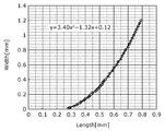
- FIG. 13 is a graph showing the relationship between the length and the width at which the parasitic inductance of the copper foil wiring is 0.35 nH.
- FIG. 14A is a cross-sectional view showing an example of the structure of the semiconductor device according to the seventh embodiment.
- FIG. 14B is a cross-sectional view showing an example of the structure of the semiconductor device according to the seventh embodiment.
- FIG. 15A is a plan view showing an example of the structure of the mounting substrate before installing the laminate and the bypass capacitor in the semiconductor device according to the eighth embodiment.
- FIG. 15B is a plan view showing an example of the structure of the semiconductor device according to the eighth embodiment.
- FIG. 15C is a plan view showing an example of the structure of the semiconductor device according to the eighth embodiment.
- FIG. 16 is a cross-sectional view and a plan view showing an example of the structure of the semiconductor device according to the ninth embodiment.
- FIG. 17 is a cross-sectional view showing an example of the structure of the semiconductor device according to the tenth embodiment.
- the minimum components required for a light source module used for distance measurement are three: a light emitting element, a switching element that controls energization of the light emitting element, and a power supply device that supplies electrical energy to these. It is widely known that power supply devices lack responsiveness to nanosecond-order pulsed high-speed responses such as high frequencies due to long wiring from the power supply device to the element, and elements that operate at high speed. A technique for ensuring high-speed response by arranging a bypass capacitor having good frequency characteristics in the immediate vicinity of the above and using this as a transient charge supply source is widely used as a conventional technique.
- the minimum components required for the light source module are elements having three types of functions: a light emitting element, a switching element, and a bypass capacitor. Elements other than the above three types may be added depending on the application, conditions, and functions.
- switching elements are often incorporated into light source modules in the form of driver ICs (semiconductor integrated circuit elements) with built-in gate driver circuits and protection functions that drive them, but elements with at least the above three types of functions are used.
- the missing light source module does not hold.
- the light emitting element, switching element, and bypass capacitor are connected in series to form a circuit, which is called a light source module as a whole.
- a circuit which is called a light source module as a whole.
- Each element is installed on a PCB (Printed Circuit Board) or a submount substrate, and each element is connected by using a metal wiring mainly formed of copper foil.
- Parasitic inductance is also generated inside each element, but it is also generated in metal wiring (hereinafter sometimes referred to simply as wiring). The longer the wiring, the larger the parasitic inductance, so it is necessary to devise ways to shorten the wiring.
- FIG. 1A schematically shows an outline of the ToF method.
- the distance [m] is calculated by the speed of light [m / s] ⁇ t tof [s] / 2.
- it is required to apply pulse energization to the light emitting element at a high cycle and control the waveform of each pulse emitted light so as to have a rectangular shape with a steep rise.
- the influence of the parasitic inductance becomes a factor that hinders the realization of an ideal rectangular waveform, so that an error occurs in the time measurement and it becomes difficult to improve the distance accuracy as shown in FIG. 1B.
- the inventors examined the structure and the configuration and arrangement of the elements having three types of functions of the light emitting element, the switching element, and the bypass capacitor, and found the necessary conditions essential for reducing the parasitic inductance. As a result, the inventors came up with the following semiconductor device (light source module).
- the semiconductor device includes a light emitting element and a semiconductor integrated circuit element including a switching element which is connected in series with the light emitting element and controls energization of the light emitting element by a control signal input from the outside.
- a hybrid type semiconductor device including the light emitting element and a bypass capacitor that supplies charge to the semiconductor integrated circuit element, the light emitting element, the semiconductor integrated circuit element, and the bypass capacitor form a power loop.
- the light emitting element and the switching element form a laminated body in which the main surfaces thereof are laminated in parallel and facing each other, and the laminated body is mounted on a mounting substrate and constitutes the laminated body.
- one electrode of the bypass capacitor is connected to the lower element.
- the other electrode is connected to the upper element and the bypass capacitor has a direction in which the inside of the bypass capacitor is directed from one electrode to the other electrode as a first direction in a plan view of the semiconductor device.
- the side of the bypass capacitor parallel to the first direction is arranged so as to have a portion parallel to and further facing one side of the outer edge of the laminate.
- the above semiconductor device is equipped with the elements required for reducing the parasitic inductance required for the light source module, it is possible to obtain pulse emitted light with a waveform closer to a rectangular shape, and it is possible to greatly improve the distance measurement accuracy.
- a hybrid type semiconductor device including a light emitting element and a discrete switching element which is connected in series with the light emitting element and has a switching function for controlling energization of the light emitting element by a control signal input from the outside. Therefore, the light emitting element and the switching element may form a laminated body in which the main surfaces thereof are laminated in parallel and facing each other.
- the above-mentioned semiconductor device can reduce the parasitic inductance generated by the connection between the light emitting element and the switching element, it is possible to obtain the pulse emitted light with a waveform close to the rectangular shape required for the light source module, and to improve the distance measurement accuracy. Can be done.
- each of the embodiments shown here shows a specific example of the present disclosure. Therefore, the numerical values, shapes, components, arrangement of components, and connection forms shown in the following embodiments are merely examples and are not intended to limit the present disclosure. Further, each figure is a schematic view and is not necessarily exactly illustrated. In each figure, substantially the same configuration is designated by the same reference numerals, and duplicate description will be omitted or simplified.
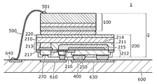
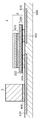
- FIG. 2A A cross section of the semiconductor device 1 according to the first embodiment is schematically shown in FIG. 2A.
- the VCSEL includes a quantum well structure 111 and a cavity structure, and emits light having a predetermined wavelength with one main surface 101 or the other main surface 102 facing back to one main surface 101 as an exit surface.
- the light emitting element 100 is installed so as to be laminated on the switching element 200, and the other main surface 102 is exposed upward as an exit surface. That is, one main surface 101 of the light emitting element 100 is in direct or indirect contact with the switching element 200 in parallel and facing the other main surface 202 of the switching element 200, and is connected in series.
- the switching element 200 in the first embodiment is mounted in contact with a PCB or a submount board 600 (hereinafter, may be commonly referred to as a mounting board).
- the mounting is performed by providing the solder bonding material 400 on the electrode pad portion of the switching element 200.
- the switching element 200 has a function of controlling energization of the light emitting element 100. That is, the emission of light from the light emitting element 100 is controlled.
- the switching element 200 is a chip size package (Chip Size Package: CSP) type discrete semiconductor in which a MOS (Metal Oxide Semiconductor) field effect transistor (Field Effect Transistor) is formed and can be mounted face-down. It is an element.
- Discrete means a semiconductor device having a single function for a single purpose.
- MOSFETs also have other functional elements such as Zener diodes formed in the same chip to protect the ESD (Electro-Static Discharge) of gate terminals. It is used only to realize stable functions as MOSFETs, and these are collectively defined as discrete MOSFETs.
- a semiconductor device having a plurality of functions and elements for a plurality of purposes is defined as an integrated circuit element.
- the switching element 200 is mainly composed of a single crystal semiconductor such as Si or a compound semiconductor such as GaN.
- the MOSFET which is the switching element 200 is a vertical trench MOSFET whose channel is in the vertical direction, and its structure is schematically shown in FIG. 2C.
- a source region 215, a source electrode (a part of 212), and a source electrode pad 250 are provided on one main surface 201 side of the switching element 200, and a gate electrode 216 and a gate electrode pad 260 are provided on the same one main surface 201.
- the switching element 200 is provided with a drain region on the other main surface 202 side facing the other main surface 201, and the drain electrode 220 is provided so as to be exposed on the other main surface 202 side.
- the drain region is composed of the semiconductor substrate 210 and the low-concentration impurity layer 211, but hereinafter, the semiconductor substrate 210 may be referred to as the drain region 210 for convenience.
- the light emitting element 100 has a structure in which the light emitting element 100 is laminated on the switching element 200 and mounted in contact with the drain electrode 220. That is, the light emitting element 100 has a structure in which the light emitting element 100 is mounted on the mounting substrate 600 via the switching element 200.
- the gate controls the current flowing from the drain region 210 to the source region 215 of the switching element 200, and when the gate of the switching element 200 is turned on by receiving a signal from the outside, the current also flows to the light emitting element 100 to emit light.
- the current flowing through the light emitting element 100 also stops, and the light emission also stops.
- 2B is a schematic plan view of a laminated structure in which a light emitting element 100 and a switching element 200 are laminated.
- the perfect circle shown by the broken line is a projection of the position of the electrode pad provided on one main surface 201 of the switching element 200.
- a laminated body only the laminated structure of the light emitting element 100 and the switching element 200 (hereinafter referred to as a laminated body) is referred to as a light source module 1.
- the current flow of the light source module 1 is as follows. At the moment when the gate of the switching element 200 is turned on, the current from the power supply positive electrode (not shown) passes through the wiring (Vin wiring 640) and the wire 500 to reach the wire bond 501 provided on the other main surface 102 of the light emitting element 100. It flows from the other main surface 102 side of the light emitting element 100 to the one main surface 101 side of the light emitting element 100 in a substantially vertical direction inside the light emitting element 100. At this time, the light emitting element 100 emits light in the quantum well structure 111 while the energization is continued, and the light is excited through the cavity structure and continues to be emitted from the other main surface 102 which is the exit surface.
- the light emitting element 100 and the switching element 200 are connected in series, and the current passing through the light emitting element 100 flows from the drain electrode 220 of the switching element 200 via the drain region 210 and the channel, and further to the source region 215 and the source electrode ( It is connected to the wiring (GND wiring 630) installed on the mounting board 600 via the source electrode pad 250 and the solder joint material 400 (a part of 212), and returns to the power supply negative electrode (strictly speaking, the power supply ground) through the wiring. This state continues as long as the gate of the switching element 200 is turned on.
- the inside of the light emitting element 100, the connection portion between the light emitting element 100 and the switching element 200, the inside of the switching element 200, and the connection portion between the switching element 200 and the mounting substrate 600 a parasitic inductance is generated in the wire 500 connecting the power supply and the light emitting element 100 and the wiring provided in the mounting board 600. If there is a conduction path through which current flows, a parasitic inductance will occur there. It is called parasitic inductance because it is an inductance that is difficult to avoid in a form that is not intended in circuit design. The parasitic inductance has a great influence on the light emission responsiveness of the semiconductor device (light source module) 1, and it is essential to reduce the parasitic inductance in order to improve the distance measurement accuracy as the light source module.
- the physical path through which the current conducts in the entire semiconductor device (light source module) 1 may be shortened.
- the conduction path is the light emitting element. From the in-in to the other main surface 102 side, which is the exit surface of 100, to the out to the mounting substrate 600 of the switching element 200, it is carried out in a substantially linear and shortest path. Therefore, in principle, the parasitic inductance provided between the light emitting element 100 and the switching element 200 is the most reduced.
- FIG. 3 schematically shows a conventional horizontal configuration as Comparative Example 1.
- the light emitting element 100 and the switching element 200 are not laminated as in the first embodiment, but are individually mounted on the mounting substrate 600 and then connected by wiring (as shown in FIG. 3). Wiring is not shown in FIG. 3). Even if the light emitting element 100 and the switching element 200 are installed close to each other, they need to be connected by wiring, and a parasitic inductance is generated by the length thereof. Further, the light emitting element 100 is often commercialized as a packaged product mounted on a submount substrate as a general commercial product, and when these are used, the wiring from the light emitting element 100 to the outer shape of the package becomes extra long.
- the connection distance is the shortest
- the conduction path inside the light emitting element 100 and the switching element 200 is also the thickness of each element. Since it is equivalent to, it is clear that it is the shortest path in which no extra conduction path is eliminated.
- FIG. 4 light is emitted from the light emitting element 100 when the switching element 200 is pulse-energized in the arrangement shown in the first embodiment ((a) in FIG. 4) and the comparative example 1 ((b) in FIG. 4).
- the waveforms are shown in layers. (C) of FIG. 4 will be described later.
- the distance between the light emitting element 100 and the switching element 200 can be minimized by stacking the light emitting element 100 and the switching element 200, so that the effect of reducing the parasitic inductance caused by the wiring can be reduced. Can be obtained.
- the switching element 200 is a vertical trench MOSFET that conducts a current in the vertical direction, the conduction path inside the switching element 200 can be minimized, so that the effect of reducing the parasitic inductance inside the switching element 200 is obtained. Be done. As a result, the parasitic inductance can be reduced to 1.0 nH, and the rise can be greatly improved as shown in FIG. 4 (a).
- the distance measurement accuracy of the semiconductor device (light source module) 1 improves as the waveform has a rectangular shape with a steeper rise. Furthermore, the output peak (waveform height) can be improved by the steep rise, and the effect of improving the distance measurement accuracy and increasing the sensing distance by the higher peak can be expected.
- the switching element 200 is described as a vertical trench MOSFET, but the effect of the invention can be obtained even with a horizontal MOSFET.
- Horizontal MOSFETs include, for example, planar type and LDMOS (Laterary Diffused MOSFET).
- a drain drawer region connected to the drain region 210 is formed on one main surface 201 side of the switching element 200, and a horizontal channel is formed between the drain drawer region and the source region 215 formed on the same one main surface 201 side.
- the gate electrode 216 may be installed via the insulating film 217. With such a structure, the horizontal MOSFET can be used as the switching element 200 while the other main surface 202 side of the switching element 200 is covered with the drain electrode 220.
- the effect of reducing the parasitic inductance inside the switching element 200 is reduced by the amount of the horizontal channel as compared with the case of using the vertical trench MOSFET, but the capacitance (charge amount Qg) associated with the gate structure is reduced. It is significant to enhance the responsiveness because it can suppress.
- the switching element 200 is installed as a lower element mounted on the mounting substrate 600, and the light emitting element 100 is mounted above the switching element 200 which is the lower element. It is assumed that the laminated body 2 as an upper element is provided. However, it may be a laminate in which the light emitting element is the lower element and the switching element is the upper element. Since the light emitting element 100 and the switching element 200 forming the laminate 2 in the semiconductor device (light source module) 1 do not need to use wiring for connecting both elements regardless of which is the lower element or which is the upper element. It remains effective in reducing parasitic inductance.
- the light emitted from the light emitting element 100 is almost emitted from the exit surface which is the other main surface 202, but a part of the light is emitted from the surface other than the emission surface (one main surface 201 or the side surface). Leak.
- the semiconductor device (light source module) 1 it is desirable to collect and effectively utilize the luminous light leaking from the surface other than the emitting surface. Therefore, when the semiconductor device (light source module) 1 is viewed in a plan view, a region wider than the area of the light emitting device 100 is included so that the light emitting element 100 can be included at least in a region immediately below the light emitting element 100, preferably in a plan view.
- the drain electrode 220 can be provided so as to be exposed on the other main surface 202, so that the above structure can be realized. Is easy.
- the drain electrode 220 of the switching element 200 is provided with at least a metal layer containing silver (Ag) or copper (Cu) having high reflectance as a component, this effect is further desirable. Further, the drain electrode 220 of the switching element 200 may be formed on the entire surface of the other main surface 202 of the switching element 200. With such a configuration, the light emitted from the surface of the light emitting element 100 that is not the emitting surface is reflected to the emitting surface side in a wide range, and the semiconductor device (light source module) 1 can exhibit good luminous efficiency.
- the light emitting element 100 and the switching element 200 are independent elements that function individually, and have a structure in which these are combined in a hybrid and laminated. That is, the light emitting element 100 and the switching element 200 must be connected in series in some way.
- connection method Metal joining is desirable as the connection method.
- the one main surface 101 side of the light emitting element 100 and the other main surface 202 side of the switching element 200 are aligned in parallel and facing each other, and the electrode metals provided on the respective surfaces are brought into contact with each other to perform the joining process.
- There are various methods for the joining treatment and ultrasonic waves may be used, pressure application, heat treatment, or a combination thereof may be carried out. It is required to appropriately select the electrode metal provided on one main surface 101 of the light emitting element 100 and the metal constituting the drain electrode 220 of the switching element 200 according to each bonding method.
- connection between the light emitting element 100 and the switching element 200 does not generate an extra length of the conduction path as compared with the case where an indirect material is additionally used, so that it is the most from the viewpoint of reducing parasitic inductance. desirable.
- FIG. 2A schematically shows a structure in which both elements are connected by using the adhesive member 300.
- the conductive adhesive member 300 include Ag paste and sintered silver.
- the space between the light emitting element 100 and the switching element 200 is filled without gaps. If a gap is generated or the area where the adhesive member 300 is not filled becomes large, the adhesive force between the light emitting element 100 and the switching element 200 becomes insufficient, the strength of the semiconductor device 1 becomes insufficient, and the reliability becomes high. It is likely to lead to a decline. Therefore, when the adhesive member 300 is used, when the semiconductor device 1 is viewed in a plan view, the area where the adhesive member 300 is installed is controlled so as to slightly exceed the area where the light emitting element 100 and the switching element 200 overlap. Is desirable.
- the adhesive member 300 extends outward on at least one of the four sides of the outer edge of the light emitting element 100. If such a stretched portion is seen, it can be said that the adhesive strength between the light emitting element 100 and the switching element 200 is sufficient, and it is unlikely that the reliability will be lowered.
- a protrusion structure is provided on the outer edge of the other main surface 202 on which the drain electrode 220 of the switching element 200, which is the lower element, is formed, from the lower side to the upper side of the laminated body 2, and the adhesive member 300 does not spill from the switching element 200. It is effective to have the function of a barrier.
- the above-mentioned protrusion structure is effective even if it is formed along at least one of the four sides of the outer edge of the other main surface 202 on which the drain electrode 220 of the switching element 200 is formed.
- FIG. 5 shows an example of a protrusion structure.
- the protrusion structure may prevent the adhesive member 300 from sticking out. As shown in FIG. 5, it may be composed of only the metal forming the drain electrode 220, or may be composed of the semiconductor substrate 210 and the drain electrode 220 in combination. It is desirable that the height of the protrusion structure does not exceed the height (thickness) of the light emitting element 100. This is because if the height of the protrusion structure is equal to or less than the height of the light emitting element 100, the possibility that the wire 500 connecting the Vin wiring 640 and the emission surface of the light emitting element 100 will come into contact with the protrusion structure is reduced.
- the conductive adhesive member 300 may be selectively installed only in a predetermined area. In this case, the effect of relaxing the stress generated by laminating and mounting the light emitting element 100 and the switching element 200 can be expected. Further, when it is desired to seal between the two elements with a sealing material such as resin, there is an effect that the sealing material is evenly penetrated to facilitate filling by providing a space between the two elements to some extent.
- the light emitting element 100 and the switching element 200 are each mounted by some procedure.
- the conduction cross-sectional area increases from the upper element to the lower element. If there is a place where the conduction cross-sectional area becomes narrow when flowing from above to below, it becomes difficult to cope with large current energization due to an increase in resistance, and the heat dissipation path is narrowed down, so that the semiconductor device 1 itself becomes hot. This is because it is easy to change. Therefore, it is desirable to adjust the area of both elements and the region where the current flows so that the current density of the lower element becomes smaller than the current density of the upper element when the laminated body 2 is energized. In order to realize these, it is desirable that the area of the lower element is larger than the area of the upper element in the lower element and the upper element.
- both of the mounting methods (A) and (B) there is a process of laminating the upper element on the upper surface of the lower element and mounting the upper element. If the area of the upper element is larger, the lower element cannot be visually recognized at the stage of stacking, and mounting tends to be difficult especially from the viewpoint of alignment. Further, in terms of ease of manufacturing the laminate, that is, ease of mounting, it is desirable that both the light emitting element 100 and the switching element 200 have a rectangular shape. If both elements have a rectangular shape in a plan view, it is easy to align the four sides of the outer edge of the upper element with the four sides of the outer edge of the lower element so that they are parallel to each other when manufacturing the laminate. be.
- the upper element is laminated. It is possible to reduce the possibility that the upper element protrudes from the lower element to form a laminated body that overhangs.
- the outer edge of the laminated body when viewed in a plan view refers to the outer edge of the outermost element at each position regardless of the relationship between the area and arrangement of the upper element and the lower element.
- both the light emitting element 100 and the switching element 200 have a rectangular shape, it is desirable that the four sides of the outer edge of the upper element are parallel to the four sides of the outer edge of the corresponding lower element in a plan view. Further, it is desirable to configure the laminated body 2 in an arrangement in which the centers of both elements coincide with each other. At this time, when the laminated body 2 is manufactured, the external force received by the laminated body 2 and the stress generated in the laminated body 2 can be symmetrically dispersed over the entire laminated body 2. Since it is easy to prevent the occurrence of a place where external force and stress are locally concentrated, the possibility that the laminated body 2 is physically destroyed can be reduced.
- both the light emitting element 100 and the switching element 200 have a rectangular shape, it is desirable that the four sides of the outer edge of the upper element are parallel to the four sides of the outer edge of the corresponding lower element in a plan view. At least one of the four sides of the outer edges of both elements may overlap in a plan view, or may be biased toward one side. At this time, in a plan view, the exposed area of the upper surface of the lower element that is not covered by the upper element can be secured to some extent.
- An electrode pad for the lower element may be installed in this portion, or a visible mark that can identify the laminated body 2 or the lower element may be formed. In the case of mark formation, it is convenient because the source of the lower element can be identified even after the laminated body 2 is formed.
- both the light emitting element 100 and the switching element 200 have a rectangular shape, the four outer edges of the upper element do not necessarily have a parallel relationship with the four outer edges of the corresponding lower elements in a plan view. good.
- the wire 500 can be arranged to be shortened as much as possible due to the positional relationship with the wiring provided on the mounting substrate 600.
- some alignment mark indicating the position where the upper element is mounted may be installed on the upper surface of the lower element.
- the difference between the second embodiment and the first embodiment is that the switching element 200 is a horizontal MOSFET having a horizontal channel.
- the switching element 200 includes a drain electrode 220 and a drain region 210, and further includes a drain drawer region 213 that is electrically connected to the drain region 210 on one main surface 201 side.
- a well layer 214 and a source region 215 are formed on one main surface 201 side, and the space between the well layer 214 and the drain drawer region 213 corresponds to a horizontal channel.
- the gate electrode 216 is in contact with the well layer 214 and a part of the low-concentration impurity layer 211 via the insulating film 217, and when the voltage applied to the gate electrode 216 in response to an external signal exceeds the threshold value, A horizontal channel is formed in the well layer 214 in contact with the gate electrode 216, and a current flows.
- the current flow of the semiconductor device (light source module) 1 in the second embodiment is as follows. At the moment when the gate of the switching element 200 is turned on, the current from the power supply positive electrode (not shown) passes through the wiring (Vin wiring 640) and the wire 500 to reach the wire bond 501 provided on the other main surface 102 of the light emitting element 100. It flows from the other main surface 102 side of the light emitting element 100 to the one main surface 101 side of the light emitting element 100 in a substantially vertical direction inside the light emitting element 100. At this time, the light emitting element 100 emits light in the quantum well structure 111 while the energization continues, and the emitted light is excited through the cavity structure and continues to be emitted from the other main surface 102 which is the exit surface.
- the light emitting element 100 and the switching element 200 are connected in series, and the current passing through the light emitting element 100 passes from the drain electrode 220 of the switching element 200 via the drain region 210, the drain extraction region 213, and the horizontal channel. Further, the source region 215, the source electrode (a part of 212), the source electrode pad 250, and the solder joint material 400 are connected in this order to the wiring (GND wiring 630) installed on the mounting board 600, and the power supply negative electrode (strictly speaking) is passed through the wiring. Return to power ground). This state continues as long as the gate of the switching element 200 is turned on.
- the conduction path inside the switching element 200 becomes slightly longer than that using the vertical trench MOSFET as shown in the first embodiment. Therefore, it is widely known that the horizontal MOSFET has a lower gate capacitance (charge amount Qg) associated with the gate structure than the vertical trench MOSFET, although the effect of reducing the parasitic inductance in the switching element 200 is reduced by that amount. Therefore, the switching speed of the MOSFET can be made faster than that of the vertical trench MOSFET, which is significant in improving the responsiveness as a result.
- a drain electrode and a drain electrode pad 270 can be provided on one main surface 201 side as well. Since it is not essential for the semiconductor device (light source module) in the present invention to include the drain electrode pad 270, the drain electrode pad 270 does not have to be connected to the wiring via the solder joint material 400. However, a drain electrode pad 270 is also provided on one main surface 201 side, and by further connecting to a wiring for inspection of a semiconductor device, for example, the function of the semiconductor device being manufactured can be evaluated correctly, which is meaningful for some purposes. It can also be used.
- the switching element 200 is a horizontal MOSFET having a horizontal channel.
- the mounting substrate 600 has a step, the light emitting element 100 is installed on the lower side of the step, the switching element 200 is installed on the upper side of the step, and the light emitting element 100 and the switching element 200 are only partially in plan view. Is laminated.
- the portion where the light emitting element 100 and the switching element 200 are laminated in a plan view is called a laminated body.
- the laminated body 2 in the third embodiment corresponds to the portion shown by the broken line in FIG.
- the current flow of the semiconductor device (light source module) 1 in the third embodiment is as follows. At the moment when the gate of the switching element 200 is turned on, a current flows from a power supply positive electrode (not shown) to one main surface 101 of the light emitting element 100 through a Vin wiring 640 provided on the mounting substrate 600, and further, the other main surface of the light emitting element 100. It flows substantially vertically inside the light emitting element 100 toward the surface 102 side. At this time, the light emitting element 100 emits light in the quantum well structure 111 while the energization is continued, and the light is excited through the cavity structure and continues to be emitted from the other main surface 102 which is the exit surface.
- the light emitting element 100 and the switching element 200 are connected in series in a part of the stack, and the current passing through the light emitting element 100 passes from the drain electrode 220 of the switching element 200 via the high concentration impurity region 218 and the horizontal channel. Then, the source region 215, the source electrode (a part of 212), the source electrode pad 250, and the solder joint material 400 are connected in this order to the wiring (GND wiring 630) installed on the mounting board 600, and the power supply negative electrode is passed through the wiring. Return to. This state continues as long as the gate of the switching element 200 is turned on.
- the light emitting element 100 and the switching element 200 are only partially laminated, and there is no extra wiring in the conduction path, so that the effect of reducing the parasitic inductance of the connecting portion can be obtained.
- the light emitting element 100 and the switching element 200 are only partially laminated, and there is no extra wiring in the conduction path, so that the effect of reducing the parasitic inductance of the connecting portion can be obtained.
- an opening portion is provided only in the portion directly below the light emitting element 100 in the mounting substrate 600. is necessary.
- the switching element 200 in the third embodiment needs to be provided with a drain electrode 220 on one main surface 201 side, and further to be provided with a drain electrode pad 270. On the other hand, it is not necessary to provide the drain electrode 220 on the other main surface 202 side of the switching element 200. Further, unlike the second embodiment, it is not necessary to provide a drain drawer region 213 electrically connected to the drain region 210 on one main surface 201 side. It is common that the well layer 214 and the source region 215 are formed on the one main surface 201 side, and the space between the source region 215 and the high-concentration impurity region 218 corresponds to a horizontal channel.
- the gate electrode 216 is in contact with a part of the well layer 214 via the insulating film 217, and when the voltage applied to the gate electrode 216 in response to an external signal exceeds the threshold value, the well in which the gate electrode 216 is in contact.
- a horizontal channel is formed in the layer 214 and a part of the low-concentration impurity layer 211, and a current flows.
- the mounting substrate 600 has a step, and the light emitting element 100 and the switching element 200 are installed on the lower side and the upper side of the step so as to partially overlap each other.
- the light emitting element 100 is not limited to the lower side and the switching element 200 is not limited to the upper side.
- the light emitting element 100 may be on the upper stage side, and the switching element 200 may be on the lower stage side.
- the height of the step of the mounting substrate 600 should be about the same as the height (thickness) of the element installed on the lower stage side so that the light emitting element 100 and the switching element 200 can be easily laminated even in a part. Is desirable.
- it is more desirable that the other main surface of the lower element mounted on the lower side is aligned with the same height as the upper side of the mounting substrate.
- the switching elements 200 shown in the first to third embodiments are discrete MOSFETs that form a laminate 2 with the light emitting element 100.
- the first embodiment shows a vertical trench MOSFET, and the second and third embodiments show a horizontal MOSFET.
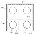
- FIG. 8A is a schematic view when viewed in a plan view from one main surface 201 side of the discrete MOSFET which is the switching element 200.
- the MOSFET includes an effective region 255 provided with a channel and a source electrode pad 250 corresponding to an opening of the source electrode.
- the effective region 255 occupies about half the region of the MOSFET, and two of the four round electrode pads are the source electrode pads 250.
- a control region 265 having one gate electrode pad 260 and a drain drawer region 275 having one drain electrode pad 270 are arranged in a portion other than the effective region 255.
- the outer edge portion of the MOSFET is provided with a non-functional region 280 that does not correspond to any of the effective region 255, the control region 265, and the drain extraction region 275.
- the shape of the electrode pad is shown as a perfect circle, but the shape is not limited to this, and may be elliptical or rectangular, and the end is not only circular but also rectangular. Or it may have a polygonal shape. Further, all the electrode pads may or may not have the same shape.
- the responsiveness of light emitted from the light emitting element 100 is important.
- the switching element 200 is a MOSFET
- widening the effective region 255 provided with the channel is effective in facilitating the energization of a large current due to the low resistance, but as a side effect, the gate capacitance associated with the gate structure ( The amount of charge Qg) also increases.
- the above-mentioned parasitic inductance is dominant in the responsiveness of the switching element, but the gate capacitance and the influence occur in the MOSFET.
- the switching element (MOSFET) 200 having a large gate capacitance has a reduced on / off responsiveness due to the gate drive, which leads to a decrease in the light emission responsiveness of the light emitting element 100. Therefore, the switching element (MOSFET) 200 takes into consideration the amount of current, resistance, responsiveness, etc. required for the semiconductor device (light source module) 1, and further considers the ease of mounting when forming the laminate 2 together with the light emitting element 100. And you have to select the area.
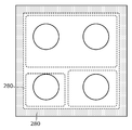
- the area of the lower element is larger than the area of the upper element in any mounting method of the semiconductor device (light source module) 1. Therefore, increasing the area of the switching element (MOSFET) 200 significantly affects the ease of mounting, but if the effective region is expanded accordingly, the responsiveness is impaired. Therefore, as shown in FIG. 8B, the area of the effective region 255 that satisfies the current amount, resistance, and responsiveness required for the semiconductor device (light source module) 1, the area of the control region 265, and the area of the drain extraction region 275 are fixed. As it is, it is beneficial to realize the area of the switching element (MOSFET) 200 by expanding the non-functional area in order to ensure the ease of manufacturing the laminated body 2. As shown in FIG.
- the four sides of the outer edge of the switching element (MOSFET) 200 are uniformly enlarged in plan view to form the effective region 255, the control region 265, and the drain extraction region 275. It is effective to expand the non-functional area 280 which does not correspond to any of them. Regarding the expansion of the area, it is desirable to control the diagonal length of the upper element to be smaller than the short side length of the lower element.
- FIG. 8A may be a MOSFET as shown in FIG. 8C.
- a switching element (MOSFET) 200 having an increased area, that is, an effective region 255, as shown in FIG. 8C.
- FIG. 8C includes all round electrode pads of the same size, and one gate electrode pad 260 and control area 265, 2 except for the non-functional region 280 provided on the outer edge portion.
- the effective region 255 is other than the two drain electrode pads 270 and the drain drawer region 275.
- six source electrode pads 250 are provided inside the effective region 255.
- FIG. 9A shows an example of an equivalent circuit relating to the semiconductor device (light source module) 1.
- the laminate 2 in which the light emitting element 100 and the discrete switching element 200 are laminated has been illustrated, but the semiconductor device (light source module) 1 according to the fifth embodiment includes the switching element 200, and further comprises the switching element 200.
- a semiconductor integrated circuit element (driver IC) 700 having a built-in gate driver circuit for driving the above is mounted.
- the semiconductor integrated circuit element (driver IC) 700 may include other functional circuits of the gate driver circuit.
- a general analog control circuit for adding additional functions such as an overheat protection circuit, an overcurrent detection circuit, and a step-down regulator circuit may be included.
- FIG. 9B shows a schematic view of the semiconductor integrated circuit element (driver IC) 700 in a plan view.
- the semiconductor integrated circuit element (driver IC) 700 has a switching element 200 and a gate driver circuit 710 monolithically formed on the same chip, and is in the form of a chip size package.
- the gate driver circuit 710 is formed on the left side of the chip, and the switching element 200 is formed on the right side.
- both the switching element 200 portion and the gate driver circuit 710 portion are provided with a perfect circular electrode pad having the same size. Each electrode pad may be connected to a different function, and some of them may be connected to the same function.
- the switching elements may be configured in a plurality of parallel configurations.
- FIG. 9C shows a schematic cross-sectional structure of the semiconductor integrated circuit element (driver IC) 700.
- the gate driver circuit 710 is formed by forming a digging structure in the low-concentration impurity region 211 by dry etching or the like, covering the entire surface with an insulating film 217, and then performing epitaxial growth or impurity doping. This is because the potentials of the drain region (semiconductor substrate) 210 and the low-concentration impurity region 211 become the drain voltage and are not zero volt, so that insulation from the substrate side is required for stable operation of the control circuit.
- the switching element 200 is described as a vertical trench MOSFET in FIG. 9C, it may be a horizontal MOSFET.
- the switching element 200 built in the semiconductor integrated circuit element (driver IC) 700 is a vertical trench MOSFET, and the light emitting element 100 is laminated so as to be mounted on the vertical trench MOSFET portion so as to overlap even a part thereof. It is preferable to form the body 2. At this time, the same as shown in FIG. 2A, the conduction path inside the laminated body 2 can be minimized, so that the effect of reducing the parasitic inductance can be expected.
- switching element can be read as the semiconductor integrated circuit element described in the fifth embodiment unless it is limited to a discrete element. It is also possible to use the technique described in the fourth embodiment for a semiconductor integrated circuit element.
- the semiconductor device 1 in the sixth embodiment includes a bypass capacitor 3 in addition to the light emitting element 100 and the switching element 200 forming the laminated body 2.
- the bypass capacitor 3 is connected in series with the laminated body 2 and plays a role of supplying electric charges to the laminated body 2. Therefore, the bypass capacitor 3 is an indispensable element for the semiconductor device (light source module) 1 to function. More specifically, one electrode 32 of the bypass capacitor 3 is connected to the lower element forming the laminate 2, and the other electrode 31 is connected to the upper element forming the laminate 2, so that the bypass capacitor 3 and the light emitting element 100 are connected.
- the switching element 200 forms a power loop.
- the power loop referred to in the present application is a bypass capacitor 3 that passes through the laminate 2 from a terminal (the other electrode 31 or one electrode 32) corresponding to the positive electrode when the power supply of the bypass capacitor 3 is energized, without being electrically interrupted. It is a conduction path in which a current flows in one way to a terminal (one electrode 32 or the other electrode 31 or a power supply ground) corresponding to the negative electrode when the power supply is energized. It should be noted that it is a conduction path through which a large current of about ampere order, which is required to obtain a desired light output of a light emitting element, is passed as compared with a minute current consumed by a control circuit or the like. ..
- this conduction path may be referred to as a power loop.
- the bypass capacitor 3 it is desirable to use a chip type multilayer ceramic capacitor having a small internal parasitic inductance and good high-speed response.
- the bypass capacitor 3 is inherently provided in each of the embodiments.
- the bypass capacitor 3 is provided, and the features of the laminate 2 and the bypass capacitor 3 are described.
- the lower element is the switching element 200 and the upper element is the light emitting element 100. Further, both the light emitting element 100 and the switching element 200 have a rectangular shape. Further, the lower element is described on the premise of the discrete switching element 200, but the present invention is not limited to this, and the semiconductor integrated circuit element 700 including the switching element may be used.
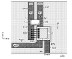
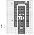
- FIG. 10A is an example of the mounting board 600 before mounting the laminate 2 and the bypass capacitor 3.
- the four perfect circles indicate the planned installation positions of the electrode pads when the switching element 200 is mounted face-down.
- Metal wirings 610, 620, 630, and 640 that perform their respective functions are installed on the mounting board 600.
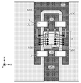
- FIG. 10B illustrates a state when the laminated body 2 and the bypass capacitor 3 are mounted.
- One electrode 32 of the bypass capacitor 3 is connected to the GND wiring 630, and the source electrode pad 250 of the switching element 200, which is a lower element of the laminate 2, is connected to the GND wiring 630.
- the other electrode 31 of the bypass capacitor 3 is connected to the Vin wiring 640, and the wire 500 connects the Vin wiring 640 to the upper surface of the light emitting element 100 which is an upper element of the laminate 2.
- a solder joint material 400 is used to connect the source electrode pad 250 and the GND wiring 630.
- One end of the gate wiring 610 is connected to the gate electrode pad 260 of the switching element 200, which is the lower element of the laminate 2, via the solder joint material 400.
- the other end of the gate wiring 610 is connected to a gate driver (not shown) that controls ON / OFF of the switching element 200.
- the gate driver gives the switching element 200 an ON / OFF signal having sufficient source current and sink current capability to drive the switching element 200 at high speed in response to a signal input from the outside.
- the wiring 620 is a drain wiring connected to the drain electrode pad 270 of the switching element 200 via the solder bonding material 400.
- the switching element 200 of the sixth embodiment includes the drain electrode pad 270 on one main surface 201 side, the drain electrode pad 270 does not necessarily have to be installed. Instead of the drain electrode pad 270, a source electrode pad 250 may be formed and arranged to connect to the GND wiring 630.
- the bypass capacitor 3 when the bypass capacitor 3 is viewed in a plan view and the direction in which the inside of the bypass capacitor 3 is directed from one electrode 32 to the other electrode 31 is the first direction, the side parallel to the first direction of the bypass capacitor 3 is formed.
- the laminated body 2 is installed so as to have a portion parallel and facing one side of the outer edge. This arrangement plays an important role in reducing parasitic inductance.
- the direction in which the laminate 2 and the bypass capacitor 3 are parallel to the first direction in a plan view is defined as the x direction
- the direction orthogonal to the x direction is the direction in which the laminate 2 and the bypass capacitor 3 are arranged side by side. Is set as the y direction.
- the direction of bridging the Vin wiring 640 and the GND wiring 630 is the x direction
- the direction parallel to the Vin wiring 640 and the GND wiring 630 is the y direction.
- the first direction is defined by paying attention to one bypass capacitor 3 in a plan view, and when a plurality of bypass capacitors 3 are provided, the first direction is defined for each of the provided bypass capacitors 3. Will be done.
- the x-direction and the y-direction are directions defined by paying attention to the arrangement relationship of one laminate 2 and one bypass capacitor 3 in a plan view, and when a plurality of bypass capacitors 3 are provided, they are provided.
- the x-direction and the y-direction are defined for each of the bypass capacitors 3.
- the first direction and the x direction are generally the same.
- the current flow in the sixth embodiment is as follows.
- a gate drive signal from a gate driver (not shown) at the connection destination of the gate wiring 610
- an electric charge is charged from the other electrode 31 (corresponding to the positive electrode when energized) of the bypass capacitor 3. It is supplied and current flows.
- a current flows from the other electrode 31 of the bypass capacitor 3 (corresponding to the positive electrode when energized) to the Vin wiring 640, the wire 500, and the light emitting element 100, leading to the emission of light from the light emitting element 100.
- the energization continues, that is, while the gate of the switching element 200 is on, the light emitted from the light emitting element 100 continues to be emitted.
- the current is further passed from the light emitting element 100 through the switching element 200, the source electrode pad 250 of the switching element 200, and the GND wiring 630, and one electrode 32 of the bypass capacitor 3 (connected to the power supply ground, which corresponds to the negative electrode when energized).
- the internal path of the laminated body 2 is as described in the first to third embodiments, but in the sixth embodiment, the path connecting the bypass capacitor 3 and the laminated body 2 will be described.
- a typical size is assumed as a small light source module.
- the light emitting element 100 is 1.0 ⁇ 1.0 mm
- the switching element 200 is a discrete vertical trench MOSFET of 1.4 ⁇ 1.4 mm
- the bypass capacitor 3 is The one of 1.0 ⁇ 0.5 mm is shown.
- the switching element 200 is provided with two circular source electrode pads 250 on one main surface 201 side, one circular gate electrode pad 260 and one drain electrode pad 270, respectively, and the other main surface 202. The entire side is covered with the drain electrode 220.
- the characteristics of the light emitting element 100 and the shape and size of the element are selected according to the required light output and characteristics, and the required amount of current and responsiveness, and the ease of mounting as a lower element on which the light emitting elements 100 can be laminated, etc.
- the characteristics of the switching element 200 and the shape and size of the element are selected in consideration of the above. Further, a desirable capacitance value, size, and shape of the bypass capacitor 3 are selected according to the required current amount and responsiveness.
- FIG. 10B shows a typical element size that satisfies these correlations as a small light source module.
- the thickness is relatively shown according to the actual size. That is, the thickness of the light emitting element 100 is 0.1 to 0.2 mm, the thickness of the switching element 200 is about 0.1 mm, the thickness of the laminated body 2 is 0.3 to 0.4 mm, and the height of the bypass capacitor 3 is high. Is about 0.5 mm.
- the wire 500 connecting the Vin wiring 640 and the GND wiring 630 is not limited to the height of the laminate 2. It is necessary to have a length corresponding to at least the wiring interval. Since the bypass capacitor 3 straddles the same Vin wiring 640 and the GND wiring 630, the length of the side parallel to the first direction of the bypass capacitor 3 at least in a plan view is longer than the wiring interval between the Vin wiring 640 and the GND wiring 630. It is necessary. Further, it is desirable that the bypass capacitor 3 is arranged so that the side parallel to the first direction in the plan view is parallel to one side of the outer edge of the laminated body 2.
- FIG. 10D shows an arrangement in which the bypass capacitor 3 is rotated by 45 ° with respect to the laminated body 2 in FIG. 10B.
- the bypass capacitor represented by the broken line in FIG. 10D indicates the position in FIG. 10B before rotation, and the x-direction and the y-direction in FIG. 10D indicate the arrangement of the bypass capacitor and the laminate 2 represented by the broken line. Define based on relationships. Since the bypass capacitor 3 and the laminate 2 need to be arranged at a minimum distance to prevent a short circuit, if this is provided in the same amount as in the case of FIG. 10B, the other electrode 31 of the bypass capacitor 3 and the wire 500 are provided.
- the distance between the Vin wirings 640 in the y direction can be shortened to a certain extent (- ⁇ y1 in FIG. 10D), but the Y direction of the GND wiring 630 between one electrode 32 of the bypass capacitor 3 and the laminate 2
- the distance of is greatly expanded as compared with the case of FIG. 10B (+ ⁇ y2 in FIG. 10D), and the total length of the power loop in the y direction increases (+ ⁇ y2- ⁇ y1> 0). Therefore, it is desirable that the bypass capacitor 3 is arranged so that the side parallel to the first direction in the plan view is parallel to one side of the outer edge of the laminated body 2.
- the bypass capacitor 3 is arranged so that the side parallel to the first direction has a portion facing one side of the outer edge of the laminated body 2 in a plan view. This is the same as the fact that when the cross section of the semiconductor device 1 is viewed along the y direction as shown in FIG. 10C, there is a place where the laminate 2 and the bypass capacitor 3 are provided in the same cross section.
- FIG. 10C is a cross-sectional view of the portion shown by the alternate long and short dash line in FIG. 10B.
- FIG. 10E shows an example in which the side parallel to the first direction of the bypass capacitor 3 is arranged so that there is no portion facing one side of the outer edge of the laminated body 2 in a plan view.
- the bypass capacitor shown by the broken line in FIG. 10E indicates the position of the bypass capacitor 3 shown in FIG. 10B with respect to the laminated body 2.
- the distance between the bypass capacitor 3 and the laminate 2 along the x direction is widened, and the wire 500 also needs to be lengthened (+ ⁇ x).
- the total length increases (+ ⁇ x + ⁇ x> 0). Therefore, it is desirable that the bypass capacitor 3 is arranged so that the side parallel to the first direction has a portion facing one side of the outer edge of the laminated body 2 in a plan view.
- the bypass capacitor 3 divides the side parallel to the first direction into a part 320 including one electrode 32 and another part 310 including the other electrode 31, and the part 320 is a laminated body.
- the other portion 310 is arranged so as to have a portion facing one side of the outer edge of 2 and not facing one side of the outer edge of the laminated body 2 but having a portion facing an extension line of this one side. Is desirable.
- the bypass capacitor 3 has two sides parallel to the first direction as shown in FIG. 10B. It is desirable that the equally divided part 320 including one electrode 32 is arranged so as to face one side of the outer edge of the laminated body 2. With such an arrangement, the power loop in the x direction can be shortened without making an unreasonable wiring design.
- the other portion 310 including the other electrode 31, which is obtained by dividing the side parallel to the first direction of the bypass capacitor 3 into two equal parts, does not face one side of the outer edge of the laminate 2. This is because such an arrangement has the effect of shortening the connection path between the other electrode 31 of the bypass capacitor 3 and the upper element of the laminate 2.
- the bypass capacitor 3 is laminated from the other electrode 31 (corresponding to the positive electrode when energized).
- the installation position and direction of the wire 500 are more important. be.
- the wiring In order to drive down the wire 500 onto the wiring on the mounting board, it is required that the wiring has a sufficient width in consideration of the variation in the position of the wire bonding. Therefore, in FIGS. 10B and 11A, it is difficult to lower the wire 500 to the position sandwiched between the laminate 2 and the bypass capacitor 3 (that is, to lower the wire 500 in the y direction). Therefore, it is efficient in mounting work that the wire 500 is taken down in the direction in which the bypass capacitor 3 is not installed with respect to the laminated body 2. Then, the wire bond 501 is installed along one side of the outer edge of the light emitting element 100 in a plan view, which is closer to the other electrode 31 of the bypass capacitor 3 among the sides in the direction orthogonal to the first direction. It is desirable to be done. Further, it is preferable that the wire 500 is driven down to the Vin wiring 640 in parallel with the first direction in a plan view.
- the light emitting element 100 and the switching element 200 forming the laminated body 2 are both rectangular in a plan view, and the corresponding outer edges are arranged so as to be parallel to each other. Even if the light emitting element 100, which is the upper element, is biasedly installed on the upper surface of the switching element 200, which is the lower element, at a position close to the other electrode 31 side of the bypass capacitor 3 along the first direction. good.
- the light emitting element 100 is installed on the upper surface of the switching element 200 so as to be biased in the ⁇ y direction.
- FIG. 11B The arrangement as shown in FIG. 11B can also be selected.
- the bypass capacitor 3 is arranged so that the side parallel to the first direction is parallel to one side of the outer edge of the laminated body 2 and faces the entire length of the bypass capacitor 3 in a plan view.
- the portion of the power loop parallel to the first direction can be shortened as much as possible in a plan view. If the length of one side of the outer edge of the laminated body 2 is longer than the length of the side parallel to the first direction of the bypass capacitor 3 in a plan view, it is desirable to select the arrangement as shown in FIG. 11B.
- the wire bond 501 at this time is the corner portion closest to the other electrode 31 of the bypass capacitor 3 among the four corner portions in the plan view on the upper surface of the light emitting element 100 which is the upper element of the laminated body 2. It is desirable to install it in the vicinity of. Further, it is preferable that the wire 500 is driven down to the Vin wiring 640 in a direction forming about 45 ° with the first direction in a plan view.
- the angle formed by the wire 500 and the first direction in a plan view is not limited to 45 °. What is important is to shorten the power loop for wiring by arranging the wire 500 toward the other electrode 31 of the bypass capacitor 3. At this time, the angle formed by one or more wires 500 and the first direction may be larger than 0 ° and smaller than 90 °.
- FIG. 11C The arrangement as shown in FIG. 11C can also be selected.
- the installation direction of the light emitting element 100, which is the upper element is rotated by 45 ° with respect to the switching element 200, which is the lower element, as compared with FIG. 11B.
- the switching element 200 which is the lower element
- FIG. 11C the margin when the upper element is mounted on the upper surface of the lower element is smaller than that in the case where the outer edge of the lower element and the outer edge of the upper element are installed in parallel in a plan view (FIG. 11B).
- the area of the lower element may be slightly increased or the area of the upper element may be slightly reduced.
- the switching element 200 which is the lower element of the laminated body 2 has a portion overlapping with the Vin wiring 640 in a plan view.
- the switching element 200 comes into contact with the mounting substrate 600 only at various electrode pad positions (partial perfect circular shape shown thinly in the figure), and various electrode pads come into contact with each other via the solder bonding material 400. Therefore, only the height of the solder joint material 400, other than the positions of the various electrode pads, floats from the mounting board 600.
- the area other than the solder connection portion is covered with an insulating film called silk, and in particular, the metal wiring is covered with this silk to prevent metal oxidation. Therefore, even if the wirings on the switching element 200 and the mounting board 600 overlap in a plan view, they do not immediately come into electrical contact with each other.
- the various electrode pads having a perfect circular shape provided in the switching element 200 are different from those shown in FIGS. 10B and 11A, from the position of the fourth dice.
- the arrangement is rotated by 45 °.
- the effect of reducing the length of the power loop may be expected by rearranging the electrode pad positions of the switching element 200 in this way.
- FIG. 12 shows the relationship between the length ( ⁇ ) and width ( ⁇ ) of the metal wiring when copper foil, which is a typical material, and the magnitude of the parasitic inductance generated in the metal wiring.
- the thickness of the metal wiring is 0.035 mm, which is the wiring thickness specification for a standard printed circuit board.
- the plot of the length of the metal wiring ( ⁇ ) is when the width of the metal wiring is 0.5 mm
- the plot of the width of the metal wiring ( ⁇ ) is when the length of the metal wiring is 1.0 mm. It is a thing. From FIG. 12, it can be seen that as the metal wiring becomes longer, the parasitic inductance does not saturate and tends to increase remarkably. On the other hand, as the width of the metal wiring becomes wider, the parasitic inductance decreases, but the saturation tendency is fast, and when the width is about 0.5 mm or more, a remarkable amount of change is not shown.
- the width of the metal wiring on the mounting substrate 600 is typically 0.5 mm or more in consideration of the sizes of the laminated body 2 and the bypass capacitor 3 used.
- the length of the metal wiring should be about several mm in order to reasonably realize the wiring connection according to the circuit diagram including the shape of the mounting board 600, the size of each element, and the peripheral circuits for other functional applications. It is easy to design, for example, when the length of the metal wiring is 3.0 mm, it is about 1.8 nH.
- the parasitic inductance generated outside the power loop wiring Since the current flows through the light emitting element 100 over a wide range inside the element, the parasitic inductance tends to be small, and it is estimated to be 0.03 nH as a typical example. It is standard to use a wire having a diameter of 25 ⁇ m for connecting the light emitting element 100 and the metal wiring, and by providing a sufficient number of wires, the parasitic inductance generated in the wire can be suppressed to a small value. As one typical example, the parasitic inductance when five wires having a diameter of 25 ⁇ m are used is estimated to be 0.02 nH.
- the parasitic inductance inside the element can be suppressed to a small value, and it is estimated to be 0.05 nH as a typical example.
- Many bypass capacitors with a small parasitic inductance are commercially available, and as a typical example, they are estimated to be 0.05 nH.
- the total parasitic inductance excluding the portion caused by wiring is estimated to be 0.15 nH. Comparing the above typical example with FIG. 12, it can be seen that the value of the parasitic inductance generated in the metal wiring is an order of magnitude larger than that of the parasitic inductance generated inside the element or in the wire.
- the length of the metal wiring used can be shortened by shortening the power loop in the y direction. Therefore, it can be said that shortening the power loop in the y direction has a great effect of reducing the parasitic inductance.
- Table 1 summarizes the results of estimating the parasitic inductance of the metal wiring required to realize a rectangular output waveform with a steep rise.
- the estimates in Table 1 are as follows. First, in the operation with a pulse width of 10 ns, it is assumed that the rise time of the output waveform (defined as the time until the transition from 10% to 90% with respect to the peak value of the waveform) needs to be 5 ns. Then, it is estimated that it is necessary to suppress the parasitic inductance in the entire power loop to 0.5 nH. In the power loop, the portion not caused by the metal wiring is estimated to be about 0.15 nH as described above, so it is necessary to reduce the parasitic inductance caused by the metal wiring to 0.35 nH.
- the metal wiring constituting the power loop will be described with reference to FIG. 10B.
- one electrode 32 of the bypass capacitor 3 and the lower element of the laminate 2 are connected by metal wiring via a solder joint material 400, respectively.
- the metal wiring between them in the plan view is called the first metal wiring.
- the other electrode 31 of the bypass capacitor 3 and the upper element of the laminate 2 are connected by metal wiring via a solder joint material 400 and one or more wires 500 downhill from the uppermost surface of the laminate 2, respectively. ing.
- the metal wiring during this period in a plan view is called a second metal wiring.
- the length L [mm] of the first metal wiring is considered to correspond to the closest contact distance between one electrode 32 of the bypass capacitor 3 and the laminate 2 in the second direction.
- the width W1 [mm] of the first metal wiring is a region defined by the above-mentioned length L [mm] in the second direction, and can be defined as the maximum in the first direction.
- the length of the second metal wiring is affected by the installation location of the wire 500, but it is natural for the wire 500 to be lowered to a position as close as possible to the bypass capacitor 3. Therefore, the length of the second metal wiring may be considered to be equivalent to the length L [mm] of the first metal wiring. Further, the width W2 [mm] of the second metal wiring is a region defined by the above-mentioned length L [mm] in the second direction from the other electrode 31 of the bypass capacitor 3, and is the maximum in the first direction. Can be defined as.
- FIG. 13 shows the result of calculating the relationship between the length and the width as the conduction path in which the parasitic inductance of the metal wiring formed of the copper foil having a thickness of 0.035 mm becomes 0.35 nH.
- the plot is just a set of length and width of the metal wire with a parasitic inductance of 0.35 nH, and the area on the upper left side of the plot is the length L [mm] and width of the metal wire with the parasitic inductance below 0.35 nH. It is a set of W [mm].
- FIG. 4C shows the emission waveform of the semiconductor device (light source module) 1 in which the laminate 2 and the bypass capacitor 3 are arranged so as to satisfy the above relational expression with the arrangement as shown in FIG. 10B.
- the installation position of the bypass capacitor 3 in FIG. 4A was not such that the power loop formed by the laminate 2 and the bypass capacitor 3 was sufficiently shortened.
- FIG. 4 (c) in which the power loop was shortened, it was shown that the rising edge of the emission waveform was clearly improved, and that the waveform was approaching the rectangular waveform desirable for the light source module.
- the configuration has been described on the premise that the upper element of the laminated body 2 is the light emitting element 100 and the lower element is the switching element 200. Therefore, regarding the power loop, the other electrode 31 of the bypass capacitor 3 (corresponding to the positive electrode when energized) passes through the laminate 2 to the one electrode 32 of the bypass capacitor 3 (corresponding to the negative electrode when energized) to the power supply ground. It leads to connection).
- the present invention may have a configuration in which the upper element of the laminated body 2 is the switching element 200 and the lower element is the light emitting element 100.
- the power loop corresponding to this case is a power supply from one electrode 32 of the bypass capacitor 3 (corresponding to the positive electrode when energized) to the other electrode 31 of the bypass capacitor 3 (corresponding to the negative electrode when energized) via the laminate 2. It should be noted that it leads to (connecting to the ground).
- the first bypass capacitor 3 is already installed with respect to the laminated body 2 so that the side parallel to the first direction is parallel to one side of the outer edge of the laminated body 2.
- the second bypass capacitor 3 is next to the already installed first bypass capacitor 3. It is not a good idea to select a place to install the second bypass capacitor 3 on the side away from the laminate 2 along the direction of. This is because the second bypass capacitor 3 has a longer conduction path in the second direction (y direction) than the first bypass capacitor 3. Rather than selecting such an arrangement, select the other side of the outer edge of the laminate 2 and place the second bypass capacitor 3 at a position where the length of the power loop does not differ significantly from the first bypass capacitor 3. It is preferable to choose to install.
- bypass capacitor 3 it is preferable to install the bypass capacitor 3 so that the closest distance between the laminate 2 and the bypass capacitor 3 is shorter than the length of the side of the bypass capacitor 3 in the direction parallel to the second direction in a plan view. .. With such an arrangement, it is possible to prevent an arrangement in which two or more bypass capacitors 3 are arranged in the second direction and the power loop becomes long.
- the laminate 2 and the bypass capacitor 3 may be directly connected by a wire 500.
- Gold Au
- the wire 500 is generally used for the wire 500 in a semiconductor device, and a capacitor whose terminals are Au-plated in order to metal-bond the terminals of the bypass capacitor 3 (one electrode or the other electrode).
- Capacitors capable of directly bonding Au wire to the terminals of such chip type capacitors are already on the market (for example, Murata Manufacturing's GMD series: general wire bonding AuSn solder-dedicated multilayer ceramic capacitors, etc.).
- bypass capacitor 3 when the configuration of the laminated body 2 has already been decided, it is desirable to select a bypass capacitor 3 whose height is close to the height of the laminated body 2. Further, even if one bypass capacitor 3 is installed, it is rotated 90 degrees as shown in FIG. 14B as compared with the installation in the orientation shown in FIG. 14A, and the height difference from the laminated body 2 is smaller. For example, it is preferable to install in that direction. That is, it is preferable that the installation surface of the bypass capacitor 3 is selected so that the height of the upper surface thereof is closest to the height of the upper surface of the laminated body 2.
- the installation surface is a surface on which the bypass capacitor 3 is mounted on the mounting board 600 via the solder bonding material 400.
- the bypass capacitor 3 when the bypass capacitor 3 is determined first, it is preferable to match the height of the laminated body 2. At this time, the height (thickness) of either the light emitting element 100 or the switching element 200 may be adjusted, but since the on-resistance increases when the switching element 200 is made thicker, it is better to adjust the thickness of the light emitting element 100. There is a possibility that the characteristics will not be impaired.
- the height difference between the laminate 2 and the bypass capacitor 3 is large, either element is installed in a convex portion or a concave portion partially provided on the mounting substrate 600 for the purpose of filling the difference, and the laminate is formed. It is preferable to design so that the heights of 2 and the bypass capacitor 3, that is, the positions of the upper surfaces are close to each other.
- FIG. 15B schematically shows the arrangement relationship in a plan view when four bypass capacitors 3 of the same type connected in parallel with the same characteristics are provided for one laminated body 2.
- Each bypass capacitor 3 is arranged so that a side parallel to the first direction has a portion parallel to and facing one side of the outer edge of the laminated body 2 in a plan view.
- each bypass capacitor 3 forms a power loop electrically in parallel with the light emitting element 100 and the switching element 200 forming the laminate 2. Further, with reference to FIG. 15B, when a plurality of bypass capacitors 3 are connected to the laminate 2, each bypass capacitor 3 is supplied with an electric charge from a power source (not shown), and the charged state is the initial state. When the switching element 200 is turned on, the electric charge from the other electrode 31 (corresponding to the positive electrode when energized) of each bypass capacitor 3 is transiently supplied to the laminate 2 via individual paths, leading to the emission of light. ..
- each bypass capacitor 3 there are individual power loops formed by the laminate 2 and each bypass capacitor 3, including a path back to one electrode 32 of each bypass capacitor 3 (corresponding to the negative electrode when energized and connected to the power supply ground). It will be.
- the charge supplied by each of the plurality of bypass capacitors 3 is the case where only one bypass capacitor 3 is provided. It will be smaller than that.
- the electric charge supplied by each bypass capacitor 3 can be designed to be approximately 1/4.
- the laminate 2 is grasped in the center, and the bypass capacitors installed in the upper right are numbered counterclockwise, and the first bypass capacitor (upper right), the second bypass capacitor (upper left), the third bypass capacitor (lower left), The fourth bypass capacitor (lower right).
- the positions of the first and second bypass capacitors and the third and fourth bypass capacitors are arranged in line symmetry.
- the positions of the first and fourth bypass capacitors and the second and third bypass capacitors are arranged in line symmetry.
- the arrangement relationship between the laminate 2 and the bypass capacitor 3 shown in FIG. 15B is line-symmetrical in both the x-direction and the y-direction, and can be said to be a highly symmetric arrangement.
- the direction in which the current (charge) of the power loop formed by the first bypass capacitor and the laminate 2 flows is clockwise (black arrow on the right in FIG. 15B), and the magnetic field in the ⁇ z direction from the right-handed screw rule. Occurs.
- the direction in which the current flows is counterclockwise (black arrow on the left in FIG. 15B), and a magnetic field in the + z direction is generated.
- the currents of the two power loops can be considered to be approximately equal, and the magnetic fields generated by each cancel each other out because of the opposite combination. Since the resulting magnetic field can be made smaller than when there is no canceling effect, the parasitic inductance generated by the magnetic field can be reduced.
- the power loop formed by the third bypass capacitor and the laminate 2 is clockwise, and a magnetic field in the ⁇ z direction is generated.
- the power loop formed by the fourth bypass capacitor and the laminate 2 is counterclockwise, and a magnetic field in the + z direction is generated.
- the currents of the two power loops can be considered to be approximately equal, and the magnetic fields generated by each cancel each other out because of the opposite combination. As a result, the parasitic inductance can be reduced.
- each bypass capacitor 3 is axisd along a line passing through the center of one laminate 2. If it is installed at a line-symmetrical position, the magnetic fields generated in the respective power loops formed by the respective bypass capacitors 3 and the laminated body 2 can cancel each other out. Therefore, an effect of further reducing the parasitic inductance can be obtained as compared with the case where only one bypass capacitor 3 is installed.
- the light emitting element 100 which is an upper element
- the switching element 200 which is a lower element
- the wire 500 from the upper surface of the laminated body 2 is downed in both the ⁇ x direction and the + x direction, and is installed so that the length, thickness, number, and the like are the same.
- FIG. 15A is a wiring design on the mounting board 600 before installing the laminate 2 and the bypass capacitor 3.
- the GND wiring 630 and the Vin wiring 640 are installed long so that the even-numbered bypass capacitors 3 can be installed at positions that are line-symmetrical with respect to the laminate 2.
- the gate wiring 610 can transmit a control signal from the outside through the second wiring layer in the depth direction of the mounting board 600.
- the switching element 200 which is the lower element, does not have the drain electrode pad 270.
- each bypass capacitor 3 When trying to shorten the power loop associated with each bypass capacitor 3 as much as possible, the arrangement as shown in FIG. 15C can be selected.
- the sides parallel to the first direction are arranged so as to be parallel to one side of the outer edge of the laminated body 2 and face each other over the entire length in a plan view. Therefore, it can be said that each power loop in at least the first direction is the most shortened arrangement. Furthermore, since the effect of canceling out the magnetic fields generated in each power loop can be expected, it can be said that this is a promising arrangement for reducing the parasitic inductance.
- FIG. 16 shows a cross-sectional view and a schematic plan view of the semiconductor device (light source module) 1 in the ninth embodiment.
- the cross-sectional view of FIG. 16 shows a cross section along the AA'line in the plan view.
- the laminate 2 in which the light emitting element 100 is the upper element and the switching element 200 is the lower element is mounted in the recess 650 partially provided on the mounting substrate 600.
- the step between the upper surface of the mounting substrate 600 and the bottom surface of the recess 650 is substantially the same as the height of the laminated body 2.
- the Vin wiring 641 provided on the upper surface of the mounting substrate 600 and the upper surface of the light emitting element 100 in the laminated body 2 are connected by one or more wires 500, there is almost no difference in the height direction, so one or more.
- the length of the wire 500 can be shortened. Therefore, it is effective in reducing the parasitic inductance.
- the power loop in the ninth embodiment is as follows.
- the current from the other electrode 31 (corresponding to the positive electrode when energized) of the bypass capacitor 3 installed on the upper surface of the mounting board 600 is the Vin wiring 641 also installed on the upper surface of the mounting board 600, and one or more wires 500.
- a current flows through the light emitting element 100 via the light emitting element 100, and the light is emitted from the light emitting element 100. While the energization continues, that is, while the gate of the switching element 200 is on, the light emitted from the light emitting element 100 continues to be emitted.
- the current further reaches from the light emitting element 100 to the switching element 200, the GND wiring 632 installed on the bottom surface of the recess 650 of the mounting board 600, the metal-filled VIA670, and the GND wiring 631 installed on the upper surface of the mounting board 600, and bypasses.
- the GND wiring 632 installed on the bottom surface of the recess 650 of the mounting board 600
- the metal-filled VIA670 installed on the upper surface of the mounting board 600
- the VGS wiring 612 that gives a signal to the gate of the switching element 200 from the outside is also arranged on the bottom surface of the recess 650 of the mounting board 600.
- the VGS wiring 612 is connected to the VGS wiring 611 installed on the upper surface of the mounting board 600 through the metal-filled VIA 670 inside the mounting board 600.
- FIG. 16 shows a configuration in which the upper element of the laminated body 2 is a light emitting element 100 and the lower element is a switching element 200.
- the configuration of the laminated body 2 may be reversed, and the upper element may be the switching element 200 and the lower element may be the light emitting element 100.
- the switching element 200 the vertical trench MOSFET as shown in FIG. 2C may be used for the laminated body 2, or the horizontal MOSFET shown in FIGS. 6 and 7 may be used.
- a semiconductor integrated circuit element may be used for the switching element 200.
- the periphery of the side wall 660 formed by the step between the upper surface of the mounting board 600 and the bottom surface of the recess 650 can be used.
- the bypass capacitor 3 may be installed on the bottom surface of the recess 650 so that one side surface of the bypass capacitor 3 contacts the side wall 660 formed by the recess 650.
- bypass capacitor 3 it is also possible to embed the bypass capacitor 3 inside the mounting board 600 and install it.
- FIG. 17 An example is shown in FIG. In FIG. 17, the bypass capacitor 3 is installed so that the first direction is parallel to the stacking direction of the laminated body 2 installed in the recess 650.
- the current from the other electrode 31 (corresponding to the positive electrode when energized) of the bypass capacitor 3 is connected to the Vin wiring 641 installed on the upper surface of the mounting substrate 600 via solder.
- the Vin wiring 641 is connected to the light emitting element 100 via one or more wires 500, and the light is emitted when a current flows.
- the current further flows from the light emitting element 100 through the switching element 200 and the GND wiring 632 installed on the bottom surface of the recess 650 of the mounting board 600, to one electrode 32 of the bypass capacitor 3 (corresponding to the negative electrode when energized, to the power supply ground). Flow to connection).
- bypass capacitor 3 It is not easy in terms of mounting technology to install the bypass capacitor 3 in the vicinity of the laminate 2 installed on the flat plate mounting substrate 600 so that the first direction is parallel to the lamination direction of the laminate 2. .. This is because the bypass capacitor 3 has a narrow bottom area in contact with the mounting substrate 600 and has an elongated shape upward, so that it is difficult to stably install the bypass capacitor 3.
- the bypass capacitor 3 by embedding the bypass capacitor 3 around the side wall 660 of the recess 650 of the mounting substrate 600, the mechanical stability can be improved and the closeness to the laminated body 2 can be secured. ..
- the bypass capacitor 3 is installed so that the other electrode 31 is just exposed on the upper surface of the mounting substrate 600.
- the step between the upper surface of the mounting board 600 and the bottom surface of the recess 650 may be approximately equal to the length of the side parallel to the first direction of the bypass capacitor 3.
- the uppermost surface of the laminate 2 installed in the recess 650 is substantially equal to the upper surface of the mounting substrate 600. Therefore, the bottom surface of the bypass capacitor 3 installed inside the mounting board 600 so that the first direction is parallel to the stacking direction of the laminated body 2 and the bottom surface of the laminated body 2 do not have to be on the same surface. ..
- the mounting board 600 may have a multi-stage configuration, and the bypass capacitor 3 and the laminate 2 may be installed on appropriate bottom surfaces so that the top surfaces are aligned.
- the semiconductor device of the present disclosure has been described above based on the first to tenth embodiments, the present disclosure is not limited to these embodiments. As long as the gist of the present disclosure is not deviated, various modifications that can be conceived by those skilled in the art are applied to each embodiment, and other forms constructed by combining some components in the embodiment are also covered by the present disclosure. Included in.
- the semiconductor device according to the present disclosure can be widely used as a semiconductor device used for a light source module for distance measurement.
Landscapes
- Physics & Mathematics (AREA)
- General Physics & Mathematics (AREA)
- Condensed Matter Physics & Semiconductors (AREA)
- Electromagnetism (AREA)
- Optics & Photonics (AREA)
- Led Device Packages (AREA)
- Optical Recording Or Reproduction (AREA)
- Moving Of The Head To Find And Align With The Track (AREA)
- Semiconductor Integrated Circuits (AREA)
- Engineering & Computer Science (AREA)
- Mechanical Treatment Of Semiconductor (AREA)
- Bipolar Transistors (AREA)
- Noodles (AREA)
- Photo Coupler, Interrupter, Optical-To-Optical Conversion Devices (AREA)
- Computer Networks & Wireless Communication (AREA)
- Radar, Positioning & Navigation (AREA)
- Remote Sensing (AREA)
- Led Devices (AREA)
Priority Applications (4)
| Application Number | Priority Date | Filing Date | Title |
|---|---|---|---|
| EP20913120.0A EP4071945B1 (en) | 2020-01-13 | 2020-12-28 | Semiconductor device |
| CN202080092513.3A CN114982078B (zh) | 2020-01-13 | 2020-12-28 | 半导体装置 |
| JP2021571138A JP7082721B2 (ja) | 2020-01-13 | 2020-12-28 | 半導体装置 |
| US17/854,921 US20220337029A1 (en) | 2020-01-13 | 2022-06-30 | Semiconductor device |
Applications Claiming Priority (2)
| Application Number | Priority Date | Filing Date | Title |
|---|---|---|---|
| US202062960581P | 2020-01-13 | 2020-01-13 | |
| US62/960,581 | 2020-01-13 |
Related Child Applications (1)
| Application Number | Title | Priority Date | Filing Date |
|---|---|---|---|
| US17/854,921 Continuation US20220337029A1 (en) | 2020-01-13 | 2022-06-30 | Semiconductor device |
Publications (1)
| Publication Number | Publication Date |
|---|---|
| WO2021145217A1 true WO2021145217A1 (ja) | 2021-07-22 |
Family
ID=76863982
Family Applications (1)
| Application Number | Title | Priority Date | Filing Date |
|---|---|---|---|
| PCT/JP2020/049117 Ceased WO2021145217A1 (ja) | 2020-01-13 | 2020-12-28 | 半導体装置 |
Country Status (6)
| Country | Link |
|---|---|
| US (1) | US20220337029A1 (https=) |
| EP (1) | EP4071945B1 (https=) |
| JP (1) | JP7082721B2 (https=) |
| CN (1) | CN114982078B (https=) |
| TW (1) | TWI784382B (https=) |
| WO (1) | WO2021145217A1 (https=) |
Families Citing this family (5)
| Publication number | Priority date | Publication date | Assignee | Title |
|---|---|---|---|---|
| CN114981680B (zh) * | 2020-01-07 | 2025-05-16 | 艾尔默斯半导体欧洲股份公司 | 光模块和具有至少一个这种光模块的LiDAR设备 |
| JP7292241B2 (ja) * | 2020-06-23 | 2023-06-16 | 株式会社東芝 | 半導体装置およびその製造方法 |
| TWI800381B (zh) * | 2022-05-19 | 2023-04-21 | 璦司柏電子股份有限公司 | 內建閘極驅動晶片的覆晶封裝功率電晶體模組 |
| DE102023112751A1 (de) * | 2023-05-15 | 2024-11-21 | Ams-Osram International Gmbh | Integriertes bauelementpackage mit einem auf einem halbleiterchip angeordneten laserpackage |
| CN118368510B (zh) * | 2024-06-14 | 2024-10-18 | 宁波舜宇光电信息有限公司 | 一种深度信息摄像模组及3d传感装置 |
Citations (8)
| Publication number | Priority date | Publication date | Assignee | Title |
|---|---|---|---|---|
| JPH11121735A (ja) * | 1997-08-27 | 1999-04-30 | Xerox Corp | 集積化半導体レーザー及び構成部品構造 |
| JP2007164173A (ja) * | 2005-12-12 | 2007-06-28 | Samsung Electronics Co Ltd | 表示装置及びその製造方法 |
| JP2012151323A (ja) * | 2011-01-20 | 2012-08-09 | Toshiba Corp | 半導体装置およびその製造方法 |
| US20180278011A1 (en) * | 2017-03-23 | 2018-09-27 | Infineon Technologies Ag | Laser diode module |
| DE102017112101A1 (de) * | 2017-06-01 | 2018-12-06 | Osram Opto Semiconductors Gmbh | Optoelektronisches Halbleitermodul |
| JP2019067831A (ja) * | 2017-09-28 | 2019-04-25 | シャープ株式会社 | 光センサ及び電子機器 |
| JP2019140151A (ja) * | 2018-02-06 | 2019-08-22 | 株式会社豊田中央研究所 | Iii族窒化物半導体装置およびiii族窒化物半導体基板の製造方法 |
| US20200185875A1 (en) | 2018-12-06 | 2020-06-11 | Finisar Corporation | Optoelectronic assembly |
Family Cites Families (24)
| Publication number | Priority date | Publication date | Assignee | Title |
|---|---|---|---|---|
| US6005262A (en) * | 1997-08-20 | 1999-12-21 | Lucent Technologies Inc. | Flip-chip bonded VCSEL CMOS circuit with silicon monitor detector |
| US6392290B1 (en) * | 2000-04-07 | 2002-05-21 | Siliconix Incorporated | Vertical structure for semiconductor wafer-level chip scale packages |
| DE10041079A1 (de) * | 2000-08-22 | 2002-03-14 | Osram Opto Semiconductors Gmbh | Lasermodul mit Ansteuerschaltung |
| JP2002232062A (ja) * | 2001-02-02 | 2002-08-16 | Ricoh Co Ltd | 光電子集積素子 |
| JP2003068861A (ja) * | 2001-08-28 | 2003-03-07 | Matsushita Electric Works Ltd | 半導体スイッチ装置 |
| JP5092431B2 (ja) * | 2006-02-03 | 2012-12-05 | 株式会社デンソー | 半導体装置 |
| JP4856465B2 (ja) * | 2006-04-19 | 2012-01-18 | 日本オプネクスト株式会社 | 光半導体素子搭載基板、および光送信モジュール |
| US8294208B2 (en) * | 2008-03-04 | 2012-10-23 | International Rectifier Corporation | Semiconductor device having a gate contact on one surface electrically connected to a gate bus on an opposing surface |
| US7910992B2 (en) * | 2008-07-15 | 2011-03-22 | Maxim Integrated Products, Inc. | Vertical MOSFET with through-body via for gate |
| US9587817B2 (en) * | 2014-09-28 | 2017-03-07 | Jiaxing Super Lighting Electric Appliance Co., Ltd | LED tube lamp |
| JP2010177454A (ja) * | 2009-01-29 | 2010-08-12 | Sanyo Electric Co Ltd | 絶縁ゲート型半導体装置 |
| CN104157685B (zh) * | 2010-07-27 | 2018-01-16 | 株式会社电装 | 具有开关元件和续流二极管的半导体装置及其控制方法 |
| JP5566354B2 (ja) * | 2011-09-06 | 2014-08-06 | 三菱電機株式会社 | 電力用半導体スイッチおよび電力変換装置 |
| JP5956736B2 (ja) * | 2011-10-18 | 2016-07-27 | 日本放送協会 | 積層型半導体装置及びその製造方法 |
| JP6287105B2 (ja) * | 2013-11-22 | 2018-03-07 | ソニー株式会社 | 光通信デバイス、受信装置、送信装置及び送受信システム |
| JP6555247B2 (ja) * | 2016-12-28 | 2019-08-07 | 日亜化学工業株式会社 | 発光装置及びその製造方法 |
| US10574026B2 (en) * | 2017-03-23 | 2020-02-25 | Infineon Technologies Ag | Circuit and method for driving a laser diode |
| DE102017108050B4 (de) * | 2017-04-13 | 2022-01-13 | OSRAM Opto Semiconductors Gesellschaft mit beschränkter Haftung | Halbleiterstrahlungsquelle |
| US20190067901A1 (en) * | 2017-08-30 | 2019-02-28 | Lumentum Operations Llc | Integrated package for laser driver and laser diode |
| US10681814B2 (en) * | 2017-09-08 | 2020-06-09 | Kemet Electronics Corporation | High density multi-component packages |
| EP3783759B1 (en) * | 2018-04-19 | 2024-05-01 | Sony Semiconductor Solutions Corporation | Semiconductor laser drive device and method for manufacturing same |
| US11166363B2 (en) * | 2019-01-11 | 2021-11-02 | Tactotek Oy | Electrical node, method for manufacturing electrical node and multilayer structure comprising electrical node |
| JP2020145274A (ja) * | 2019-03-05 | 2020-09-10 | 富士ゼロックス株式会社 | 発光装置、光学装置および情報処理装置 |
| JP7318305B2 (ja) * | 2019-05-17 | 2023-08-01 | 富士フイルムビジネスイノベーション株式会社 | 発光装置 |
-
2020
- 2020-12-28 EP EP20913120.0A patent/EP4071945B1/en active Active
- 2020-12-28 JP JP2021571138A patent/JP7082721B2/ja active Active
- 2020-12-28 TW TW109146542A patent/TWI784382B/zh active
- 2020-12-28 CN CN202080092513.3A patent/CN114982078B/zh active Active
- 2020-12-28 WO PCT/JP2020/049117 patent/WO2021145217A1/ja not_active Ceased
-
2022
- 2022-06-30 US US17/854,921 patent/US20220337029A1/en not_active Abandoned
Patent Citations (8)
| Publication number | Priority date | Publication date | Assignee | Title |
|---|---|---|---|---|
| JPH11121735A (ja) * | 1997-08-27 | 1999-04-30 | Xerox Corp | 集積化半導体レーザー及び構成部品構造 |
| JP2007164173A (ja) * | 2005-12-12 | 2007-06-28 | Samsung Electronics Co Ltd | 表示装置及びその製造方法 |
| JP2012151323A (ja) * | 2011-01-20 | 2012-08-09 | Toshiba Corp | 半導体装置およびその製造方法 |
| US20180278011A1 (en) * | 2017-03-23 | 2018-09-27 | Infineon Technologies Ag | Laser diode module |
| DE102017112101A1 (de) * | 2017-06-01 | 2018-12-06 | Osram Opto Semiconductors Gmbh | Optoelektronisches Halbleitermodul |
| JP2019067831A (ja) * | 2017-09-28 | 2019-04-25 | シャープ株式会社 | 光センサ及び電子機器 |
| JP2019140151A (ja) * | 2018-02-06 | 2019-08-22 | 株式会社豊田中央研究所 | Iii族窒化物半導体装置およびiii族窒化物半導体基板の製造方法 |
| US20200185875A1 (en) | 2018-12-06 | 2020-06-11 | Finisar Corporation | Optoelectronic assembly |
Non-Patent Citations (1)
| Title |
|---|
| See also references of EP4071945A4 |
Also Published As
| Publication number | Publication date |
|---|---|
| TW202141781A (zh) | 2021-11-01 |
| JP7082721B2 (ja) | 2022-06-08 |
| EP4071945A1 (en) | 2022-10-12 |
| EP4071945A4 (en) | 2023-09-06 |
| JPWO2021145217A1 (https=) | 2021-07-22 |
| CN114982078B (zh) | 2023-04-28 |
| EP4071945B1 (en) | 2025-03-26 |
| US20220337029A1 (en) | 2022-10-20 |
| CN114982078A (zh) | 2022-08-30 |
| TWI784382B (zh) | 2022-11-21 |
Similar Documents
| Publication | Publication Date | Title |
|---|---|---|
| JP7082721B2 (ja) | 半導体装置 | |
| JP5755533B2 (ja) | 半導体装置 | |
| JP5706251B2 (ja) | 半導体装置 | |
| US6842346B2 (en) | Semiconductor device | |
| CN102067309B (zh) | 电力用半导体模块 | |
| US8637964B2 (en) | Low stray inductance power module | |
| US11145629B2 (en) | Semiconductor device and power conversion device | |
| US20120112227A1 (en) | Semiconductor light emitting device | |
| US20220285911A1 (en) | Semiconductor laser device | |
| JP5905622B2 (ja) | 半導体装置 | |
| JP2007234690A (ja) | パワー半導体モジュール | |
| CN114171512A (zh) | 用于GaN功率集成电路的热增强电子封装 | |
| WO2020170650A1 (ja) | 半導体モジュール、パワー半導体モジュールおよびそれらいずれかを用いたパワーエレクトロニクス機器 | |
| CN113228265A (zh) | 半导体组件的电路构造 | |
| WO2014192348A1 (ja) | 半導体装置 | |
| CN113035818B (zh) | 电子电路、半导体模块以及半导体装置 | |
| JP5865422B2 (ja) | 電子回路 | |
| TW202439342A (zh) | 半導體裝置 | |
| TWI430409B (zh) | 一種倒裝晶片的半導體器件 | |
| US20220130792A1 (en) | Semiconductor device | |
| US20260096274A1 (en) | Light emitting device | |
| US20240222232A1 (en) | Semiconductor device | |
| JP2025186681A (ja) | 半導体装置 | |
| CN115394730A (zh) | 半导体装置 |
Legal Events
| Date | Code | Title | Description |
|---|---|---|---|
| 121 | Ep: the epo has been informed by wipo that ep was designated in this application |
Ref document number: 20913120 Country of ref document: EP Kind code of ref document: A1 |
|
| DPE1 | Request for preliminary examination filed after expiration of 19th month from priority date (pct application filed from 20040101) | ||
| ENP | Entry into the national phase |
Ref document number: 2021571138 Country of ref document: JP Kind code of ref document: A |
|
| ENP | Entry into the national phase |
Ref document number: 2020913120 Country of ref document: EP Effective date: 20220706 |
|
| NENP | Non-entry into the national phase |
Ref country code: DE |