WO2021084897A1 - 伝熱部材付基板及び伝熱部材付基板の製造方法 - Google Patents
伝熱部材付基板及び伝熱部材付基板の製造方法 Download PDFInfo
- Publication number
- WO2021084897A1 WO2021084897A1 PCT/JP2020/033256 JP2020033256W WO2021084897A1 WO 2021084897 A1 WO2021084897 A1 WO 2021084897A1 JP 2020033256 W JP2020033256 W JP 2020033256W WO 2021084897 A1 WO2021084897 A1 WO 2021084897A1
- Authority
- WO
- WIPO (PCT)
- Prior art keywords
- heat transfer
- heat
- substrate
- transfer member
- plating layer
- Prior art date
- Legal status (The legal status is an assumption and is not a legal conclusion. Google has not performed a legal analysis and makes no representation as to the accuracy of the status listed.)
- Ceased
Links
Images


Classifications
-
- H—ELECTRICITY
- H05—ELECTRIC TECHNIQUES NOT OTHERWISE PROVIDED FOR
- H05K—PRINTED CIRCUITS; CASINGS OR CONSTRUCTIONAL DETAILS OF ELECTRIC APPARATUS; MANUFACTURE OF ASSEMBLAGES OF ELECTRICAL COMPONENTS
- H05K1/00—Printed circuits
- H05K1/02—Details
- H05K1/0201—Thermal arrangements, e.g. for cooling, heating or preventing overheating
- H05K1/0203—Cooling of mounted components
- H05K1/0204—Cooling of mounted components using means for thermal conduction connection in the thickness direction of the substrate
-
- H—ELECTRICITY
- H05—ELECTRIC TECHNIQUES NOT OTHERWISE PROVIDED FOR
- H05K—PRINTED CIRCUITS; CASINGS OR CONSTRUCTIONAL DETAILS OF ELECTRIC APPARATUS; MANUFACTURE OF ASSEMBLAGES OF ELECTRICAL COMPONENTS
- H05K1/00—Printed circuits
- H05K1/02—Details
- H05K1/0201—Thermal arrangements, e.g. for cooling, heating or preventing overheating
- H05K1/0203—Cooling of mounted components
-
- H—ELECTRICITY
- H05—ELECTRIC TECHNIQUES NOT OTHERWISE PROVIDED FOR
- H05K—PRINTED CIRCUITS; CASINGS OR CONSTRUCTIONAL DETAILS OF ELECTRIC APPARATUS; MANUFACTURE OF ASSEMBLAGES OF ELECTRICAL COMPONENTS
- H05K3/00—Apparatus or processes for manufacturing printed circuits
-
- H—ELECTRICITY
- H05—ELECTRIC TECHNIQUES NOT OTHERWISE PROVIDED FOR
- H05K—PRINTED CIRCUITS; CASINGS OR CONSTRUCTIONAL DETAILS OF ELECTRIC APPARATUS; MANUFACTURE OF ASSEMBLAGES OF ELECTRICAL COMPONENTS
- H05K3/00—Apparatus or processes for manufacturing printed circuits
- H05K3/0058—Laminating printed circuit boards onto other substrates, e.g. metallic substrates
- H05K3/0061—Laminating printed circuit boards onto other substrates, e.g. metallic substrates onto a metallic substrate, e.g. a heat sink
-
- H—ELECTRICITY
- H05—ELECTRIC TECHNIQUES NOT OTHERWISE PROVIDED FOR
- H05K—PRINTED CIRCUITS; CASINGS OR CONSTRUCTIONAL DETAILS OF ELECTRIC APPARATUS; MANUFACTURE OF ASSEMBLAGES OF ELECTRICAL COMPONENTS
- H05K3/00—Apparatus or processes for manufacturing printed circuits
- H05K3/30—Assembling printed circuits with electric components, e.g. with resistors
- H05K3/32—Assembling printed circuits with electric components, e.g. with resistors electrically connecting electric components or wires to printed circuits
- H05K3/34—Assembling printed circuits with electric components, e.g. with resistors electrically connecting electric components or wires to printed circuits by soldering
- H05K3/346—Solder materials or compositions specially adapted therefor
-
- H—ELECTRICITY
- H05—ELECTRIC TECHNIQUES NOT OTHERWISE PROVIDED FOR
- H05K—PRINTED CIRCUITS; CASINGS OR CONSTRUCTIONAL DETAILS OF ELECTRIC APPARATUS; MANUFACTURE OF ASSEMBLAGES OF ELECTRICAL COMPONENTS
- H05K7/00—Constructional details common to different types of electric apparatus
- H05K7/20—Modifications to facilitate cooling, ventilating, or heating
- H05K7/2039—Modifications to facilitate cooling, ventilating, or heating characterised by the heat transfer by conduction from the heat generating element to a dissipating body
-
- H—ELECTRICITY
- H10—SEMICONDUCTOR DEVICES; ELECTRIC SOLID-STATE DEVICES NOT OTHERWISE PROVIDED FOR
- H10W—GENERIC PACKAGES, INTERCONNECTIONS, CONNECTORS OR OTHER CONSTRUCTIONAL DETAILS OF DEVICES COVERED BY CLASS H10
- H10W40/00—Arrangements for thermal protection or thermal control
- H10W40/10—Arrangements for heating
-
- H—ELECTRICITY
- H05—ELECTRIC TECHNIQUES NOT OTHERWISE PROVIDED FOR
- H05K—PRINTED CIRCUITS; CASINGS OR CONSTRUCTIONAL DETAILS OF ELECTRIC APPARATUS; MANUFACTURE OF ASSEMBLAGES OF ELECTRICAL COMPONENTS
- H05K1/00—Printed circuits
- H05K1/18—Printed circuits structurally associated with non-printed electric components
- H05K1/181—Printed circuits structurally associated with non-printed electric components associated with surface mounted components
-
- H—ELECTRICITY
- H05—ELECTRIC TECHNIQUES NOT OTHERWISE PROVIDED FOR
- H05K—PRINTED CIRCUITS; CASINGS OR CONSTRUCTIONAL DETAILS OF ELECTRIC APPARATUS; MANUFACTURE OF ASSEMBLAGES OF ELECTRICAL COMPONENTS
- H05K2201/00—Indexing scheme relating to printed circuits covered by H05K1/00
- H05K2201/06—Thermal details
- H05K2201/066—Heatsink mounted on the surface of the printed circuit board [PCB]
-
- H—ELECTRICITY
- H05—ELECTRIC TECHNIQUES NOT OTHERWISE PROVIDED FOR
- H05K—PRINTED CIRCUITS; CASINGS OR CONSTRUCTIONAL DETAILS OF ELECTRIC APPARATUS; MANUFACTURE OF ASSEMBLAGES OF ELECTRICAL COMPONENTS
- H05K2201/00—Indexing scheme relating to printed circuits covered by H05K1/00
- H05K2201/10—Details of components or other objects attached to or integrated in a printed circuit board
- H05K2201/10007—Types of components
- H05K2201/10015—Non-printed capacitor
-
- H—ELECTRICITY
- H05—ELECTRIC TECHNIQUES NOT OTHERWISE PROVIDED FOR
- H05K—PRINTED CIRCUITS; CASINGS OR CONSTRUCTIONAL DETAILS OF ELECTRIC APPARATUS; MANUFACTURE OF ASSEMBLAGES OF ELECTRICAL COMPONENTS
- H05K2201/00—Indexing scheme relating to printed circuits covered by H05K1/00
- H05K2201/10—Details of components or other objects attached to or integrated in a printed circuit board
- H05K2201/10007—Types of components
- H05K2201/10022—Non-printed resistor
-
- H—ELECTRICITY
- H05—ELECTRIC TECHNIQUES NOT OTHERWISE PROVIDED FOR
- H05K—PRINTED CIRCUITS; CASINGS OR CONSTRUCTIONAL DETAILS OF ELECTRIC APPARATUS; MANUFACTURE OF ASSEMBLAGES OF ELECTRICAL COMPONENTS
- H05K2201/00—Indexing scheme relating to printed circuits covered by H05K1/00
- H05K2201/10—Details of components or other objects attached to or integrated in a printed circuit board
- H05K2201/10007—Types of components
- H05K2201/1003—Non-printed inductor
-
- H—ELECTRICITY
- H05—ELECTRIC TECHNIQUES NOT OTHERWISE PROVIDED FOR
- H05K—PRINTED CIRCUITS; CASINGS OR CONSTRUCTIONAL DETAILS OF ELECTRIC APPARATUS; MANUFACTURE OF ASSEMBLAGES OF ELECTRICAL COMPONENTS
- H05K2201/00—Indexing scheme relating to printed circuits covered by H05K1/00
- H05K2201/10—Details of components or other objects attached to or integrated in a printed circuit board
- H05K2201/10007—Types of components
- H05K2201/10166—Transistor
-
- H—ELECTRICITY
- H05—ELECTRIC TECHNIQUES NOT OTHERWISE PROVIDED FOR
- H05K—PRINTED CIRCUITS; CASINGS OR CONSTRUCTIONAL DETAILS OF ELECTRIC APPARATUS; MANUFACTURE OF ASSEMBLAGES OF ELECTRICAL COMPONENTS
- H05K2201/00—Indexing scheme relating to printed circuits covered by H05K1/00
- H05K2201/10—Details of components or other objects attached to or integrated in a printed circuit board
- H05K2201/10007—Types of components
- H05K2201/10189—Non-printed connector
-
- H—ELECTRICITY
- H05—ELECTRIC TECHNIQUES NOT OTHERWISE PROVIDED FOR
- H05K—PRINTED CIRCUITS; CASINGS OR CONSTRUCTIONAL DETAILS OF ELECTRIC APPARATUS; MANUFACTURE OF ASSEMBLAGES OF ELECTRICAL COMPONENTS
- H05K2201/00—Indexing scheme relating to printed circuits covered by H05K1/00
- H05K2201/10—Details of components or other objects attached to or integrated in a printed circuit board
- H05K2201/10227—Other objects, e.g. metallic pieces
- H05K2201/1025—Metallic discs
-
- H—ELECTRICITY
- H05—ELECTRIC TECHNIQUES NOT OTHERWISE PROVIDED FOR
- H05K—PRINTED CIRCUITS; CASINGS OR CONSTRUCTIONAL DETAILS OF ELECTRIC APPARATUS; MANUFACTURE OF ASSEMBLAGES OF ELECTRICAL COMPONENTS
- H05K2201/00—Indexing scheme relating to printed circuits covered by H05K1/00
- H05K2201/10—Details of components or other objects attached to or integrated in a printed circuit board
- H05K2201/10227—Other objects, e.g. metallic pieces
- H05K2201/10416—Metallic blocks or heatsinks completely inserted in a PCB
-
- H—ELECTRICITY
- H05—ELECTRIC TECHNIQUES NOT OTHERWISE PROVIDED FOR
- H05K—PRINTED CIRCUITS; CASINGS OR CONSTRUCTIONAL DETAILS OF ELECTRIC APPARATUS; MANUFACTURE OF ASSEMBLAGES OF ELECTRICAL COMPONENTS
- H05K3/00—Apparatus or processes for manufacturing printed circuits
- H05K3/22—Secondary treatment of printed circuits
- H05K3/24—Reinforcing of the conductive pattern
- H05K3/244—Finish plating of conductors, especially of copper conductors, e.g. for pads or lands
-
- H—ELECTRICITY
- H10—SEMICONDUCTOR DEVICES; ELECTRIC SOLID-STATE DEVICES NOT OTHERWISE PROVIDED FOR
- H10W—GENERIC PACKAGES, INTERCONNECTIONS, CONNECTORS OR OTHER CONSTRUCTIONAL DETAILS OF DEVICES COVERED BY CLASS H10
- H10W90/00—Package configurations
Definitions
- the present disclosure relates to a substrate with a heat transfer member and a method for manufacturing a substrate with a heat transfer member.
- Patent Document 1 states that the heat transfer member is press-fitted into the heat transfer member fitting hole of the wiring board, the heat transfer member is formed of a material having good thermal conductivity such as a copper plate, and the heat transfer component is heat transfer. It is disclosed that it is soldered to a member.
- the purpose of this disclosure is to improve the thermal performance of heat-generating parts.
- the substrate with a heat transfer member of the present disclosure includes a substrate on which a through hole is formed, a heat transfer member arranged in the through hole, a heat generating component mounted on one main surface side of the substrate, and the heat generation.
- a gold portion comprising a soldering portion for soldering a component to one end face of the heat transfer member, and a nickel base plating layer formed on at least one end face of the heat transfer member to suppress oxidation of the nickel base plating layer.
- This is a substrate with a heat transfer member in which the plating layer is mixed with the solder portion and the solder portion is joined to the nickel base plating layer.
- the thermal performance of heat-generating parts is improved.
- FIG. 1 is a perspective view showing a substrate with a heat transfer member according to an embodiment.
- FIG. 2 is a cross-sectional view taken along the line II-II in FIG.
- FIG. 3 is a perspective view showing a heat transfer member.
- FIG. 4 is an exploded perspective view showing the heat transfer member.
- FIG. 5 is a perspective view showing the substrate.
- FIG. 6 is a diagram showing a process of inserting the heat transfer member attached to the substrate.
- FIG. 7 is a diagram showing a process of inserting the heat transfer member attached to the substrate.
- FIG. 8 is a diagram showing a process in which a heat generating component is soldered to a heat transfer member.
- FIG. 9 is a diagram showing a substrate on which heat generating components are mounted.
- FIG. 1 is a perspective view showing a substrate with a heat transfer member according to an embodiment.
- FIG. 2 is a cross-sectional view taken along the line II-II in FIG.
- FIG. 3 is
- FIG. 10 is a cross-sectional view showing a process in which a heat generating component is soldered to a heat transfer member.
- FIG. 11 is a diagram showing a process in which other components are mounted on the substrate.
- FIG. 12 is a plan view showing a substrate on which components are mounted.
- FIG. 13 is a bottom view showing a substrate on which components are mounted.
- FIG. 14 is a diagram showing a process of assembling the heat radiating member to the substrate.
- FIG. 15 is a diagram showing a process of assembling the heat radiating member to the substrate.
- FIG. 16 is a diagram showing voids in the embodiment.
- FIG. 17 is a diagram showing voids in an example.
- the substrate with heat transfer member of the present disclosure is as follows.
- the solder portion is provided with a solder portion to be soldered to one end face, a nickel base plating layer is formed on at least one end face of the heat transfer member, and a gold plating layer that suppresses oxidation of the nickel base plating layer is the solder portion.
- the solder portion is joined to the nickel base plating layer, and the heat transfer member is formed in the first heat transfer portion on which one end face is formed and the first heat transfer portion.
- the first heat transfer portion is formed of copper or a copper alloy
- the second heat transfer portion is formed of aluminum or an aluminum alloy.
- An alumite film is formed on at least a part of the surface of the second heat transfer portion, and the second heat transfer portion is formed in a plate shape protruding around the first heat transfer portion. It is a substrate with a heat transfer member.
- a nickel base plating layer is formed on one end face of the heat transfer member.
- the nickel base plating layer can be kept in a state where oxidation is suppressed by the gold plating layer.
- the gold plating layer is mixed with the molten solder, and the solder portion is soldered to the nickel base plating layer.
- the hot-dip solder blends well with the gold-plated nickel base plating layer, and is well soldered to the nickel base plating layer with suppressed oxidation. As a result, voids are less likely to occur on the surface of the heat transfer member.
- the portion of the heat transfer member on which the heat generating component is mounted is the first heat transfer portion formed of copper or a copper alloy, heat can be satisfactorily transferred from the heat transfer component to the heat transfer member. .. Since the part of the heat transfer member opposite to the side on which the heat generating component is mounted is also the second heat transfer portion formed of aluminum or an aluminum alloy, the heat transferred to the heat transfer member is the heat generating component of the substrate. Can be transmitted well toward the side opposite to the side where is mounted. An alumite film is formed on at least a part of the surface of the second heat transfer portion, and the alumite film has an insulating property.
- the thermal resistance of the second heat transfer portion is reduced and the surface area is increased. As described above, the generation of voids is suppressed, the thermal resistance of the second heat transfer section is increased, and the surface area is increased, so that the heat generated by the heat generating component is dissipated from the second heat transfer section. Heat is effectively released through the members, etc., and the thermal performance is improved.
- thermosetting adhesive that adheres a surface of the second heat transfer section that protrudes around the first heat transfer section and faces the first heat transfer section to the other main surface of the substrate. You may also prepare for it. Since the heat transfer member is adhered to the substrate by the thermosetting adhesive, the heat transfer member is unlikely to fall off from the substrate during soldering.
- a heat radiating member disposed on the other main surface side of the substrate is further provided, and the other end of the heat transfer member projects from the other main surface of the substrate, and the heat transfer member has the heat transfer member.
- a recess for accommodating the other end of the heat transfer member may be formed, and a heat conductive material may be provided between the recess and the other end of the heat transfer member.
- the heat conductive material is provided between the recess and the other end of the heat transfer member, the arrangement of the heat conductive material is stable between the heat transfer member and the heat radiation member. As a result, the heat dissipation performance via the heat dissipation member is stabilized.
- the manufacturing method of the substrate with the heat transfer member of the present disclosure is as follows.
- the first heat transfer portion having one end face formed therein and the second heat transfer portion joined to the first heat transfer portion on the opposite side of the one end face are provided.
- the first heat transfer portion is formed of copper or a copper alloy
- the second heat transfer portion is formed of aluminum or an aluminum alloy
- a nickel base plating layer is formed on at least one end face thereof
- the surface of the nickel base plating layer is formed.
- a gold plating layer that suppresses oxidation of the nickel base plating layer is formed on the surface
- an alumite film is formed on at least a part of the surface of the second heat transfer portion
- the second heat transfer portion is the first.
- the step of preparing the heat transfer member which is formed in a plate shape protruding around the heat transfer portion, (b) the step of inserting the heat transfer member into the through hole in the substrate, and (c) the heat generation component are described above.
- a nickel base plating layer is formed on one end face of the heat transfer member.
- the nickel base plating layer is maintained in a state in which oxidation is suppressed by the gold plating layer.
- the gold plating layer is mixed with the molten solder, and the solder portion is soldered to the nickel base plating layer. Therefore, the solder portion is well adapted to the gold plating layer, and is well soldered to the nickel base plating layer in which oxidation is suppressed. As a result, voids are less likely to occur on the surface of the heat transfer member.
- the portion of the heat transfer member on which the heat generating component is mounted is the first heat transfer portion formed of copper or a copper alloy, heat can be satisfactorily transferred from the heat transfer component to the heat transfer member. .. Since the part of the heat transfer member opposite to the side on which the heat generating component is mounted is also the second heat transfer portion formed of aluminum or an aluminum alloy, the heat transferred to the heat transfer member is the heat generating component of the substrate. Can be transmitted well toward the side opposite to the side where is mounted. An alumite film is formed on at least a part of the surface of the second heat transfer portion, and the alumite film has an insulating property.
- the gold plating layer may be formed to a thickness of 0.01 ⁇ m or more and 0.03 ⁇ m or less. A gold plating layer thin enough to be mixed with the solder can be formed at the time of soldering.
- the heat transfer member includes a brim-shaped portion that protrudes in a brim shape at an end portion opposite to the one end surface, and the brim is formed after the step (b) and before the step (c).
- the shaped portion may be adhered to the other main surface of the substrate with a thermosetting adhesive. Since the heat transfer member is adhered to the substrate by the thermosetting adhesive, the heat transfer member is unlikely to fall off from the substrate during soldering.
- FIG. 1 is a perspective view showing a substrate 10 with a heat transfer member.
- FIG. 2 is a cross-sectional view taken along the line II-II in FIG.
- the substrate 10 with a heat transfer member is, for example, a substrate incorporated in an electrical junction box.
- the electrical junction box is provided, for example, in a power supply path between a power source and various electrical components in an automobile.
- the substrate 10 with a heat transfer member includes a substrate 20, a heat transfer member 30, a heat generating component 40, and a solder portion 50.
- the substrate 20 is formed in a plate shape.
- the substrate 20 is formed with through holes 21h that open on both sides. More specifically, the substrate 20 includes an insulating plate 22 formed of an insulating material.
- a through hole 21h is formed in the insulating plate 22.
- a conductive layer 23 made of a metal such as copper foil is formed on one main surface (upper surface in FIGS. 1 and 2) of the insulating plate 22.
- the conductive layer 23 is formed in a region where the heat generating component 40 is soldered and a region forming a predetermined wiring circuit. In FIGS. 5, 6, 8 and the like, which will be referred to later, the conductive layer 23 in the region where the heat generating component 40 is mounted is illustrated.
- a conductive layer 25 is also formed on the inner peripheral surface of the through hole 21h. The conductive layer 25 may be connected to the conductive layer 23 at the peripheral portion of the opening on one side of the through hole 21h.
- a conductive layer may also be formed on the other main surface (lower surface in FIG. 2) of the insulating plate 22.
- a conductive layer may also be formed in the intermediate layer in the thickness direction of the insulating plate 22.
- the through hole 21h is formed in a circular hole shape. It is not essential that the through hole 21h has a circular hole shape, and may be formed into an elliptical hole shape, a polygonal hole shape, or the like.
- the heat generating component 40 is mounted on one main surface side of the substrate 20.
- the heat generating component 40 is a component that generates heat, and is, for example, a semiconductor switching element exemplified by a field effect transistor (hereinafter, also referred to as “FET”).
- FET field effect transistor
- the element may be a resistor, a coil, or a capacitor.
- the heat generating component 40 includes an element body and terminals.
- the terminal is provided on the surface side of the element body that is mounted on the substrate 20.
- the portion of the conductive layer 23 formed around the through hole 21h is formed in a shape corresponding to the terminal.
- the terminal is provided in a region that spreads in a square shape, and a portion of the conductive layer 23 formed around the through hole 21h is also formed in a region that spreads in a square shape in the same manner as the terminal.
- the heat generating component 40 is mounted on the substrate 20 in a state where the entire terminal is soldered to the conductive layer 23.
- the heat generating component 40 may have another terminal protruding from the element body.
- the other terminals may also be soldered to the other conductive layer 23 formed on one main surface of the substrate 20.
- the heat transfer member 30 is made of metal.
- the portion of the heat transfer member 30 to be soldered is preferably formed of copper or a copper alloy.
- the heat transfer member 30 is arranged in the through hole 21h. That is, the heat transfer member 30 has a shape portion corresponding to the internal space of the through hole 21h. With the heat transfer member 30 disposed in the through hole 21h, one end surface of the heat transfer member 30 is exposed to the one main surface side of the substrate 20. Here, one main surface of the substrate 20 and one end surface of the heat transfer member 30 are flush with each other. One end surface of the heat transfer member 30 faces the heat generating component 40 mounted on one main surface side of the substrate 20 from the substrate 20 side.
- One end surface of the heat transfer member 30 is surrounded by a conductive layer 23 formed so as to surround the through hole 21h on one main surface of the substrate.
- the terminals of the heat generating component 40 are soldered to the conductive layer 23 around the through hole 21h and also to one end surface of the heat transfer member 30.
- the solder portion 50 is a portion for soldering the terminals of the heat generating component 40 and one end surface of the heat transfer member 30.
- the solder contains tin as a main component, and therefore the solder portion 50 also contains tin as a main component.
- a nickel base plating layer 33 is formed on at least one end face of the heat transfer member 30 (see FIG. 10).
- the solder portion 50 is in a state of being bonded to the nickel base plating layer 33 on the heat transfer member 30 side.
- the gold plating layer 34 (see FIG. 10) that suppresses the oxidation of the nickel base plating layer 33 is in a state of being mixed with the solder portion 50.
- the gold plating layer 34 is formed by a thin plating method performed in an extremely short time. In other words, the gold plating layer 34 is a plating layer thin enough to be dissolved in the solder by soldering. The gold plating layer 34 may remain between the nickel base plating layer 33 and the solder portion 50.
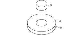
- FIG. 3 is a perspective view showing the heat transfer member 30, and FIG. 4 is an exploded perspective view showing the heat transfer member 30. More specifically, as shown in FIGS. 1 to 4, the heat transfer member 30 includes a first heat transfer unit 32 and a second heat transfer unit 36.
- the first heat transfer portion 32 is a portion of the heat transfer member 30 on which the one end surface is formed.
- the second heat transfer portion 36 is a portion joined to the first heat transfer portion 32 on the side opposite to the one end surface.
- the first heat transfer portion 32 is formed in a shape that can be arranged while being contained in the through hole 21h.
- the first heat transfer portion 32 is formed in a columnar shape.
- the height of the first heat transfer portion 32 is formed to be the same as the thickness of the substrate 20.
- the diameter of the first heat transfer portion 32 is formed to be the same as or smaller (slightly smaller) than the diameter of the through hole 21h.
- the second heat transfer portion 36 is arranged in the through hole 21h in a state where one end surface thereof is flush with one main surface of the substrate 20.
- the first heat transfer portion 32 may be formed of copper or a copper alloy. As a result, the first heat transfer portion 32 is satisfactorily soldered to the heat generating component 40.
- first heat transfer portion 32 may be satisfactorily soldered to the conductive layer 25 in the through hole 21h. Further, the first heat transfer portion 32 formed of copper or a copper alloy has good thermal conductivity. The dimensions of the first heat transfer portion 32 may be set so as to be press-fitted into the through hole 21h, or may be set so as to be inserted at a distance from the through hole 21h. May be good.
- the second heat transfer portion 36 is preferably formed of aluminum or an aluminum alloy. Further, it is preferable that the alumite film 37 is formed on at least a part of the surface of the second heat transfer portion 36.
- the thermal conductivity of aluminum or aluminum alloy is inferior to that of copper or copper alloy, but better than other common insulating materials such as resins. Therefore, the second heat transfer portion 36 made of aluminum or an aluminum alloy also has good thermal conductivity. Further, the alumite film 37 exhibits insulating properties. Therefore, at least a part of the surface of the second heat transfer portion 36 can be provided with insulating properties.
- the alumite film 37 is preferably formed on at least the other end surface (the surface facing the heat radiating member 60) of the second heat transfer portion 36.
- the alumite film 37 may also be formed on the peripheral surface of the second heat transfer portion 36.
- the configuration for joining the first heat transfer unit 32 and the second heat transfer unit 36 is not particularly limited.
- the first heat transfer portion 32 and the second heat transfer portion 36 may be joined by a joining method between dissimilar metals, for example, a diffusion joining method or a rolling joining method.
- a clad material obtained by diffusion-bonding a flat copper plate material and an aluminum plate material may be processed into the shape of the heat transfer member 30 by grinding.
- the other end of the heat transfer member 30 projects from the other main surface of the substrate 20.
- the second heat transfer portion 36 is formed in a plate shape protruding around the first heat transfer portion 32.
- the second heat transfer portion 36 projects from the other main surface of the substrate 20.
- the second heat transfer portion 36 is formed in a disk shape. With the first heat transfer portion 32 inserted into the through hole 21h, the second heat transfer portion 36 can come into contact with the other main surface of the substrate 20 around the through hole 21h. As a result, the heat transfer member 30 is positioned in the thickness direction of the substrate 20.
- the second heat transfer portion 36 may have an elliptical plate shape or a polygonal plate shape. The second heat transfer section does not need to extend around the first heat transfer section.
- thermosetting adhesive 28 is adhered to the other main surface of the substrate 20 by the thermosetting adhesive 28. May be.
- the thermosetting adhesive 28 is cured by heat and does not soften even when reheated. Therefore, if the second heat transfer portion 36 is adhered to the substrate 20 with the heat-curable adhesive 28, even if the heat transfer member 30 and the substrate 20 are heated during soldering, the heat transfer member 30 will be attached to the substrate. It is hard to drop out from 20.
- the substrate 20 also has a component 48 other than the heat generating component 40 mounted on the substrate 20.
- the component 48 is a terminal, a connector, or the like for connecting the wiring of the substrate 20 to another.
- the heat radiating member 60 is arranged on the other main surface side of the substrate 20.
- the heat radiating member 60 is made of a material having good thermal conductivity, such as copper, a copper alloy, aluminum, and an aluminum alloy.
- the heat radiating member 60 includes a plate portion 62 and a heat radiating structure portion 64.
- the plate portion 62 has a flat surface, and the flat surface is arranged so as to face the other main surface of the substrate 20.
- the heat radiating structure portion 64 has a shape for increasing the surface area, for example, a fin structure. The heat transferred to the heat radiating member 60 is released to the outside from the heat radiating structure portion 64.
- an insulating spacer 68 is interposed between one main surface of the heat radiating member 60 and the other main surface of the substrate 20.
- the insulating spacer 68 may be provided over the entire one main surface of the heat radiating member 60, or may be partially provided, except for the portion where the heat transfer member 30 is provided.
- the insulating spacer 68 is provided at four corners of one main surface of the heat radiating member 60.
- a recess 63 in which the second heat transfer portion 36 is housed is formed on one main surface of the heat radiating member 60, the other end of the heat transfer member 30, here.
- the recess 63 is formed in the shape of a bottomed circular hole.
- the diameter of the recess 63 is the same as or larger (slightly larger) than the diameter of the second heat transfer portion 36.
- the second heat transfer portion 36 projects from the other main surface of the substrate 20 and is partially housed in the recess 63.
- a heat conductive material 69 is provided on the bottom side in the recess 63.
- the thermally conductive material 69 is a material also called a thermal interface material (TIM).
- the heat conductive material 69 is, for example, a heat conductive sheet using a silicone resin, a heat conductive grease, or the like.
- the heat conductive material 69 is interposed between the other main surface of the heat transfer member 30 (the outward end surface of the second heat transfer portion 36) and the bottom surface of the recess 63.
- the heat transferred to the second heat transfer unit 36 can be transferred to the heat radiating member 60 via the heat conductive material 69.
- the heat transfer member 30 is prepared (see step (a), FIGS. 3 and 4).
- the nickel base plating layer 33 is formed on at least one end surface of the heat transfer member 30 in the state before soldering. Further, a gold plating layer 34 is formed on the surface of the nickel base plating layer 33.
- the first heat transfer portion 32 of the heat transfer member 30 is formed of pure copper (alloy number C1020) or the like.
- the size of the first heat transfer unit 32 is adjusted to the size of the heat generating component 40 mounted on the substrate 20.
- the heat generating component 40 is a MOSFET (metal-oxide-semiconductor field-effect transistor) corresponding to the package TO-263, which is one of the standard products of JEDEC (Joint Electron Device Engineering Council standards).
- the dimensions of the drain electrode of the heat generating component 40 are approximately 6 mm in length and 6 mm in width, so that the outer diameter of the first heat transfer portion 32 may be set to 6 mm.
- the size of the heat generating component 40 is adjusted, it is difficult to increase the size of the first heat transfer portion 32 of the heat transfer member 30, and the thermal resistance increases.
- the axial length of the first heat transfer portion 32 is such that one end surface of the heat transfer member 30 is aligned with the conductive layer (also called a land) 23 of the substrate 20 in a state of being soldered to the substrate 20.
- the thickness is the same as that of the substrate 20.
- the axial length of the first heat transfer portion 32 is 2 mm.
- the surface of the first heat transfer unit 32 is treated with the surface of the second heat transfer unit 36 masked.
- surface treatment is performed on the entire surface of the first heat transfer portion 32, excluding the portion joined to the second heat transfer portion 36, that is, one end surface and the peripheral surface of the first heat transfer portion 32.
- the first heat transfer portion 32 is subjected to an electroless nickel base flash gold plating treatment.
- the thickness of the nickel base plating layer 33 formed by the electroless nickel base gold plating treatment is, for example, 1 ⁇ m or more and 3 ⁇ m or less, and the thickness of the gold plating layer 34 is, for example, 0.01 ⁇ m or more and 0.03 ⁇ m or less.
- the second heat transfer portion 36 is made of aluminum (alloy number A1050) or the like.
- the outer diameter of the second heat transfer unit 36 is preferably set to a size that does not interfere with the heat radiation member 60 or the like in a state where the heat transfer member 30 is soldered to the substrate 20.
- the outer diameter of the second heat transfer unit 36 is set to 20 mm.
- the thickness of the second heat transfer portion 36 may be set as large as possible so that the heat capacity can be increased. However, if the heat capacity of the second heat transfer unit 36 becomes too large, it is necessary to set the reflow set temperature at the time of soldering high, which may cause the reflow set temperature to exceed the heat resistant temperature of other mounted components.
- the thickness of the second heat transfer portion 36 is preferably set within a range in consideration of them, and is preferably set to, for example, 20 mm.
- the surface of the second heat transfer portion 36 is subjected to an alumite processing treatment such as anodizing treatment.
- an alumite processing treatment such as anodizing treatment.
- the alumite film 37 is formed on the other main surface and the peripheral surface of the second heat transfer portion 36.
- the thickness of the alumite film 37 is, for example, 20 ⁇ m or more and 70 ⁇ m or less.
- a substrate 20 as shown in FIG. 5 is prepared.
- a through hole 21h is formed in the substrate 20.
- the conductive layers 23 and 25 are formed on the substrate 20.
- the outer diameter of the through hole 21h is set to a size that allows the first heat transfer portion 32 of the heat transfer member 30 to be mounted.
- the surfaces of the conductive layers 23 and 25 may be subjected to electroless nickel base flash gold plating treatment in the same manner as the surface of the first heat transfer portion 32.
- the thickness of the nickel base plating layer is preferably set to 1 ⁇ m or more and 3 ⁇ m or less.
- the thickness of the gold plating layer may be set to 0.01 ⁇ m or more and 0.03 ⁇ m or less.
- a power supply circuit and a signal circuit are formed on the substrate 20 by the conductive layer 23.
- the board 20 is formed with through holes for mounting components 48 such as power supply terminals and signal terminals for connecting the power supply circuit and the signal circuit to the external circuit.
- the heat transfer member 30 is inserted into the through hole 21h in the substrate 20 (step (b)).
- the heat transfer member 30 is inserted from the other main surface side of the substrate 20.
- eight through holes 21h are formed, and the heat transfer member 30 is inserted into each through hole 21h.
- thermosetting adhesive 28 for example, a thermosetting epoxy adhesive is used.
- the coating region of the thermosetting adhesive 28 is the contact region between the substrate 20 and the second heat transfer portion 36, that is, the portion of the other main surface of the substrate 20 around the through hole 21h and the second heat transfer portion 36. It is a contact portion with the surface of the substrate 20. It is preferable that the thermosetting adhesive 28 does not flow between the first heat transfer portion 32 and the through hole 21h.
- the heat generating component 40 is soldered to one end surface of the heat transfer member 30 (step (C)). More specifically, on one main surface of the substrate 20, one end surface of the heat generating component 40 is exposed and a part (land) of the conductive layer 23 around it is integrally spread, and heat is generated on these surfaces.
- the terminals of the component 40 (here, the drain terminals of the MOSFET) are soldered.
- the other terminals of the heat generating component 40 (here, the source terminal of the MOSFET and the gate terminal) are soldered to the other portion (land) of the conductive layer 23 on one main surface of the substrate 20. Soldering is performed by, for example, reflow soldering.
- the surface of the first heat transfer portion 32 is subjected to a nickel base metal flash plating treatment. That is, the nickel base plating layer 33 is formed on the surface of the first heat transfer portion 32. A gold plating layer 34 is formed on the surface of the nickel base plating layer 33.
- the solder paste 50a is applied to the surface of the gold plating layer 34, and the heat generating component 40 is placed on the solder paste 50a and heated.
- the solder is soldered to the nickel base plating layer 33 in a state where the gold plating layer 34 on the outermost surface is dissolved in the solder. ..
- the melted solder can be well adapted to the surface of the first heat transfer portion 32, and metal oxides, which are factors for generating voids, are less likely to be generated, so that the first heat transfer portion 32 and the heat generating component 40 are less likely to be generated. Voids are unlikely to occur between and. Similarly, if the surfaces of the conductive layers 23 and 25 are also subjected to nickel base metal flash plating, voids are unlikely to occur. As a result of making it difficult for voids, which are an air layer, to be generated in the solder portion 50 between the heat transfer member 30 and the heat generating component 40, an increase and variation in thermal resistance between the heat transfer member 30 and the heat generating component 40 are suppressed. Be done.
- the solder wettability on the surface of the heat transfer member 30 is improved, the melted solder easily flows into the gap between the first heat transfer portion 32 and the through hole 21h, and the melted solder easily flows into the gap between the first heat transfer portion 32 and the through hole 21h. A strong joint state can be obtained with. Therefore, the connection reliability between the heat transfer member 30 and the substrate 20 is improved. For example, the occurrence of cracks due to the thermal cycle test is reduced.
- parts 48 such as power supply terminals and signal terminals are soldered to the substrate 20.
- the heat radiating member 60 is assembled on the other main surface side of the substrate 20.
- the heat radiating member 60 and the substrate 20 may be fixed by screwing or by an adhesive.
- the heat radiating member 60 is formed with the recess 63.
- the heat conductive material 69 is arranged in the recess 63.
- the heat conductive material 69 for example, a heat conductive silicone grease having a thermal conductivity of 2 W / m ⁇ K or more and a viscosity of 50 Pa ⁇ s or more and 500 Pa ⁇ s or less is used.
- the thermally conductive silicone grease is applied so as to cover the entire bottom surface of the recess 63. After that, the other main surface of the second heat transfer portion 36 is pushed toward the back of the recess 63, and the thickness of the heat conductive material 69 is controlled to be 0.5 mm or more and 1.0 mm or less.
- the interposition state of the heat conductive material 69 is stable between the second heat transfer portion 36 and the heat radiating member 60.
- the heat conductive material 69 is a fluid
- the fluid is stably contained in the recess 63, so that the heat conductive material 69 is unlikely to spread widely around.
- the heat generated by the heat radiation member 60 is transferred to the heat radiation member 60 via the first heat transfer unit 32, the second heat transfer unit 36, and the heat conductive material 69. ..
- the heat is mainly released to the outside in the heat radiating member 60.
- thermal resistance is expressed by the following equation.
- Thermal resistance (° C / W) thickness (m) ⁇ ⁇ cross-sectional area (m 2 ) x thermal conductivity (W / mK) ⁇ Therefore, it can be seen that the thermal resistance decreases as the cross-sectional area (the contact area) increases, and the thermal resistance decreases as the thermal conductivity increases.
- the thermal conductivity is 398 W / mK.
- the thermal conductivity of the alumite film 37 in the second heat transfer section 36 drops to 80 W / mK, which is equivalent to about 1/3 of that in the untreated state. If the material of the second heat transfer portion 36 is copper, it is necessary to coat the surface with a resin by electrodeposition coating or the like as an insulating treatment. In that case, the thermal conductivity drops significantly to about 0.4 W / mK.
- the thermal conductivity can be increased while ensuring the insulating property. It can be seen from the above equation that the thermal resistance can be suppressed to a small value as the thermal conductivity increases.
- the outer diameter of the second heat transfer portion 36 is increased with respect to the outer diameter of the first heat transfer portion 32, for example, the outer diameter of the second heat transfer portion 36 is 6 mm with respect to the outer diameter of the first heat transfer portion 32.
- the nickel base plating layer 33 is formed on one end surface of the heat transfer member 30.
- the nickel base plating layer 33 can be kept in a state in which oxidation is suppressed by the gold plating layer 34.
- the gold plating layer 34 is mixed with the molten solder, and the solder portion 50 is soldered to the nickel base plating layer 33.
- the molten solder blends well with the gold-plated nickel base plating layer 33, and is well soldered to the nickel base plating layer 33 with suppressed oxidation. As a result, voids are less likely to occur on the surface of the heat transfer member 30. As a result, the increase and variation in thermal resistance are suppressed.
- the molten solder easily flows into the gap between the heat transfer member 30 and the through hole 21h, so that the heat transfer member The bond between 30 and the substrate 20 becomes stronger.
- the heat transfer member 40 heats well to the heat transfer member 30. Can be transmitted. Since the portion of the heat transfer member 30 opposite to the side on which the heat generating component 40 is mounted is also the second heat transfer portion 36 formed of aluminum or an aluminum alloy, the heat transferred to the heat transfer member 30 is opposite. It can be transmitted well toward the main surface of the side.
- An alumite film 37 is formed on at least a part of the surface of the second heat transfer portion 36, and the alumite film 37 has an insulating property.
- the heat transfer member 30 and the heat radiating member 60 have an insulating property. Easy to secure. Therefore, while ensuring the insulating property between the heat transfer member 30 and the heat radiating member 60. Heat is easily transferred from the heat transfer member 30 to the heat dissipation member 60.
- the alumite film 37 ensures the insulating property between the heat transfer member 30 and the heat radiation member 60. ..
- the second heat transfer portion 36 is formed in a plate shape protruding around the first heat transfer portion 32. Therefore, the surface area of the other main surface of the second heat transfer portion 36 becomes large. As a result, the contact area between the heat transfer member 30 and the heat radiating member 60 becomes large, and heat is effectively released from the heat transfer member 30 through the heat radiating member 60 and the like.
- thermosetting adhesive 28 since the heat transfer member 30 and the substrate 20 are adhered to each other by the thermosetting adhesive 28, the heat transfer member 30 is unlikely to fall off from the substrate during soldering.
- a recess 63 is formed in the heat radiating member 60, and a heat conductive material 69 is interposed between the bottom of the recess 63 and the other end of the heat transfer member 30. Therefore, the interposition state of the heat conductive material 69 is stabilized between the heat transfer member 30 and the heat radiation member 60. As a result, the heat dissipation performance is stabilized via the heat dissipation member 60.
- the heat conductive material 69 is a fluid such as heat conductive grease
- the distance between the heat transfer member 30 and the heat radiation member 60 changes due to heat expansion and contraction of the heat transfer member 30 and the substrate 20. There is a fear. If this interval changes, the way the thermally conductive grease or the like spreads may fluctuate.
- a fluid such as heat conductive grease is filled in the recess 63, even if the heat transfer member 30 and the substrate 20 undergo thermal expansion and contraction, they are likely to be kept in the recess 63. Therefore, the thermal conductivity from the heat transfer member 30 to the heat dissipation member 60 is stable.
- the void 100 was hardly generated, and even if it was generated, only a small void was generated.
- Substrate with heat transfer member 20 Substrate 21h Through hole 22 Insulation plate 23 Conductive layer 25 Conductive layer 28 Heat-curable adhesive 30 Heat transfer member 32 1st heat transfer part 33 Nickel base plating layer 34 Gold plating layer 36 2nd heat transfer Part 37 Alumite film 40 Heat-generating parts 48 Parts 50 Solder part 50a Solder paste 60 Heat-dissipating member 62 Plate part 63 Recessed 64 Heat-dissipating structure part 68 Insulation spacer 69 Thermal conductive material 100 Void 130 Heat transfer member
Landscapes
- Engineering & Computer Science (AREA)
- Microelectronics & Electronic Packaging (AREA)
- Manufacturing & Machinery (AREA)
- Physics & Mathematics (AREA)
- Thermal Sciences (AREA)
- Cooling Or The Like Of Semiconductors Or Solid State Devices (AREA)
- Cooling Or The Like Of Electrical Apparatus (AREA)
- Structure Of Printed Boards (AREA)
Priority Applications (2)
| Application Number | Priority Date | Filing Date | Title |
|---|---|---|---|
| CN202080073206.0A CN114631400B (zh) | 2019-10-28 | 2020-09-02 | 带传热构件的基板以及带传热构件的基板的制造方法 |
| US17/755,391 US20220408545A1 (en) | 2019-10-28 | 2020-09-02 | Heat transfer member-equipped substrate and method for manufacturing heat transfer member-equipped substate |
Applications Claiming Priority (2)
| Application Number | Priority Date | Filing Date | Title |
|---|---|---|---|
| JP2019-195337 | 2019-10-28 | ||
| JP2019195337A JP7251446B2 (ja) | 2019-10-28 | 2019-10-28 | 伝熱部材付基板及び伝熱部材付基板の製造方法 |
Publications (1)
| Publication Number | Publication Date |
|---|---|
| WO2021084897A1 true WO2021084897A1 (ja) | 2021-05-06 |
Family
ID=75638614
Family Applications (1)
| Application Number | Title | Priority Date | Filing Date |
|---|---|---|---|
| PCT/JP2020/033256 Ceased WO2021084897A1 (ja) | 2019-10-28 | 2020-09-02 | 伝熱部材付基板及び伝熱部材付基板の製造方法 |
Country Status (4)
| Country | Link |
|---|---|
| US (1) | US20220408545A1 (https=) |
| JP (1) | JP7251446B2 (https=) |
| CN (1) | CN114631400B (https=) |
| WO (1) | WO2021084897A1 (https=) |
Families Citing this family (3)
| Publication number | Priority date | Publication date | Assignee | Title |
|---|---|---|---|---|
| US12171056B2 (en) * | 2022-06-20 | 2024-12-17 | Mellanox Technologies Ltd. | Electronic assembly and method for thermal balancing of surfacemount devices |
| CN117177473B (zh) * | 2023-10-18 | 2024-08-30 | 芜湖雅葆轩电子科技股份有限公司 | 一种元件贴装前的罩式分区定点融锡装置 |
| TWI860876B (zh) * | 2023-10-23 | 2024-11-01 | 啓碁科技股份有限公司 | 散熱結構 |
Citations (3)
| Publication number | Priority date | Publication date | Assignee | Title |
|---|---|---|---|---|
| JP2011159702A (ja) * | 2010-01-29 | 2011-08-18 | Denso Corp | 半導体装置およびその製造方法 |
| JP2012099540A (ja) * | 2010-10-29 | 2012-05-24 | Shinko Electric Ind Co Ltd | 配線基板及びその製造方法、電子装置 |
| JP2014135418A (ja) * | 2013-01-11 | 2014-07-24 | Hitachi Automotive Systems Ltd | 車載用電子制御装置 |
Family Cites Families (22)
| Publication number | Priority date | Publication date | Assignee | Title |
|---|---|---|---|---|
| JPH04192552A (ja) * | 1990-11-27 | 1992-07-10 | Nec Corp | 半導体素子用パッケージ |
| JPH05259321A (ja) * | 1992-03-11 | 1993-10-08 | Toshiba Corp | マルチチップモジュール |
| US20020045036A1 (en) * | 1999-06-16 | 2002-04-18 | Robin Gorrell | Bga solder ball shear strength |
| JP2003023250A (ja) * | 2001-07-06 | 2003-01-24 | Denso Corp | 多層基板のおよびその製造方法 |
| JP2003198117A (ja) * | 2001-12-28 | 2003-07-11 | Matsushita Electric Ind Co Ltd | はんだ付け方法および接合構造体 |
| JP2004172313A (ja) * | 2002-11-19 | 2004-06-17 | Nitto Denko Corp | 熱伝導性放熱シートおよびこれを用いた半導体装置 |
| JP2006165114A (ja) * | 2004-12-03 | 2006-06-22 | Nec Corp | 半導体素子の実装方法及び実装構造、装置 |
| US7807560B2 (en) * | 2007-07-17 | 2010-10-05 | Shinko Electric Industries Co., Ltd. | Solder bump forming method |
| JP2012033855A (ja) * | 2010-07-01 | 2012-02-16 | Hitachi Cable Ltd | Ledモジュール、ledパッケージ、並びに配線基板およびその製造方法 |
| CN202026521U (zh) * | 2011-02-28 | 2011-11-02 | 张�林 | 带散热金属的电路板 |
| JP6061369B2 (ja) * | 2012-01-30 | 2017-01-18 | 凸版印刷株式会社 | 配線基板およびその製造方法、ならびにはんだ付き配線基板の製造方法 |
| JP5989465B2 (ja) * | 2012-09-05 | 2016-09-07 | 昭和電工株式会社 | 絶縁基板の製造方法 |
| JP6197619B2 (ja) * | 2013-12-09 | 2017-09-20 | 富士通株式会社 | 電子装置及び電子装置の製造方法 |
| JP6213291B2 (ja) | 2014-02-17 | 2017-10-18 | 三菱マテリアル株式会社 | ヒートシンク付パワーモジュール用基板の製造方法 |
| JP2015177157A (ja) * | 2014-03-18 | 2015-10-05 | 三菱電機株式会社 | 電子機器 |
| JP6547134B2 (ja) * | 2014-05-22 | 2019-07-24 | パナソニックIpマネジメント株式会社 | 回路基板 |
| JP6333215B2 (ja) * | 2015-05-19 | 2018-05-30 | オムロンオートモーティブエレクトロニクス株式会社 | プリント基板、電子装置 |
| AT518281B1 (de) * | 2016-03-01 | 2017-09-15 | Zkw Group Gmbh | Verfahren zum Herstellen einer Schirmung |
| EP3428223B1 (en) * | 2016-03-10 | 2021-05-05 | Denka Company Limited | Ceramic resin composite body |
| US11133445B2 (en) * | 2017-03-22 | 2021-09-28 | Denka Company Limited | Resin composition for circuit board, and metal-base circuit board in which same is used |
| DE112018006380T5 (de) * | 2017-12-14 | 2020-08-27 | Autonetworks Technologies, Ltd. | Schaltungsanordnung und elektrischer Verteilerkasten |
| JP2019176015A (ja) | 2018-03-28 | 2019-10-10 | 株式会社Uacj | 回路基板付きヒートシンク及びその製造方法 |
-
2019
- 2019-10-28 JP JP2019195337A patent/JP7251446B2/ja active Active
-
2020
- 2020-09-02 CN CN202080073206.0A patent/CN114631400B/zh active Active
- 2020-09-02 WO PCT/JP2020/033256 patent/WO2021084897A1/ja not_active Ceased
- 2020-09-02 US US17/755,391 patent/US20220408545A1/en not_active Abandoned
Patent Citations (3)
| Publication number | Priority date | Publication date | Assignee | Title |
|---|---|---|---|---|
| JP2011159702A (ja) * | 2010-01-29 | 2011-08-18 | Denso Corp | 半導体装置およびその製造方法 |
| JP2012099540A (ja) * | 2010-10-29 | 2012-05-24 | Shinko Electric Ind Co Ltd | 配線基板及びその製造方法、電子装置 |
| JP2014135418A (ja) * | 2013-01-11 | 2014-07-24 | Hitachi Automotive Systems Ltd | 車載用電子制御装置 |
Also Published As
| Publication number | Publication date |
|---|---|
| JP2021068868A (ja) | 2021-04-30 |
| JP7251446B2 (ja) | 2023-04-04 |
| US20220408545A1 (en) | 2022-12-22 |
| CN114631400A (zh) | 2022-06-14 |
| CN114631400B (zh) | 2024-03-26 |
Similar Documents
| Publication | Publication Date | Title |
|---|---|---|
| JP7023298B2 (ja) | 電力変換装置及び電力変換装置の製造方法 | |
| JP4159861B2 (ja) | プリント回路基板の放熱構造の製造方法 | |
| US10978371B2 (en) | Semiconductor device and method for manufacturing semiconductor device | |
| JP2009044156A (ja) | 改善された放熱性を備えた回路支持体構造部 | |
| JP5071405B2 (ja) | 電力用半導体装置 | |
| CN110506455A (zh) | 附带金属构件的基板、电路结构体及电气连接箱 | |
| WO2012108011A1 (ja) | パワー半導体モジュール | |
| JP7251446B2 (ja) | 伝熱部材付基板及び伝熱部材付基板の製造方法 | |
| US6657866B2 (en) | Electronics assembly with improved heatsink configuration | |
| US11295997B2 (en) | Semiconductor device manufacturing method and semiconductor device | |
| US20160021788A1 (en) | Electronic device assembly | |
| WO2018193828A1 (ja) | 金属部材付き基板、回路構成体及び電気接続箱 | |
| JPWO2022044541A5 (https=) | ||
| JP2008277330A (ja) | 放熱装置 | |
| US12548705B2 (en) | Integrated voltage regulator | |
| WO2020195103A1 (ja) | 回路基板及び、回路基板を含む電気接続箱の製造方法 | |
| JP6984257B2 (ja) | 電子装置 | |
| JP2013183038A (ja) | 半導体装置 | |
| JP6011410B2 (ja) | 半導体装置用接合体、パワーモジュール用基板及びパワーモジュール | |
| CN111052510B (zh) | 半导体装置 | |
| CN114450784A (zh) | 功率半导体构件以及用于制造功率半导体构件的方法 | |
| WO2022004332A1 (ja) | 回路構成体 | |
| JP6403741B2 (ja) | 表面実装型半導体パッケージ装置 | |
| JP2002076259A (ja) | パワーモジュール | |
| JP2009141236A (ja) | 電子回路の実装方法及び実装構造 |
Legal Events
| Date | Code | Title | Description |
|---|---|---|---|
| 121 | Ep: the epo has been informed by wipo that ep was designated in this application |
Ref document number: 20880361 Country of ref document: EP Kind code of ref document: A1 |
|
| NENP | Non-entry into the national phase |
Ref country code: DE |
|
| 122 | Ep: pct application non-entry in european phase |
Ref document number: 20880361 Country of ref document: EP Kind code of ref document: A1 |