WO2021010063A1 - シャフト付きセラミックヒータ - Google Patents
シャフト付きセラミックヒータ Download PDFInfo
- Publication number
- WO2021010063A1 WO2021010063A1 PCT/JP2020/022835 JP2020022835W WO2021010063A1 WO 2021010063 A1 WO2021010063 A1 WO 2021010063A1 JP 2020022835 W JP2020022835 W JP 2020022835W WO 2021010063 A1 WO2021010063 A1 WO 2021010063A1
- Authority
- WO
- WIPO (PCT)
- Prior art keywords
- ceramic
- shaft
- resistance heating
- heating element
- ceramic heater
- Prior art date
- Legal status (The legal status is an assumption and is not a legal conclusion. Google has not performed a legal analysis and makes no representation as to the accuracy of the status listed.)
- Ceased
Links
Images



Classifications
-
- H—ELECTRICITY
- H05—ELECTRIC TECHNIQUES NOT OTHERWISE PROVIDED FOR
- H05B—ELECTRIC HEATING; ELECTRIC LIGHT SOURCES NOT OTHERWISE PROVIDED FOR; CIRCUIT ARRANGEMENTS FOR ELECTRIC LIGHT SOURCES, IN GENERAL
- H05B3/00—Ohmic-resistance heating
- H05B3/10—Heating elements characterised by the composition or nature of the materials or by the arrangement of the conductor
- H05B3/12—Heating elements characterised by the composition or nature of the materials or by the arrangement of the conductor characterised by the composition or nature of the conductive material
- H05B3/14—Heating elements characterised by the composition or nature of the materials or by the arrangement of the conductor characterised by the composition or nature of the conductive material the material being non-metallic
- H05B3/141—Conductive ceramics, e.g. metal oxides, metal carbides, barium titanate, ferrites, zirconia, vitrous compounds
- H05B3/143—Conductive ceramics, e.g. metal oxides, metal carbides, barium titanate, ferrites, zirconia, vitrous compounds applied to semiconductors, e.g. wafers heating
-
- H—ELECTRICITY
- H05—ELECTRIC TECHNIQUES NOT OTHERWISE PROVIDED FOR
- H05B—ELECTRIC HEATING; ELECTRIC LIGHT SOURCES NOT OTHERWISE PROVIDED FOR; CIRCUIT ARRANGEMENTS FOR ELECTRIC LIGHT SOURCES, IN GENERAL
- H05B3/00—Ohmic-resistance heating
- H05B3/02—Details
-
- H—ELECTRICITY
- H10—SEMICONDUCTOR DEVICES; ELECTRIC SOLID-STATE DEVICES NOT OTHERWISE PROVIDED FOR
- H10P—GENERIC PROCESSES OR APPARATUS FOR THE MANUFACTURE OR TREATMENT OF DEVICES COVERED BY CLASS H10
- H10P72/00—Handling or holding of wafers, substrates or devices during manufacture or treatment thereof
- H10P72/04—Apparatus for manufacture or treatment
- H10P72/0431—Apparatus for thermal treatment
- H10P72/0432—Apparatus for thermal treatment mainly by conduction
-
- H—ELECTRICITY
- H05—ELECTRIC TECHNIQUES NOT OTHERWISE PROVIDED FOR
- H05B—ELECTRIC HEATING; ELECTRIC LIGHT SOURCES NOT OTHERWISE PROVIDED FOR; CIRCUIT ARRANGEMENTS FOR ELECTRIC LIGHT SOURCES, IN GENERAL
- H05B3/00—Ohmic-resistance heating
- H05B3/20—Heating elements having extended surface area substantially in a two-dimensional [2D] plane, e.g. plate-heater
- H05B3/22—Heating elements having extended surface area substantially in a two-dimensional [2D] plane, e.g. plate-heater non-flexible
- H05B3/28—Heating elements having extended surface area substantially in a two-dimensional [2D] plane, e.g. plate-heater non-flexible heating conductor embedded in insulating material
- H05B3/283—Heating elements having extended surface area substantially in a two-dimensional [2D] plane, e.g. plate-heater non-flexible heating conductor embedded in insulating material the insulating material being an inorganic material, e.g. ceramic
-
- H—ELECTRICITY
- H05—ELECTRIC TECHNIQUES NOT OTHERWISE PROVIDED FOR
- H05B—ELECTRIC HEATING; ELECTRIC LIGHT SOURCES NOT OTHERWISE PROVIDED FOR; CIRCUIT ARRANGEMENTS FOR ELECTRIC LIGHT SOURCES, IN GENERAL
- H05B3/00—Ohmic-resistance heating
- H05B3/68—Heating arrangements specially adapted for cooking plates or analogous hot-plates
- H05B3/74—Non-metallic plates, e.g. vitroceramic, ceramic or glassceramic hobs, also including power or control circuits
-
- H—ELECTRICITY
- H10—SEMICONDUCTOR DEVICES; ELECTRIC SOLID-STATE DEVICES NOT OTHERWISE PROVIDED FOR
- H10P—GENERIC PROCESSES OR APPARATUS FOR THE MANUFACTURE OR TREATMENT OF DEVICES COVERED BY CLASS H10
- H10P72/00—Handling or holding of wafers, substrates or devices during manufacture or treatment thereof
- H10P72/70—Handling or holding of wafers, substrates or devices during manufacture or treatment thereof for supporting or gripping
-
- H—ELECTRICITY
- H10—SEMICONDUCTOR DEVICES; ELECTRIC SOLID-STATE DEVICES NOT OTHERWISE PROVIDED FOR
- H10P—GENERIC PROCESSES OR APPARATUS FOR THE MANUFACTURE OR TREATMENT OF DEVICES COVERED BY CLASS H10
- H10P72/00—Handling or holding of wafers, substrates or devices during manufacture or treatment thereof
- H10P72/70—Handling or holding of wafers, substrates or devices during manufacture or treatment thereof for supporting or gripping
- H10P72/76—Handling or holding of wafers, substrates or devices during manufacture or treatment thereof for supporting or gripping using mechanical means, e.g. clamps or pinches
- H10P72/7604—Handling or holding of wafers, substrates or devices during manufacture or treatment thereof for supporting or gripping using mechanical means, e.g. clamps or pinches the wafers being placed on a susceptor, stage or support
- H10P72/7626—Handling or holding of wafers, substrates or devices during manufacture or treatment thereof for supporting or gripping using mechanical means, e.g. clamps or pinches the wafers being placed on a susceptor, stage or support characterised by the construction of the shaft
-
- H—ELECTRICITY
- H10—SEMICONDUCTOR DEVICES; ELECTRIC SOLID-STATE DEVICES NOT OTHERWISE PROVIDED FOR
- H10P—GENERIC PROCESSES OR APPARATUS FOR THE MANUFACTURE OR TREATMENT OF DEVICES COVERED BY CLASS H10
- H10P95/00—Generic processes or apparatus for manufacture or treatments not covered by the other groups of this subclass
-
- H—ELECTRICITY
- H05—ELECTRIC TECHNIQUES NOT OTHERWISE PROVIDED FOR
- H05B—ELECTRIC HEATING; ELECTRIC LIGHT SOURCES NOT OTHERWISE PROVIDED FOR; CIRCUIT ARRANGEMENTS FOR ELECTRIC LIGHT SOURCES, IN GENERAL
- H05B2203/00—Aspects relating to Ohmic resistive heating covered by group H05B3/00
- H05B2203/016—Heaters using particular connecting means
-
- H—ELECTRICITY
- H05—ELECTRIC TECHNIQUES NOT OTHERWISE PROVIDED FOR
- H05B—ELECTRIC HEATING; ELECTRIC LIGHT SOURCES NOT OTHERWISE PROVIDED FOR; CIRCUIT ARRANGEMENTS FOR ELECTRIC LIGHT SOURCES, IN GENERAL
- H05B2203/00—Aspects relating to Ohmic resistive heating covered by group H05B3/00
- H05B2203/017—Manufacturing methods or apparatus for heaters
Definitions
- the present invention relates to a ceramic heater with a shaft.
- a ceramic heater with a shaft for holding a wafer is used in a film forming process such as transporting, exposing, and CVD of a semiconductor wafer, and in microfabrication such as cleaning, etching, and dicing.
- a ceramic heater with a shaft as shown in Patent Document 1, a ceramic plate in which a resistance heating element is embedded, a hollow ceramic shaft joined to a surface of the ceramic plate opposite to the wafer mounting surface, and a ceramic A conductive film formed so as to extend the inner peripheral wall surface of the shaft in the vertical direction and a wire for electrically connecting the resistance heating element and the conductive film are disclosed (see FIG. 5). ..
- the present invention has been made to solve such a problem, and its main object is to make it difficult to connect adjacent conductive films.
- the ceramic heater with a shaft of the present invention A ceramic plate with an embedded resistance heating element and A hollow ceramic shaft joined to the surface of the ceramic plate opposite to the wafer mounting surface, A plurality of vertical grooves provided along the axial direction on the inner peripheral surface of the ceramic shaft, and The conductive film formed in the plurality of flutes and A connecting member that electrically connects the terminal of the resistance heating element and the conductive film, It is equipped with.
- the conductive film is formed in a vertical groove provided along the axial direction on the inner peripheral surface of the ceramic shaft. Therefore, the adjacent conductive films are separated by a boundary portion between the flutes and the flutes in the ceramic shaft. Therefore, adjacent conductive films are difficult to connect due to the presence of such a boundary portion.
- the resistance heating element is provided in each of a plurality of zones of the ceramic plate, and two terminals are independently provided for each resistance heating element.
- Two conductive films may be provided independently for each resistance heating element.
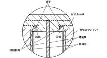
- the conductive film and the connecting member may be covered with an insulating film.
- an insulating film is preferably an aerosol deposition (AD) film or a thermal sprayed film.
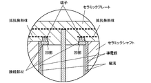
- FIG. 1 is a vertical cross-sectional view of the ceramic heater with a shaft of the present embodiment.
- the ceramic heater with a shaft includes a ceramic plate, a ceramic shaft, a vertical groove, a conductive film, a recess (see FIG. 2), and a connecting member.
- An RF electrode and a resistance heating element are embedded in the ceramic plate.
- the RF electrode is an electrode to which a high frequency voltage is applied when generating plasma.
- the RF feeding rod is housed in the internal space of the ceramic shaft, and is joined to the RF electrode from the surface of the ceramic plate opposite to the wafer mounting surface.
- the resistance heating element heats the ceramic plate when energized.
- the resistance heating elements are provided in each of the plurality (three) zones of the ceramic plate. Two terminals are provided independently for each resistance heating element.
- the ceramic shaft is a hollow shaft bonded to the surface of the ceramic plate opposite to the wafer mounting surface by direct bonding.
- the vertical groove is a concave groove provided along the axial direction on the inner peripheral surface of the ceramic shaft. In this embodiment, six vertical grooves are provided at equal intervals (see FIG. 3).
- the conductive film is provided along the axial direction (vertical direction) so as to travel through the flutes of the ceramic shaft.
- the conductive film may be formed by printing, plating, or the like, or may be formed by an AD method, a thermal spraying method, a CVD method, a PVD method, or the like. Two conductive films are provided for each resistance heating element.
- the recess is a U-shaped groove provided so as to reach the terminal of the resistance heating element from the surface of the ceramic plate opposite to the wafer mounting surface (see FIG. 3).
- the bottom surface of the terminal is exposed on the bottom surface of the recess.
- the surface of the conductive film is exposed on the side surface of the recess.
- the connecting member is filled in the recess and electrically connects the lower surface of the terminal of the resistance heating element and the surface of the conductive film.
- the connecting member is made by melting and then solidifying the brazing material placed in the recess.
- the conductive film is formed in a vertical groove provided along the axial direction on the inner peripheral surface of the ceramic shaft. Therefore, the adjacent conductive films are separated by a boundary portion between the flutes and the flutes in the ceramic shaft. Therefore, adjacent conductive films are difficult to connect due to the presence of such a boundary portion.
- the rod for supplying power to the resistance heating element is arranged in the internal space of the ceramic shaft, the number of rods is limited, and the number of resistance heating elements is also limited accordingly, but here instead of the rod Since a conductive film is used, it is possible to handle more resistance heating elements.
- the surfaces of the conductive film and the connecting member may be covered with an insulating film.
- the insulating film is preferably an aerosol deposition (AD) film or a thermal sprayed film.
- AD aerosol deposition
- the AD method (including the plasma AD method) is suitable for accurately forming a thin film of fine ceramic particles.
- the ceramic particles can be formed by the impact solidification phenomenon, it is not necessary to sinter the ceramic particles at a high temperature.
- the electrostatic electrode may be embedded in the ceramic plate.
- the present invention can be used for, for example, film forming processes such as transporting, exposing, and CVD of semiconductor wafers, and microfabrication such as cleaning, etching, and dicing.
Landscapes
- Chemical & Material Sciences (AREA)
- Engineering & Computer Science (AREA)
- Ceramic Engineering (AREA)
- Inorganic Chemistry (AREA)
- Resistance Heating (AREA)
- Container, Conveyance, Adherence, Positioning, Of Wafer (AREA)
- Dicing (AREA)
- Drying Of Semiconductors (AREA)
Priority Applications (4)
| Application Number | Priority Date | Filing Date | Title |
|---|---|---|---|
| CN202080047846.4A CN114041323B (zh) | 2019-07-16 | 2020-06-10 | 带轴的陶瓷加热器 |
| KR1020217033955A KR102603485B1 (ko) | 2019-07-16 | 2020-06-10 | 샤프트를 갖는 세라믹 히터 |
| JP2021532730A JP7174159B2 (ja) | 2019-07-16 | 2020-06-10 | シャフト付きセラミックヒータ |
| US17/450,704 US20220030668A1 (en) | 2019-07-16 | 2021-10-13 | Ceramic heater with shaft |
Applications Claiming Priority (2)
| Application Number | Priority Date | Filing Date | Title |
|---|---|---|---|
| JP2019-130906 | 2019-07-16 | ||
| JP2019130906 | 2019-07-16 |
Related Child Applications (1)
| Application Number | Title | Priority Date | Filing Date |
|---|---|---|---|
| US17/450,704 Continuation US20220030668A1 (en) | 2019-07-16 | 2021-10-13 | Ceramic heater with shaft |
Publications (1)
| Publication Number | Publication Date |
|---|---|
| WO2021010063A1 true WO2021010063A1 (ja) | 2021-01-21 |
Family
ID=74210589
Family Applications (1)
| Application Number | Title | Priority Date | Filing Date |
|---|---|---|---|
| PCT/JP2020/022835 Ceased WO2021010063A1 (ja) | 2019-07-16 | 2020-06-10 | シャフト付きセラミックヒータ |
Country Status (5)
| Country | Link |
|---|---|
| US (1) | US20220030668A1 (https=) |
| JP (1) | JP7174159B2 (https=) |
| KR (1) | KR102603485B1 (https=) |
| CN (1) | CN114041323B (https=) |
| WO (1) | WO2021010063A1 (https=) |
Citations (4)
| Publication number | Priority date | Publication date | Assignee | Title |
|---|---|---|---|---|
| JP2006517740A (ja) * | 2003-01-17 | 2006-07-27 | ゼネラル・エレクトリック・カンパニイ | ウェーハ加工装置及びその製造方法 |
| JP2007173828A (ja) * | 2005-12-21 | 2007-07-05 | General Electric Co <Ge> | エッチング耐性ウェーハ加工装置及びその製造方法 |
| JP2016536803A (ja) * | 2013-09-16 | 2016-11-24 | アプライド マテリアルズ インコーポレイテッドApplied Materials,Incorporated | 温度プロファイル制御装置を有する加熱基板支持体 |
| JP2017162878A (ja) * | 2016-03-07 | 2017-09-14 | 日本特殊陶業株式会社 | 基板支持装置 |
Family Cites Families (9)
| Publication number | Priority date | Publication date | Assignee | Title |
|---|---|---|---|---|
| US1100471A (en) * | 1913-07-03 | 1914-06-16 | Joseph A Burkley | Attachment for incandescent lights. |
| CN1596557A (zh) * | 2001-11-30 | 2005-03-16 | 揖斐电株式会社 | 陶瓷加热器 |
| JP4026759B2 (ja) * | 2002-11-18 | 2007-12-26 | 日本碍子株式会社 | 加熱装置 |
| JP4133958B2 (ja) * | 2004-08-04 | 2008-08-13 | 日本発条株式会社 | ワークを加熱または冷却するための装置と、その製造方法 |
| JP4365766B2 (ja) * | 2004-10-26 | 2009-11-18 | 京セラ株式会社 | ウェハ支持部材とそれを用いた半導体製造装置 |
| JP2006139958A (ja) * | 2004-11-10 | 2006-06-01 | Toshiba Corp | 荷電ビーム装置 |
| JP5894401B2 (ja) * | 2011-09-12 | 2016-03-30 | モメンティブ・パフォーマンス・マテリアルズ・ジャパン合同会社 | ポスト型セラミックスヒータおよびその製造方法 |
| CN103811102A (zh) * | 2014-02-19 | 2014-05-21 | 上海和辉光电有限公司 | 各向异性导电膜及其制造方法 |
| TWI665328B (zh) * | 2014-07-02 | 2019-07-11 | Applied Materials, Inc. | 用於電漿處理的多區域基座 |
-
2020
- 2020-06-10 KR KR1020217033955A patent/KR102603485B1/ko active Active
- 2020-06-10 JP JP2021532730A patent/JP7174159B2/ja active Active
- 2020-06-10 WO PCT/JP2020/022835 patent/WO2021010063A1/ja not_active Ceased
- 2020-06-10 CN CN202080047846.4A patent/CN114041323B/zh active Active
-
2021
- 2021-10-13 US US17/450,704 patent/US20220030668A1/en active Pending
Patent Citations (4)
| Publication number | Priority date | Publication date | Assignee | Title |
|---|---|---|---|---|
| JP2006517740A (ja) * | 2003-01-17 | 2006-07-27 | ゼネラル・エレクトリック・カンパニイ | ウェーハ加工装置及びその製造方法 |
| JP2007173828A (ja) * | 2005-12-21 | 2007-07-05 | General Electric Co <Ge> | エッチング耐性ウェーハ加工装置及びその製造方法 |
| JP2016536803A (ja) * | 2013-09-16 | 2016-11-24 | アプライド マテリアルズ インコーポレイテッドApplied Materials,Incorporated | 温度プロファイル制御装置を有する加熱基板支持体 |
| JP2017162878A (ja) * | 2016-03-07 | 2017-09-14 | 日本特殊陶業株式会社 | 基板支持装置 |
Also Published As
| Publication number | Publication date |
|---|---|
| JPWO2021010063A1 (https=) | 2021-01-21 |
| CN114041323B (zh) | 2024-10-11 |
| CN114041323A (zh) | 2022-02-11 |
| KR20210144780A (ko) | 2021-11-30 |
| JP7174159B2 (ja) | 2022-11-17 |
| KR102603485B1 (ko) | 2023-11-16 |
| US20220030668A1 (en) | 2022-01-27 |
Similar Documents
| Publication | Publication Date | Title |
|---|---|---|
| US10410897B2 (en) | Electrostatic chuck | |
| JP6497248B2 (ja) | ウェハ保持体 | |
| KR102741090B1 (ko) | 세라믹 서셉터 | |
| JP2015207765A (ja) | 静電チャック装置 | |
| CN114026956A (zh) | 带轴的陶瓷加热器 | |
| JP7214867B2 (ja) | 静電チャック | |
| CN105282877A (zh) | 用于半导体制造装置的陶瓷加热器 | |
| JP7834638B2 (ja) | 静電パックおよび製造方法 | |
| JP2024020174A (ja) | セラミックサセプター | |
| JP7050455B2 (ja) | 静電チャックの製造方法 | |
| JP6699765B2 (ja) | ウェハ保持体 | |
| JP5562086B2 (ja) | 加熱用部材およびこれを用いた加熱装置 | |
| WO2021010063A1 (ja) | シャフト付きセラミックヒータ | |
| KR101387916B1 (ko) | 히터 겸용 정전척 | |
| JP7240499B2 (ja) | シャフト付きセラミックヒータ | |
| JP7303302B2 (ja) | シャフト付きセラミックヒータ | |
| KR102632768B1 (ko) | 웨이퍼 배치대 | |
| JP5674192B2 (ja) | 静電チャックおよびその製造方法。 | |
| JP7812936B2 (ja) | セラミックサセプタ | |
| JP6185267B2 (ja) | 制御素子およびそれを用いた荷電粒子線装置 | |
| CN121605794A (zh) | 陶瓷基座 | |
| JP2019040939A (ja) | ウエハ載置台 |
Legal Events
| Date | Code | Title | Description |
|---|---|---|---|
| 121 | Ep: the epo has been informed by wipo that ep was designated in this application |
Ref document number: 20841513 Country of ref document: EP Kind code of ref document: A1 |
|
| ENP | Entry into the national phase |
Ref document number: 2021532730 Country of ref document: JP Kind code of ref document: A |
|
| ENP | Entry into the national phase |
Ref document number: 20217033955 Country of ref document: KR Kind code of ref document: A |
|
| NENP | Non-entry into the national phase |
Ref country code: DE |
|
| 122 | Ep: pct application non-entry in european phase |
Ref document number: 20841513 Country of ref document: EP Kind code of ref document: A1 |