WO2020250678A1 - 炭化珪素基板および炭化珪素基板の製造方法 - Google Patents
炭化珪素基板および炭化珪素基板の製造方法 Download PDFInfo
- Publication number
- WO2020250678A1 WO2020250678A1 PCT/JP2020/020904 JP2020020904W WO2020250678A1 WO 2020250678 A1 WO2020250678 A1 WO 2020250678A1 JP 2020020904 W JP2020020904 W JP 2020020904W WO 2020250678 A1 WO2020250678 A1 WO 2020250678A1
- Authority
- WO
- WIPO (PCT)
- Prior art keywords
- silicon carbide
- main surface
- square
- radial direction
- polishing
- Prior art date
- Legal status (The legal status is an assumption and is not a legal conclusion. Google has not performed a legal analysis and makes no representation as to the accuracy of the status listed.)
- Ceased
Links
Images





Classifications
-
- C—CHEMISTRY; METALLURGY
- C30—CRYSTAL GROWTH
- C30B—SINGLE-CRYSTAL GROWTH; UNIDIRECTIONAL SOLIDIFICATION OF EUTECTIC MATERIAL OR UNIDIRECTIONAL DEMIXING OF EUTECTOID MATERIAL; REFINING BY ZONE-MELTING OF MATERIAL; PRODUCTION OF A HOMOGENEOUS POLYCRYSTALLINE MATERIAL WITH DEFINED STRUCTURE; SINGLE CRYSTALS OR HOMOGENEOUS POLYCRYSTALLINE MATERIAL WITH DEFINED STRUCTURE; AFTER-TREATMENT OF SINGLE CRYSTALS OR A HOMOGENEOUS POLYCRYSTALLINE MATERIAL WITH DEFINED STRUCTURE; APPARATUS THEREFOR
- C30B29/00—Single crystals or homogeneous polycrystalline material with defined structure characterised by the material or by their shape
- C30B29/10—Inorganic compounds or compositions
- C30B29/36—Carbides
-
- H—ELECTRICITY
- H10—SEMICONDUCTOR DEVICES; ELECTRIC SOLID-STATE DEVICES NOT OTHERWISE PROVIDED FOR
- H10P—GENERIC PROCESSES OR APPARATUS FOR THE MANUFACTURE OR TREATMENT OF DEVICES COVERED BY CLASS H10
- H10P90/00—Preparation of wafers not covered by a single main group of this subclass, e.g. wafer reinforcement
- H10P90/12—Preparing bulk and homogeneous wafers
- H10P90/123—Preparing bulk and homogeneous wafers by grinding or lapping
-
- B—PERFORMING OPERATIONS; TRANSPORTING
- B24—GRINDING; POLISHING
- B24B—MACHINES, DEVICES, OR PROCESSES FOR GRINDING OR POLISHING; DRESSING OR CONDITIONING OF ABRADING SURFACES; FEEDING OF GRINDING, POLISHING, OR LAPPING AGENTS
- B24B1/00—Processes of grinding or polishing; Use of auxiliary equipment in connection with such processes
-
- B—PERFORMING OPERATIONS; TRANSPORTING
- B24—GRINDING; POLISHING
- B24B—MACHINES, DEVICES, OR PROCESSES FOR GRINDING OR POLISHING; DRESSING OR CONDITIONING OF ABRADING SURFACES; FEEDING OF GRINDING, POLISHING, OR LAPPING AGENTS
- B24B37/00—Lapping machines or devices; Accessories
- B24B37/005—Control means for lapping machines or devices
-
- C—CHEMISTRY; METALLURGY
- C30—CRYSTAL GROWTH
- C30B—SINGLE-CRYSTAL GROWTH; UNIDIRECTIONAL SOLIDIFICATION OF EUTECTIC MATERIAL OR UNIDIRECTIONAL DEMIXING OF EUTECTOID MATERIAL; REFINING BY ZONE-MELTING OF MATERIAL; PRODUCTION OF A HOMOGENEOUS POLYCRYSTALLINE MATERIAL WITH DEFINED STRUCTURE; SINGLE CRYSTALS OR HOMOGENEOUS POLYCRYSTALLINE MATERIAL WITH DEFINED STRUCTURE; AFTER-TREATMENT OF SINGLE CRYSTALS OR A HOMOGENEOUS POLYCRYSTALLINE MATERIAL WITH DEFINED STRUCTURE; APPARATUS THEREFOR
- C30B33/00—After-treatment of single crystals or homogeneous polycrystalline material with defined structure
-
- C—CHEMISTRY; METALLURGY
- C30—CRYSTAL GROWTH
- C30B—SINGLE-CRYSTAL GROWTH; UNIDIRECTIONAL SOLIDIFICATION OF EUTECTIC MATERIAL OR UNIDIRECTIONAL DEMIXING OF EUTECTOID MATERIAL; REFINING BY ZONE-MELTING OF MATERIAL; PRODUCTION OF A HOMOGENEOUS POLYCRYSTALLINE MATERIAL WITH DEFINED STRUCTURE; SINGLE CRYSTALS OR HOMOGENEOUS POLYCRYSTALLINE MATERIAL WITH DEFINED STRUCTURE; AFTER-TREATMENT OF SINGLE CRYSTALS OR A HOMOGENEOUS POLYCRYSTALLINE MATERIAL WITH DEFINED STRUCTURE; APPARATUS THEREFOR
- C30B33/00—After-treatment of single crystals or homogeneous polycrystalline material with defined structure
- C30B33/08—Etching
-
- H—ELECTRICITY
- H10—SEMICONDUCTOR DEVICES; ELECTRIC SOLID-STATE DEVICES NOT OTHERWISE PROVIDED FOR
- H10P—GENERIC PROCESSES OR APPARATUS FOR THE MANUFACTURE OR TREATMENT OF DEVICES COVERED BY CLASS H10
- H10P52/00—Grinding, lapping or polishing of wafers, substrates or parts of devices
-
- H—ELECTRICITY
- H10—SEMICONDUCTOR DEVICES; ELECTRIC SOLID-STATE DEVICES NOT OTHERWISE PROVIDED FOR
- H10P—GENERIC PROCESSES OR APPARATUS FOR THE MANUFACTURE OR TREATMENT OF DEVICES COVERED BY CLASS H10
- H10P52/00—Grinding, lapping or polishing of wafers, substrates or parts of devices
- H10P52/40—Chemomechanical polishing [CMP]
- H10P52/403—Chemomechanical polishing [CMP] of conductive or resistive materials
-
- H—ELECTRICITY
- H10—SEMICONDUCTOR DEVICES; ELECTRIC SOLID-STATE DEVICES NOT OTHERWISE PROVIDED FOR
- H10P—GENERIC PROCESSES OR APPARATUS FOR THE MANUFACTURE OR TREATMENT OF DEVICES COVERED BY CLASS H10
- H10P90/00—Preparation of wafers not covered by a single main group of this subclass, e.g. wafer reinforcement
- H10P90/12—Preparing bulk and homogeneous wafers
-
- H—ELECTRICITY
- H10—SEMICONDUCTOR DEVICES; ELECTRIC SOLID-STATE DEVICES NOT OTHERWISE PROVIDED FOR
- H10P—GENERIC PROCESSES OR APPARATUS FOR THE MANUFACTURE OR TREATMENT OF DEVICES COVERED BY CLASS H10
- H10P90/00—Preparation of wafers not covered by a single main group of this subclass, e.g. wafer reinforcement
- H10P90/12—Preparing bulk and homogeneous wafers
- H10P90/128—Preparing bulk and homogeneous wafers by edge treatment, e.g. chamfering
-
- H—ELECTRICITY
- H10—SEMICONDUCTOR DEVICES; ELECTRIC SOLID-STATE DEVICES NOT OTHERWISE PROVIDED FOR
- H10P—GENERIC PROCESSES OR APPARATUS FOR THE MANUFACTURE OR TREATMENT OF DEVICES COVERED BY CLASS H10
- H10P90/00—Preparation of wafers not covered by a single main group of this subclass, e.g. wafer reinforcement
- H10P90/12—Preparing bulk and homogeneous wafers
- H10P90/129—Preparing bulk and homogeneous wafers by polishing
-
- C—CHEMISTRY; METALLURGY
- C01—INORGANIC CHEMISTRY
- C01B—NON-METALLIC ELEMENTS; COMPOUNDS THEREOF; METALLOIDS OR COMPOUNDS THEREOF NOT COVERED BY SUBCLASS C01C
- C01B32/00—Carbon; Compounds thereof
- C01B32/90—Carbides
- C01B32/914—Carbides of single elements
- C01B32/956—Silicon carbide
-
- H—ELECTRICITY
- H10—SEMICONDUCTOR DEVICES; ELECTRIC SOLID-STATE DEVICES NOT OTHERWISE PROVIDED FOR
- H10D—INORGANIC ELECTRIC SEMICONDUCTOR DEVICES
- H10D62/00—Semiconductor bodies, or regions thereof, of devices having potential barriers
- H10D62/80—Semiconductor bodies, or regions thereof, of devices having potential barriers characterised by the materials
- H10D62/83—Semiconductor bodies, or regions thereof, of devices having potential barriers characterised by the materials being Group IV materials, e.g. B-doped Si or undoped Ge
- H10D62/832—Semiconductor bodies, or regions thereof, of devices having potential barriers characterised by the materials being Group IV materials, e.g. B-doped Si or undoped Ge being Group IV materials comprising two or more elements, e.g. SiGe
- H10D62/8325—Silicon carbide
Definitions
- the present disclosure relates to a silicon carbide substrate and a method for manufacturing a silicon carbide substrate.
- This application claims priority based on Japanese Patent Application No. 2019-110318, which is a Japanese patent application filed on June 13, 2019. All the contents of the Japanese patent application are incorporated herein by reference.
- Patent Document 1 discloses a method for producing a single crystal silicon carbide substrate, which includes a step of chemically mechanically polishing a main surface of the single crystal silicon carbide substrate that has been mechanically polished. ing.
- the silicon carbide substrate according to the present disclosure is a silicon carbide substrate having a circular first main surface provided with an orientation flat and a second main surface opposite to the first main surface.
- the first main surface includes the center of a circle when the shape of the first main surface before the orientation flat is provided is a circle.
- the first main surface is the first when it is assumed that a first virtual straight line extending in the first radial direction through the center of the circle is provided in the first radial direction of the first main surface. It includes first radial first ends, which are two intersections of the virtual straight line and the periphery of the first main surface.
- the first main surface is a second imaginary straight line extending in the second radial direction through the center of the circle in the second radial direction orthogonal to the first radial direction of the first main surface. It is provided with second radial second ends, which are the two intersections of the second virtual straight line and the periphery of the first main surface when it is assumed to be provided.
- the first main surface is a region within 5 mm from each of the first radial first end surfaces to the inside of the first main surface, a first region and a second radial second end surface.
- a central region excluding a second region, which is a region within 5 mm, is provided inside the first main surface from each of the portions.
- the center region of the first main surface is divided into a plurality of square regions so as to have the largest number of square regions forming a completely square with a side of 5 mm, the center region is located on the outermost side from the center of the circle.
- the average value of the LTVs of the plurality of first square regions, which are the plurality of square regions arranged in a ring shape so as to form the outer circumference, is 0.75 ⁇ m or less.
- the method for manufacturing a silicon carbide substrate according to the present disclosure includes a step of slicing an ingot made of a silicon carbide single crystal to form a silicon carbide single crystal wafer, and a silicon carbide single crystal wafer by cutting the corners of the silicon carbide single crystal wafer.
- a step of performing at least one second double-sided chemical mechanical polishing of the wafer is provided.
- si and the effective surface ratio A c of the polishing cloth for polishing the C surface of the silicon carbide single crystal wafer satisfy the following formulas (6) to (8).
- the polishing rate R si of the Si surface of the silicon carbide single crystal wafer and the silicon carbide single crystal wafer The ratio (R si / R c ) of the C surface to the polishing rate R c is 0.6 or more and 1.4 or less.
- FIG. 1 is a schematic plan view of the silicon carbide substrate according to the first embodiment.
- FIG. 2 is a schematic enlarged view of a cross section taken along the line II-II of FIG.
- FIG. 3 is a schematic plan view of the silicon carbide substrate according to the second embodiment.
- FIG. 4 is a schematic enlarged view of a cross section taken along the IV-IV of FIG.
- FIG. 5 is a schematic plan view of the silicon carbide substrate according to the third embodiment.
- FIG. 6 is a schematic enlarged view of a cross section taken along the VI-VI of FIG.
- FIG. 7 is a schematic plan view of the silicon carbide substrate according to the fourth embodiment.
- FIG. 8 is a schematic enlarged view of a cross section taken along VIII-VIII of FIG. FIG.
- FIG. 9 is a flowchart of a method for manufacturing a silicon carbide substrate according to the fifth embodiment.
- FIG. 10 is a schematic plan view of the entire surface of an example of a polishing pad used in the first double-main surface chemical mechanical polishing step and the second double-main surface chemical mechanical polishing step.
- FIG. 11 is a flowchart of a method for manufacturing a silicon carbide substrate according to the sixth embodiment.
- FIG. 12 shows a first square region, a second square region, a third square region, a fourth square region, and a first square region, respectively, of the silicon carbide substrates of Experimental Examples 1 to 3. It is a figure which shows the result of having calculated the average value of LTV of the square area of 5.
- An object of the present disclosure is to provide a silicon carbide substrate having improved flatness of the peripheral edge of the substrate.
- defects of this disclosure According to the present disclosure, it is possible to provide a silicon carbide substrate having improved flatness of the peripheral edge of the substrate.
- the silicon carbide substrate according to the present disclosure is a silicon carbide substrate having a circular first main surface provided with an orientation flat and a second main surface opposite to the first main surface.
- the first main surface includes the center of the circle when the shape of the first main surface before the orientation flat is provided is a circle, and the first main surface is the first main surface.
- a first virtual straight line extending in the first radial direction through the center of the circle is provided in the first radial direction of the main surface of 1
- the first virtual straight line and the said It comprises the first radial first ends, which are two intersections with the periphery of the first main surface, the first main surface being the first radial direction of the first main surface.
- first main surface is provided with the second radial second end portions, which are two intersections with the peripheral edge of the main surface, and the first main surface is the first end portion in the first radial direction.
- a plurality of central regions excluding a second region, which is a region, are provided, and the central region of the first main surface has the largest number of square regions having a side of 5 mm forming a completely square.
- the average of the LTVs of the plurality of first square regions which are the plurality of the square regions arranged in a ring shape so as to be located on the outermost side of the center of the circle and form the outermost circumference when divided into the square regions.
- the value is 0.75 ⁇ m or less.
- the average value of the LTVs of the plurality of first square regions is 0.75 ⁇ m or less, it is possible to provide a silicon carbide substrate having improved flatness of the peripheral edge of the substrate.
- the average value of the LTV in the plurality of the first square regions is preferably 0.1 ⁇ m or more. Even when the average value of the LTVs in the plurality of first square regions is 0.1 ⁇ m or more, the flatness of the peripheral edge of the silicon carbide substrate can be improved.
- the plurality of the first square regions are arranged adjacent to the first square region inside the first radial direction or inside the second radial direction. It is preferable that the average value of the LTVs of the plurality of second square regions arranged in a ring shape so as to form the inner circumference of the ring composed of the plurality of first square regions is 0.4 ⁇ m or less. When the average value of the LTVs of the plurality of second square regions is 0.4 ⁇ m or less, the flatness of the peripheral edge of the silicon carbide substrate tends to be improved.
- the average value of the LTV in the plurality of the second square regions is preferably 0.1 ⁇ m or more. Even when the average value of the LTVs in the plurality of second square regions is 0.1 ⁇ m or more, the flatness of the peripheral edge of the silicon carbide substrate can be improved.
- the second square region is arranged adjacent to the second square region inside the first radial direction or inside the second radial direction of the plurality of second square regions. It is preferable that the average value of the LTVs of the plurality of third square regions arranged in a ring so as to form the inner circumference of the ring composed of the plurality of second square regions is 0.3 ⁇ m or less. When the average value of the LTVs of the plurality of the third square regions is 0.3 ⁇ m or less, the flatness of the peripheral edge of the silicon carbide substrate tends to be improved.
- the average value of the LTV in the plurality of the third square regions is preferably 0.1 ⁇ m or more. Even when the average value of the LTVs in the plurality of the third square regions is 0.1 ⁇ m or more, the flatness of the peripheral edge of the silicon carbide substrate can be improved.
- the plurality of the third square regions are arranged adjacent to the third square region inside the first radial direction or inside the second radial direction.
- the average value of LTVs of the plurality of fourth square regions arranged in a ring shape so as to form the inner circumference of the ring composed of the plurality of the third square regions is preferably 0.25 ⁇ m or less.
- the average value of the LTVs of the plurality of the fourth square regions is 0.25 ⁇ m or less, the flatness of the peripheral edge of the silicon carbide substrate tends to be improved.
- the average value of the LTV in the plurality of the fourth square regions is preferably 0.1 ⁇ m or more. Even when the average value of the LTVs in the plurality of the fourth square regions is 0.1 ⁇ m or more, the flatness of the peripheral edge of the silicon carbide substrate can be improved.
- the method for producing a silicon carbide substrate according to the present disclosure is a step of slicing an ingot made of a silicon carbide single crystal to form a silicon carbide single crystal wafer, and cutting the corners of the silicon carbide single crystal wafer.
- the first both using a polishing cloth and a polishing liquid different from the step of performing at least one first both main surface chemical mechanical polishing using the above and the step of performing the first double main surface chemical mechanical polishing using the above.
- the effective surface ratio A si of the polishing cloth for polishing the Si surface of the silicon carbide single crystal wafer and the C surface of the silicon carbide single crystal wafer In at least one of the steps of performing chemical mechanical polishing on both main surfaces of the second, the effective surface ratio A si of the polishing cloth for polishing the Si surface of the silicon carbide single crystal wafer and the C surface of the silicon carbide single crystal wafer.
- the effective surface area ratio A c of the polishing cloth for polishing the wafer satisfies the following formulas (6) to (8), and the first step of performing chemical mechanical polishing on both main surfaces and the second main surface are performed.
- the ratio of the polishing rate R si of the Si surface of the silicon carbide single crystal wafer to the polishing rate R c of the C surface of the silicon carbide single crystal wafer (R si). / R c ) is 0.6 or more and 1.4 or less.
- the method for manufacturing a silicon carbide substrate according to the present disclosure can produce a silicon carbide substrate having improved flatness on the peripheral edge of the substrate.
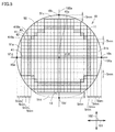
- FIG. 1 is a schematic plan view of the silicon carbide substrate 10 according to the first embodiment.
- the silicon carbide substrate 10 according to the first embodiment includes a first main surface 11.
- An orientation flat 13 is provided on the first main surface 11.
- the first main surface 11 includes both end portions 10a and 10b in the first radial direction 101.
- both ends 10a and 10b of the first main surface 11 in the first radial direction 101 are provided with a first virtual straight line 101a extending in the first radial direction 101 on the first main surface 11.
- it means two intersections of the first virtual straight line 101a and the peripheral edge of the first main surface 11.
- the first virtual straight line 101a is a virtual straight line extending in the first radial direction 101 through the center 45a of the first main surface 11.
- the center 45a of the first main surface 11 means the center when the shape of the first main surface 11 is a circle (for example, a circle before the orientation flat 13 is provided).
- the first radial direction 101 can be set, for example, in any direction of the first main surface 11.
- the first main surface 11 includes both ends 10c and 10d in the second radial direction 102.
- both ends 10c and 10d of the first main surface 11 in the second radial direction 102 are provided with a second virtual straight line 102a extending in the second radial direction on the first main surface 11.
- it means two intersections of the second virtual straight line 102a and the peripheral edge of the first main surface 11.
- the second virtual straight line 102a is a virtual straight line extending in the second radial direction 101 through the center 45a of the first main surface 11.
- the second radial direction 102 is a direction orthogonal to the first radial direction 101.
- the first main surface 11 includes first regions 51a and 51b within 5 mm inward from both end portions 10a and 10b of the first radial direction 101 of the first main surface 11.
- the first main surface 11 includes second regions 51c and 51d within 5 mm inward from both ends 10c and 10d of the first main surface 11 in the second radial direction 102.
- the first main surface 11 includes a central region 50 which is a region obtained by excluding the first regions 51a and 51b and the second regions 51c and 51d from the entire region of the first main surface 11.
- the central region 50 is divided into a plurality of square regions having a side of 5 mm, for example, as shown in FIG.
- the central region 50 is divided into a plurality of square regions so as to have the largest number of square regions having a side of 5 mm.
- As a square area only the area that constitutes a completely square is recognized. Areas that do not completely form a square due to lack of a part are not recognized as square areas.
- the first square region 41 is a square region that completely constitutes a square among a plurality of divided square regions of the central region 50, and is a square region located on the outermost side of the central region 50. means.
- the region 410a is located outside the central region 50 (peripheral side of the first main surface 11) with respect to the first square region 41 in the first radial direction 101.
- the region 410b is located outside the central region 50 with respect to the first square region 41 in the second radial direction 102.
- the regions 410a and 410b do not completely form a square, they are not recognized as square regions.
- the first square area 41 is certified as the first square area 41 constituting the outermost circumference.
- the central region 50 includes a plurality of first square regions 41.
- the plurality of first square regions 41 are arranged in a ring shape so as to form the outermost circumference of the plurality of square regions of the central region 50, for example, as shown in FIG.
- FIG. 2 is a schematic enlarged view of a cross section taken along the line II-II of FIG.
- FIG. 2 shows the LTV (Local Tickness Variation) of the first square region 41.
- the LTV of the first square region 41 is the second in the first square region 41 in a state where the second main surface 12 on the side opposite to the first main surface 11 is completely adsorbed on the flat suction surface. It is a value obtained by subtracting the height T1 from the second main surface 12 to the lowest point 41a of the first main surface 11 from the height T2 from the main surface 12 to the highest point 41b of the first main surface 11. ..
- LTV of the first square region 41 is calculated by the following formula (1).
- LTV of the first square area 41
- LTV is an index that quantitatively indicates the flatness of the first main surface 11 of the silicon carbide substrate 10.
- LTV can be measured by using, for example, "Tropel FlatMaster (registered trademark)" manufactured by Corning Tropel.
- the LTV is measured for each of the plurality of first square regions 41 constituting the outermost circumference of the plurality of square regions of the central region 50. Then, the average value of the LTV is calculated from the measured value of each LTV in the plurality of first square regions 41. The average value of the LTV is taken as the average value of the LTV of the plurality of first square regions 41 of the silicon carbide substrate 10 according to the first embodiment.
- the average value of the LTV of the plurality of first square regions 41 of the silicon carbide substrate 10 according to the first embodiment is 0.75 ⁇ m or less. This means that the flatness of the peripheral edge of the silicon carbide substrate 10 according to the first embodiment is improved as compared with the conventional silicon carbide substrate. As a result, in the silicon carbide substrate 10 according to the first embodiment, the device manufacturing area can be expanded to a region closer to the peripheral edge of the first main surface 11 of the silicon carbide substrate 10 as compared with the conventional silicon carbide substrate. Therefore, more devices can be manufactured from one silicon carbide substrate 10.
- FIG. 3 is a schematic plan view of the silicon carbide substrate 10 according to the second embodiment.
- the silicon carbide substrate 10 according to the second embodiment is characterized in that the average value of LTV in the second square region 42 is 0.4 ⁇ m or less.
- the second square region 42 is arranged inside the first radial direction 101 or inside the second radial direction 102 of each of the first square region 41 among the plurality of divided square regions of the central region 50. It is a square area formed, and is a square area located adjacent to the first square area 41.
- the plurality of divided square regions of the central region 50 include the plurality of second square regions 42.
- the second square region 42 is arranged in a ring shape so as to form the inner circumference of the ring formed by the first square region 41, for example, as shown in FIG.
- FIG. 4 is a schematic enlarged view of a cross section taken along the IV-IV of FIG.
- FIG. 4 shows the LTV of the second square area 42.
- the LTV of the second square region 42 is the second in the second square region 42 in a state where the second main surface 12 on the side opposite to the first main surface 11 is completely adsorbed on the flat suction surface. It is a value obtained by subtracting the height T3 from the second main surface 12 to the lowest point 42a of the first main surface 11 from the height T4 from the main surface 12 to the highest point 42b of the first main surface 11. ..
- the LTV of the second square region 42 is calculated by the following formula (2).
- LTV in the second square area 42
- the LTV is measured for each of the plurality of second square regions 42 arranged in a ring so as to form the inner circumference of the ring of the first square region 41.
- the average value of the LTV is calculated from the measured value of each LTV in the plurality of second square regions 42.
- the average value of the LTV is taken as the average value of the LTV of the plurality of second square regions 42 of the silicon carbide substrate 10 according to the second embodiment.
- the average value of the LTV of the plurality of second square regions 42 of the silicon carbide substrate 10 according to the second embodiment is 0.4 ⁇ m or less.
- the average value of the LTV of the second square region 42 is 0.4 ⁇ m or less, the average value of the LTV of the first square region 41 adjacent to the outside of the second square region 42 also tends to have a low value. It is in. This means that the flatness of the peripheral edge of the silicon carbide substrate 10 according to the second embodiment is improved.
- the device manufacturing area can be expanded to a region closer to the peripheral edge of the first main surface 11 of the silicon carbide substrate 10 as compared with the conventional silicon carbide substrate. More devices can be made from one silicon carbide substrate 10.
- FIG. 5 is a schematic plan view of the silicon carbide substrate 10 according to the third embodiment.
- the silicon carbide substrate 10 according to the third embodiment is characterized in that the average value of the LTV in the third square region 43 is 0.3 ⁇ m or less.
- the third square region 43 is arranged inside the first radial direction 101 or inside the second radial direction 102 of each of the second square region 42 among the plurality of divided square regions of the central region 50. It is a square area formed and is a square area located adjacent to the second square area 42.
- the plurality of divided square regions of the central region 50 include the plurality of third square regions 43.
- the third square region 43 is arranged in an annular shape so as to form the inner circumference of the ring formed by the second square region 42, for example, as shown in FIG.
- FIG. 6 is a schematic enlarged view of a cross section taken along the VI-VI of FIG.
- FIG. 6 shows the LTV of the third square area 43.
- the LTV of the third square region 43 is the second in the third square region 43 in a state where the second main surface 12 on the side opposite to the first main surface 11 is completely adsorbed on the flat suction surface. It is a value obtained by subtracting the height T5 from the second main surface 12 to the lowest point 43a of the first main surface 11 from the height T6 from the main surface 12 to the highest point 43b of the first main surface 11. ..
- the LTV of the third square region 43 is calculated by the following formula (3).
- LTV in the third square area 43
- the LTV is measured for each of the plurality of third square regions 43 arranged in a ring so as to form the inner circumference of the ring of the second square region 42.
- the average value of the LTV is calculated from the measured value of each LTV in the plurality of third square regions 43.
- the average value of the LTV is taken as the average value of the LTV of the plurality of third square regions 43 of the silicon carbide substrate 10 according to the third embodiment.
- the average value of the LTV of the plurality of third square regions 43 of the silicon carbide substrate 10 according to the third embodiment is 0.3 ⁇ m or less.
- the average value of the LTV of the third square region 43 is 0.3 ⁇ m or less, the average value of the LTV of the second square region 42 adjacent to the outside of the third square region 43 and the second square region
- the average value of the LTV of the first square region 41 adjacent to the outside of the 42 also tends to have a low value. This means that the flatness of the peripheral edge of the silicon carbide substrate 10 according to the third embodiment is improved.
- the device manufacturing area can be expanded to a region closer to the peripheral edge of the first main surface 11 of the silicon carbide substrate 10 as compared with the conventional silicon carbide substrate. More devices can be made from one silicon carbide substrate 10.
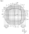
- FIG. 7 is a schematic plan view of the silicon carbide substrate 10 according to the fourth embodiment.
- the silicon carbide substrate 10 according to the fourth embodiment is characterized in that the average value of the LTV in the fourth square region 44 is 0.25 ⁇ m or less.
- the fourth square region 44 is arranged inside the first radial direction 101 or inside the second radial direction 102 of each of the third square region 43 among the plurality of divided square regions of the central region 50. It is a square area that is located adjacent to the third square area 43.
- the plurality of divided square regions of the central region 50 include a plurality of fourth square regions 44.
- the fourth square region 44 is arranged in an annular shape so as to form the inner circumference of the ring formed by the third square region 43, for example, as shown in FIG.
- FIG. 8 is a schematic enlarged view of a cross section along VIII-VIII of FIG.
- FIG. 8 shows the LTV of the fourth square area 44.
- the LTV of the fourth square region 44 is the second in the fourth square region 44 in a state where the second main surface 12 opposite to the first main surface 11 is completely adsorbed on the flat suction surface. It is a value obtained by subtracting the height T7 from the second main surface 12 to the lowest point 44a of the first main surface 11 from the height T8 from the main surface 12 to the highest point 44b of the first main surface 11. ..
- the LTV of the fourth square region 44 is calculated by the following formula (4).
- LTV in the fourth square area 44
- the LTV is measured for each of the plurality of fourth square regions 44 arranged in a ring so as to form the inner circumference of the ring of the third square region 43.
- the average value of the LTV is calculated from the measured value of each LTV in the plurality of fourth square regions 44.
- the average value of the LTV is taken as the average value of the LTV of the plurality of fourth square regions 44 of the silicon carbide substrate 10 according to the fourth embodiment.
- the average value of the LTV of the plurality of fourth square regions 44 of the silicon carbide substrate 10 according to the fourth embodiment is 0.25 ⁇ m or less.
- the average value of the LTV of the second square region 42 adjacent to the second square region 42 and the average value of the LTV of the first square region 41 adjacent to the outside of the second square region 42 also tend to have low values. This means that the flatness of the peripheral edge of the silicon carbide substrate 10 according to the third embodiment is improved.
- the manufacturing area of the device can be expanded to a region closer to the peripheral edge of the first main surface 11 of the silicon carbide substrate 10 as compared with the conventional silicon carbide substrate. Therefore, more devices can be manufactured from one silicon carbide substrate 10.
- FIG. 8 shows the LTV of the fifth square region 45 at the center 45a of the first main surface 11.
- the LTV of the fifth square region 45 is the second in the fifth square region 45 in a state where the second main surface 12 on the side opposite to the first main surface 11 is completely adsorbed on the flat suction surface. It is a value obtained by subtracting the height T9 from the second main surface 12 to the lowest point 45c of the first main surface 11 from the height T10 from the main surface 12 to the highest point 45b of the first main surface 11. .
- the fifth square region 45 is composed of a square having a side of 5 mm. The intersection of the diagonal lines of the squares constituting the fifth square region 45 is the center 45a.
- the LTV of the fifth square region 45 is calculated by the following formula (5).
- LTV in the fifth square area 45
- the first to fourth embodiments at least one region selected from the group consisting of the first square region 41, the second square region 42, the third square region 43, and the fourth square region 44.
- the average value of LTV can be 0.1 ⁇ m or more. Even in this case, the flatness of the peripheral edge of the silicon carbide substrate 10 according to the first to fourth embodiments tends to be improved.
- FIG. 9 is a flowchart of a method for manufacturing a silicon carbide substrate according to the fifth embodiment.
- the slicing step S1 is performed.
- the slicing step S1 can be performed, for example, by slicing an ingot made of a silicon carbide single crystal produced by a sublimation method with a wire saw.
- the chamfering step S2 is performed.
- the chamfering step S2 can be performed, for example, by scraping the corners of the silicon carbide single crystal wafer obtained in the slicing step S1.
- the rough polishing step S3 is performed.
- the rough polishing step S3 can be performed, for example, by mechanically polishing both main surfaces of the silicon carbide single crystal wafer after the chamfering step S2.
- Mechanical polishing includes, for example, grinding or wrapping.
- the first double-main surface chemical mechanical polishing step S4 is performed.
- both main surfaces of the silicon carbide single crystal wafer after the rough polishing step S3 are chemically mechanically polished (CMP: Chemical Mechanical Polishing). It can be done by applying.
- CMP Chemical Mechanical Polishing
- the first double-main surface chemical mechanical polishing step S4 is performed as follows. First, the polishing pads shown in Table 1 are installed on the respective surfaces of the upper surface plate and the lower surface plate. Next, the silicon carbide single crystal wafer is sandwiched between the polishing pad of the upper surface plate and the polishing pad of the lower surface plate, and the surface pressure shown in Table 1 is applied to the silicon carbide single crystal wafer. Next, while supplying the polishing liquids shown in Table 1 to the upper and lower main surfaces of the silicon carbide single crystal wafer, the upper surface plate and the lower surface plate are rotated in opposite directions at the platen rotation speeds shown in Table 1. . At this time, the silicon carbide single crystal wafer between the upper surface plate and the lower surface plate also rotates in the same direction as either the upper surface plate or the lower surface plate via the carrier.
- top: bottom 3: 2
- Relative speed ratio in Table 1 is carbonization of the upper platen for polishing the silicon surface (Si surface) which is the upper main surface of the silicon carbide single crystal wafer.
- the silicon carbide single crystal wafer rotates counterclockwise at a rotation speed of 6 rpm
- the lower platen rotates counterclockwise at a rotation speed of 30 rpm.
- the second double-main surface chemical mechanical polishing step S5 is performed.
- chemical mechanical polishing is performed on both main surfaces of the silicon carbide single crystal wafer after the first double-main surface chemical mechanical polishing step S4 under the conditions shown in Table 2 below. It can be done by applying.
- the second double-main surface chemical mechanical polishing step S5 is performed in the same manner as the first double-main surface chemical mechanical polishing step S4, except that the polishing liquid and the polishing pad are changed to the conditions shown in Table 2.
- FIG. 10 is a schematic plan view of the entire surface of an example of the polishing pad 34 used in the first double-main surface chemical mechanical polishing step S4 and the second double-main surface chemical mechanical polishing step S5.
- the entire donut-shaped surface of the polishing cloth 34 has a silicon carbide single crystal formed by the polishing cloth 34 on an effective polishing surface 34a that contributes to polishing the main surface of the silicon carbide single crystal wafer by the polishing cloth 34. It has a configuration in which grid-like grooves 34b that do not contribute to polishing the main surface of the wafer are provided.
- the effective surface ratio A si of the polishing cloth 34 for polishing the Si surface and the effective surface ratio A c of the polishing cloth 34 for polishing the C surface are obtained.
- a si ⁇ 80 and Ac ⁇ 80 ... Equation (6) A si > 90 and Ac ⁇ 90 ... Equation (7) 1 ⁇ (A si / Ac ) ⁇ 1.25 ... Equation (8) 1.02 ⁇ (A si / A c ) ⁇ 1.05 ... formula (9)
- the effective surface area ratio A si [%] of the polishing pad 34 for polishing the Si surface of the silicon carbide single crystal wafer can be calculated by the following formula (10).
- Effective surface area ratio A si [%] 100 ⁇ ⁇ (Area of effective polishing surface 34a of polishing cloth 34 for polishing Si surface of silicon carbide single crystal wafer [mm 2 ]) / (Overall surface of polishing cloth 34 Area [mm 2 ]) ⁇ ... Equation (10)
- the effective surface area ratio A c [%] of the polishing pad 34 for polishing the C surface of the silicon carbide single crystal wafer can be calculated by the following formula (11).
- Effective surface area ratio A c [%] 100 ⁇ ⁇ (Area of effective polishing surface 34a of polishing cloth 34 for polishing C surface of silicon carbide single crystal wafer [mm 2 ]) / (Overall surface of polishing cloth 34 Area [mm 2 ]) ⁇ ... Equation (11)
- the area [mm 2 ] of the entire surface of the polishing pad 34 in the above formulas (10) and (11) is, for example, as shown in FIG. 10, the polishing pad 34 when the surface of the polishing pad 34 is viewed in a plan view. Means the total area of the surface of.
- the ratio (R si / R c ) of the polishing rate R si of the Si surface of the silicon carbide single crystal wafer to the polishing rate R c of the C surface is 0.6 or more and 1.4 or less. It is more preferably 0.7 or more and 1.3 or less, and even more preferably 0.8 or more and 1.2 or less.
- the polishing rate means the amount of silicon carbide single crystal wafers polished per unit time. The polishing rate can be adjusted, for example, by adjusting the polishing conditions.
- FIG. 11 is a flowchart of a method for manufacturing a silicon carbide substrate according to the sixth embodiment.
- the slicing step S1, the chamfering step S2, the rough polishing step S3, and the first both main surface chemical mechanical polishing steps S4 are performed in this order. .. Since the description of these steps is the same as the content described in the fifth embodiment, the description thereof will be omitted.
- the single main surface chemical mechanical polishing step S5a is performed.
- the Si surface and the C surface of the silicon carbide single crystal wafer after the first double main surface chemical mechanical polishing step S4 are chemically mechanically polished one by one. It can be done by applying.
- the single main surface chemical mechanical polishing step S5a is performed as follows. First, the polishing pad shown in Table 3 is installed on the surface of the surface plate. Next, the main surface of the silicon carbide single crystal wafer is held by the polishing head so as to face the polishing pad. Next, the polishing liquid shown in Table 3 is supplied between the polishing pad and the main surface of the silicon carbide single crystal wafer. Next, the surface pressure shown in Table 3 is applied to the silicon carbide single crystal wafer. Here, the main surface of the silicon carbide single crystal wafer on the polished side is brought into contact with the polishing pad. Next, the surface plate and the polishing head are rotated in the same direction at the surface plate rotation speeds shown in Table 3. This operation is performed on each main surface of the silicon carbide single crystal wafer.
- Example 1 the silicon carbide substrate was manufactured according to the flowchart of the method for manufacturing the silicon carbide substrate shown in FIG. Specifically, a silicon carbide substrate was manufactured as follows.
- the slicing step S1 was performed by slicing an ingot made of a silicon carbide single crystal produced by the sublimation method with a wire saw.
- the chamfering step S2 was performed by scraping the corners of the silicon carbide single crystal wafer obtained in the slicing step S1.
- the rough polishing step S3 was performed by mechanically polishing both main surfaces of the silicon carbide single crystal wafer after the chamfering step S2.
- both main surfaces of the silicon carbide single crystal wafer after the rough polishing step S3 are subjected to chemical mechanical polishing to perform chemical mechanical polishing on both main surfaces.
- the polishing step S4 was performed.
- Example 2 the silicon carbide substrate was manufactured according to the flowchart of the method for manufacturing the silicon carbide substrate shown in FIG. That is, in Experimental Example 2, the same as in Experimental Example 1 except that the single main surface chemical mechanical polishing step S5a was performed instead of the second double main surface chemical mechanical polishing step S5 of Experimental Example 1. The silicon carbide substrate of 2 was manufactured.
- the silicon carbide substrate becomes flatter as it progresses from the center to the periphery of the silicon carbide substrate as compared with the silicon carbide substrate of Experimental Example 3. You can see that there is.
- the silicon carbide substrate of Experimental Example 1 has a flatter silicon carbide substrate as it progresses from the center to the periphery of the silicon carbide substrate as compared with the silicon carbide substrate of Experimental Example 2. I understand.
- Si of the silicon carbide single crystal wafer in the first double-sided chemical mechanical polishing step S4 in Experimental Example 1 The ratio (R si / R c ) of the surface polishing rate (R si ) to the C surface polishing rate (R c ) is preferably 0.6 or more and 1.4 or less, preferably 0.7 or more and 1.3. It can be seen that the setting is more preferably 0.8 or more and 1.2 or less.
- the values in the second row from the top of Table 7 (1.10, 1.00, 0.70, 0.60, 0.47, 0.40, and 0.30) are the Si planes of the silicon carbide single crystal wafer.
- the polishing rate (R si ) of is shown.
- the values in the second column from the left in Table 7 (1.80, 1.35, 1.15, 0.94, 0.80, and 0.60) are the polishing rates of the C surface of the silicon carbide single crystal wafer (1.80, 1.35, 1.15, 0.94, 0.80, and 0.60).
- R c is shown.
- the values in the second row from the top of Table 8 (0.27, 0.26, 0.24, 0.20, 0.19, 0.17, and 0.13) are the Si surfaces of the silicon carbide single crystal wafer.
- the polishing rate (R si ) is shown.
- the values in the second column from the left in Table 8 (0.62, 0.49, 0.46, 0.40, 0.32, and 0.25) are the polishing rates (R) of the C surface of the silicon carbide single crystal wafer.
- c is shown. Numerical values other than these in Table 8 indicate the ratio (R si / R c ) of the polishing rate R si of the Si surface of the silicon carbide single crystal wafer to the polishing rate R c of the C surface.
- the notations A to E in Table 8 show the results of evaluating the state of the silicon carbide single crystal wafer according to the above criteria.
- the values in the second row from the top of Table 9 (99.7, 97.7, 93.2, 90.0, 86.9, 80.8, and 63.8) indicate the Si surface of the silicon carbide single crystal wafer.
- the effective surface area ratio A si [%] of the polishing pad for polishing is shown.
- the values in the second column from the left in Table 9 (98.0, 93.5, 90.3, 87.2, 81.1, and 64.1) are for polishing the C surface of the silicon carbide single crystal wafer.
- the effective surface area ratio Ac [%] of the polishing pad is shown.
- the values other than these in Table 9 are the effective surface ratio A si [%] of the polishing cloth for polishing the Si surface of the silicon carbide single crystal wafer and the polishing cloth for polishing the C surface of the silicon carbide single crystal wafer.
- the ratio (A si / Ac ) to the effective surface ratio A c [%] is shown.
- the notations A to E in Table 9 show the results of evaluating the state of the silicon carbide single crystal wafer according to the same criteria as in Experimental Example 5.
Landscapes
- Chemical & Material Sciences (AREA)
- Engineering & Computer Science (AREA)
- Crystallography & Structural Chemistry (AREA)
- Materials Engineering (AREA)
- Metallurgy (AREA)
- Organic Chemistry (AREA)
- Inorganic Chemistry (AREA)
- Mechanical Engineering (AREA)
- Crystals, And After-Treatments Of Crystals (AREA)
- Mechanical Treatment Of Semiconductor (AREA)
Priority Applications (3)
| Application Number | Priority Date | Filing Date | Title |
|---|---|---|---|
| CN202080042958.0A CN114026672B (zh) | 2019-06-13 | 2020-05-27 | 碳化硅衬底和碳化硅衬底的制造方法 |
| JP2021525982A JPWO2020250678A1 (https=) | 2019-06-13 | 2020-05-27 | |
| US17/617,126 US20220170179A1 (en) | 2019-06-13 | 2020-05-27 | Silicon carbide substrate and method of manufacturing silicon carbide substrate |
Applications Claiming Priority (2)
| Application Number | Priority Date | Filing Date | Title |
|---|---|---|---|
| JP2019110318 | 2019-06-13 | ||
| JP2019-110318 | 2019-06-13 |
Publications (1)
| Publication Number | Publication Date |
|---|---|
| WO2020250678A1 true WO2020250678A1 (ja) | 2020-12-17 |
Family
ID=73781911
Family Applications (1)
| Application Number | Title | Priority Date | Filing Date |
|---|---|---|---|
| PCT/JP2020/020904 Ceased WO2020250678A1 (ja) | 2019-06-13 | 2020-05-27 | 炭化珪素基板および炭化珪素基板の製造方法 |
Country Status (5)
| Country | Link |
|---|---|
| US (1) | US20220170179A1 (https=) |
| JP (1) | JPWO2020250678A1 (https=) |
| CN (1) | CN114026672B (https=) |
| TW (1) | TW202123328A (https=) |
| WO (1) | WO2020250678A1 (https=) |
Citations (8)
| Publication number | Priority date | Publication date | Assignee | Title |
|---|---|---|---|---|
| JP2008535761A (ja) * | 2005-04-07 | 2008-09-04 | クリー インコーポレイテッド | 歪み、反り、及びttvが少ない75ミリメートル炭化珪素ウェハ |
| JP2010029996A (ja) * | 2008-07-30 | 2010-02-12 | Toray Ind Inc | 研磨パッド |
| JP2011035023A (ja) * | 2009-07-30 | 2011-02-17 | Nippon Steel Corp | 半導体基板の研磨方法及び研磨装置 |
| JP2015005702A (ja) * | 2013-06-24 | 2015-01-08 | 昭和電工株式会社 | SiC基板の製造方法 |
| JP2015229748A (ja) * | 2014-06-06 | 2015-12-21 | コニカミノルタ株式会社 | Cmp用研磨液 |
| JP2016501809A (ja) * | 2012-10-26 | 2016-01-21 | ダウ コーニング コーポレーションDow Corning Corporation | 平坦なSiC半導体基板 |
| JP2016124043A (ja) * | 2014-12-26 | 2016-07-11 | 東洋ゴム工業株式会社 | 研磨パッド |
| JP2016210680A (ja) * | 2015-05-11 | 2016-12-15 | 住友電気工業株式会社 | 炭化珪素単結晶基板、炭化珪素半導体装置および炭化珪素半導体装置の製造方法 |
Family Cites Families (21)
| Publication number | Priority date | Publication date | Assignee | Title |
|---|---|---|---|---|
| JP3410925B2 (ja) * | 1997-05-23 | 2003-05-26 | ロデール・ニッタ株式会社 | 両面研磨機のキャリア |
| KR100533528B1 (ko) * | 2000-11-16 | 2005-12-05 | 신에츠 한도타이 가부시키가이샤 | 웨이퍼의 형상 평가방법 및 장치 및 디바이스의 제조방법,웨이퍼 및 웨이퍼의 선별방법 |
| WO2009139140A1 (ja) * | 2008-05-13 | 2009-11-19 | パナソニック株式会社 | 半導体素子 |
| TWI510449B (zh) * | 2010-06-22 | 2015-12-01 | Sumitomo Electric Industries | Manufacturing method of light emitting element |
| JP5621702B2 (ja) * | 2011-04-26 | 2014-11-12 | 信越半導体株式会社 | 半導体ウェーハ及びその製造方法 |
| JP6083129B2 (ja) * | 2012-04-27 | 2017-02-22 | 富士電機株式会社 | 半導体装置の製造方法および製造装置 |
| JP2014203833A (ja) * | 2013-04-01 | 2014-10-27 | 住友電気工業株式会社 | 炭化珪素半導体装置の製造方法 |
| JP5803979B2 (ja) * | 2013-05-29 | 2015-11-04 | 住友電気工業株式会社 | 炭化珪素基板および炭化珪素半導体装置ならびに炭化珪素基板および炭化珪素半導体装置の製造方法 |
| JP6107453B2 (ja) * | 2013-06-13 | 2017-04-05 | 住友電気工業株式会社 | 炭化珪素半導体装置の製造方法 |
| US9508611B2 (en) * | 2013-08-14 | 2016-11-29 | Hitachi, Ltd. | Semiconductor inspection method, semiconductor inspection device and manufacturing method of semiconductor element |
| JP2015053428A (ja) * | 2013-09-09 | 2015-03-19 | 住友電気工業株式会社 | 炭化珪素半導体装置の製造方法 |
| JP5839069B2 (ja) * | 2014-03-28 | 2016-01-06 | 住友電気工業株式会社 | 炭化珪素単結晶基板、炭化珪素エピタキシャル基板およびこれらの製造方法 |
| JP6331634B2 (ja) * | 2014-04-17 | 2018-05-30 | 住友電気工業株式会社 | 炭化珪素半導体装置の製造方法 |
| JP6623759B2 (ja) * | 2014-09-08 | 2019-12-25 | 住友電気工業株式会社 | 炭化珪素単結晶基板およびその製造方法 |
| JP6287774B2 (ja) * | 2014-11-19 | 2018-03-07 | 住友電気工業株式会社 | 炭化珪素半導体装置の製造方法 |
| JP2016028009A (ja) * | 2015-09-02 | 2016-02-25 | 住友電気工業株式会社 | 炭化珪素基板および炭化珪素半導体装置ならびに炭化珪素基板および炭化珪素半導体装置の製造方法 |
| JP6619685B2 (ja) * | 2016-04-19 | 2019-12-11 | 株式会社ディスコ | SiCウエーハの加工方法 |
| JP6497358B2 (ja) * | 2016-06-22 | 2019-04-10 | 株式会社デンソー | 炭化珪素半導体装置の製造方法 |
| JP6748572B2 (ja) * | 2016-12-28 | 2020-09-02 | 昭和電工株式会社 | p型SiCエピタキシャルウェハ及びその製造方法 |
| JP7012454B2 (ja) * | 2017-04-27 | 2022-01-28 | 株式会社岡本工作機械製作所 | 静電吸着チャックの製造方法並びに半導体装置の製造方法 |
| US11322349B2 (en) * | 2017-05-19 | 2022-05-03 | Sumitomo Electric Industries, Ltd. | Silicon carbide substrate and silicon carbide epitaxial substrate |
-
2020
- 2020-05-27 CN CN202080042958.0A patent/CN114026672B/zh active Active
- 2020-05-27 WO PCT/JP2020/020904 patent/WO2020250678A1/ja not_active Ceased
- 2020-05-27 JP JP2021525982A patent/JPWO2020250678A1/ja active Pending
- 2020-05-27 US US17/617,126 patent/US20220170179A1/en not_active Abandoned
- 2020-06-11 TW TW109119736A patent/TW202123328A/zh unknown
Patent Citations (8)
| Publication number | Priority date | Publication date | Assignee | Title |
|---|---|---|---|---|
| JP2008535761A (ja) * | 2005-04-07 | 2008-09-04 | クリー インコーポレイテッド | 歪み、反り、及びttvが少ない75ミリメートル炭化珪素ウェハ |
| JP2010029996A (ja) * | 2008-07-30 | 2010-02-12 | Toray Ind Inc | 研磨パッド |
| JP2011035023A (ja) * | 2009-07-30 | 2011-02-17 | Nippon Steel Corp | 半導体基板の研磨方法及び研磨装置 |
| JP2016501809A (ja) * | 2012-10-26 | 2016-01-21 | ダウ コーニング コーポレーションDow Corning Corporation | 平坦なSiC半導体基板 |
| JP2015005702A (ja) * | 2013-06-24 | 2015-01-08 | 昭和電工株式会社 | SiC基板の製造方法 |
| JP2015229748A (ja) * | 2014-06-06 | 2015-12-21 | コニカミノルタ株式会社 | Cmp用研磨液 |
| JP2016124043A (ja) * | 2014-12-26 | 2016-07-11 | 東洋ゴム工業株式会社 | 研磨パッド |
| JP2016210680A (ja) * | 2015-05-11 | 2016-12-15 | 住友電気工業株式会社 | 炭化珪素単結晶基板、炭化珪素半導体装置および炭化珪素半導体装置の製造方法 |
Also Published As
| Publication number | Publication date |
|---|---|
| CN114026672B (zh) | 2025-03-11 |
| JPWO2020250678A1 (https=) | 2020-12-17 |
| US20220170179A1 (en) | 2022-06-02 |
| CN114026672A (zh) | 2022-02-08 |
| TW202123328A (zh) | 2021-06-16 |
Similar Documents
| Publication | Publication Date | Title |
|---|---|---|
| US20110250826A1 (en) | Pad conditioner having reduced friction and method of manufacturing the same | |
| JP2010021487A (ja) | 半導体ウェーハおよびその製造方法 | |
| JP2019210206A (ja) | 面取り炭化ケイ素基板および面取り方法 | |
| JP6981469B2 (ja) | 炭化珪素基板および炭化珪素エピタキシャル基板 | |
| CN113439008B (zh) | 晶片制造方法以及晶片 | |
| CN109414799B (zh) | 双面研磨装置 | |
| WO2009104224A1 (ja) | 研磨布用ドレッサー | |
| CN1795545A (zh) | 半导体晶片的制造方法 | |
| CN114667594A (zh) | 晶片的研磨方法及硅晶片 | |
| WO2020250678A1 (ja) | 炭化珪素基板および炭化珪素基板の製造方法 | |
| JP7359203B2 (ja) | 酸化ガリウム基板、および酸化ガリウム基板の製造方法 | |
| CN112405337B (zh) | 一种抛光垫及半导体器件的制造方法 | |
| JP6229807B1 (ja) | マスクブランク | |
| JP6825733B1 (ja) | 半導体ウェーハの製造方法 | |
| CN110312592A (zh) | 用于对玻璃片的边缘进行精整的方法和设备 | |
| CN112757154A (zh) | 一种抛光垫 | |
| KR101211138B1 (ko) | 연약패드용 컨디셔너 및 그 제조방법 | |
| JPS60249568A (ja) | 半導体ウエハの研磨方法 | |
| JP2020011853A (ja) | 再生基板の製造方法 | |
| CN117460597A (zh) | 具有凸多边形磨料部件的双面研磨设备 | |
| JP2019042896A (ja) | 両面研磨装置用の被研磨物保持用キャリア | |
| US20240198481A1 (en) | Pad conditioner with pyramids of single-crystal diamond | |
| CN111993295A (zh) | 一种带有一粗四精沟槽的砂轮及其应用 | |
| CN211992445U (zh) | 一种化学机械抛光垫 | |
| KR100933850B1 (ko) | 태양전지용 잉곳의 코너부 가공방법 및 장치와 그에 따라제조된 태양전지용 잉곳 및 웨이퍼 |
Legal Events
| Date | Code | Title | Description |
|---|---|---|---|
| 121 | Ep: the epo has been informed by wipo that ep was designated in this application |
Ref document number: 20823363 Country of ref document: EP Kind code of ref document: A1 |
|
| ENP | Entry into the national phase |
Ref document number: 2021525982 Country of ref document: JP Kind code of ref document: A |
|
| NENP | Non-entry into the national phase |
Ref country code: DE |
|
| 122 | Ep: pct application non-entry in european phase |
Ref document number: 20823363 Country of ref document: EP Kind code of ref document: A1 |
|
| WWG | Wipo information: grant in national office |
Ref document number: 202080042958.0 Country of ref document: CN |