WO2020241645A1 - 多層配線基板及びその製造方法 - Google Patents
多層配線基板及びその製造方法 Download PDFInfo
- Publication number
- WO2020241645A1 WO2020241645A1 PCT/JP2020/020760 JP2020020760W WO2020241645A1 WO 2020241645 A1 WO2020241645 A1 WO 2020241645A1 JP 2020020760 W JP2020020760 W JP 2020020760W WO 2020241645 A1 WO2020241645 A1 WO 2020241645A1
- Authority
- WO
- WIPO (PCT)
- Prior art keywords
- layer
- via hole
- metal wiring
- metal
- forming
- Prior art date
- Legal status (The legal status is an assumption and is not a legal conclusion. Google has not performed a legal analysis and makes no representation as to the accuracy of the status listed.)
- Ceased
Links
Images


Classifications
-
- H—ELECTRICITY
- H05—ELECTRIC TECHNIQUES NOT OTHERWISE PROVIDED FOR
- H05K—PRINTED CIRCUITS; CASINGS OR CONSTRUCTIONAL DETAILS OF ELECTRIC APPARATUS; MANUFACTURE OF ASSEMBLAGES OF ELECTRICAL COMPONENTS
- H05K1/00—Printed circuits
- H05K1/02—Details
- H05K1/11—Printed elements for providing electric connections to or between printed circuits
- H05K1/115—Via connections; Lands around holes or via connections
- H05K1/116—Lands, clearance holes or other lay-out details concerning the surrounding of a via
-
- H—ELECTRICITY
- H05—ELECTRIC TECHNIQUES NOT OTHERWISE PROVIDED FOR
- H05K—PRINTED CIRCUITS; CASINGS OR CONSTRUCTIONAL DETAILS OF ELECTRIC APPARATUS; MANUFACTURE OF ASSEMBLAGES OF ELECTRICAL COMPONENTS
- H05K3/00—Apparatus or processes for manufacturing printed circuits
- H05K3/40—Forming printed elements for providing electric connections to or between printed circuits
- H05K3/42—Plated through-holes or plated via connections
- H05K3/421—Blind plated via connections
-
- H—ELECTRICITY
- H05—ELECTRIC TECHNIQUES NOT OTHERWISE PROVIDED FOR
- H05K—PRINTED CIRCUITS; CASINGS OR CONSTRUCTIONAL DETAILS OF ELECTRIC APPARATUS; MANUFACTURE OF ASSEMBLAGES OF ELECTRICAL COMPONENTS
- H05K1/00—Printed circuits
- H05K1/02—Details
- H05K1/0296—Conductive pattern lay-out details not covered by sub groups H05K1/02 - H05K1/0295
- H05K1/0298—Multilayer circuits
-
- H—ELECTRICITY
- H05—ELECTRIC TECHNIQUES NOT OTHERWISE PROVIDED FOR
- H05K—PRINTED CIRCUITS; CASINGS OR CONSTRUCTIONAL DETAILS OF ELECTRIC APPARATUS; MANUFACTURE OF ASSEMBLAGES OF ELECTRICAL COMPONENTS
- H05K1/00—Printed circuits
- H05K1/02—Details
- H05K1/11—Printed elements for providing electric connections to or between printed circuits
- H05K1/115—Via connections; Lands around holes or via connections
-
- H—ELECTRICITY
- H05—ELECTRIC TECHNIQUES NOT OTHERWISE PROVIDED FOR
- H05K—PRINTED CIRCUITS; CASINGS OR CONSTRUCTIONAL DETAILS OF ELECTRIC APPARATUS; MANUFACTURE OF ASSEMBLAGES OF ELECTRICAL COMPONENTS
- H05K3/00—Apparatus or processes for manufacturing printed circuits
- H05K3/02—Apparatus or processes for manufacturing printed circuits in which the conductive material is applied to the surface of the insulating support and is thereafter removed from such areas of the surface which are not intended for current conducting or shielding
- H05K3/06—Apparatus or processes for manufacturing printed circuits in which the conductive material is applied to the surface of the insulating support and is thereafter removed from such areas of the surface which are not intended for current conducting or shielding the conductive material being removed chemically or electrolytically, e.g. by photo-etch process
- H05K3/07—Apparatus or processes for manufacturing printed circuits in which the conductive material is applied to the surface of the insulating support and is thereafter removed from such areas of the surface which are not intended for current conducting or shielding the conductive material being removed chemically or electrolytically, e.g. by photo-etch process being removed electrolytically
-
- H—ELECTRICITY
- H05—ELECTRIC TECHNIQUES NOT OTHERWISE PROVIDED FOR
- H05K—PRINTED CIRCUITS; CASINGS OR CONSTRUCTIONAL DETAILS OF ELECTRIC APPARATUS; MANUFACTURE OF ASSEMBLAGES OF ELECTRICAL COMPONENTS
- H05K3/00—Apparatus or processes for manufacturing printed circuits
- H05K3/10—Apparatus or processes for manufacturing printed circuits in which conductive material is applied to the insulating support in such a manner as to form the desired conductive pattern
- H05K3/18—Apparatus or processes for manufacturing printed circuits in which conductive material is applied to the insulating support in such a manner as to form the desired conductive pattern using precipitation techniques to apply the conductive material
-
- H—ELECTRICITY
- H05—ELECTRIC TECHNIQUES NOT OTHERWISE PROVIDED FOR
- H05K—PRINTED CIRCUITS; CASINGS OR CONSTRUCTIONAL DETAILS OF ELECTRIC APPARATUS; MANUFACTURE OF ASSEMBLAGES OF ELECTRICAL COMPONENTS
- H05K3/00—Apparatus or processes for manufacturing printed circuits
- H05K3/22—Secondary treatment of printed circuits
- H05K3/26—Cleaning or polishing of the conductive pattern
-
- H—ELECTRICITY
- H05—ELECTRIC TECHNIQUES NOT OTHERWISE PROVIDED FOR
- H05K—PRINTED CIRCUITS; CASINGS OR CONSTRUCTIONAL DETAILS OF ELECTRIC APPARATUS; MANUFACTURE OF ASSEMBLAGES OF ELECTRICAL COMPONENTS
- H05K3/00—Apparatus or processes for manufacturing printed circuits
- H05K3/46—Manufacturing multilayer circuits
- H05K3/4644—Manufacturing multilayer circuits by building the multilayer layer by layer, i.e. build-up multilayer circuits
- H05K3/467—Adding a circuit layer by thin film methods
-
- H—ELECTRICITY
- H05—ELECTRIC TECHNIQUES NOT OTHERWISE PROVIDED FOR
- H05K—PRINTED CIRCUITS; CASINGS OR CONSTRUCTIONAL DETAILS OF ELECTRIC APPARATUS; MANUFACTURE OF ASSEMBLAGES OF ELECTRICAL COMPONENTS
- H05K2201/00—Indexing scheme relating to printed circuits covered by H05K1/00
- H05K2201/03—Conductive materials
- H05K2201/0332—Structure of the conductor
- H05K2201/0335—Layered conductors or foils
- H05K2201/0338—Layered conductor, e.g. layered metal substrate, layered finish layer or layered thin film adhesion layer
-
- H—ELECTRICITY
- H05—ELECTRIC TECHNIQUES NOT OTHERWISE PROVIDED FOR
- H05K—PRINTED CIRCUITS; CASINGS OR CONSTRUCTIONAL DETAILS OF ELECTRIC APPARATUS; MANUFACTURE OF ASSEMBLAGES OF ELECTRICAL COMPONENTS
- H05K2201/00—Indexing scheme relating to printed circuits covered by H05K1/00
- H05K2201/03—Conductive materials
- H05K2201/0332—Structure of the conductor
- H05K2201/0335—Layered conductors or foils
- H05K2201/0344—Electroless sublayer, e.g. Ni, Co, Cd or Ag; Transferred electroless sublayer
-
- H—ELECTRICITY
- H05—ELECTRIC TECHNIQUES NOT OTHERWISE PROVIDED FOR
- H05K—PRINTED CIRCUITS; CASINGS OR CONSTRUCTIONAL DETAILS OF ELECTRIC APPARATUS; MANUFACTURE OF ASSEMBLAGES OF ELECTRICAL COMPONENTS
- H05K2201/00—Indexing scheme relating to printed circuits covered by H05K1/00
- H05K2201/09—Shape and layout
- H05K2201/09209—Shape and layout details of conductors
- H05K2201/095—Conductive through-holes or vias
- H05K2201/09509—Blind vias, i.e. vias having one side closed
-
- H—ELECTRICITY
- H05—ELECTRIC TECHNIQUES NOT OTHERWISE PROVIDED FOR
- H05K—PRINTED CIRCUITS; CASINGS OR CONSTRUCTIONAL DETAILS OF ELECTRIC APPARATUS; MANUFACTURE OF ASSEMBLAGES OF ELECTRICAL COMPONENTS
- H05K2201/00—Indexing scheme relating to printed circuits covered by H05K1/00
- H05K2201/09—Shape and layout
- H05K2201/09209—Shape and layout details of conductors
- H05K2201/095—Conductive through-holes or vias
- H05K2201/09545—Plated through-holes or blind vias without lands
-
- H—ELECTRICITY
- H05—ELECTRIC TECHNIQUES NOT OTHERWISE PROVIDED FOR
- H05K—PRINTED CIRCUITS; CASINGS OR CONSTRUCTIONAL DETAILS OF ELECTRIC APPARATUS; MANUFACTURE OF ASSEMBLAGES OF ELECTRICAL COMPONENTS
- H05K2201/00—Indexing scheme relating to printed circuits covered by H05K1/00
- H05K2201/09—Shape and layout
- H05K2201/09209—Shape and layout details of conductors
- H05K2201/09654—Shape and layout details of conductors covering at least two types of conductors provided for in H05K2201/09218 - H05K2201/095
- H05K2201/09745—Recess in conductor, e.g. in pad or in metallic substrate
-
- H—ELECTRICITY
- H05—ELECTRIC TECHNIQUES NOT OTHERWISE PROVIDED FOR
- H05K—PRINTED CIRCUITS; CASINGS OR CONSTRUCTIONAL DETAILS OF ELECTRIC APPARATUS; MANUFACTURE OF ASSEMBLAGES OF ELECTRICAL COMPONENTS
- H05K2201/00—Indexing scheme relating to printed circuits covered by H05K1/00
- H05K2201/09—Shape and layout
- H05K2201/09818—Shape or layout details not covered by a single group of H05K2201/09009 - H05K2201/09809
- H05K2201/09827—Tapered, e.g. tapered hole, via or groove
-
- H—ELECTRICITY
- H05—ELECTRIC TECHNIQUES NOT OTHERWISE PROVIDED FOR
- H05K—PRINTED CIRCUITS; CASINGS OR CONSTRUCTIONAL DETAILS OF ELECTRIC APPARATUS; MANUFACTURE OF ASSEMBLAGES OF ELECTRICAL COMPONENTS
- H05K2201/00—Indexing scheme relating to printed circuits covered by H05K1/00
- H05K2201/09—Shape and layout
- H05K2201/09818—Shape or layout details not covered by a single group of H05K2201/09009 - H05K2201/09809
- H05K2201/09845—Stepped hole, via, edge, bump or conductor
-
- H—ELECTRICITY
- H05—ELECTRIC TECHNIQUES NOT OTHERWISE PROVIDED FOR
- H05K—PRINTED CIRCUITS; CASINGS OR CONSTRUCTIONAL DETAILS OF ELECTRIC APPARATUS; MANUFACTURE OF ASSEMBLAGES OF ELECTRICAL COMPONENTS
- H05K2203/00—Indexing scheme relating to apparatus or processes for manufacturing printed circuits covered by H05K3/00
- H05K2203/05—Patterning and lithography; Masks; Details of resist
- H05K2203/0502—Patterning and lithography
- H05K2203/054—Continuous temporary metal layer over resist, e.g. for selective electroplating
-
- H—ELECTRICITY
- H05—ELECTRIC TECHNIQUES NOT OTHERWISE PROVIDED FOR
- H05K—PRINTED CIRCUITS; CASINGS OR CONSTRUCTIONAL DETAILS OF ELECTRIC APPARATUS; MANUFACTURE OF ASSEMBLAGES OF ELECTRICAL COMPONENTS
- H05K3/00—Apparatus or processes for manufacturing printed circuits
- H05K3/0011—Working of insulating substrates or insulating layers
- H05K3/0017—Etching of the substrate by chemical or physical means
- H05K3/0026—Etching of the substrate by chemical or physical means by laser ablation
- H05K3/0032—Etching of the substrate by chemical or physical means by laser ablation of organic insulating material
- H05K3/0035—Etching of the substrate by chemical or physical means by laser ablation of organic insulating material of blind holes, i.e. having a metal layer at the bottom
-
- H—ELECTRICITY
- H05—ELECTRIC TECHNIQUES NOT OTHERWISE PROVIDED FOR
- H05K—PRINTED CIRCUITS; CASINGS OR CONSTRUCTIONAL DETAILS OF ELECTRIC APPARATUS; MANUFACTURE OF ASSEMBLAGES OF ELECTRICAL COMPONENTS
- H05K3/00—Apparatus or processes for manufacturing printed circuits
- H05K3/10—Apparatus or processes for manufacturing printed circuits in which conductive material is applied to the insulating support in such a manner as to form the desired conductive pattern
- H05K3/108—Apparatus or processes for manufacturing printed circuits in which conductive material is applied to the insulating support in such a manner as to form the desired conductive pattern by semi-additive methods; masks therefor
-
- H—ELECTRICITY
- H05—ELECTRIC TECHNIQUES NOT OTHERWISE PROVIDED FOR
- H05K—PRINTED CIRCUITS; CASINGS OR CONSTRUCTIONAL DETAILS OF ELECTRIC APPARATUS; MANUFACTURE OF ASSEMBLAGES OF ELECTRICAL COMPONENTS
- H05K3/00—Apparatus or processes for manufacturing printed circuits
- H05K3/38—Improvement of the adhesion between the insulating substrate and the metal
- H05K3/388—Improvement of the adhesion between the insulating substrate and the metal by the use of a metallic or inorganic thin film adhesion layer
-
- H—ELECTRICITY
- H05—ELECTRIC TECHNIQUES NOT OTHERWISE PROVIDED FOR
- H05K—PRINTED CIRCUITS; CASINGS OR CONSTRUCTIONAL DETAILS OF ELECTRIC APPARATUS; MANUFACTURE OF ASSEMBLAGES OF ELECTRICAL COMPONENTS
- H05K3/00—Apparatus or processes for manufacturing printed circuits
- H05K3/46—Manufacturing multilayer circuits
- H05K3/4644—Manufacturing multilayer circuits by building the multilayer layer by layer, i.e. build-up multilayer circuits
Definitions
- the present invention is a technique relating to a multilayer wiring board.
- a multi-layer wiring board having a structure in which a circuit pattern composed of metal wiring layers is multi-layered and an insulating resin is interposed between the layers of each circuit pattern is used as the circuit density is increased. May be done.
- a method is known in which a bottomed hole (via hole) is formed in an insulating layer on the board, and circuit patterns (metal wiring layers) of different layers are electrically connected through the bottomed hole.
- this type of multilayer wiring substrate is formed by laminating a conductive layer (metal wiring layer) and an insulating layer in order, and electrical connection between circuit patterns of each conductive layer is formed between circuit patterns as needed. It is composed of electrical connections at the interlayer connection formed by drilling holes in the insulating layer.
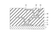
- FIG. 1 and 2 are enlarged cross-sectional views showing an example of the above-mentioned conventional multilayer wiring board.
- FIG. 1 shows circuit patterns of each layer (first metal wiring layer 21, second metal wiring layer 22, third metal wiring layer 23) and interlayer connection wiring (first via hole plating layer 61, second) using the same type of metal material. It is an enlarged sectional view of the multilayer wiring board which formed the via hole plating layer 62).
- FIG. 2 shows an enlarged cross-sectional view of a multilayer wiring board made of two or more types of metal materials. 1 and 2 show a multilayer wiring board in which three conductive layers are formed on one side.
- the electrical connection between the conductive layers of FIGS. 1 and 2 is formed by forming via holes 41 and 42 reaching the target conductive layer by ablating the insulating layer 3 by, for example, photolithography technology or laser light, and the via holes 41, This is done by forming beer hole plating layers 61 and 62 that are simultaneously applied at the time of pattern formation on the wall surface of 42.
- the first metal wiring layer 21, the second metal wiring layer 22, and the third metal wiring layer 23 are electrically connected via the via hole plating layers 61 and 62. ..
- a seed layer serving as a feeding layer for plating is required.
- a metal material of the same type as the wiring material is used for the seed layer
- a different material different from the wiring material is used for the seed layer.
- a metal different from the wiring material (first dissimilar metal layer 51, second dissimilar metal layer 52) is formed on the seed layer of electroplating as shown in FIG. 2 by a dry process such as sputtering coating to form the wiring layer.
- the process of formation has become commonplace.
- the wiring layer at the bottom of the via holes 41 and 42 has a structure separated by dissimilar metal layers 51 and 52.
- the via hole diameter (opening cross section) is reduced due to a request for miniaturization of the size, and the wiring connection area at the bottom of the via hole is reduced.
- the thermal stress caused by the difference in the coefficient of thermal expansion between the insulating layer and the metal wiring layer in the illustrated example of FIG. 2, the interface between the dissimilar metal layer 51 and the first metal wiring layer 21 at the bottom of the via hole and the dissimilar metal layer 52 Cracks or breaks may occur at the interface of the second metal wiring layer 22. Therefore, in the configuration as shown in FIG. 2, it is required to improve the connection reliability of the via connection.
- Patent Document 1 describes a multilayer wiring board having a through hole filled with one or more low elastic modulus fillers around a via hole for electrically connecting metal wiring layers sandwiching an insulating layer, and a method for manufacturing the same. It is disclosed.
- Patent Document 2 discloses a multilayer wiring board that forms one or more dummy via holes that are not connected to a circuit pattern around the via holes, and a method for manufacturing the same.
- Patent Document 1 and Patent Document 2 there is a problem that a through hole or a non-through hole that is not involved in the electrical connection must be formed, which complicates the process.
- the present invention has been made by paying attention to the above problems, and an object of the present invention is to improve the connection reliability of the via hole connection portion more easily.
- a plurality of metal wiring layers sequentially laminated via an insulating layer are electrically connected via a via hole plating layer formed along the surface of the via hole.
- a dissimilar metal layer made of a material different from the metal wiring layer is interposed between the metal wiring layer on the bottom surface side of the via hole and the metal wiring layer on the bottom surface side of the via hole.
- a recess is formed at a position in the wiring layer where the dissimilar metal layers come into contact, and the dissimilar metal layer is arranged in a concave shape along the surface of the recess formed in the metal wiring layer on the bottom surface side of the via hole.
- FIG. 5 is an enlarged cross-sectional view of a multilayer wiring board formed of two or more types of metal materials in a conventional example. It is a partially enlarged sectional view which shows an example of the multilayer wiring board which concerns on embodiment based on this invention. It is a partially enlarged sectional view explaining the via hole bottom part of the multilayer wiring board which concerns on embodiment based on this invention. It is a partially enlarged sectional view explaining the via hole bottom part of the multilayer wiring board which concerns on embodiment based on this invention.
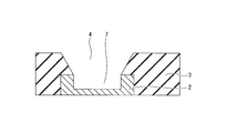
- FIG. 3 is a partially enlarged cross-sectional view showing an example of the multilayer wiring board of the present embodiment.
- the beer hall illustrates the case of a conformal via.
- the present invention can also be implemented in a beer hall filled via. The same parts as those of the conventional structure described above will be described with the same reference numerals.
- the core substrate 1 is formed by forming an insulating material such as glass epoxy resin, glass, or ceramic in a plate shape.
- an insulating material such as glass epoxy resin, glass, or ceramic
- FIG. 3 a multilayer wiring board in which three conductive layers (metal wiring layers) are formed on one side (upper surface in FIG. 1) of the core substrate 1 is shown.
- the structure is such that a first metal wiring layer made of copper, for example, a second metal wiring layer, and a third metal wiring layer are laminated on the core substrate 1 in this order via an insulating layer.
- FIG. 3 shows the one with the core substrate 1, the multilayer wiring board of the present invention can also be applied to the one without the core substrate and the wiring layer laminated on the interposer.
- the method for producing the first metal wiring layer 21 is not particularly limited, but it is desirable because it is easy to form by the semi-additive method and a substrate having a high wiring density can be produced.
- a first seed layer is formed on the core substrate 1 by sputter coating of Ti and Cu, electroless Ni plating, Cu plating, etc., and a photoresist layer is formed on the first seed layer.
- the photoresist may be a positive or negative liquid resist or a dry film resist.
- the photoresist is preferably a dry film resist, which is convenient, inexpensive, and desirable.
- a photomask on which a desired wiring pattern is drawn or a desired pattern is exposed using a direct drawing apparatus that directly draws the resist layer to form a first plating resist pattern.
- electrolytic copper plating is performed, the unnecessary first plating resist pattern is peeled off, and the unnecessary first seed layer is etched to form the first metal wiring layer 21.
- the insulating layer 3 is formed on the first metal wiring layer 21.
- the insulating layer 3 is made of a resin material such as a photosensitive polyimide resin, a photosensitive polybenzoxazole resin, a polyimide resin, an epoxy resin, a bismaleimide triazine resin, a cyanate resin, a polyphenylene oxide, a liquid crystal polymer, or a silicone resin, or a composite material thereof. It is formed. It is desirable to use a photosensitive polyimide resin or a photosensitive polybenzoxazole resin because it is easy to form a fine pattern and has excellent heat resistance and electrical characteristics.
- the thickness of the insulating layer 3 is not particularly limited, but is preferably 0.5 ⁇ m or more and 30 ⁇ m or less. If the thickness of the insulating layer 3 is smaller than 0.5 ⁇ m, there is a concern that the insulation reliability between the metal wiring layers may decrease. On the other hand, when the thickness of the insulating layer 3 is larger than 30 ⁇ m, it is disadvantageous for forming a fine circuit.
- a method for forming the insulating layer 3 if it is in the form of a sheet, it can be formed on the core substrate 1 by a roll laminating method, a vacuum laminating method, or the like.
- the liquid varnish can be formed by a known method such as a spin coating method, a die coating method, a curtain coating method, or a roller coating method.
- a via hole 41 for electrically connecting the first metal wiring layer 21 and the second metal wiring layer 22 is formed.
- the via hole 41 is formed by a photolithography technique or by ablating the insulating layer 3 with a laser beam.
- the via hole diameter is not particularly limited, but is preferably 2 ⁇ m or more and 100 ⁇ m or less. If the via hole diameter is smaller than 2 ⁇ m, there is a concern that the via connection reliability may decrease. On the other hand, if the via hole diameter is larger than 100 ⁇ m, it is disadvantageous for forming a fine circuit.
- the metal wiring pattern exposed on the bottom surface side of the via hole is etched to form the recess 7 as shown in FIG. 4 or 7 on the upper surface of the first metal wiring layer 21.
- the above etching is preferably performed by dry etching, and it is desirable to perform dry etching with an ion gun or Ar plasma because the recesses can be formed with good yield. It is desirable that the recess 7 formed in the first metal wiring layer 21 be etched perpendicularly to the core substrate 1.
- the angle of the wall surface of the recess 7 is the angle formed by the wall surface of the metal wiring layer recess 7 on the bottom surface side of the via hole with respect to the metal wiring-insulating layer interface (synonymous with the upper surface of the core substrate 1) as shown in the angle A1 of FIG. ,
- angles A1 and A2 are smaller than 75 degrees, the force applied in the horizontal direction of the wiring board cannot be suppressed when the insulating layer is thermally expanded and contracted, and the effect of preventing the via hole plating layer and the metal wiring layer on the bottom surface side of the via hole from peeling off is effective. There is a concern that it will become smaller.
- the angles A1 and A2 are larger than 105 degrees, there is a concern that the dissimilar metal layer formed in the next step is not continuously formed on the concave wall surface. It is preferable that the angles A1 and A2 are closer to 90 degrees in the side view than the inclination angle along the axial direction of the wall surface of the via hole.
- the depth of the recess 7 formed at the bottom of the via hole by the above dry etching is about 10 mm or more and 500 nm or less. If the depth of the recess is smaller than 10 nm, the depth embedded in the metal wiring layer on the bottom surface of the via hole becomes small, and there is a concern that the effect of preventing the via hole plating layer and the metal wiring layer on the bottom surface of the via hole from peeling off becomes small. .. On the other hand, when the recess is larger than 500 nm, the amount of dry etching is large, and it becomes difficult to form the recess with good yield. The depth of the recess is more preferably 50 nm or more and 500 nm or less.
- FIG. 4 is a partially enlarged cross-sectional view illustrating the bottom of the via hole of the multilayer wiring board of the present embodiment.
- a metal wiring pattern composed of a metal wiring layer exposed on the bottom surface side of the via hole, as shown in FIG.
- the upper end of the is directly continuous, and there is no step between the two.
- the opening on the bottom surface of the via hole and the opening of the recess 7 formed in the metal wiring layer on the bottom surface side of the via hole have the same diameter and shape.
- the dissimilar metal layer 5 is formed along the wall surface of the via hole as shown in FIG. 4 and the bottom surface and the wall surface of the recess 7, the result is as shown in FIG.
- FIG. 7 is a partially enlarged cross-sectional view illustrating another via hole bottom portion of the multilayer wiring board of the present embodiment.
- the area of the opening on the bottom surface of the via hole may be larger than the cross-sectional area of the opening of the recess 7 formed on the upper surface of the metal wiring layer on the bottom surface side of the via hole.
- the width of the recess 7 may be designed to be smaller than the diameter on the bottom surface side of the via hole.
- the bottom end of the beer hole wall surface is arranged outside the upper end of the wall surface of the recess 7 formed in the metal wiring layer, and the bottom end of the via hole wall surface and the upper end of the wall surface of the recess 7 are arranged.
- the space is indirectly connected via the upper surface of the metal wiring layer.
- the dissimilar metal layer 5 is likely to be uniformly formed on the wall surface of the via hole 4 and the recess 7 on the bottom surface side of the via hole.
- a treatment such as immersing the via hole in which the recess 7 is formed in oxygen plasma or an etching solution to etch the insulating layer 3 on the wall surface of the via hole.
- the opening diameter of the recess formed in the metal wiring pattern on the bottom surface of the via hole with respect to the opening diameter of the bottom surface of the via hole is preferably 50% or more and 100% or less.
- the ratio of the opening diameters is not 50% or more and 100% or less, there is a concern that it becomes difficult to form a dissimilar metal layer in the recess.
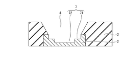
- FIG. 10 is a partially enlarged cross-sectional view illustrating the bottom of another via hole of the multilayer wiring board of the present embodiment.
- the example shown in FIG. 10 is an example in which the recess 7 has a multi-stage structure in which the opening cross-sectional area of the recess gradually increases from the bottom surface of the recess toward the upper via hole side. That is, the recess 7 may have a multi-stage structure in which the opening width is narrowed stepwise toward the bottom (bottom side).
- the metal wiring layer 2 on the bottom surface side of the via hole may be formed with a recess shape including an upper recess first portion 71 and a lower recess second portion 72 as recesses.
- the wall surface of the recessed portion 1 71 has a structure continuous with the wall surface of the via hole 4, and the recessed portion 2 72 is formed in the recessed portion 1 71.
- the dissimilar metal layer 5 can be easily formed uniformly by the via hole wall surface and the via hole bottom surface side recess 7. Further, since the ground contact area between the metal wiring layer 2 and the dissimilar metal layer 5 on the bottom surface side of the via hole becomes large, the via connection reliability can be improved.
- a method such as forming an etching resist pattern so as to etch only a desired portion after forming the via hole can be considered.
- the ratio of the opening diameter of the recessed portion 72 to the recessed portion 1 71 is preferably 50% or more and 100% or less. If the ratio of the opening diameters is not 50% or more and 100% or less, there is a concern that it becomes difficult to form a dissimilar metal layer in the recess 7.
- the recessed portion 2 72 is vertically etched, and the metal wiring layer parallel to the wall surface of the recessed portion 2 72 of the metal wiring layer on the bottom surface side of the via hole and the upper surface of the core substrate as shown at the angle A3 in FIG. It is desirable that the angle formed by the etching is 75 degrees or more and 105 degrees or less.
- the angle of A3 is smaller than 75 degrees, the force applied in the horizontal direction of the wiring board cannot be suppressed when the insulating layer is thermally expanded and contracted, and the effect of preventing the via hole plating layer and the metal wiring layer on the bottom surface side of the via hole from peeling off is small. There is a concern.
- the angle of A3 is larger than 105 degrees, there is a concern that the dissimilar metal layer formed in the next step is not continuously formed on the wall surface of the second recess.
- the depth of the recessed part 2 72 is preferably about 10 nm or more and 500 nm or less.
- the depth of the recessed second portion 72 is smaller than 10 nm, the depth embedded in the metal wiring layer 2 on the bottom surface side of the via hole becomes shallow, and the effect of preventing the via hole plating layer 61 and the metal wiring layer 2 on the bottom surface side of the via hole from peeling off.
- the concave portion 2 portion 72 is larger than 500 nm, the amount of dry etching is large, and it becomes difficult to form the concave portion 2 portion 72 with good yield.
- the depth of the recess portion 2 72 is more preferably 50 nm or more and 500 nm or less.
- a dissimilar metal layer 51 is formed on the bottom surface and inner wall surface of the via hole in which the recess 7 is formed, and the surface of the insulating layer.
- the dissimilar metal layer may be Ti, Ni, Ag, Sn, Au or the like, but Ti is desirable because it has high strength and is difficult to expand and contract with heat.
- Examples of the method for forming the dissimilar metal layer 5 include a sputtering method, a CVD method, a vapor deposition method, an ion plating method, an electroless plating method, and the like, but the sputtering method is simple and realistic.
- the concave dissimilar metal layer is formed so as to be embedded in the metal wiring layer 2 on the bottom surface side of the via hole.
- the via hole plating layer 61 and the second metal wiring layer 22 are produced.
- the method for producing the via hole plating layer 61 and the second metal wiring layer 22 is not particularly limited, but it is desirable because it is easy to form by the semi-additive method and a substrate having a high wiring density can be produced.
- An example of the manufacturing method will be described.
- the formed dissimilar metal layer 51 is used as a seed layer, and a photoresist layer is formed on the dissimilar metal layer.
- the plating resist pattern is formed by exposure using a photomask on which the desired wiring pattern is drawn or a direct drawing device that directly draws the desired pattern.
- the plating resist pattern After forming the plating resist pattern, electrolytic copper plating is performed, the unnecessary plating resist pattern is peeled off, and the dissimilar metal layer 51 on which the wiring pattern is not formed on the unnecessary upper part is removed by etching. As a result, the via hole plating layer 61 and the second metal wiring layer 22 are formed.
- the insulating layer 3 is formed, and then the via hole 42 for electrically connecting the second metal wiring layer 22 and the third metal wiring layer 23 is formed. Further, oxygen plasma treatment is applied to the insulating layer 3 on which the via hole 42 is formed, smear on the bottom surface of the via hole and the surface of the insulating layer are roughened, and then the metal wiring pattern exposed on the bottom surface side of the via hole is etched to obtain a second metal. A recess is formed in the wiring layer 22. A dissimilar metal layer 52 is formed on the bottom surface and inner wall surface of the via hole in which the recess is formed, and the surface of the insulating layer to produce the via hole plating layer 62 and the third metal wiring layer 23.
- a photoresist layer is formed on the dissimilar metal layer, and a photomask on which a desired wiring pattern is drawn or a direct drawing apparatus for directly drawing a desired pattern is used. It is exposed to form a plating resist pattern.
- electrolytic copper plating is performed to peel off the unnecessary plating resist pattern, and the dissimilar metal layer 52 in which the wiring pattern is not formed on the unnecessary upper part is removed by etching. As a result, the via hole plating layer 62 and the third metal wiring layer 23 are formed.
- the via hole plating layer formed on the inner wall surface of the via hole 4 is also formed in the horizontal direction of the multi-layer wiring board. Thermal stress is applied due to the thermal expansion and contraction of the plating layer, and a load for breaking the plating layer is applied.
- the via hole plating layer is formed on the dissimilar metal layer 5, and the dissimilar metal layer 5 is embedded in the metal wiring layer 2 on the bottom surface side of the via hole.
- the layer and the metal wiring layer on the bottom surface side of the via hole mesh with each other with the dissimilar metal layer sandwiched between them, and as a result, the peeling of the via hole plating layer and the metal wiring joint portion at the bottom can be prevented. Therefore, in this embodiment, the connection reliability between the metal wiring layers can be improved.
- the multilayer wiring board of the present embodiment the following excellent effects can be exhibited.
- the above A dissimilar metal layer made of a material different from the metal wiring layer is interposed between the metal wiring layer on the bottom surface side of the via hole and the metal wiring layer on the bottom surface side of the via hole.
- a recess is formed at a position where the two are in contact with each other, and the dissimilar metal layer is arranged in a concave shape along the surface of the recess formed in the metal wiring layer on the bottom surface side of the via hole.
- the thickness of the dissimilar metal layer is preferably 5 nm or more and 100 nm or less. Further, the depth of the recess is preferably 10 nm or more and 500 nm or less. Further, the angle of the wall surface of the recess with respect to the surface of the substrate on which the metal wiring layer is formed is preferably 75 degrees or more and 105 degrees or less. In the present embodiment, at least a part of the dissimilar metal layer is arranged along the surface of the via hole, and the dissimilar metal layer arranged along the recess is a dissimilar metal formed along the wall surface of the via hole. It may be configured to be electrically connected to the layer.
- the bottom end of the wall surface of the via hole formed in the insulating layer may be directly continuous with the upper end of the recess.
- the opening on the bottom side of the via hole formed in the insulating layer is formed wider than the opening of the recess, and is arranged along the dissimilar metal layer arranged along the recess and the wall surface of the via hole.
- the dissimilar metal layer may be electrically connected via a dissimilar metal layer formed along the upper surface of the metal wiring layer on the bottom surface side of the via hole.
- the recess may have a multi-stage structure in which the opening cross-sectional area of the recess gradually increases from the bottom surface of the recess toward the via hole side.
- the multi-stage structure is a two-stage structure.
- the metal wiring layer and the via hole plating layer may each contain copper as a material.
- the dissimilar metal layer may be configured to contain titanium as a material.
- the dissimilar metal layer may have a structure in which nickel is contained in the material.
- the above-mentioned multilayer wiring board is manufactured, for example, as follows. That is, in the present embodiment, a step of forming a first seed layer on the main surface which is the surface of the core substrate by sputtering, a step of forming a first plating resist pattern on the first seed layer, and a step of electrolytic plating are performed. A step of forming a 1-metal wiring layer, a step of peeling off a first resist pattern formed on the first seed layer, a step of etching a first seed layer other than the first metal wiring layer, and a step of forming a first metal.
- the gist is to include a step of forming a pattern and a step of peeling off a second plating resist layer that is no longer needed after forming the pattern of the second metal wiring layer, and etching and removing the second seed layer of the unnecessary portion. Adopt the manufacturing method of the multilayer wiring board.
- a step of forming a first seed layer on the main surface, which is the surface of the core substrate, by sputtering, a step of forming a first plating resist pattern on the first seed layer, and a step of electrolytic plating a step of forming a 1-metal wiring layer, a step of peeling off a first resist pattern formed on the first seed layer, a step of etching a first seed layer other than the first metal wiring layer, and a step of forming a first metal.
- the process the step of performing oxygen plasma treatment on the exposed upper part of the first metal wiring layer to clean the opening, and the step of performing reverse sputtering treatment on the cleaned opening to etch the first metal wiring layer of the opening.
- the gist is to include a step of forming a pattern and a step of peeling off a second plating resist layer that is no longer needed after forming the pattern of the second metal wiring layer, and etching and removing the second seed layer of the unnecessary portion. Adopt the manufacturing method of the multilayer wiring board.
- first seed layers 8 and 8A are formed on both sides of the core substrate 1.
- the formation of the first seed layer was carried out using a sputtering apparatus, which is a film forming apparatus utilizing the phenomenon that the solid material pops out from the solid surface by colliding the ionized and accelerated atoms or molecules with the surface of the material.
- a Cu film as the first seed layers 8 and 8A was formed on the core substrate 1 to a thickness of 300 nm.
- the first plating resist patterns 9 and 9A are formed on the first seed layers 8 and 8A.
- the resist was laminated with a 25 ⁇ m-thick dry film resist, exposed using a photomask on which a pattern corresponding to the wiring circuit was drawn, and then spray-developed with a 1% sodium carbonate aqueous solution.
- the first plating resist patterns 9 and 9A were produced on the core substrate 1.
- electrolytic copper plating having a thickness of 1 ⁇ m was performed using the first seed layer as a feeding layer, and the unnecessary first plating resist pattern was made into a 3% sodium hydroxide solution at 60 ° C.
- the first metal wiring layers 21 and 21A were formed by performing a spray peeling treatment and further removing the first seed layer of the unnecessary portion with a sulfuric acid-hydrogen peroxide solution.
- insulating layers 3 and 3A and via holes 4 and 4A were formed.
- the wiring substrate on which the first metal wiring layers 21 and 21A are formed is immersed in a solution of 10% sulfuric acid for cleaning, and then HD-4104 (manufactured by Hitachi Chemical DuPont Microsystems) is coated by a spin coating method.
- HD-4104 manufactured by Hitachi Chemical DuPont Microsystems
- the parts other than the parts corresponding to the via holes 4 and 4A are directly exposed using a drawing device, organically developed, and then cured to form the insulating layers 3 and 3A having a thickness of 5 ⁇ m and the via holes 4 and 4A. did.
- oxygen plasma treatment was performed to roughen the smear at the bottom of the via holes 4 and 4A and the surface of the insulating layer.
- the first metal wiring exposed from the bottom of the via hole was subjected to argon ion gun treatment (dry etching treatment) 10 and 10A on the front and back of the wiring board after the oxygen plasma treatment.
- Recesses 7 and 7A were formed in the layers 21 and 21A.
- via holes 4 and 4A having recesses 7 and 7A formed at the bottom and dissimilar metal layers 5 and 5A were formed on the surface of the insulating layer.
- a Ti film of 50 nm was formed as the dissimilar metal layers 5 and 5A using a sputtering device, and the dissimilar metal layers 5 and 5A were used as seed layers for electrolytic copper plating. In this way, a part of the dissimilar metal layers 5 and 5A was embedded in the first metal wiring layers 21 and 21A at the bottom of the via hole.
- a 25 ⁇ m-thick dry film resist is laminated on the dissimilar metal layer 5, and exposure treatment is performed using a photomask on which a pattern corresponding to the wiring circuit is drawn, and then 1%.
- the second plating resist patterns 11 and 11A were formed by performing a spray development treatment with an aqueous solution of sodium carbonate.
- a 15 ⁇ m-thick electrolytic copper plating was performed on the wiring substrate on which the second plating resist pattern was formed, using dissimilar metal layers 5 and 5A as a feeding layer, and the second plating became unnecessary. By spray-peeling the resist pattern into a 3% sodium hydroxide solution at 60 ° C.
- the second metal wiring layers 22 and 22A are simultaneously removed at the same time.
- the via hole plating layers 6 and 6A were formed inside the via hole in which the recess was formed.
- the present invention is not limited to the examples described above and shown in the drawings, and various modifications can be carried out within a range not deviating from the gist thereof.
- the case where the multi-layer wiring board of the embodiment has four metal wiring layers has been described, but it can also be widely applied to a further multi-layer wiring board having six or eight metal wiring layers.
- the scope of the present invention is not limited to the exemplary embodiments illustrated and described, but also includes all embodiments that provide an effect equal to that intended by the present invention. Furthermore, the scope of the present invention is not limited to the combination of the features of the invention defined by the claims, but may be defined by any desired combination of the specific features of all the disclosed features. In addition, the entire contents of Japanese Patent Application No. 2019-102736 (filed on May 31, 2019), for which the present application claims priority, form a part of the present disclosure by reference.
Landscapes
- Engineering & Computer Science (AREA)
- Microelectronics & Electronic Packaging (AREA)
- Manufacturing & Machinery (AREA)
- Production Of Multi-Layered Print Wiring Board (AREA)
Priority Applications (4)
| Application Number | Priority Date | Filing Date | Title |
|---|---|---|---|
| CN202080040000.8A CN113994770B (zh) | 2019-05-31 | 2020-05-26 | 多层配线基板及其制造方法 |
| JP2021522787A JPWO2020241645A1 (https=) | 2019-05-31 | 2020-05-26 | |
| EP20815677.8A EP3979774A4 (en) | 2019-05-31 | 2020-05-26 | MULTILAYER CIRCUIT BOARD AND METHOD OF MANUFACTURE THEREOF |
| US17/534,936 US11917751B2 (en) | 2019-05-31 | 2021-11-24 | Multilayer wiring board and method of producing the same |
Applications Claiming Priority (2)
| Application Number | Priority Date | Filing Date | Title |
|---|---|---|---|
| JP2019102736 | 2019-05-31 | ||
| JP2019-102736 | 2019-05-31 |
Related Child Applications (1)
| Application Number | Title | Priority Date | Filing Date |
|---|---|---|---|
| US17/534,936 Continuation US11917751B2 (en) | 2019-05-31 | 2021-11-24 | Multilayer wiring board and method of producing the same |
Publications (1)
| Publication Number | Publication Date |
|---|---|
| WO2020241645A1 true WO2020241645A1 (ja) | 2020-12-03 |
Family
ID=73553763
Family Applications (1)
| Application Number | Title | Priority Date | Filing Date |
|---|---|---|---|
| PCT/JP2020/020760 Ceased WO2020241645A1 (ja) | 2019-05-31 | 2020-05-26 | 多層配線基板及びその製造方法 |
Country Status (5)
| Country | Link |
|---|---|
| US (1) | US11917751B2 (https=) |
| EP (1) | EP3979774A4 (https=) |
| JP (1) | JPWO2020241645A1 (https=) |
| CN (1) | CN113994770B (https=) |
| WO (1) | WO2020241645A1 (https=) |
Cited By (1)
| Publication number | Priority date | Publication date | Assignee | Title |
|---|---|---|---|---|
| TWI901331B (zh) * | 2021-08-06 | 2025-10-11 | 群創光電股份有限公司 | 封裝元件的製作方法 |
Families Citing this family (2)
| Publication number | Priority date | Publication date | Assignee | Title |
|---|---|---|---|---|
| JP2024006576A (ja) * | 2022-07-04 | 2024-01-17 | 新光電気工業株式会社 | 配線基板及びその製造方法 |
| CN117279218B (zh) * | 2023-10-16 | 2024-05-24 | 江苏皓越真空设备有限公司 | 一种多层覆铜陶瓷基板的制备方法 |
Citations (6)
| Publication number | Priority date | Publication date | Assignee | Title |
|---|---|---|---|---|
| JP2009295850A (ja) * | 2008-06-06 | 2009-12-17 | Hitachi Chem Co Ltd | 多層回路基板の製造方法及びこれから得られる多層回路基板、半導体チップ搭載基板並びにこの基板を用いた半導体パッケージ |
| JP2010205801A (ja) * | 2009-02-27 | 2010-09-16 | Kyocer Slc Technologies Corp | 配線基板の製造方法 |
| JP2012094734A (ja) * | 2010-10-28 | 2012-05-17 | Shinko Electric Ind Co Ltd | 配線基板及びその製造方法 |
| JP2017098422A (ja) * | 2015-11-25 | 2017-06-01 | 新光電気工業株式会社 | 配線基板及び配線基板の製造方法 |
| JP2017157758A (ja) * | 2016-03-03 | 2017-09-07 | ウシオ電機株式会社 | 配線基板の製造方法および配線基板 |
| JP2019102736A (ja) | 2017-12-06 | 2019-06-24 | 實野 孝久 | 半導体パッケージ及び半導体チップのチップidマーキング方法 |
Family Cites Families (17)
| Publication number | Priority date | Publication date | Assignee | Title |
|---|---|---|---|---|
| US6674017B1 (en) * | 1998-12-24 | 2004-01-06 | Ngk Spark Plug Co., Ltd. | Multilayer-wiring substrate and method for fabricating same |
| JP3925100B2 (ja) | 2001-04-18 | 2007-06-06 | 凸版印刷株式会社 | 多層プリント基板 |
| JP2002319767A (ja) | 2001-04-23 | 2002-10-31 | Toppan Printing Co Ltd | 多層プリント基板 |
| JP2006032476A (ja) * | 2004-07-13 | 2006-02-02 | Fujikura Ltd | ビアフィリングめっき方法 |
| US7190078B2 (en) * | 2004-12-27 | 2007-03-13 | Khandekar Viren V | Interlocking via for package via integrity |
| US8264086B2 (en) * | 2005-12-05 | 2012-09-11 | Taiwan Semiconductor Manufacturing Company, Ltd. | Via structure with improved reliability |
| JP2009038080A (ja) * | 2007-07-31 | 2009-02-19 | Panasonic Corp | 半導体装置及びその製造方法 |
| JP2010199318A (ja) * | 2009-02-25 | 2010-09-09 | Kyocera Corp | 配線基板及びそれを備えた実装構造体 |
| JP5479233B2 (ja) * | 2010-06-04 | 2014-04-23 | 新光電気工業株式会社 | 配線基板及びその製造方法 |
| CN102693962A (zh) * | 2011-03-22 | 2012-09-26 | 精材科技股份有限公司 | 具有电磁屏蔽作用的集成电路晶圆及其制造方法 |
| JP5540276B2 (ja) * | 2011-03-31 | 2014-07-02 | Tdk株式会社 | 電子部品内蔵基板及びその製造方法 |
| JP6241641B2 (ja) * | 2013-03-28 | 2017-12-06 | 日立化成株式会社 | 多層配線基板の製造方法 |
| KR101506785B1 (ko) * | 2013-05-29 | 2015-03-27 | 삼성전기주식회사 | 인쇄회로기판 |
| JP6350062B2 (ja) * | 2013-10-09 | 2018-07-04 | 日立化成株式会社 | 多層配線基板の製造方法 |
| JP2015162660A (ja) * | 2014-02-28 | 2015-09-07 | イビデン株式会社 | プリント配線板、プリント配線板の製造方法、パッケージ−オン−パッケージ |
| JP6324876B2 (ja) * | 2014-07-16 | 2018-05-16 | 新光電気工業株式会社 | 配線基板、半導体装置及び配線基板の製造方法 |
| KR102107035B1 (ko) * | 2014-11-10 | 2020-05-07 | 삼성전기주식회사 | 인쇄회로기판 및 그 제조방법 |
-
2020
- 2020-05-26 JP JP2021522787A patent/JPWO2020241645A1/ja active Pending
- 2020-05-26 EP EP20815677.8A patent/EP3979774A4/en active Pending
- 2020-05-26 CN CN202080040000.8A patent/CN113994770B/zh active Active
- 2020-05-26 WO PCT/JP2020/020760 patent/WO2020241645A1/ja not_active Ceased
-
2021
- 2021-11-24 US US17/534,936 patent/US11917751B2/en active Active
Patent Citations (6)
| Publication number | Priority date | Publication date | Assignee | Title |
|---|---|---|---|---|
| JP2009295850A (ja) * | 2008-06-06 | 2009-12-17 | Hitachi Chem Co Ltd | 多層回路基板の製造方法及びこれから得られる多層回路基板、半導体チップ搭載基板並びにこの基板を用いた半導体パッケージ |
| JP2010205801A (ja) * | 2009-02-27 | 2010-09-16 | Kyocer Slc Technologies Corp | 配線基板の製造方法 |
| JP2012094734A (ja) * | 2010-10-28 | 2012-05-17 | Shinko Electric Ind Co Ltd | 配線基板及びその製造方法 |
| JP2017098422A (ja) * | 2015-11-25 | 2017-06-01 | 新光電気工業株式会社 | 配線基板及び配線基板の製造方法 |
| JP2017157758A (ja) * | 2016-03-03 | 2017-09-07 | ウシオ電機株式会社 | 配線基板の製造方法および配線基板 |
| JP2019102736A (ja) | 2017-12-06 | 2019-06-24 | 實野 孝久 | 半導体パッケージ及び半導体チップのチップidマーキング方法 |
Cited By (1)
| Publication number | Priority date | Publication date | Assignee | Title |
|---|---|---|---|---|
| TWI901331B (zh) * | 2021-08-06 | 2025-10-11 | 群創光電股份有限公司 | 封裝元件的製作方法 |
Also Published As
| Publication number | Publication date |
|---|---|
| EP3979774A1 (en) | 2022-04-06 |
| US11917751B2 (en) | 2024-02-27 |
| CN113994770A (zh) | 2022-01-28 |
| EP3979774A4 (en) | 2022-07-27 |
| US20220087016A1 (en) | 2022-03-17 |
| JPWO2020241645A1 (https=) | 2020-12-03 |
| CN113994770B (zh) | 2024-09-10 |
Similar Documents
| Publication | Publication Date | Title |
|---|---|---|
| KR100295932B1 (ko) | 인쇄회로기판제조방법및이에의해형성된인쇄회로기판 | |
| US8052882B2 (en) | Method of manufacturing wiring substrate | |
| JPH09213567A (ja) | 薄膜コンデンサおよびその製造方法 | |
| US11917751B2 (en) | Multilayer wiring board and method of producing the same | |
| JP2018093061A (ja) | 電子部品及び電子部品製造方法 | |
| JP2007208263A (ja) | 薄膜キャパシタ内蔵型印刷回路基板の製造方法 | |
| CN103416110A (zh) | 印刷电路板及其制造方法 | |
| WO2017094470A1 (ja) | 多層プリント配線基板及びその製造方法 | |
| TWI403237B (zh) | 形成通過在高密度互連(hdi)基材材料上之介電塗層之固態盲孔之方法 | |
| CN103416109A (zh) | 印刷电路板及其制造方法 | |
| JP2006100631A (ja) | 配線基板及びその製造方法 | |
| US6574863B2 (en) | Thin core substrate for fabricating a build-up circuit board | |
| US6629366B1 (en) | Method of producing a multilayer wiring board | |
| JP2022147360A (ja) | 多層配線基板およびその製造方法 | |
| JP2008172151A (ja) | 多層配線基板 | |
| JP2018148086A (ja) | 貫通電極基板の製造方法及び貫通電極基板 | |
| TWI595811B (zh) | 印刷電路板及其製造方法 | |
| US8273256B2 (en) | Method for manufacturing wiring structure of wiring board | |
| KR100294157B1 (ko) | 다층인쇄회로기판의층간전기접속방법 | |
| TWI691245B (zh) | 線路板的製作方法 | |
| TWI691244B (zh) | 線路板結構 | |
| JP2013110408A (ja) | 印刷回路基板及びその製造方法 | |
| TWI327367B (en) | Semiconductor substrate structure and method for fabricating the same | |
| TWI223579B (en) | Patterned circuit layer of semiconductor package substrate and method for fabricating the same | |
| JP2002124765A (ja) | プリント配線板の製造方法 |
Legal Events
| Date | Code | Title | Description |
|---|---|---|---|
| 121 | Ep: the epo has been informed by wipo that ep was designated in this application |
Ref document number: 20815677 Country of ref document: EP Kind code of ref document: A1 |
|
| ENP | Entry into the national phase |
Ref document number: 2021522787 Country of ref document: JP Kind code of ref document: A |
|
| NENP | Non-entry into the national phase |
Ref country code: DE |
|
| ENP | Entry into the national phase |
Ref document number: 2020815677 Country of ref document: EP Effective date: 20220103 |