WO2020235205A1 - 炭化珪素基板 - Google Patents
炭化珪素基板 Download PDFInfo
- Publication number
- WO2020235205A1 WO2020235205A1 PCT/JP2020/012435 JP2020012435W WO2020235205A1 WO 2020235205 A1 WO2020235205 A1 WO 2020235205A1 JP 2020012435 W JP2020012435 W JP 2020012435W WO 2020235205 A1 WO2020235205 A1 WO 2020235205A1
- Authority
- WO
- WIPO (PCT)
- Prior art keywords
- silicon carbide
- main surface
- carbide substrate
- chamfered portion
- concentration
- Prior art date
- Legal status (The legal status is an assumption and is not a legal conclusion. Google has not performed a legal analysis and makes no representation as to the accuracy of the status listed.)
- Ceased
Links
Images




Classifications
-
- H—ELECTRICITY
- H10—SEMICONDUCTOR DEVICES; ELECTRIC SOLID-STATE DEVICES NOT OTHERWISE PROVIDED FOR
- H10P—GENERIC PROCESSES OR APPARATUS FOR THE MANUFACTURE OR TREATMENT OF DEVICES COVERED BY CLASS H10
- H10P70/00—Cleaning of wafers, substrates or parts of devices
- H10P70/10—Cleaning before device manufacture, i.e. Begin-Of-Line process
- H10P70/15—Cleaning before device manufacture, i.e. Begin-Of-Line process by wet cleaning only
-
- C—CHEMISTRY; METALLURGY
- C30—CRYSTAL GROWTH
- C30B—SINGLE-CRYSTAL GROWTH; UNIDIRECTIONAL SOLIDIFICATION OF EUTECTIC MATERIAL OR UNIDIRECTIONAL DEMIXING OF EUTECTOID MATERIAL; REFINING BY ZONE-MELTING OF MATERIAL; PRODUCTION OF A HOMOGENEOUS POLYCRYSTALLINE MATERIAL WITH DEFINED STRUCTURE; SINGLE CRYSTALS OR HOMOGENEOUS POLYCRYSTALLINE MATERIAL WITH DEFINED STRUCTURE; AFTER-TREATMENT OF SINGLE CRYSTALS OR A HOMOGENEOUS POLYCRYSTALLINE MATERIAL WITH DEFINED STRUCTURE; APPARATUS THEREFOR
- C30B29/00—Single crystals or homogeneous polycrystalline material with defined structure characterised by the material or by their shape
- C30B29/02—Elements
- C30B29/06—Silicon
-
- C—CHEMISTRY; METALLURGY
- C30—CRYSTAL GROWTH
- C30B—SINGLE-CRYSTAL GROWTH; UNIDIRECTIONAL SOLIDIFICATION OF EUTECTIC MATERIAL OR UNIDIRECTIONAL DEMIXING OF EUTECTOID MATERIAL; REFINING BY ZONE-MELTING OF MATERIAL; PRODUCTION OF A HOMOGENEOUS POLYCRYSTALLINE MATERIAL WITH DEFINED STRUCTURE; SINGLE CRYSTALS OR HOMOGENEOUS POLYCRYSTALLINE MATERIAL WITH DEFINED STRUCTURE; AFTER-TREATMENT OF SINGLE CRYSTALS OR A HOMOGENEOUS POLYCRYSTALLINE MATERIAL WITH DEFINED STRUCTURE; APPARATUS THEREFOR
- C30B29/00—Single crystals or homogeneous polycrystalline material with defined structure characterised by the material or by their shape
- C30B29/10—Inorganic compounds or compositions
- C30B29/36—Carbides
-
- C—CHEMISTRY; METALLURGY
- C30—CRYSTAL GROWTH
- C30B—SINGLE-CRYSTAL GROWTH; UNIDIRECTIONAL SOLIDIFICATION OF EUTECTIC MATERIAL OR UNIDIRECTIONAL DEMIXING OF EUTECTOID MATERIAL; REFINING BY ZONE-MELTING OF MATERIAL; PRODUCTION OF A HOMOGENEOUS POLYCRYSTALLINE MATERIAL WITH DEFINED STRUCTURE; SINGLE CRYSTALS OR HOMOGENEOUS POLYCRYSTALLINE MATERIAL WITH DEFINED STRUCTURE; AFTER-TREATMENT OF SINGLE CRYSTALS OR A HOMOGENEOUS POLYCRYSTALLINE MATERIAL WITH DEFINED STRUCTURE; APPARATUS THEREFOR
- C30B33/00—After-treatment of single crystals or homogeneous polycrystalline material with defined structure
-
- H—ELECTRICITY
- H10—SEMICONDUCTOR DEVICES; ELECTRIC SOLID-STATE DEVICES NOT OTHERWISE PROVIDED FOR
- H10D—INORGANIC ELECTRIC SEMICONDUCTOR DEVICES
- H10D62/00—Semiconductor bodies, or regions thereof, of devices having potential barriers
- H10D62/60—Impurity distributions or concentrations
-
- H—ELECTRICITY
- H10—SEMICONDUCTOR DEVICES; ELECTRIC SOLID-STATE DEVICES NOT OTHERWISE PROVIDED FOR
- H10D—INORGANIC ELECTRIC SEMICONDUCTOR DEVICES
- H10D62/00—Semiconductor bodies, or regions thereof, of devices having potential barriers
- H10D62/80—Semiconductor bodies, or regions thereof, of devices having potential barriers characterised by the materials
- H10D62/83—Semiconductor bodies, or regions thereof, of devices having potential barriers characterised by the materials being Group IV materials, e.g. B-doped Si or undoped Ge
- H10D62/832—Semiconductor bodies, or regions thereof, of devices having potential barriers characterised by the materials being Group IV materials, e.g. B-doped Si or undoped Ge being Group IV materials comprising two or more elements, e.g. SiGe
- H10D62/8325—Silicon carbide
-
- H—ELECTRICITY
- H10—SEMICONDUCTOR DEVICES; ELECTRIC SOLID-STATE DEVICES NOT OTHERWISE PROVIDED FOR
- H10P—GENERIC PROCESSES OR APPARATUS FOR THE MANUFACTURE OR TREATMENT OF DEVICES COVERED BY CLASS H10
- H10P90/00—Preparation of wafers not covered by a single main group of this subclass, e.g. wafer reinforcement
- H10P90/12—Preparing bulk and homogeneous wafers
- H10P90/128—Preparing bulk and homogeneous wafers by edge treatment, e.g. chamfering
-
- H—ELECTRICITY
- H10—SEMICONDUCTOR DEVICES; ELECTRIC SOLID-STATE DEVICES NOT OTHERWISE PROVIDED FOR
- H10P—GENERIC PROCESSES OR APPARATUS FOR THE MANUFACTURE OR TREATMENT OF DEVICES COVERED BY CLASS H10
- H10P90/00—Preparation of wafers not covered by a single main group of this subclass, e.g. wafer reinforcement
- H10P90/12—Preparing bulk and homogeneous wafers
- H10P90/129—Preparing bulk and homogeneous wafers by polishing
-
- C—CHEMISTRY; METALLURGY
- C09—DYES; PAINTS; POLISHES; NATURAL RESINS; ADHESIVES; COMPOSITIONS NOT OTHERWISE PROVIDED FOR; APPLICATIONS OF MATERIALS NOT OTHERWISE PROVIDED FOR
- C09G—POLISHING COMPOSITIONS; SKI WAXES
- C09G1/00—Polishing compositions
- C09G1/02—Polishing compositions containing abrasives or grinding agents
-
- C—CHEMISTRY; METALLURGY
- C09—DYES; PAINTS; POLISHES; NATURAL RESINS; ADHESIVES; COMPOSITIONS NOT OTHERWISE PROVIDED FOR; APPLICATIONS OF MATERIALS NOT OTHERWISE PROVIDED FOR
- C09G—POLISHING COMPOSITIONS; SKI WAXES
- C09G1/00—Polishing compositions
- C09G1/04—Aqueous dispersions
-
- C—CHEMISTRY; METALLURGY
- C30—CRYSTAL GROWTH
- C30B—SINGLE-CRYSTAL GROWTH; UNIDIRECTIONAL SOLIDIFICATION OF EUTECTIC MATERIAL OR UNIDIRECTIONAL DEMIXING OF EUTECTOID MATERIAL; REFINING BY ZONE-MELTING OF MATERIAL; PRODUCTION OF A HOMOGENEOUS POLYCRYSTALLINE MATERIAL WITH DEFINED STRUCTURE; SINGLE CRYSTALS OR HOMOGENEOUS POLYCRYSTALLINE MATERIAL WITH DEFINED STRUCTURE; AFTER-TREATMENT OF SINGLE CRYSTALS OR A HOMOGENEOUS POLYCRYSTALLINE MATERIAL WITH DEFINED STRUCTURE; APPARATUS THEREFOR
- C30B23/00—Single-crystal growth by condensing evaporated or sublimed materials
-
- C—CHEMISTRY; METALLURGY
- C30—CRYSTAL GROWTH
- C30B—SINGLE-CRYSTAL GROWTH; UNIDIRECTIONAL SOLIDIFICATION OF EUTECTIC MATERIAL OR UNIDIRECTIONAL DEMIXING OF EUTECTOID MATERIAL; REFINING BY ZONE-MELTING OF MATERIAL; PRODUCTION OF A HOMOGENEOUS POLYCRYSTALLINE MATERIAL WITH DEFINED STRUCTURE; SINGLE CRYSTALS OR HOMOGENEOUS POLYCRYSTALLINE MATERIAL WITH DEFINED STRUCTURE; AFTER-TREATMENT OF SINGLE CRYSTALS OR A HOMOGENEOUS POLYCRYSTALLINE MATERIAL WITH DEFINED STRUCTURE; APPARATUS THEREFOR
- C30B23/00—Single-crystal growth by condensing evaporated or sublimed materials
- C30B23/02—Epitaxial-layer growth
-
- C—CHEMISTRY; METALLURGY
- C30—CRYSTAL GROWTH
- C30B—SINGLE-CRYSTAL GROWTH; UNIDIRECTIONAL SOLIDIFICATION OF EUTECTIC MATERIAL OR UNIDIRECTIONAL DEMIXING OF EUTECTOID MATERIAL; REFINING BY ZONE-MELTING OF MATERIAL; PRODUCTION OF A HOMOGENEOUS POLYCRYSTALLINE MATERIAL WITH DEFINED STRUCTURE; SINGLE CRYSTALS OR HOMOGENEOUS POLYCRYSTALLINE MATERIAL WITH DEFINED STRUCTURE; AFTER-TREATMENT OF SINGLE CRYSTALS OR A HOMOGENEOUS POLYCRYSTALLINE MATERIAL WITH DEFINED STRUCTURE; APPARATUS THEREFOR
- C30B23/00—Single-crystal growth by condensing evaporated or sublimed materials
- C30B23/02—Epitaxial-layer growth
- C30B23/025—Epitaxial-layer growth characterised by the substrate
-
- C—CHEMISTRY; METALLURGY
- C30—CRYSTAL GROWTH
- C30B—SINGLE-CRYSTAL GROWTH; UNIDIRECTIONAL SOLIDIFICATION OF EUTECTIC MATERIAL OR UNIDIRECTIONAL DEMIXING OF EUTECTOID MATERIAL; REFINING BY ZONE-MELTING OF MATERIAL; PRODUCTION OF A HOMOGENEOUS POLYCRYSTALLINE MATERIAL WITH DEFINED STRUCTURE; SINGLE CRYSTALS OR HOMOGENEOUS POLYCRYSTALLINE MATERIAL WITH DEFINED STRUCTURE; AFTER-TREATMENT OF SINGLE CRYSTALS OR A HOMOGENEOUS POLYCRYSTALLINE MATERIAL WITH DEFINED STRUCTURE; APPARATUS THEREFOR
- C30B29/00—Single crystals or homogeneous polycrystalline material with defined structure characterised by the material or by their shape
- C30B29/60—Single crystals or homogeneous polycrystalline material with defined structure characterised by the material or by their shape characterised by shape
- C30B29/64—Flat crystals, e.g. plates, strips or discs
-
- H—ELECTRICITY
- H10—SEMICONDUCTOR DEVICES; ELECTRIC SOLID-STATE DEVICES NOT OTHERWISE PROVIDED FOR
- H10P—GENERIC PROCESSES OR APPARATUS FOR THE MANUFACTURE OR TREATMENT OF DEVICES COVERED BY CLASS H10
- H10P14/00—Formation of materials, e.g. in the shape of layers or pillars
- H10P14/20—Formation of materials, e.g. in the shape of layers or pillars of semiconductor materials
- H10P14/29—Formation of materials, e.g. in the shape of layers or pillars of semiconductor materials characterised by the substrates
- H10P14/2901—Materials
- H10P14/2902—Materials being Group IVA materials
- H10P14/2904—Silicon carbide
-
- H—ELECTRICITY
- H10—SEMICONDUCTOR DEVICES; ELECTRIC SOLID-STATE DEVICES NOT OTHERWISE PROVIDED FOR
- H10P—GENERIC PROCESSES OR APPARATUS FOR THE MANUFACTURE OR TREATMENT OF DEVICES COVERED BY CLASS H10
- H10P14/00—Formation of materials, e.g. in the shape of layers or pillars
- H10P14/20—Formation of materials, e.g. in the shape of layers or pillars of semiconductor materials
- H10P14/34—Deposited materials, e.g. layers
- H10P14/3402—Deposited materials, e.g. layers characterised by the chemical composition
- H10P14/3404—Deposited materials, e.g. layers characterised by the chemical composition being Group IVA materials
- H10P14/3408—Silicon carbide
-
- H—ELECTRICITY
- H10—SEMICONDUCTOR DEVICES; ELECTRIC SOLID-STATE DEVICES NOT OTHERWISE PROVIDED FOR
- H10P—GENERIC PROCESSES OR APPARATUS FOR THE MANUFACTURE OR TREATMENT OF DEVICES COVERED BY CLASS H10
- H10P90/00—Preparation of wafers not covered by a single main group of this subclass, e.g. wafer reinforcement
- H10P90/12—Preparing bulk and homogeneous wafers
- H10P90/126—Preparing bulk and homogeneous wafers by chemical etching
-
- Y—GENERAL TAGGING OF NEW TECHNOLOGICAL DEVELOPMENTS; GENERAL TAGGING OF CROSS-SECTIONAL TECHNOLOGIES SPANNING OVER SEVERAL SECTIONS OF THE IPC; TECHNICAL SUBJECTS COVERED BY FORMER USPC CROSS-REFERENCE ART COLLECTIONS [XRACs] AND DIGESTS
- Y10—TECHNICAL SUBJECTS COVERED BY FORMER USPC
- Y10T—TECHNICAL SUBJECTS COVERED BY FORMER US CLASSIFICATION
- Y10T428/00—Stock material or miscellaneous articles
- Y10T428/21—Circular sheet or circular blank
- Y10T428/219—Edge structure
-
- Y—GENERAL TAGGING OF NEW TECHNOLOGICAL DEVELOPMENTS; GENERAL TAGGING OF CROSS-SECTIONAL TECHNOLOGIES SPANNING OVER SEVERAL SECTIONS OF THE IPC; TECHNICAL SUBJECTS COVERED BY FORMER USPC CROSS-REFERENCE ART COLLECTIONS [XRACs] AND DIGESTS
- Y10—TECHNICAL SUBJECTS COVERED BY FORMER USPC
- Y10T—TECHNICAL SUBJECTS COVERED BY FORMER US CLASSIFICATION
- Y10T428/00—Stock material or miscellaneous articles
- Y10T428/24—Structurally defined web or sheet [e.g., overall dimension, etc.]
- Y10T428/24355—Continuous and nonuniform or irregular surface on layer or component [e.g., roofing, etc.]
-
- Y—GENERAL TAGGING OF NEW TECHNOLOGICAL DEVELOPMENTS; GENERAL TAGGING OF CROSS-SECTIONAL TECHNOLOGIES SPANNING OVER SEVERAL SECTIONS OF THE IPC; TECHNICAL SUBJECTS COVERED BY FORMER USPC CROSS-REFERENCE ART COLLECTIONS [XRACs] AND DIGESTS
- Y10—TECHNICAL SUBJECTS COVERED BY FORMER USPC
- Y10T—TECHNICAL SUBJECTS COVERED BY FORMER US CLASSIFICATION
- Y10T428/00—Stock material or miscellaneous articles
- Y10T428/24—Structurally defined web or sheet [e.g., overall dimension, etc.]
- Y10T428/24777—Edge feature
-
- Y—GENERAL TAGGING OF NEW TECHNOLOGICAL DEVELOPMENTS; GENERAL TAGGING OF CROSS-SECTIONAL TECHNOLOGIES SPANNING OVER SEVERAL SECTIONS OF THE IPC; TECHNICAL SUBJECTS COVERED BY FORMER USPC CROSS-REFERENCE ART COLLECTIONS [XRACs] AND DIGESTS
- Y10—TECHNICAL SUBJECTS COVERED BY FORMER USPC
- Y10T—TECHNICAL SUBJECTS COVERED BY FORMER US CLASSIFICATION
- Y10T428/00—Stock material or miscellaneous articles
- Y10T428/24—Structurally defined web or sheet [e.g., overall dimension, etc.]
- Y10T428/24942—Structurally defined web or sheet [e.g., overall dimension, etc.] including components having same physical characteristic in differing degree
-
- Y—GENERAL TAGGING OF NEW TECHNOLOGICAL DEVELOPMENTS; GENERAL TAGGING OF CROSS-SECTIONAL TECHNOLOGIES SPANNING OVER SEVERAL SECTIONS OF THE IPC; TECHNICAL SUBJECTS COVERED BY FORMER USPC CROSS-REFERENCE ART COLLECTIONS [XRACs] AND DIGESTS
- Y10—TECHNICAL SUBJECTS COVERED BY FORMER USPC
- Y10T—TECHNICAL SUBJECTS COVERED BY FORMER US CLASSIFICATION
- Y10T428/00—Stock material or miscellaneous articles
- Y10T428/31—Surface property or characteristic of web, sheet or block
Definitions
- This disclosure relates to a silicon carbide substrate.
- This application claims priority based on Japanese Patent Application No. 2019-093883, which is a Japanese patent application filed on May 17, 2019. All the contents of the Japanese patent application are incorporated herein by reference.
- Patent Document 1 describes a method for cleaning a silicon carbide substrate.
- the silicon carbide substrate according to the present disclosure includes a first main surface, a second main surface, and a chamfered portion.
- the second main surface is on the opposite side of the first main surface.
- the chamfered portion is connected to each of the first main surface and the second main surface.
- the maximum diameter is 150 mm or more.
- the surface manganese concentration in the chamfered portion is 1 ⁇ 10 11 atoms / cm 2 or less.
- FIG. 1 is a schematic plan view showing the configuration of the silicon carbide substrate according to the present embodiment.
- FIG. 2 is a schematic cross-sectional view taken along the line II-II of FIG.
- FIG. 3 is an enlarged schematic view of region III of FIG.
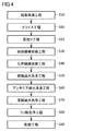
- FIG. 4 is a flowchart schematically showing a method for manufacturing a silicon carbide substrate according to the present embodiment.
- FIG. 5 is a schematic cross-sectional view showing the first step of the method for manufacturing a silicon carbide substrate according to the present embodiment.
- FIG. 6 is a schematic cross-sectional view showing a second step of the method for manufacturing a silicon carbide substrate according to the present embodiment.
- FIG. 7 is a schematic cross-sectional view showing a third step of the method for manufacturing a silicon carbide substrate according to the present embodiment.
- FIG. 8 is a schematic cross-sectional view showing a fourth step of the method for manufacturing a silicon carbide substrate according to the present embodiment.
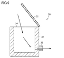
- FIG. 9 is a schematic cross-sectional view showing a fifth step of the method for manufacturing a silicon carbide substrate according to the present embodiment.
- An object of the present disclosure is to provide a silicon carbide substrate having high cleanliness. [Effect of this disclosure] According to the present disclosure, it is possible to provide a silicon carbide substrate having high cleanliness. [Explanation of Embodiments of the present disclosure] First, the embodiments of the present disclosure will be listed and described.
- the silicon carbide substrate 100 includes a first main surface 1, a second main surface 2, and a chamfered portion 6.
- the second main surface 2 is on the opposite side of the first main surface 1.
- the chamfered portion 6 is connected to each of the first main surface 1 and the second main surface 2.
- the maximum diameter is 150 mm or more.
- the surface manganese concentration in the chamfered portion 6 is 1 ⁇ 10 11 atoms / cm 2 or less.
- the arithmetic mean roughness in the chamfered portion 6 may be larger than the arithmetic mean roughness in each of the first main surface 1 and the second main surface 2.
- the surface sodium concentration in the chamfered portion 6 may be 1 ⁇ 10 8 atoms / cm 2 or more.
- the surface sodium concentration in the chamfered portion 6 may be 3 ⁇ 10 11 atoms / cm 2 or less.
- the surface potassium concentration in the chamfered portion 6 may be 1 ⁇ 10 11 atoms / cm 2 or less.
- the surface iron concentration in the chamfered portion 6 may be 1 ⁇ 10 11 atoms / cm 2 or less.
- FIG. 1 is a schematic plan view showing the configuration of the silicon carbide substrate 100 according to the present embodiment.
- FIG. 2 is a schematic cross-sectional view taken along the line II-II of FIG.
- the silicon carbide substrate 100 mainly has a first main surface 1, a second main surface 2, and a chamfered portion 6.
- the second main surface 2 is on the opposite side of the first main surface 1.
- the chamfered portion 6 is connected to each of the first main surface 1 and the second main surface 2.
- Each of the first main surface 1 and the second main surface 2 is a flat surface.
- the first main surface 1 is a surface on which an epitaxial layer (not shown) is formed.
- the silicon carbide substrate 100 is composed of, for example, a polytype 4H hexagonal silicon carbide single crystal.
- the silicon carbide substrate 100 contains n-type impurities such as nitrogen.
- the first main surface 1 is, for example, a surface that is 8 ° or less off with respect to the ⁇ 0001 ⁇ surface or the ⁇ 0001 ⁇ surface. Specifically, the first main surface 1 is, for example, a surface off from the (0001) surface or the (0001) surface by 8 ° or less. The first main surface 1 may be, for example, a surface that is 8 ° or less off from the (000-1) surface or the (000-1) surface. When the first main surface 1 is the (0001) surface, the second main surface 2 is the (000-1) surface.
- the chamfered portion 6 has a first curved region 3, an outer peripheral end portion 5, and a second curved region 4.
- the first curved region 3 is connected to the first main surface 1.
- the first curved region 3 is located outside the first main surface 1.
- the second curved region 4 is connected to the second main surface 2.
- the second curved region 4 is located outside the second main surface 2.
- in the cross section perpendicular to the first main surface 1, each of the first curved region 3 and the second curved region 4 has an arc shape.
- Each of the first curved region 3 and the second curved region 4 is curved so as to project outward.
- the outer peripheral end portion 5 is a portion located on the outermost side in the radial direction parallel to the first main surface 1.
- the outer peripheral end portion 5 is connected to each of the first curved region 3 and the second curved region 4.
- the first curved region 3 is located between the first main surface 1 and the outer peripheral end portion 5.
- the second curved region 4 is located between the second main surface 2 and the outer peripheral end portion 5.
- the outer peripheral end portion 5 has an orientation flat portion 7 and an arc-shaped portion 8.
- the arcuate portion 8 is connected to the orientation flat portion 7.
- the orientation flat portion 7 extends along the first direction 101.
- Each of the first direction 101 and the second direction 102 is parallel to the first main surface 1.
- the second direction 102 is a direction perpendicular to the first direction 101.
- the first direction 101 is, for example, the ⁇ 11-20> direction.
- the second direction 102 is, for example, the ⁇ 1-100> direction.
- the first direction 101 may be, for example, a direction in which the ⁇ 11-20> direction is projected onto the first main surface 1.
- the second direction 102 may be, for example, a direction in which the ⁇ 1-100> direction is projected onto the first main surface 1.
- the maximum diameter (first width W1) of the silicon carbide substrate 100 is 150 mm or more.
- the maximum diameter of the silicon carbide substrate 100 when viewed in the direction perpendicular to the first main surface 1 may be calculated as the diameter of a circle including the arcuate portion 8.
- the first width W1 may be 200 mm or more, or 250 mm or more.
- the upper limit of the first width W1 is not particularly limited, but may be, for example, 300 mm or less.
- the width of the chamfered portion 6 (second width W2) is, for example, 0.1 mm or more and 0.3 mm or less when viewed in the direction perpendicular to the first main surface 1.
- the distance from the boundary between the first main surface 1 and the chamfered portion 6 to the outer peripheral end portion 5 is, for example, 0.1 mm or more when viewed in the direction perpendicular to the first main surface 1. It is 3 mm or less.
- FIG. 3 is an enlarged schematic view of region III of FIG. As shown in FIG. 3, a plurality of steps (grinding marks 9) are formed in the chamfered portion 6.
- the grinding marks 9 are formed, for example, along the circumferential direction.
- the arithmetic mean roughness (Ra) in the chamfered portion 6 is larger than the arithmetic mean roughness in each of the first main surface 1 and the second main surface 2.
- the arithmetic mean roughness on each of the first main surface 1 and the second main surface 2 is, for example, 0.056 nm.
- the arithmetic mean roughness on each of the first main surface 1 and the second main surface 2 may be, for example, 0.03 nm or more and 0.2 nm or less.
- the arithmetic mean roughness (Ra) in the chamfered portion 6 is, for example, 0.1 ⁇ m.
- the arithmetic mean roughness (Ra) in the chamfered portion 6 may be, for example, 0.05 ⁇ m or more and 0.5 ⁇ m or less.
- Arithmetic surface roughness (Ra) can be measured using an atomic force microscope (AFM) or a stylus type surface roughness measuring instrument.
- AFM atomic force microscope
- cantilever for example, a model “NCHV-10V” manufactured by Bruker can be used.
- stylus type surface roughness measuring instrument for example, "Surfcom 1800G” manufactured by Tokyo Seimitsu Co., Ltd. can be used.
- the measurement range of the AFM is the region from the boundary 10 between the first main surface 1 and the chamfered portion 6 to the outer peripheral end portion 5.
- the straight line A connecting the boundary 10 of the first main surface 1 and the chamfered portion 6 and the outer peripheral end portion 5 is set as the reference height.
- the measurement mode is the tapping mode
- the pitch is 40 nm
- the measurement depth is 1.0 ⁇ m.
- the scanning speed is 5 seconds per cycle
- the number of data per scanning line is 512 points
- the number of scanning lines is 512.
- the displacement control of the cantilever is set to, for example, 15.50 nm.
- the concentration of metal impurities in the chamfered portion 6 will be described. Sludge containing manganese tends to adhere to the grinding marks 9.
- sludge containing manganese (Mn) in the chamfered portion 6 is reduced.
- the concentration of manganese in the chamfered portion 6 is 1 ⁇ 10 11 atoms / cm 2 or less.
- the concentration of manganese in the chamfered portion 6 is preferably 1 ⁇ 10 10 atoms / cm 2 or less, and more preferably 1 ⁇ 10 9 atoms / cm 2 or less.
- the lower limit of the manganese concentration in the chamfered portion 6 is not particularly limited, but is, for example, 1 ⁇ 10 8 atoms / cm 2 or more.
- the concentration of sodium (Na) in the chamfered portion 6 is, for example, 1 ⁇ 10 8 atoms / cm 2 or more.
- the concentration of sodium in the chamfered portion 6 may be, for example, 1 ⁇ 10 9 atoms / cm 2 or more, or 1 ⁇ 10 10 atoms / cm 2 or more.
- the upper limit of the sodium concentration in the chamfered portion 6 is not particularly limited, but may be, for example, 3 ⁇ 10 11 atoms / cm 2 or less.
- the concentration of potassium (K) in the chamfered portion 6 is, for example, 1 ⁇ 10 11 atoms / cm 2 or less.
- the concentration of potassium in the chamfered portion 6 may be, for example, 8 ⁇ 10 10 atoms / cm 2 or less, or may be, for example, 6 ⁇ 10 10 atoms / cm 2 or less.
- the lower limit of the potassium concentration in the chamfered portion 6 is not particularly limited, but is, for example, 1 ⁇ 10 8 atoms / cm 2 or more.
- the concentration of iron (Fe) in the chamfered portion 6 is, for example, 1 ⁇ 10 11 atoms / cm 2 or less.
- the iron concentration in the chamfered portion 6 may be, for example, 8 ⁇ 10 10 atoms / cm 2 or less.
- the lower limit of the iron concentration in the chamfered portion 6 is not particularly limited, but is, for example, 1 ⁇ 10 8 atoms / cm 2 or more.
- the concentration of metal impurities can be measured by ICP-MS (Inductively Coupled Plasma Mass Spectrometry).
- ICP-MS8800 manufactured by Aguilent can be used as the measuring device.
- the mass (ng) of the metal impurity element obtained in the measurement is divided by the atomic weight of each element to convert it to the number of moles, and then multiplied by the Avogadro number to convert it to the number of atoms.
- the number of atoms per unit area is converted by dividing the number of atoms by the area of the chamfered portion 6.
- the concentration of metal impurities is the number of atoms per unit area.
- the area of the chamfered portion 6 is about 3.78 cm 2 .
- the area of the chamfered portion 6 has the length of the outer peripheral end portion 5 of the silicon carbide substrate 100 viewed in the direction perpendicular to the first main surface 1 as the long side, and the width of the chamfered portion 6 (second width W2). Is calculated as the area of a rectangle whose short side is (see FIG. 1).
- Manganese may be present on the first main surface 1.
- the concentration of manganese may be 1 ⁇ 10 9 atoms / cm 2 or less.
- the concentration of manganese on the first main surface 1 is lower than the concentration of manganese on the chamfered portion 6.
- Sodium may be present on the first main surface 1.
- the concentration of sodium may be 5 ⁇ 10 10 atoms / cm 2 or less.
- the concentration of sodium on the first main surface 1 is lower than the concentration of sodium on the chamfered portion 6.
- Potassium may be present on the first main surface 1.
- the concentration of potassium may be 2 ⁇ 10 10 atoms / cm 2 or less.
- the concentration of potassium on the first main surface 1 is lower than the concentration of potassium on the chamfered portion 6.
- Iron may be present on the first main surface 1.
- the iron concentration may be 5 ⁇ 10 9 atoms / cm 2 or less.
- the concentration of iron on the first main surface 1 is lower than the concentration of iron on the chamfered portion 6.
- S Sulfur
- the sulfur concentration may be 5 ⁇ 10 10 atoms / cm 2 or more.
- the sulfur concentration may be 1 ⁇ 10 12 atoms / cm 2 or more.
- Chlorine (Cl) may be present on the first main surface 1.
- the concentration of chlorine may be 5 ⁇ 10 10 atoms / cm 2 or more.
- the concentration of chlorine may be 1 ⁇ 10 12 atoms / cm 2 or more.
- the concentration of metal impurities can be measured by a total reflection fluorescent X-ray analyzer.
- the analyzer for example, TXRF-3760 manufactured by Rigaku Co., Ltd. can be used.
- the analyzer has a plurality of excitation X-ray sources, and can measure from Na as a light element to U as a heavy element by using the excitation X-rays most suitable for the measurement element. Specifically, for Na, W-Ma (1.78 keV) excited X-rays are used. For K, S, Fe, Cl and Mn, W-Lb (9.67 keV) excited X-rays are used.
- the X-ray power is, for example, 35 kV-255 mA.
- the incident direction is 39 °.
- the incident angle of W-Ma is 0.500 °.
- the measurement time of W-Ma is 10 seconds / point.
- the incident angle of W-Lb is 0.100 °.
- the measurement time of W-Lb is 10 seconds / point.
- the analyzer has an XY drive stage and can measure the in-plane distribution of the measurement element.
- the first main surface 1 can be divided into 101 regions with equal areas, and the concentration of the measurement element can be measured at the 101 regions.
- the concentration of metal impurities on the first main surface shall be the average value of the concentrations at the 101 locations.
- the concentration of metal impurities is the number of atoms per unit area.
- the manufacturing method of the silicon carbide substrate 100 according to the present embodiment includes a crystal preparation step (S10), a slicing step (S20), a chamfering step (S25), and a double-sided machine polishing step (S30). ), Chemical mechanical polishing step (S40), sulfuric acid overwater cleaning step (S50), ammonia overwater cleaning step (S60), hydrochloric acid overwater cleaning step (S70), and hydrofluoric acid cleaning step (S80). , The drying step (S90) is included.
- the crystal preparation step (S10) is carried out.
- a silicon carbide ingot is formed by a sublimation method.
- the slicing step (S20) is carried out.
- the silicon carbide ingot is cut out on the plurality of silicon carbide substrates 100 by the saw wire.
- the silicon carbide substrate 100 is composed of, for example, a polytype 4H hexagonal silicon carbide single crystal. As shown in FIG. 5, the silicon carbide substrate 100 has a first main surface 1, a second main surface 2, and an outer peripheral end portion 5. At this point, the chamfered portion 6 is not formed.
- the chamfering process (S25) is carried out.
- the grinding device 25 is used.
- the chamfering process for example, diamond abrasive grains are used.
- FIG. 6 the vicinity of the boundary between the first main surface 1 of the silicon carbide substrate 100 and the outer peripheral end portion 5 is pressed against the rotating grinding device 25.
- FIG. 7 the vicinity of the boundary between the first main surface 1 of the silicon carbide substrate 100 and the outer peripheral end portion 5 is pressed against the rotating grinding device 25.
- the chamfered portion 6 is formed on the silicon carbide substrate 100 (see FIG. 2).
- grinding marks may be formed on the chamfered portion 6.
- the double-sided mechanical polishing step (S30) is carried out.
- the silicon carbide substrate 100 is arranged so that the first main surface 1 faces the first surface plate (not shown) and the second main surface 2 corresponds to the second surface plate (not shown). It is placed between the first surface plate and the second surface plate.
- the slurry is introduced between the first main surface 1 and the first surface plate and between the second main surface 2 and the second surface plate.
- the slurry contains, for example, diamond abrasive grains and water.
- the diameter of the diamond abrasive grains is, for example, 0.5 ⁇ m or more and 3 ⁇ m or less.
- a load is applied to the first main surface 1 by the first surface plate, and a load is applied to the second main surface 2 by the second surface plate, so that both surfaces of the silicon carbide substrate 100 are mechanically polished.
- CMP Chemical Mechanical Polishing
- colloidal silica is used as the abrasive grains.
- a polishing solution containing permanganate is used.
- Abrasive cloth is attached to the surface plate.
- the polishing cloth is, for example, a non-woven fabric.
- the processing pressure is, for example, 300 g / cm 2 .
- the flow rate of the polishing liquid is, for example, 50 cc / min.
- the rotation speed of the surface plate is, for example, 40 rpm.
- the processing time is, for example, 2 hours.
- the sulfuric acid hydrogen peroxide cleaning step (S50) is carried out.
- an ultrasonic cleaning device is used.
- the ultrasonic cleaning device 20 mainly includes an ultrasonic generation source 19, a first cleaning tank 12, and a second cleaning tank 13.
- the second cleaning tank 13 is arranged on the first cleaning tank 12.
- the second cleaning tank 13 is hung on the opening of the first cleaning tank 12.
- the first cleaning liquid 14 (specifically, water) is contained in the first cleaning tank 12.
- the second cleaning liquid 15 (specifically, sulfuric acid hydrogen peroxide) is contained in the second cleaning tank 13.
- the silicon carbide substrate 100 is immersed in sulfuric acid hydrogen peroxide.
- the ultrasonic wave generation source 19 is arranged at the bottom of the second cleaning tank 13.
- the second cleaning tank 13 is arranged on the ultrasonic wave generation source 19.
- the silicon carbide substrate 100 is cleaned while the sulfuric acid hydrogen peroxide is irradiated with ultrasonic waves in order to enhance the effect of removing metal impurities.
- the frequency of ultrasonic waves is, for example, 450 kHz or more and 2 MHz or less. Ultrasound promotes a chemical reaction. This enhances the reactivity of metal impurities with sulfuric acid hydrogen peroxide. Further, due to the cavitation effect of ultrasonic irradiation, sludge containing manganese that has entered the grinding marks of the chamfered portion 6 can be effectively removed.
- Sulfuric acid hydrogen peroxide cleaning step (S50), mainly organic substances and metal impurities are removed.
- Sulfuric acid superwater is a solution in which sulfuric acid, hydrogen peroxide solution, and ultrapure water are mixed.
- sulfuric acid for example, concentrated sulfuric acid having a mass percentage concentration of 96% can be used.
- hydrogen peroxide solution for example, a hydrogen peroxide solution having a mass percentage concentration of 30% can be used. The same applies to the hydrogen peroxide solution used in the subsequent steps.
- the volume ratio of sulfuric acid, hydrogen peroxide solution, and ultrapure water contained in sulfuric acid superwater is, for example, 10 (sulfuric acid): 1 (hydrogen peroxide solution): 1 (ulpure water) to 10 (ulpure water) :. 3 (hydrogen peroxide solution): 1 (ultrapure water).
- the volume of sulfuric acid is 10 times the volume of ultrapure water.
- the volume of hydrogen peroxide solution is 1 times or more and 3 times or less the volume of ultrapure water.
- the immersion time of the silicon carbide substrate 100 is, for example, 5 minutes or more.
- the temperature of the sulfuric acid hydrogen peroxide is, for example, room temperature.
- ammonia hydrogen peroxide cleaning step (S60) is carried out.
- Ammonia superwater is a solution in which an aqueous ammonia solution, a hydrogen peroxide solution, and ultrapure water are mixed.
- an aqueous ammonia solution for example, an aqueous ammonia solution having a mass percentage concentration of 28% can be used.
- the silicon carbide substrate 100 may be cleaned while the ammonia hydrogen peroxide is irradiated with ultrasonic waves.
- the volume ratio of the ammonia aqueous solution, the hydrogen peroxide solution, and the ultrapure water contained in the ammonia superwater is 1 (ammonia aqueous solution): 1 (hydrogen hydrogen solution): 5 (ultrapure water) to 1 (ammonia aqueous solution). ): 1 (hydrogenated water): 10 (ultrapure water).
- the volume of the aqueous ammonia solution is 1/10 times or more and 1/5 times or less the volume of ultrapure water.
- the volume of hydrogen peroxide solution is 1/10 times or more and 1/5 times or less of the volume of ultrapure water.
- the immersion time of the silicon carbide substrate 100 is, for example, 5 minutes or more.
- the temperature of the sulfuric acid hydrogen peroxide is, for example, room temperature.
- the hydrochloric acid hydrogen peroxide cleaning step (S70) is carried out.
- the hydrochloric acid overwater is a solution in which hydrochloric acid, hydrogen peroxide solution, and ultrapure water are mixed.
- hydrochloric acid for example, concentrated hydrochloric acid having a mass percentage concentration of 98% can be used.
- the silicon carbide substrate 100 may be cleaned while the hydrochloric acid hydrogen peroxide is irradiated with ultrasonic waves.
- the volume ratio of hydrochloric acid, hydrogen peroxide solution, and ultrapure water contained in hydrochloric acid superwater is, for example, 1 (hydrochloric acid): 1 (hydrogen peroxide solution): 5 (ultrapure water) to 1 (hydrochloric acid) :. 1 (hydrochloric acid solution): 10 (ultrapure water).
- the volume of hydrochloric acid is 1/10 times or more and 1/5 times or less the volume of ultrapure water.
- the volume of hydrogen peroxide solution is 1/10 times or more and 1/5 times or less of the volume of ultrapure water.
- the immersion time of the silicon carbide substrate 100 is, for example, 5 minutes or more.
- the temperature of the sulfuric acid hydrogen peroxide is, for example, room temperature.
- the hydrofluoric acid cleaning step (S80) is carried out.
- the silicon oxide film is removed by hydrofluoric acid, and the surface is terminated with fluorine.
- the concentration of hydrofluoric acid in the mixed solution of hydrofluoric acid and ultrapure water is, for example, 10% or more and 40% or less.
- the immersion time of the silicon carbide substrate 100 is, for example, 5 minutes or more.
- the temperature of the sulfuric acid hydrogen peroxide is, for example, room temperature.
- the silicon carbide substrate 100 may be cleaned while the hydrofluoric acid is irradiated with ultrasonic waves.
- the drying step (S90) is carried out.
- the silicon carbide substrate 100 is dried using, for example, a spin dryer 30.
- the spin dryer 30 includes a main body 31, a lid 32, an opening 34, and an exhaust port 33.
- the spin dryer 30 is arranged in a clean room equivalent to class 100.
- air is passed through the opening 34 of the spin dryer 30 toward the exhaust port 33 with the lid 32 of the spin dryer 30 open.
- the volume of the main body is, for example, 127,000 cm 3 .
- the area of the opening 34 is, for example, 2700 cm 2 .
- the amount of air passing is, for example, 60 m 3 .
- the silicon carbide substrate 100 is arranged on the main body 31 of the spin dryer 30, and the lid 32 is closed.
- the silicon carbide substrate 100 rotates around a rotation axis substantially perpendicular to the first main surface 1 in a state of being decompressed through the exhaust port 33.
- the rotation speed of the silicon carbide substrate 100 is, for example, 800 rpm.
- the rotation time is, for example, 300 seconds.
- the cleaning liquid adhering to the silicon carbide substrate 100 is removed by centrifugal force.
- a polishing liquid containing permanganate has been used in the polishing process of the silicon carbide substrate 100.
- the polishing liquid containing permanganate has a high polishing efficiency with respect to the silicon carbide substrate 100, but has a property of easily remaining as an impurity on the silicon carbide substrate 100.
- the potassium permanganate salt becomes muddy sludge and easily adheres to the silicon carbide substrate 100.
- a grinding mark 9 is formed on the chamfered portion 6 of the silicon carbide substrate 100 by the grinding process in the chamfering step (S25). Sludge containing permanganate easily enters the grinding mark 9 together with abrasive grains and the like. Once sludge has entered the grinding mark 9, it is difficult to remove it by a general cleaning method.
- the silicon carbide substrate 100 is cleaned while the sulfuric acid hydrogen peroxide is irradiated with ultrasonic waves.
- Ultrasound promotes a chemical reaction. This enhances the reactivity of metal impurities such as manganese with sulfuric acid hydrogen peroxide.
- metal impurities such as manganese with sulfuric acid hydrogen peroxide.
- sludge containing manganese that has entered the grinding mark 9 of the chamfered portion 6 can be effectively removed. Therefore, the concentration of manganese in the chamfered portion 6 can be reduced.
- the concentration of manganese in the chamfered portion 6 can be set to 1 ⁇ 10 11 atoms / cm 2 or less.
- the silicon carbide substrate 100 having high cleanliness can be obtained.
- metal impurities such as manganese.
- sample preparation First, the silicon carbide substrate 100 according to sample 1 and the silicon carbide substrate 100 according to sample 2 were prepared.
- the silicon carbide substrate 100 according to sample 1 is an example.
- the silicon carbide substrate 100 according to sample 2 is a comparative example.
- the maximum diameter (diameter) of the silicon carbide substrate 100 was set to 150 mm.
- the silicon carbide substrate 100 according to sample 1 was manufactured by the manufacturing method according to the present embodiment. Specifically, in the sulfuric acid hydrogen peroxide cleaning step (S50), ultrasonic waves were applied to the sulfuric acid hydrogen peroxide. The frequency of the ultrasonic wave was 950 kHz. The volume ratio of sulfuric acid, hydrogen peroxide solution, and ultrapure water contained in sulfuric acid superwater was 10 (sulfuric acid): 1 (hydrogen peroxide solution): 1 (ultrapure water). The immersion time of the silicon carbide substrate 100 was 30 minutes. The temperature of the sulfuric acid hydrogen peroxide was room temperature.
- the number of atoms per unit area was converted by dividing the number of atoms by the area of the chamfered portion 6.
- the area of the chamfered portion 6 of the silicon carbide substrate 100 was 3.78 cm 2 .
- the arithmetic mean roughness (Ra) at the chamfered portion was measured using a stylus type surface roughness measuring device.
- a stylus type surface roughness measuring device Surfcom 1800G manufactured by Tokyo Seimitsu Co., Ltd. was used.
- Table 1 shows the concentration of metal impurities in the chamfered portion 6.
- the concentration of sodium (Na) in the chamfered portion 6 of the silicon carbide substrate 100 according to the sample 1 was 11.0 ⁇ 10 10 atoms / cm 2 .
- the concentration of potassium (K) was 4.7 ⁇ 10 10 atoms / cm 2 .
- Manganese (Mn) was not detected.
- the concentration of iron (Fe) was 7.2 ⁇ 10 10 atoms / cm 2 .
- the concentration of sodium (Na) in the chamfered portion 6 of the silicon carbide substrate 100 according to the sample 2 was 46.0 ⁇ 10 10 atoms / cm 2 .
- the concentration of potassium (K) was 4.1 ⁇ 10 10 atoms / cm 2 .
- Manganese (Mn) was 12.0 ⁇ 10 10 atoms / cm 2 .
- the concentration of iron (Fe) was 21.0 ⁇ 10 10 atoms / cm 2 .
- Table 2 shows the arithmetic mean roughness (Ra) in the chamfered portion 6.
- the arithmetic mean roughness (Ra) of the chamfered portion 6 of the silicon carbide substrate 100 according to the sample 1 was 0.1 ⁇ m.
- the arithmetic mean roughness (Ra) of the chamfered portion 6 of the silicon carbide substrate 100 according to the sample 2 was 0.1 ⁇ m.
Landscapes
- Chemical & Material Sciences (AREA)
- Engineering & Computer Science (AREA)
- Crystallography & Structural Chemistry (AREA)
- Materials Engineering (AREA)
- Metallurgy (AREA)
- Organic Chemistry (AREA)
- Inorganic Chemistry (AREA)
- Crystals, And After-Treatments Of Crystals (AREA)
- Mechanical Treatment Of Semiconductor (AREA)
- Cleaning Or Drying Semiconductors (AREA)
Abstract
炭化珪素基板は、第1主面と、第2主面と、面取り部とを有している。第2主面は、第1主面と反対側にある。面取り部は、第1主面および第2主面の各々に連なっている。最大径が150mm以上である。面取り部における表面マンガン濃度は、1×10¹¹atoms/cm2以下である。
Description
本開示は、炭化珪素基板に関する。本出願は、2019年5月17日に出願した日本特許出願である特願2019-093883号に基づく優先権を主張する。当該日本特許出願に記載された全ての記載内容は、参照によって本明細書に援用される。
国際公開第2016/063632号(特許文献1)には、炭化珪素基板を洗浄する方法が記載されている。
本開示に係る炭化珪素基板は、第1主面と、第2主面と、面取り部とを備えている。第2主面は、第1主面と反対側にある。面取り部は、第1主面および第2主面の各々に連なっている。最大径が150mm以上である。面取り部における表面マンガン濃度は、1×10¹¹atoms/cm2以下である。
[本開示が解決しようとする課題]
本開示の目的は、清浄度の高い炭化珪素基板を提供することである。
[本開示の効果]
本開示によれば、清浄度の高い炭化珪素基板を提供することができる。
[本開示の実施形態の説明]
最初に本開示の実施形態を列挙して説明する。
本開示の目的は、清浄度の高い炭化珪素基板を提供することである。
[本開示の効果]
本開示によれば、清浄度の高い炭化珪素基板を提供することができる。
[本開示の実施形態の説明]
最初に本開示の実施形態を列挙して説明する。
(1)本開示に係る炭化珪素基板100は、第1主面1と、第2主面2と、面取り部6とを備えている。第2主面2は、第1主面1と反対側にある。面取り部6は、第1主面1および第2主面2の各々に連なっている。最大径は150mm以上である。面取り部6における表面マンガン濃度は、1×10¹¹atoms/cm2以下である。
(2)上記(1)に係る炭化珪素基板100において、面取り部6における算術平均粗さは、第1主面1および第2主面2の各々における算術平均粗さよりも大きくてもよい。
(3)上記(1)または(2)に係る炭化珪素基板100において、面取り部6における表面ナトリウム濃度は、1×10⁸atoms/cm2以上であってもよい。
(4)上記(1)から(3)のいずれかに係る炭化珪素基板100において、面取り部6における表面ナトリウム濃度は、3×10¹¹atoms/cm2以下であってもよい。
(5)上記(1)から(4)のいずれかに係る炭化珪素基板100において、面取り部6における表面カリウム濃度は、1×10¹¹atoms/cm2以下であってもよい。
(6)上記(1)から(5)のいずれかに係る炭化珪素基板100において、面取り部6における表面鉄濃度は、1×10¹¹atoms/cm2以下であってもよい。
[本開示の実施形態の詳細]
以下、図面に基づいて本開示の実施形態を説明する。なお、以下の図面において同一または相当する部分には同一の参照番号を付し、その説明は繰返さない。本明細書中の結晶学的記載においては、個別方位を[]、集合方位を<>、個別面を()、集合面を{}でそれぞれ示している。また、負の指数については、結晶学上、”-”(バー)を数字の上に付けることになっているが、本明細書中では、数字の前に負の符号を付けている。
[本開示の実施形態の詳細]
以下、図面に基づいて本開示の実施形態を説明する。なお、以下の図面において同一または相当する部分には同一の参照番号を付し、その説明は繰返さない。本明細書中の結晶学的記載においては、個別方位を[]、集合方位を<>、個別面を()、集合面を{}でそれぞれ示している。また、負の指数については、結晶学上、”-”(バー)を数字の上に付けることになっているが、本明細書中では、数字の前に負の符号を付けている。
<炭化珪素基板の構成>
まず、本実施形態に係る炭化珪素基板100の構成について説明する。図1は、本実施形態に係る炭化珪素基板100の構成を示す平面模式図である。図2は、図1のII-II線に沿った断面模式図である。
まず、本実施形態に係る炭化珪素基板100の構成について説明する。図1は、本実施形態に係る炭化珪素基板100の構成を示す平面模式図である。図2は、図1のII-II線に沿った断面模式図である。
図1および図2に示されるように、本実施形態に係る炭化珪素基板100は、第1主面1と、第2主面2と、面取り部6とを主に有している。第2主面2は、第1主面1と反対側にある。面取り部6は、第1主面1および第2主面2の各々に連なっている。第1主面1および第2主面2の各々は、平坦面である。第1主面1は、エピタキシャル層(図示せず)が形成される面である。炭化珪素基板100は、たとえばポリタイプ4Hの六方晶炭化珪素単結晶から構成されている。炭化珪素基板100はたとえば窒素などのn型不純物を含む。
第1主面1は、たとえば{0001}面または{0001}面に対して8°以下オフした面である。具体的には、第1主面1は、たとえば(0001)面または(0001)面に対して8°以下オフした面である。第1主面1は、たとえば(000-1)面または(000-1)面に対して8°以下オフした面であってもよい。第1主面1が(0001)面の場合、第2主面2は(000-1)面である。
図2に示されるように、面取り部6は、第1湾曲領域3と、外周端部5と、第2湾曲領域4とを有する。第1湾曲領域3は、第1主面1に連なっている。第1湾曲領域3は、第1主面1よりも外側に位置している。第2湾曲領域4は、第2主面2に連なっている。第2湾曲領域4は、第2主面2よりも外側に位置している。図2に示されるように、第1主面1に対して垂直な断面において、第1湾曲領域3および第2湾曲領域4の各々は、円弧状である。第1湾曲領域3および第2湾曲領域4の各々は、外側に向かって突出するように湾曲している。
外周端部5は、第1主面1に平行な径方向において最も外側に位置している部分である。外周端部5は、第1湾曲領域3および第2湾曲領域4の各々に連なっている。径方向において、第1湾曲領域3は、第1主面1と外周端部5との間に位置している。同様に、径方向において、第2湾曲領域4は、第2主面2と外周端部5との間に位置している。
図1に示されるように、外周端部5は、オリエンテーションフラット部7と、円弧状部8とを有している。円弧状部8は、オリエンテーションフラット部7に連なっている。オリエンテーションフラット部7は、第1方向101に沿って延在している。第1方向101および第2方向102の各々は、第1主面1に平行である。第2方向102は、第1方向101に対して垂直な方向である。第1方向101は、たとえば<11-20>方向である。第2方向102は、たとえば<1-100>方向である。
第1主面1が{0001}面に対して傾斜している場合、第1方向101は、たとえば<11-20>方向を第1主面1に射影した方向であってもよい。第1主面1が{0001}面に対して傾斜している場合、第2方向102は、たとえば<1-100>方向を第1主面1に射影した方向であってもよい。
図1に示されるように、炭化珪素基板100の最大径(第1幅W1)は、150mm以上である。第1主面1に対して垂直な方向に見て、炭化珪素基板100の最大径は、円弧状部8を含む円の直径として算出されてもよい。第1幅W1は、200mm以上であってもよいし、250mm以上であってもよい。第1幅W1の上限は、特に限定されないが、たとえば300mm以下であってもよい。
図1に示されるように、第1主面1に対して垂直な方向に見て、面取り部6の幅(第2幅W2)は、たとえば0.1mm以上0.3mm以下である。別の観点から言えば、第1主面1に対して垂直な方向に見て、第1主面1と面取り部6の境界から外周端部5までの距離は、たとえば0.1mm以上0.3mm以下である。
図3は、図2の領域IIIの拡大模式図である。図3に示されるように、面取り部6には、複数の段差(研削痕9)が形成されている。研削痕9は、たとえば周方向に沿って形成されている。
面取り部6には、研削痕9が形成されている。そのため、面取り部6における算術平均粗さ(Ra)は、第1主面1および第2主面2の各々における算術平均粗さよりも大きくなる。第1主面1および第2主面2の各々における算術平均粗さは、たとえば0.056nmである。第1主面1および第2主面2の各々における算術平均粗さは、たとえば0.03nm以上0.2nm以下であってもよい。面取り部6における算術平均粗さ(Ra)は、たとえば0.1μmである。面取り部6における算術平均粗さ(Ra)は、たとえば0.05μm以上0.5μm以下であってもよい。
次に、算術平均粗さ(Ra)の測定方法について説明する。
算術表面粗さ(Ra)は、原子間力顕微鏡(AFM:Atomic Force Microscope)または触針式表面粗さ測定器を用いて測定することができる。AFMとしては、たとえばVeeco社製の「Dimension300」を用いることができる。カンチレバー(探針)としては、たとえば、Bruker社製の型式「NCHV-10V」を用いることができる。触針式表面粗さ測定器としては、たとえば東京精密社製の「サーフコム1800G」を用いることができる。
算術表面粗さ(Ra)は、原子間力顕微鏡(AFM:Atomic Force Microscope)または触針式表面粗さ測定器を用いて測定することができる。AFMとしては、たとえばVeeco社製の「Dimension300」を用いることができる。カンチレバー(探針)としては、たとえば、Bruker社製の型式「NCHV-10V」を用いることができる。触針式表面粗さ測定器としては、たとえば東京精密社製の「サーフコム1800G」を用いることができる。
AFMの測定範囲は、第1主面1と面取り部6の境界10から外周端部5までの領域とする。第1主面1と面取り部6の境界10と外周端部5とを繋ぐ直線Aが基準高さとされる。AFMの測定条件としては、たとえば測定モードをタッピングモードとし、ピッチを40nmおよび測定深さを1.0μmとする。タッピングモードでのサンプリングは、たとえば走査速度を1周期当たり5秒とし、1走査ラインあたりのデータ数を512ポイントとし、かつ、走査ライン数を512とする。また、カンチレバーの変位制御は、たとえば15.50nmに設定する。
次に、面取り部6における金属不純物の濃度について説明する。
研削痕9にはマンガンを含むスラッジが付着しやすい。本実施形態に係る炭化珪素基板100においては、面取り部6におけるマンガン(Mn)を含むスラッジが低減されている。具体的には、面取り部6におけるマンガンの濃度は、1×10¹¹atoms/cm2以下である。面取り部6におけるマンガンの濃度は、好ましくは1×1010atoms/cm2以下であり、さらに好ましくは1×109atoms/cm2以下である。面取り部6におけるマンガンの濃度の下限は、特に限定されないが、たとえば1×108atoms/cm2以上である。
研削痕9にはマンガンを含むスラッジが付着しやすい。本実施形態に係る炭化珪素基板100においては、面取り部6におけるマンガン(Mn)を含むスラッジが低減されている。具体的には、面取り部6におけるマンガンの濃度は、1×10¹¹atoms/cm2以下である。面取り部6におけるマンガンの濃度は、好ましくは1×1010atoms/cm2以下であり、さらに好ましくは1×109atoms/cm2以下である。面取り部6におけるマンガンの濃度の下限は、特に限定されないが、たとえば1×108atoms/cm2以上である。
本実施形態に係る炭化珪素基板100においては、面取り部6におけるナトリウム(Na)の濃度は、たとえば1×10⁸atoms/cm2以上である。面取り部6におけるナトリウムの濃度は、たとえば1×109atoms/cm2以上であってもよいし、1×1010atoms/cm2以上であってもよい。面取り部6におけるナトリウムの濃度の上限は、特に限定されないが、たとえば3×1011atoms/cm2以下であってもよい。
本実施形態に係る炭化珪素基板100においては、面取り部6におけるカリウム(K)の濃度は、たとえば1×10¹¹atoms/cm2以下である。面取り部6におけるカリウムの濃度は、たとえば8×1010atoms/cm2以下であってもよいし、たとえば6×1010atoms/cm2以下であってもよい。面取り部6におけるカリウムの濃度の下限は、特に限定されないが、たとえば1×108atoms/cm2以上である。
本実施形態に係る炭化珪素基板100においては、面取り部6における鉄(Fe)の濃度は、たとえば1×10¹¹atoms/cm2以下である。面取り部6における鉄の濃度は、たとえば8×1010atoms/cm2以下であってもよい。面取り部6における鉄の濃度の下限は、特に限定されないが、たとえば1×108atoms/cm2以上である。
次に、面取り部6における金属不純物の濃度の測定方法について説明する。
まず、水平型基板検査装置を用いて、炭化珪素基板100の面取り部6の全周(オリエンテーションフラット部7を除く)に酸を滴下することにより、面取り部6上の金属不純物が酸に取り込まれる。次に、面取り部6の全周から金属不純物を含む酸が全量回収される。なお試料調製は、クラス100のクリーンルーム内に設置したクラス10のクリーンドラフト内で実施される。
まず、水平型基板検査装置を用いて、炭化珪素基板100の面取り部6の全周(オリエンテーションフラット部7を除く)に酸を滴下することにより、面取り部6上の金属不純物が酸に取り込まれる。次に、面取り部6の全周から金属不純物を含む酸が全量回収される。なお試料調製は、クラス100のクリーンルーム内に設置したクラス10のクリーンドラフト内で実施される。
金属不純物の濃度は、ICP-MS(Inductively Coupled Plasma Mass Spectrometry)により測定することができる。測定装置として、たとえばAgillent社製のICP-MS8800を用いることができる。測定で得られた金属不純物元素の質量(ng)を各元素の原子量で除してモル数に換算後、アボガドロ数を乗じて原子数に変換する。次に、当該原子数を面取り部6の面積で除することにより、単位面積当たりの原子数が換算される。金属不純物の濃度は、単位面積当たりの原子数のことである。なお、炭化珪素基板100の最大径が150mmの場合、面取り部6の面積は、約3.78cm2となる。面取り部6の面積は、第1主面1に対して垂直な方向に見た炭化珪素基板100の外周端部5の長さを長辺とし、かつ面取り部6の幅(第2幅W2)を短辺とする長方形の面積として算出される(図1参照)。
次に、第1主面1における金属不純物の濃度について説明する。
第1主面1には、マンガンが存在していてもよい。第1主面1において、マンガンの濃度は、1×10⁹atoms/cm2以下であってもよい。第1主面1におけるマンガンの濃度は、面取り部6におけるマンガンの濃度よりも低い。
第1主面1には、マンガンが存在していてもよい。第1主面1において、マンガンの濃度は、1×10⁹atoms/cm2以下であってもよい。第1主面1におけるマンガンの濃度は、面取り部6におけるマンガンの濃度よりも低い。
第1主面1には、ナトリウムが存在していてもよい。第1主面1において、ナトリウムの濃度は、5×10¹⁰atoms/cm2以下であってもよい。第1主面1におけるナトリウムの濃度は、面取り部6におけるナトリウムの濃度よりも低い。
第1主面1には、カリウムが存在していてもよい。第1主面1において、カリウムの濃度は、2×10¹⁰atoms/cm2以下であってもよい。第1主面1におけるカリウムの濃度は、面取り部6におけるカリウムの濃度よりも低い。
第1主面1には、鉄が存在していてもよい。第1主面1において、鉄の濃度は、5×10⁹atoms/cm2以下であってもよい。第1主面1における鉄の濃度は、面取り部6における鉄の濃度よりも低い。
第1主面1には、硫黄(S)が存在していてもよい。第1主面1において、硫黄の濃度は、5×10¹⁰atoms/cm2以上であってもよい。第1主面1において、硫黄の濃度は、1×1012atoms/cm2以上であってもよい。
第1主面1には塩素(Cl)が存在していてもよい。第1主面1において、塩素の濃度は、5×10¹⁰atoms/cm2以上であってもよい。第1主面1において、塩素の濃度は、1×1012atoms/cm2以上であってもよい。
次に、第1主面1における金属不純物の濃度の測定方法について説明する。
金属不純物の濃度は、全反射蛍光X線分析装置により測定することができる。分析装置として、たとえば株式会社リガク製のTXRF-3760を用いることができる。当該分析装置は、複数の励起X線源を有しており、測定元素に最適な励起X線を用いて軽元素のNaから重元素のUまでを測定することができる。具体的には、Naに対しては、W-Ma(1.78keV)の励起X線が用いられる。K、S、Fe、ClおよびMnに対しては、W-Lb(9.67keV)の励起X線が用いられる。
金属不純物の濃度は、全反射蛍光X線分析装置により測定することができる。分析装置として、たとえば株式会社リガク製のTXRF-3760を用いることができる。当該分析装置は、複数の励起X線源を有しており、測定元素に最適な励起X線を用いて軽元素のNaから重元素のUまでを測定することができる。具体的には、Naに対しては、W-Ma(1.78keV)の励起X線が用いられる。K、S、Fe、ClおよびMnに対しては、W-Lb(9.67keV)の励起X線が用いられる。
X線パワーは、たとえば35kV-255mAである。入射方位は、39°である。W-Maの入射角度は、0.500°である。W-Maの測定時間は、10秒/ポイントである。W-Lbの入射角度は、0.100°である。W-Lbの測定時間は、10秒/ポイントである。また当該分析装置は、XY駆動ステージを有しており、測定元素の面内分布を測定することができる。たとえば第1主面1を101箇所の領域に等面積で分割し、当該101箇所において測定元素の濃度を測定することができる。第1主面における金属不純物の濃度は、当該101箇所の濃度の平均値とする。金属不純物の濃度は、単位面積当たりの原子数のことである。
<炭化珪素基板の製造方法>
次に、本実施形態に係る炭化珪素基板100の製造方法について説明する。図4に示されるように、本実施形態に係る炭化珪素基板100の製造方法は、結晶準備工程(S10)と、スライス工程(S20)と、面取り工程(S25)と、両面機械研磨工程(S30)と、化学機械研磨工程(S40)と、硫酸過水洗浄工程(S50)と、アンモニア過水洗浄工程(S60)と、塩酸過水洗浄工程(S70)と、フッ酸洗浄工程(S80)と、乾燥工程(S90)とを含む。
次に、本実施形態に係る炭化珪素基板100の製造方法について説明する。図4に示されるように、本実施形態に係る炭化珪素基板100の製造方法は、結晶準備工程(S10)と、スライス工程(S20)と、面取り工程(S25)と、両面機械研磨工程(S30)と、化学機械研磨工程(S40)と、硫酸過水洗浄工程(S50)と、アンモニア過水洗浄工程(S60)と、塩酸過水洗浄工程(S70)と、フッ酸洗浄工程(S80)と、乾燥工程(S90)とを含む。
まず、結晶準備工程(S10)が実施される。結晶準備工程(S10)においては、たとえば昇華法により、炭化珪素インゴットが形成される。次に、スライス工程(S20)が実施される。スライス工程(S20)においては、炭化珪素インゴットがソーワイヤーによって複数の炭化珪素基板100に切り出される。炭化珪素基板100は、たとえばポリタイプ4Hの六方晶炭化珪素単結晶から構成されている。図5に示されるように、炭化珪素基板100は、第1主面1と、第2主面2と、外周端部5とを有している。この時点においては、面取り部6は形成されていない。
次に、面取り工程(S25)が実施される。面取り工程(S25)においては、研削装置25が用いられる。面取り工程においては、たとえばダイヤモンド砥粒が用いられる。図6に示されるように、回転している研削装置25に、炭化珪素基板100の第1主面1と外周端部5との境界付近が押し当てられる。同様に、図7に示されるように、回転している研削装置25に、炭化珪素基板100の第1主面1と外周端部5との境界付近が押し当てられる。以上により、炭化珪素基板100に面取り部6が形成される(図2参照)。面取り工程(S25)において、面取り部6に研削痕が形成され得る。
次に、両面機械研磨工程(S30)が実施される。具体的には、第1主面1が第1定盤(図示せず)に対向し、かつ第2主面2が第2定盤(図示せず)に対応するように炭化珪素基板100が第1定盤と第2定盤との間に配置される。次に、第1主面1と第1定盤の間および第2主面2と第2定盤との間にスラリーが導入される。スラリーは、たとえばダイヤモンド砥粒と水とを含む。ダイヤモンド砥粒の径は、たとえば0.5μm以上3μm以下である。第1定盤によって第1主面1に荷重が加えられ、かつ第2定盤によって第2主面2に荷重が加えられることにより、炭化珪素基板100の両面に対して機械研磨が行われる。
次に、化学機械研磨工程(S40)が実施される。具体的には、まず炭化珪素基板100の第1主面1においてCMP(Chemical Mechanical Polishing)が行われる。砥粒として、たとえばコロイダルシリカが用いられる。過マンガン酸塩を含む研磨液が使用される。定盤に研磨布が取り付けられる。研磨布は、たとえば不織布である。加工圧は、たとえば300g/cm2である。研磨液の流量は、たとえば50cc/分である。定盤の回転数は、たとえば40rpmである。加工時間は、たとえば2時間である。
次に、硫酸過水洗浄工程(S50)が実施される。硫酸過水洗浄工程(S50)においては、超音波洗浄装置が用いられる。図8に示されるように、超音波洗浄装置20は、超音波発生源19と、第1洗浄槽12と、第2洗浄槽13とを主に有している。第2洗浄槽13は、第1洗浄槽12上に配置されている。第2洗浄槽13は、第1洗浄槽12の開口部に掛けられている。第1洗浄槽12には、第1洗浄液14(具体的には水)が入れられている。第2洗浄槽13には、第2洗浄液15(具体的には硫酸過水)が入れられている。炭化珪素基板100は、硫酸過水に浸漬されている。超音波発生源19は、第2洗浄槽13の底に配置されている。第2洗浄槽13は、超音波発生源19上に配置されている。
硫酸過水洗浄工程(S50)においては、金属不純物の除去効果を高めるために、硫酸過水に超音波が照射された状態で炭化珪素基板100が洗浄される。超音波の周波数は、たとえば450kHz以上2MHz以下である。超音波によって化学的反応が促進される。これにより、金属不純物の硫酸過水に対する反応性が高められる。また超音波照射によるキャビテーション効果により、面取り部6の研削痕に入り込んだマンガンを含むスラッジを効果的に除去することができる。
硫酸過水洗浄工程(S50)においては、主に有機物および金属不純物などが除去される。硫酸過水は、硫酸と、過酸化水素水と、超純水とが混合された溶液である。硫酸としては、たとえば質量百分率濃度が96%の濃硫酸を使用することができる。過酸化水素水としては、たとえば質量百分率濃度が30%の過酸化水素水を用いることができる。以降の工程で用いられる過酸化水素水についても同様である。
硫酸過水が含む、硫酸と、過酸化水素水と、超純水との体積比率は、たとえば10(硫酸):1(過酸化水素水):1(超純水)から10(硫酸):3(過酸化水素水):1(超純水)である。言い換えれば、硫酸の体積は超純水の体積の10倍である。過酸化水素水の体積は超純水の体積の1倍以上3倍以下である。炭化珪素基板100の浸漬時間は、たとえば5分以上である。硫酸過水の温度は、たとえば室温である。
次に、アンモニア過水洗浄工程(S60)が実施される。アンモニア過水洗浄工程(S60)においては、主に研磨剤および埃が除去される。アンモニア過水は、アンモニア水溶液と、過酸化水素水と、超純水とが混合された溶液である。アンモニア水溶液としては、たとえば質量百分率濃度が28%のアンモニア水溶液を使用することができる。アンモニア過水洗浄工程(S60)においては、アンモニア過水に超音波が照射された状態で炭化珪素基板100が洗浄されてもよい。
アンモニア過水が含む、アンモニア水溶液と、過酸化水素水と、超純水との体積比率は、1(アンモニア水溶液):1(過酸化水素水):5(超純水)から1(アンモニア水溶液):1(過酸化水素水):10(超純水)である。言い換えれば、アンモニア水溶液の体積は超純水の体積の1/10倍以上1/5倍以下である。また、過酸化水素水の体積は超純水の体積の1/10倍以上1/5倍以下である。炭化珪素基板100の浸漬時間は、たとえば5分以上である。硫酸過水の温度は、たとえば室温である。
次に、塩酸過水洗浄工程(S70)が実施される。塩酸過水洗浄工程(S70)においては、主に重金属が除去される、塩酸過水は、塩酸と、過酸化水素水と、超純水とが混合された溶液である。塩酸としては、たとえば質量百分率濃度が98%の濃塩酸を使用することができる。塩酸過水洗浄工程(S70)においては、塩酸過水に超音波が照射された状態で炭化珪素基板100が洗浄されてもよい。
塩酸過水が含む、塩酸と、過酸化水素水と、超純水との体積比率は、たとえば1(塩酸):1(過酸化水素水):5(超純水)から1(塩酸):1(過酸化水素水):10(超純水)である。言い換えれば、塩酸の体積は超純水の体積の1/10倍以上1/5倍以下である。また、過酸化水素水の体積は超純水の体積の1/10倍以上1/5倍以下である。炭化珪素基板100の浸漬時間は、たとえば5分以上である。硫酸過水の温度は、たとえば室温である。
次に、フッ酸洗浄工程(S80)が実施される。フッ酸洗浄工程(S80)においては、フッ酸によりシリコン酸化膜が除去され、表面がフッ素で終端される。フッ酸と超純水とが混合された混合液におけるフッ酸の濃度は、たとえば10%以上40%以下である。炭化珪素基板100の浸漬時間は、たとえば5分以上である。硫酸過水の温度は、たとえば室温である。フッ酸洗浄工程(S80)においては、フッ酸に超音波が照射された状態で炭化珪素基板100が洗浄されてもよい。
次に、乾燥工程(S90)が実施される。乾燥工程(S90)においては、たとえばスピン乾燥機30を用いて、炭化珪素基板100が乾燥させられる。図9に示されるように、スピン乾燥機30は、本体部31と、蓋32と、開口部34と、排気口33とを備えている。スピン乾燥機30は、クラス100相当のクリーンルームに配置されている。スピン乾燥機30へ炭化珪素基板100を投入する前に、スピン乾燥機30の蓋32を開いた状態で、スピン乾燥機30の開口部34から排気口33に向かってエアーを通過させる。本体部の容積は、たとえば127000cm3である。開口部34の面積は、たとえば2700cm2である。エアーの通過量は、たとえば60m3である。
次に、炭化珪素基板100がスピン乾燥機30の本体部31に配置され、蓋32が閉められる。炭化珪素基板100は、排気口33を通して減圧した状態で、第1主面1に対してほぼ垂直な回転軸の周りを回転する。炭化珪素基板100の回転数は、たとえば800rpmである。回転時間は、たとえば300秒である。これにより、炭化珪素基板100に付着していた洗浄液が遠心力によって除去される。
次に、本実施形態の作用効果について説明する。
近年、研磨効果を高めるため、炭化珪素基板100の研磨工程において、過マンガン酸塩を含む研磨液が利用されている。過マンガン酸塩を含む研磨液は、炭化珪素基板100に対する研磨効率が高い一方で、不純物として炭化珪素基板100に残りやすい性質を有する。たとえば過マンガン酸カリウムは着色料の原料として用いられていることからも分かるように、過マンガン酸カリウム塩は泥状のスラッジとなって、炭化珪素基板100に付着しやすい。
近年、研磨効果を高めるため、炭化珪素基板100の研磨工程において、過マンガン酸塩を含む研磨液が利用されている。過マンガン酸塩を含む研磨液は、炭化珪素基板100に対する研磨効率が高い一方で、不純物として炭化珪素基板100に残りやすい性質を有する。たとえば過マンガン酸カリウムは着色料の原料として用いられていることからも分かるように、過マンガン酸カリウム塩は泥状のスラッジとなって、炭化珪素基板100に付着しやすい。
特に、炭化珪素基板100の面取り部6には、面取り工程(S25)の研削加工によって研削痕9が形成されている。過マンガン酸塩を含むスラッジは、砥粒などと共に研削痕9に入り込みやすい。一旦研削痕9にスラッジが入り込むと、一般的な洗浄方法で取り除くことは困難である。
本実施形態に係る炭化珪素基板100の硫酸過水洗浄工程(S50)においては、硫酸過水に超音波が照射された状態で炭化珪素基板100が洗浄される。超音波によって化学的反応が促進される。これにより、マンガンなどの金属不純物の硫酸過水に対する反応性が高められる。また超音波照射によるキャビテーション効果により、面取り部6の研削痕9に入り込んだマンガンを含むスラッジを効果的に除去することができる。そのため、面取り部6におけるマンガンの濃度を低減することができる。具体的には、面取り部6におけるマンガンの濃度を1×10¹¹atoms/cm2以下とすることができる。これにより、清浄度の高い炭化珪素基板100が得られる。結果として、炭化珪素基板100を使用して炭化珪素半導体装置を作製した際、マンガンなどの金属不純物によって炭化珪素半導体装置の電気特性が劣化することを抑制することができる。
(サンプル準備)
まず、サンプル1に係る炭化珪素基板100と、サンプル2に係る炭化珪素基板100とが準備された。サンプル1に係る炭化珪素基板100は、実施例である。サンプル2に係る炭化珪素基板100は、比較例である。炭化珪素基板100の最大径(直径)は、150mmとした。
まず、サンプル1に係る炭化珪素基板100と、サンプル2に係る炭化珪素基板100とが準備された。サンプル1に係る炭化珪素基板100は、実施例である。サンプル2に係る炭化珪素基板100は、比較例である。炭化珪素基板100の最大径(直径)は、150mmとした。
サンプル1に係る炭化珪素基板100は、本実施形態に係る製造方法によって製造された。具体的には、硫酸過水洗浄工程(S50)においては、硫酸過水に超音波が照射された。超音波の周波数は、950kHzとした。硫酸過水が含む、硫酸と、過酸化水素水と、超純水との体積比率は、10(硫酸):1(過酸化水素水):1(超純水)とした。炭化珪素基板100の浸漬時間は、30分とした。硫酸過水の温度は、室温とした。一方、サンプル2に係る炭化珪素基板100の製造方法によれば、硫酸過水洗浄工程(S50)においては、硫酸過水に超音波が照射されなかった。他の製造条件は、サンプル1に係る炭化珪素基板100の製造方法と同様である。
(測定方法)
次に、水平型基板検査装置を用いて、炭化珪素基板100の面取り部6の全周(オリエンテーションフラット部7を除く)に酸を滴下し、面取り部6の全周から金属不純物を含む酸を回収した。金属不純物の濃度は、ICP-MSにより測定した。測定装置として、たとえばAgillent社製のICP-MS8800を使用した。測定で得られた金属不純物元素の質量を各元素の原子量で除してモル数に換算後、アボガドロ数を乗じて原子数に変換した。次に、当該原子数を面取り部6の面積で除することにより、単位面積当たりの原子数を換算した。なお、炭化珪素基板100の面取り部6の面積は、3.78cm2であった。また触針式表面粗さ測定器を用いて、面取り部における算術平均粗さ(Ra)を測定した。測定装置として、東京精密社製のサーフコム1800Gを使用した。
次に、水平型基板検査装置を用いて、炭化珪素基板100の面取り部6の全周(オリエンテーションフラット部7を除く)に酸を滴下し、面取り部6の全周から金属不純物を含む酸を回収した。金属不純物の濃度は、ICP-MSにより測定した。測定装置として、たとえばAgillent社製のICP-MS8800を使用した。測定で得られた金属不純物元素の質量を各元素の原子量で除してモル数に換算後、アボガドロ数を乗じて原子数に変換した。次に、当該原子数を面取り部6の面積で除することにより、単位面積当たりの原子数を換算した。なお、炭化珪素基板100の面取り部6の面積は、3.78cm2であった。また触針式表面粗さ測定器を用いて、面取り部における算術平均粗さ(Ra)を測定した。測定装置として、東京精密社製のサーフコム1800Gを使用した。
(測定結果)

表1は、面取り部6における金属不純物の濃度を示している。表1に示されるように、サンプル1に係る炭化珪素基板100の面取り部6において、ナトリウム(Na)の濃度は、11.0×10¹⁰atoms/cm2であった。カリウム(K)の濃度は、4.7×1010atoms/cm2であった。マンガン(Mn)は、検出されなかった。鉄(Fe)の濃度は、7.2×1010atoms/cm2であった。
表1に示されるように、サンプル2に係る炭化珪素基板100の面取り部6において、ナトリウム(Na)の濃度は、46.0×10¹⁰atoms/cm2であった。カリウム(K)の濃度は、4.1×1010atoms/cm2であった。マンガン(Mn)は、12.0×1010atoms/cm2であった。鉄(Fe)の濃度は、21.0×1010atoms/cm2であった。

表2は、面取り部6における算術平均粗さ(Ra)を示している。表2に示されるように、サンプル1に係る炭化珪素基板100の面取り部6における算術平均粗さ(Ra)は、0.1μmであった。一方、サンプル2に係る炭化珪素基板100の面取り部6における算術平均粗さ(Ra)は、0.1μmであった。
以上のように、硫酸過水に超音波が照射された状態で炭化珪素基板100を洗浄することにより、面取り部6に付着したマンガン(Mn)を含むスラッジを除去し、面取り部6におけるマンガンの濃度が低い炭化珪素基板100を製造可能であることが確認された。
今回開示された実施の形態および実施例はすべての点で例示であって、制限的なものではないと考えられるべきである。本発明の範囲は上記した説明ではなくて請求の範囲によって示され、請求の範囲と均等の意味、および範囲内でのすべての変更が含まれることが意図される。
1 第1主面、2 第2主面、3 第1湾曲領域、4 第2湾曲領域、5 外周端部、6 面取り部、7 オリエンテーションフラット部、8 円弧状部、9 研削痕、10 境界、12 第1洗浄槽、13 第2洗浄槽、14 第1洗浄液、15 第2洗浄液、19 超音波発生源、20 超音波洗浄装置、25 研削装置、30 スピン乾燥機、31 本体部、32 蓋、33 排気口、34 開口部、100 炭化珪素基板、101 第1方向、102 第2方向、A 直線、W1 第1幅、W2 第2幅。
Claims (6)
- 第1主面と、
前記第1主面と反対側の第2主面と、
前記第1主面および前記第2主面の各々に連なる面取り部とを備え、
最大径が150mm以上であり、
前記面取り部における表面マンガン濃度は、1×10¹¹atoms/cm2以下である、炭化珪素基板。 - 前記面取り部における算術平均粗さは、前記第1主面および前記第2主面の各々における算術平均粗さよりも大きい、請求項1に記載の炭化珪素基板。
- 前記面取り部における表面ナトリウム濃度は、1×10⁸atoms/cm2以上である、請求項1または請求項2に記載の炭化珪素基板。
- 前記面取り部における表面ナトリウム濃度は、3×10¹¹atoms/cm2以下である、請求項1から請求項3のいずれか1項に記載の炭化珪素基板。
- 前記面取り部における表面カリウム濃度は、1×10¹¹atoms/cm2以下である、請求項1から請求項4のいずれか1項に記載の炭化珪素基板。
- 前記面取り部における表面鉄濃度は、1×10¹¹atoms/cm2以下である、請求項1から請求項5のいずれか1項に記載の炭化珪素基板。
Priority Applications (3)
| Application Number | Priority Date | Filing Date | Title |
|---|---|---|---|
| US17/611,138 US12104278B2 (en) | 2019-05-17 | 2020-03-19 | Silicon carbide substrate |
| CN202080034932.1A CN113825863B (zh) | 2019-05-17 | 2020-03-19 | 碳化硅衬底 |
| JP2021520077A JP7491307B2 (ja) | 2019-05-17 | 2020-03-19 | 炭化珪素基板 |
Applications Claiming Priority (2)
| Application Number | Priority Date | Filing Date | Title |
|---|---|---|---|
| JP2019093883 | 2019-05-17 | ||
| JP2019-093883 | 2019-05-17 |
Publications (1)
| Publication Number | Publication Date |
|---|---|
| WO2020235205A1 true WO2020235205A1 (ja) | 2020-11-26 |
Family
ID=73458110
Family Applications (1)
| Application Number | Title | Priority Date | Filing Date |
|---|---|---|---|
| PCT/JP2020/012435 Ceased WO2020235205A1 (ja) | 2019-05-17 | 2020-03-19 | 炭化珪素基板 |
Country Status (5)
| Country | Link |
|---|---|
| US (1) | US12104278B2 (ja) |
| JP (1) | JP7491307B2 (ja) |
| CN (1) | CN113825863B (ja) |
| TW (1) | TW202102733A (ja) |
| WO (1) | WO2020235205A1 (ja) |
Cited By (2)
| Publication number | Priority date | Publication date | Assignee | Title |
|---|---|---|---|---|
| WO2023218809A1 (ja) * | 2022-05-11 | 2023-11-16 | 住友電気工業株式会社 | 炭化珪素基板、炭化珪素エピタキシャル基板、炭化珪素基板の製造方法および炭化珪素半導体装置の製造方法 |
| WO2024157937A1 (ja) * | 2023-01-23 | 2024-08-02 | 関東化学株式会社 | 炭化珪素基板の洗浄組成物 |
Families Citing this family (1)
| Publication number | Priority date | Publication date | Assignee | Title |
|---|---|---|---|---|
| CN114559712B (zh) * | 2022-02-15 | 2023-04-18 | 江苏诺德新材料股份有限公司 | 一种耐高温低损耗的覆铜板及其制备工艺 |
Citations (9)
| Publication number | Priority date | Publication date | Assignee | Title |
|---|---|---|---|---|
| JP2005047753A (ja) * | 2003-07-29 | 2005-02-24 | Tadahiro Omi | 炭化珪素製品、その製造方法、及び、炭化珪素製品の洗浄方法 |
| JP2008280207A (ja) * | 2007-05-10 | 2008-11-20 | Matsushita Electric Ind Co Ltd | SiC単結晶基板の製造方法 |
| JP2011219297A (ja) * | 2010-04-07 | 2011-11-04 | Nippon Steel Corp | 炭化珪素単結晶基板、炭化珪素エピタキシャルウェハ、及び薄膜エピタキシャルウェハ |
| JP2013219206A (ja) * | 2012-04-10 | 2013-10-24 | Sumitomo Electric Ind Ltd | 炭化珪素単結晶基板およびその製造方法 |
| JP2014231457A (ja) * | 2013-05-29 | 2014-12-11 | 住友電気工業株式会社 | 炭化珪素基板および炭化珪素半導体装置ならびに炭化珪素基板および炭化珪素半導体装置の製造方法 |
| JP2015086128A (ja) * | 2013-09-25 | 2015-05-07 | 住友電気工業株式会社 | 炭化珪素半導体基板およびその製造方法 |
| WO2016017319A1 (ja) * | 2014-07-28 | 2016-02-04 | 昭和電工株式会社 | SiCエピタキシャルウェハの製造方法、SiCエピタキシャルウェハ |
| WO2016063632A1 (ja) * | 2014-10-23 | 2016-04-28 | 住友電気工業株式会社 | 炭化珪素基板およびその製造方法 |
| JP2017523950A (ja) * | 2014-07-29 | 2017-08-24 | ダウ コーニング コーポレーションDow Corning Corporation | 昇華による大径シリコンカーバイド結晶の製造方法及び関連する半導体sicウェハ |
Family Cites Families (40)
| Publication number | Priority date | Publication date | Assignee | Title |
|---|---|---|---|---|
| JPH10116757A (ja) * | 1996-10-08 | 1998-05-06 | Mitsui Eng & Shipbuild Co Ltd | SiCダミーウエハ |
| JP2000288887A (ja) * | 1999-04-01 | 2000-10-17 | Speedfam-Ipec Co Ltd | エッジ面取り部のポリッシング方法 |
| JP4090247B2 (ja) * | 2002-02-12 | 2008-05-28 | 株式会社荏原製作所 | 基板処理装置 |
| WO2004044275A2 (en) * | 2002-11-12 | 2004-05-27 | Memc Electronic Materials, Inc. | Process for removing metallic impurities from silicon carbide coated components of a silicon single crystal pulling apparatus |
| JP2004284860A (ja) * | 2003-03-20 | 2004-10-14 | Toshiba Ceramics Co Ltd | Si単結晶の製造方法 |
| JP4064391B2 (ja) * | 2004-09-29 | 2008-03-19 | 三井造船株式会社 | 研磨パッド処理用SiC基板 |
| JP5068423B2 (ja) * | 2004-10-13 | 2012-11-07 | 新日本製鐵株式会社 | 炭化珪素単結晶インゴット、炭化珪素単結晶ウェハ及びその製造方法 |
| EP1872392B1 (en) * | 2005-04-19 | 2012-02-22 | Ebara Corporation | Substrate processing apparatus |
| FR2917232B1 (fr) * | 2007-06-06 | 2009-10-09 | Soitec Silicon On Insulator | Procede de fabrication d'une structure pour epitaxie sans zone d'exclusion. |
| JP4962960B2 (ja) * | 2007-08-09 | 2012-06-27 | 国立大学法人大阪大学 | 半導体ウエハ外周部の加工装置 |
| KR100983195B1 (ko) * | 2007-12-28 | 2010-09-20 | 주식회사 실트론 | 2차원 선결함이 제어된 실리콘 잉곳, 웨이퍼, 에피택셜웨이퍼와, 그 제조방법 및 제조장치 |
| CN101226904B (zh) * | 2008-01-24 | 2010-10-27 | 上海申和热磁电子有限公司 | 具有不对称边缘轮廓的硅片及其制造方法 |
| JP4395812B2 (ja) * | 2008-02-27 | 2010-01-13 | 住友電気工業株式会社 | 窒化物半導体ウエハ−加工方法 |
| JP5358996B2 (ja) * | 2008-03-26 | 2013-12-04 | 日立金属株式会社 | SiC単結晶基板の製造方法 |
| JP5260127B2 (ja) * | 2008-04-18 | 2013-08-14 | 国立大学法人東北大学 | 炭化珪素の製造方法 |
| JP2011519735A (ja) * | 2008-04-21 | 2011-07-14 | アプライド マテリアルズ インコーポレイテッド | 研磨中に基板縁部の厚さを測定する方法および装置 |
| JP2011258768A (ja) * | 2010-06-09 | 2011-12-22 | Sumitomo Electric Ind Ltd | 炭化珪素基板、エピタキシャル層付き基板、半導体装置および炭化珪素基板の製造方法 |
| KR20140076566A (ko) * | 2011-10-07 | 2014-06-20 | 아사히 가라스 가부시키가이샤 | 탄화규소 단결정 기판 및 연마액 |
| JP5803786B2 (ja) * | 2012-04-02 | 2015-11-04 | 住友電気工業株式会社 | 炭化珪素基板、半導体装置およびこれらの製造方法 |
| US9018639B2 (en) * | 2012-10-26 | 2015-04-28 | Dow Corning Corporation | Flat SiC semiconductor substrate |
| US9657409B2 (en) * | 2013-05-02 | 2017-05-23 | Melior Innovations, Inc. | High purity SiOC and SiC, methods compositions and applications |
| JP2014229843A (ja) * | 2013-05-24 | 2014-12-08 | 富士電機株式会社 | 炭化珪素半導体装置の製造方法および炭化珪素半導体装置 |
| JP6106535B2 (ja) * | 2013-06-24 | 2017-04-05 | 昭和電工株式会社 | SiC基板の製造方法 |
| JP6520723B2 (ja) * | 2014-01-16 | 2019-05-29 | Agc株式会社 | 化学強化ガラスの製造方法 |
| US20160045881A1 (en) * | 2014-08-15 | 2016-02-18 | Rec Silicon Inc | High-purity silicon to form silicon carbide for use in a fluidized bed reactor |
| JP6623759B2 (ja) * | 2014-09-08 | 2019-12-25 | 住友電気工業株式会社 | 炭化珪素単結晶基板およびその製造方法 |
| JP6352174B2 (ja) * | 2014-12-26 | 2018-07-04 | 昭和電工株式会社 | 炭化珪素単結晶インゴットの側面加工方法 |
| JP2016183087A (ja) * | 2015-03-27 | 2016-10-20 | パナソニック株式会社 | 炭化珪素エピタキシャル基板の製造方法 |
| CN104979185B (zh) * | 2015-05-13 | 2018-01-30 | 北京通美晶体技术有限公司 | 一种超薄半导体晶片及其制备方法 |
| JP5943131B2 (ja) * | 2015-09-02 | 2016-06-29 | 住友電気工業株式会社 | 炭化珪素基板、半導体装置およびこれらの製造方法 |
| JP6579889B2 (ja) * | 2015-09-29 | 2019-09-25 | 昭和電工株式会社 | 炭化珪素単結晶基板の製造方法 |
| JP2017105697A (ja) * | 2015-11-26 | 2017-06-15 | 東洋炭素株式会社 | 薄型のSiCウエハの製造方法及び薄型のSiCウエハ |
| JP6128262B2 (ja) * | 2016-05-20 | 2017-05-17 | 住友電気工業株式会社 | 炭化珪素基板、半導体装置およびこれらの製造方法 |
| JP6280678B1 (ja) * | 2016-12-22 | 2018-02-14 | 三井金属鉱業株式会社 | 研摩液及び研摩方法 |
| CN108262684B (zh) * | 2016-12-29 | 2020-04-07 | 中芯国际集成电路制造(上海)有限公司 | 一种化学机械研磨方法 |
| EP3382068B1 (en) * | 2017-03-29 | 2022-05-18 | SiCrystal GmbH | Silicon carbide substrate and method of growing sic single crystal boules |
| EP3567138B1 (en) * | 2018-05-11 | 2020-03-25 | SiCrystal GmbH | Chamfered silicon carbide substrate and method of chamfering |
| EP3567139B1 (en) * | 2018-05-11 | 2021-04-07 | SiCrystal GmbH | Chamfered silicon carbide substrate and method of chamfering |
| CN112513348B (zh) * | 2018-07-25 | 2023-11-14 | 株式会社电装 | SiC晶片和SiC晶片的制造方法 |
| JPWO2020235225A1 (ja) * | 2019-05-17 | 2020-11-26 |
-
2020
- 2020-03-19 CN CN202080034932.1A patent/CN113825863B/zh active Active
- 2020-03-19 WO PCT/JP2020/012435 patent/WO2020235205A1/ja not_active Ceased
- 2020-03-19 US US17/611,138 patent/US12104278B2/en active Active
- 2020-03-19 JP JP2021520077A patent/JP7491307B2/ja active Active
- 2020-05-12 TW TW109115745A patent/TW202102733A/zh unknown
Patent Citations (9)
| Publication number | Priority date | Publication date | Assignee | Title |
|---|---|---|---|---|
| JP2005047753A (ja) * | 2003-07-29 | 2005-02-24 | Tadahiro Omi | 炭化珪素製品、その製造方法、及び、炭化珪素製品の洗浄方法 |
| JP2008280207A (ja) * | 2007-05-10 | 2008-11-20 | Matsushita Electric Ind Co Ltd | SiC単結晶基板の製造方法 |
| JP2011219297A (ja) * | 2010-04-07 | 2011-11-04 | Nippon Steel Corp | 炭化珪素単結晶基板、炭化珪素エピタキシャルウェハ、及び薄膜エピタキシャルウェハ |
| JP2013219206A (ja) * | 2012-04-10 | 2013-10-24 | Sumitomo Electric Ind Ltd | 炭化珪素単結晶基板およびその製造方法 |
| JP2014231457A (ja) * | 2013-05-29 | 2014-12-11 | 住友電気工業株式会社 | 炭化珪素基板および炭化珪素半導体装置ならびに炭化珪素基板および炭化珪素半導体装置の製造方法 |
| JP2015086128A (ja) * | 2013-09-25 | 2015-05-07 | 住友電気工業株式会社 | 炭化珪素半導体基板およびその製造方法 |
| WO2016017319A1 (ja) * | 2014-07-28 | 2016-02-04 | 昭和電工株式会社 | SiCエピタキシャルウェハの製造方法、SiCエピタキシャルウェハ |
| JP2017523950A (ja) * | 2014-07-29 | 2017-08-24 | ダウ コーニング コーポレーションDow Corning Corporation | 昇華による大径シリコンカーバイド結晶の製造方法及び関連する半導体sicウェハ |
| WO2016063632A1 (ja) * | 2014-10-23 | 2016-04-28 | 住友電気工業株式会社 | 炭化珪素基板およびその製造方法 |
Cited By (2)
| Publication number | Priority date | Publication date | Assignee | Title |
|---|---|---|---|---|
| WO2023218809A1 (ja) * | 2022-05-11 | 2023-11-16 | 住友電気工業株式会社 | 炭化珪素基板、炭化珪素エピタキシャル基板、炭化珪素基板の製造方法および炭化珪素半導体装置の製造方法 |
| WO2024157937A1 (ja) * | 2023-01-23 | 2024-08-02 | 関東化学株式会社 | 炭化珪素基板の洗浄組成物 |
Also Published As
| Publication number | Publication date |
|---|---|
| CN113825863A (zh) | 2021-12-21 |
| TW202102733A (zh) | 2021-01-16 |
| JPWO2020235205A1 (ja) | 2020-11-26 |
| US12104278B2 (en) | 2024-10-01 |
| CN113825863B (zh) | 2024-03-22 |
| JP7491307B2 (ja) | 2024-05-28 |
| US20220220637A1 (en) | 2022-07-14 |
Similar Documents
| Publication | Publication Date | Title |
|---|---|---|
| CN111630213B (zh) | 单晶4H-SiC生长用籽晶及其加工方法 | |
| Shi et al. | Characterization of colloidal silica abrasives with different sizes and their chemical–mechanical polishing performance on 4H-SiC (0 0 0 1) | |
| JP4321595B2 (ja) | Iii−v族化合物半導体基板の製造方法 | |
| JP5924462B1 (ja) | 炭化珪素基板の製造方法 | |
| JP7491307B2 (ja) | 炭化珪素基板 | |
| CN101066583B (zh) | 处理iii族氮化物晶体表面的方法和iii族氮化物晶体衬底 | |
| EP1808887A1 (en) | Production method of semiconductor wafer, and semiconductor wafer | |
| JP5707682B2 (ja) | エピタキシャルシリコンウェーハの製造方法 | |
| TWI498954B (zh) | 磊晶矽晶圓的製造方法 | |
| JP4523935B2 (ja) | 炭化珪素単結晶基板の研磨用水系研磨スラリー及び研磨法。 | |
| CN103857765A (zh) | 碳化硅单晶基板及研磨液 | |
| JP2007103463A (ja) | ポリシングスラリー、GaxIn1−xAsyP1−y結晶の表面処理方法およびGaxIn1−xAsyP1−y結晶基板 | |
| WO2020235225A1 (ja) | 炭化珪素基板 | |
| JP2011042536A5 (ja) | ||
| CN100521094C (zh) | 未抛光半导体晶片和用于制造未抛光半导体晶片的方法 | |
| JP2007204286A (ja) | エピタキシャルウェーハの製造方法 | |
| TW201901779A (zh) | GaAs基板及其製造方法 | |
| JP4759298B2 (ja) | 単結晶表面用の研磨剤及び研磨方法 | |
| CN114761628B (zh) | 碳化硅衬底和碳化硅衬底的制造方法 | |
| JP6421505B2 (ja) | サファイア基板の製造方法 | |
| US20240213329A1 (en) | SiC WAFER AND SiC EPITAXIAL WAFER | |
| JP2011044606A (ja) | エピタキシャルシリコンウェーハの製造方法 | |
| JP2011044606A5 (ja) | ||
| JP2026009642A (ja) | SiC基板、SiCエピタキシャルウェハ及びSiCデバイスの製造方法 | |
| CN117182662A (zh) | 一种利用SiC晶棒的头尾片制备衬底的方法 |
Legal Events
| Date | Code | Title | Description |
|---|---|---|---|
| 121 | Ep: the epo has been informed by wipo that ep was designated in this application |
Ref document number: 20810709 Country of ref document: EP Kind code of ref document: A1 |
|
| ENP | Entry into the national phase |
Ref document number: 2021520077 Country of ref document: JP Kind code of ref document: A |
|
| NENP | Non-entry into the national phase |
Ref country code: DE |
|
| 122 | Ep: pct application non-entry in european phase |
Ref document number: 20810709 Country of ref document: EP Kind code of ref document: A1 |