WO2020225893A1 - トランスインピーダンスアンプ - Google Patents
トランスインピーダンスアンプ Download PDFInfo
- Publication number
- WO2020225893A1 WO2020225893A1 PCT/JP2019/018458 JP2019018458W WO2020225893A1 WO 2020225893 A1 WO2020225893 A1 WO 2020225893A1 JP 2019018458 W JP2019018458 W JP 2019018458W WO 2020225893 A1 WO2020225893 A1 WO 2020225893A1
- Authority
- WO
- WIPO (PCT)
- Prior art keywords
- circuit
- output
- signal
- reset signal
- gain control
- Prior art date
- Legal status (The legal status is an assumption and is not a legal conclusion. Google has not performed a legal analysis and makes no representation as to the accuracy of the status listed.)
- Ceased
Links
Images



Classifications
-
- H—ELECTRICITY
- H03—ELECTRONIC CIRCUITRY
- H03F—AMPLIFIERS
- H03F3/00—Amplifiers with only discharge tubes or only semiconductor devices as amplifying elements
- H03F3/45—Differential amplifiers
- H03F3/45071—Differential amplifiers with semiconductor devices only
- H03F3/45076—Differential amplifiers with semiconductor devices only characterised by the way of implementation of the active amplifying circuit in the differential amplifier
- H03F3/45475—Differential amplifiers with semiconductor devices only characterised by the way of implementation of the active amplifying circuit in the differential amplifier using IC blocks as the active amplifying circuit
-
- H—ELECTRICITY
- H03—ELECTRONIC CIRCUITRY
- H03K—PULSE TECHNIQUE
- H03K19/00—Logic circuits, i.e. having at least two inputs acting on one output; Inverting circuits
- H03K19/20—Logic circuits, i.e. having at least two inputs acting on one output; Inverting circuits characterised by logic function, e.g. AND, OR, NOR, NOT circuits
- H03K19/21—EXCLUSIVE-OR circuits, i.e. giving output if input signal exists at only one input; COINCIDENCE circuits, i.e. giving output only if all input signals are identical
-
- H—ELECTRICITY
- H03—ELECTRONIC CIRCUITRY
- H03F—AMPLIFIERS
- H03F1/00—Details of amplifiers with only discharge tubes, only semiconductor devices or only unspecified devices as amplifying elements
- H03F1/02—Modifications of amplifiers to raise the efficiency, e.g. gliding Class A stages, use of an auxiliary oscillation
- H03F1/0205—Modifications of amplifiers to raise the efficiency, e.g. gliding Class A stages, use of an auxiliary oscillation in transistor amplifiers
-
- H—ELECTRICITY
- H03—ELECTRONIC CIRCUITRY
- H03F—AMPLIFIERS
- H03F1/00—Details of amplifiers with only discharge tubes, only semiconductor devices or only unspecified devices as amplifying elements
- H03F1/08—Modifications of amplifiers to reduce detrimental influences of internal impedances of amplifying elements
- H03F1/083—Modifications of amplifiers to reduce detrimental influences of internal impedances of amplifying elements in transistor amplifiers
- H03F1/086—Modifications of amplifiers to reduce detrimental influences of internal impedances of amplifying elements in transistor amplifiers with FET's
-
- H—ELECTRICITY
- H03—ELECTRONIC CIRCUITRY
- H03F—AMPLIFIERS
- H03F3/00—Amplifiers with only discharge tubes or only semiconductor devices as amplifying elements
- H03F3/04—Amplifiers with only discharge tubes or only semiconductor devices as amplifying elements with semiconductor devices only
- H03F3/08—Amplifiers with only discharge tubes or only semiconductor devices as amplifying elements with semiconductor devices only controlled by light
-
- H—ELECTRICITY
- H03—ELECTRONIC CIRCUITRY
- H03G—CONTROL OF AMPLIFICATION
- H03G3/00—Gain control in amplifiers or frequency changers
- H03G3/20—Automatic control
- H03G3/30—Automatic control in amplifiers having semiconductor devices
-
- H—ELECTRICITY
- H03—ELECTRONIC CIRCUITRY
- H03G—CONTROL OF AMPLIFICATION
- H03G3/00—Gain control in amplifiers or frequency changers
- H03G3/20—Automatic control
- H03G3/30—Automatic control in amplifiers having semiconductor devices
- H03G3/3084—Automatic control in amplifiers having semiconductor devices in receivers or transmitters for electromagnetic waves other than radiowaves, e.g. lightwaves
Definitions
- the present invention relates to a transimpedance amplifier, for example, a transimpedance amplifier used in an optical receiver to convert a current signal into a voltage signal and amplify it.
- an optical signal is converted into a current signal by a light receiving element such as a photodiode (hereinafter abbreviated as PD), and then a transimpedance amplifier (hereinafter, TIA or less) ) Is used to convert the current signal into a voltage signal and amplify the signal strength.
- a light receiving element such as a photodiode (hereinafter abbreviated as PD)
- TIA or less) transimpedance amplifier
- TIA applied to PON (Passive Optical Network) used in FTTH (Fiber To The Home) and the like is called burst TIA (BTIA).
- the BTIA must respond to an intermittent optical signal, that is, a burst optical signal, with a difference in intensity at a high speed and convert it into a voltage signal.
- the challenge of BTIA is to achieve both response performance and resistance to continuous sign.
- the optical receiver since optical signals with different intensities are received, it is necessary to make the gain of the amplifier variable in order to widen the dynamic range as an amplifier. Further, in order to output a correct waveform as a differential signal, the offset voltage or the threshold voltage inside the circuit must be changed according to the strength of the input signal.
- FIG. 1 shows a circuit configuration of a BTIA equipped with a conventional AGC and AOC.
- a transimpedance stage 11 that converts a current signal Iin converted by a light receiving element PD into a voltage signal
- an intermediate buffer 12 and an output buffer 13 are connected in this order.
- the gain is adjusted by the automatic gain control circuit (hereinafter, AGC or less) 14 so that the output is not distorted even when a strong optical signal is received.
- AGC or less automatic gain control circuit
- An automatic offset control circuit (hereinafter referred to as AOC or lower) 15 is inserted between the transimpedance stage 11 and the intermediate buffer 12, and the offset is adjusted according to the strength of the input signal.
- the response speed is determined by the time constants of these two control circuits.
- each time constant is small, it can respond at high speed.
- the received burst optical signal is a data signal, it includes various patterns, and there are also patterns in which the same reference numerals are continuous. If the time constant is small, the gain and offset voltage will change depending on the length of the continuous pattern, causing a code error.
- a reset signal for distinguishing between a burst period in which a burst optical signal is received and a non-signal period in which there is no burst optical signal is generated, and the time constant is changed. ..
- the reset signal is detected to reduce the time constant and cause a high-speed response, and during the burst period, the time constant is increased to enhance the continuity resistance of the same code.
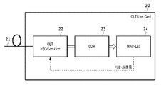
- FIG. 2 shows the configuration of a conventional receiver that inputs a reset signal from the outside.
- OLT Optical Line Terminal
- the configuration of an OLT (Optical Line Terminal) line card installed on the station side is shown.
- the CDR (Clock and Data Recovery) circuit 23 and the control LSI (MAC-LSI) 24 are connected in order.
- ONU Optical Network Unit
- the OLT Optical Line Terminal
- the OLT transceiver 22 there is a CDR circuit 23 between the OLT transceiver 22 on which the BTIA is mounted and the MAC-LSI 24, and the reset signal must be wired so as to bypass the CDR circuit 23.
- the MAC-LSI24 needs to be provided with a circuit for generating a reset signal, and needs to be integrally designed including the wiring in the line card 20, resulting in poor versatility.
- the OLT transceiver 22 is generally removable, and it is not desirable that it be an incompatible dedicated product.
- Non-Patent Document 1 the end of the burst signal is detected by counting the signal pattern immediately before the final output stage of LA (Limiting Amp). Further, a circuit for detecting the presence or absence of data is combined to change the common potential of the differential input unit of the LA during the no-signal period during the burst period.
- the BTIA generates a reset signal by detecting a change in the common potential of the differential output unit of the output buffer connected to the LA, and changes the time constant of the BTIA.
- the OLT transceiver is a removable part on the line card, and it is not desirable to be a dedicated product.
- the BTIA is also mounted on the OLT transceiver as a component integrally integrated with the PD called ROSA (Receiver Optical SubAssembly). Therefore, the method of combining the dedicated TIA and LA as in Non-Patent Document 1 lacks compatibility and is not desirable.
- a circuit for counting data signals is required in the LA, which causes problems such as increased power consumption and circuit area.
- An object of the present invention is to realize the generation of a reset signal by the TIA circuit alone.
- the present invention comprises a transimpedance stage in a transimpedance amplifier that converts a current signal into a voltage signal.
- a gain control circuit that compares the output of the transimpedance stage with a reference voltage and outputs a gain control voltage, and a reset that outputs a reset signal having a predetermined pulse width at at least one of the rise and fall of the gain control voltage. It is characterized by having a signal output circuit.
- FIG. 1 is a diagram showing a circuit configuration of a BTIA including a conventional AGC and AOC.
- FIG. 2 is a diagram showing a configuration of a conventional receiver that inputs a reset signal from the outside.
- FIG. 3 is a diagram for explaining the automatic gain control of the conventional BTIA.
- FIG. 4 is a diagram showing a circuit configuration of BTIA according to the first embodiment of the present invention.
- FIG. 5 is a diagram showing a timing chart of the BTIA of the first embodiment.
- FIG. 6 is a diagram showing a circuit configuration of BTIA according to a second embodiment of the present invention.
- FIG. 7 is a diagram showing a timing chart of the BTIA of the second embodiment.
- FIG. 8 is a diagram showing a circuit configuration of BTIA according to a third embodiment of the present invention.
- FIG. 9 is a diagram showing a circuit configuration of BTIA according to a fourth embodiment of the present invention.
- the BTIA 30 includes a PD that receives an optical signal, a transimpedance stage 31 in which the anode terminal of the PD is connected to an input terminal, an intermediate buffer 32 connected to the output terminal of the transimpedance stage 31, and an output terminal of the intermediate buffer 32.
- the output buffer 33 is provided with the output buffer 33 connected to the output buffer 33, and the output of the output buffer 33 becomes the output of the BTIA 30.
- the circuit format is often converted from single amplification to differential amplification, but this is omitted here. Also, AOC is omitted.
- the AGC 34 compares the output of the transimpedance stage 31 with the reference voltage Vref, and outputs the gain control voltage Vctto based on the comparison result.
- the gain of the transimpedance stage 31 is changed by changing the value of the feedback resistor Rf of the transimpedance stage 31 according to the gain control voltage Vctt.
- the dynamic range of the BTIA is expanded by lowering the gain when a large current signal Iin is input and increasing the gain when a small current signal Iin is input.
- Vctnt the lower the gain
- Vctnt the higher the gain.
- FIG. 4 shows the circuit configuration of the BTIA according to the first embodiment of the present invention.
- the BTIA 40 includes a PD that receives an optical signal, a transimpedance stage 41 in which the anode terminal of the PD is connected to an input terminal, an intermediate buffer 42 connected to the output terminal of the transimpedance stage 41, and an output terminal of the intermediate buffer 42.
- the output buffer 43 is provided with the output buffer 43 connected to the output buffer 43, and the output of the output buffer 43 becomes the output of the BTIA 40. Further, it is provided with an AGC 44 that compares the output of the transimpedance stage 41 with the reference voltage Vref and outputs a gain control voltage Vct, and a reset signal (Reset) output circuit.
- the reset signal output circuit is composed of a delay circuit 45 that delays the gain control voltage Vct, a NOT circuit 46 that inverts Vctt, and an AND circuit 47 that outputs the logical product of both.
- FIG. 5 shows the timing chart of the BTIA of the first embodiment.
- the AND circuit 47 has both high inputs, that is, when the output D_Vct of the delay circuit 45 is High and Vct is Low. High reset signal is output to. Therefore, a pulse having a pulse width corresponding to the delay amount of the delay circuit 45 is output only at the falling edge of Vct.
- FIG. 5 shows the timing chart at this time.
- the BTIA 40 that receives the burst optical signal outputs a predetermined gain control voltage Vctt so as to have a gain corresponding to the input current signal Iin during the burst period, but during the no-signal period. When you enter, it changes greatly (High ⁇ Low). A reset signal is output by detecting the fall of Vct.
- the reset signal When the no-signal period between the burst periods before and after is sufficiently small, if the delay amount of the delay circuit 45 is set appropriately, the reset signal also reaches the beginning of the burst period in the subsequent stage. Therefore, if the time constant is reduced when the burst period ends and the reset signal is detected, the time constant is small at the beginning of the transition from the no-signal period to the burst period again, and the AGC and AOC respond at high speed, so that the response time Can be shortened.
- the NOT circuit of the reset signal output circuit may be connected to the output D_Vctt side of the delay circuit.
- FIG. 6 shows the circuit configuration of the BTIA according to the second embodiment of the present invention.
- the BTIA 50 includes a PD that receives an optical signal, a transimpedance stage 51 in which the anode terminal of the PD is connected to an input terminal, an intermediate buffer 52 connected to the output terminal of the transimpedance stage 51, and an output terminal of the intermediate buffer 52.
- the output buffer 53 is provided with the output buffer 53 connected to the output buffer 53, and the output of the output buffer 53 becomes the output of the BTIA 50.
- it includes an AGC 54 that compares the output of the transimpedance stage 51 with the reference voltage Vref and outputs a gain control voltage Vct, and a reset signal (Reset) output circuit.
- the reset signal output circuit is composed of a delay circuit 55 that delays the gain control voltage Vct, and an XOR circuit 56 that outputs the exclusive OR of the Vct and the output of the delay circuit 55.
- FIG. 7 shows the timing chart of the BTIA of the second embodiment.
- the XOR circuit 56 outputs a high reset signal only when one of the two inputs is High. Therefore, a pulse having a pulse width corresponding to the delay amount of the delay circuit 55 is output at the falling and rising edges of Vct. Therefore, if the time constant is reduced while the reset signal is being detected, the time constant is small at the beginning of the transition from the no-signal period to the burst period again, and the response time is shortened by the AGC and AOC responding at high speed. can do.
- FIG. 8 shows the circuit configuration of the BTIA according to the third embodiment of the present invention.
- the BTIA 60 includes a PD that receives an optical signal, a transimpedance stage 61 in which the anode terminal of the PD is connected to an input terminal, an intermediate buffer 62 connected to the output terminal of the transimpedance stage 61, and an output terminal of the intermediate buffer 62.
- the output buffer 63 is provided with the output buffer 63 connected to the output buffer 63, and the output of the output buffer 63 becomes the output of the BTIA 60.
- it includes an AGC 64 that compares the output of the transimpedance stage 61 with the reference voltage Vref and outputs a gain control voltage Vct, and a reset signal (Reset) output circuit.
- the reset signal output circuit is composed of a delay circuit 65 that delays the gain control voltage Vctt, a NOT circuit 66 that inverts Vctnt, and an AND circuit 67 that outputs the logical product of both.
- the AND circuit 67 can adjust the operating point by inputting the reference voltage Vref_reset. In the above-described embodiment, the operation has been described assuming that the signal level has only two values, High / Low, for the sake of simplicity. When the resistance value of the feedback resistor Rf of the transimpedance stage 61 is continuously changed instead of being switched, it is desirable that the output of the AND circuit 67 can be continuously changed.
- the operation of the AND circuit depends on the reference voltage that determines the operating point, and when the input signal current corresponding to an arbitrary light intensity is received only by switching High / Low at the time of inputting a large signal, the reset signal is transmitted. There is a possibility of erroneous output.
- the operating point of the XOR circuit 56 in the reset signal output circuit of the second embodiment can be adjusted by inputting the reference voltage Vref_reset.
- FIG. 9 shows the circuit configuration of the BTIA according to the fourth embodiment of the present invention.
- the BTIA 70 includes a PD that receives an optical signal, a transimpedance stage 71 in which the anode terminal of the PD is connected to an input terminal, an intermediate buffer 72 connected to the output terminal of the transimpedance stage 71, and an output terminal of the intermediate buffer 72.
- the output buffer 73 is provided with the output buffer 73 connected to the output buffer 73, and the output of the output buffer 73 becomes the output of the BTIA 70.
- it includes an AGC 74 that compares the output of the transimpedance stage 71 with the reference voltage Vref and outputs a gain control voltage Vct, and a reset signal (Reset) output circuit.
- the reset signal output circuit is composed of a delay circuit 75 that delays the gain control voltage Vct, a NOT circuit 76 that inverts Vctt, and an AND circuit 77 that outputs the logical product of both.
- the operating point of the AND circuit 77 can be adjusted by inputting the reference voltage Vref_reset, as in the AND circuit 67 of the third embodiment.
- the reset signal switches the time constants of AGC74 and AOC78. For example, if the time constant is reduced when a reset signal is detected, the time constant is small at the beginning of the transition from the no-signal period to the burst period again, and AGC and AOC can respond at high speed. During the burst period, the time constant To increase the resistance to the same sign continuity.
- the no-signal period when the light receiving element receives the burst light signal is detected and a reset signal is generated to improve the high-speed response and the same code continuous resistance. Can be compatible with each other.
Landscapes
- Engineering & Computer Science (AREA)
- Power Engineering (AREA)
- Physics & Mathematics (AREA)
- Computer Hardware Design (AREA)
- Computing Systems (AREA)
- General Engineering & Computer Science (AREA)
- Mathematical Physics (AREA)
- Electromagnetism (AREA)
- Amplifiers (AREA)
- Optical Communication System (AREA)
Priority Applications (3)
| Application Number | Priority Date | Filing Date | Title |
|---|---|---|---|
| US17/604,672 US12155358B2 (en) | 2019-05-08 | 2019-05-08 | Transimpedance amplifier |
| PCT/JP2019/018458 WO2020225893A1 (ja) | 2019-05-08 | 2019-05-08 | トランスインピーダンスアンプ |
| JP2021518267A JPWO2020225893A1 (https=) | 2019-05-08 | 2019-05-08 |
Applications Claiming Priority (1)
| Application Number | Priority Date | Filing Date | Title |
|---|---|---|---|
| PCT/JP2019/018458 WO2020225893A1 (ja) | 2019-05-08 | 2019-05-08 | トランスインピーダンスアンプ |
Publications (1)
| Publication Number | Publication Date |
|---|---|
| WO2020225893A1 true WO2020225893A1 (ja) | 2020-11-12 |
Family
ID=73050823
Family Applications (1)
| Application Number | Title | Priority Date | Filing Date |
|---|---|---|---|
| PCT/JP2019/018458 Ceased WO2020225893A1 (ja) | 2019-05-08 | 2019-05-08 | トランスインピーダンスアンプ |
Country Status (3)
| Country | Link |
|---|---|
| US (1) | US12155358B2 (https=) |
| JP (1) | JPWO2020225893A1 (https=) |
| WO (1) | WO2020225893A1 (https=) |
Families Citing this family (1)
| Publication number | Priority date | Publication date | Assignee | Title |
|---|---|---|---|---|
| CN115913137A (zh) * | 2022-11-18 | 2023-04-04 | 武汉飞思灵微电子技术有限公司 | 一种集成自动复位和快速突发响应的跨阻放大器 |
Citations (8)
| Publication number | Priority date | Publication date | Assignee | Title |
|---|---|---|---|---|
| JPS5767331A (en) * | 1980-10-14 | 1982-04-23 | Toshiba Corp | Bias varying circuit |
| JPS6275639U (https=) * | 1985-10-30 | 1987-05-14 | ||
| JP2001111395A (ja) * | 1999-10-07 | 2001-04-20 | Nec Eng Ltd | 警報変化点検出回路 |
| JP2003332987A (ja) * | 2002-04-16 | 2003-11-21 | Samsung Electronics Co Ltd | バーストモード光受信機 |
| WO2008075430A1 (ja) * | 2006-12-21 | 2008-06-26 | Mitsubishi Electric Corporation | 光受信器 |
| JP2010213128A (ja) * | 2009-03-12 | 2010-09-24 | Sumitomo Electric Device Innovations Inc | 電子回路 |
| WO2012066634A1 (ja) * | 2010-11-16 | 2012-05-24 | 三菱電機株式会社 | バースト受信器 |
| WO2016035374A1 (ja) * | 2014-09-03 | 2016-03-10 | 三菱電機株式会社 | 光受信器、光終端装置および光通信システム |
Family Cites Families (6)
| Publication number | Priority date | Publication date | Assignee | Title |
|---|---|---|---|---|
| JPH098563A (ja) * | 1995-06-20 | 1997-01-10 | Nec Miyagi Ltd | 光受信前置増幅器 |
| JP2000151290A (ja) * | 1998-11-05 | 2000-05-30 | Nec Corp | 初段増幅回路 |
| JP2002164855A (ja) * | 2000-11-29 | 2002-06-07 | Oki Electric Ind Co Ltd | 光受信回路 |
| WO2006027965A1 (ja) * | 2004-09-07 | 2006-03-16 | Matsushita Electric Industrial Co., Ltd. | 受信回路及び光受信回路 |
| EP2388933A4 (en) * | 2009-01-19 | 2014-06-25 | Hitachi Ltd | TRANSIMPEDANCE AMPLIFIER AND PON SYSTEM |
| US10019872B2 (en) | 2015-07-23 | 2018-07-10 | Bally Gaming, Inc. | Gaming machine and system for redeeming an accrued attribute in subsequent gaming instances |
-
2019
- 2019-05-08 WO PCT/JP2019/018458 patent/WO2020225893A1/ja not_active Ceased
- 2019-05-08 JP JP2021518267A patent/JPWO2020225893A1/ja active Pending
- 2019-05-08 US US17/604,672 patent/US12155358B2/en active Active
Patent Citations (8)
| Publication number | Priority date | Publication date | Assignee | Title |
|---|---|---|---|---|
| JPS5767331A (en) * | 1980-10-14 | 1982-04-23 | Toshiba Corp | Bias varying circuit |
| JPS6275639U (https=) * | 1985-10-30 | 1987-05-14 | ||
| JP2001111395A (ja) * | 1999-10-07 | 2001-04-20 | Nec Eng Ltd | 警報変化点検出回路 |
| JP2003332987A (ja) * | 2002-04-16 | 2003-11-21 | Samsung Electronics Co Ltd | バーストモード光受信機 |
| WO2008075430A1 (ja) * | 2006-12-21 | 2008-06-26 | Mitsubishi Electric Corporation | 光受信器 |
| JP2010213128A (ja) * | 2009-03-12 | 2010-09-24 | Sumitomo Electric Device Innovations Inc | 電子回路 |
| WO2012066634A1 (ja) * | 2010-11-16 | 2012-05-24 | 三菱電機株式会社 | バースト受信器 |
| WO2016035374A1 (ja) * | 2014-09-03 | 2016-03-10 | 三菱電機株式会社 | 光受信器、光終端装置および光通信システム |
Also Published As
| Publication number | Publication date |
|---|---|
| US20220216841A1 (en) | 2022-07-07 |
| JPWO2020225893A1 (https=) | 2020-11-12 |
| US12155358B2 (en) | 2024-11-26 |
Similar Documents
| Publication | Publication Date | Title |
|---|---|---|
| US10003410B2 (en) | Optical receiver, optical termination device, and optical communication system | |
| JP4935422B2 (ja) | 前置増幅器およびそれを用いた光受信装置 | |
| KR100972033B1 (ko) | 전치 증폭기와 후치 증폭기가 단일로 집적된 기가비트 수동형 광 네트워크용 버스트 모드 수신기 | |
| JP4870806B2 (ja) | トランスインピーダンスアンプ | |
| JP4850919B2 (ja) | 光受信器 | |
| EP1355464B1 (en) | DC removal in an optical receiver | |
| JP5725168B2 (ja) | 検出装置、光受信装置、検出方法および光受信方法 | |
| JP5305932B2 (ja) | 前置増幅器 | |
| CN110708032A (zh) | 跨阻放大电路 | |
| WO2011099598A1 (ja) | 光信号断検出回路および光受信器 | |
| KR101544077B1 (ko) | 친국측 장치 | |
| JP5864025B2 (ja) | バースト光受信器、バースト光受信器のapdのバイアス電圧制御方法 | |
| CN114389550A (zh) | 用于接收突发光信号的跨阻抗放大电路 | |
| US11128385B2 (en) | Signal detection circuit, optical receiver, master station device, and signal detection method | |
| KR101519443B1 (ko) | 광 수신기 | |
| KR20030082074A (ko) | 버스트모드 광 수신기 | |
| JP6661057B1 (ja) | リミッティング増幅回路 | |
| JP4558829B2 (ja) | 光受信器 | |
| JP5101131B2 (ja) | 電子回路 | |
| US20250047253A1 (en) | Transimpedance amplifier | |
| WO2020225893A1 (ja) | トランスインピーダンスアンプ | |
| CN110086433A (zh) | 一种带复位信号的突发跨阻放大器 | |
| CN101783706A (zh) | 突发接收电路 | |
| JP2012085229A (ja) | Ponシステムとその局側装置及び光受信器並びに光受信方法 |
Legal Events
| Date | Code | Title | Description |
|---|---|---|---|
| 121 | Ep: the epo has been informed by wipo that ep was designated in this application |
Ref document number: 19927952 Country of ref document: EP Kind code of ref document: A1 |
|
| ENP | Entry into the national phase |
Ref document number: 2021518267 Country of ref document: JP Kind code of ref document: A |
|
| NENP | Non-entry into the national phase |
Ref country code: DE |
|
| 122 | Ep: pct application non-entry in european phase |
Ref document number: 19927952 Country of ref document: EP Kind code of ref document: A1 |