WO2020169998A1 - 電力変換装置 - Google Patents
電力変換装置 Download PDFInfo
- Publication number
- WO2020169998A1 WO2020169998A1 PCT/IB2019/000172 IB2019000172W WO2020169998A1 WO 2020169998 A1 WO2020169998 A1 WO 2020169998A1 IB 2019000172 W IB2019000172 W IB 2019000172W WO 2020169998 A1 WO2020169998 A1 WO 2020169998A1
- Authority
- WO
- WIPO (PCT)
- Prior art keywords
- smoothing capacitor
- conductor
- base portion
- conductor portion
- housing
- Prior art date
Links
Images


Classifications
-
- H—ELECTRICITY
- H05—ELECTRIC TECHNIQUES NOT OTHERWISE PROVIDED FOR
- H05K—PRINTED CIRCUITS; CASINGS OR CONSTRUCTIONAL DETAILS OF ELECTRIC APPARATUS; MANUFACTURE OF ASSEMBLAGES OF ELECTRICAL COMPONENTS
- H05K7/00—Constructional details common to different types of electric apparatus
- H05K7/20—Modifications to facilitate cooling, ventilating, or heating
- H05K7/2089—Modifications to facilitate cooling, ventilating, or heating for power electronics, e.g. for inverters for controlling motor
- H05K7/20927—Liquid coolant without phase change
-
- H—ELECTRICITY
- H02—GENERATION; CONVERSION OR DISTRIBUTION OF ELECTRIC POWER
- H02B—BOARDS, SUBSTATIONS OR SWITCHING ARRANGEMENTS FOR THE SUPPLY OR DISTRIBUTION OF ELECTRIC POWER
- H02B1/00—Frameworks, boards, panels, desks, casings; Details of substations or switching arrangements
- H02B1/26—Casings; Parts thereof or accessories therefor
- H02B1/46—Boxes; Parts thereof or accessories therefor
- H02B1/48—Mounting of devices therein
-
- H—ELECTRICITY
- H02—GENERATION; CONVERSION OR DISTRIBUTION OF ELECTRIC POWER
- H02M—APPARATUS FOR CONVERSION BETWEEN AC AND AC, BETWEEN AC AND DC, OR BETWEEN DC AND DC, AND FOR USE WITH MAINS OR SIMILAR POWER SUPPLY SYSTEMS; CONVERSION OF DC OR AC INPUT POWER INTO SURGE OUTPUT POWER; CONTROL OR REGULATION THEREOF
- H02M7/00—Conversion of ac power input into dc power output; Conversion of dc power input into ac power output
- H02M7/003—Constructional details, e.g. physical layout, assembly, wiring or busbar connections
-
- H—ELECTRICITY
- H05—ELECTRIC TECHNIQUES NOT OTHERWISE PROVIDED FOR
- H05K—PRINTED CIRCUITS; CASINGS OR CONSTRUCTIONAL DETAILS OF ELECTRIC APPARATUS; MANUFACTURE OF ASSEMBLAGES OF ELECTRICAL COMPONENTS
- H05K5/00—Casings, cabinets or drawers for electric apparatus
- H05K5/04—Metal casings
-
- H—ELECTRICITY
- H05—ELECTRIC TECHNIQUES NOT OTHERWISE PROVIDED FOR
- H05K—PRINTED CIRCUITS; CASINGS OR CONSTRUCTIONAL DETAILS OF ELECTRIC APPARATUS; MANUFACTURE OF ASSEMBLAGES OF ELECTRICAL COMPONENTS
- H05K7/00—Constructional details common to different types of electric apparatus
- H05K7/14—Mounting supporting structure in casing or on frame or rack
- H05K7/1422—Printed circuit boards receptacles, e.g. stacked structures, electronic circuit modules or box like frames
- H05K7/1427—Housings
- H05K7/1432—Housings specially adapted for power drive units or power converters
- H05K7/14329—Housings specially adapted for power drive units or power converters specially adapted for the configuration of power bus bars
Definitions
- the present invention relates to a power conversion device.
- JP2018-12457A discloses a power conversion device including an inverter, a smoothing capacitor, and a metal housing that houses the inverter and the smoothing capacitor.
- the smoothing capacitor and the inverter are connected by the conductor portion, and an insulating material is interposed between the conductor portion and the housing to ensure insulation between the conductor portion and the metal housing. ing.
- the insulating material which is a separate member, is interposed between the conductor portion and the housing, the number of components increases and the manufacturing cost increases.
- the present invention has been made in view of the above problems, and an object thereof is to provide a power conversion device capable of cost reduction and space saving while ensuring insulation between a conductor portion connected to a smoothing capacitor and a housing. To do.
- an inverter including a plurality of electric components, a smoothing capacitor that smoothes electric power, a housing that houses the inverter and the smoothing capacitor, and a first connecting the smoothing capacitor and the inverter.
- a power converter including a conductor portion is provided.
- the housing is made of a resin material and includes a base portion on which the inverter and the smoothing capacitor are mounted, and a cover portion attached to the base portion so as to cover the inverter and the smoothing capacitor.
- the first conductor portion approaches or contacts the base portion of the housing while the smoothing capacitor and the inverter are being connected.
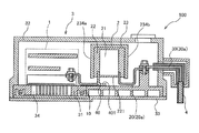
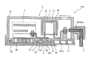
- FIG. 1 is a schematic cross-sectional view of the power conversion device according to the first embodiment.
- FIG. 2 is a schematic cross-sectional view of the power conversion device according to the first embodiment at a position different from that of FIG.
- FIG. 3 is a bottom perspective view of the smoothing capacitor.
- FIG. 4 is a cross-sectional view of the base portion of the housing before the cover portion is attached.
- FIG. 5 is an attachment diagram of the smoothing capacitor.
- FIG. 6 is a schematic cross-sectional view of the power conversion device according to the modification of the first embodiment.
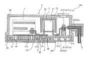
- FIG. 7 is a schematic cross-sectional view of the power conversion device according to the second embodiment.
- FIG. 8 is a bottom perspective view of the smoothing capacitor.
- FIG. 9 is a schematic sectional view of a power conversion device according to a modified example of the second embodiment.
- FIG. 10 is a schematic sectional view of the power conversion device according to the third embodiment.
- FIG. 11 is a schematic sectional view of the power conversion device according to the fourth embodiment.
- FIG. 12 is a schematic sectional view of a power conversion device according to a modification of the fourth embodiment.
- FIG. 13 is a bottom perspective view of the smoothing capacitor.
- FIG. 14 is a schematic sectional view of the power conversion device according to the fifth embodiment.
- FIG. 15 is a bottom perspective view of the smoothing capacitor.
- FIG. 16 is a schematic sectional view of the power conversion device according to the sixth embodiment.
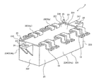
- FIG. 17 is a schematic cross-sectional view of the power converter showing the appearance of the smoothing capacitor.
- FIG. 18 is a cross-sectional schematic diagram of the power converter device of other embodiment.
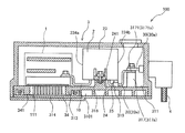
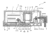
- FIG. 1 and 2 are schematic cross-sectional views of the power converter according to the first embodiment.
- FIG. 1 is a cross-sectional view of a portion including a conductor portion for input
- FIG. 2 is a cross-section of a portion including a conductor portion for output. It is a figure.
- the power conversion device 100 includes an inverter 1, a smoothing capacitor 2, and a housing 3, and is mounted on a vehicle or the like.
- the inverter 1 and the smoothing capacitor 2 are housed in the housing 3. Further, the inverter 1 and the smoothing capacitor 2 are electrically connected by a plurality of conductor portions 10 (first conductor portion), and the smoothing capacitor 2 and the power source 4 outside the housing are provided with a plurality of conductor portions 20, 30 (second conductor portion). It is electrically connected by a conductor part).
- the inverter 1 is composed of a plurality of electric components, includes a power module 11 having a built-in semiconductor element and a control board 12 having a control circuit, and has a function of converting electric power into direct current or alternating current.
- the power module 11 is configured by combining a plurality of semiconductor elements.
- the power module 11 is placed on the substrate 111 and fixed on the substrate 111 with bolts or the like.
- the substrate 111 is fixed to the base portion 31 of the housing 3 described later with bolts or the like.
- the power module 11 is electrically connected to the control board 12 and is also connected to the smoothing capacitor 2 via the conductor portion 10.
- the conductor portion 10 is fixed to the power module 11 with a bolt or the like at a terminal portion 112 provided on the power module 11.
- the smoothing capacitor 2 includes a capacitor element 21, a filling material 22, and a capacitor case 23, and is arranged side by side with the inverter 1 in a substantially horizontal direction.
- the capacitor case 23 is made of a resin such as polyphenylene sulfide (PPS) or polyphthalamide (PPA), and accommodates the capacitor element 21.
- the capacitor element 21 is connected to the power module 11 of the inverter 1 via the conductor portion 10 and also connected to the power source 4 outside the housing 3 via the conductor portions 20 and 30.
- the filling material 22 is, for example, a potting material containing silicone, fills the periphery of the capacitor element 21, and fixes the capacitor element 21 in the capacitor case 23.
- the housing 3 is provided on the lower surface of the base portion 31, the base portion 31 on which the inverter 1 and the smoothing capacitor 2 are placed, the cover portion 32 attached to the base portion 31 so as to cover the inverter 1 and the smoothing capacitor 2, It is composed of a thin plate 33 that functions as a bottom plate of the cover portion 32.
- the base portion 31 is configured as a plate-shaped member of an electrically insulating resin material such as polyphenylene sulfide (PPS) or polyphthalamide (PPA), and the inverter 1 and the smoothing capacitor 2 are mounted on the mounting surface 311.
- the base portion 31 includes a cooling path 34 (first refrigerant flow path) below a portion where the inverter 1 is mounted, through which cooling water (refrigerant) that cools the inverter 1 flows.
- a metal thin plate 33 made of aluminum or the like, which is larger than the outer shape of the lower surface 312, is provided.
- a substrate 111 having an outer shape larger than that of the cooling passage 34 is installed on the upper surface of the cooling passage 34 of the base portion 31, and the substrate 111 is fastened to the base portion 31 with a bolt or the like.
- a fin 113 is provided below the power module 11.
- the substrate 111 is provided with a plurality of holes through which the fins 113 pass, and the fins 113 are in contact with the cooling water in the cooling passage 34 through the holes.
- the power module 11 is provided with the fins 113 and brought into contact with the cooling water, the invention is not necessarily limited thereto and the fins 113 may not be provided.
- the cover part 32 is formed of a metal material such as aluminum, and is attached to the base part 31 so as to cover the periphery of the inverter 1 and the smoothing capacitor 2.
- the cover part 32 is composed of an upper wall 321 and a side wall 322.
- the side wall 322 has an opening 323 a (FIG. 1) opened so that the input conductor part 30 a connected to the power supply 4 passes through and the power supply 4 is provided.
- An opening 323b (FIG. 2) is formed so as to pass through the connecting output conductor 30b.
- a step portion 324 having an end surface that abuts on the mounting surface 311 of the base portion 31 is formed inside the side wall 322.
- the tip surface 325 of the side wall 322 abuts the outer peripheral edge 331 of the thin plate 33 provided on the lower surface 312 of the base portion 31.
- the cover portion 32, the base portion 31, and the thin plate 33 are fastened together by bolts or the like from the outside of the thin plate 33 at the portion where the step portion 324 of the cover portion 32 and the mounting surface 311 of the base portion 31 contact each other. It In this way, by completely covering the inverter 1 and the smoothing capacitor 2 with the cover portion 32 and the thin plate 33 formed of the metal material, it is possible to enhance the electromagnetic shielding property of the power conversion device 100.
- An openable/closable lid portion 326 may be provided on the upper wall 321 of the cover portion 32 so that the fastening of the conductor portion 20 and the conductor portion 30 described below can be maintained.
- FIG. 3 is a bottom perspective view of the smoothing capacitor 2.
- the capacitor case 23 of the smoothing capacitor 2 accommodates the capacitor element 21 inside, and the periphery of the capacitor element 21 is filled with the filling material 22.
- the periphery of the filler 22 is covered with the upper surface 231, the front surface 232, the rear surface 233, and the side surface 234 of the capacitor case 23.
- the bottom surface of the capacitor case 23 is open, and the filling material 22 forms a potting surface 221 on the bottom surface of the smoothing capacitor 2.
- the capacitor case 23 includes a bracket 24 protruding outward from the front surface 232 and the rear surface 233 and a positioning pin 25 protruding downward from the bottom surface.
- the bracket 24 is a member for fastening the smoothing capacitor 2 to the housing 3.
- the bracket 24 is provided with a hole portion 241 through which a bolt or the like for fastening the smoothing capacitor 2 to the base portion 31 passes.
- the positioning pin 25 is a member that determines the horizontal position of the smoothing capacitor 2 in the housing 3.
- the positioning pin 25 connects a corner portion 235 where the one side surface 234b of the capacitor case 23 on the bottom surface of the smoothing capacitor 2 connects to the front surface 232, and one side surface 234b of the capacitor case 23 on the bottom surface of the smoothing capacitor 2 connects to the rear surface 233.
- Each of the corners 236 projects downward from the bottom surface.
- the positioning pin 25 is provided at each of the corners 235 and 236 where the one side surface 234b of the capacitor case 23 on the bottom surface of the smoothing capacitor 2 is connected to the front surface 232 and the rear surface 233.
- the number and position are not limited to this. For example, it may be provided at all four corners on the bottom surface of the smoothing capacitor 2.
- a plurality of conductors 10 and 20 connected to the capacitor element 21 extend from the potting surface 221 to the outside of the smoothing capacitor 2.
- the conductor portion 10, the conductor portion 20 and the conductor portion 30 described later are metal bus bars made of, for example, copper or aluminum having good conductivity.
- the conductor portion 10 projects to the outside of the smoothing capacitor 2 from the vicinity of the one side surface 234a of the capacitor case 23 in the potting surface 221, and electrically connects the capacitor element 21 and the power module 11 of the inverter 1. Further, the conductor portion 20 projects outside the smoothing capacitor 2 from the vicinity of the other side surface 234b of the capacitor case 23 on the potting surface 221, and connects the capacitor element 21 and the power source 4 outside the power conversion device 100 via the conductor portion 30.
- the conductor portion 20 and the conductor portion 30 respectively include an input conductor portion 20a and a conductor portion 30a for inputting electric power from the power source 4, and an output conductor portion 20b and a conductor portion 30b for outputting electric power to the power source 4. ..
- the details of the arrangement of the conductors will be described later.
- FIG. 4 is a cross-sectional view of the base portion 31 of the housing 3, showing the base portion 31 before the cover portion 32 is attached.
- FIG. 5 is a cross-sectional view of the power conversion device 100, and is a mounting view of the smoothing capacitor 2.
- the base portion 31 is formed of an electrically insulating resin material, and is composed of a main body portion 313 and a bottom plate portion 314 as shown in FIG.
- the main body 313 has an opening 315 for forming the cooling passage 34, a joint 316 for joining the bottom plate 314, and a terminal 317 for fastening the conductor 20 and the conductor 30.
- the main body portion 313 further includes a holding portion 318 for holding the smoothing capacitor 2 and a pin receiving portion 319 through which the positioning pin 25 for positioning the smoothing capacitor 2 is inserted.
- the opening 315 of the main body 313 is provided in the base 31 where the inverter 1 is mounted, and the top and bottom are open.
- the joint portion 316 is a portion into which a convex portion 3141 of the bottom plate portion 314 described later is inserted and joined.
- the joint portion 316 is a hole whose lower surface is opened, and is provided around the opening portion 315.
- the bottom plate 314 has a larger outer shape than the opening 315 of the main body 313, and has a convex portion 3141 projecting upward from the upper surface of the bottom plate 314 at a position corresponding to the joint 316 of the main body 313.
- the convex portion 3141 and the joint portion 316 of the main body portion 313 are joined together by welding or the like, and the main body portion 313 and the bottom plate portion 314 are joined together to form a concave portion 341 at the position of the opening 315.
- the recess 341 is a groove for forming the cooling path 34 through which the cooling water for cooling the inverter 1 flows. As shown in FIG. 5, by covering the upper portion of the recess 341 with the substrate 111 of the power module 11, the cooling passage 34 (first refrigerant passage) surrounded by the main body portion 313, the bottom plate portion 314, and the substrate 111 is formed. It
- the terminal portion 317 of the main body portion 313 is a portion to which the conductor portion 20 connected to the smoothing capacitor 2 and the conductor portion 30 connected to the power source 4 are connected, and the smoothing capacitor 2 is installed. It is provided at a position between the location where the side wall 322 and the side wall 322 of the housing 3.
- the terminal portion 317 is integrally provided with the base portion 31 so as to project upward from the mounting surface 311 of the base portion 31, and the conductor portion 20 and the conductor portion 30 are provided on the upper surface 3171 of the terminal portion 317. It is fastened by being fastened to the base part together with bolts and the like. In this way, by providing the terminal portion 317 integrally with the base portion 31 forming the housing 3, it is possible to reduce the cost as compared with the case where the terminal portion 317 is provided as a separate member.
- the holding portion 318 of the main body portion 313 is a portion for holding the smoothing capacitor 2, and is configured to project upward from the mounting surface 311 of the base portion 31 at a position where the bracket 24 of the smoothing capacitor 2 faces. It is provided.
- the smoothing capacitor 2 is fastened to the holding portion 318 with a bolt or the like through the hole 241 of the bracket 24. Accordingly, the vertical movement of the smoothing capacitor 2 with respect to the housing 3 is restricted.
- the pin receiving portion 319 of the main body portion 313 is provided at a position corresponding to the positioning pin 25 of the smoothing capacitor 2 so as to project upward from the mounting surface 311 of the base portion 31. By inserting the positioning pin 25 into the pin receiving portion 319, the horizontal position of the smoothing capacitor 2 with respect to the housing 3 is positioned.
- the capacitor case 23 is provided with the positioning pin 25 and the base portion 31 is provided with the pin receiving portion 319 as described above, but these are not necessarily provided. ..
- a cavity 3101 having an open bottom may be formed in a portion of the base 31 where the cooling passage 34 is not provided. This reduces the weight of the power conversion device 100.
- the number and shape of the hollow portions 3101 are not particularly limited, and for example, one large hollow portion may be provided, or the bottom surface may be closed.
- the conductor portion 10 that electrically connects the inverter 1 and the smoothing capacitor 2 has one end connected to the capacitor element 21 of the smoothing capacitor 2 and downward from the potting surface 221 of the smoothing capacitor 2. Project toward.
- the other end of the conductor portion 10 is fixed to the power module 11 with a bolt or the like at a terminal portion 112 provided on the power module 11 of the inverter 1.
- the inverter 1 and the smoothing capacitor 2 are electrically connected by the conductor portion 10.
- the conductor portion 10 is close to the base portion 31 of the housing 3 while the capacitor element 21 of the smoothing capacitor 2 and the power module 11 of the inverter 1 are being connected. As described above, even if the conductor portion 10 is arranged at a position close to the base portion 31, since the base portion 31 is formed of an insulating material, the insulation between the conductor portion 10 and the housing 3 is not increased. Secured. Further, since the conductor portion 10 is close to the base portion 31, the heat of the conductor portion 10 is also dissipated by the base portion 31 via the space between the base portion 31 and the conductor portion 10. Here, since the base portion 31 includes the cooling passage 34, the base portion 31 is also cooled by the cooling water flowing through the cooling passage 34. Therefore, heat is exchanged between the base portion 31 and the conductor portion 10 cooled by the cooling water, and the smoothing capacitor 2 connected to the conductor portion 10 is cooled.
- the conductor portion 20 and the conductor portion 30 are members that electrically connect the smoothing capacitor 2 and the power source 4 outside the housing 3.
- the conductor portion 20 includes an input conductor portion 20a and an output conductor portion 20b
- the conductor portion 30 includes an input conductor portion 30a and an output conductor portion 30b.
- one end of each of the conductor portions 20 a and 20 b is connected to the capacitor element 21 of the smoothing capacitor 2 and projects downward from the potting surface 221 of the smoothing capacitor 2.
- the other ends of the conductor portions 20a and 20b are connected to the conductor portions 30a and 30b at the upper surfaces 3171a and 3171b of the terminal portions 317a and 317b protruding upward from the mounting surface 311 of the base portion 31.
- the conductor portions 20a, 20b and the conductor portions 30a, 30b are fastened together with the base portion 31 by bolts or the like on the upper surfaces 3171a, 3171b of the terminal portions 317a, 317b.
- the conductor portions 20a and 20b are close to the base portion 31 of the housing 3 while the capacitor element 21 of the smoothing capacitor 2 and the conductor portions 30a and 30b are being connected.
- the base portion 31 is formed of an insulating material
- the space between the conductor portions 20a and 20b and the housing 3 is reduced.
- the insulating property of is secured.
- the heat of the conductor portions 20a and 20b passes through the space between the base portion 31 and the conductor portions 20a and 20b. Heat is also removed to 31. That is, similar to the conductor portion 10, heat is exchanged between the base portion 31 and the conductor portions 20a and 20b cooled by the cooling water, and the smoothing capacitor 2 to which the conductor portions 20a and 20b are connected is cooled.
- each of the conductor portions 30a and 30b is connected to the conductor portions 20a and 20b on the upper surfaces 3171a and 3171b of the terminal portions 317a and 317b, and the casing portions 3a to 323b are opened through the opening portions 323a and 323b. Be extended outside.
- the other ends of the conductor portions 30a and 30b are connected to the external power source 4. In this way, the smoothing capacitor 2 and the power supply 4 are electrically connected to each other through the input conductor portion 20a and the conductor portion 30a and the output conductor portions 20b and 30b.
- the length of the portion where the conductor portion 10 and the conductor portion 20 are close to the base portion 31 is not particularly limited, but in order to further increase the cooling effect of the cooling water, it is preferable that the distance between the adjacent portions is as long as possible.
- the six conductor portions 10, two conductor portions 20a and two conductor portions 20b respectively project from the smoothing capacitor 2, but the number of conductor portions is not limited to this.
- the housing 3 is made of a resin material, and the base portion 31 on which the inverter 1 and the smoothing capacitor 2 are mounted and the cover portion 32 attached to the base portion 31 so as to cover the inverter 1 and the smoothing capacitor 2 are included. And consists of.
- the conductor portion 10 (first conductor portion) that connects the smoothing capacitor 2 and the inverter 1 is close to the base portion 31 of the housing 3 while the smoothing capacitor 2 and the inverter 1 are being connected. In this way, by forming the base portion 31 with an insulating material, the insulation between the conductor portion 10 and the housing 3 is ensured, and the conductor portion 10 is arranged at a position close to the base portion 31. ..
- the power conversion device 100 includes conductor portions 20 and 30 (second conductor portions) that connect the smoothing capacitor 2 and the power source 4 outside the housing 3, and the conductor portion 20 includes the smoothing capacitor 2 and the power source 4.
- the base portion 31 is formed of an insulating material, it is not necessary to interpose another member such as an insulating material between the conductor portion 20 and the housing 3 as in the conductor portion 10, and the cost is reduced. Is possible.
- the conductor portion 20 is arranged at a position close to the base portion 31, space can be saved as compared with the case where the insulating space distance between the conductor portion 20 and the housing 3 is increased. That is, it is possible to provide a power conversion device that is low in cost and space-saving while ensuring insulation between the conductor portion 20 connected to the smoothing capacitor 2 and the housing 3.
- the base portion 31 of the power conversion device 100 includes a cooling passage 34 (first refrigerant passage) through which cooling water (refrigerant) for cooling the inverter 1 flows.
- a cooling passage 34 first refrigerant passage
- the inverter 1 is directly cooled, and the base portion 31 is also cooled by heat exchange between the cooling water and the base portion 31.
- the conductor portions 10 and 20 are close to the base portion 31, the heat of the conductor portions 10 and 20 is also removed by the base portion 31 via the space between the base portion 31 and the conductor portions 10 and 20. Therefore, heat is exchanged between the base portion 31 and the conductor portions 10 and 20 cooled by the cooling water, and the cooling performance of the smoothing capacitor 2 to which the conductor portions 10 and 20 are connected can be improved. That is, it is possible to provide a power conversion device that improves the cooling effect of the smoothing capacitor 2 while ensuring insulation between the conductors 10 and 20 connected to the smoothing capacitor 2 and the housing 3.
- FIG. 6 is a schematic cross-sectional view of a power conversion device 100 according to a modified example of the first embodiment.
- the conductor portion 10 is arranged so as to come into contact with the base portion 31 of the housing 3 while the capacitor element 21 of the smoothing capacitor 2 and the power module 11 of the inverter 1 are being connected. To be done. As described above, even if the conductor portion 10 is brought into contact with the base portion 31, since the base portion 31 is formed of the insulating material, the insulating property between the conductor portion 10 and the housing 3 is ensured.
- the base portion 31 of the housing 3 is formed of an insulating resin material, and the conductor portion 10 (first conductor portion) that connects the smoothing capacitor 2 and the inverter 1 is the smoothing capacitor 2 and the inverter 1.
- the base portion 31 of the housing 3 is contacted during the connection between and. That is, the base portion 31 is formed of an insulating material to ensure insulation between the conductor portion 10 and the housing 3, and the conductor portion 10 is arranged so as to contact the base portion 31. Since the space between the conductor portion 10 and the housing 3 is eliminated by bringing the conductor portion 10 into contact with the housing 3 in this manner, it is possible to further save the space of the power conversion device. That is, it is possible to provide a space-saving power conversion device while ensuring insulation between the conductor portion 10 connected to the smoothing capacitor 2 and the housing 3.
- the conductor portion 10 since the conductor portion 10 is in contact with the base portion 31 of the housing 3, heat exchange is performed between the cooling water flowing through the cooling passage 34 (first refrigerant passage) and the conductor portion 10 via the base portion 31. Is done. That is, heat is exchanged between the cooling water and the conductor portion 10 without passing through the space between the conductor portion 10 and the base portion 31. Therefore, compared with the case where the conductor portion 10 is not in contact with the base portion 31 of the housing 3, the cooling effect of the cooling water flowing through the cooling passage 34 is more easily transmitted to the conductor portion 10, and the smoothing capacitor connected to the conductor portion 10 is more easily transmitted.
- the cooling performance of No. 2 can be further improved. That is, it is possible to provide a power conversion device that further improves the cooling performance of the smoothing capacitor 2 while ensuring the insulation between the housing 3 and the conductor portion 10.
- both the conductor portion 10 and the conductor portion 20 may be arranged to be in contact with the base portion 31, or only the conductor portion 20 may be arranged.
- the conductor portion 10 may be arranged so as to be in contact with the base portion 31 and be close to the base portion 31.
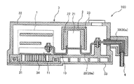
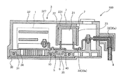
- FIG. 7 is a schematic cross-sectional view of the power conversion device 100 according to the second embodiment
- FIG. 8 is a bottom perspective view of the smoothing capacitor 2.
- the present embodiment is different from the first embodiment and the modification of the first embodiment in that a conductor portion 40 (third conductor portion) dedicated to cooling is provided.
- the smoothing capacitor 2 has a potting surface 221 formed by the filler 22 on the bottom surface. From the potting surface 221, in addition to the conductor portion 10 and the conductor portion 20, the conductor portion 40 is outside the capacitor. Be extended to.
- the conductor section 40 is a member for cooling the capacitor, and is made of, for example, copper or aluminum having good conductivity. As shown in FIG. 7, the conductor portion 40 has one end connected to the capacitor element 21 and the other end in contact with the base portion 31. Further, the conductor portion 40 projects from the vicinity of the one side surface 234 a of the capacitor case 23 on the potting surface 221 to the outside of the smoothing capacitor 2 and extends to a position where it contacts the base portion 31. The conductor portion 40 is bent at a position in contact with the base portion 31, and is extended inward of the smoothing capacitor 2 while being in contact with the base portion 31. Thereby, the contact surface 401 where the conductor portion 40 and the base portion 31 contact each other is formed.
- the conductor portion 40 contacts the base portion 31, heat is exchanged between the cooling water flowing through the cooling passage 34 and the conductor portion 40 through the base portion 31, and the conductor portion 40 and the conductor portion 40 are exchanged.
- the smoothing capacitor 2 connected to is cooled. That is, by providing the conductor portion 40 dedicated to cooling, the cooling effect of the cooling water is transmitted to the conductor portion 40 via the base portion 31, so that the cooling performance of the smoothing capacitor 2 is further improved. Further, even if the conductor portion 40 is arranged at a position in contact with the base portion 31 as described above, since the base portion 31 is made of an insulating material, the insulating property between the conductor portion 40 and the housing 3 is reduced. Is secured.
- the conductor portion 40 is bent at a position where it comes into contact with the base portion 31, and a contact surface 401 is formed between the conductor portion 40 and the base portion 31, so that the conductor portion 40 and the base portion 31 are separated from each other.
- the contact area is expanded, and the cooling performance of the smoothing capacitor 2 is further improved.
- the power conversion device 100 includes a base portion 31 of the housing 3 formed of an insulating resin material and a conductor portion 40 for cooling the smoothing capacitor 2.
- the conductor portion 40 has a portion that is connected to the smoothing capacitor 2 and that contacts the base portion 31 of the housing 3. That is, the base portion 31 is made of an insulating material to ensure insulation between the conductor portion 40 and the housing 3, and the conductor portion 40 is in contact with the base portion 31.
- heat is exchanged between the cooling water flowing through the cooling passage 34 and the conductor portion 40 via the base portion 31.
- the cooling effect of the cooling water flowing through the cooling passage 34 is transmitted to the conductor portion 40 via the base portion 31, so that the cooling performance of the smoothing capacitor 2 connected to the conductor portion 40 is further improved. Therefore, it is possible to provide a power conversion device in which the cooling effect of the smoothing capacitor 2 is further improved while ensuring the insulation between the housing 3 and the conductor portion 40.
- the conductor portion 40 be disposed in contact with the base portion 31 as in the present embodiment, but the present invention is not limited to this, and the conductor portion 40 is not limited thereto. It may be arranged at a position close to 31.
- the conductor portion 40 is bent inward of the smoothing capacitor 2, but the bending direction may be outward of the smoothing capacitor 2.
- the conductor portion 40 is provided so as to project from the vicinity of the one side surface 234a of the capacitor case 23 to the outside of the smoothing capacitor 2, but the conductor portion 40 is provided on the other side surface 234b of the capacitor case 23. You may provide so that it may protrude from the vicinity.
- the positioning pin 25 is not provided in the capacitor case 23, but the positioning pin 25 and the pin receiving portion 319 may be provided to position the smoothing capacitor 2 as in the first embodiment.
- a power converter 100 according to a modification of the second embodiment will be described with reference to FIG. 9.
- the same elements as those of the other embodiments are designated by the same reference numerals, and the description thereof will be omitted.
- FIG. 9 is a schematic cross-sectional view of a power conversion device 100 according to a modified example of the second embodiment. As shown in FIG. 9, in this modification, the conductor portion 10 (first conductor portion) and the conductor portion 40 (third conductor portion) are not in direct contact with the base portion 31, and the conductor portion 10 and the conductor portion 10 are not directly in contact with each other.
- the elastic conductive member 5 is sandwiched between 40 and the base portion 31 of the housing 3.
- the conductor portion 10 protruding from the potting surface 221 formed on the bottom surface of the smoothing capacitor 2 is close to the base portion 31 of the housing 3 while the smoothing capacitor 2 and the inverter 1 are being connected. ..
- the conductor portion 40 protruding from the potting surface 221 formed on the bottom surface of the smoothing capacitor 2 is bent inward of the smoothing capacitor 2 at a position close to the base portion 31 of the housing 3. Note that the bending direction may be the outside direction of the smoothing capacitor 2 as in the second embodiment.
- the elastic conductive member 5 is interposed between the conductor portions 10 and 40 and the base portion 31.
- the elastic conductive member 5 is, for example, highly conductive grease, an adhesive, a sheet, or the like, and is provided between the conductor portions and the base portion 31 at the portions where the conductor portions 10 and 40 and the base portion 31 are close to each other.
- the upper surface 51 of the elastic conductive member 5 contacts the conductor portions 10 and 40, and the bottom surface 52 contacts the base portion 31.
- the elastic conductive member 5 is dimensioned between the conductor portions 10 and 40 and the base portion 31. Fulfills the tolerance absorbing function.
- the heat transfer coefficient between the conductor portions 10 and 40 and the base portion 31 can be improved as compared with the case where the conductor portions 10 and 40 are brought into direct contact with the base portion 31. That is, the heat exchange rate between the cooling water flowing through the cooling passage 34 and the conductor portions 10, 40, which is performed via the base portion 31, is improved.
- the base portion 31 is formed of an insulating material. Insulation between the conductor portions 10 and 40 and the housing 3 is ensured.
- the power conversion device 100 includes a base portion 31 of the housing 3 formed of an insulating resin material, an elastic conductive member 5 that contacts the base portion 31, and a conductor portion 10 (first conductor portion) and a conductor portion 40.
- the (third conductor portion) comes into contact with the elastic conductive member 5 in the portion close to the base portion 31. That is, by forming the base portion 31 with an insulating material, the insulation between the conductor portions 10 and 40 and the housing 3 is ensured, and the conductor portions 10 and 40 are connected via the elastic conductive member 5 to the base portion 31. Is in contact with.
- the elastic conductive member 5 is The dimensional tolerance between 40 and the base portion 31 is absorbed.
- the thermal conductivity between the conductor portions 10 and 40 and the base portion 31 can be improved as compared with the case where the conductor portions 10 and 40 are brought into direct contact with the base portion 31. Therefore, the heat exchange rate between the cooling water flowing through the cooling passage 34 and the conductor portions 10 and 40 performed via the base portion 31 is improved, and the cooling performance of the smoothing capacitor 2 can be further improved. That is, it is possible to provide a power conversion device that further improves the cooling performance of the smoothing capacitor 2 while ensuring the insulation between the housing 3 and the conductor portions 10 and 40.
- the elastic conductive member 5 is interposed between the conductor portions 10 and 40 and the base portion 31 in the present embodiment, the conductor portion 20 and the base portion are provided in a portion where the conductor portion 20 and the base portion 31 are close to each other. An elastic conductive member 5 that contacts the portion 31 may be provided.
- the power converter 100 according to the third embodiment will be described with reference to FIG. 10.
- the same elements as those of the other embodiments are designated by the same reference numerals, and the description thereof will be omitted.
- FIG. 10 is a schematic cross-sectional view of the power conversion device 100 according to the third embodiment.
- the base portion 31 includes a second cooling passage 35 (second refrigerant passage) below the elastic conductive member 5 through which cooling water (refrigerant) flows.
- the main body portion 313 of the base portion 31 has a recess 351 whose bottom surface is open below the position where the conductor portions 10 and 40 face each other, that is, below the elastic conductive member 5. Further, the main body portion 313 has a joint portion 316 which is a hole whose lower surface is opened around the opening 315 and around the recess 351.
- the bottom plate portion 314 of the base portion 31 has an outer shape that is large enough to cover the bottom surfaces of both the opening 315 and the recessed portion 351 of the main body portion 313, and is located at a position corresponding to the joint portion 316.
- the convex portion 3141 and the joint portion 316 of the main body portion 313 are joined by welding or the like, and the main body portion 313 and the bottom plate portion 314 are joined, so that the main body portion 313, the bottom plate portion 314, and the power module are located at the positions of the openings 315.
- the cooling path 34 surrounded by the substrate 111 of 11 is formed.
- a second cooling passage 35 surrounded by the main body portion 313 and the bottom plate portion 314 is formed at the position of the concave portion 351.
- the cooling passage 35 is a passage through which cooling water for cooling the smoothing capacitor 2 flows, and is formed below the position where the conductor portions 10 and 40 face each other, that is, below the elastic conductive member 5, and the cooling passage 35 is formed. Connect to 34. Therefore, the cooling water circulates through the cooling passage 34 and the cooling passage 35 and flows. As described above, by providing the second cooling passage 35 below the position where the conductor portions 10 and 40 face each other, the conductor portions 10 and 40 and the cooling water can be separated from each other as compared with the case where the base portion 31 has only the cooling passage 34. The heat transfer path between them is shortened, and the cooling performance of the smoothing capacitor 2 can be further improved.
- the conductor portions 10 and 40 are in contact with the base portion 31 of the housing 3 via the elastic conductive member 5 having high conductivity, but the base portion 31 has an insulating property. Since it is formed of the above material, the insulation between the conductor portions 10 and 40 and the housing 3 is secured.
- cooling passage 34 and the cooling passage 35 are located upstream of the cooling passage 34 when it is desired to cool the inverter 1 (power module 11) more than at the smoothing capacitor 2, and when the cooling of the smoothing condenser 2 is desired. Should be on the upstream side.
- the base portion 31 of the housing 3 is formed of an insulating resin material, and the base portion 31 is below the portion facing the conductor portions 10 and 40, that is, below the elastic conductive member 5.
- a cooling passage 35 (second refrigerant passage) through which cooling water (refrigerant) flows is provided. That is, by forming the base portion 31 with an insulating material, the insulation between the conductor portions 10 and 40 and the housing 3 is secured, and below the elastic conductive member 5 with which the conductor portions 10 and 40 contact.
- a second cooling passage 35 is provided.
- the heat transfer path between the conductor portions 10 and 40 and the cooling water is shortened, and the cooling performance of the smoothing capacitor 2 is reduced as compared with the case where the base portion 31 has only the cooling passage 34 for cooling the inverter 1. Further improve. That is, it is possible to further improve the cooling performance of the smoothing capacitor 2 while ensuring the insulation between the housing 3 and the conductor portions 10 and 40.
- the elastic conductive member 5 is interposed between the conductor portions 10 and 40 and the base portion 31 in the present embodiment, the conductor portions 10 and 40 are directly connected to the base portion 31 without the elastic conductive member 5. May be contacted with.
- the cooling passage 34 and the cooling passage 35 are connected to each other, and the cooling water is circulated between the cooling passage 34 and the cooling passage 35.
- the cooling passage 34 and the cooling passage 35 are respectively provided. It is also possible to use a separate independent flow path, in which both flow paths are not connected.
- the cooling passage 35 is provided in the portion of the base portion 31 facing the conductor portions 10 and 40, but the cooling passage 35 is provided only in the position facing either the conductor portion 10 or the conductor portion 40. May be provided, or the cooling path 35 may be provided in a portion facing the conductor portion 20. Further, the cooling passage 45 may be provided in a portion of the base portion 31 facing the conductor portions 10 and 40, and another cooling passage may be provided in a portion of the base portion 31 facing the conductor portion 20.
- FIG. 11 is a schematic sectional view of the power conversion device 100 according to the fourth embodiment. As shown in FIG. 11, the present embodiment differs from the third embodiment in that the base portion 31 includes the metal member 6.
- the base portion 31 includes a cooling passage 35 (second refrigerant passage) through which cooling water for cooling the smoothing condenser 2 flows, and a metal member 6 provided at a position facing the cooling passage 35.
- the cooling path 35 has a substantially U-shaped cross-sectional shape in which a recess 352 is formed at the center of the cross section as viewed from the front.
- the metal member 6 is made of a metal material having a high thermal conductivity, such as copper or aluminum, and is provided at a position facing the cooling passage 35 directly below the elastic conductive member 5.
- the metal member 6 has a T-shape in a cross section when viewed from the front of the cooling passage 35, and projects toward the upper portion 61 having the upper surface 611 that contacts the elastic conductive member 5 and the recess 351 of the cooling passage 35. It is composed of the convex portion 62.
- the metal member 6 is integrally provided on the base portion 31 by insert molding, outsert molding by press fitting, or the like.
- the metal member 6 having high thermal conductivity is provided at a position facing the cooling path 35 so as to project toward the cooling path 35, the heat of the conductor portions 10 and 40 connected to the smoothing capacitor 2 is reduced. Can be efficiently transferred to the vicinity of the cooling path 35 via the elastic conductive member 5 and the metal member 6. Further, since the base portion 31 made of a resin material is interposed between the metal member 6 and the cooling passage 35, insulation between the metal member 6 and the housing 3 and the cooling water is ensured. Insulation between the conductor portions 10 and 40 and the housing 3 is ensured.
- the cooling passage 35 is provided in a substantially U-shaped shape in a cross section viewed from the front direction, the contact surface area between the cooling water and the base portion 31 is larger than that in the case where the round or square cooling passage is provided. Will grow. Thereby, the heat exchange rate between the cooling water and the base portion 31 is improved, and the heat exchange rate between the cooling water and the conductor portions 10 and 40 performed via the base portion 31 is also improved. Therefore, the cooling performance of the smoothing capacitor 2 connected to the conductor portions 10 and 40 is further improved.
- the base portion 31 of the housing 3 is formed of an insulating resin material
- the base portion 31 includes a metal member 6 that contacts the elastic conductive member 5, and the metal member 6 faces the cooling path 35. It is provided at the position where In this way, since the metal member 6 that contacts the elastic conductive member 5 is provided at the position facing the cooling path 35, the heat of the conductor portions 10 and 40 connected to the smoothing capacitor 2 is applied to the elastic conductive member 5 and the metal member 6. The heat can be efficiently transferred to the vicinity of the cooling path 35 via.
- the base portion 31 made of a resin material is interposed between the metal member 6 and the cooling passage 35, insulation between the metal member 6 and the housing 3 and the cooling water is ensured. Insulation between the conductor portions 10 and 40 and the housing 3 is ensured. Therefore, the cooling efficiency of the smoothing capacitor 2 can be further improved while ensuring the insulation between the conductors 10 and 40 and the housing 3.
- the metal member 6 contacting the elastic conductive member 5 also functions as a heat mass for accumulating the heat of the conductor portions 10 and 40. Therefore, since the heat capacity of the base portion 31 is increased by the metal member 6, the temperature rise of the smoothing capacitor 2 connected to the conductor portions 10 and 40 can be suppressed to a low level, and the transient thermal performance of the smoothing capacitor 2 is improved.
- the metal member 6 is provided directly below the elastic conductive member 5 that contacts the conductor portions 10 and 40. However, below the conductor portion 20, the elastic conductive member 5 and the metal that contacts the elastic conductive member 5 are provided. The member 6 and the cooling passage 35 may be provided.
- the cross section of the cooling passage 35 is formed in a substantially U shape, and the cross section of the metal member 6 is formed in a T shape in order to bring the metal member 6 closer to the cooling water.
- the shapes of the cooling passage 35 and the metal member 6 are not necessarily limited to this. If the metal member 6 contacts the elastic conductive member 5 and the base portion 31 is interposed between the metal member 6 and the cooling passage 35, the cooling passage 35 and the metal member 6 may have any shape.
- FIG. 12 is a schematic sectional view of a power conversion device 100 according to a modified example of the fourth embodiment
- FIG. 13 is a bottom perspective view of the smoothing capacitor 2.
- the base portion 31 has a protrusion 310 for positioning the smoothing capacitor 2
- the conductors 10 and 20 have holes 101, through which the protrusion 310 is inserted.
- 201 positioning hole
- the base portion 31 has a surface (mounting surface 311) on which the inverter 1 and the smoothing capacitor 2 are mounted, at positions corresponding to holes 101 and 201 of conductor portions 10 and 20 described later. It has a protruding portion 310 that protrudes.
- the protruding portion 310 is provided integrally with the base portion 31 and is inserted into the holes 101 and 201 of the conductor portions 10 and 20.
- the projecting portions 310 of the base portion 31 are inserted in locations close to the base portion 31, respectively.
- the holes 101 and 201 are provided.
- the holes 101 and 201 are provided in the conductor portion 10 and the conductor portion 20 that are arranged to face each other among the plurality of conductor portions 10 and 20, and the center point of the hole 101 of the conductor portion 10 and the conductor portion 10 face each other.
- the center point of the hole 201 of the conductor portion 20 is arranged on a straight line parallel to the front surface 232 and the rear surface 233 of the smoothing capacitor 2.
- the holes 101 and 201 are preferably provided in the conductor portion 10 and the conductor portion 20 arranged to face each other, from the viewpoint of ensuring the positioning stability of the smoothing capacitor 2, but not limited to this.
- they may be provided in the conductor portions that do not face each other, or a positioning hole may be provided in the conductor portion 40.
- the holes 101 and 201 are provided in the conductor portion 10 and the conductor portion 20, respectively, but the number of conductor portions in which the holes 101 and 201 are provided is not limited to this. You may provide a positioning hole in.
- the power conversion device 100 has a projecting portion 310 in which the base portion 31 of the housing 3 projects from the surface (mounting surface 311) on which the inverter 1 and the smoothing capacitor 2 are mounted, and projects into the conductor portions 10 and 20. Holes (positioning holes) 101 and 201 into which the portion 310 is inserted are provided. By inserting the protruding portion 310 of the base portion 31 into the holes 101 and 201 of the conductor portions 10 and 20, the smoothing capacitor 2 is positioned and the conductor portions 10 and 20 are also positioned. Since the conductors 10 and 20 are directly positioned in this way, the positioning accuracy of the conductors 10 and 20 with respect to the terminals 112 and 317 is improved, and the connection quality of the conductors in the terminals 112 and 317 is improved.
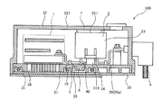
- FIG. 14 is a schematic cross-sectional view of the power conversion device 100 according to the fifth embodiment
- FIG. 15 is a bottom perspective view of the smoothing capacitor 2.
- the conductor portion 40A (third conductor portion) for cooling the smoothing capacitor 2 projects from the potting surface 221 of the smoothing capacitor 2 and faces the cooling path 35. Is different from the other embodiments in that it is inserted into the base portion 31.
- the base portion 31 is a conductor for cooling the metal member 6A having a high thermal conductivity, the cooling path 35 and the smoothing capacitor 2 which are formed in a substantially U shape in a cross section as viewed from the front. It has a groove 402 into which the portion 40A is inserted.
- the cooling passage 35 has a substantially U-shaped cross-sectional shape in which a recess 352 is formed at the center of the cross section viewed from the front direction.
- the metal member 6A is provided at a position facing the cooling passage 35 directly below the elastic conductive member 5, and has an L-shaped shape in a cross section viewed from the front direction of the cooling passage 35.
- the metal member 6A includes an upper portion 61A having an upper surface 611A that contacts the elastic conductive member 5 and a convex portion 62A that protrudes toward the concave portion 352 of the cooling passage 35.
- the convex portion 62A extends to the vicinity of the cooling passage 35, and transfers the heat of the smoothing capacitor 2 transmitted to the metal member 6A via the conductor portion 10 and the elastic conductive member 5 to the vicinity of the cooling water flowing through the cooling passage 35. .. Since the base portion 31 made of a resin material is interposed between the metal member 6A and the cooling passage 35, the insulation between the metal member 6A and the housing 3 and the cooling water is ensured. Insulation between the conductor portion 10 and the housing 3 is ensured.
- the groove 402 formed in the base portion is a groove into which the conductor portion 40A for cooling the smoothing capacitor 2 is inserted, and is formed toward the recess 352 of the cooling passage 35 up to the vicinity of the cooling passage 35.
- the conductor portion 40A is a member for cooling the capacitor, one end thereof is connected to the capacitor element 21 of the smoothing capacitor 2, and the smoothing capacitor 2 is connected from the vicinity of the one side surface 234a of the capacitor case 23 in the potting surface 221 of the smoothing capacitor 2. It projects downward to the outside.
- the other end of the conductor portion 40A is inserted into the groove 402 of the base portion 31 by light press fitting or the like.
- the conductor portion 40A is not bent, but protrudes from the potting surface 221 of the smoothing capacitor 2 and extends to the vicinity of the cooling path 35. As a result, the heat of the smoothing capacitor 2 is transferred to the vicinity of the cooling water flowing through the cooling passage 35 by the conductor portion 40A.
- the base portion 31 is formed of an insulating resin material, the insulation between the conductor portion 40A inserted into the base portion 31 and the housing 3 is ensured.
- the smoothing capacitor 2 can be positioned and the conductor portions 10 and 20 can be positioned with respect to the terminal portions 112 and 317.
- the base portion 31 of the housing 3 is formed of an insulating resin material, and the conductor portion 40A (third conductor portion) whose one end is connected to the smoothing capacitor 2 is located at a position facing the cooling path 35. At the base portion 31. As a result, the heat of the smoothing capacitor 2 is transferred to the vicinity of the cooling water flowing through the cooling passage 35 by the conductor portion 40A.
- the base portion 31 is formed of an insulating resin material, the insulation between the conductor portion 40A inserted into the base portion 31 and the housing 3 is ensured. Therefore, it is possible to further improve the cooling performance of the smoothing capacitor 2 while ensuring insulation between the conductor portion 40A and the housing 3.
- the smoothing capacitor 2 can be positioned and the conductor portions 10 and 20 can be positioned with respect to the terminal portions 112 and 317.
- the positioning accuracy of the conductor portions 10 and 20 with respect to the terminal portions 112 and 317 is improved by positioning the conductor portion 40A instead of the positioning pin 25 of the capacitor case 23, and the conductor portions of the terminal portions 112 and 317 are positioned.
- the connection quality is stable.
- the cross-sectional shape of the metal member 6A is L-shaped and the cross-sectional shape of the cooling passage 35 is substantially U-shaped, but the shape of the metal member 6A and the cooling passage 35 is not limited to this. I can't.
- the metal member 6A and the cooling passage 35 may have any shape as long as the conductor portion 40A and the one end of the metal member 6A are located near the cooling passage 35.
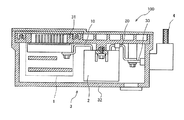
- FIG. 16 is a schematic cross-sectional view of the power converter 100 according to the sixth embodiment
- FIG. 17 is a schematic cross-sectional view of the power converter 100 showing the appearance of the smoothing capacitor 2.
- the elastic member 7 is sandwiched between the upper surface 231 of the smoothing capacitor 2 and the cover portion 32 of the housing 3, and the smoothing capacitor 2 and the housing 3 are bolted. It is different from the other embodiments in that they are not fastened.
- the elastic member 7 is sandwiched between the upper surface 231 of the smoothing capacitor 2 (capacitor case 23) and the upper portion 327 of the cover 32 of the housing 3.
- the elastic member 7 is made of an elastic material having better thermal conductivity than the capacitor case 23, and the lower surface 71 contacts the upper surface 231 of the smoothing capacitor 2 and the upper surface 72 contacts the inner surface of the upper portion 327 of the cover portion 32.
- the elastic member 7 regulates the vertical movement of the smoothing capacitor 2
- the bracket 24 of the smoothing capacitor 2 and the holding portion 318 of the base portion 31 are separated from each other. Not fastened with bolts, etc.
- the elastic member 7 may be a conductive member or an insulating member as long as it is an elastic material having good thermal conductivity.
- the upper surface 231 of the smoothing capacitor 2 is in contact with the cover portion 32 of the housing 3 via the elastic member 7.
- the vertical movement of the smoothing capacitor 2 is restricted, and it is not necessary to fasten the capacitor case 23 of the smoothing capacitor 2 and the base portion 31 of the housing 3 with a bolt or the like. Therefore, the takt time at the time of manufacturing can be shortened.
- the elastic member 7 interposed between the smoothing capacitor 2 and the cover portion 32 of the housing 3 is made of an elastic material having better thermal conductivity than the capacitor case 23. Therefore, the heat of the smoothing capacitor 2 can be dissipated from the elastic member 7 to the cover portion 32 made of a metal material, and the temperature rise of the smoothing capacitor 2 can be suppressed.
- the mounting direction of the power conversion device 100 does not necessarily need to arrange the base portion 31 of the housing 3 on the lower side, and may be freely set according to the layout of the vehicle in which the power conversion device 100 is mounted. It may be arranged in any direction.
- the power converter 100 shown in FIG. 1 and the like may be installed upside down so that the base 31 is on the top and the cover 32 is on the bottom. May be installed in a tilted state.
- the cooling water is used as the cooling medium flowing through the cooling passage, but the cooling medium is not limited to this and may be, for example, a cooling medium gas.
Abstract
複数の電気部品から構成されるインバ一夕と、電力を平滑化する平滑コンデンサと、インバ一タ及び平滑コンデンサを収容する筐体と、平滑コンデンサとインバ一夕とを接続する第1導体部と、を備える電力変換装置が提供される。筐体は、樹脂材料により形成され、インバ一タ及び平滑コンデンサを載置するベース部と、インバ一タ及び平滑コンデンサを覆うようにベース部に取り付けられるカバ一部と、から構成される。第1導体部は、平滑コンデンサとインバ一夕とを接続する途中において、筐体の前記ベース部に近接または接触する。
Description
本発明は、電力変換装置に関する。
JP2018−121457Aには、インバータと、平滑コンデンサと、インバータ及び平滑コンデンサを収容する金属筐体とを有する電力変換装置が開示されている。この電力変換装置では、平滑コンデンサとインバータとが導体部により接続され、導体部と金属筐体との間の絶縁性を確保するために、導体部と筐体との間に絶縁材を介在させている。
しかしながら、上記した電力変換装置は、導体部と筐体の間に別部材である絶縁材を介在させているため、構成部品数が多くなり、製造コストが増大する。
一方、絶縁材を用いずに、導体部と金属筐体との絶縁空間距離を大きくして絶縁性を確保することも可能であるが、この場合、大きなスペースが必要となり、装置が大型化してしまう。
本発明は、上記課題に鑑み、平滑コンデンサに接続する導体部と筐体との間の絶縁性を確保しつつ、低コスト化及び省スペース化が可能な電力変換装置を提供することを目的とする。
本発明の一態様によれば、複数の電気部品から構成されるインバータと、電力を平滑化する平滑コンデンサと、インバータ及び平滑コンデンサを収容する筐体と、平滑コンデンサとインバータとを接続する第1導体部と、を備える電力変換装置が提供される。筐体は、樹脂材料により形成され、インバータ及び平滑コンデンサを載置するベース部と、インバータ及び平滑コンデンサを覆うようにベース部に取り付けられるカバー部と、から構成される。第1導体部は、平滑コンデンサとインバータとを接続する途中において、筐体のベース部に近接または接触する。
以下、図面等を参照しながら、本発明の実施形態について説明する。
(第1実施形態)
図1~図5を参照して、本発明の第1実施形態に係る電力変換装置100について説明する。
図1~図5を参照して、本発明の第1実施形態に係る電力変換装置100について説明する。
図1及び図2は、第1実施形態による電力変換装置の断面模式図であり、図1は入力用の導体部を含む部分の断面図、図2は出力用の導体部を含む部分の断面図である。
図1及び図2に示すように、電力変換装置100は、インバータ1、平滑コンデンサ2、筐体3から構成され、車両等に搭載される。
インバータ1及び平滑コンデンサ2は筐体3に収容される。また、インバータ1と平滑コンデンサ2とは複数の導体部10(第1導体部)により電気的に接続され、平滑コンデンサ2と筐体外部の電源4とは複数の導体部20,30(第2導体部)により電気的に接続される。
インバータ1は複数の電気部品で構成され、半導体素子を内蔵するパワーモジュール11及び制御回路を備える制御基板12を備え、電力を直流または交流に変換する機能を有している。
パワーモジュール11は複数の半導体素子を組み合わせて構成される。パワーモジュール11は基板111に載置され、ボルト等により基板111上に固定される。基板111は後述する筐体3のベース部31にボルト等で固定される。また、パワーモジュール11は、制御基板12に電気的に接続するとともに、導体部10を介して平滑コンデンサ2に接続する。導体部10は、パワーモジュール11に設けられた端子部112においてボルト等によりパワーモジュール11に固定される。
平滑コンデンサ2は、コンデンサ素子21、充填材22、コンデンサケース23から構成され、インバータ1と略水平方向に並んで配置される。コンデンサケース23は、例えばポリフェニレンサルファイド(PPS)やポリフタルアミド(PPA)等の樹脂により構成され、コンデンサ素子21を収容する。コンデンサ素子21は、導体部10を介してインバータ1のパワーモジュール11に接続するとともに、導体部20及び導体部30を介して筐体3外部の電源4に接続する。充填材22は例えばシリコーン含有のポッティング材であり、コンデンサ素子21の周囲を満たし、コンデンサ素子21をコンデンサケース23内に固定する。
筐体3は、インバータ1及び平滑コンデンサ2を載置するベース部31と、インバータ1及び平滑コンデンサ2を覆うようにベース部31に取り付けられるカバー部32と、ベース部31の下面に設けられ、カバー部32の底板として機能する薄板33から構成される。
ベース部31は、例えばポリフェニレンサルファイド(PPS)やポリフタルアミド(PPA)等の電気絶縁性の樹脂材料により板状部材として構成され、載置面311にインバータ1及び平滑コンデンサ2を搭載する。ベース部31は、インバータ1を搭載した部分の下方に、インバータ1を冷却する冷却水(冷媒)が流れる冷却路34(第1冷媒流路)を備える。ベース部31の下面312には、下面312の外形よりも大きいアルミニウム等からなる金属製の薄板33が設けられる。
ベース部31の冷却路34の上面には、冷却路34よりも大きな外形を有する基板111が設置され、基板111はボルト等によりベース部31に締結される。パワーモジュール11の下部にはフィン113が設けられる。基板111にはフィン113を通す複数の孔が設けられ、フィン113は孔を通して冷却路34内の冷却水に接触している。なお、パワーモジュール11にはフィン113を設けて冷却水に接触させることが好ましいが、必ずしもこれに限られず、フィン113を設けていなくてもよい。
カバー部32は、例えばアルミニウム等の金属材料により形成され、インバータ1及び平滑コンデンサ2の周囲を覆うようにベース部31に取り付けられる。カバー部32は、上壁321及び側壁322から構成され、側壁322には、電源4に接続する入力用の導体部30aが通るように開口された開口部323a(図1)及び、電源4に接続する出力用の導体部30bが通るように開口された開口部323b(図2)が形成される。また、側壁322の内側部位には、ベース部31の載置面311に当接する端面を有する段部324が形成される。側壁322の先端面325は、ベース部31の下面312に設けられた薄板33の外周縁331に当接する。カバー部32、ベース部31及び薄板33は、カバー部32の段部324とベース部31の載置面311とが当接する部分において薄板33の外側からボルト等により共締めされることにより締結される。このようにして、金属材料により形成されたカバー部32と薄板33とによってインバータ1及び平滑コンデンサ2を完全に覆うことで、電力変換装置100の電磁シールド性を高めることができる。なお、カバー部32の上壁321に、開閉可能な蓋部326を設けて、後述する導体部20と導体部30との締結をメンテナンスできるようにしてもよい。
図3は平滑コンデンサ2の底面斜視図である。
平滑コンデンサ2のコンデンサケース23は内部にコンデンサ素子21を収容し、コンデンサ素子21の周囲は充填材22で満たされている。充填材22の周囲は、コンデンサケース23の上面231、前面232、後面233、及び側面234により覆われている。コンデンサケース23の底面は開口し、平滑コンデンサ2の底面において充填材22がポッティング面221を形成する。
また、コンデンサケース23は、前面232及び後面233から外側方向に突出するブラケット24及び底面から下方に突出する位置決めピン25を備える。ブラケット24は平滑コンデンサ2を筐体3に締結するための部材である。ブラケット24には、平滑コンデンサ2をベース部31に締結するためのボルト等が通る穴部241が設けられる。位置決めピン25は、筐体3内における平滑コンデンサ2の水平方向の位置を決定する部材である。位置決めピン25は、平滑コンデンサ2の底面におけるコンデンサケース23の一方側側面234bと前面232が接続する角部235、及び平滑コンデンサ2の底面におけるコンデンサケース23の一方側側面234bと後面233が接続する角部236からそれぞれ底面の下方に向かって突出する。位置決めピン25がベース部31に挿通されることで、平滑コンデンサ2の筐体3に対する水平方向の位置が位置決めされる。
なお、本実施形態では、位置決めピン25は、平滑コンデンサ2の底面におけるコンデンサケース23の一方側側面234bと前面232及び後面233が接続する角部235,236にそれぞれ設けられるが、位置決めピン25の個数及び位置はこれに限らない。例えば平滑コンデンサ2の底面における4つの角部すべてに設けても良い。
ポッティング面221からは、コンデンサ素子21に接続する複数の導体部10及び導体部20が平滑コンデンサ2の外部へと延在される。導体部10、導体部20及び後述する導体部30は、例えば導電性の良い銅やアルミニウム等で構成された金属バスバーである。導体部10は、ポッティング面221におけるコンデンサケース23の一方側側面234aの近傍から平滑コンデンサ2の外部に突出し、コンデンサ素子21とインバータ1のパワーモジュール11とを電気的に接続する。また、導体部20は、ポッティング面221におけるコンデンサケース23の他方側側面234bの近傍から平滑コンデンサ2の外部に突出し、導体部30を介してコンデンサ素子21と電力変換装置100外部の電源4とを電気的に接続する。導体部20及び導体部30は、それぞれ電源4からの電力を入力する入力用の導体部20a及び導体部30aと、電源4に電力を出力する出力用の導体部20b及び導体部30bとを備える。なお、導体部の配置の詳細については後述する。
図4は筐体3のベース部31の断面図であり、カバー部32が取り付けられる前のベース部31を示す図である。また、図5は電力変換装置100の断面図であり、平滑コンデンサ2の取付図である。
ベース部31は電気絶縁性の樹脂材料により形成され、図4に示すように、本体部313及び底板部314から構成される。本体部313は、冷却路34を形成するための開口部315、底板部314を接合するための接合部316、導体部20と導体部30とを締結するための端子部317を有する。また、図5に示すように、本体部313はさらに、平滑コンデンサ2を保持するための保持部318及び平滑コンデンサ2を位置決めする位置決めピン25が挿通されるピン受け部319を有する。
本体部313の開口部315は、ベース部31におけるインバータ1を載置する箇所に設けられ、上面及び底面が開口している。接合部316は、後述する底板部314の凸部3141が挿通され接合される部分である。接合部316は下面が開口した孔であり、開口部315の周りに設けられる。
底板部314は、本体部313の開口部315よりも大きな外形を有するとともに、本体部313の接合部316に対応する位置に底板部314の上面から上方に突出する凸部3141を有する。凸部3141と本体部313の接合部316とは、溶着等により接合され、本体部313と底板部314とが接合されることにより、開口部315の位置に凹部341が形成される。凹部341は、インバータ1を冷却する冷却水を流す冷却路34を構成するための溝である。図5に示すように、凹部341の上部をパワーモジュール11の基板111により覆うことで、本体部313、底板部314及び基板111に囲まれた冷却路34(第1冷媒流路)が形成される。
図5に示すように、本体部313の端子部317は、平滑コンデンサ2に接続する導体部20と、電源4に接続する導体部30とが接続される部分であり、平滑コンデンサ2が設置される箇所と筐体3の側壁322との間の位置に設けられる。端子部317は、ベース部31の載置面311から上方に向かって突出するようにベース部31と一体的に設けられ、導体部20と導体部30とは、端子部317の上面3171において、ボルト等によりベース部に共締めされることで締結される。このように、筐体3を構成するベース部31と一体的に端子部317を設けることで、端子部317を別部材として設ける場合に比べコストダウンを図ることができる。
本体部313の保持部318は、平滑コンデンサ2を保持するための部分であり、平滑コンデンサ2のブラケット24が対向する位置に、ベース部31の載置面311から上方に向かって突出するように設けられる。平滑コンデンサ2は、ブラケット24の穴部241を介してボルト等により保持部318に締結される。これにより、特に筐体3に対する平滑コンデンサ2の上下方向の動きが規制される。
本体部313のピン受け部319は、平滑コンデンサ2の位置決めピン25に対応する位置に、ベース部31の載置面311から上方に向かって突出するように設けられる。ピン受け部319に位置決めピン25が挿通されることで、筐体3に対する平滑コンデンサ2の水平方向の位置が位置決めされる。
なお、平滑コンデンサ2の位置決めを容易にするために、上記のようにコンデンサケース23に位置決めピン25を、ベース部31にピン受け部319をそれぞれ設けることが好ましいが、これらは必ずしも設ける必要はない。
ベース部31の冷却路34を設けない部分には、底面が開放された空洞部3101を形成してもよい。これにより、電力変換装置100が軽量化される。なお、空洞部3101の個数や形状は特に限定されず、例えば大きな空洞部を一つ設けてもよく、また底面が閉じられた構造であってもよい。
次に導体部の配置の詳細について説明する。
図1及び図2に示すように、インバータ1と平滑コンデンサ2とを電気的に接続する導体部10は、一端が平滑コンデンサ2のコンデンサ素子21に接続し、平滑コンデンサ2のポッティング面221から下方に向かって突出する。導体部10の他端はインバータ1のパワーモジュール11に設けられた端子部112において、ボルト等によりパワーモジュール11に固定される。これにより、インバータ1と平滑コンデンサ2とは、導体部10により電気的に接続される。
また、導体部10は、平滑コンデンサ2のコンデンサ素子21とインバータ1のパワーモジュール11とを接続する途中において、筐体3のベース部31に近接する。このように、導体部10をベース部31に近接する位置に配置しても、ベース部31は絶縁性の材料により形成されているため、導体部10と筐体3との間の絶縁性は確保される。また、導体部10はベース部31に近接するため、導体部10の熱はベース部31と導体部10の間の空間を介してベース部31にも抜熱される。ここで、ベース部31は冷却路34を備えるため、冷却路34を流れる冷却水により、ベース部31も冷却されている。従って、冷却水により冷却されたベース部31と導体部10との間で熱交換がされ、導体部10が接続する平滑コンデンサ2が冷却される。
導体部20及び導体部30は、平滑コンデンサ2と筐体3の外部の電源4とを電気的に接続する部材である。導体部20は、入力用の導体部20a及び出力用の導体部20bから構成され、導体部30は入力用の導体部30a及び出力用の導体部30bから構成される。図1~図3に示すように、導体部20a,20bは、一端が平滑コンデンサ2のコンデンサ素子21に接続し、平滑コンデンサ2のポッティング面221から下方に向かって突出する。導体部20a,20bの他端は、ベース部31の載置面311から上方に向かって突出する端子部317a,317bの上面3171a,3171bにおいて、導体部30a,30bに接続する。導体部20a,20bと導体部30a,30bとは、端子部317a,317bの上面3171a,3171bにおいて、ボルト等によりベース部31に共締めされる。
また、導体部20a,20bは、平滑コンデンサ2のコンデンサ素子21と導体部30a,30bとを接続する途中において、筐体3のベース部31に近接する。このように、導体部20a,20bをベース部31に近接する位置に配置しても、ベース部31は絶縁性の材料により形成されているため、導体部20a,20bと筐体3との間の絶縁性は確保される。また、導体部10と同様に、導体部20a,20bはベース部31に近接するため、導体部20a,20bの熱はベース部31と導体部20a,20bとの間の空間を介してベース部31にも抜熱される。即ち導体部10と同様に、冷却水により冷却されたベース部31と導体部20a,20bとの間で熱交換がされ、導体部20a,20bが接続する平滑コンデンサ2が冷却される。
導体部30a,30bは、一端が端子部317a,317bの上面3171a,3171bにおいて導体部20a,20bに接続されるとともに、筐体3の側壁322に形成された開口部323a,323bから筐体3の外部に延設される。導体部30a,30bの他端は外部の電源4に接続される。このように平滑コンデンサ2と電源4とは、入力用の導体部20aと導体部30a、及び出力用の導体部20bと30bを介して電気的に接続される。
なお、導体部10及び導体部20がベース部31に近接する部分の長さは特に限定されないが、冷却水による冷却効果をより大きくするために、近接する部分の距離はできるだけ長い方が好ましい。
また、図3では、6つの導体部10、それぞれ2つの導体部20a及び導体部20bが平滑コンデンサ2から突出しているが、導体部の個数はこれに限らない。
上記した第1実施形態の電力変換装置100によれば、以下の効果を得ることができる。
電力変換装置100は、筐体3が樹脂材料により形成され、インバータ1及び平滑コンデンサ2を載置するベース部31と、インバータ1及び平滑コンデンサ2を覆うようにベース部31に取り付けられるカバー部32と、から構成される。そして、平滑コンデンサ2とインバータ1とを接続する導体部10(第1導体部)は、平滑コンデンサ2とインバータ1とを接続する途中において、筐体3のベース部31に近接する。このように、ベース部31を絶縁性の材料により形成することで導体部10と筐体3との間の絶縁性を確保し、導体部10はベース部31に近接する位置に配置している。従って、導体部10と筐体3との間に絶縁材等の別部材を介在させる必要がないため低コスト化が可能となり、且つ導体部10をベース部31に近接する位置に配置しているため、導体部10と筐体3との絶縁空間距離を大きくする場合に比べ省スペース化が可能となる。即ち、平滑コンデンサ2に接続する導体部10と筐体3との間の絶縁性を確保しつつ、低コスト化及び省スペース化された電力変換装置を提供することができる。
次に、電力変換装置100は、平滑コンデンサ2と筐体3の外部の電源4とを接続する導体部20,30(第2導体部)を備え、導体部20は、平滑コンデンサ2と電源4とを接続する途中において、筐体3のベース部31に近接する。ベース部31は絶縁性の材料により形成されているため、導体部10と同様に、導体部20と筐体3との間においても絶縁材等の別部材を介在させる必要がなく、低コスト化が可能となる。また、導体部20をベース部31に近接する位置に配置しているため、導体部20と筐体3との絶縁空間距離を大きくする場合に比べ省スペース化が可能となる。即ち、平滑コンデンサ2に接続する導体部20と筐体3との間の絶縁性を確保しつつ、低コスト化及び省スペース化された電力変換装置を提供することができる。
また、電力変換装置100のベース部31は、インバータ1を冷却する冷却水(冷媒)が流れる冷却路34(第1冷媒流路)を備える。これによりインバータ1が直接冷却されるとともに、冷却水とベース部31との間の熱交換によりベース部31も冷却される。一方、導体部10,20はベース部31に近接するため、導体部10,20の熱はベース部31と導体部10,20との間の空間を介してベース部31にも抜熱される。従って、冷却水により冷却されたベース部31と導体部10,20との間で熱交換がされ、導体部10,20が接続する平滑コンデンサ2の冷却性能を向上させることができる。即ち、平滑コンデンサ2に接続する導体部10,20と筐体3との間の絶縁性を確保しつつ、平滑コンデンサ2の冷却効果を向上させた電力変換装置を提供することができる。
(第1実施形態の変形例)
図6を参照して、本発明の第1実施形態に係る電力変換装置100の変形例について説明する。
図6を参照して、本発明の第1実施形態に係る電力変換装置100の変形例について説明する。
図6は、第1実施形態の変形例による電力変換装置100の断面模式図である。図6に示すように、本変形例では、導体部10が平滑コンデンサ2のコンデンサ素子21とインバータ1のパワーモジュール11とを接続する途中において、筐体3のベース部31に接触するように配置される。このように、導体部10をベース部31に接触させても、ベース部31は絶縁性の材料により形成されているため、導体部10と筐体3との間の絶縁性は確保される。
上記した第1実施形態の変形例によれば、さらに以下の効果を得ることができる。
電力変換装置100は、筐体3のベース部31を絶縁性の樹脂材料により形成し、平滑コンデンサ2とインバータ1とを接続する導体部10(第1導体部)は、平滑コンデンサ2とインバータ1とを接続する途中において、筐体3のベース部31に接触する。即ち、ベース部31を絶縁性の材料により形成することで導体部10と筐体3との間の絶縁性を確保し、導体部10はベース部31に接触するように配置している。このように導体部10を筐体3に接触させることで導体部10と筐体3の間の空間をなくしているため、電力変換装置をより省スペース化することができる。即ち、平滑コンデンサ2に接続する導体部10と筐体3との間の絶縁性を確保しつつ、より省スペース化された電力変換装置を提供することができる。
また、導体部10が筐体3のベース部31に接触しているため、ベース部31を介して冷却路34(第1冷媒流路)を流れる冷却水と導体部10との間で熱交換が行われる。即ち、導体部10とベース部31との間の空間を介することなく冷却水と導体部10との間の熱交換が行われる。従って、導体部10が筐体3のベース部31に接触していない場合に比べ、冷却路34を流れる冷却水による冷却効果がより導体部10に伝わりやすく、導体部10に接続される平滑コンデンサ2の冷却性能をより向上することができる。即ち、筐体3と導体部10との間の絶縁性を確保しつつ平滑コンデンサ2の冷却性能をより向上させた電力変換装置を提供することができる。
なお、本実施形態では、導体部10のみをベース部31に接触させているが、導体部10及び導体部20のいずれもベース部31に接触させる配置にしてもよく、また導体部20のみをベース部31に接触させ、導体部10はベース部31に近接させるように配置してもよい。
(第2実施形態)
図7及び図8を参照して、第2実施形態による電力変換装置100を説明する。なお、第1実施形態と同様の要素には同一の符号を付し、その説明を省略する。
図7及び図8を参照して、第2実施形態による電力変換装置100を説明する。なお、第1実施形態と同様の要素には同一の符号を付し、その説明を省略する。
図7は第2実施形態による電力変換装置100の断面模式図であり、図8は平滑コンデンサ2の底面斜視図である。図7及び図8に示すように、本実施形態では、冷却専用の導体部40(第3導体部)を設けた点が第1実施形態及び第1実施形態の変形例と異なる。
図8に示すように、平滑コンデンサ2は底面に充填材22により形成されるポッティング面221を有し、ポッティング面221からは、導体部10及び導体部20に加えて導体部40がコンデンサの外部に延在される。
導体部40は、コンデンサを冷却するための部材であり、例えば導電性の良い銅やアルミニウム等で構成される。図7に示すように、導体部40は一端がコンデンサ素子21に接続し、他端はベース部31に接触する。また、導体部40は、ポッティング面221におけるコンデンサケース23の一方側側面234aの近傍から平滑コンデンサ2の外部に突出し、ベース部31に接触する位置まで延設される。ベース部31に接する位置において、導体部40は曲げ加工がされ、ベース部31に接触したまま平滑コンデンサ2の内側方向に延設される。これにより、導体部40とベース部31とが接触する接触面401が形成される。
このように、導体部40はベース部31と接触するため、ベース部31を介して冷却路34を流れる冷却水と導体部40との間で熱交換が行われ、導体部40及び導体部40に接続する平滑コンデンサ2が冷却される。即ち、冷却専用の導体部40を設けることで、冷却水による冷却効果がベース部31を介して導体部40に伝わるため、平滑コンデンサ2の冷却性能がより向上される。また、このように導体部40をベース部31に接触する位置に配置しても、ベース部31は絶縁性の材料により形成されているため、導体部40と筐体3との間の絶縁性は確保される。
また、導体部40はベース部31と接触する位置において曲げ加工が施され、導体部40とベース部31との間には接触面401が形成されるため、導体部40とベース部31との接触面積が拡大され、平滑コンデンサ2の冷却性能はさらに向上される。
上記した第2実施形態による電力変換装置100によれば、以下の効果を得ることができる。
電力変換装置100は、筐体3のベース部31を絶縁性の樹脂材料により形成するとともに、平滑コンデンサ2を冷却するための導体部40を備える。導体部40は、平滑コンデンサ2に接続するとともに、筐体3のベース部31に接触する部分を有する。即ち、ベース部31を絶縁性の材料により形成することで導体部40と筐体3との間の絶縁性を確保し、導体部40はベース部31に接触させている。これにより、ベース部31を介して冷却路34を流れる冷却水と導体部40との間で熱交換が行われる。このように、冷却路34流れる冷却水による冷却効果がベース部31を介して導体部40に伝わるため、導体部40に接続される平滑コンデンサ2の冷却性能がより向上される。従って、筐体3と導体部40との絶縁性を確保しつつ平滑コンデンサ2の冷却効果がより向上した電力変換装置を提供することができる。
なお、平滑コンデンサ2の冷却性能をより高めるために、導体部40は本実施形態のようにベース部31に接触させて配置するのが好ましいが、必ずしもこれに限られず、導体部40をベース部31に近接する位置に配置してもよい。
また、本実施形態では、導体部40は平滑コンデンサ2の内側方向に曲げ加工が施されているが、曲げ加工の方向は平滑コンデンサ2の外側方向であってもよい。
また、本実施形態では、導体部40はコンデンサケース23の一方側側面234aの近傍から平滑コンデンサ2の外部に突出するように設けているが、導体部40をコンデンサケース23の他方側側面234bの近傍から突出するように設けてもよい。
また、図8では、コンデンサケース23に位置決めピン25を設けていないが、第1実施形態のように位置決めピン25及びピン受け部319を設けて平滑コンデンサ2の位置決めを行ってもよい。
(第2実施形態の変形例)
図9を参照して、第2実施形態の変形例による電力変換装置100を説明する。なお、他の実施形態と同様の要素には同一の符号を付し、その説明を省略する。
図9を参照して、第2実施形態の変形例による電力変換装置100を説明する。なお、他の実施形態と同様の要素には同一の符号を付し、その説明を省略する。
図9は第2実施形態の変形例による電力変換装置100の断面模式図である。図9に示すように、本変形例では、導体部10(第1導体部)及び導体部40(第3導体部)とベース部31とは直接には接触せず、導体部10及び導体部40と筐体3のベース部31との間に弾性導電部材5が挟まれている。
図9に示すように、平滑コンデンサ2の底面に形成されるポッティング面221から突出する導体部10は、平滑コンデンサ2とインバータ1とを接続する途中において、筐体3のベース部31に近接する。また、平滑コンデンサ2の底面に形成されるポッティング面221から突出する導体部40は、筐体3のベース部31に近接する位置で平滑コンデンサ2の内側方向に曲げ加工が施されている。なお、第2実施形態と同様に、曲げ加工の方向は平滑コンデンサ2の外側方向であってもよい。
また、図9に示すように、導体部10,40とベース部31との間には、弾性導電部材5が介在している。弾性導電部材5は、例えば導電性の高いグリス、接着剤、シート等であり、導体部10,40とベース部31とが近接する部分において、各導体部とベース部31との間にそれぞれ設けられる。弾性導電部材5の上表面51は導体部10,40に接触し、底面52はベース部31に接触する。
このように、導電性の高い弾性導電部材5を導体部10,40とベース部31との間に介在させることにより、弾性導電部材5は導体部10,40とベース部31との間の寸法の公差吸収機能を果たす。これにより、導体部10,40をベース部31に直接接触させる場合に比べ、導体部10,40とベース部31との間の熱伝達率を向上させることができる。即ち、ベース部31を介して行われる冷却路34を流れる冷却水と導体部10,40との間の熱交換率が向上する。また、このように導体部10,40を導電性の高い弾性導電部材5を介して筐体3のベース部31に接触させていても、ベース部31は絶縁性の材料により形成されているため、導体部10,40と筐体3との間の絶縁性は確保される。
上記した第2実施形態の変形例によれば、さらに以下の効果を得ることができる。
電力変換装置100は、筐体3のベース部31を絶縁性の樹脂材料により形成するとともに、ベース部31に接触する弾性導電部材5を備え、導体部10(第1導体部)及び導体部40(第3導体部)はベース部31に近接する部分において弾性導電部材5に接触する。即ち、ベース部31を絶縁性の材料により形成することで導体部10,40と筐体3との間の絶縁性を確保し、導体部10,40は弾性導電部材5を介してベース部31に接触させている。このように、導体部10,40とベース部31とが近接する部分に、ベース部31及び導体部10,40に接触する弾性導電部材5を設けることで、弾性導電部材5は導体部10,40とベース部31との間の寸法の公差吸収機能を果たす。これにより、導体部10,40をベース部31に直接接触させる場合に比べ、導体部10,40とベース部31との間の熱伝導率を向上させることができる。従って、ベース部31を介して行われる冷却路34を流れる冷却水と導体部10,40との間の熱交換率が向上し、平滑コンデンサ2の冷却性能をさらに向上させることができる。即ち、筐体3と導体部10,40との間の絶縁性を確保しつつ平滑コンデンサ2の冷却性能をさらに向上させた電力変換装置を提供することができる。
なお、本実施形態では、導体部10,40とベース部31との間に弾性導電部材5を介在させているが、導体部20とベース部31とが近接する部分に、導体部20及びベース部31に接触する弾性導電部材5を設けてもよい。
(第3実施形態)
図10を参照して、第3実施形態による電力変換装置100を説明する。なお、他の実施形態と同様の要素には同一の符号を付し、その説明を省略する。
図10を参照して、第3実施形態による電力変換装置100を説明する。なお、他の実施形態と同様の要素には同一の符号を付し、その説明を省略する。
図10は第3実施形態による電力変換装置100の断面模式図である。図10に示すように、本実施形態では、ベース部31が、弾性導電部材5の下方に冷却水(冷媒)が流れる第2の冷却路35(第2冷媒流路)を備える。
図10に示すように、ベース部31の本体部313は、導体部10,40が対向する位置の下方、即ち、弾性導電部材5の下方に底面が開口した凹部351を有する。また、本体部313は、開口部315の周り及び凹部351の周りに下面が開口した孔である接合部316を有する。
また、ベース部31の底板部314は、本体部313の開口部315及び凹部351のいずれの底面も覆うことができる大きさの外形を有するとともに、接合部316に対応する位置に、底板部314の上面から上方に突出する凸部3141を有する。凸部3141と本体部313の接合部316とは溶着等により接合され、本体部313と底板部314とが接合されることにより、開口部315の位置に本体部313、底板部314及びパワーモジュール11の基板111により囲まれる冷却路34が形成される。また、凹部351の位置に本体部313及び底板部314により囲まれる第2の冷却路35が形成される。
冷却路35は平滑コンデンサ2を冷却するための冷却水が流れる流路であって、導体部10,40が対向する位置の下方、即ち、弾性導電部材5の下方に形成されるとともに、冷却路34に接続する。従って、冷却水は、冷却路34と冷却路35とを循環して流れる。このように、導体部10,40が対向する位置の下方に第2の冷却路35を設けることで、ベース部31が冷却路34のみを有する場合に比べ、導体部10,40と冷却水との間の伝熱経路が短縮され、平滑コンデンサ2の冷却性能をさらに向上させることができる。また、第2実施形態の変形例と同様に、導体部10,40は導電性の高い弾性導電部材5を介して筐体3のベース部31に接触させているが、ベース部31は絶縁性の材料により形成されているため、導体部10,40と筐体3との間の絶縁性は確保される。
なお、冷却路34と冷却路35とは、平滑コンデンサ2よりもインバータ1(パワーモジュール11)をより冷却したい場合は冷却路34を上流側に、平滑コンデンサ2をより冷却したい場合は冷却路35を上流側にすればよい。
上記した第3実施形態による電力変換装置100によれば、以下の効果を得ることができる。
電力変換装置100は、筐体3のベース部31を絶縁性の樹脂材料により形成するとともに、ベース部31は、導体部10、40に対向する部分の下方、即ち、弾性導電部材5の下方に冷却水(冷媒)が流れる冷却路35(第2冷媒流路)を備える。即ち、ベース部31を絶縁性の材料により形成することで導体部10,40と筐体3との間の絶縁性を確保し、導体部10,40が接触する弾性導電部材5の下方には第2の冷却路35を設けている。これにより、ベース部31がインバータ1を冷却するための冷却路34のみを有する場合に比べ、導体部10,40と冷却水との間の伝熱経路が短縮され、平滑コンデンサ2の冷却性能はさらに向上する。即ち、筐体3と導体部10,40との絶縁性を確保しつつ平滑コンデンサ2の冷却性能をさらに向上させることができる。
なお、本実施形態では、導体部10,40とベース部31との間に弾性導電部材5を介在させているが、弾性導電部材5を介在させずに導体部10,40を直接ベース部31に接触させてもよい。
また、本実施形態では、冷却路34と冷却路35とが接続し、冷却水が冷却路34と冷却路35との間で循環する構成としたが、冷却路34と冷却路35とをそれぞれ独立した別の流路にして、両流路が接続しない構成にしてもよい。
また、本実施形態では、ベース部31の導体部10,40に対向する部分に冷却路35を設けているが、導体部10または導体部40のいずれか一方に対向する位置のみに冷却路35を設けてもよく、また、導体部20に対向する部分に冷却路35を設けてもよい。また、ベース部31の導体部10,40に対向する部分に冷却路45を、導体部20に対向する部分にさらに別の冷却路を設ける構成であってもよい。
(第4実施形態)
図11を参照して、第4実施形態による電力変換装置100を説明する。なお、他の実施形態と同様の要素には同一の符号を付し、その説明を省略する。
図11を参照して、第4実施形態による電力変換装置100を説明する。なお、他の実施形態と同様の要素には同一の符号を付し、その説明を省略する。
図11は第4実施形態による電力変換装置100の断面模式図である。図11に示すように、本実施形態では、ベース部31が金属部材6を備える点が第3実施形態と異なる。
図11に示すように、ベース部31は、平滑コンデンサ2を冷却する冷却水が流れる冷却路35(第2冷媒流路)及び冷却路35に対向する位置に設けられる金属部材6を備える。冷却路35は、正面方向から見た断面の中央に凹部352が形成された略U字型の断面形状を有する。
金属部材6は、例えば銅やアルミニウム等の熱伝導率の高い金属材料で構成され、弾性導電部材5直下の冷却路35に対向する位置に設けられる。金属部材6は、冷却路35の正面方向から見た断面においてT字型の形状を有し、弾性導電部材5に接触する上面611を有する上部61及び冷却路35の凹部351に向かって突出する凸部62から構成される。金属部材6は、インサート成形や圧入によるアウトサート成形等により、ベース部31に一体化して設けられる。
このように熱伝導率の高い金属部材6を、冷却路35に対向する位置に、冷却路35に向かって突出するように設けているため、平滑コンデンサ2に接続する導体部10,40の熱を弾性導電部材5及び金属部材6を介して冷却路35の近傍まで効率良く伝熱することができる。また、金属部材6と冷却路35との間には、樹脂材料により形成されるベース部31が介在しているため、金属部材6と筐体3及び冷却水との間の絶縁性が確保され、導体部10,40と筐体3との絶縁性が確保される。
また、冷却路35は正面方向から見た断面において略U字型の形状に設けられているため、丸形や四角形の冷却路を設けた場合に比べ、冷却水とベース部31との接触表面積が大きくなる。これにより、冷却水とベース部31との間の熱交換率が向上し、ベース部31を介して行われる冷却水と導体部10,40との間の熱交換率も向上する。従って、導体部10,40に接続される平滑コンデンサ2の冷却性能がさらに向上する。
上記した第4実施形態による電力変換装置100によれば、以下の効果を得ることができる。
電力変換装置100は、筐体3のベース部31を絶縁性の樹脂材料により形成するとともに、ベース部31は弾性導電部材5に接触する金属部材6を備え、金属部材6は冷却路35に対向する位置に設けられる。このように、弾性導電部材5に接触する金属部材6を冷却路35に対向する位置に設けているため、平滑コンデンサ2に接続する導体部10,40の熱を弾性導電部材5及び金属部材6を介して冷却路35の近傍まで効率良く伝熱することができる。また、金属部材6と冷却路35との間には、樹脂材料により形成されるベース部31が介在しているため、金属部材6と筐体3及び冷却水との間の絶縁性が確保され、導体部10,40と筐体3との絶縁性が確保される。従って、導体部10,40と筐体3との間の絶縁性を確保しつつ、平滑コンデンサ2の冷却効率をさらに向上させることができる。
また、本実施形態による電力変換装置100は、弾性導電部材5に接触する金属部材6が導体部10,40の熱を蓄積する熱マスとしても機能する。従って、金属部材6によりベース部31の熱容量が増加するため、導体部10,40に接続する平滑コンデンサ2の温度上昇を低く抑えることができ、平滑コンデンサ2の過渡熱性能が向上する。
なお、本実施形態では、金属部材6を導体部10,40に接触する弾性導電部材5の直下に設けているが、導体部20の下に弾性導電部材5、弾性導電部材5に接触する金属部材6及び冷却路35を設けてもよい。
また、冷却水とベース部31との接触表面積を大きくするため、冷却路35の断面は略U字型に形成し、金属部材6をより冷却水に近づけるために金属部材6の断面をT字形に形成することが好ましいが、冷却路35及び金属部材6の形状は必ずしもこれに限らない。金属部材6が弾性導電部材5に接触し、金属部材6と冷却路35との間にベース部31が介在していれば冷却路35及び金属部材6はいかなる形状であってもよい。
(第4実施形態の変形例)
図12及び図13を参照して、本発明の第4実施形態に係る電力変換装置100の変形例について説明する。なお、他の実施形態と同様の要素には同一の符号を付し、その説明を省略する。
図12及び図13を参照して、本発明の第4実施形態に係る電力変換装置100の変形例について説明する。なお、他の実施形態と同様の要素には同一の符号を付し、その説明を省略する。
図12は第4実施形態の変形例による電力変換装置100の断面模式図、図13は平滑コンデンサ2の底面斜視図である。図12及び図13に示すように、本変形例では、ベース部31が平滑コンデンサ2を位置決めするための突出部310を有し、導体部10,20には突出部310挿入される孔101,201(位置決め孔)が形成される。
図12に示すように、ベース部31は、後述する導体部10,20の孔101,201に対応する位置に、インバータ1及び平滑コンデンサ2を載置する側の面(載置面311)から突出する突出部310を有する。突出部310はベース部31と一体的に設けられ、導体部10,20の孔101,201に挿入される。
図12及び図13に示すように、平滑コンデンサ2のポッティング面221から下方に向かって突出する導体部10,20は、ベース部31に近接する箇所に、それぞれベース部31の突出部310が挿入される孔101,201を備える。
孔101,201は、複数の導体部10,20のうち、対向して配置されている導体部10及び導体部20に設けられ、導体部10の孔101の中心点と、導体部10に対向する導体部20の孔201の中心点とは、平滑コンデンサ2の前面232及び後面233に平行な直線上に配置される。孔101,201にベース部31の突出部310が挿入されることで、平滑コンデンサ2が位置決めされるともに、導体部10,20も位置決めされる。
なお、孔101,201は、平滑コンデンサ2の位置決めの安定性を確保する観点から、対向して配置される導体部10及び導体部20に設けることが好ましいが、これに限らない。例えば、互いに対向しない導体部に設けてもよく、また、導体部40に位置決め孔を設けてもよい。さらに本実施形態では、孔101,201をそれぞれ導体部10及び導体部20に一つずつ設けているが、孔101,201を設ける導体部の個数はこれに限定されず、例えばすべての導体部に位置決め孔を設けてもよい。
上記した第4実施形態の変形例によれば、さらに以下の効果を得ることができる。
電力変換装置100は、筐体3のベース部31がインバータ1及び平滑コンデンサ2を載置する側の面(載置面311)から突出する突出部310を有し、導体部10,20に突出部310が挿入される孔(位置決め孔)101,201が設けられる。導体部10,20の孔101,201にベース部31の突出部310が挿入されることで平滑コンデンサ2が位置決めされるとともに、導体部10,20も位置決めされる。このように、導体部10,20が直接位置決めされるため、端子部112,317に対する導体部10,20の位置決め精度が向上し、端子部112,317における導体部の接続品質が向上する。
(第5実施形態)
図14及び図15を参照して、第5実施形態による電力変換装置100を説明する。なお、他の実施形態と同様の要素には同一の符号を付し、その説明を省略する。
図14及び図15を参照して、第5実施形態による電力変換装置100を説明する。なお、他の実施形態と同様の要素には同一の符号を付し、その説明を省略する。
図14は第5実施形態による電力変換装置100の断面模式図であり、図15は平滑コンデンサ2の底面斜視図である。図14及び図15に示すように、本実施形態では、平滑コンデンサ2を冷却するための導体部40A(第3導体部)が平滑コンデンサ2のポッティング面221から突出し、冷却路35と対向する位置においてベース部31に挿入されている点が他の実施形態と異なる。
図14に示すように、ベース部31は、熱伝導率の高い金属部材6A、正面方向から見た断面において略U字型状に形成される冷却路35及び平滑コンデンサ2を冷却するための導体部40Aが挿入される溝402を有する。
冷却路35は、第4実施形態と同様に、正面方向から見た断面の中央に凹部352が形成された略U字型の断面形状を有する。
金属部材6Aは、弾性導電部材5直下の冷却路35に対向する位置に設けられ、冷却路35の正面方向から見た断面においてL字型の形状を有する。金属部材6Aは、弾性導電部材5に接触する上面611Aを有する上部61A及び冷却路35の凹部352に向かって突出する凸部62Aから構成される。凸部62Aは冷却路35の近傍まで延設され、導体部10及び弾性導電部材5を介して金属部材6Aに伝わる平滑コンデンサ2の熱を、冷却路35を流れる冷却水の近傍まで伝熱する。なお、金属部材6Aと冷却路35との間には、樹脂材料により形成されるベース部31が介在しているため、金属部材6Aと筐体3及び冷却水との間の絶縁性が確保され、導体部10と筐体3との絶縁性が確保される。
ベース部に形成された溝402は、平滑コンデンサ2を冷却するための導体部40Aが挿入されるための溝であり、冷却路35の凹部352に向かって冷却路35の近傍まで形成される。
導体部40Aはコンデンサを冷却するための部材であり、一端が平滑コンデンサ2のコンデンサ素子21に接続し、平滑コンデンサ2のポッティング面221におけるコンデンサケース23の一方側側面234aの近傍から平滑コンデンサ2の外部に下方に向かって突出する。導体部40Aの他端はベース部31の溝402に軽圧入等により挿入される。図14及び図15に示すように、導体部40Aには曲げ加工は施されず、平滑コンデンサ2のポッティング面221から突出し、冷却路35の近傍まで延設される。これにより、平滑コンデンサ2の熱は、導体部40Aにより冷却路35を流れる冷却水の近傍まで伝熱される。なお、ベース部31は絶縁性の樹脂材料で形成されているため、ベース部31に挿入される導体部40Aと筐体3との絶縁性は確保されている。また、導体部40Aがベース部31に挿入されることで、平滑コンデンサ2の位置決め及び端子部112,317に対する導体部10,20の位置決めをすることができる。
上記した第5実施形態による電力変換装置100によれば、以下の効果を得ることができる。
電力変換装置100は、筐体3のベース部31を絶縁性の樹脂材料により形成するとともに、一端が平滑コンデンサ2に接続される導体部40A(第3導体部)は冷却路35と対向する位置においてベース部31に挿入される。これにより、平滑コンデンサ2の熱は、導体部40Aによって冷却路35を流れる冷却水の近傍まで伝熱される。一方、ベース部31は絶縁性の樹脂材料で形成されているため、ベース部31に挿入される導体部40Aと筐体3との絶縁性は確保される。従って、導体部40Aと筐体3との間の絶縁性を確保しつつ、平滑コンデンサ2の冷却性能をさらに向上させることができる。
また、導体部40Aがベース部31に挿入されることで、平滑コンデンサ2の位置決め及び端子部112,317に対する導体部10,20の位置決めをすることができる。このように、コンデンサケース23の位置決めピン25ではなく、導体部40Aによって位置決めされることで、端子部112,317に対する導体部10,20の位置決め精度が向上し、端子部112,317における導体部の接続品質が安定する。
なお、本実施形態では、金属部材6Aの断面形状をL字型に、冷却路35の断面形状を略U字型に構成しているが、金属部材6A及び冷却路35の形状はこれに限られない。導体部40A及び金属部材6Aの一端が冷却路35の近傍に位置する構成であれば金属部材6A及び冷却路35はどのような形状であってもよい。
(第6実施形態)
図16及び図17を参照して、第5実施形態による電力変換装置100を説明する。なお、他の実施形態と同様の要素には同一の符号を付し、その説明を省略する。
図16及び図17を参照して、第5実施形態による電力変換装置100を説明する。なお、他の実施形態と同様の要素には同一の符号を付し、その説明を省略する。
図16は第6実施形態による電力変換装置100の断面模式図であり、図17は平滑コンデンサ2の外観を示す電力変換装置100の断面模式図である。図16及び図17に示すように、本実施形態では、平滑コンデンサ2の上面231と筐体3のカバー部32との間に弾性部材7を挟み込む点、平滑コンデンサ2と筐体3とをボルト等で締結していない点が他の実施形態と異なる。
図16に示すように、平滑コンデンサ2(コンデンサケース23)の上面231と、筐体3のカバー部32の上部327との間には、弾性部材7が挟み込まれる。弾性部材7はコンデンサケース23よりも熱伝導性の良い弾性材料で構成され、下面71が平滑コンデンサ2の上面231に、上面72がカバー部32の上部327の内側面に接触する。このように平滑コンデンサ2の上面231は、弾性部材7を介して筐体3のカバー部32に接触しているため、平滑コンデンサ2の上下方向の動きが規制される。このように、弾性部材7により平滑コンデンサ2の上下方向の動きが規制されるため、本実施形態では、図17に示すように、平滑コンデンサ2のブラケット24とベース部31の保持部318とをボルト等で締結していない。
なお、弾性部材7は、熱伝導性の良い弾性材料であれば導電性の部材であっても、絶縁性の部材であってもよい。
上記した第6実施形態による電力変換装置100によれば、以下の効果を得ることができる。
電力変換装置100は、平滑コンデンサ2の上面231は、弾性部材7を介して筐体3のカバー部32に接触している。これにより、平滑コンデンサ2の上下方向の動きが規制されるため、平滑コンデンサ2のコンデンサケース23と筐体3のベース部31とをボルト等で締結する必要がない。従って、製造時のタクトタイムを短縮することができる。
また、平滑コンデンサ2と筐体3のカバー部32との間に介在する弾性部材7はコンデンサケース23よりも熱伝導性の良い弾性材料で構成される。従って、平滑コンデンサ2の熱を、弾性部材7から金属材料により形成されるカバー部32に抜熱することができ、平滑コンデンサ2の温度上昇を抑制することができる。
なお、いずれの実施形態においても、電力変換装置100の搭載方向は必ずしも筐体3のベース部31を下側に配置する必要はなく、電力変換装置100が搭載される車両のレイアウトに応じて自由な方向に配置してよい。例えば図18に示すように、ベース部31が上、カバー部32が下となるように図1等に示した電力変換装置100を上下反転した状態で設置してもよく、また電力変換装置100を傾けた状態で設置してもよい。
また、いずれの実施形態においても、冷却路を流れる冷媒を冷却水としたが、冷媒はこれに限られず、例えば冷媒ガスでもよい。
以上、本発明の実施形態について説明したが、上記実施形態は本発明の適用例の一部を示したに過ぎず、本発明の技術的範囲を上記実施形態の具体的構成に限定する趣旨ではない。
上記した各実施形態は、それぞれ単独の実施形態として説明したが、適宜組み合わせてもよい。
Claims (11)
- 複数の電気部品から構成されるインバータと、
電力を平滑化する平滑コンデンサと、
前記インバータ及び前記平滑コンデンサを収容する筐体と、
前記平滑コンデンサと前記インバータとを接続する第1導体部と、を備える電力変換装置であって、
前記筐体は、樹脂材料により形成され、前記インバータ及び前記平滑コンデンサを載置するベース部と、前記インバータ及び前記平滑コンデンサを覆うように前記ベース部に取り付けられるカバー部と、から構成され、
前記第1導体部は、前記平滑コンデンサと前記インバータとを接続する途中において、前記筐体の前記ベース部に近接または接触する、
電力変換装置。 - 請求項1に記載の電力変換装置であって、
前記平滑コンデンサと前記筐体の外部の電源とを接続する第2導体部をさらに備え、
前記第2導体部は、前記平滑コンデンサと前記電源とを接続する途中において、前記筐体の前記ベース部に近接または接触する、
電力変換装置。 - 請求項1又は2に記載の電力変換装置であって、
前記平滑コンデンサを冷却するための第3導体部をさらに備え、
前記第3導体部は、前記平滑コンデンサに接続するとともに、前記筐体の前記ベース部に近接または接触する部分を有する、
電力変換装置。 - 請求項3に記載の電力変換装置であって、
前記筐体の前記ベース部に接触する弾性導電部材をさらに備え、
前記第1導体部、前記第2導体部、前記第3導体部の少なくともいずれかは、前記ベース部に近接する部分において前記弾性導電部材に接触する、
電力変換装置。 - 請求項1から4のいずれか一つに記載の電力変換装置であって、
前記ベース部は、前記インバータを載置した部分の下方に、前記インバータを冷却する冷媒が流れる第1冷媒流路を備える、
電力変換装置。 - 請求項5に記載の電力変換装置であって、
前記ベース部は、前記第1導体部、前記第2導体部、前記第3導体部の少なくともいずれかに対向する部分の下方に、冷媒が流れる第2冷媒流路を備える、
電力変換装置。 - 請求項4に記載の電力変換装置であって、
前記ベース部は、前記弾性導電部材に接触する金属部材と、前記インバータを載置した部分の下方に形成されるとともに、前記インバータを冷却する冷媒が流れる第1冷媒流路と、前記弾性導電部材が接触する部分の下方に形成されるとともに、冷媒が流れる第2冷媒流路とを備え、
前記金属部材は前記第2冷媒流路に対向する位置に設けられる、
電力変換装置。 - 請求項6又は7に記載の電力変換装置であって、
前記第3導体部は、前記第2冷媒流路近傍と対向する位置において前記ベース部に挿入される、
電力変換装置。 - 請求項2に記載の電力変換装置であって、
前記ベース部は、前記インバータ及び前記平滑コンデンサを載置する側の面から突出する突出部を有し、
前記第1導体部及び前記第2導体部の少なくともいずれかには、前記突出部が挿入される位置決め孔が設けられる、
電力変換装置。 - 請求項1から9のいずれか一つに記載の電力変換装置であって、
前記平滑コンデンサのコンデンサケース上面は、弾性部材を介して前記筐体の前記カバー部に接触している、
電力変換装置。 - 請求項10に記載の電力変換装置であって、
前記弾性部材は、前記コンデンサケースよりも熱伝導率の高い材料で構成される、
電力変換装置。
Priority Applications (5)
| Application Number | Priority Date | Filing Date | Title |
|---|---|---|---|
| CN201980089702.2A CN113330679A (zh) | 2019-02-18 | 2019-02-18 | 电力变换装置 |
| US17/431,227 US11839068B2 (en) | 2019-02-18 | 2019-02-18 | Electric power converter |
| EP19915774.4A EP3930168A4 (en) | 2019-02-18 | 2019-02-18 | CURRENT TRANSFORMING DEVICE |
| PCT/IB2019/000172 WO2020169998A1 (ja) | 2019-02-18 | 2019-02-18 | 電力変換装置 |
| JP2021501112A JP7140262B2 (ja) | 2019-02-18 | 2019-02-18 | 電力変換装置 |
Applications Claiming Priority (1)
| Application Number | Priority Date | Filing Date | Title |
|---|---|---|---|
| PCT/IB2019/000172 WO2020169998A1 (ja) | 2019-02-18 | 2019-02-18 | 電力変換装置 |
Publications (1)
| Publication Number | Publication Date |
|---|---|
| WO2020169998A1 true WO2020169998A1 (ja) | 2020-08-27 |
Family
ID=72144200
Family Applications (1)
| Application Number | Title | Priority Date | Filing Date |
|---|---|---|---|
| PCT/IB2019/000172 WO2020169998A1 (ja) | 2019-02-18 | 2019-02-18 | 電力変換装置 |
Country Status (5)
| Country | Link |
|---|---|
| US (1) | US11839068B2 (ja) |
| EP (1) | EP3930168A4 (ja) |
| JP (1) | JP7140262B2 (ja) |
| CN (1) | CN113330679A (ja) |
| WO (1) | WO2020169998A1 (ja) |
Families Citing this family (5)
| Publication number | Priority date | Publication date | Assignee | Title |
|---|---|---|---|---|
| EP3820038A4 (en) * | 2018-07-03 | 2021-07-14 | Nissan Motor Co., Ltd. | POWER CONVERSION UNIT |
| US11943903B2 (en) | 2022-01-20 | 2024-03-26 | Borgwarner Luxembourg Automotive Systems Sa | Systems and methods for cooling electronic components of a vehicle |
| US11785737B2 (en) | 2022-01-20 | 2023-10-10 | Borg Warner Luxembourg Automotive Systems SA | Systems and methods for cooling electronic components of a vehicle |
| US11950398B2 (en) * | 2022-01-20 | 2024-04-02 | Borgwarner Luxembourg Automotive Systems Sa | Systems and methods for cooling electronic components of a vehicle |
| FR3133005A1 (fr) * | 2022-02-23 | 2023-08-25 | Psa Automobiles Sa | Système électrique pour véhicule automobile |
Citations (3)
| Publication number | Priority date | Publication date | Assignee | Title |
|---|---|---|---|---|
| JP2003018864A (ja) * | 2001-04-25 | 2003-01-17 | Mitsubishi Electric Corp | コンデンサモジュールおよびそれを用いた半導体装置 |
| JP2008067546A (ja) * | 2006-09-08 | 2008-03-21 | Toyota Motor Corp | コンデンサの冷却構造およびその冷却構造を備えたモータ |
| JP2018121457A (ja) | 2017-01-26 | 2018-08-02 | 日立オートモティブシステムズ株式会社 | 電力変換装置 |
Family Cites Families (22)
| Publication number | Priority date | Publication date | Assignee | Title |
|---|---|---|---|---|
| JPH1189248A (ja) * | 1997-09-02 | 1999-03-30 | Denso Corp | 電力制御装置 |
| JP4038899B2 (ja) * | 1998-11-04 | 2008-01-30 | 株式会社デンソー | 電源平滑用コンデンサ搭載型インバータ装置 |
| JP2002170739A (ja) * | 2000-11-29 | 2002-06-14 | Murata Mfg Co Ltd | 積層セラミックコンデンサモジュール |
| JP4538359B2 (ja) * | 2005-03-31 | 2010-09-08 | 株式会社日立産機システム | 電気回路モジュール |
| JP4756935B2 (ja) * | 2005-06-29 | 2011-08-24 | 本田技研工業株式会社 | コンデンサ搭載型インバータユニット |
| JP4848187B2 (ja) * | 2006-01-17 | 2011-12-28 | 日立オートモティブシステムズ株式会社 | 電力変換装置 |
| JP4461120B2 (ja) * | 2006-06-26 | 2010-05-12 | 日立オートモティブシステムズ株式会社 | インバータ駆動回転機システム及びそれを用いる電動車両 |
| JP2009095152A (ja) * | 2007-10-10 | 2009-04-30 | Fuji Electric Systems Co Ltd | 電力変換装置 |
| JP4638923B2 (ja) * | 2008-03-31 | 2011-02-23 | 日立オートモティブシステムズ株式会社 | 制御装置 |
| JP5257554B2 (ja) * | 2010-04-19 | 2013-08-07 | トヨタ自動車株式会社 | 電子部品の収容部材および電力変換装置 |
| JP5351107B2 (ja) * | 2010-07-23 | 2013-11-27 | 三菱電機株式会社 | コンデンサの冷却構造およびインバータ装置 |
| JP5733945B2 (ja) * | 2010-10-15 | 2015-06-10 | 三菱重工業株式会社 | インバータモジュールおよびインバータ一体型電動圧縮機 |
| JP5879726B2 (ja) * | 2011-04-11 | 2016-03-08 | 富士電機株式会社 | インバータ装置 |
| JP5174936B2 (ja) * | 2011-05-19 | 2013-04-03 | 日立オートモティブシステムズ株式会社 | 電力変換装置 |
| JP5504219B2 (ja) * | 2011-07-27 | 2014-05-28 | 日立オートモティブシステムズ株式会社 | 電力変換装置 |
| JP5975916B2 (ja) * | 2013-03-22 | 2016-08-23 | 株式会社日立製作所 | コンデンサ装置および電力変換装置 |
| JP6161550B2 (ja) * | 2014-02-05 | 2017-07-12 | 日立オートモティブシステムズ株式会社 | 電力変換装置 |
| US9615490B2 (en) * | 2014-05-15 | 2017-04-04 | Lear Corporation | Coldplate with integrated DC link capacitor for cooling thereof |
| JP6455523B2 (ja) * | 2014-12-22 | 2019-01-23 | 株式会社村田製作所 | コンデンサ回路、コンデンサモジュールおよび電力変換システム |
| GB2542468B (en) * | 2015-07-22 | 2017-12-13 | Lear Corp | Coldplate with integrated DC link capacitor for cooling thereof |
| BR112018072110B1 (pt) * | 2016-04-28 | 2023-01-17 | Nissan Motor Co., Ltd | Dispositivo de conversão de energia a bordo de veículo |
| CN109873567B (zh) * | 2017-12-04 | 2022-02-25 | 株式会社电装 | 电力变换装置 |
-
2019
- 2019-02-18 US US17/431,227 patent/US11839068B2/en active Active
- 2019-02-18 JP JP2021501112A patent/JP7140262B2/ja active Active
- 2019-02-18 EP EP19915774.4A patent/EP3930168A4/en active Pending
- 2019-02-18 CN CN201980089702.2A patent/CN113330679A/zh active Pending
- 2019-02-18 WO PCT/IB2019/000172 patent/WO2020169998A1/ja unknown
Patent Citations (3)
| Publication number | Priority date | Publication date | Assignee | Title |
|---|---|---|---|---|
| JP2003018864A (ja) * | 2001-04-25 | 2003-01-17 | Mitsubishi Electric Corp | コンデンサモジュールおよびそれを用いた半導体装置 |
| JP2008067546A (ja) * | 2006-09-08 | 2008-03-21 | Toyota Motor Corp | コンデンサの冷却構造およびその冷却構造を備えたモータ |
| JP2018121457A (ja) | 2017-01-26 | 2018-08-02 | 日立オートモティブシステムズ株式会社 | 電力変換装置 |
Also Published As
| Publication number | Publication date |
|---|---|
| CN113330679A (zh) | 2021-08-31 |
| JPWO2020169998A1 (ja) | 2020-08-27 |
| US20220142014A1 (en) | 2022-05-05 |
| US11839068B2 (en) | 2023-12-05 |
| EP3930168A4 (en) | 2022-03-02 |
| EP3930168A1 (en) | 2021-12-29 |
| JP7140262B2 (ja) | 2022-09-21 |
Similar Documents
| Publication | Publication Date | Title |
|---|---|---|
| WO2020169998A1 (ja) | 電力変換装置 | |
| JP5737275B2 (ja) | インバータ装置 | |
| US10178754B2 (en) | Circuit board module and electronic device | |
| JP2004190547A (ja) | インバータ一体型電動コンプレッサ及びその組み立て方法 | |
| CN108293311B (zh) | 电气接线盒 | |
| JP7429935B2 (ja) | 電力変換装置及び車両 | |
| JP6929813B2 (ja) | パワー半導体装置 | |
| JP4023054B2 (ja) | 電子回路ユニット | |
| KR102458738B1 (ko) | 커패시터 직접냉각방식의 인버터 | |
| JP7282265B2 (ja) | 電力変換装置 | |
| JP2019013079A (ja) | パワー半導体装置及びそれを用いた電力変換装置 | |
| JP2001298290A (ja) | 電子ユニットボックスの放熱構造 | |
| JP5973833B2 (ja) | パワー半導体モジュール | |
| KR102361530B1 (ko) | 캐패시터 직접냉각방식의 인버터 | |
| US11770915B2 (en) | Electrical equipment comprising a busbar cooled by two faces of a heatsink | |
| CN111465258B (zh) | 用于电子单元的导热插入元件 | |
| CN211210224U (zh) | 一种在输出端背面散热的全密封金属外壳 | |
| WO2020080248A1 (ja) | 回路構造体及び電気接続箱 | |
| CN113853075A (zh) | 具有构成承载结构的散热器芯件的组件 | |
| KR20030063178A (ko) | 전기 장치 | |
| JP2021158208A (ja) | 電子モジュール | |
| CN218587504U (zh) | 电助力自行车控制器 | |
| JP2000091778A (ja) | 箱体の冷却構造及び冷却方法 | |
| WO2023243207A1 (ja) | 半導体モジュールおよび電力変換装置 | |
| WO2023037523A1 (ja) | 電力変換装置 |
Legal Events
| Date | Code | Title | Description |
|---|---|---|---|
| 121 | Ep: the epo has been informed by wipo that ep was designated in this application |
Ref document number: 19915774 Country of ref document: EP Kind code of ref document: A1 |
|
| ENP | Entry into the national phase |
Ref document number: 2021501112 Country of ref document: JP Kind code of ref document: A |
|
| NENP | Non-entry into the national phase |
Ref country code: DE |
|
| ENP | Entry into the national phase |
Ref document number: 2019915774 Country of ref document: EP Effective date: 20210920 |