WO2020169998A1 - Dispositif de conversion de puissance électrique - Google Patents
Dispositif de conversion de puissance électrique Download PDFInfo
- Publication number
- WO2020169998A1 WO2020169998A1 PCT/IB2019/000172 IB2019000172W WO2020169998A1 WO 2020169998 A1 WO2020169998 A1 WO 2020169998A1 IB 2019000172 W IB2019000172 W IB 2019000172W WO 2020169998 A1 WO2020169998 A1 WO 2020169998A1
- Authority
- WO
- WIPO (PCT)
- Prior art keywords
- smoothing capacitor
- conductor
- base portion
- conductor portion
- housing
- Prior art date
Links
Images


Classifications
-
- H—ELECTRICITY
- H05—ELECTRIC TECHNIQUES NOT OTHERWISE PROVIDED FOR
- H05K—PRINTED CIRCUITS; CASINGS OR CONSTRUCTIONAL DETAILS OF ELECTRIC APPARATUS; MANUFACTURE OF ASSEMBLAGES OF ELECTRICAL COMPONENTS
- H05K7/00—Constructional details common to different types of electric apparatus
- H05K7/20—Modifications to facilitate cooling, ventilating, or heating
- H05K7/2089—Modifications to facilitate cooling, ventilating, or heating for power electronics, e.g. for inverters for controlling motor
- H05K7/20927—Liquid coolant without phase change
-
- H—ELECTRICITY
- H02—GENERATION; CONVERSION OR DISTRIBUTION OF ELECTRIC POWER
- H02B—BOARDS, SUBSTATIONS OR SWITCHING ARRANGEMENTS FOR THE SUPPLY OR DISTRIBUTION OF ELECTRIC POWER
- H02B1/00—Frameworks, boards, panels, desks, casings; Details of substations or switching arrangements
- H02B1/26—Casings; Parts thereof or accessories therefor
- H02B1/46—Boxes; Parts thereof or accessories therefor
- H02B1/48—Mounting of devices therein
-
- H—ELECTRICITY
- H02—GENERATION; CONVERSION OR DISTRIBUTION OF ELECTRIC POWER
- H02M—APPARATUS FOR CONVERSION BETWEEN AC AND AC, BETWEEN AC AND DC, OR BETWEEN DC AND DC, AND FOR USE WITH MAINS OR SIMILAR POWER SUPPLY SYSTEMS; CONVERSION OF DC OR AC INPUT POWER INTO SURGE OUTPUT POWER; CONTROL OR REGULATION THEREOF
- H02M7/00—Conversion of ac power input into dc power output; Conversion of dc power input into ac power output
- H02M7/003—Constructional details, e.g. physical layout, assembly, wiring or busbar connections
-
- H—ELECTRICITY
- H05—ELECTRIC TECHNIQUES NOT OTHERWISE PROVIDED FOR
- H05K—PRINTED CIRCUITS; CASINGS OR CONSTRUCTIONAL DETAILS OF ELECTRIC APPARATUS; MANUFACTURE OF ASSEMBLAGES OF ELECTRICAL COMPONENTS
- H05K5/00—Casings, cabinets or drawers for electric apparatus
- H05K5/04—Metal casings
-
- H—ELECTRICITY
- H05—ELECTRIC TECHNIQUES NOT OTHERWISE PROVIDED FOR
- H05K—PRINTED CIRCUITS; CASINGS OR CONSTRUCTIONAL DETAILS OF ELECTRIC APPARATUS; MANUFACTURE OF ASSEMBLAGES OF ELECTRICAL COMPONENTS
- H05K7/00—Constructional details common to different types of electric apparatus
- H05K7/14—Mounting supporting structure in casing or on frame or rack
- H05K7/1422—Printed circuit boards receptacles, e.g. stacked structures, electronic circuit modules or box like frames
- H05K7/1427—Housings
- H05K7/1432—Housings specially adapted for power drive units or power converters
- H05K7/14329—Housings specially adapted for power drive units or power converters specially adapted for the configuration of power bus bars
Definitions
- the present invention relates to a power conversion device.
- JP2018-12457A discloses a power conversion device including an inverter, a smoothing capacitor, and a metal housing that houses the inverter and the smoothing capacitor.
- the smoothing capacitor and the inverter are connected by the conductor portion, and an insulating material is interposed between the conductor portion and the housing to ensure insulation between the conductor portion and the metal housing. ing.
- the insulating material which is a separate member, is interposed between the conductor portion and the housing, the number of components increases and the manufacturing cost increases.
- the present invention has been made in view of the above problems, and an object thereof is to provide a power conversion device capable of cost reduction and space saving while ensuring insulation between a conductor portion connected to a smoothing capacitor and a housing. To do.
- an inverter including a plurality of electric components, a smoothing capacitor that smoothes electric power, a housing that houses the inverter and the smoothing capacitor, and a first connecting the smoothing capacitor and the inverter.
- a power converter including a conductor portion is provided.
- the housing is made of a resin material and includes a base portion on which the inverter and the smoothing capacitor are mounted, and a cover portion attached to the base portion so as to cover the inverter and the smoothing capacitor.
- the first conductor portion approaches or contacts the base portion of the housing while the smoothing capacitor and the inverter are being connected.
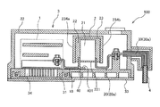
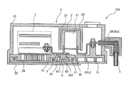
- FIG. 1 is a schematic cross-sectional view of the power conversion device according to the first embodiment.
- FIG. 2 is a schematic cross-sectional view of the power conversion device according to the first embodiment at a position different from that of FIG.
- FIG. 3 is a bottom perspective view of the smoothing capacitor.
- FIG. 4 is a cross-sectional view of the base portion of the housing before the cover portion is attached.
- FIG. 5 is an attachment diagram of the smoothing capacitor.
- FIG. 6 is a schematic cross-sectional view of the power conversion device according to the modification of the first embodiment.
- FIG. 7 is a schematic cross-sectional view of the power conversion device according to the second embodiment.
- FIG. 8 is a bottom perspective view of the smoothing capacitor.
- FIG. 9 is a schematic sectional view of a power conversion device according to a modified example of the second embodiment.
- FIG. 10 is a schematic sectional view of the power conversion device according to the third embodiment.
- FIG. 11 is a schematic sectional view of the power conversion device according to the fourth embodiment.
- FIG. 12 is a schematic sectional view of a power conversion device according to a modification of the fourth embodiment.
- FIG. 13 is a bottom perspective view of the smoothing capacitor.
- FIG. 14 is a schematic sectional view of the power conversion device according to the fifth embodiment.
- FIG. 15 is a bottom perspective view of the smoothing capacitor.
- FIG. 16 is a schematic sectional view of the power conversion device according to the sixth embodiment.
- FIG. 17 is a schematic cross-sectional view of the power converter showing the appearance of the smoothing capacitor.
- FIG. 18 is a cross-sectional schematic diagram of the power converter device of other embodiment.
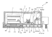
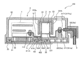
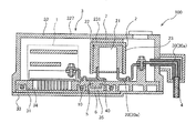
- FIG. 1 and 2 are schematic cross-sectional views of the power converter according to the first embodiment.
- FIG. 1 is a cross-sectional view of a portion including a conductor portion for input
- FIG. 2 is a cross-section of a portion including a conductor portion for output. It is a figure.
- the power conversion device 100 includes an inverter 1, a smoothing capacitor 2, and a housing 3, and is mounted on a vehicle or the like.
- the inverter 1 and the smoothing capacitor 2 are housed in the housing 3. Further, the inverter 1 and the smoothing capacitor 2 are electrically connected by a plurality of conductor portions 10 (first conductor portion), and the smoothing capacitor 2 and the power source 4 outside the housing are provided with a plurality of conductor portions 20, 30 (second conductor portion). It is electrically connected by a conductor part).
- the inverter 1 is composed of a plurality of electric components, includes a power module 11 having a built-in semiconductor element and a control board 12 having a control circuit, and has a function of converting electric power into direct current or alternating current.
- the power module 11 is configured by combining a plurality of semiconductor elements.
- the power module 11 is placed on the substrate 111 and fixed on the substrate 111 with bolts or the like.
- the substrate 111 is fixed to the base portion 31 of the housing 3 described later with bolts or the like.
- the power module 11 is electrically connected to the control board 12 and is also connected to the smoothing capacitor 2 via the conductor portion 10.
- the conductor portion 10 is fixed to the power module 11 with a bolt or the like at a terminal portion 112 provided on the power module 11.
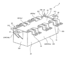
- the smoothing capacitor 2 includes a capacitor element 21, a filling material 22, and a capacitor case 23, and is arranged side by side with the inverter 1 in a substantially horizontal direction.
- the capacitor case 23 is made of a resin such as polyphenylene sulfide (PPS) or polyphthalamide (PPA), and accommodates the capacitor element 21.
- the capacitor element 21 is connected to the power module 11 of the inverter 1 via the conductor portion 10 and also connected to the power source 4 outside the housing 3 via the conductor portions 20 and 30.
- the filling material 22 is, for example, a potting material containing silicone, fills the periphery of the capacitor element 21, and fixes the capacitor element 21 in the capacitor case 23.
- the housing 3 is provided on the lower surface of the base portion 31, the base portion 31 on which the inverter 1 and the smoothing capacitor 2 are placed, the cover portion 32 attached to the base portion 31 so as to cover the inverter 1 and the smoothing capacitor 2, It is composed of a thin plate 33 that functions as a bottom plate of the cover portion 32.
- the base portion 31 is configured as a plate-shaped member of an electrically insulating resin material such as polyphenylene sulfide (PPS) or polyphthalamide (PPA), and the inverter 1 and the smoothing capacitor 2 are mounted on the mounting surface 311.
- the base portion 31 includes a cooling path 34 (first refrigerant flow path) below a portion where the inverter 1 is mounted, through which cooling water (refrigerant) that cools the inverter 1 flows.
- a metal thin plate 33 made of aluminum or the like, which is larger than the outer shape of the lower surface 312, is provided.
- a substrate 111 having an outer shape larger than that of the cooling passage 34 is installed on the upper surface of the cooling passage 34 of the base portion 31, and the substrate 111 is fastened to the base portion 31 with a bolt or the like.
- a fin 113 is provided below the power module 11.
- the substrate 111 is provided with a plurality of holes through which the fins 113 pass, and the fins 113 are in contact with the cooling water in the cooling passage 34 through the holes.
- the power module 11 is provided with the fins 113 and brought into contact with the cooling water, the invention is not necessarily limited thereto and the fins 113 may not be provided.
- the cover part 32 is formed of a metal material such as aluminum, and is attached to the base part 31 so as to cover the periphery of the inverter 1 and the smoothing capacitor 2.
- the cover part 32 is composed of an upper wall 321 and a side wall 322.
- the side wall 322 has an opening 323 a (FIG. 1) opened so that the input conductor part 30 a connected to the power supply 4 passes through and the power supply 4 is provided.
- An opening 323b (FIG. 2) is formed so as to pass through the connecting output conductor 30b.
- a step portion 324 having an end surface that abuts on the mounting surface 311 of the base portion 31 is formed inside the side wall 322.
- the tip surface 325 of the side wall 322 abuts the outer peripheral edge 331 of the thin plate 33 provided on the lower surface 312 of the base portion 31.
- the cover portion 32, the base portion 31, and the thin plate 33 are fastened together by bolts or the like from the outside of the thin plate 33 at the portion where the step portion 324 of the cover portion 32 and the mounting surface 311 of the base portion 31 contact each other. It In this way, by completely covering the inverter 1 and the smoothing capacitor 2 with the cover portion 32 and the thin plate 33 formed of the metal material, it is possible to enhance the electromagnetic shielding property of the power conversion device 100.
- An openable/closable lid portion 326 may be provided on the upper wall 321 of the cover portion 32 so that the fastening of the conductor portion 20 and the conductor portion 30 described below can be maintained.
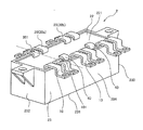
- FIG. 3 is a bottom perspective view of the smoothing capacitor 2.
- the capacitor case 23 of the smoothing capacitor 2 accommodates the capacitor element 21 inside, and the periphery of the capacitor element 21 is filled with the filling material 22.
- the periphery of the filler 22 is covered with the upper surface 231, the front surface 232, the rear surface 233, and the side surface 234 of the capacitor case 23.
- the bottom surface of the capacitor case 23 is open, and the filling material 22 forms a potting surface 221 on the bottom surface of the smoothing capacitor 2.
- the capacitor case 23 includes a bracket 24 protruding outward from the front surface 232 and the rear surface 233 and a positioning pin 25 protruding downward from the bottom surface.
- the bracket 24 is a member for fastening the smoothing capacitor 2 to the housing 3.
- the bracket 24 is provided with a hole portion 241 through which a bolt or the like for fastening the smoothing capacitor 2 to the base portion 31 passes.
- the positioning pin 25 is a member that determines the horizontal position of the smoothing capacitor 2 in the housing 3.
- the positioning pin 25 connects a corner portion 235 where the one side surface 234b of the capacitor case 23 on the bottom surface of the smoothing capacitor 2 connects to the front surface 232, and one side surface 234b of the capacitor case 23 on the bottom surface of the smoothing capacitor 2 connects to the rear surface 233.
- Each of the corners 236 projects downward from the bottom surface.
- the positioning pin 25 is provided at each of the corners 235 and 236 where the one side surface 234b of the capacitor case 23 on the bottom surface of the smoothing capacitor 2 is connected to the front surface 232 and the rear surface 233.
- the number and position are not limited to this. For example, it may be provided at all four corners on the bottom surface of the smoothing capacitor 2.
- a plurality of conductors 10 and 20 connected to the capacitor element 21 extend from the potting surface 221 to the outside of the smoothing capacitor 2.
- the conductor portion 10, the conductor portion 20 and the conductor portion 30 described later are metal bus bars made of, for example, copper or aluminum having good conductivity.
- the conductor portion 10 projects to the outside of the smoothing capacitor 2 from the vicinity of the one side surface 234a of the capacitor case 23 in the potting surface 221, and electrically connects the capacitor element 21 and the power module 11 of the inverter 1. Further, the conductor portion 20 projects outside the smoothing capacitor 2 from the vicinity of the other side surface 234b of the capacitor case 23 on the potting surface 221, and connects the capacitor element 21 and the power source 4 outside the power conversion device 100 via the conductor portion 30.
- the conductor portion 20 and the conductor portion 30 respectively include an input conductor portion 20a and a conductor portion 30a for inputting electric power from the power source 4, and an output conductor portion 20b and a conductor portion 30b for outputting electric power to the power source 4. ..
- the details of the arrangement of the conductors will be described later.
- FIG. 4 is a cross-sectional view of the base portion 31 of the housing 3, showing the base portion 31 before the cover portion 32 is attached.
- FIG. 5 is a cross-sectional view of the power conversion device 100, and is a mounting view of the smoothing capacitor 2.
- the base portion 31 is formed of an electrically insulating resin material, and is composed of a main body portion 313 and a bottom plate portion 314 as shown in FIG.
- the main body 313 has an opening 315 for forming the cooling passage 34, a joint 316 for joining the bottom plate 314, and a terminal 317 for fastening the conductor 20 and the conductor 30.
- the main body portion 313 further includes a holding portion 318 for holding the smoothing capacitor 2 and a pin receiving portion 319 through which the positioning pin 25 for positioning the smoothing capacitor 2 is inserted.
- the opening 315 of the main body 313 is provided in the base 31 where the inverter 1 is mounted, and the top and bottom are open.
- the joint portion 316 is a portion into which a convex portion 3141 of the bottom plate portion 314 described later is inserted and joined.
- the joint portion 316 is a hole whose lower surface is opened, and is provided around the opening portion 315.
- the bottom plate 314 has a larger outer shape than the opening 315 of the main body 313, and has a convex portion 3141 projecting upward from the upper surface of the bottom plate 314 at a position corresponding to the joint 316 of the main body 313.
- the convex portion 3141 and the joint portion 316 of the main body portion 313 are joined together by welding or the like, and the main body portion 313 and the bottom plate portion 314 are joined together to form a concave portion 341 at the position of the opening 315.
- the recess 341 is a groove for forming the cooling path 34 through which the cooling water for cooling the inverter 1 flows. As shown in FIG. 5, by covering the upper portion of the recess 341 with the substrate 111 of the power module 11, the cooling passage 34 (first refrigerant passage) surrounded by the main body portion 313, the bottom plate portion 314, and the substrate 111 is formed. It
- the terminal portion 317 of the main body portion 313 is a portion to which the conductor portion 20 connected to the smoothing capacitor 2 and the conductor portion 30 connected to the power source 4 are connected, and the smoothing capacitor 2 is installed. It is provided at a position between the location where the side wall 322 and the side wall 322 of the housing 3.
- the terminal portion 317 is integrally provided with the base portion 31 so as to project upward from the mounting surface 311 of the base portion 31, and the conductor portion 20 and the conductor portion 30 are provided on the upper surface 3171 of the terminal portion 317. It is fastened by being fastened to the base part together with bolts and the like. In this way, by providing the terminal portion 317 integrally with the base portion 31 forming the housing 3, it is possible to reduce the cost as compared with the case where the terminal portion 317 is provided as a separate member.
- the holding portion 318 of the main body portion 313 is a portion for holding the smoothing capacitor 2, and is configured to project upward from the mounting surface 311 of the base portion 31 at a position where the bracket 24 of the smoothing capacitor 2 faces. It is provided.
- the smoothing capacitor 2 is fastened to the holding portion 318 with a bolt or the like through the hole 241 of the bracket 24. Accordingly, the vertical movement of the smoothing capacitor 2 with respect to the housing 3 is restricted.
- the pin receiving portion 319 of the main body portion 313 is provided at a position corresponding to the positioning pin 25 of the smoothing capacitor 2 so as to project upward from the mounting surface 311 of the base portion 31. By inserting the positioning pin 25 into the pin receiving portion 319, the horizontal position of the smoothing capacitor 2 with respect to the housing 3 is positioned.
- the capacitor case 23 is provided with the positioning pin 25 and the base portion 31 is provided with the pin receiving portion 319 as described above, but these are not necessarily provided. ..
- a cavity 3101 having an open bottom may be formed in a portion of the base 31 where the cooling passage 34 is not provided. This reduces the weight of the power conversion device 100.
- the number and shape of the hollow portions 3101 are not particularly limited, and for example, one large hollow portion may be provided, or the bottom surface may be closed.
- the conductor portion 10 that electrically connects the inverter 1 and the smoothing capacitor 2 has one end connected to the capacitor element 21 of the smoothing capacitor 2 and downward from the potting surface 221 of the smoothing capacitor 2. Project toward.
- the other end of the conductor portion 10 is fixed to the power module 11 with a bolt or the like at a terminal portion 112 provided on the power module 11 of the inverter 1.
- the inverter 1 and the smoothing capacitor 2 are electrically connected by the conductor portion 10.
- the conductor portion 10 is close to the base portion 31 of the housing 3 while the capacitor element 21 of the smoothing capacitor 2 and the power module 11 of the inverter 1 are being connected. As described above, even if the conductor portion 10 is arranged at a position close to the base portion 31, since the base portion 31 is formed of an insulating material, the insulation between the conductor portion 10 and the housing 3 is not increased. Secured. Further, since the conductor portion 10 is close to the base portion 31, the heat of the conductor portion 10 is also dissipated by the base portion 31 via the space between the base portion 31 and the conductor portion 10. Here, since the base portion 31 includes the cooling passage 34, the base portion 31 is also cooled by the cooling water flowing through the cooling passage 34. Therefore, heat is exchanged between the base portion 31 and the conductor portion 10 cooled by the cooling water, and the smoothing capacitor 2 connected to the conductor portion 10 is cooled.
- the conductor portion 20 and the conductor portion 30 are members that electrically connect the smoothing capacitor 2 and the power source 4 outside the housing 3.
- the conductor portion 20 includes an input conductor portion 20a and an output conductor portion 20b
- the conductor portion 30 includes an input conductor portion 30a and an output conductor portion 30b.
- one end of each of the conductor portions 20 a and 20 b is connected to the capacitor element 21 of the smoothing capacitor 2 and projects downward from the potting surface 221 of the smoothing capacitor 2.
- the other ends of the conductor portions 20a and 20b are connected to the conductor portions 30a and 30b at the upper surfaces 3171a and 3171b of the terminal portions 317a and 317b protruding upward from the mounting surface 311 of the base portion 31.
- the conductor portions 20a, 20b and the conductor portions 30a, 30b are fastened together with the base portion 31 by bolts or the like on the upper surfaces 3171a, 3171b of the terminal portions 317a, 317b.
- the conductor portions 20a and 20b are close to the base portion 31 of the housing 3 while the capacitor element 21 of the smoothing capacitor 2 and the conductor portions 30a and 30b are being connected.
- the base portion 31 is formed of an insulating material
- the space between the conductor portions 20a and 20b and the housing 3 is reduced.
- the insulating property of is secured.
- the heat of the conductor portions 20a and 20b passes through the space between the base portion 31 and the conductor portions 20a and 20b. Heat is also removed to 31. That is, similar to the conductor portion 10, heat is exchanged between the base portion 31 and the conductor portions 20a and 20b cooled by the cooling water, and the smoothing capacitor 2 to which the conductor portions 20a and 20b are connected is cooled.
- each of the conductor portions 30a and 30b is connected to the conductor portions 20a and 20b on the upper surfaces 3171a and 3171b of the terminal portions 317a and 317b, and the casing portions 3a to 323b are opened through the opening portions 323a and 323b. Be extended outside.
- the other ends of the conductor portions 30a and 30b are connected to the external power source 4. In this way, the smoothing capacitor 2 and the power supply 4 are electrically connected to each other through the input conductor portion 20a and the conductor portion 30a and the output conductor portions 20b and 30b.
- the length of the portion where the conductor portion 10 and the conductor portion 20 are close to the base portion 31 is not particularly limited, but in order to further increase the cooling effect of the cooling water, it is preferable that the distance between the adjacent portions is as long as possible.
- the six conductor portions 10, two conductor portions 20a and two conductor portions 20b respectively project from the smoothing capacitor 2, but the number of conductor portions is not limited to this.
- the housing 3 is made of a resin material, and the base portion 31 on which the inverter 1 and the smoothing capacitor 2 are mounted and the cover portion 32 attached to the base portion 31 so as to cover the inverter 1 and the smoothing capacitor 2 are included. And consists of.
- the conductor portion 10 (first conductor portion) that connects the smoothing capacitor 2 and the inverter 1 is close to the base portion 31 of the housing 3 while the smoothing capacitor 2 and the inverter 1 are being connected. In this way, by forming the base portion 31 with an insulating material, the insulation between the conductor portion 10 and the housing 3 is ensured, and the conductor portion 10 is arranged at a position close to the base portion 31. ..
- the power conversion device 100 includes conductor portions 20 and 30 (second conductor portions) that connect the smoothing capacitor 2 and the power source 4 outside the housing 3, and the conductor portion 20 includes the smoothing capacitor 2 and the power source 4.
- the base portion 31 is formed of an insulating material, it is not necessary to interpose another member such as an insulating material between the conductor portion 20 and the housing 3 as in the conductor portion 10, and the cost is reduced. Is possible.
- the conductor portion 20 is arranged at a position close to the base portion 31, space can be saved as compared with the case where the insulating space distance between the conductor portion 20 and the housing 3 is increased. That is, it is possible to provide a power conversion device that is low in cost and space-saving while ensuring insulation between the conductor portion 20 connected to the smoothing capacitor 2 and the housing 3.
- the base portion 31 of the power conversion device 100 includes a cooling passage 34 (first refrigerant passage) through which cooling water (refrigerant) for cooling the inverter 1 flows.
- a cooling passage 34 first refrigerant passage
- the inverter 1 is directly cooled, and the base portion 31 is also cooled by heat exchange between the cooling water and the base portion 31.
- the conductor portions 10 and 20 are close to the base portion 31, the heat of the conductor portions 10 and 20 is also removed by the base portion 31 via the space between the base portion 31 and the conductor portions 10 and 20. Therefore, heat is exchanged between the base portion 31 and the conductor portions 10 and 20 cooled by the cooling water, and the cooling performance of the smoothing capacitor 2 to which the conductor portions 10 and 20 are connected can be improved. That is, it is possible to provide a power conversion device that improves the cooling effect of the smoothing capacitor 2 while ensuring insulation between the conductors 10 and 20 connected to the smoothing capacitor 2 and the housing 3.
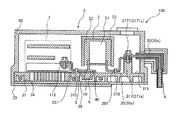
- FIG. 6 is a schematic cross-sectional view of a power conversion device 100 according to a modified example of the first embodiment.
- the conductor portion 10 is arranged so as to come into contact with the base portion 31 of the housing 3 while the capacitor element 21 of the smoothing capacitor 2 and the power module 11 of the inverter 1 are being connected. To be done. As described above, even if the conductor portion 10 is brought into contact with the base portion 31, since the base portion 31 is formed of the insulating material, the insulating property between the conductor portion 10 and the housing 3 is ensured.
- the base portion 31 of the housing 3 is formed of an insulating resin material, and the conductor portion 10 (first conductor portion) that connects the smoothing capacitor 2 and the inverter 1 is the smoothing capacitor 2 and the inverter 1.
- the base portion 31 of the housing 3 is contacted during the connection between and. That is, the base portion 31 is formed of an insulating material to ensure insulation between the conductor portion 10 and the housing 3, and the conductor portion 10 is arranged so as to contact the base portion 31. Since the space between the conductor portion 10 and the housing 3 is eliminated by bringing the conductor portion 10 into contact with the housing 3 in this manner, it is possible to further save the space of the power conversion device. That is, it is possible to provide a space-saving power conversion device while ensuring insulation between the conductor portion 10 connected to the smoothing capacitor 2 and the housing 3.
- the conductor portion 10 since the conductor portion 10 is in contact with the base portion 31 of the housing 3, heat exchange is performed between the cooling water flowing through the cooling passage 34 (first refrigerant passage) and the conductor portion 10 via the base portion 31. Is done. That is, heat is exchanged between the cooling water and the conductor portion 10 without passing through the space between the conductor portion 10 and the base portion 31. Therefore, compared with the case where the conductor portion 10 is not in contact with the base portion 31 of the housing 3, the cooling effect of the cooling water flowing through the cooling passage 34 is more easily transmitted to the conductor portion 10, and the smoothing capacitor connected to the conductor portion 10 is more easily transmitted.
- the cooling performance of No. 2 can be further improved. That is, it is possible to provide a power conversion device that further improves the cooling performance of the smoothing capacitor 2 while ensuring the insulation between the housing 3 and the conductor portion 10.
- both the conductor portion 10 and the conductor portion 20 may be arranged to be in contact with the base portion 31, or only the conductor portion 20 may be arranged.
- the conductor portion 10 may be arranged so as to be in contact with the base portion 31 and be close to the base portion 31.
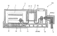
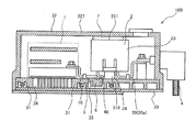
- FIG. 7 is a schematic cross-sectional view of the power conversion device 100 according to the second embodiment
- FIG. 8 is a bottom perspective view of the smoothing capacitor 2.
- the present embodiment is different from the first embodiment and the modification of the first embodiment in that a conductor portion 40 (third conductor portion) dedicated to cooling is provided.
- the smoothing capacitor 2 has a potting surface 221 formed by the filler 22 on the bottom surface. From the potting surface 221, in addition to the conductor portion 10 and the conductor portion 20, the conductor portion 40 is outside the capacitor. Be extended to.
- the conductor section 40 is a member for cooling the capacitor, and is made of, for example, copper or aluminum having good conductivity. As shown in FIG. 7, the conductor portion 40 has one end connected to the capacitor element 21 and the other end in contact with the base portion 31. Further, the conductor portion 40 projects from the vicinity of the one side surface 234 a of the capacitor case 23 on the potting surface 221 to the outside of the smoothing capacitor 2 and extends to a position where it contacts the base portion 31. The conductor portion 40 is bent at a position in contact with the base portion 31, and is extended inward of the smoothing capacitor 2 while being in contact with the base portion 31. Thereby, the contact surface 401 where the conductor portion 40 and the base portion 31 contact each other is formed.
- the conductor portion 40 contacts the base portion 31, heat is exchanged between the cooling water flowing through the cooling passage 34 and the conductor portion 40 through the base portion 31, and the conductor portion 40 and the conductor portion 40 are exchanged.
- the smoothing capacitor 2 connected to is cooled. That is, by providing the conductor portion 40 dedicated to cooling, the cooling effect of the cooling water is transmitted to the conductor portion 40 via the base portion 31, so that the cooling performance of the smoothing capacitor 2 is further improved. Further, even if the conductor portion 40 is arranged at a position in contact with the base portion 31 as described above, since the base portion 31 is made of an insulating material, the insulating property between the conductor portion 40 and the housing 3 is reduced. Is secured.
- the conductor portion 40 is bent at a position where it comes into contact with the base portion 31, and a contact surface 401 is formed between the conductor portion 40 and the base portion 31, so that the conductor portion 40 and the base portion 31 are separated from each other.
- the contact area is expanded, and the cooling performance of the smoothing capacitor 2 is further improved.
- the power conversion device 100 includes a base portion 31 of the housing 3 formed of an insulating resin material and a conductor portion 40 for cooling the smoothing capacitor 2.
- the conductor portion 40 has a portion that is connected to the smoothing capacitor 2 and that contacts the base portion 31 of the housing 3. That is, the base portion 31 is made of an insulating material to ensure insulation between the conductor portion 40 and the housing 3, and the conductor portion 40 is in contact with the base portion 31.
- heat is exchanged between the cooling water flowing through the cooling passage 34 and the conductor portion 40 via the base portion 31.
- the cooling effect of the cooling water flowing through the cooling passage 34 is transmitted to the conductor portion 40 via the base portion 31, so that the cooling performance of the smoothing capacitor 2 connected to the conductor portion 40 is further improved. Therefore, it is possible to provide a power conversion device in which the cooling effect of the smoothing capacitor 2 is further improved while ensuring the insulation between the housing 3 and the conductor portion 40.
- the conductor portion 40 be disposed in contact with the base portion 31 as in the present embodiment, but the present invention is not limited to this, and the conductor portion 40 is not limited thereto. It may be arranged at a position close to 31.
- the conductor portion 40 is bent inward of the smoothing capacitor 2, but the bending direction may be outward of the smoothing capacitor 2.
- the conductor portion 40 is provided so as to project from the vicinity of the one side surface 234a of the capacitor case 23 to the outside of the smoothing capacitor 2, but the conductor portion 40 is provided on the other side surface 234b of the capacitor case 23. You may provide so that it may protrude from the vicinity.
- the positioning pin 25 is not provided in the capacitor case 23, but the positioning pin 25 and the pin receiving portion 319 may be provided to position the smoothing capacitor 2 as in the first embodiment.
- a power converter 100 according to a modification of the second embodiment will be described with reference to FIG. 9.
- the same elements as those of the other embodiments are designated by the same reference numerals, and the description thereof will be omitted.
- FIG. 9 is a schematic cross-sectional view of a power conversion device 100 according to a modified example of the second embodiment. As shown in FIG. 9, in this modification, the conductor portion 10 (first conductor portion) and the conductor portion 40 (third conductor portion) are not in direct contact with the base portion 31, and the conductor portion 10 and the conductor portion 10 are not directly in contact with each other.
- the elastic conductive member 5 is sandwiched between 40 and the base portion 31 of the housing 3.
- the conductor portion 10 protruding from the potting surface 221 formed on the bottom surface of the smoothing capacitor 2 is close to the base portion 31 of the housing 3 while the smoothing capacitor 2 and the inverter 1 are being connected. ..
- the conductor portion 40 protruding from the potting surface 221 formed on the bottom surface of the smoothing capacitor 2 is bent inward of the smoothing capacitor 2 at a position close to the base portion 31 of the housing 3. Note that the bending direction may be the outside direction of the smoothing capacitor 2 as in the second embodiment.
- the elastic conductive member 5 is interposed between the conductor portions 10 and 40 and the base portion 31.
- the elastic conductive member 5 is, for example, highly conductive grease, an adhesive, a sheet, or the like, and is provided between the conductor portions and the base portion 31 at the portions where the conductor portions 10 and 40 and the base portion 31 are close to each other.
- the upper surface 51 of the elastic conductive member 5 contacts the conductor portions 10 and 40, and the bottom surface 52 contacts the base portion 31.
- the elastic conductive member 5 is dimensioned between the conductor portions 10 and 40 and the base portion 31. Fulfills the tolerance absorbing function.
- the heat transfer coefficient between the conductor portions 10 and 40 and the base portion 31 can be improved as compared with the case where the conductor portions 10 and 40 are brought into direct contact with the base portion 31. That is, the heat exchange rate between the cooling water flowing through the cooling passage 34 and the conductor portions 10, 40, which is performed via the base portion 31, is improved.
- the base portion 31 is formed of an insulating material. Insulation between the conductor portions 10 and 40 and the housing 3 is ensured.
- the power conversion device 100 includes a base portion 31 of the housing 3 formed of an insulating resin material, an elastic conductive member 5 that contacts the base portion 31, and a conductor portion 10 (first conductor portion) and a conductor portion 40.
- the (third conductor portion) comes into contact with the elastic conductive member 5 in the portion close to the base portion 31. That is, by forming the base portion 31 with an insulating material, the insulation between the conductor portions 10 and 40 and the housing 3 is ensured, and the conductor portions 10 and 40 are connected via the elastic conductive member 5 to the base portion 31. Is in contact with.
- the elastic conductive member 5 is The dimensional tolerance between 40 and the base portion 31 is absorbed.
- the thermal conductivity between the conductor portions 10 and 40 and the base portion 31 can be improved as compared with the case where the conductor portions 10 and 40 are brought into direct contact with the base portion 31. Therefore, the heat exchange rate between the cooling water flowing through the cooling passage 34 and the conductor portions 10 and 40 performed via the base portion 31 is improved, and the cooling performance of the smoothing capacitor 2 can be further improved. That is, it is possible to provide a power conversion device that further improves the cooling performance of the smoothing capacitor 2 while ensuring the insulation between the housing 3 and the conductor portions 10 and 40.
- the elastic conductive member 5 is interposed between the conductor portions 10 and 40 and the base portion 31 in the present embodiment, the conductor portion 20 and the base portion are provided in a portion where the conductor portion 20 and the base portion 31 are close to each other. An elastic conductive member 5 that contacts the portion 31 may be provided.
- the power converter 100 according to the third embodiment will be described with reference to FIG. 10.
- the same elements as those of the other embodiments are designated by the same reference numerals, and the description thereof will be omitted.
- FIG. 10 is a schematic cross-sectional view of the power conversion device 100 according to the third embodiment.
- the base portion 31 includes a second cooling passage 35 (second refrigerant passage) below the elastic conductive member 5 through which cooling water (refrigerant) flows.
- the main body portion 313 of the base portion 31 has a recess 351 whose bottom surface is open below the position where the conductor portions 10 and 40 face each other, that is, below the elastic conductive member 5. Further, the main body portion 313 has a joint portion 316 which is a hole whose lower surface is opened around the opening 315 and around the recess 351.
- the bottom plate portion 314 of the base portion 31 has an outer shape that is large enough to cover the bottom surfaces of both the opening 315 and the recessed portion 351 of the main body portion 313, and is located at a position corresponding to the joint portion 316.
- the convex portion 3141 and the joint portion 316 of the main body portion 313 are joined by welding or the like, and the main body portion 313 and the bottom plate portion 314 are joined, so that the main body portion 313, the bottom plate portion 314, and the power module are located at the positions of the openings 315.
- the cooling path 34 surrounded by the substrate 111 of 11 is formed.
- a second cooling passage 35 surrounded by the main body portion 313 and the bottom plate portion 314 is formed at the position of the concave portion 351.
- the cooling passage 35 is a passage through which cooling water for cooling the smoothing capacitor 2 flows, and is formed below the position where the conductor portions 10 and 40 face each other, that is, below the elastic conductive member 5, and the cooling passage 35 is formed. Connect to 34. Therefore, the cooling water circulates through the cooling passage 34 and the cooling passage 35 and flows. As described above, by providing the second cooling passage 35 below the position where the conductor portions 10 and 40 face each other, the conductor portions 10 and 40 and the cooling water can be separated from each other as compared with the case where the base portion 31 has only the cooling passage 34. The heat transfer path between them is shortened, and the cooling performance of the smoothing capacitor 2 can be further improved.
- the conductor portions 10 and 40 are in contact with the base portion 31 of the housing 3 via the elastic conductive member 5 having high conductivity, but the base portion 31 has an insulating property. Since it is formed of the above material, the insulation between the conductor portions 10 and 40 and the housing 3 is secured.
- cooling passage 34 and the cooling passage 35 are located upstream of the cooling passage 34 when it is desired to cool the inverter 1 (power module 11) more than at the smoothing capacitor 2, and when the cooling of the smoothing condenser 2 is desired. Should be on the upstream side.
- the base portion 31 of the housing 3 is formed of an insulating resin material, and the base portion 31 is below the portion facing the conductor portions 10 and 40, that is, below the elastic conductive member 5.
- a cooling passage 35 (second refrigerant passage) through which cooling water (refrigerant) flows is provided. That is, by forming the base portion 31 with an insulating material, the insulation between the conductor portions 10 and 40 and the housing 3 is secured, and below the elastic conductive member 5 with which the conductor portions 10 and 40 contact.
- a second cooling passage 35 is provided.
- the heat transfer path between the conductor portions 10 and 40 and the cooling water is shortened, and the cooling performance of the smoothing capacitor 2 is reduced as compared with the case where the base portion 31 has only the cooling passage 34 for cooling the inverter 1. Further improve. That is, it is possible to further improve the cooling performance of the smoothing capacitor 2 while ensuring the insulation between the housing 3 and the conductor portions 10 and 40.
- the elastic conductive member 5 is interposed between the conductor portions 10 and 40 and the base portion 31 in the present embodiment, the conductor portions 10 and 40 are directly connected to the base portion 31 without the elastic conductive member 5. May be contacted with.
- the cooling passage 34 and the cooling passage 35 are connected to each other, and the cooling water is circulated between the cooling passage 34 and the cooling passage 35.
- the cooling passage 34 and the cooling passage 35 are respectively provided. It is also possible to use a separate independent flow path, in which both flow paths are not connected.
- the cooling passage 35 is provided in the portion of the base portion 31 facing the conductor portions 10 and 40, but the cooling passage 35 is provided only in the position facing either the conductor portion 10 or the conductor portion 40. May be provided, or the cooling path 35 may be provided in a portion facing the conductor portion 20. Further, the cooling passage 45 may be provided in a portion of the base portion 31 facing the conductor portions 10 and 40, and another cooling passage may be provided in a portion of the base portion 31 facing the conductor portion 20.
- FIG. 11 is a schematic sectional view of the power conversion device 100 according to the fourth embodiment. As shown in FIG. 11, the present embodiment differs from the third embodiment in that the base portion 31 includes the metal member 6.
- the base portion 31 includes a cooling passage 35 (second refrigerant passage) through which cooling water for cooling the smoothing condenser 2 flows, and a metal member 6 provided at a position facing the cooling passage 35.
- the cooling path 35 has a substantially U-shaped cross-sectional shape in which a recess 352 is formed at the center of the cross section as viewed from the front.
- the metal member 6 is made of a metal material having a high thermal conductivity, such as copper or aluminum, and is provided at a position facing the cooling passage 35 directly below the elastic conductive member 5.
- the metal member 6 has a T-shape in a cross section when viewed from the front of the cooling passage 35, and projects toward the upper portion 61 having the upper surface 611 that contacts the elastic conductive member 5 and the recess 351 of the cooling passage 35. It is composed of the convex portion 62.
- the metal member 6 is integrally provided on the base portion 31 by insert molding, outsert molding by press fitting, or the like.
- the metal member 6 having high thermal conductivity is provided at a position facing the cooling path 35 so as to project toward the cooling path 35, the heat of the conductor portions 10 and 40 connected to the smoothing capacitor 2 is reduced. Can be efficiently transferred to the vicinity of the cooling path 35 via the elastic conductive member 5 and the metal member 6. Further, since the base portion 31 made of a resin material is interposed between the metal member 6 and the cooling passage 35, insulation between the metal member 6 and the housing 3 and the cooling water is ensured. Insulation between the conductor portions 10 and 40 and the housing 3 is ensured.
- the cooling passage 35 is provided in a substantially U-shaped shape in a cross section viewed from the front direction, the contact surface area between the cooling water and the base portion 31 is larger than that in the case where the round or square cooling passage is provided. Will grow. Thereby, the heat exchange rate between the cooling water and the base portion 31 is improved, and the heat exchange rate between the cooling water and the conductor portions 10 and 40 performed via the base portion 31 is also improved. Therefore, the cooling performance of the smoothing capacitor 2 connected to the conductor portions 10 and 40 is further improved.
- the base portion 31 of the housing 3 is formed of an insulating resin material
- the base portion 31 includes a metal member 6 that contacts the elastic conductive member 5, and the metal member 6 faces the cooling path 35. It is provided at the position where In this way, since the metal member 6 that contacts the elastic conductive member 5 is provided at the position facing the cooling path 35, the heat of the conductor portions 10 and 40 connected to the smoothing capacitor 2 is applied to the elastic conductive member 5 and the metal member 6. The heat can be efficiently transferred to the vicinity of the cooling path 35 via.
- the base portion 31 made of a resin material is interposed between the metal member 6 and the cooling passage 35, insulation between the metal member 6 and the housing 3 and the cooling water is ensured. Insulation between the conductor portions 10 and 40 and the housing 3 is ensured. Therefore, the cooling efficiency of the smoothing capacitor 2 can be further improved while ensuring the insulation between the conductors 10 and 40 and the housing 3.
- the metal member 6 contacting the elastic conductive member 5 also functions as a heat mass for accumulating the heat of the conductor portions 10 and 40. Therefore, since the heat capacity of the base portion 31 is increased by the metal member 6, the temperature rise of the smoothing capacitor 2 connected to the conductor portions 10 and 40 can be suppressed to a low level, and the transient thermal performance of the smoothing capacitor 2 is improved.
- the metal member 6 is provided directly below the elastic conductive member 5 that contacts the conductor portions 10 and 40. However, below the conductor portion 20, the elastic conductive member 5 and the metal that contacts the elastic conductive member 5 are provided. The member 6 and the cooling passage 35 may be provided.
- the cross section of the cooling passage 35 is formed in a substantially U shape, and the cross section of the metal member 6 is formed in a T shape in order to bring the metal member 6 closer to the cooling water.
- the shapes of the cooling passage 35 and the metal member 6 are not necessarily limited to this. If the metal member 6 contacts the elastic conductive member 5 and the base portion 31 is interposed between the metal member 6 and the cooling passage 35, the cooling passage 35 and the metal member 6 may have any shape.
- FIG. 12 is a schematic sectional view of a power conversion device 100 according to a modified example of the fourth embodiment
- FIG. 13 is a bottom perspective view of the smoothing capacitor 2.
- the base portion 31 has a protrusion 310 for positioning the smoothing capacitor 2
- the conductors 10 and 20 have holes 101, through which the protrusion 310 is inserted.
- 201 positioning hole
- the base portion 31 has a surface (mounting surface 311) on which the inverter 1 and the smoothing capacitor 2 are mounted, at positions corresponding to holes 101 and 201 of conductor portions 10 and 20 described later. It has a protruding portion 310 that protrudes.
- the protruding portion 310 is provided integrally with the base portion 31 and is inserted into the holes 101 and 201 of the conductor portions 10 and 20.
- the projecting portions 310 of the base portion 31 are inserted in locations close to the base portion 31, respectively.
- the holes 101 and 201 are provided.
- the holes 101 and 201 are provided in the conductor portion 10 and the conductor portion 20 that are arranged to face each other among the plurality of conductor portions 10 and 20, and the center point of the hole 101 of the conductor portion 10 and the conductor portion 10 face each other.
- the center point of the hole 201 of the conductor portion 20 is arranged on a straight line parallel to the front surface 232 and the rear surface 233 of the smoothing capacitor 2.
- the holes 101 and 201 are preferably provided in the conductor portion 10 and the conductor portion 20 arranged to face each other, from the viewpoint of ensuring the positioning stability of the smoothing capacitor 2, but not limited to this.
- they may be provided in the conductor portions that do not face each other, or a positioning hole may be provided in the conductor portion 40.
- the holes 101 and 201 are provided in the conductor portion 10 and the conductor portion 20, respectively, but the number of conductor portions in which the holes 101 and 201 are provided is not limited to this. You may provide a positioning hole in.
- the power conversion device 100 has a projecting portion 310 in which the base portion 31 of the housing 3 projects from the surface (mounting surface 311) on which the inverter 1 and the smoothing capacitor 2 are mounted, and projects into the conductor portions 10 and 20. Holes (positioning holes) 101 and 201 into which the portion 310 is inserted are provided. By inserting the protruding portion 310 of the base portion 31 into the holes 101 and 201 of the conductor portions 10 and 20, the smoothing capacitor 2 is positioned and the conductor portions 10 and 20 are also positioned. Since the conductors 10 and 20 are directly positioned in this way, the positioning accuracy of the conductors 10 and 20 with respect to the terminals 112 and 317 is improved, and the connection quality of the conductors in the terminals 112 and 317 is improved.
- FIG. 14 is a schematic cross-sectional view of the power conversion device 100 according to the fifth embodiment
- FIG. 15 is a bottom perspective view of the smoothing capacitor 2.
- the conductor portion 40A (third conductor portion) for cooling the smoothing capacitor 2 projects from the potting surface 221 of the smoothing capacitor 2 and faces the cooling path 35. Is different from the other embodiments in that it is inserted into the base portion 31.
- the base portion 31 is a conductor for cooling the metal member 6A having a high thermal conductivity, the cooling path 35 and the smoothing capacitor 2 which are formed in a substantially U shape in a cross section as viewed from the front. It has a groove 402 into which the portion 40A is inserted.
- the cooling passage 35 has a substantially U-shaped cross-sectional shape in which a recess 352 is formed at the center of the cross section viewed from the front direction.
- the metal member 6A is provided at a position facing the cooling passage 35 directly below the elastic conductive member 5, and has an L-shaped shape in a cross section viewed from the front direction of the cooling passage 35.
- the metal member 6A includes an upper portion 61A having an upper surface 611A that contacts the elastic conductive member 5 and a convex portion 62A that protrudes toward the concave portion 352 of the cooling passage 35.
- the convex portion 62A extends to the vicinity of the cooling passage 35, and transfers the heat of the smoothing capacitor 2 transmitted to the metal member 6A via the conductor portion 10 and the elastic conductive member 5 to the vicinity of the cooling water flowing through the cooling passage 35. .. Since the base portion 31 made of a resin material is interposed between the metal member 6A and the cooling passage 35, the insulation between the metal member 6A and the housing 3 and the cooling water is ensured. Insulation between the conductor portion 10 and the housing 3 is ensured.
- the groove 402 formed in the base portion is a groove into which the conductor portion 40A for cooling the smoothing capacitor 2 is inserted, and is formed toward the recess 352 of the cooling passage 35 up to the vicinity of the cooling passage 35.
- the conductor portion 40A is a member for cooling the capacitor, one end thereof is connected to the capacitor element 21 of the smoothing capacitor 2, and the smoothing capacitor 2 is connected from the vicinity of the one side surface 234a of the capacitor case 23 in the potting surface 221 of the smoothing capacitor 2. It projects downward to the outside.
- the other end of the conductor portion 40A is inserted into the groove 402 of the base portion 31 by light press fitting or the like.
- the conductor portion 40A is not bent, but protrudes from the potting surface 221 of the smoothing capacitor 2 and extends to the vicinity of the cooling path 35. As a result, the heat of the smoothing capacitor 2 is transferred to the vicinity of the cooling water flowing through the cooling passage 35 by the conductor portion 40A.
- the base portion 31 is formed of an insulating resin material, the insulation between the conductor portion 40A inserted into the base portion 31 and the housing 3 is ensured.
- the smoothing capacitor 2 can be positioned and the conductor portions 10 and 20 can be positioned with respect to the terminal portions 112 and 317.
- the base portion 31 of the housing 3 is formed of an insulating resin material, and the conductor portion 40A (third conductor portion) whose one end is connected to the smoothing capacitor 2 is located at a position facing the cooling path 35. At the base portion 31. As a result, the heat of the smoothing capacitor 2 is transferred to the vicinity of the cooling water flowing through the cooling passage 35 by the conductor portion 40A.
- the base portion 31 is formed of an insulating resin material, the insulation between the conductor portion 40A inserted into the base portion 31 and the housing 3 is ensured. Therefore, it is possible to further improve the cooling performance of the smoothing capacitor 2 while ensuring insulation between the conductor portion 40A and the housing 3.
- the smoothing capacitor 2 can be positioned and the conductor portions 10 and 20 can be positioned with respect to the terminal portions 112 and 317.
- the positioning accuracy of the conductor portions 10 and 20 with respect to the terminal portions 112 and 317 is improved by positioning the conductor portion 40A instead of the positioning pin 25 of the capacitor case 23, and the conductor portions of the terminal portions 112 and 317 are positioned.
- the connection quality is stable.
- the cross-sectional shape of the metal member 6A is L-shaped and the cross-sectional shape of the cooling passage 35 is substantially U-shaped, but the shape of the metal member 6A and the cooling passage 35 is not limited to this. I can't.
- the metal member 6A and the cooling passage 35 may have any shape as long as the conductor portion 40A and the one end of the metal member 6A are located near the cooling passage 35.
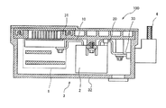
- FIG. 16 is a schematic cross-sectional view of the power converter 100 according to the sixth embodiment
- FIG. 17 is a schematic cross-sectional view of the power converter 100 showing the appearance of the smoothing capacitor 2.
- the elastic member 7 is sandwiched between the upper surface 231 of the smoothing capacitor 2 and the cover portion 32 of the housing 3, and the smoothing capacitor 2 and the housing 3 are bolted. It is different from the other embodiments in that they are not fastened.
- the elastic member 7 is sandwiched between the upper surface 231 of the smoothing capacitor 2 (capacitor case 23) and the upper portion 327 of the cover 32 of the housing 3.
- the elastic member 7 is made of an elastic material having better thermal conductivity than the capacitor case 23, and the lower surface 71 contacts the upper surface 231 of the smoothing capacitor 2 and the upper surface 72 contacts the inner surface of the upper portion 327 of the cover portion 32.
- the elastic member 7 regulates the vertical movement of the smoothing capacitor 2
- the bracket 24 of the smoothing capacitor 2 and the holding portion 318 of the base portion 31 are separated from each other. Not fastened with bolts, etc.
- the elastic member 7 may be a conductive member or an insulating member as long as it is an elastic material having good thermal conductivity.
- the upper surface 231 of the smoothing capacitor 2 is in contact with the cover portion 32 of the housing 3 via the elastic member 7.
- the vertical movement of the smoothing capacitor 2 is restricted, and it is not necessary to fasten the capacitor case 23 of the smoothing capacitor 2 and the base portion 31 of the housing 3 with a bolt or the like. Therefore, the takt time at the time of manufacturing can be shortened.
- the elastic member 7 interposed between the smoothing capacitor 2 and the cover portion 32 of the housing 3 is made of an elastic material having better thermal conductivity than the capacitor case 23. Therefore, the heat of the smoothing capacitor 2 can be dissipated from the elastic member 7 to the cover portion 32 made of a metal material, and the temperature rise of the smoothing capacitor 2 can be suppressed.
- the mounting direction of the power conversion device 100 does not necessarily need to arrange the base portion 31 of the housing 3 on the lower side, and may be freely set according to the layout of the vehicle in which the power conversion device 100 is mounted. It may be arranged in any direction.
- the power converter 100 shown in FIG. 1 and the like may be installed upside down so that the base 31 is on the top and the cover 32 is on the bottom. May be installed in a tilted state.
- the cooling water is used as the cooling medium flowing through the cooling passage, but the cooling medium is not limited to this and may be, for example, a cooling medium gas.
Landscapes
- Engineering & Computer Science (AREA)
- Microelectronics & Electronic Packaging (AREA)
- Power Engineering (AREA)
- Physics & Mathematics (AREA)
- Thermal Sciences (AREA)
- Inverter Devices (AREA)
Abstract
L'invention concerne un dispositif de conversion de puissance électrique comprenant un onduleur constitué d'une pluralité de composants électriques, un condensateur de lissage qui lisse la puissance électrique, un boîtier dans lequel sont logés l'onduleur et le condensateur de lissage, et une première partie conductrice qui connecte le condensateur de lissage et l'onduleur. Le boîtier est formé d'un matériau résine, et est constitué d'une partie base sur laquelle sont placés l'onduleur et le condensateur de lissage, et d'une partie couvercle qui est destinée à être fixée à la partie base de manière à recouvrir l'onduleur et le condensateur de lissage. Le long d'une partie du chemin reliant le condensateur de lissage et l'onduleur, la première partie conductrice s'approche de la partie base du boîtier ou vient en contact avec elle.
Priority Applications (5)
| Application Number | Priority Date | Filing Date | Title |
|---|---|---|---|
| PCT/IB2019/000172 WO2020169998A1 (fr) | 2019-02-18 | 2019-02-18 | Dispositif de conversion de puissance électrique |
| CN201980089702.2A CN113330679A (zh) | 2019-02-18 | 2019-02-18 | 电力变换装置 |
| US17/431,227 US11839068B2 (en) | 2019-02-18 | 2019-02-18 | Electric power converter |
| JP2021501112A JP7140262B2 (ja) | 2019-02-18 | 2019-02-18 | 電力変換装置 |
| EP19915774.4A EP3930168A4 (fr) | 2019-02-18 | 2019-02-18 | Dispositif de conversion de puissance électrique |
Applications Claiming Priority (1)
| Application Number | Priority Date | Filing Date | Title |
|---|---|---|---|
| PCT/IB2019/000172 WO2020169998A1 (fr) | 2019-02-18 | 2019-02-18 | Dispositif de conversion de puissance électrique |
Publications (1)
| Publication Number | Publication Date |
|---|---|
| WO2020169998A1 true WO2020169998A1 (fr) | 2020-08-27 |
Family
ID=72144200
Family Applications (1)
| Application Number | Title | Priority Date | Filing Date |
|---|---|---|---|
| PCT/IB2019/000172 WO2020169998A1 (fr) | 2019-02-18 | 2019-02-18 | Dispositif de conversion de puissance électrique |
Country Status (5)
| Country | Link |
|---|---|
| US (1) | US11839068B2 (fr) |
| EP (1) | EP3930168A4 (fr) |
| JP (1) | JP7140262B2 (fr) |
| CN (1) | CN113330679A (fr) |
| WO (1) | WO2020169998A1 (fr) |
Families Citing this family (5)
| Publication number | Priority date | Publication date | Assignee | Title |
|---|---|---|---|---|
| CN112262525A (zh) * | 2018-07-03 | 2021-01-22 | 日产自动车株式会社 | 电力转换单元 |
| US11785737B2 (en) | 2022-01-20 | 2023-10-10 | Borg Warner Luxembourg Automotive Systems SA | Systems and methods for cooling electronic components of a vehicle |
| US11950398B2 (en) * | 2022-01-20 | 2024-04-02 | Borgwarner Luxembourg Automotive Systems Sa | Systems and methods for cooling electronic components of a vehicle |
| US11943903B2 (en) | 2022-01-20 | 2024-03-26 | Borgwarner Luxembourg Automotive Systems Sa | Systems and methods for cooling electronic components of a vehicle |
| FR3133005A1 (fr) * | 2022-02-23 | 2023-08-25 | Psa Automobiles Sa | Système électrique pour véhicule automobile |
Citations (3)
| Publication number | Priority date | Publication date | Assignee | Title |
|---|---|---|---|---|
| JP2003018864A (ja) * | 2001-04-25 | 2003-01-17 | Mitsubishi Electric Corp | コンデンサモジュールおよびそれを用いた半導体装置 |
| JP2008067546A (ja) * | 2006-09-08 | 2008-03-21 | Toyota Motor Corp | コンデンサの冷却構造およびその冷却構造を備えたモータ |
| JP2018121457A (ja) | 2017-01-26 | 2018-08-02 | 日立オートモティブシステムズ株式会社 | 電力変換装置 |
Family Cites Families (22)
| Publication number | Priority date | Publication date | Assignee | Title |
|---|---|---|---|---|
| JPH1189248A (ja) * | 1997-09-02 | 1999-03-30 | Denso Corp | 電力制御装置 |
| JP4038899B2 (ja) * | 1998-11-04 | 2008-01-30 | 株式会社デンソー | 電源平滑用コンデンサ搭載型インバータ装置 |
| JP2002170739A (ja) * | 2000-11-29 | 2002-06-14 | Murata Mfg Co Ltd | 積層セラミックコンデンサモジュール |
| JP4538359B2 (ja) * | 2005-03-31 | 2010-09-08 | 株式会社日立産機システム | 電気回路モジュール |
| JP4756935B2 (ja) * | 2005-06-29 | 2011-08-24 | 本田技研工業株式会社 | コンデンサ搭載型インバータユニット |
| JP4848187B2 (ja) * | 2006-01-17 | 2011-12-28 | 日立オートモティブシステムズ株式会社 | 電力変換装置 |
| JP4461120B2 (ja) * | 2006-06-26 | 2010-05-12 | 日立オートモティブシステムズ株式会社 | インバータ駆動回転機システム及びそれを用いる電動車両 |
| JP2009095152A (ja) * | 2007-10-10 | 2009-04-30 | Fuji Electric Systems Co Ltd | 電力変換装置 |
| JP4638923B2 (ja) * | 2008-03-31 | 2011-02-23 | 日立オートモティブシステムズ株式会社 | 制御装置 |
| DE112011101365T5 (de) * | 2010-04-19 | 2013-03-28 | Toyota Jidosha K.K. | Element, das elektronische Komponenten enthält, und Energiewandlungsvorrichtung |
| JP5351107B2 (ja) * | 2010-07-23 | 2013-11-27 | 三菱電機株式会社 | コンデンサの冷却構造およびインバータ装置 |
| JP5733945B2 (ja) * | 2010-10-15 | 2015-06-10 | 三菱重工業株式会社 | インバータモジュールおよびインバータ一体型電動圧縮機 |
| JP5879726B2 (ja) * | 2011-04-11 | 2016-03-08 | 富士電機株式会社 | インバータ装置 |
| JP5174936B2 (ja) * | 2011-05-19 | 2013-04-03 | 日立オートモティブシステムズ株式会社 | 電力変換装置 |
| JP5504219B2 (ja) * | 2011-07-27 | 2014-05-28 | 日立オートモティブシステムズ株式会社 | 電力変換装置 |
| JP5975916B2 (ja) * | 2013-03-22 | 2016-08-23 | 株式会社日立製作所 | コンデンサ装置および電力変換装置 |
| JP6161550B2 (ja) * | 2014-02-05 | 2017-07-12 | 日立オートモティブシステムズ株式会社 | 電力変換装置 |
| US9615490B2 (en) * | 2014-05-15 | 2017-04-04 | Lear Corporation | Coldplate with integrated DC link capacitor for cooling thereof |
| JP6455523B2 (ja) * | 2014-12-22 | 2019-01-23 | 株式会社村田製作所 | コンデンサ回路、コンデンサモジュールおよび電力変換システム |
| GB2542468B (en) * | 2015-07-22 | 2017-12-13 | Lear Corp | Coldplate with integrated DC link capacitor for cooling thereof |
| MX2018012986A (es) * | 2016-04-28 | 2019-01-28 | Nissan Motor | Dispositivo de conversion de energia en vehiculo. |
| CN109873567B (zh) * | 2017-12-04 | 2022-02-25 | 株式会社电装 | 电力变换装置 |
-
2019
- 2019-02-18 US US17/431,227 patent/US11839068B2/en active Active
- 2019-02-18 EP EP19915774.4A patent/EP3930168A4/fr active Pending
- 2019-02-18 WO PCT/IB2019/000172 patent/WO2020169998A1/fr unknown
- 2019-02-18 JP JP2021501112A patent/JP7140262B2/ja active Active
- 2019-02-18 CN CN201980089702.2A patent/CN113330679A/zh active Pending
Patent Citations (3)
| Publication number | Priority date | Publication date | Assignee | Title |
|---|---|---|---|---|
| JP2003018864A (ja) * | 2001-04-25 | 2003-01-17 | Mitsubishi Electric Corp | コンデンサモジュールおよびそれを用いた半導体装置 |
| JP2008067546A (ja) * | 2006-09-08 | 2008-03-21 | Toyota Motor Corp | コンデンサの冷却構造およびその冷却構造を備えたモータ |
| JP2018121457A (ja) | 2017-01-26 | 2018-08-02 | 日立オートモティブシステムズ株式会社 | 電力変換装置 |
Also Published As
| Publication number | Publication date |
|---|---|
| JPWO2020169998A1 (fr) | 2020-08-27 |
| JP7140262B2 (ja) | 2022-09-21 |
| EP3930168A4 (fr) | 2022-03-02 |
| CN113330679A (zh) | 2021-08-31 |
| EP3930168A1 (fr) | 2021-12-29 |
| US20220142014A1 (en) | 2022-05-05 |
| US11839068B2 (en) | 2023-12-05 |
Similar Documents
| Publication | Publication Date | Title |
|---|---|---|
| WO2020169998A1 (fr) | Dispositif de conversion de puissance électrique | |
| US10178754B2 (en) | Circuit board module and electronic device | |
| JP5737275B2 (ja) | インバータ装置 | |
| JP2004190547A (ja) | インバータ一体型電動コンプレッサ及びその組み立て方法 | |
| CN108293311B (zh) | 电气接线盒 | |
| JP7429935B2 (ja) | 電力変換装置及び車両 | |
| JP6929813B2 (ja) | パワー半導体装置 | |
| JP4023054B2 (ja) | 電子回路ユニット | |
| KR102458738B1 (ko) | 커패시터 직접냉각방식의 인버터 | |
| JP7282265B2 (ja) | 電力変換装置 | |
| JP2019013079A (ja) | パワー半導体装置及びそれを用いた電力変換装置 | |
| JP2001298290A (ja) | 電子ユニットボックスの放熱構造 | |
| JP5973833B2 (ja) | パワー半導体モジュール | |
| US11770915B2 (en) | Electrical equipment comprising a busbar cooled by two faces of a heatsink | |
| CN111465258B (zh) | 用于电子单元的导热插入元件 | |
| CN211210224U (zh) | 一种在输出端背面散热的全密封金属外壳 | |
| WO2020080248A1 (fr) | Structure de circuit et boîte de jonction électrique | |
| CN113853075A (zh) | 具有构成承载结构的散热器芯件的组件 | |
| KR20030063178A (ko) | 전기 장치 | |
| JP2021158208A (ja) | 電子モジュール | |
| KR102361530B1 (ko) | 캐패시터 직접냉각방식의 인버터 | |
| CN218587504U (zh) | 电助力自行车控制器 | |
| JP2000091778A (ja) | 箱体の冷却構造及び冷却方法 | |
| WO2023243207A1 (fr) | Module semi-conducteur et dispositif de conversion de puissance | |
| WO2023037523A1 (fr) | Dispositif de conversion de puissance |
Legal Events
| Date | Code | Title | Description |
|---|---|---|---|
| 121 | Ep: the epo has been informed by wipo that ep was designated in this application |
Ref document number: 19915774 Country of ref document: EP Kind code of ref document: A1 |
|
| ENP | Entry into the national phase |
Ref document number: 2021501112 Country of ref document: JP Kind code of ref document: A |
|
| NENP | Non-entry into the national phase |
Ref country code: DE |
|
| ENP | Entry into the national phase |
Ref document number: 2019915774 Country of ref document: EP Effective date: 20210920 |