WO2019211988A1 - コンタクト - Google Patents
コンタクト Download PDFInfo
- Publication number
- WO2019211988A1 WO2019211988A1 PCT/JP2019/016565 JP2019016565W WO2019211988A1 WO 2019211988 A1 WO2019211988 A1 WO 2019211988A1 JP 2019016565 W JP2019016565 W JP 2019016565W WO 2019211988 A1 WO2019211988 A1 WO 2019211988A1
- Authority
- WO
- WIPO (PCT)
- Prior art keywords
- contact
- base
- base portion
- joint surface
- parallel
- Prior art date
- Legal status (The legal status is an assumption and is not a legal conclusion. Google has not performed a legal analysis and makes no representation as to the accuracy of the status listed.)
- Ceased
Links
Images


Classifications
-
- H—ELECTRICITY
- H01—ELECTRIC ELEMENTS
- H01R—ELECTRICALLY-CONDUCTIVE CONNECTIONS; STRUCTURAL ASSOCIATIONS OF A PLURALITY OF MUTUALLY-INSULATED ELECTRICAL CONNECTING ELEMENTS; COUPLING DEVICES; CURRENT COLLECTORS
- H01R4/00—Electrically-conductive connections between two or more conductive members in direct contact, i.e. touching one another; Means for effecting or maintaining such contact; Electrically-conductive connections having two or more spaced connecting locations for conductors and using contact members penetrating insulation
- H01R4/02—Soldered or welded connections
- H01R4/028—Soldered or welded connections comprising means for preventing flowing or wicking of solder or flux in parts not desired
-
- H—ELECTRICITY
- H01—ELECTRIC ELEMENTS
- H01R—ELECTRICALLY-CONDUCTIVE CONNECTIONS; STRUCTURAL ASSOCIATIONS OF A PLURALITY OF MUTUALLY-INSULATED ELECTRICAL CONNECTING ELEMENTS; COUPLING DEVICES; CURRENT COLLECTORS
- H01R12/00—Structural associations of a plurality of mutually-insulated electrical connecting elements, specially adapted for printed circuits, e.g. printed circuit boards [PCB], flat or ribbon cables, or like generally planar structures, e.g. terminal strips, terminal blocks; Coupling devices specially adapted for printed circuits, flat or ribbon cables, or like generally planar structures; Terminals specially adapted for contact with, or insertion into, printed circuits, flat or ribbon cables, or like generally planar structures
- H01R12/50—Fixed connections
- H01R12/51—Fixed connections for rigid printed circuits or like structures
- H01R12/55—Fixed connections for rigid printed circuits or like structures characterised by the terminals
- H01R12/57—Fixed connections for rigid printed circuits or like structures characterised by the terminals surface mounting terminals
-
- H—ELECTRICITY
- H01—ELECTRIC ELEMENTS
- H01R—ELECTRICALLY-CONDUCTIVE CONNECTIONS; STRUCTURAL ASSOCIATIONS OF A PLURALITY OF MUTUALLY-INSULATED ELECTRICAL CONNECTING ELEMENTS; COUPLING DEVICES; CURRENT COLLECTORS
- H01R13/00—Details of coupling devices of the kinds covered by groups H01R12/70 or H01R24/00 - H01R33/00
- H01R13/02—Contact members
- H01R13/22—Contacts for co-operating by abutting
- H01R13/24—Contacts for co-operating by abutting resilient; resiliently-mounted
- H01R13/2442—Contacts for co-operating by abutting resilient; resiliently-mounted with a single cantilevered beam
-
- H—ELECTRICITY
- H01—ELECTRIC ELEMENTS
- H01R—ELECTRICALLY-CONDUCTIVE CONNECTIONS; STRUCTURAL ASSOCIATIONS OF A PLURALITY OF MUTUALLY-INSULATED ELECTRICAL CONNECTING ELEMENTS; COUPLING DEVICES; CURRENT COLLECTORS
- H01R4/00—Electrically-conductive connections between two or more conductive members in direct contact, i.e. touching one another; Means for effecting or maintaining such contact; Electrically-conductive connections having two or more spaced connecting locations for conductors and using contact members penetrating insulation
- H01R4/02—Soldered or welded connections
Definitions
- the present disclosure relates to a contact that is disposed between two members and electrically connects them.
- the contact that electrically connects the two members may be fixed to one member by soldering as described in Patent Document 1 below, for example.
- the contact Since it is difficult to make the distance between the two members completely constant, it has been attempted to connect the two members appropriately by configuring the contact to be elastically deformable. It is desirable that the range in which the contact can be elastically deformed is wide since the contact can be used for the two members having a large distance tolerance. In recent years, the density of parts mounted on a substrate has been increased to reduce the size of the device, and it is desirable that the contact be also reduced in size. However, if the size of a conventional contact is simply reduced, the elasticity decreases. The elastic deformation range is reduced.
- An object of the present disclosure is to provide a contact that can suppress a decrease in elasticity.
- One aspect of the present disclosure includes a thin plate member having elasticity and conductivity, is joined to the first member by soldering, and is disposed between the first member and the second member, and the first member is interposed via the thin plate member.
- a contact that electrically connects the member and the second member and includes a base portion and a movable portion.
- the base has a joint surface joined to the first member.
- the movable portion includes a contact portion that contacts the second member and a connecting portion that is connected to the base portion, and is configured to be elastically deformable with respect to the base portion.
- the connecting portion gradually moves away from the first member. In a predetermined range from the connection position with the base portion in the connection portion, the wettability of the solder is low as compared with the joint surface.
- connection part If it is such a structure, it will become difficult to solder a connection part, and it can control that the elastic deformation of a connection part is restricted by soldering, and it suppresses that the elasticity of the whole movable part falls. it can.
- the contact described above is provided in a position where the contact portion overlaps the base when the contact is projected onto a plane parallel to the bonding surface, and the length of the contact in the direction connecting the connecting portion and the contact portion.
- the thickness may be 2 mm or less.
- the above-mentioned base may be provided with a through hole that connects the joint surface to the surface on the back side of the joint surface.
- the movable part described above may include a parallel part parallel to the joint surface.
- the parallel part may be of a size that can be sucked by the suction nozzle.
- the contact can be arranged on the substrate or the like by automatic mounting using a suction nozzle.
- At least a part of the side surface of the base portion described above may have higher wettability on the side surface than the predetermined range described above. With such a configuration, the soldering is performed well on the side surface of the base portion, and the contact is hardly peeled off from the substrate or the like. Moreover, since the solder melted on the side surface of the base portion can easily flow, it is possible to more highly suppress the solder from adhering to the connecting portion.
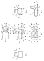
- FIG. 2A is a front view of the embodiment contact
- FIG. 2B is a right side view
- FIG. 2C is a left side view
- FIG. 2D is a plan view
- FIG. 2E is a bottom view
- FIG. FIG. 2B is a sectional view taken along the line IIF-IIF in FIG. 2E.
- FIG. 3B is a cross-sectional view taken along the line III-III of FIG. 2A and shows a state in which the contact is soldered to the first member. It is a front view which shows operation
- the contact 1 shown in FIGS. 1 and 2A to 2E is a contact that can be surface-mounted on an electronic board by an automatic mounting machine.
- the contact 1 comes into contact with the housing or other elements, and electrically connects them to the electronic substrate.
- the contact 1 is constituted by a thin plate member having elasticity and conductivity. For example, you may be comprised with the metal plate.
- Contact 1 includes a base portion 11 and a movable portion 12.
- the base 11 is a portion that can be brought into contact with the electronic substrate when the contact 1 is surface-mounted on the electronic substrate.
- the main part is flat form.
- the base 11 has a length in a direction from one end to the other end that is greater than a width direction intersecting the base 11.
- the configuration of the contact 1 will be described with the above-mentioned one as the left and the other as the right.
- the movable portion 12 extends from the left end portion of the base portion 11, is folded back toward the right end portion, and the extended tip is at a position facing the base portion 11.
- the main portion of the movable portion 12 is located above the base portion 11.
- the vertical and horizontal directions are merely used for convenience of explanation, and do not limit the usage mode of the contact 1.
- the base 11 includes a wide portion 21 having a relatively large length in the width direction, and a narrow portion 22 that is located on the right side of the wide portion 21 and is smaller in width than the wide portion 21.
- a through hole 23 is formed in the wide portion 21 so as to penetrate the base portion 11 in the thickness direction.
- the through-hole 23 includes a lower portion 23a and an upper portion 23b, and the shapes thereof are different.
- the lower part 23a is formed so that the hole diameter gradually increases toward the lower part, and the upper part 23b has the same hole diameter as the upper end of the lower part 23a, and the hole diameter does not change regardless of the vertical position.
- the diameter of the through hole 23 may be 0.2 mm at the upper part 23b and 0.3 mm at the lower end of the lower part 23a, for example.
- the wide portion 21 is formed with notches 24 at both ends in the width direction from the end in the width direction toward the center.
- the notch 24 is provided in the vicinity of the left end of the base 11 and at a position spaced from the left end.
- a pair of protective pieces 25 extending upward are provided at both ends of the narrow width portion 22 in the width direction.
- the base 11 has a bonding surface 26 that is a surface bonded to the electronic substrate by soldering.
- the lower surface of the wide portion 21 and the lower surface of the narrow portion 22 correspond to the joint surface 26. That is, the above-described through hole 23 is a hole connected from the joint surface 26 to the joint surface of the base 11 from the back surface (that is, the upper surface).
- the base portion 11 is formed with a first plating portion 27 that is subjected to a gold plating process for improving solder wettability.
- the first plated portion 27 is a portion indicated by hatching in FIGS. 2A and 2E, and the wide portion 21 in addition to the lower surface of the wide portion 21 and the lower surface of the narrow portion 22 (that is, the bonding surface 26). Also formed on the side surface of the narrow portion 22, the inner peripheral surface of the through hole 23, the inner wall surface of the notch 24, and the vicinity of the lower end portion outside the protective piece 25.
- the metal used as the 1st plating part 27 is not limited to gold
- FIG. 3 is a cross-sectional view showing the contact 1 soldered on the copper foil 4 provided on the electronic substrate 3.
- An electronic board is an example of the first member.
- Reference numeral 5 denotes a resist.
- the solder fillet 7 is also appropriately formed on the side surface of the wide portion 21 where the first plating portion 27 is formed and the inner peripheral surface of the through hole 23. Since the hole diameter of the lower portion 23a of the through hole 23 gradually increases downward, solder melted in the reflow furnace easily flows and spreads.
- the fillet 7 is also formed on the side surface other than the right end side of the narrow width portion 22 and the lower end portion of the protection piece 25. Further, the entire bonding surface 26 is bonded to the electronic substrate 3 by soldering.
- the movable portion 12 includes a connecting portion 31, a vertical portion 32, a parallel portion 33, an inclined portion 34, and a contact portion 35 in order from a portion adjacent to the base portion 11.
- a connecting portion 31 a vertical portion 32, a parallel portion 33, an inclined portion 34, and a contact portion 35 in order from a portion adjacent to the base portion 11.
- the connecting portion 31 is connected to the base portion 11 and bends and extends from the base portion 11 in a direction intersecting the joining surface 26.
- the connecting portion 31 is a portion that bends away from the electronic substrate 3 (or a virtual plane including the bonding surface 26) gradually in a state where the contact 1 is bonded to the electronic substrate 3.
- a vertical portion 32 extending in the vertical direction is connected to the upper end of the connecting portion 31.
- the parallel portion 33 extends rightward from the upper end of the vertical portion 32.
- the parallel portion 33 is parallel to the joint surface 26 of the base portion 11.
- the parallel portion 33 is used as a suction surface when the suction nozzle of the automatic mounting machine sucks 1. Therefore, the parallel part 33 is configured to have a size that can be sucked by the suction nozzle.
- the plane parallel to at least the wide part 21 and the narrow part 22 is good also as 0.6 mm or more about both the left-right direction and the width direction.
- the inclined portion 34 extends from the right end of the parallel portion 33 so as to be inclined to the upper right. Thereby, the contact portion 35 can be provided at a position away from the base portion 11.
- the contact portion 35 is provided at the upper end of the inclined portion 34 and has a curved surface shape that is wound downward from the viewpoint of FIG. 2A.
- This contact part 35 contacts the housing
- the housing 9 is an example of a second member.
- the inclined portion 34 and the contact portion 35 are shorter in the width direction than the connecting portion 31, the vertical portion 32, and the parallel portion 33.
- the width of the contact portion 35 may be 65% or less of the width of the wide portion 21 of the base portion 11.
- the movable part 12 is provided with a second plating part 37 plated with gold on at least the upper surface of the contact part 35.
- the movable portion 12 is a portion that is not fixed by soldering, but the second plating portion 37 is formed in order to enhance electrical conductivity with the housing 9.
- the non-bonding surface 42 that is a surface of the connecting portion 31 that faces the electronic substrate 3 and that is within a predetermined range from the connecting position 41 between the connecting portion 31 and the base portion 11.
- the plating process for forming gold plating for improving wettability is not performed. Therefore, the wettability of the non-joint surface 42 of the connection part 31 is lower than the wettability of the joint surface 26 and the like subjected to the gold plating process, thereby suppressing the connection part 31 from being soldered.
- the movable portion 12 is elastically deformed with respect to the base portion 11 when a load is applied downward in contact with the housing 9.
- the contact 1 is disposed between the electronic substrate 3 and the housing 9 and electrically connects the electronic substrate 3 and the housing 9 via the thin plate member.
- the connecting portion 31 is not soldered, the connecting portion 31 is also elastically deformed as compared with the case where it is temporarily soldered. Since the movable part 12 rotates about the connecting part 31 and elastically deforms, when the amount of displacement that can be deformed by the connecting part 31 increases, the range in which the movable part 12 can be elastically deformed is greatly improved. That is, the elasticity of the base 11 is improved.
- the pair of protective pieces 25 abut against the housing 9 when the housing 9 approaches the electronic substrate 3 excessively, and suppresses the housing 9 from approaching the electronic substrate 3 any more.
- the movable portion 12 is prevented from yielding and plastically deforming as a result of excessive displacement toward the base portion 11.
- the contact portion 35 is provided at a position overlapping the base portion 11. 2D, the length in the left-right direction of the contact 1 is 1.6 mm, and the length in the width direction is 0.8 mm.
- the manufacturing method of the contact 1 is not particularly limited, one example will be described.
- the coil material that is not plated is punched or bent by a press, unnecessary portions are extracted, and the shape of the contact 1 is subjected to bending. Forming a molded product. This formed product is kept in a state where it is connected to the carrier and the bridge to form a pressed coil material.
- a surface treatment is performed on the pressed coil material to form nickel plating that has an effect of inhibiting corrosion and is compatible with gold plating.
- gold plating to be the first plating portion 27 and the second plating portion 37 is formed at a position to be the bonding surface 26 and the contact portion 35.
- a wet plating method such as electroplating or a dry plating method such as sputtering can be used.
- a wet plating method such as electroplating or a dry plating method such as sputtering
- the wettability of the solder can be improved.
- the bridge was cut from the pressed coil material to form the contact 1. The cut surface of this bridge is the right end surface of the narrow portion 22 in the base 11.
- the gold plating of the connecting portion 31 may be removed by plasma treatment.
- the contact 1 of this embodiment can suppress the elastic deformation of the connection part 31 by soldering by making it difficult for the connection part 31 to be soldered, and thereby the elasticity of the movable part 12 whole. Reduction can be suppressed.
- the contact 1 of the embodiment has a length of 1.6 mm, and particularly in such a small contact, a decrease in elasticity can be suppressed.
- the contact 1 of the present embodiment can suppress the flow of solder melted in the direction of the connecting portion 31. Since the melted solder can flow into the through hole 23 and the notch 24, the amount of solder flowing outside the joint surface 26 is reduced. As a result, it is possible to more highly suppress solder from attaching to the connecting portion 31.
- the surface of the through hole 23 and the notch 24 is subjected to a gold plating process, the wettability is improved, and the above-described solder flow is promoted.
- the gold plating process is performed also on the side surface of the base portion 11, the solder is easy to adjust to the side surface, and an increase in the amount flowing to the connecting portion 31 can be suppressed, and the soldering between the contact 1 and the electronic substrate 3 is good.
- the contact 1 is less likely to be peeled off from the electronic substrate 3.
- the notch 24 is not provided so as to be hooked on the boundary portion between the base portion 11 and the connecting portion 31, that is, the connecting position 41. Therefore, the connecting portion 31 is connected to the base portion 11 over its entire width. In such a configuration, since the connecting portion 31 is firmly connected to the base portion 11, the risk of the connecting portion 31 being damaged when a load is applied to the movable portion 12 can be reduced.
- the suction nozzle of the automatic mounting machine can be sucked to the parallel portion 33. Therefore, the contact 1 can be arranged on the electronic substrate 3 by an automatic mounting machine.
- the contact 1 according to the present embodiment has a through-hole 23 and a notch 24, and when the solder is melted in the reflow furnace, the floating displacement is suppressed and the contact is made at an appropriate position on the electronic substrate 3. Self-alignment in which 1 moves can be expected.
- the non-joint surface 42 of the connection part 31 is provided in the left side in the base 11, and the non-joint surface 42 has low solder wettability. Therefore, a solder fillet is hardly formed between the left end of the base 11 and the electronic substrate 3.
- the end face on the right end face of the base 11, that is, the end face at the right end of the narrow width portion 22 is formed by performing a gold plating surface treatment on the metal plate material used as the material of the contact 1 and then cutting the end face, There is no gold-plated part on the cut surface. Therefore, it is difficult to form a fillet between the right end of the base 11 and the electronic substrate 3.
- the contact 1 is soldered by reflow, the contact 1 is less likely to be displaced by being pulled by the solder fillets formed on the left and right sides of the base 11, and can be soldered to an expected position. .
- the shape of the contact is not limited to the example shown in the above embodiment.
- any one or more of the through hole 23, the notch 24, and the protective piece 25 may not be provided.
- the through hole 23 may be a hole having no change in the hole diameter in the thickness direction of the base portion 11, or the hole diameter may be changed in the entire area in the thickness direction.
- the notch 24 may have a shape different from that of the above embodiment.
- the contact size is not particularly limited. Note that the use of the characteristics of the contact of the present disclosure is particularly effective for a contact having a length of 2 mm or less on the left and right sides.
- the contact 1 constituted by a conductive thin plate member is exemplified.
- the contact may include other elements such as a synthetic resin as long as the function of electrically connecting the two members is not lost.
- the position where surface treatment for wettability change such as gold plating is performed is not limited to the position shown in the above embodiment.
- the gold plating process may not be performed on a part of the region where the first plating portion 27 is formed, such as the side surface of the base portion 11 and the inner peripheral surface of the through hole 23.
- a part of the joint surface 26 that is not subjected to the gold plating process may exist.
- At least a part of the side surface of the base 11 may be configured to have higher solder wettability than the non-bonded surface 42.
- the gold plating process may be performed at a position other than the second plating portion 37 in the movable portion 12.
- the electronic substrate 3 is illustrated as an example of the first member, and the housing 9 is illustrated as an example of the second member.
- the first member and the second member are not limited to those illustrated.
- the first member may be a housing and the second member may be an electronic substrate.
Landscapes
- Coupling Device And Connection With Printed Circuit (AREA)
- Connections Effected By Soldering, Adhesion, Or Permanent Deformation (AREA)
- Contacts (AREA)
Priority Applications (3)
| Application Number | Priority Date | Filing Date | Title |
|---|---|---|---|
| EP19796536.1A EP3758153B1 (en) | 2018-05-02 | 2019-04-18 | Contact |
| CN201980022518.6A CN112437999B (zh) | 2018-05-02 | 2019-04-18 | 接触件 |
| US16/982,325 US11121494B2 (en) | 2018-05-02 | 2019-04-18 | Contact |
Applications Claiming Priority (2)
| Application Number | Priority Date | Filing Date | Title |
|---|---|---|---|
| JP2018-088795 | 2018-05-02 | ||
| JP2018088795A JP7076132B2 (ja) | 2018-05-02 | 2018-05-02 | コンタクト |
Publications (1)
| Publication Number | Publication Date |
|---|---|
| WO2019211988A1 true WO2019211988A1 (ja) | 2019-11-07 |
Family
ID=68386386
Family Applications (1)
| Application Number | Title | Priority Date | Filing Date |
|---|---|---|---|
| PCT/JP2019/016565 Ceased WO2019211988A1 (ja) | 2018-05-02 | 2019-04-18 | コンタクト |
Country Status (5)
| Country | Link |
|---|---|
| US (1) | US11121494B2 (https=) |
| EP (1) | EP3758153B1 (https=) |
| JP (1) | JP7076132B2 (https=) |
| CN (1) | CN112437999B (https=) |
| WO (1) | WO2019211988A1 (https=) |
Families Citing this family (1)
| Publication number | Priority date | Publication date | Assignee | Title |
|---|---|---|---|---|
| CN215266745U (zh) * | 2020-12-29 | 2021-12-21 | 番禺得意精密电子工业有限公司 | 连接器组件 |
Citations (6)
| Publication number | Priority date | Publication date | Assignee | Title |
|---|---|---|---|---|
| US6065980A (en) * | 1998-06-29 | 2000-05-23 | Cisco Technology, Inc. | Grounding a PCB to an enclosure sub-assembly using a grounding spring |
| JP2001217535A (ja) | 2000-01-31 | 2001-08-10 | Kitagawa Ind Co Ltd | 導電部材 |
| EP1381116A1 (en) * | 2002-07-11 | 2004-01-14 | Itt Manufacturing Enterprises, Inc. | Sprung electrical terminal |
| JP2006208062A (ja) * | 2005-01-26 | 2006-08-10 | Alps Electric Co Ltd | 接点部材及び、前記接点部材を用いた接点シート、接点基板、ならびに電子機器ユニット |
| JP2010161010A (ja) * | 2009-01-09 | 2010-07-22 | Kitagawa Ind Co Ltd | コンタクト |
| JP2013073882A (ja) * | 2011-09-29 | 2013-04-22 | Shinko Electric Ind Co Ltd | スプリング端子付配線基板及びその実装構造とソケット |
Family Cites Families (13)
| Publication number | Priority date | Publication date | Assignee | Title |
|---|---|---|---|---|
| JPS58178282U (ja) | 1982-05-21 | 1983-11-29 | 三菱電機株式会社 | 電気部品のろう付端子 |
| JP2529849Y2 (ja) * | 1990-12-25 | 1997-03-19 | ヒロセ電機株式会社 | 表面実装用コネクタの補強金具構造 |
| JPH08248435A (ja) * | 1995-03-14 | 1996-09-27 | Hitachi Ltd | 電子部品およびこの電子部品を用いた液晶表示モジュール |
| JP3064756U (ja) | 1999-06-10 | 2000-01-21 | トーマス アンド ベッツ インターナショナル,インク. | ア―ス用端子 |
| SG99960A1 (en) * | 2001-11-23 | 2003-11-27 | Fci Asia Technology Pte Ltd | Electrical connector |
| JP4482533B2 (ja) | 2006-03-15 | 2010-06-16 | 北川工業株式会社 | コンタクト部材 |
| JP4905983B2 (ja) | 2007-10-03 | 2012-03-28 | 北川工業株式会社 | 表面実装コンタクト |
| JP4887412B2 (ja) * | 2009-09-18 | 2012-02-29 | ヒロセ電機株式会社 | 回路基板用電気コネクタ |
| US8206188B1 (en) * | 2010-12-28 | 2012-06-26 | Cheng Uei Precision Industry Co., Ltd. | Connector terminal |
| KR101165558B1 (ko) * | 2012-01-04 | 2012-07-16 | 강태석 | 컨텍터 |
| JP5927607B2 (ja) | 2012-03-15 | 2016-06-01 | 北川工業株式会社 | コンタクト部材 |
| US10707627B2 (en) * | 2017-09-29 | 2020-07-07 | Apple Inc. | Hybrid connector |
| US10910748B2 (en) * | 2017-11-13 | 2021-02-02 | Te Connectivity Corporation | Cable socket connector assembly for an electronic |
-
2018
- 2018-05-02 JP JP2018088795A patent/JP7076132B2/ja active Active
-
2019
- 2019-04-18 US US16/982,325 patent/US11121494B2/en active Active
- 2019-04-18 WO PCT/JP2019/016565 patent/WO2019211988A1/ja not_active Ceased
- 2019-04-18 CN CN201980022518.6A patent/CN112437999B/zh active Active
- 2019-04-18 EP EP19796536.1A patent/EP3758153B1/en active Active
Patent Citations (6)
| Publication number | Priority date | Publication date | Assignee | Title |
|---|---|---|---|---|
| US6065980A (en) * | 1998-06-29 | 2000-05-23 | Cisco Technology, Inc. | Grounding a PCB to an enclosure sub-assembly using a grounding spring |
| JP2001217535A (ja) | 2000-01-31 | 2001-08-10 | Kitagawa Ind Co Ltd | 導電部材 |
| EP1381116A1 (en) * | 2002-07-11 | 2004-01-14 | Itt Manufacturing Enterprises, Inc. | Sprung electrical terminal |
| JP2006208062A (ja) * | 2005-01-26 | 2006-08-10 | Alps Electric Co Ltd | 接点部材及び、前記接点部材を用いた接点シート、接点基板、ならびに電子機器ユニット |
| JP2010161010A (ja) * | 2009-01-09 | 2010-07-22 | Kitagawa Ind Co Ltd | コンタクト |
| JP2013073882A (ja) * | 2011-09-29 | 2013-04-22 | Shinko Electric Ind Co Ltd | スプリング端子付配線基板及びその実装構造とソケット |
Non-Patent Citations (1)
| Title |
|---|
| See also references of EP3758153A4 |
Also Published As
| Publication number | Publication date |
|---|---|
| US20210013658A1 (en) | 2021-01-14 |
| JP2019194956A (ja) | 2019-11-07 |
| EP3758153A1 (en) | 2020-12-30 |
| CN112437999A (zh) | 2021-03-02 |
| US11121494B2 (en) | 2021-09-14 |
| CN112437999B (zh) | 2022-08-23 |
| EP3758153B1 (en) | 2024-11-20 |
| JP7076132B2 (ja) | 2022-05-27 |
| EP3758153A4 (en) | 2021-11-10 |
Similar Documents
| Publication | Publication Date | Title |
|---|---|---|
| KR101185351B1 (ko) | 커넥터 | |
| JP5472272B2 (ja) | 同軸コネクタプラグ及びその製造方法 | |
| US10403990B2 (en) | Press-fit terminal and electronic device | |
| CN216698775U (zh) | 用于将基板连接在一起的电触头及包括其的电学组件 | |
| JP2003142174A (ja) | 導電部材 | |
| JP7090622B2 (ja) | フレキシブルプリント配線板 | |
| WO2016199832A1 (ja) | 接触部材 | |
| JP7367154B2 (ja) | 半導体装置 | |
| CN104756321A (zh) | 连接器结构、母连接器以及公连接器 | |
| CN111262069A (zh) | 导电端子 | |
| JP6379416B2 (ja) | 接触部材 | |
| JP6398354B2 (ja) | コネクタ | |
| JP7507567B2 (ja) | プラグコネクター | |
| EP3226355A1 (en) | Contact | |
| JP6561805B2 (ja) | 基板用コネクタ | |
| CN111262063B (zh) | 导电端子、导电端子制造方法以及端子料带结构 | |
| JP5479406B2 (ja) | コネクタ | |
| US9570827B2 (en) | Contact member | |
| KR20130036060A (ko) | 회로 기판에 실장되는 부품의 고정금구 | |
| WO2019211988A1 (ja) | コンタクト | |
| JP7561499B2 (ja) | プラグコネクター | |
| JP5927607B2 (ja) | コンタクト部材 | |
| TWM512205U (zh) | 電接觸件及可熔元件 | |
| KR101005767B1 (ko) | 전기적 접속을 위한 핀 | |
| CN109417235B (zh) | 连接器 |
Legal Events
| Date | Code | Title | Description |
|---|---|---|---|
| 121 | Ep: the epo has been informed by wipo that ep was designated in this application |
Ref document number: 19796536 Country of ref document: EP Kind code of ref document: A1 |
|
| DPE1 | Request for preliminary examination filed after expiration of 19th month from priority date (pct application filed from 20040101) | ||
| ENP | Entry into the national phase |
Ref document number: 2019796536 Country of ref document: EP Effective date: 20200921 |
|
| NENP | Non-entry into the national phase |
Ref country code: DE |