WO2019211988A1 - Contact - Google Patents
Contact Download PDFInfo
- Publication number
- WO2019211988A1 WO2019211988A1 PCT/JP2019/016565 JP2019016565W WO2019211988A1 WO 2019211988 A1 WO2019211988 A1 WO 2019211988A1 JP 2019016565 W JP2019016565 W JP 2019016565W WO 2019211988 A1 WO2019211988 A1 WO 2019211988A1
- Authority
- WO
- WIPO (PCT)
- Prior art keywords
- contact
- base
- base portion
- joint surface
- parallel
- Prior art date
Links
- 229910000679 solder Inorganic materials 0.000 claims abstract description 25
- 238000005476 soldering Methods 0.000 claims abstract description 12
- 238000005304 joining Methods 0.000 claims abstract description 5
- 238000007747 plating Methods 0.000 description 36
- 239000000758 substrate Substances 0.000 description 28
- 239000010931 gold Substances 0.000 description 21
- 229910052737 gold Inorganic materials 0.000 description 21
- PCHJSUWPFVWCPO-UHFFFAOYSA-N gold Chemical compound [Au] PCHJSUWPFVWCPO-UHFFFAOYSA-N 0.000 description 20
- 238000000034 method Methods 0.000 description 12
- 239000000463 material Substances 0.000 description 6
- 239000002184 metal Substances 0.000 description 5
- 229910052751 metal Inorganic materials 0.000 description 5
- 238000004381 surface treatment Methods 0.000 description 5
- 230000007423 decrease Effects 0.000 description 4
- 230000000694 effects Effects 0.000 description 4
- 230000001681 protective effect Effects 0.000 description 4
- 238000006073 displacement reaction Methods 0.000 description 3
- 230000005489 elastic deformation Effects 0.000 description 3
- 238000004519 manufacturing process Methods 0.000 description 3
- 230000002093 peripheral effect Effects 0.000 description 3
- RYGMFSIKBFXOCR-UHFFFAOYSA-N Copper Chemical compound [Cu] RYGMFSIKBFXOCR-UHFFFAOYSA-N 0.000 description 2
- PXHVJJICTQNCMI-UHFFFAOYSA-N Nickel Chemical compound [Ni] PXHVJJICTQNCMI-UHFFFAOYSA-N 0.000 description 2
- 239000011889 copper foil Substances 0.000 description 2
- 238000013459 approach Methods 0.000 description 1
- 238000005452 bending Methods 0.000 description 1
- 238000005260 corrosion Methods 0.000 description 1
- 230000007797 corrosion Effects 0.000 description 1
- 238000005520 cutting process Methods 0.000 description 1
- 238000009713 electroplating Methods 0.000 description 1
- 150000002343 gold Chemical class 0.000 description 1
- 230000012447 hatching Effects 0.000 description 1
- 230000002401 inhibitory effect Effects 0.000 description 1
- 229910052759 nickel Inorganic materials 0.000 description 1
- 238000009832 plasma treatment Methods 0.000 description 1
- 238000003672 processing method Methods 0.000 description 1
- 238000004544 sputter deposition Methods 0.000 description 1
- 229920003002 synthetic resin Polymers 0.000 description 1
- 239000000057 synthetic resin Substances 0.000 description 1
Images


Classifications
-
- H—ELECTRICITY
- H01—ELECTRIC ELEMENTS
- H01R—ELECTRICALLY-CONDUCTIVE CONNECTIONS; STRUCTURAL ASSOCIATIONS OF A PLURALITY OF MUTUALLY-INSULATED ELECTRICAL CONNECTING ELEMENTS; COUPLING DEVICES; CURRENT COLLECTORS
- H01R4/00—Electrically-conductive connections between two or more conductive members in direct contact, i.e. touching one another; Means for effecting or maintaining such contact; Electrically-conductive connections having two or more spaced connecting locations for conductors and using contact members penetrating insulation
- H01R4/02—Soldered or welded connections
- H01R4/028—Soldered or welded connections comprising means for preventing flowing or wicking of solder or flux in parts not desired
-
- H—ELECTRICITY
- H01—ELECTRIC ELEMENTS
- H01R—ELECTRICALLY-CONDUCTIVE CONNECTIONS; STRUCTURAL ASSOCIATIONS OF A PLURALITY OF MUTUALLY-INSULATED ELECTRICAL CONNECTING ELEMENTS; COUPLING DEVICES; CURRENT COLLECTORS
- H01R12/00—Structural associations of a plurality of mutually-insulated electrical connecting elements, specially adapted for printed circuits, e.g. printed circuit boards [PCB], flat or ribbon cables, or like generally planar structures, e.g. terminal strips, terminal blocks; Coupling devices specially adapted for printed circuits, flat or ribbon cables, or like generally planar structures; Terminals specially adapted for contact with, or insertion into, printed circuits, flat or ribbon cables, or like generally planar structures
- H01R12/50—Fixed connections
- H01R12/51—Fixed connections for rigid printed circuits or like structures
- H01R12/55—Fixed connections for rigid printed circuits or like structures characterised by the terminals
- H01R12/57—Fixed connections for rigid printed circuits or like structures characterised by the terminals surface mounting terminals
-
- H—ELECTRICITY
- H01—ELECTRIC ELEMENTS
- H01R—ELECTRICALLY-CONDUCTIVE CONNECTIONS; STRUCTURAL ASSOCIATIONS OF A PLURALITY OF MUTUALLY-INSULATED ELECTRICAL CONNECTING ELEMENTS; COUPLING DEVICES; CURRENT COLLECTORS
- H01R13/00—Details of coupling devices of the kinds covered by groups H01R12/70 or H01R24/00 - H01R33/00
- H01R13/02—Contact members
- H01R13/22—Contacts for co-operating by abutting
- H01R13/24—Contacts for co-operating by abutting resilient; resiliently-mounted
- H01R13/2442—Contacts for co-operating by abutting resilient; resiliently-mounted with a single cantilevered beam
-
- H—ELECTRICITY
- H01—ELECTRIC ELEMENTS
- H01R—ELECTRICALLY-CONDUCTIVE CONNECTIONS; STRUCTURAL ASSOCIATIONS OF A PLURALITY OF MUTUALLY-INSULATED ELECTRICAL CONNECTING ELEMENTS; COUPLING DEVICES; CURRENT COLLECTORS
- H01R4/00—Electrically-conductive connections between two or more conductive members in direct contact, i.e. touching one another; Means for effecting or maintaining such contact; Electrically-conductive connections having two or more spaced connecting locations for conductors and using contact members penetrating insulation
- H01R4/02—Soldered or welded connections
Definitions
- the present disclosure relates to a contact that is disposed between two members and electrically connects them.
- the contact that electrically connects the two members may be fixed to one member by soldering as described in Patent Document 1 below, for example.
- the contact Since it is difficult to make the distance between the two members completely constant, it has been attempted to connect the two members appropriately by configuring the contact to be elastically deformable. It is desirable that the range in which the contact can be elastically deformed is wide since the contact can be used for the two members having a large distance tolerance. In recent years, the density of parts mounted on a substrate has been increased to reduce the size of the device, and it is desirable that the contact be also reduced in size. However, if the size of a conventional contact is simply reduced, the elasticity decreases. The elastic deformation range is reduced.
- An object of the present disclosure is to provide a contact that can suppress a decrease in elasticity.
- One aspect of the present disclosure includes a thin plate member having elasticity and conductivity, is joined to the first member by soldering, and is disposed between the first member and the second member, and the first member is interposed via the thin plate member.
- a contact that electrically connects the member and the second member and includes a base portion and a movable portion.
- the base has a joint surface joined to the first member.
- the movable portion includes a contact portion that contacts the second member and a connecting portion that is connected to the base portion, and is configured to be elastically deformable with respect to the base portion.
- the connecting portion gradually moves away from the first member. In a predetermined range from the connection position with the base portion in the connection portion, the wettability of the solder is low as compared with the joint surface.
- connection part If it is such a structure, it will become difficult to solder a connection part, and it can control that the elastic deformation of a connection part is restricted by soldering, and it suppresses that the elasticity of the whole movable part falls. it can.
- the contact described above is provided in a position where the contact portion overlaps the base when the contact is projected onto a plane parallel to the bonding surface, and the length of the contact in the direction connecting the connecting portion and the contact portion.
- the thickness may be 2 mm or less.
- the above-mentioned base may be provided with a through hole that connects the joint surface to the surface on the back side of the joint surface.
- the movable part described above may include a parallel part parallel to the joint surface.
- the parallel part may be of a size that can be sucked by the suction nozzle.
- the contact can be arranged on the substrate or the like by automatic mounting using a suction nozzle.
- At least a part of the side surface of the base portion described above may have higher wettability on the side surface than the predetermined range described above. With such a configuration, the soldering is performed well on the side surface of the base portion, and the contact is hardly peeled off from the substrate or the like. Moreover, since the solder melted on the side surface of the base portion can easily flow, it is possible to more highly suppress the solder from adhering to the connecting portion.
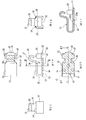
- FIG. 2A is a front view of the embodiment contact
- FIG. 2B is a right side view
- FIG. 2C is a left side view
- FIG. 2D is a plan view
- FIG. 2E is a bottom view
- FIG. FIG. 2B is a sectional view taken along the line IIF-IIF in FIG. 2E.
- FIG. 3B is a cross-sectional view taken along the line III-III of FIG. 2A and shows a state in which the contact is soldered to the first member. It is a front view which shows operation
- the contact 1 shown in FIGS. 1 and 2A to 2E is a contact that can be surface-mounted on an electronic board by an automatic mounting machine.
- the contact 1 comes into contact with the housing or other elements, and electrically connects them to the electronic substrate.
- the contact 1 is constituted by a thin plate member having elasticity and conductivity. For example, you may be comprised with the metal plate.
- Contact 1 includes a base portion 11 and a movable portion 12.
- the base 11 is a portion that can be brought into contact with the electronic substrate when the contact 1 is surface-mounted on the electronic substrate.
- the main part is flat form.
- the base 11 has a length in a direction from one end to the other end that is greater than a width direction intersecting the base 11.
- the configuration of the contact 1 will be described with the above-mentioned one as the left and the other as the right.
- the movable portion 12 extends from the left end portion of the base portion 11, is folded back toward the right end portion, and the extended tip is at a position facing the base portion 11.
- the main portion of the movable portion 12 is located above the base portion 11.
- the vertical and horizontal directions are merely used for convenience of explanation, and do not limit the usage mode of the contact 1.
- the base 11 includes a wide portion 21 having a relatively large length in the width direction, and a narrow portion 22 that is located on the right side of the wide portion 21 and is smaller in width than the wide portion 21.
- a through hole 23 is formed in the wide portion 21 so as to penetrate the base portion 11 in the thickness direction.
- the through-hole 23 includes a lower portion 23a and an upper portion 23b, and the shapes thereof are different.
- the lower part 23a is formed so that the hole diameter gradually increases toward the lower part, and the upper part 23b has the same hole diameter as the upper end of the lower part 23a, and the hole diameter does not change regardless of the vertical position.
- the diameter of the through hole 23 may be 0.2 mm at the upper part 23b and 0.3 mm at the lower end of the lower part 23a, for example.
- the wide portion 21 is formed with notches 24 at both ends in the width direction from the end in the width direction toward the center.
- the notch 24 is provided in the vicinity of the left end of the base 11 and at a position spaced from the left end.
- a pair of protective pieces 25 extending upward are provided at both ends of the narrow width portion 22 in the width direction.
- the base 11 has a bonding surface 26 that is a surface bonded to the electronic substrate by soldering.
- the lower surface of the wide portion 21 and the lower surface of the narrow portion 22 correspond to the joint surface 26. That is, the above-described through hole 23 is a hole connected from the joint surface 26 to the joint surface of the base 11 from the back surface (that is, the upper surface).
- the base portion 11 is formed with a first plating portion 27 that is subjected to a gold plating process for improving solder wettability.
- the first plated portion 27 is a portion indicated by hatching in FIGS. 2A and 2E, and the wide portion 21 in addition to the lower surface of the wide portion 21 and the lower surface of the narrow portion 22 (that is, the bonding surface 26). Also formed on the side surface of the narrow portion 22, the inner peripheral surface of the through hole 23, the inner wall surface of the notch 24, and the vicinity of the lower end portion outside the protective piece 25.
- the metal used as the 1st plating part 27 is not limited to gold
- FIG. 3 is a cross-sectional view showing the contact 1 soldered on the copper foil 4 provided on the electronic substrate 3.
- An electronic board is an example of the first member.
- Reference numeral 5 denotes a resist.
- the solder fillet 7 is also appropriately formed on the side surface of the wide portion 21 where the first plating portion 27 is formed and the inner peripheral surface of the through hole 23. Since the hole diameter of the lower portion 23a of the through hole 23 gradually increases downward, solder melted in the reflow furnace easily flows and spreads.
- the fillet 7 is also formed on the side surface other than the right end side of the narrow width portion 22 and the lower end portion of the protection piece 25. Further, the entire bonding surface 26 is bonded to the electronic substrate 3 by soldering.
- the movable portion 12 includes a connecting portion 31, a vertical portion 32, a parallel portion 33, an inclined portion 34, and a contact portion 35 in order from a portion adjacent to the base portion 11.
- a connecting portion 31 a vertical portion 32, a parallel portion 33, an inclined portion 34, and a contact portion 35 in order from a portion adjacent to the base portion 11.
- the connecting portion 31 is connected to the base portion 11 and bends and extends from the base portion 11 in a direction intersecting the joining surface 26.
- the connecting portion 31 is a portion that bends away from the electronic substrate 3 (or a virtual plane including the bonding surface 26) gradually in a state where the contact 1 is bonded to the electronic substrate 3.
- a vertical portion 32 extending in the vertical direction is connected to the upper end of the connecting portion 31.
- the parallel portion 33 extends rightward from the upper end of the vertical portion 32.
- the parallel portion 33 is parallel to the joint surface 26 of the base portion 11.
- the parallel portion 33 is used as a suction surface when the suction nozzle of the automatic mounting machine sucks 1. Therefore, the parallel part 33 is configured to have a size that can be sucked by the suction nozzle.
- the plane parallel to at least the wide part 21 and the narrow part 22 is good also as 0.6 mm or more about both the left-right direction and the width direction.
- the inclined portion 34 extends from the right end of the parallel portion 33 so as to be inclined to the upper right. Thereby, the contact portion 35 can be provided at a position away from the base portion 11.
- the contact portion 35 is provided at the upper end of the inclined portion 34 and has a curved surface shape that is wound downward from the viewpoint of FIG. 2A.
- This contact part 35 contacts the housing
- the housing 9 is an example of a second member.
- the inclined portion 34 and the contact portion 35 are shorter in the width direction than the connecting portion 31, the vertical portion 32, and the parallel portion 33.
- the width of the contact portion 35 may be 65% or less of the width of the wide portion 21 of the base portion 11.
- the movable part 12 is provided with a second plating part 37 plated with gold on at least the upper surface of the contact part 35.
- the movable portion 12 is a portion that is not fixed by soldering, but the second plating portion 37 is formed in order to enhance electrical conductivity with the housing 9.
- the non-bonding surface 42 that is a surface of the connecting portion 31 that faces the electronic substrate 3 and that is within a predetermined range from the connecting position 41 between the connecting portion 31 and the base portion 11.
- the plating process for forming gold plating for improving wettability is not performed. Therefore, the wettability of the non-joint surface 42 of the connection part 31 is lower than the wettability of the joint surface 26 and the like subjected to the gold plating process, thereby suppressing the connection part 31 from being soldered.
- the movable portion 12 is elastically deformed with respect to the base portion 11 when a load is applied downward in contact with the housing 9.
- the contact 1 is disposed between the electronic substrate 3 and the housing 9 and electrically connects the electronic substrate 3 and the housing 9 via the thin plate member.
- the connecting portion 31 is not soldered, the connecting portion 31 is also elastically deformed as compared with the case where it is temporarily soldered. Since the movable part 12 rotates about the connecting part 31 and elastically deforms, when the amount of displacement that can be deformed by the connecting part 31 increases, the range in which the movable part 12 can be elastically deformed is greatly improved. That is, the elasticity of the base 11 is improved.
- the pair of protective pieces 25 abut against the housing 9 when the housing 9 approaches the electronic substrate 3 excessively, and suppresses the housing 9 from approaching the electronic substrate 3 any more.
- the movable portion 12 is prevented from yielding and plastically deforming as a result of excessive displacement toward the base portion 11.
- the contact portion 35 is provided at a position overlapping the base portion 11. 2D, the length in the left-right direction of the contact 1 is 1.6 mm, and the length in the width direction is 0.8 mm.
- the manufacturing method of the contact 1 is not particularly limited, one example will be described.
- the coil material that is not plated is punched or bent by a press, unnecessary portions are extracted, and the shape of the contact 1 is subjected to bending. Forming a molded product. This formed product is kept in a state where it is connected to the carrier and the bridge to form a pressed coil material.
- a surface treatment is performed on the pressed coil material to form nickel plating that has an effect of inhibiting corrosion and is compatible with gold plating.
- gold plating to be the first plating portion 27 and the second plating portion 37 is formed at a position to be the bonding surface 26 and the contact portion 35.
- a wet plating method such as electroplating or a dry plating method such as sputtering can be used.
- a wet plating method such as electroplating or a dry plating method such as sputtering
- the wettability of the solder can be improved.
- the bridge was cut from the pressed coil material to form the contact 1. The cut surface of this bridge is the right end surface of the narrow portion 22 in the base 11.
- the gold plating of the connecting portion 31 may be removed by plasma treatment.
- the contact 1 of this embodiment can suppress the elastic deformation of the connection part 31 by soldering by making it difficult for the connection part 31 to be soldered, and thereby the elasticity of the movable part 12 whole. Reduction can be suppressed.
- the contact 1 of the embodiment has a length of 1.6 mm, and particularly in such a small contact, a decrease in elasticity can be suppressed.
- the contact 1 of the present embodiment can suppress the flow of solder melted in the direction of the connecting portion 31. Since the melted solder can flow into the through hole 23 and the notch 24, the amount of solder flowing outside the joint surface 26 is reduced. As a result, it is possible to more highly suppress solder from attaching to the connecting portion 31.
- the surface of the through hole 23 and the notch 24 is subjected to a gold plating process, the wettability is improved, and the above-described solder flow is promoted.
- the gold plating process is performed also on the side surface of the base portion 11, the solder is easy to adjust to the side surface, and an increase in the amount flowing to the connecting portion 31 can be suppressed, and the soldering between the contact 1 and the electronic substrate 3 is good.
- the contact 1 is less likely to be peeled off from the electronic substrate 3.
- the notch 24 is not provided so as to be hooked on the boundary portion between the base portion 11 and the connecting portion 31, that is, the connecting position 41. Therefore, the connecting portion 31 is connected to the base portion 11 over its entire width. In such a configuration, since the connecting portion 31 is firmly connected to the base portion 11, the risk of the connecting portion 31 being damaged when a load is applied to the movable portion 12 can be reduced.
- the suction nozzle of the automatic mounting machine can be sucked to the parallel portion 33. Therefore, the contact 1 can be arranged on the electronic substrate 3 by an automatic mounting machine.
- the contact 1 according to the present embodiment has a through-hole 23 and a notch 24, and when the solder is melted in the reflow furnace, the floating displacement is suppressed and the contact is made at an appropriate position on the electronic substrate 3. Self-alignment in which 1 moves can be expected.
- the non-joint surface 42 of the connection part 31 is provided in the left side in the base 11, and the non-joint surface 42 has low solder wettability. Therefore, a solder fillet is hardly formed between the left end of the base 11 and the electronic substrate 3.
- the end face on the right end face of the base 11, that is, the end face at the right end of the narrow width portion 22 is formed by performing a gold plating surface treatment on the metal plate material used as the material of the contact 1 and then cutting the end face, There is no gold-plated part on the cut surface. Therefore, it is difficult to form a fillet between the right end of the base 11 and the electronic substrate 3.
- the contact 1 is soldered by reflow, the contact 1 is less likely to be displaced by being pulled by the solder fillets formed on the left and right sides of the base 11, and can be soldered to an expected position. .
- the shape of the contact is not limited to the example shown in the above embodiment.
- any one or more of the through hole 23, the notch 24, and the protective piece 25 may not be provided.
- the through hole 23 may be a hole having no change in the hole diameter in the thickness direction of the base portion 11, or the hole diameter may be changed in the entire area in the thickness direction.
- the notch 24 may have a shape different from that of the above embodiment.
- the contact size is not particularly limited. Note that the use of the characteristics of the contact of the present disclosure is particularly effective for a contact having a length of 2 mm or less on the left and right sides.
- the contact 1 constituted by a conductive thin plate member is exemplified.
- the contact may include other elements such as a synthetic resin as long as the function of electrically connecting the two members is not lost.
- the position where surface treatment for wettability change such as gold plating is performed is not limited to the position shown in the above embodiment.
- the gold plating process may not be performed on a part of the region where the first plating portion 27 is formed, such as the side surface of the base portion 11 and the inner peripheral surface of the through hole 23.
- a part of the joint surface 26 that is not subjected to the gold plating process may exist.
- At least a part of the side surface of the base 11 may be configured to have higher solder wettability than the non-bonded surface 42.
- the gold plating process may be performed at a position other than the second plating portion 37 in the movable portion 12.
- the electronic substrate 3 is illustrated as an example of the first member, and the housing 9 is illustrated as an example of the second member.
- the first member and the second member are not limited to those illustrated.
- the first member may be a housing and the second member may be an electronic substrate.
Landscapes
- Coupling Device And Connection With Printed Circuit (AREA)
- Connections Effected By Soldering, Adhesion, Or Permanent Deformation (AREA)
- Contacts (AREA)
Abstract
Description
本開示は、2つの部材の間に配置されて、それらを電気的に接続するコンタクトに関する。 The present disclosure relates to a contact that is disposed between two members and electrically connects them.
2つの部材を電気的に接続するコンタクトは、例えば下記特許文献1に記載されるように、一方の部材にハンダ付けにより固定される場合がある。
The contact that electrically connects the two members may be fixed to one member by soldering as described in
2つの部材の間の距離を完全に一定にすることは難しいため、コンタクトを弾性変形可能に構成することで、適切に2つの部材を接続することが図られている。コンタクトが弾性変形可能である範囲が広がれば、上述した距離の公差が大きい2つの部材にもそのコンタクトを使用できるため望ましい。また近年は装置の小型化のため基板に実装される部品の高密度化が進み、コンタクトも小型化されることが望まれるが、従来のコンタクトのサイズを単純に小さくすると、弾性が低下して弾性変形可能な範囲が縮小してしまう。 Since it is difficult to make the distance between the two members completely constant, it has been attempted to connect the two members appropriately by configuring the contact to be elastically deformable. It is desirable that the range in which the contact can be elastically deformed is wide since the contact can be used for the two members having a large distance tolerance. In recent years, the density of parts mounted on a substrate has been increased to reduce the size of the device, and it is desirable that the contact be also reduced in size. However, if the size of a conventional contact is simply reduced, the elasticity decreases. The elastic deformation range is reduced.
本開示の目的は、弾性の低下を抑制できるコンタクトを提供することである。 An object of the present disclosure is to provide a contact that can suppress a decrease in elasticity.
本開示の一態様は、弾性及び導電性を有する薄板部材を含み、第1部材にハンダ付けにより接合され、第1部材と第2部材との間に配置されて、薄板部材を介して第1部材と第2部材とを電気的に接続するコンタクトであって、基部と、可動部と、を備える。基部は、第1部材に接合される接合面を有する。可動部は、第2部材と接触する接触部と、基部と連接する連接部とを有し、基部に対して弾性変形可能に構成される。連接部は、第1部材から徐々に離れる。連接部における基部との連接位置から所定の範囲は、接合面と比較して、ハンダの濡れ性が低い。 One aspect of the present disclosure includes a thin plate member having elasticity and conductivity, is joined to the first member by soldering, and is disposed between the first member and the second member, and the first member is interposed via the thin plate member. A contact that electrically connects the member and the second member, and includes a base portion and a movable portion. The base has a joint surface joined to the first member. The movable portion includes a contact portion that contacts the second member and a connecting portion that is connected to the base portion, and is configured to be elastically deformable with respect to the base portion. The connecting portion gradually moves away from the first member. In a predetermined range from the connection position with the base portion in the connection portion, the wettability of the solder is low as compared with the joint surface.
このような構成であれば、連接部がハンダ付けされ難くなることで、ハンダ付けにより連接部の弾性変形が制限されてしまうことを抑制でき、可動部全体の弾性が低下してしまうことを抑制できる。 If it is such a structure, it will become difficult to solder a connection part, and it can control that the elastic deformation of a connection part is restricted by soldering, and it suppresses that the elasticity of the whole movable part falls. it can.
上述したコンタクトは、接合面と平行な面に当該コンタクトを投影したときに、接触部が、基部と重なる位置に設けられており、かつ、連接部と接触部とを結ぶ方向に関する当該コンタクトの長さは2mm以下であってもよい。このような構成であれば、小型のコンタクトにおいてハンダ付けによる弾性の低下を抑制することができる。 The contact described above is provided in a position where the contact portion overlaps the base when the contact is projected onto a plane parallel to the bonding surface, and the length of the contact in the direction connecting the connecting portion and the contact portion. The thickness may be 2 mm or less. With such a configuration, it is possible to suppress a decrease in elasticity due to soldering in a small contact.
上述した基部には、接合面から接合面の裏側の面に繋がる貫通孔が設けられてもよい。このような構成であれば、溶けたハンダが貫通孔に入ることで接合面の外部に流れ出るハンダの量を低減でき、それによりハンダが連接部に付いてしまうことをより高度に抑制できる。 The above-mentioned base may be provided with a through hole that connects the joint surface to the surface on the back side of the joint surface. With such a configuration, it is possible to reduce the amount of solder that flows out of the joint surface by the melted solder entering the through-hole, thereby more highly suppressing the solder from adhering to the connecting portion.
上述した可動部は、接合面と平行な平行部を備えてもよい。平行部は、吸着ノズルによる吸着が可能な大きさであってもよい。このような構成であれば、吸着ノズルを用いた自動実装によりコンタクトを基板等に配置することができる。 The movable part described above may include a parallel part parallel to the joint surface. The parallel part may be of a size that can be sucked by the suction nozzle. With such a configuration, the contact can be arranged on the substrate or the like by automatic mounting using a suction nozzle.
上述した基部の側面のうちの少なくとも一部は、上述した所定の範囲よりも側面の濡れ性が高くてもよい。このような構成であれば、基部の側面においても良好にハンダ付けがなされ、コンタクトが基板等から剥がれにくくなる。また基部の側面に溶けたハンダが流れやすくなるため、ハンダが連接部に付いてしまうことをより高度に抑制できる。 At least a part of the side surface of the base portion described above may have higher wettability on the side surface than the predetermined range described above. With such a configuration, the soldering is performed well on the side surface of the base portion, and the contact is hardly peeled off from the substrate or the like. Moreover, since the solder melted on the side surface of the base portion can easily flow, it is possible to more highly suppress the solder from adhering to the connecting portion.
以下に本開示の実施形態を図面と共に説明する。
[1.実施形態]
[1-1.全体構成]
図1及び図2A~図2Eに示すコンタクト1は、自動実装機によって電子基板に表面実装されることができるコンタクトである。コンタクト1が表面実装された電子基板を筐体などに組み付けると、コンタクト1は筐体又は他の要素と接触し、それらと電子基板とを電気的に接続させる。
Hereinafter, embodiments of the present disclosure will be described with reference to the drawings.
[1. Embodiment]
[1-1. overall structure]
The
コンタクト1は、弾性及び導電性を有する薄板部材により構成される。例えば、金属板により構成されていてもよい。コンタクト1は、基部11と、可動部12と、を含む。
基部11は、コンタクト1が電子基板に表面実装されたときに電子基板に接触させることができる部分である。基部11は、主たる部分が平板状である。また基部11は、一方の端部から他方の端部へ向かう方向の長さが、それと交差する幅方向よりも大きい。以下では、上記一方を左、上記他方を右としてコンタクト1の構成を説明する。
The
The
可動部12は、基部11の左方の端部から延び出し、折り返して右方の端部に向かい、延び出した先端が基部11と対向する位置にある。言い換えると、基部11がその下方に位置する電子基板に接合されるとき、可動部12の主たる部分は基部11の上方に位置する。以下では、このように上下の方向を用いてコンタクト1の構成を説明する。なお、上下および左右の方向は、説明の便宜上用いるに過ぎず、コンタクト1の使用態様を制限するものではない。
The
[1-2.基部]
基部11は、幅方向の長さが相対的に大きい幅広部21と、幅広部21の右側に位置し、幅広部21よりも幅の小さい狭幅部22と、を有している。
[1-2. base]
The
幅広部21には、基部11の厚さ方向に貫通する貫通孔23が形成されている。貫通孔23は、図2Fに示されるように、下部23aと上部23bとを備え、それぞれ形状が異なる。下部23aは、下方ほど徐々に孔径が大きくなるように形成されており、上部23bは、孔径が下部23aの上端と同じであって、上下の位置に関らず孔径が変化しない。貫通孔23の孔径は、例えば、上部23bにて0.2mmとし、下部23aの下端にて0.3mmとしてもよい。
A through
また幅広部21には、幅方向の端部から中央側に向かう切欠き24が幅方向の両端に形成されている。切欠き24は、基部11の左側の端部近傍であって、左側の端部から距離を開けた位置に設けられる。
Further, the
狭幅部22の幅方向の両端には、上方向に向かって延びる一対の保護片25が設けられている。
基部11は、電子基板に対してハンダ付けにより接合される面である接合面26を有する。幅広部21の下側面、及び、狭幅部22の下側面が接合面26に該当する。つまり、上述した貫通孔23は、接合面26から基部11の接合面とは裏側の面(即ち、上側の面)まで繋がる孔である。
A pair of
The
また基部11には、ハンダ濡れ性を向上させるための金メッキ処理がなされた第1メッキ部27が形成されている。第1メッキ部27は、図2A,図2Eに斜線で示される部分であり、幅広部21の下側面、及び、狭幅部22の下側面(即ち、接合面26)のほか、幅広部21及び狭幅部22の側面、及び貫通孔23の内周面、切欠き24の内壁面、保護片25の外側の下端部近傍にも形成されている。なお第1メッキ部27として用いられる金属は金に限定されず、濡れ性を向上できる他の金属を用いてもよい。
Further, the
図3は、電子基板3に設けられる銅箔4上にハンダ接合されたコンタクト1を示す断面図である。電子基板が、第1部材の一例である。なお符号5はレジストを示す。ハンダのフィレット7は、第1メッキ部27が形成されている幅広部21の側面や貫通孔23の内周面にも適切に形成される。貫通孔23の下部23aは、下方に向かって徐々に孔径が大きくなることから、リフロー炉にて溶融したハンダが流れ込んで広がりやすい。なお図示しないが、狭幅部22の右端側以外の側面や保護片25の下端部にもフィレット7が形成される。また、接合面26全面がハンダ付けにより電子基板3に接合される。
FIG. 3 is a cross-sectional view showing the
[1-3.可動部]
可動部12は、基部11に隣り合う部分から順に、連接部31、垂直部32、平行部33、傾斜部34、及び接触部35を備える。なお以下では、特に言及しないかぎり、可動部12に対して特別に荷重が加えられていないときの可動部12の形状を説明する。
[1-3. movable part]
The
連接部31は、基部11と連接し、基部11から接合面26と交差する方向に屈曲して延び出している。言い換えると、連接部31は、コンタクト1が電子基板3に接合された状態において、電子基板3(或いは、接合面26を含む仮想的な平面)から徐々に離れるように屈曲する部分である。連接部31の上端には上下方向に広がる垂直部32が連接される。
The connecting
平行部33は、垂直部32の上端から右方向に拡がる。平行部33は、基部11の接合面26と平行である。平行部33は、自動実装機の吸着ノズルが1を吸着する際に吸着面として利用される。よって、平行部33は吸着ノズルが吸着可能な大きさに構成されている。例えば、平行部33は、少なくとも幅広部21や狭幅部22と平行である平面が、左右方向及び幅方向の両方について0.6mm以上としてもよい。
The
傾斜部34は平行部33の右端から右上に傾いて延び出している。これにより、接触部35を基部11から離れた位置に設けることができる。
接触部35は、傾斜部34の上端に設けられており、図2Aの視点では下側に巻き込むような曲面形状である。この接触部35は、図4に示されるように、例えば筐体9と接触する。筐体9が、第2部材の一例である。傾斜部34及び接触部35は、連接部31、垂直部32、平行部33よりも幅方向の長さが小さくなっている。例えば、接触部35の幅は、基部11の幅広部21の幅の65%以下としてもよい。これにより、接触部35の筐体9に接触する接触部35の単位面積当たりの圧力が向上すると共に、傾斜部34及び接触部35の柔軟性が相対的に高くなる。なお、接触部35の幅を幅広部21の幅の50%以下とすることで、上記効果がより顕著になる。
The
The
可動部12は、少なくとも接触部35の上側面に、金メッキがなされた第2メッキ部37が設けられている。可動部12は、ハンダ付けにより固定されない部分であるが、第2メッキ部37は筐体9との導通性を高めるために形成される。
The
また、図2Eに示されるように、連接部31における電子基板3と対向する面であって、連接部31と基部11との連接位置41から所定の範囲の面である非接合面42には、濡れ性を良くするための金メッキを形成するメッキ処理が施されない。そのため連接部31の非接合面42の濡れ性が、金メッキ処理が為された接合面26などの濡れ性よりも低くなり、それによって、連接部31がハンダ接合されてしまうことを抑制する。
Further, as shown in FIG. 2E, the
図4に示されるように、可動部12は、筐体9と接触して下方に荷重が加えられたときに、基部11に対して弾性変形する。このように、コンタクト1は、電子基板3と筐体9との間に配置されて、薄板部材を介して電子基板3と筐体9とを電気的に接続する。
As shown in FIG. 4, the
ここで、連接部31がハンダ付けされていないため、仮にハンダ付けされた場合と比較して、連接部31も弾性変形する。可動部12は連接部31を中心に回動して弾性変形するため、連接部31にて変形可能な変位量が増加すると、可動部12全体として弾性変形可能な範囲が大きく向上する。すなわち、基部11の弾性が向上する。
Here, since the connecting
一対の保護片25は、筐体9が電子基板3に過剰に接近したときに筐体9に当接し、筐体9が電子基板3にそれ以上接近することを抑制する。これにより、可動部12が基部11に向かって過剰に変位した結果、降伏して塑性変形してしまうことを抑制する。
The pair of
なお、接合面26と平行な面にコンタクト1を投影したとき、つまり図2Dの視点において、接触部35は、基部11と重なる位置に設けられている。また、図2Dの視点において、コンタクト1の左右方向の長さは1.6mmであり、幅方向の長さは0.8mmである。
Note that when the
[1-4.コンタクトの製造方法]
コンタクト1の製造方法は特に限定されないが、1つの例を説明する。コンタクト1を製造する際には、まずメッキが施されていないコイル材に対して、プレスによる打ち抜きや曲げ加工を行い、不要部分が抜き取られ、曲げ加工などが施された、コンタクト1の形状備えた形成品を形成する。この形成品は、キャリアとブリッジにて繋がれた状態を保持して、プレスされたコイル材にする。次に、プレスされたコイル材に、腐食抑制の効果を有し金メッキとの相性のよいニッケルメッキを形成する表面処理を行う。続いて、接合面26や接触部35となる位置などに、第1メッキ部27や第2メッキ部37となる金メッキを形成する。金メッキの加工方法は、電気メッキなどの湿式メッキ法のほか、スパッタなどの乾式メッキ法を用いることができる。この金メッキを形成することで、ハンダの濡れ性を向上させることができる。金メッキの形成をした後、プレスされたコイル材からブリッジを切断することで、コンタクト1にした。このブリッジの切断面は、基部11における狭幅部22の右端の端面である。
[1-4. Contact manufacturing method]
Although the manufacturing method of the
また、連接部31の非接合面42に金メッキによる第1メッキ部27が設けられてしまうことを高度に抑制するために、連接部31から誤って付着した金メッキを除去する処理を行ってもよい。例えばプラズマ処理によって連接部31の金メッキを除去してもよい。
Moreover, in order to suppress highly that the
[1-5.効果]
以上詳述した実施形態によれば、以下の効果が得られる。
(1a)本実施形態のコンタクト1は、連接部31がハンダ付けされ難くなることで、ハンダ付けにより連接部31の弾性変形が制限されてしまうことを抑制でき、それにより可動部12全体の弾性低下を抑制できる。実施形態のコンタクト1は長さが1.6mmであり、特にこのような小型のコンタクトにおいて、弾性の低下を抑制できる。
[1-5. effect]
According to the embodiment described above in detail, the following effects can be obtained.
(1a) The
(1b)本実施形態のコンタクト1は、連接部31の方向に溶けたハンダが流れることを抑制できる。溶けたハンダは、貫通孔23、切欠き24に流れ込むことができるため、接合面26の外部に流れるハンダの量が低減される。その結果、ハンダが連接部31に付いてしまうことをより高度に抑制できる。
(1b) The
また、貫通孔23や切欠き24の表面には金メッキ処理が為されているため、濡れ性が向上しており、上述したハンダの流れ込みが促進される。
また、基部11の側面においても金メッキ処理が為されているため、ハンダが当該側面になじみやすく、連接部31に流れる量の増加が抑制できるうえ、コンタクト1と電子基板3とのハンダ付けが良好に実現され、コンタクト1が電子基板3から剥がれにくくなる。
Further, since the surface of the through
In addition, since the gold plating process is performed also on the side surface of the
(1c)本実施形態では、切欠き24は、基部11と連接部31との境界部分、つまり連接位置41に掛かるようには設けられていない。そのため連接部31はその幅全体で基部11と連接している。このような構成では、連接部31は基部11にしっかりと連接されるため、可動部12に荷重が加えられたときに連接部31が破損してしまう危険を低減できる。
(1c) In this embodiment, the
(1d)本実施形態では、平行部33に対して自動実装機の吸着ノズルを吸着させることができる。よって、コンタクト1を自動実装機により電子基板3に配置することができる。
(1d) In this embodiment, the suction nozzle of the automatic mounting machine can be sucked to the
(1e)本実施形態のコンタクト1は、貫通孔23及び切欠き24により、リフロー炉に投入してハンダが溶けたときに、浮きズレを抑制すると共に、電子基板3上の適切な位置にコンタクト1が移動するセルフアライメントが期待できる。
(1e) The
また、基部11における左側には、連接部31の非接合面42が設けられており、非接合面42はハンダの濡れ性が低い。そのため、基部11の左端は電子基板3との間にハンダフィレットが形成されにくい。基部11における右側の端面、即ち狭幅部22の右端の端面には、コンタクト1の材料となる金属板材に金メッキの表面処理を施した後に切断されることにより当該端面が形成された場合には、切断面に金メッキされた部分が存在しない。そのため、基部11の右端は電子基板3との間でフィレットを形成しにくい。以上のように、コンタクト1は、リフローによるハンダ付けが行われた際に、基部11の左右に形成されるハンダフィレットに引っ張られて位置がずれる問題が発生しにくく、期待した位置にハンダ付けできる。
Moreover, the
[2.その他の実施形態]
以上本開示の実施形態について説明したが、本開示は、上記実施形態に何ら限定されることはなく、本開示の技術的範囲に属する限り種々の形態をとり得ることはいうまでもない。
[2. Other Embodiments]
Although the embodiments of the present disclosure have been described above, the present disclosure is not limited to the above-described embodiments, and it is needless to say that various forms can be employed as long as they belong to the technical scope of the present disclosure.
(2a)コンタクトの形状は、上記実施形態に示した例に限定されない。例えば、貫通孔23、切欠き24、及び保護片25のいずれか1つ以上が設けられていなくてもよい。また基部11や可動部12は、様々な形態に変更してもよい。貫通孔23は、基部11の厚さ方向に関して孔径の変化がない孔であってもよいし、上記厚さ方向の全域において孔径が変化してもよい。切欠き24は上記実施形態とは異なる形状であってもよい。
(2a) The shape of the contact is not limited to the example shown in the above embodiment. For example, any one or more of the through
またコンタクトの大きさも特に限定されない。なお、左右の長さが2mm以下のコンタクトにおいて本開示のコンタクトの特徴を採用することで、特に弾性低下抑制が効果的である。 Also, the contact size is not particularly limited. Note that the use of the characteristics of the contact of the present disclosure is particularly effective for a contact having a length of 2 mm or less on the left and right sides.
(2b)上記実施形態では、導電性の薄板部材によって構成されるコンタクト1を例示した。しかしながら、コンタクトは、二つの部材の間を電気的に接続する機能を失わない限りにおいて、合成樹脂などの他の要素を含んでいてもよい。
(2b) In the above embodiment, the
(2c)上記実施形態では、金メッキが為された第1メッキ部27によって接合面26などの濡れ性を向上し、これにより連接部31の下側面との濡れ性の差を作り出す構成を例示した。しかしながら濡れ性の程度を変更することができれば、その具体的な手法は特に限定されない。例えば、メッキ以外の表面処理により濡れ性を向上させてもよい。また、濡れ性を低下させる表面処理を連接部31に対して行うことで、相対的に接合面26などの濡れ性を高くしてもよい。
(2c) In the above embodiment, the configuration in which the wettability of the
また、金メッキ処理等の濡れ性変化のための表面処理を施す位置は、上記実施形態でしめした位置に限定されない。例えば基部11の側面や貫通孔23の内周面など、第1メッキ部27が形成された領域の一部において金メッキ処理が為されていなくてもよい。また、接合面26の一部に金メッキ処理が為されていない箇所が存在してもよい。基部11の側面のうちの少なくとも一部が、非接合面42よりもハンダ濡れ性が高くなるように構成されていてもよい。
また可動部12においても第2メッキ部37以外の位置に金メッキ処理がなされていてもよい。
Moreover, the position where surface treatment for wettability change such as gold plating is performed is not limited to the position shown in the above embodiment. For example, the gold plating process may not be performed on a part of the region where the
Also, the gold plating process may be performed at a position other than the
(2d)上記実施形態では、第1部材の例として電子基板3を例示し、第2部材の例として筐体9を例示した。しかしながら第1部材及び第2部材は例示したものに限定されない。例えば、第1部材のみでなく第2部材も電子基板であってもよい。また、第1部材が筐体で第2部材が電子基板であってもよい。
(2d) In the above embodiment, the electronic substrate 3 is illustrated as an example of the first member, and the
1…コンタクト、3…電子基板、4…銅箔、5…レジスト、7…フィレット、9…筐体、11…基部、12…可動部、21…幅広部、22…狭幅部、23…貫通孔、23a…下部、23b…上部、24…切欠き、25…保護片、26…接合面、27…第1メッキ部、31…連接部、32…垂直部、33…平行部、34…傾斜部、35…接触部、37…第2メッキ部、41…連接位置、42…非接合面。
DESCRIPTION OF
Claims (5)
前記第1部材に接合される接合面を有する基部と、
前記第2部材と接触する接触部と、前記基部と連接する連接部と、を有し、前記基部に対して弾性変形可能に構成された可動部と、を備え、
前記連接部は、前記第1部材から徐々に離れる部分であり、前記連接部における前記基部との連接位置から所定の範囲は、前記接合面と比較して、ハンダの濡れ性が低い、コンタクト。 Including a thin plate member having elasticity and conductivity, joined to the first member by soldering, disposed between the first member and the second member, and the first member and the first member via the thin plate member; A contact for electrically connecting two members,
A base having a joining surface joined to the first member;
A contact portion that contacts the second member; and a connecting portion that connects to the base portion; and a movable portion configured to be elastically deformable with respect to the base portion,
The connecting portion is a portion that gradually moves away from the first member, and a predetermined range from the connecting position of the connecting portion with the base portion has a solder wettability lower than that of the joining surface.
前記接合面と平行な面に当該コンタクトを投影したときに、前記接触部は、前記基部と重なる位置に設けられており、かつ、前記連接部と前記接触部とを結ぶ方向に関する当該コンタクトの長さは2mm以下である、コンタクト。 The contact according to claim 1,
When the contact is projected onto a surface parallel to the joint surface, the contact portion is provided at a position overlapping the base portion, and the length of the contact in a direction connecting the connection portion and the contact portion. The contact is 2 mm or less.
前記基部には、前記接合面から該接合面の裏側の面に繋がる貫通孔が設けられる、コンタクト。 The contact according to claim 1 or claim 2,
The base is provided with a through-hole that connects the joint surface to a surface on the back side of the joint surface.
前記可動部は、前記接合面と平行な平行部を備え、
前記平行部は、吸着ノズルによる吸着が可能な大きさである、コンタクト。 The contact according to any one of claims 1 to 3,
The movable part includes a parallel part parallel to the joint surface,
The parallel part is a contact having a size capable of being sucked by a suction nozzle.
前記基部の側面のうちの少なくとも一部は、前記所定の範囲よりもハンダの濡れ性が高い、コンタクト。 The contact according to any one of claims 1 to 4,
At least a part of the side surface of the base portion is a contact whose solder wettability is higher than the predetermined range.
Priority Applications (3)
| Application Number | Priority Date | Filing Date | Title |
|---|---|---|---|
| EP19796536.1A EP3758153B1 (en) | 2018-05-02 | 2019-04-18 | Contact |
| US16/982,325 US11121494B2 (en) | 2018-05-02 | 2019-04-18 | Contact |
| CN201980022518.6A CN112437999B (en) | 2018-05-02 | 2019-04-18 | Contact element |
Applications Claiming Priority (2)
| Application Number | Priority Date | Filing Date | Title |
|---|---|---|---|
| JP2018-088795 | 2018-05-02 | ||
| JP2018088795A JP7076132B2 (en) | 2018-05-02 | 2018-05-02 | contact |
Publications (1)
| Publication Number | Publication Date |
|---|---|
| WO2019211988A1 true WO2019211988A1 (en) | 2019-11-07 |
Family
ID=68386386
Family Applications (1)
| Application Number | Title | Priority Date | Filing Date |
|---|---|---|---|
| PCT/JP2019/016565 WO2019211988A1 (en) | 2018-05-02 | 2019-04-18 | Contact |
Country Status (5)
| Country | Link |
|---|---|
| US (1) | US11121494B2 (en) |
| EP (1) | EP3758153B1 (en) |
| JP (1) | JP7076132B2 (en) |
| CN (1) | CN112437999B (en) |
| WO (1) | WO2019211988A1 (en) |
Families Citing this family (1)
| Publication number | Priority date | Publication date | Assignee | Title |
|---|---|---|---|---|
| CN215266745U (en) * | 2020-12-29 | 2021-12-21 | 番禺得意精密电子工业有限公司 | Connector assembly |
Citations (6)
| Publication number | Priority date | Publication date | Assignee | Title |
|---|---|---|---|---|
| US6065980A (en) * | 1998-06-29 | 2000-05-23 | Cisco Technology, Inc. | Grounding a PCB to an enclosure sub-assembly using a grounding spring |
| JP2001217535A (en) | 2000-01-31 | 2001-08-10 | Kitagawa Ind Co Ltd | Conductive member |
| EP1381116A1 (en) * | 2002-07-11 | 2004-01-14 | Itt Manufacturing Enterprises, Inc. | Sprung electrical terminal |
| JP2006208062A (en) * | 2005-01-26 | 2006-08-10 | Alps Electric Co Ltd | Contact member, contact sheet using contact member, contact substrate, and electronic equipment unit |
| JP2010161010A (en) * | 2009-01-09 | 2010-07-22 | Kitagawa Ind Co Ltd | Contact |
| JP2013073882A (en) * | 2011-09-29 | 2013-04-22 | Shinko Electric Ind Co Ltd | Wiring board with spring terminal and mounting structure thereof and socket |
Family Cites Families (13)
| Publication number | Priority date | Publication date | Assignee | Title |
|---|---|---|---|---|
| JPS58178282U (en) | 1982-05-21 | 1983-11-29 | 三菱電機株式会社 | Brazed terminals for electrical parts |
| JP2529849Y2 (en) * | 1990-12-25 | 1997-03-19 | ヒロセ電機株式会社 | Reinforcement structure of surface mount connector |
| JPH08248435A (en) * | 1995-03-14 | 1996-09-27 | Hitachi Ltd | Electronic component and liquid crystal display module using the electronic component |
| JP3064756U (en) * | 1999-06-10 | 2000-01-21 | トーマス アンド ベッツ インターナショナル,インク. | Earth terminal |
| SG99960A1 (en) * | 2001-11-23 | 2003-11-27 | Fci Asia Technology Pte Ltd | Electrical connector |
| JP4482533B2 (en) * | 2006-03-15 | 2010-06-16 | 北川工業株式会社 | Contact material |
| JP4905983B2 (en) * | 2007-10-03 | 2012-03-28 | 北川工業株式会社 | Surface mount contact |
| JP4887412B2 (en) * | 2009-09-18 | 2012-02-29 | ヒロセ電機株式会社 | Circuit board electrical connector |
| US8206188B1 (en) * | 2010-12-28 | 2012-06-26 | Cheng Uei Precision Industry Co., Ltd. | Connector terminal |
| KR101165558B1 (en) * | 2012-01-04 | 2012-07-16 | 강태석 | Contactor |
| JP5927607B2 (en) * | 2012-03-15 | 2016-06-01 | 北川工業株式会社 | Contact material |
| US10707627B2 (en) * | 2017-09-29 | 2020-07-07 | Apple Inc. | Hybrid connector |
| US10879638B2 (en) * | 2017-11-13 | 2020-12-29 | Te Connectivity Corporation | Socket connector for an electronic package |
-
2018
- 2018-05-02 JP JP2018088795A patent/JP7076132B2/en active Active
-
2019
- 2019-04-18 US US16/982,325 patent/US11121494B2/en active Active
- 2019-04-18 WO PCT/JP2019/016565 patent/WO2019211988A1/en active Search and Examination
- 2019-04-18 CN CN201980022518.6A patent/CN112437999B/en active Active
- 2019-04-18 EP EP19796536.1A patent/EP3758153B1/en active Active
Patent Citations (6)
| Publication number | Priority date | Publication date | Assignee | Title |
|---|---|---|---|---|
| US6065980A (en) * | 1998-06-29 | 2000-05-23 | Cisco Technology, Inc. | Grounding a PCB to an enclosure sub-assembly using a grounding spring |
| JP2001217535A (en) | 2000-01-31 | 2001-08-10 | Kitagawa Ind Co Ltd | Conductive member |
| EP1381116A1 (en) * | 2002-07-11 | 2004-01-14 | Itt Manufacturing Enterprises, Inc. | Sprung electrical terminal |
| JP2006208062A (en) * | 2005-01-26 | 2006-08-10 | Alps Electric Co Ltd | Contact member, contact sheet using contact member, contact substrate, and electronic equipment unit |
| JP2010161010A (en) * | 2009-01-09 | 2010-07-22 | Kitagawa Ind Co Ltd | Contact |
| JP2013073882A (en) * | 2011-09-29 | 2013-04-22 | Shinko Electric Ind Co Ltd | Wiring board with spring terminal and mounting structure thereof and socket |
Non-Patent Citations (1)
| Title |
|---|
| See also references of EP3758153A4 |
Also Published As
| Publication number | Publication date |
|---|---|
| CN112437999B (en) | 2022-08-23 |
| US20210013658A1 (en) | 2021-01-14 |
| EP3758153B1 (en) | 2024-11-20 |
| JP2019194956A (en) | 2019-11-07 |
| JP7076132B2 (en) | 2022-05-27 |
| EP3758153A4 (en) | 2021-11-10 |
| CN112437999A (en) | 2021-03-02 |
| US11121494B2 (en) | 2021-09-14 |
| EP3758153A1 (en) | 2020-12-30 |
Similar Documents
| Publication | Publication Date | Title |
|---|---|---|
| KR101185351B1 (en) | Connector | |
| JP5472272B2 (en) | Coaxial connector plug and manufacturing method thereof | |
| CN100438219C (en) | Electric connector with reinforcing tab | |
| US10403990B2 (en) | Press-fit terminal and electronic device | |
| WO2016199832A1 (en) | Contact member | |
| CN216698775U (en) | Electrical contact for connecting substrates together and electrical assembly including same | |
| JP2003142174A (en) | Conductive member | |
| JP7090622B2 (en) | Flexible printed wiring board | |
| JP7507567B2 (en) | Plug Connector | |
| JP6398354B2 (en) | connector | |
| JP7367154B2 (en) | semiconductor equipment | |
| EP3226355A1 (en) | Contact | |
| CN111262069A (en) | Conductive terminal | |
| KR101442437B1 (en) | Fixed metal fitting for components to be mounted to circuit board | |
| CN111262063B (en) | Conductive terminal, conductive terminal manufacturing method and terminal material belt structure | |
| US9570827B2 (en) | Contact member | |
| EP3016209A1 (en) | Contact member | |
| WO2019211988A1 (en) | Contact | |
| JP2019121698A (en) | Semiconductor device and method for manufacturing semiconductor device | |
| JP7561499B2 (en) | Plug Connector | |
| JP2013016266A (en) | Connector | |
| JP5927607B2 (en) | Contact material | |
| TWM512205U (en) | Electrical contacts and fusible members | |
| KR101005767B1 (en) | Pin for electrical connection | |
| CN109417235B (en) | Connector |
Legal Events
| Date | Code | Title | Description |
|---|---|---|---|
| 121 | Ep: the epo has been informed by wipo that ep was designated in this application |
Ref document number: 19796536 Country of ref document: EP Kind code of ref document: A1 |
|
| DPE1 | Request for preliminary examination filed after expiration of 19th month from priority date (pct application filed from 20040101) | ||
| ENP | Entry into the national phase |
Ref document number: 2019796536 Country of ref document: EP Effective date: 20200921 |
|
| NENP | Non-entry into the national phase |
Ref country code: DE |