WO2019203243A1 - ロールフィルム、ロールフィルムの製造方法、銅張積層体の製造方法、及びプリント基板の製造方法 - Google Patents
ロールフィルム、ロールフィルムの製造方法、銅張積層体の製造方法、及びプリント基板の製造方法 Download PDFInfo
- Publication number
- WO2019203243A1 WO2019203243A1 PCT/JP2019/016355 JP2019016355W WO2019203243A1 WO 2019203243 A1 WO2019203243 A1 WO 2019203243A1 JP 2019016355 W JP2019016355 W JP 2019016355W WO 2019203243 A1 WO2019203243 A1 WO 2019203243A1
- Authority
- WO
- WIPO (PCT)
- Prior art keywords
- film
- roll
- fluororesin
- roll film
- heat
- Prior art date
- Legal status (The legal status is an assumption and is not a legal conclusion. Google has not performed a legal analysis and makes no representation as to the accuracy of the status listed.)
- Ceased
Links
Images




Classifications
-
- C—CHEMISTRY; METALLURGY
- C08—ORGANIC MACROMOLECULAR COMPOUNDS; THEIR PREPARATION OR CHEMICAL WORKING-UP; COMPOSITIONS BASED THEREON
- C08J—WORKING-UP; GENERAL PROCESSES OF COMPOUNDING; AFTER-TREATMENT NOT COVERED BY SUBCLASSES C08B, C08C, C08F, C08G or C08H
- C08J5/00—Manufacture of articles or shaped materials containing macromolecular substances
- C08J5/18—Manufacture of films or sheets
-
- B—PERFORMING OPERATIONS; TRANSPORTING
- B29—WORKING OF PLASTICS; WORKING OF SUBSTANCES IN A PLASTIC STATE IN GENERAL
- B29C—SHAPING OR JOINING OF PLASTICS; SHAPING OF MATERIAL IN A PLASTIC STATE, NOT OTHERWISE PROVIDED FOR; AFTER-TREATMENT OF THE SHAPED PRODUCTS, e.g. REPAIRING
- B29C71/00—After-treatment of articles without altering their shape; Apparatus therefor
- B29C71/02—Thermal after-treatment
-
- B—PERFORMING OPERATIONS; TRANSPORTING
- B32—LAYERED PRODUCTS
- B32B—LAYERED PRODUCTS, i.e. PRODUCTS BUILT-UP OF STRATA OF FLAT OR NON-FLAT, e.g. CELLULAR OR HONEYCOMB, FORM
- B32B15/00—Layered products comprising a layer of metal
- B32B15/04—Layered products comprising a layer of metal comprising metal as the main or only constituent of a layer, which is next to another layer of the same or of a different material
- B32B15/08—Layered products comprising a layer of metal comprising metal as the main or only constituent of a layer, which is next to another layer of the same or of a different material of synthetic resin
- B32B15/082—Layered products comprising a layer of metal comprising metal as the main or only constituent of a layer, which is next to another layer of the same or of a different material of synthetic resin comprising vinyl resins; comprising acrylic resins
-
- B—PERFORMING OPERATIONS; TRANSPORTING
- B32—LAYERED PRODUCTS
- B32B—LAYERED PRODUCTS, i.e. PRODUCTS BUILT-UP OF STRATA OF FLAT OR NON-FLAT, e.g. CELLULAR OR HONEYCOMB, FORM
- B32B15/00—Layered products comprising a layer of metal
- B32B15/20—Layered products comprising a layer of metal comprising aluminium or copper
-
- B—PERFORMING OPERATIONS; TRANSPORTING
- B32—LAYERED PRODUCTS
- B32B—LAYERED PRODUCTS, i.e. PRODUCTS BUILT-UP OF STRATA OF FLAT OR NON-FLAT, e.g. CELLULAR OR HONEYCOMB, FORM
- B32B27/00—Layered products comprising a layer of synthetic resin
- B32B27/30—Layered products comprising a layer of synthetic resin comprising vinyl (co)polymers; comprising acrylic (co)polymers
-
- B—PERFORMING OPERATIONS; TRANSPORTING
- B32—LAYERED PRODUCTS
- B32B—LAYERED PRODUCTS, i.e. PRODUCTS BUILT-UP OF STRATA OF FLAT OR NON-FLAT, e.g. CELLULAR OR HONEYCOMB, FORM
- B32B27/00—Layered products comprising a layer of synthetic resin
- B32B27/30—Layered products comprising a layer of synthetic resin comprising vinyl (co)polymers; comprising acrylic (co)polymers
- B32B27/304—Layered products comprising a layer of synthetic resin comprising vinyl (co)polymers; comprising acrylic (co)polymers comprising vinyl halide (co)polymers, e.g. PVC, PVDC, PVF, PVDF
-
- C—CHEMISTRY; METALLURGY
- C08—ORGANIC MACROMOLECULAR COMPOUNDS; THEIR PREPARATION OR CHEMICAL WORKING-UP; COMPOSITIONS BASED THEREON
- C08F—MACROMOLECULAR COMPOUNDS OBTAINED BY REACTIONS ONLY INVOLVING CARBON-TO-CARBON UNSATURATED BONDS
- C08F214/00—Copolymers of compounds having one or more unsaturated aliphatic radicals, each having only one carbon-to-carbon double bond, and at least one being terminated by a halogen
- C08F214/18—Monomers containing fluorine
- C08F214/26—Tetrafluoroethene
- C08F214/262—Tetrafluoroethene with fluorinated vinyl ethers
-
- C—CHEMISTRY; METALLURGY
- C08—ORGANIC MACROMOLECULAR COMPOUNDS; THEIR PREPARATION OR CHEMICAL WORKING-UP; COMPOSITIONS BASED THEREON
- C08F—MACROMOLECULAR COMPOUNDS OBTAINED BY REACTIONS ONLY INVOLVING CARBON-TO-CARBON UNSATURATED BONDS
- C08F214/00—Copolymers of compounds having one or more unsaturated aliphatic radicals, each having only one carbon-to-carbon double bond, and at least one being terminated by a halogen
- C08F214/18—Monomers containing fluorine
- C08F214/26—Tetrafluoroethene
- C08F214/265—Tetrafluoroethene with non-fluorinated comonomers
-
- C—CHEMISTRY; METALLURGY
- C08—ORGANIC MACROMOLECULAR COMPOUNDS; THEIR PREPARATION OR CHEMICAL WORKING-UP; COMPOSITIONS BASED THEREON
- C08F—MACROMOLECULAR COMPOUNDS OBTAINED BY REACTIONS ONLY INVOLVING CARBON-TO-CARBON UNSATURATED BONDS
- C08F8/00—Chemical modification by after-treatment
-
- C—CHEMISTRY; METALLURGY
- C08—ORGANIC MACROMOLECULAR COMPOUNDS; THEIR PREPARATION OR CHEMICAL WORKING-UP; COMPOSITIONS BASED THEREON
- C08J—WORKING-UP; GENERAL PROCESSES OF COMPOUNDING; AFTER-TREATMENT NOT COVERED BY SUBCLASSES C08B, C08C, C08F, C08G or C08H
- C08J5/00—Manufacture of articles or shaped materials containing macromolecular substances
- C08J5/12—Bonding of a preformed macromolecular material to the same or other solid material such as metal, glass, leather, e.g. using adhesives
- C08J5/121—Bonding of a preformed macromolecular material to the same or other solid material such as metal, glass, leather, e.g. using adhesives by heating
-
- C—CHEMISTRY; METALLURGY
- C08—ORGANIC MACROMOLECULAR COMPOUNDS; THEIR PREPARATION OR CHEMICAL WORKING-UP; COMPOSITIONS BASED THEREON
- C08L—COMPOSITIONS OF MACROMOLECULAR COMPOUNDS
- C08L27/00—Compositions of homopolymers or copolymers of compounds having one or more unsaturated aliphatic radicals, each having only one carbon-to-carbon double bond, and at least one being terminated by a halogen; Compositions of derivatives of such polymers
- C08L27/02—Compositions of homopolymers or copolymers of compounds having one or more unsaturated aliphatic radicals, each having only one carbon-to-carbon double bond, and at least one being terminated by a halogen; Compositions of derivatives of such polymers not modified by chemical after-treatment
- C08L27/12—Compositions of homopolymers or copolymers of compounds having one or more unsaturated aliphatic radicals, each having only one carbon-to-carbon double bond, and at least one being terminated by a halogen; Compositions of derivatives of such polymers not modified by chemical after-treatment containing fluorine atoms
- C08L27/18—Homopolymers or copolymers or tetrafluoroethene
-
- C—CHEMISTRY; METALLURGY
- C08—ORGANIC MACROMOLECULAR COMPOUNDS; THEIR PREPARATION OR CHEMICAL WORKING-UP; COMPOSITIONS BASED THEREON
- C08L—COMPOSITIONS OF MACROMOLECULAR COMPOUNDS
- C08L27/00—Compositions of homopolymers or copolymers of compounds having one or more unsaturated aliphatic radicals, each having only one carbon-to-carbon double bond, and at least one being terminated by a halogen; Compositions of derivatives of such polymers
- C08L27/22—Compositions of homopolymers or copolymers of compounds having one or more unsaturated aliphatic radicals, each having only one carbon-to-carbon double bond, and at least one being terminated by a halogen; Compositions of derivatives of such polymers modified by chemical after-treatment
-
- H—ELECTRICITY
- H01—ELECTRIC ELEMENTS
- H01B—CABLES; CONDUCTORS; INSULATORS; SELECTION OF MATERIALS FOR THEIR CONDUCTIVE, INSULATING OR DIELECTRIC PROPERTIES
- H01B13/00—Apparatus or processes specially adapted for manufacturing conductors or cables
-
- H—ELECTRICITY
- H01—ELECTRIC ELEMENTS
- H01B—CABLES; CONDUCTORS; INSULATORS; SELECTION OF MATERIALS FOR THEIR CONDUCTIVE, INSULATING OR DIELECTRIC PROPERTIES
- H01B17/00—Insulators or insulating bodies characterised by their form
- H01B17/56—Insulating bodies
-
- H—ELECTRICITY
- H01—ELECTRIC ELEMENTS
- H01B—CABLES; CONDUCTORS; INSULATORS; SELECTION OF MATERIALS FOR THEIR CONDUCTIVE, INSULATING OR DIELECTRIC PROPERTIES
- H01B3/00—Insulators or insulating bodies characterised by the insulating materials; Selection of materials for their insulating or dielectric properties
- H01B3/18—Insulators or insulating bodies characterised by the insulating materials; Selection of materials for their insulating or dielectric properties mainly consisting of organic substances
- H01B3/30—Insulators or insulating bodies characterised by the insulating materials; Selection of materials for their insulating or dielectric properties mainly consisting of organic substances plastics; resins; waxes
- H01B3/44—Insulators or insulating bodies characterised by the insulating materials; Selection of materials for their insulating or dielectric properties mainly consisting of organic substances plastics; resins; waxes vinyl resins; acrylic resins
-
- H—ELECTRICITY
- H01—ELECTRIC ELEMENTS
- H01B—CABLES; CONDUCTORS; INSULATORS; SELECTION OF MATERIALS FOR THEIR CONDUCTIVE, INSULATING OR DIELECTRIC PROPERTIES
- H01B5/00—Non-insulated conductors or conductive bodies characterised by their form
- H01B5/14—Non-insulated conductors or conductive bodies characterised by their form comprising conductive layers or films on insulating-supports
-
- H—ELECTRICITY
- H05—ELECTRIC TECHNIQUES NOT OTHERWISE PROVIDED FOR
- H05K—PRINTED CIRCUITS; CASINGS OR CONSTRUCTIONAL DETAILS OF ELECTRIC APPARATUS; MANUFACTURE OF ASSEMBLAGES OF ELECTRICAL COMPONENTS
- H05K1/00—Printed circuits
- H05K1/02—Details
- H05K1/03—Use of materials for the substrate
- H05K1/05—Insulated conductive substrates, e.g. insulated metal substrate
- H05K1/056—Insulated conductive substrates, e.g. insulated metal substrate the metal substrate being covered by an organic insulating layer
-
- H—ELECTRICITY
- H05—ELECTRIC TECHNIQUES NOT OTHERWISE PROVIDED FOR
- H05K—PRINTED CIRCUITS; CASINGS OR CONSTRUCTIONAL DETAILS OF ELECTRIC APPARATUS; MANUFACTURE OF ASSEMBLAGES OF ELECTRICAL COMPONENTS
- H05K3/00—Apparatus or processes for manufacturing printed circuits
- H05K3/02—Apparatus or processes for manufacturing printed circuits in which the conductive material is applied to the surface of the insulating support and is thereafter removed from such areas of the surface which are not intended for current conducting or shielding
- H05K3/022—Processes for manufacturing precursors of printed circuits, i.e. copper-clad substrates
-
- H—ELECTRICITY
- H05—ELECTRIC TECHNIQUES NOT OTHERWISE PROVIDED FOR
- H05K—PRINTED CIRCUITS; CASINGS OR CONSTRUCTIONAL DETAILS OF ELECTRIC APPARATUS; MANUFACTURE OF ASSEMBLAGES OF ELECTRICAL COMPONENTS
- H05K3/00—Apparatus or processes for manufacturing printed circuits
- H05K3/02—Apparatus or processes for manufacturing printed circuits in which the conductive material is applied to the surface of the insulating support and is thereafter removed from such areas of the surface which are not intended for current conducting or shielding
- H05K3/06—Apparatus or processes for manufacturing printed circuits in which the conductive material is applied to the surface of the insulating support and is thereafter removed from such areas of the surface which are not intended for current conducting or shielding the conductive material being removed chemically or electrolytically, e.g. by photo-etch process
-
- B—PERFORMING OPERATIONS; TRANSPORTING
- B29—WORKING OF PLASTICS; WORKING OF SUBSTANCES IN A PLASTIC STATE IN GENERAL
- B29C—SHAPING OR JOINING OF PLASTICS; SHAPING OF MATERIAL IN A PLASTIC STATE, NOT OTHERWISE PROVIDED FOR; AFTER-TREATMENT OF THE SHAPED PRODUCTS, e.g. REPAIRING
- B29C71/00—After-treatment of articles without altering their shape; Apparatus therefor
- B29C71/02—Thermal after-treatment
- B29C2071/022—Annealing
-
- B—PERFORMING OPERATIONS; TRANSPORTING
- B29—WORKING OF PLASTICS; WORKING OF SUBSTANCES IN A PLASTIC STATE IN GENERAL
- B29K—INDEXING SCHEME ASSOCIATED WITH SUBCLASSES B29B, B29C OR B29D, RELATING TO MOULDING MATERIALS OR TO MATERIALS FOR MOULDS, REINFORCEMENTS, FILLERS OR PREFORMED PARTS, e.g. INSERTS
- B29K2027/00—Use of polyvinylhalogenides or derivatives thereof as moulding material
- B29K2027/12—Use of polyvinylhalogenides or derivatives thereof as moulding material containing fluorine
- B29K2027/18—PTFE, i.e. polytetrafluoroethylene, e.g. ePTFE, i.e. expanded polytetrafluoroethylene
-
- B—PERFORMING OPERATIONS; TRANSPORTING
- B29—WORKING OF PLASTICS; WORKING OF SUBSTANCES IN A PLASTIC STATE IN GENERAL
- B29K—INDEXING SCHEME ASSOCIATED WITH SUBCLASSES B29B, B29C OR B29D, RELATING TO MOULDING MATERIALS OR TO MATERIALS FOR MOULDS, REINFORCEMENTS, FILLERS OR PREFORMED PARTS, e.g. INSERTS
- B29K2105/00—Condition, form or state of moulded material or of the material to be shaped
- B29K2105/0085—Copolymers
-
- B—PERFORMING OPERATIONS; TRANSPORTING
- B32—LAYERED PRODUCTS
- B32B—LAYERED PRODUCTS, i.e. PRODUCTS BUILT-UP OF STRATA OF FLAT OR NON-FLAT, e.g. CELLULAR OR HONEYCOMB, FORM
- B32B2311/00—Metals, their alloys or their compounds
- B32B2311/24—Aluminium
-
- B—PERFORMING OPERATIONS; TRANSPORTING
- B32—LAYERED PRODUCTS
- B32B—LAYERED PRODUCTS, i.e. PRODUCTS BUILT-UP OF STRATA OF FLAT OR NON-FLAT, e.g. CELLULAR OR HONEYCOMB, FORM
- B32B2327/00—Polyvinylhalogenides
- B32B2327/12—Polyvinylhalogenides containing fluorine
- B32B2327/18—PTFE, i.e. polytetrafluoroethylene
-
- B—PERFORMING OPERATIONS; TRANSPORTING
- B32—LAYERED PRODUCTS
- B32B—LAYERED PRODUCTS, i.e. PRODUCTS BUILT-UP OF STRATA OF FLAT OR NON-FLAT, e.g. CELLULAR OR HONEYCOMB, FORM
- B32B2457/00—Electrical equipment
- B32B2457/08—PCBs, i.e. printed circuit boards
-
- C—CHEMISTRY; METALLURGY
- C08—ORGANIC MACROMOLECULAR COMPOUNDS; THEIR PREPARATION OR CHEMICAL WORKING-UP; COMPOSITIONS BASED THEREON
- C08F—MACROMOLECULAR COMPOUNDS OBTAINED BY REACTIONS ONLY INVOLVING CARBON-TO-CARBON UNSATURATED BONDS
- C08F2800/00—Copolymer characterised by the proportions of the comonomers expressed
- C08F2800/10—Copolymer characterised by the proportions of the comonomers expressed as molar percentages
-
- C—CHEMISTRY; METALLURGY
- C08—ORGANIC MACROMOLECULAR COMPOUNDS; THEIR PREPARATION OR CHEMICAL WORKING-UP; COMPOSITIONS BASED THEREON
- C08J—WORKING-UP; GENERAL PROCESSES OF COMPOUNDING; AFTER-TREATMENT NOT COVERED BY SUBCLASSES C08B, C08C, C08F, C08G or C08H
- C08J2327/00—Characterised by the use of homopolymers or copolymers of compounds having one or more unsaturated aliphatic radicals, each having only one carbon-to-carbon double bond, and at least one being terminated by a halogen; Derivatives of such polymers
- C08J2327/02—Characterised by the use of homopolymers or copolymers of compounds having one or more unsaturated aliphatic radicals, each having only one carbon-to-carbon double bond, and at least one being terminated by a halogen; Derivatives of such polymers not modified by chemical after-treatment
- C08J2327/12—Characterised by the use of homopolymers or copolymers of compounds having one or more unsaturated aliphatic radicals, each having only one carbon-to-carbon double bond, and at least one being terminated by a halogen; Derivatives of such polymers not modified by chemical after-treatment containing fluorine atoms
- C08J2327/18—Homopolymers or copolymers of tetrafluoroethylene
-
- C—CHEMISTRY; METALLURGY
- C08—ORGANIC MACROMOLECULAR COMPOUNDS; THEIR PREPARATION OR CHEMICAL WORKING-UP; COMPOSITIONS BASED THEREON
- C08J—WORKING-UP; GENERAL PROCESSES OF COMPOUNDING; AFTER-TREATMENT NOT COVERED BY SUBCLASSES C08B, C08C, C08F, C08G or C08H
- C08J2327/00—Characterised by the use of homopolymers or copolymers of compounds having one or more unsaturated aliphatic radicals, each having only one carbon-to-carbon double bond, and at least one being terminated by a halogen; Derivatives of such polymers
- C08J2327/22—Characterised by the use of homopolymers or copolymers of compounds having one or more unsaturated aliphatic radicals, each having only one carbon-to-carbon double bond, and at least one being terminated by a halogen; Derivatives of such polymers modified by chemical after-treatment
-
- C—CHEMISTRY; METALLURGY
- C08—ORGANIC MACROMOLECULAR COMPOUNDS; THEIR PREPARATION OR CHEMICAL WORKING-UP; COMPOSITIONS BASED THEREON
- C08L—COMPOSITIONS OF MACROMOLECULAR COMPOUNDS
- C08L2205/00—Polymer mixtures characterised by other features
- C08L2205/02—Polymer mixtures characterised by other features containing two or more polymers of the same C08L -group
- C08L2205/025—Polymer mixtures characterised by other features containing two or more polymers of the same C08L -group containing two or more polymers of the same hierarchy C08L, and differing only in parameters such as density, comonomer content, molecular weight, structure
-
- H—ELECTRICITY
- H05—ELECTRIC TECHNIQUES NOT OTHERWISE PROVIDED FOR
- H05K—PRINTED CIRCUITS; CASINGS OR CONSTRUCTIONAL DETAILS OF ELECTRIC APPARATUS; MANUFACTURE OF ASSEMBLAGES OF ELECTRICAL COMPONENTS
- H05K1/00—Printed circuits
- H05K1/02—Details
- H05K1/03—Use of materials for the substrate
- H05K1/0313—Organic insulating material
- H05K1/032—Organic insulating material consisting of one material
- H05K1/034—Organic insulating material consisting of one material containing halogen
-
- H—ELECTRICITY
- H05—ELECTRIC TECHNIQUES NOT OTHERWISE PROVIDED FOR
- H05K—PRINTED CIRCUITS; CASINGS OR CONSTRUCTIONAL DETAILS OF ELECTRIC APPARATUS; MANUFACTURE OF ASSEMBLAGES OF ELECTRICAL COMPONENTS
- H05K1/00—Printed circuits
- H05K1/02—Details
- H05K1/03—Use of materials for the substrate
- H05K1/0393—Flexible materials
-
- H—ELECTRICITY
- H05—ELECTRIC TECHNIQUES NOT OTHERWISE PROVIDED FOR
- H05K—PRINTED CIRCUITS; CASINGS OR CONSTRUCTIONAL DETAILS OF ELECTRIC APPARATUS; MANUFACTURE OF ASSEMBLAGES OF ELECTRICAL COMPONENTS
- H05K2201/00—Indexing scheme relating to printed circuits covered by H05K1/00
- H05K2201/01—Dielectrics
- H05K2201/0137—Materials
- H05K2201/015—Fluoropolymer, e.g. polytetrafluoroethylene [PTFE]
-
- H—ELECTRICITY
- H05—ELECTRIC TECHNIQUES NOT OTHERWISE PROVIDED FOR
- H05K—PRINTED CIRCUITS; CASINGS OR CONSTRUCTIONAL DETAILS OF ELECTRIC APPARATUS; MANUFACTURE OF ASSEMBLAGES OF ELECTRICAL COMPONENTS
- H05K2203/00—Indexing scheme relating to apparatus or processes for manufacturing printed circuits covered by H05K3/00
- H05K2203/15—Position of the PCB during processing
- H05K2203/1545—Continuous processing, i.e. involving rolls moving a band-like or solid carrier along a continuous production path
Definitions
- the present invention relates to a roll film, and a roll film, a copper clad laminate, and a method for producing a printed circuit board.
- a copper clad laminate in which a copper foil is laminated on the surface of a dielectric film is generally used.
- a circuit pattern to be obtained is formed on a copper foil of a copper clad laminate by screen printing or baking and developing a photosensitive adhesive film, and this is used as an etching resist. Etch the copper foil.
- through-hole plating is frequently used for interlayer connection. In through-hole plating, generally, a hole for interlayer connection and a substrate surface are covered with a copper plating film by whole-surface plating called panel plating.
- the circuit pattern is formed by collectively etching the copper foil and the copper plating film formed thereon.
- a thin copper foil having a thickness of 12 ⁇ m or less is frequently used in order to improve etching accuracy.
- an ultra-thin plated copper foil with a thickness of 5 ⁇ m is used to reduce the copper thickness during circuit formation and improve etching accuracy. Making it easy.
- the printed circuit board plated with through holes is subjected to evaluation of the finished state and reliability test. The evaluation of the finished state is three items: plating thickness, plating shape, and plating physical properties.
- Non-Patent Document 1 An inter-pattern insulation reliability test using a comb pattern is an important reliability test.
- a film composed of at least one selected from the group consisting of a polyimide film (Patent Document 1), a polyphenylene ether resin, a polyether sulfone resin, a polyether ether ketone resin, and a fluororesin (Patent Document 2). )It has been known.
- the electrolytic corrosion test is a constant temperature and humidity bias test between through holes or between through holes and inner layer patterns, and is used as a comprehensive evaluation test for the stability of plated hole materials, base materials, manufacturing conditions, etc. .
- a dielectric film excellent in dielectric characteristics and stability in an electrolytic corrosion test is desired.
- the film of Patent Document 1 has a high relative dielectric constant and cannot exhibit high transmission performance.
- the film of Patent Document 2 is inferior in stability in the electric corrosion test. It is known that a fluororesin film is excellent in dielectric characteristics.
- the present inventors have found that the printed circuit board produced using the roll film is not yet sufficiently stable in the electric corrosion test and that the cause is due to the dimensional stability of the roll film. I know. Therefore, it is difficult to efficiently produce a printed circuit board that exhibits excellent stability in an electrolytic corrosion test using a roll film of a fluororesin.
- An object of the present invention is to provide a fluororesin roll film suitable for efficient production of a printed circuit board having excellent stability in an electrolytic corrosion test, a method for producing the same, and a copper-clad laminate and a print using the roll film. And a method for manufacturing a substrate.
- the present invention provides a roll film, a method for producing a roll film, a method for producing a copper clad laminate, and a method for producing a printed board having the following configurations [1] to [15].
- the roll film according to [1], wherein the ratio of the tension in winding to the absolute value of the dimensional change rate of the MD is 100 to 1000000.
- the functional group that exhibits ion trapping ability is a carbonyl group, a carboxy group, a carboxylic anhydride group (—C ( ⁇ O) —O—C ( ⁇ O) —), a carboxylic acid ester group, a sulfonyl group, Any one of [5] to [7], which is at least one selected from the group consisting of a sulfo group and a sulfonic anhydride group (—S ( ⁇ O) 2 —O—S ( ⁇ O) 2 —)
- the roll film according to item. [9] The roll film according to any one of [1] to [8], which has a thickness of 3 to 75 ⁇ m.
- [13] A method for producing a copper-clad laminate, wherein the roll film according to any one of [1] to [9] is unwound and a copper layer is formed on the surface of the unwound film.
- MD means a flow direction (Machine Direction)
- TD means a direction perpendicular to MD (Transverse Direction).
- Disverse Direction means a direction perpendicular to MD (Transverse Direction).
- Disverse Direction means a direction perpendicular to MD (Transverse Direction).
- Disverse Direction means a direction perpendicular to MD (Transverse Direction).
- Disverse Direction means a direction perpendicular to MD (Transverse Direction).
- Disverse Direction is a change rate of a dimension when heated to 150 ° C. for 30 minutes and then cooled to 25 ° C. with reference to the size at 25 ° C., and is determined in detail by the method described in the examples described later.
- Hot melt resin means a melt flowable resin, and the melt flow rate is 0.1 to 1000 g / 10 min at a temperature of 20 ° C. or higher than the melting point of the resin under a load of 49 N. It means a resin in which temperature exists.
- Melting flow rate means a melt mass flow rate (MFR) of a resin as defined in JIS K 7210: 1999 (ISO 1133: 1997).
- the “melting temperature” means a temperature corresponding to the maximum value of the melting peak of the resin measured by the differential scanning calorimetry (DSC) method.
- Glass transition temperature (hereinafter also referred to as Tg) is one of the transition temperatures resulting from the molecular state of the amorphous region of the resin. At temperatures lower than Tg, the main chain of the resin freezes and the glass state is changed. As shown. Tg means a temperature corresponding to the temperature showing the maximum value of the tan ⁇ peak measured by the solid dynamic viscoelasticity measurement (DMA) method of the film.
- DMA solid dynamic viscoelasticity measurement
- the “unit” in the resin (polymer) means an atomic group derived from the monomer formed by polymerization of the monomer.
- the unit may be a unit directly formed by a polymerization reaction, or may be a unit in which a part of the unit is converted into another structure by treating the polymer.
- a unit derived from a monomer is also simply referred to as a “monomer unit”.
- “ ⁇ ” indicating a numerical range means that numerical values described before and after that are included as a lower limit value and an upper limit value.
- the dimensional ratios in FIGS. 1 to 7 are different from actual ones for convenience of explanation.
- the roll film of the present invention has an absolute value of the dimensional change rate of each of MD and TD of less than 1.0% when heated at 150 ° C. for 30 minutes based on the size at 25 ° C. and then cooled to 25 ° C.
- the main component is a heat-meltable fluororesin (hereinafter also simply referred to as “fluororesin”), and the thickness is 1 to 100 ⁇ m.
- the roll film of the present invention is a wound film, and a long (strip-shaped) film wound into a roll is preferable.
- the fluororesin in the present invention is a heat-meltable resin containing fluoroolefin units.
- the fluoroolefin is preferably tetrafluoroethylene (TFE), chlorotrifluoroethylene (CTFE), vinylidene fluoride (VDF) or vinyl fluoride (VF), and particularly preferably TFE.
- the melting temperature of the fluororesin is preferably 260 to 320 ° C, particularly preferably 280 to 310 ° C.
- the MFR of the fluororesin is preferably from 0.1 to 100 g / 10 min, more preferably from 1 to 40 g / 10 min, and more preferably from 5 to 30 g at a temperature higher by 20 ° C. than the melting temperature of the fluororesin under a load of 49 N. / 10 minutes is particularly preferred. In this case, it is easy to balance the moldability of the fluororesin and the mechanical strength of the roll film.
- the relative dielectric constant of the fluororesin is preferably 3.0 or less, more preferably 2.5 or less, and particularly preferably 2.2 or less.
- the lower limit of the relative dielectric constant is, for example, 1.8. In this case, a printed circuit board having excellent electrical characteristics of the roll film and excellent transmission efficiency can be obtained.
- the relative dielectric constant of the fluororesin can be adjusted by, for example, the type and content of fluoroolefin units contained in the fluororesin.
- the storage elastic modulus of the fluororesin is, for example, preferably 1 MPa or more, more preferably 10 MPa or more, and particularly preferably 20 MPa or more under the conditions of annealing treatment in the roll film production method described later.
- the upper limit is 100 MPa from the viewpoint of the flexibility of the fluororesin required for continuous processing.
- the storage elastic modulus can be measured by solid dynamic viscoelasticity or the like.
- the fluororesin includes fluororesin (PFA) containing TFE units and perfluoro (alkyl vinyl ether) (PAVE) units, fluororesin (FEP) containing TFE units and hexafluoropropylene (HFP) units, and TFE.
- PFA fluororesin
- FEP fluororesin
- a fluororesin (ETFE) containing a unit of ethylene and a unit of ethylene, a fluororesin containing a unit of VDF (PVDF), a fluororesin containing a unit of CTFE (PCTFE), a unit of ethylene and a unit of chlorotrifluoroethylene Fluororesin (ECTFE) is mentioned, and PFA is preferable from the viewpoint of obtaining a printed circuit board that is excellent in dimensional stability and flex resistance and excellent in stability in an electrolytic corrosion test. From the viewpoint of obtaining a roll film having a predetermined thickness with excellent dimensional stability, PFA contains 92 to 99 mol% of TFE units and 1 to 8 mol% of PAVE units based on all units. It is preferable to include.
- the fluororesin is preferably a fluororesin (hereinafter also referred to as “fluororesin i”) having a functional group (hereinafter also referred to as “functional group i”) that exhibits an ion capturing ability.
- the functional group i is a functional group having an action of capturing an ionic substance when annealing is performed at a temperature of 80 ° C. or higher and 300 ° C. or lower. It is thought that the corrosion phenomenon is a major factor in the electrolytic corrosion phenomenon. Corrosion is caused by ions generated by electrochemical reaction or alteration of the materials forming the circuit, or ionic substances (externally adsorbed by hydrogen chloride, NOx, SOx, etc.) by surface adhesion.
- Examples of the functional group i include a carbonyl group, a carboxy group, a carboxylic acid anhydride group (—C ( ⁇ O) —O—C ( ⁇ O) —), a carboxylic acid ester group, from the viewpoint of ion trapping ability and thermal stability.
- At least one selected from the group consisting of a sulfonyl group, a sulfo group, and a sulfonic anhydride group (—S ( ⁇ O) 2 —O—S ( ⁇ O) 2 —) is preferable from the viewpoint of not being ionized.
- a carboxy group, a carboxylic acid anhydride group or a carboxylic acid ester group is particularly preferred.
- the functional group i of the fluororesin i may be derived from a monomer having the functional group i, may be derived from a polymerization initiator or a chain transfer agent, and is functionalized by graft polymerization on the fluororesin. It may be derived from a compound having Examples of the monomer having the functional group i include a cyclic monomer containing a carboxylic acid anhydride group, which will be described later, perfluoro [2- (fluorosulfonylethoxy) propyl vinyl ether], methylperfluoro-5-oxy-6-heptenoate (hereinafter referred to as “monofunctional group”). , “MXM”)).
- the content of the functional group i in the fluororesin i is preferably 10 to 60000 from the viewpoint of the melting temperature of the fluororesin i with respect to 1 ⁇ 10 6 main chain carbon atoms of the fluororesin i, preferably 300 to 5000. Is particularly preferred.
- the content of the functional group i can be measured by a method such as nuclear magnetic resonance analysis or infrared absorption spectrum analysis.
- the functional group i in all units of the fluororesin i can be measured by the method described in JP-A-2007-314720. It can calculate by calculating
- fluororesin i examples include a fluororesin including a unit having a functional group i and a terminal group having the functional group i.
- Specific examples include hot-melt polytetrafluoroethylene having functional group i, PFA having functional group i, FEP having functional group i, ethylene / TFE copolymer (ETFE) having functional group i, TFE /
- Examples include perfluoro [2- (fluorosulfonylethoxy) propyl vinyl ether] -based copolymers (Nafion, etc. from Dupont), TFE / MXM copolymers, and acid type ion exchange resins thereof (Flemion, etc. from AGC).
- the fluororesin i may be a mixture of two or more.
- “system” in these copolymers indicates that it may further contain other monomer units.
- the fluororesin i is preferably a PFA having a functional group i, an FEP having a functional group i, or a TFE / MXM polymer from the viewpoint of achieving both a fluorine content and processability.
- fluororesin i a fluororesin containing a unit having a functional group i is preferable. In this case, the ion trapping ability and the adhesiveness with various base materials such as a metal foil are more likely to be improved.
- fluororesin a cyclic single unit containing a unit u1 of TFE or CTFE and a carboxylic acid anhydride group is used because the adhesion at the interface between the rolled roll film and the copper layer and the electrical properties of the roll film are more excellent.
- a fluororesin (hereinafter also referred to as “fluororesin ii”) having a monomer or MXM unit u2 and a fluorine-containing monomer unit u3 is preferable.
- TFE is preferable from the viewpoint of excellent heat resistance.
- cyclic monomer examples include itaconic anhydride (IAH), citraconic anhydride (CAH), 5-norbornene-2,3-dicarboxylic anhydride (NAH), maleic anhydride, and the like.
- IAH itaconic anhydride
- CAH citraconic anhydride
- NAH 5-norbornene-2,3-dicarboxylic anhydride
- maleic anhydride and the like.
- the said cyclic monomer may be used individually by 1 type, and may use 2 or more types together.
- the cyclic monomer is preferably IAH, CAH and NAH, and IAH and NAH are preferable from the viewpoint of further excellent adhesion.
- the fluororesin ii has a dicarboxylic acid group formed by hydrolysis of a part of the carboxylic anhydride group in the unit u2 (itaconic acid, citraconic acid, 5-norbornene-2,3-dicarboxylic acid, maleic acid, etc.) May include units having: In this case, the content of the unit is considered to be included in the content of the unit u2.
- FEE fluoro Alkylethylene
- the fluorine-containing monomer is a fluorine-containing monomer excluding TFE and CTFE, and is selected from the group consisting of HFP, PAVE and FAE from the viewpoint of excellent formability of the fluororesin ii and bending resistance of the roll film. At least one selected from the above is preferable, and PAVE is particularly preferable.
- the preferable ratio of each unit to the total amount of the unit u1, the unit u2, and the unit u3 in the fluororesin ii is as follows from the viewpoint of the flame retardancy and chemical resistance of the roll film.
- the proportion of the unit u1 is preferably 90 to 99.89 mol%, more preferably 95 to 99.47 mol%, and still more preferably 96 to 98.95 mol%.
- the ratio of the unit u2 is preferably 0.01 to 3 mol%, more preferably 0.03 to 2 mol%, and further preferably 0.05 to 1 mol%. In this case, the adhesiveness at the interface between the unrolled roll film and the copper layer in the fluororesin ii is further improved.
- the ratio of the unit u3 is preferably 0.1 to 9.99 mol%, more preferably 0.5 to 9.97 mol%, and further preferably 1 to 9.95 mol%. In this case, the moldability of the fluororesin ii and the bending resistance of the roll film are further improved.
- the ratio of each unit can be calculated by melting NMR analysis, fluorine content analysis, infrared absorption spectrum analysis, etc. of fluororesin ii.
- the fluororesin ii may further contain another monomer unit u4.
- examples of other monomers include olefins (ethylene, propylene, 1-butene, etc.), vinyl esters (vinyl acetate, etc.) and the like.
- Another monomer may be used individually by 1 type and may use 2 or more types together.
- ethylene, propylene, and 1-butene are preferable, and ethylene is particularly preferable from the viewpoint of mechanical strength of the roll film.
- fluororesin ii examples include TFE / NAH / PPVE copolymer, TFE / IAH / PPVE copolymer, TFE / CAH / PPVE copolymer, TFE / IAH / HFP copolymer, TFE / CAH / HFP.
- the fluororesin ii is preferably a PFA containing a functional group i, more preferably a PFA containing a unit containing a functional group i, a TFE / NAH / PPVE copolymer, a TFE / IAH / PPVE copolymer, a TFE / CAH / PPVE copolymers are particularly preferred.
- the roll film of the present invention contains a fluororesin as a main component, and its content is preferably 50 to 100% by mass, and preferably 80 to 100% by mass.
- the roll film may further contain a resin other than the fluororesin, an additive, and the like.
- polymerization) used in order to manufacture a fluororesin is not included in another component.
- other resins include non-heat-meltable fluororesins, fluorine-containing elastomers, and resins that do not contain fluorine atoms.
- the fluorine-containing elastomer is preferably an elastomer containing at least one fluoroolefin unit selected from the group consisting of TFE, HFP, VDF and CTFE.
- TFE / propylene copolymer described in JP-A No. 05-78539 and the like the VDF / HFP copolymer described in JP-A No. 11-124482 and the VDF / HFP / TFE copolymer are described.
- Examples thereof include a fluorine-containing polymer having a unit of TFE and a unit of CF 2 ⁇ CFOCF 3 described in JP-A-2006-089720. These polymers may further contain other monomer units.
- Examples of the resin containing no fluorine atom include polyester, polyolefin, styrene resin, urethane resin, polyoxymethylene, polyamide, polycarbonate, polymethyl methacrylate, polyvinyl chloride, polyphenylene sulfide, polyphenylene ether, modified polyphenylene ether, polyimide, Polyamideimide, polyetherimide, polysulfone, modified polysulfone, polyethersulfone, polyketone, polyetherketone, polyetheretherketone, polyetherketoneketone, polyarylate, polyethernitrile, phenol resin, phenoxy resin, epoxy resin, etc. It is done.
- Examples of the additive include an inorganic filler and an organic filler.
- Inorganic fillers include silica, hollow silica, clay, talc, calcium carbonate, mica, diatomaceous earth, alumina, zinc oxide, titanium oxide, calcium oxide, magnesium oxide, iron oxide, tin oxide, antimony oxide, calcium hydroxide, hydroxide Magnesium, aluminum hydroxide, basic magnesium carbonate, magnesium carbonate, zinc carbonate, barium carbonate, dosonite, hydrotalcite, calcium sulfate, barium sulfate, calcium silicate, montmorillonite, bentonite, activated clay, sepiolite, imogolite, sericite, glass Examples thereof include fiber, glass beads, silica-based balloon, carbon black, carbon nanotube, carbon nanohorn, graphite, carbon fiber, glass balloon, carbon balloon, wood powder, and zinc borate.
- the inorganic filler may be porous or non-porous.
- the inorganic filler may be subjected to a surface treatment with a surface treatment agent such as a silane coupling agent or a titanate coupling agent from the viewpoint of improving dispersibility in the resin.
- An inorganic filler may be used individually by 1 type, and may use 2 or more types together.
- a particle filler mainly composed of another resin, particularly a particle filler made of a material having a low dielectric property is preferable, and examples thereof include a particle filler of PTFE, polystyrene or polyolefin, and a hollow filler of these resins. .
- the fluororesin of the roll film may be composed of one kind of fluororesin or may be composed of two or more kinds of fluororesins. As a specific example of the latter, there can be mentioned an embodiment comprising a fluororesin i and a fluororesin other than the fluororesin i.
- the fluororesin i is preferably a fluororesin ii
- the fluororesin other than the fluororesin i is preferably PFA having no functional group i.
- the ratio of the fluororesin i to the total amount of the fluororesin in the roll film is preferably 0.1 to 49% by mass, and more preferably 5 to 40% by mass.
- the ratio of the fluororesin other than the fluororesin i is preferably 51 to 99.9% by mass, and more preferably 60 to 95% by mass.
- the roll film may consist only of a fluororesin film, or may be formed on the surface of another substrate. In the case of the former, it may consist of one layer of fluororesin film or may consist of two or more layers of fluororesin film. In the latter case, a fluororesin film may be used as another substrate.
- the thickness of the roll film of the present invention is 1 to 100 ⁇ m, more preferably 3 to 75 ⁇ m, and particularly preferably 3 to 50 ⁇ m.
- the thickness of the roll film is not less than the lower limit of the above range, the formability of the copper clad laminate is excellent.
- the thickness of the roll film is not more than the upper limit of the above range, a thin printed board can be formed, and the multilayer formability is excellent. More specifically, examples of the thickness of the roll film include a thin mode of 3 to 30 ⁇ m and a thick mode of 30 to 60 ⁇ m.
- the absolute value of the dimensional change rate of each of MD and TD is less than 1.0% when heated at 150 ° C. for 30 minutes based on the size at 25 ° C. and then cooled to 25 ° C. .
- the former absolute value is also referred to as “change rate MD” and the latter absolute value is also referred to as “change rate TD”.
- a normal heat-meltable fluororesin roll film retains molding strain resulting from its production method (such as a melt molding method by extrusion molding). Therefore, the dimensional change rate of the roll film exceeds 1.0%.
- the present invention converges the dimensional change rate of each of the MD and TD of the roll film within a predetermined range by adjusting the thickness of the fluororesin film and adjusting the annealing conditions and film winding conditions described later.
- the electric corrosion phenomenon is suppressed. Therefore, if the roll film of this invention is unwound and a copper layer is formed, a highly accurate copper clad laminated body will be obtained and the printed circuit board with which the electrolytic corrosion phenomenon was suppressed will be obtained.
- the change rate MD is preferably less than 0.5%, preferably 0.1% or less, more preferably 0.08% or less, and particularly preferably 0.05% or less.
- the change rate TD is preferably less than 0.5%, preferably 0.1% or less, more preferably 0.08% or less, and particularly preferably 0.05% or less.
- the ratio of the winding tension to the rate of change MD is preferably from 100 to 1,000,000, particularly preferably from 300 to 10,000. In this case, the dimensional stability rate of the roll film is more likely to be improved. Furthermore, the ratio of the change rate MD to the change rate TD is preferably 5 or less, and particularly preferably 3 or less. In this case, even if the roll film is long, a more accurate printed board can be manufactured. The lower limit of the ratio is usually 1.
- the relative dielectric constant of the roll film is preferably 3.0 or less, more preferably 2.5 or less, and particularly preferably 2.2 or less.
- the lower limit of the relative dielectric constant is, for example, 1.8. In this case, the transmission efficiency of the printed circuit board obtained from the roll film is more excellent.
- the roll film of the present invention is used for a copper clad laminate. Specifically, the roll film is unwound and laminated with a copper layer to form a copper-clad laminate.
- the printed circuit board excellent in the stability in an electrolytic corrosion test is obtained from the copper clad laminated body using a roll film. Moreover, if a fluororesin has the functional group i, the adhesiveness of a roll film and a copper layer will also increase.
- the corrosion phenomenon resulting from an ionic substance is a major factor in the electrolytic corrosion phenomenon. If the fluororesin has a functional group i, the ionic substance is immobilized or detoxified by the functional group i, and thus a printed circuit board having better stability in the electrolytic corrosion test can be obtained.
- the functional group i is chemically bonded to the main chain of the fluororesin, the mobility of the functional group i in the film is higher than that in the case where the fluororesin includes a low molecular material containing the functional group i. Low. Therefore, it is considered that ion conduction, diffusion, etc. caused by an electric field, a magnetic field and the like generated when a circuit is energized can be suppressed, and the effect of immobilizing or detoxifying an ionic substance is great.
- a film having a thickness of 1 to 100 ⁇ m mainly composed of a fluororesin (hereinafter also referred to as “untreated film”) is used as a melting temperature of the fluororesin (hereinafter referred to as “Tm”). It is also wound after being annealed at a temperature lower than Tm by 20 ° C. from a temperature lower by 210 ° C.
- the untreated film has a change rate MD and a change rate TD of more than 1.0% each, typically more than 1.0% and 5% or less.
- the specific temperature in the annealing process is (glass transition temperature of fluororesin + 10 ° C.) or more (melting temperature of fluororesin ⁇ 20 ° C.), ordinary fluororesin (PFA having a melting temperature of 260 ° C. to 320 ° C., etc.) )),
- the temperature is 80 to 300 ° C.
- the tension at this time is preferably 10 N / m or less, particularly preferably 5 N / m or less.
- the lower limit of the tension at this time is usually 1 N / m.
- winding tension In winding the annealed film, it is preferable to apply tension (hereinafter also referred to as “winding tension”) to the MD of the film.
- the winding tension is preferably 500 N / m or less, more preferably 300 N / m or less, and particularly preferably 150 N / m or less.
- the lower limit of the tension at this time is usually 1 N / m.
- the winding tension is preferably such that the ratio of the rate of change MD to the absolute value is 100 to 1000000, particularly preferably 300 to 10000.
- tensile_strength (N / m) is a value per MD1m of a film, and in an actual film processing apparatus, it calculates
- a film tension measuring apparatus include trade names “Model 1FB-5000N” and “Model HD-500” manufactured by Okura Industry Co., Ltd. (non-contact WEB tension meter manufactured by Bellmatic Co., Ltd.)
- a 3-inch ABS plastic pipe (thickness: 6 mm) connected with such a measuring device can be installed on a take-up roll for measurement.
- FIG. 1 is a diagram schematically illustrating an example of an untreated film manufacturing apparatus 100.
- the manufacturing apparatus 100 includes an extruder 101, a T die 102 attached to the extruder 101, a quenching roll 103, a plurality of cooling rolls 104, a pair of nip rolls 105, and a winding roll 106.
- the plurality of cooling rolls 104 are arranged in series such that the film-like melt 11 discharged from the T die 102 sequentially passes through the plurality of cooling rolls 104 toward the pair of nip rolls 105. Although three cooling rolls 104 are shown here, the number of cooling rolls 104 is not limited to three, and may be one.
- the rapid cooling roll 103 is disposed opposite to the cooling roll 104 closest to the T die 102 (hereinafter also referred to as “first cooling roll”) among the plurality of cooling rolls 104.
- an untreated film is manufactured in the following procedures.
- the extruder 101 contains a fluororesin, and if necessary, melts a material containing a resin other than the fluororesin, an additive, etc., and supplies the molten resin extruded from the extruder 101 to the T die 102.
- the molten resin is discharged from the T-die 102 into a film shape, the film-shaped melt 11 is pressed against the first cooling roll 104 by the quenching roll 103, and then sequentially brought into contact with the remaining cooling rolls 104 to be cooled.
- the nip roll 105 is passed through and conveyed to obtain an untreated film 12.
- the obtained untreated film 12 is taken up on a take-up roll 106. If necessary, the untreated film 12 may be cut into sheets.
- the lip width of the T die 102 is not limited, but can be, for example, 500 to 4000 mm.
- the molding speed that is, the discharge speed of the melt 11 from the T die 102 is preferably 1 to 100 m / min, and particularly preferably 1 to 30 m / min.
- the film flatness is excellent. If the molding speed is less than the lower limit of the above range, the melt 11 is cooled before coming into contact with the cooling roll, so that the film flatness may be deteriorated. If the molding speed is more than the upper limit of the above range, film cooling is delayed, and film flatness may be deteriorated.
- the distance from the melt 11 discharged from the T-die 102 to the contact point with the first cooling roll 104 is preferably 500 mm or less, and particularly preferably 300 mm or less.
- the lower limit of the time is, for example, 100 mm.
- the surface temperature of the cooling roll 104 is less than Tm in the resin material, and is preferably room temperature or higher and (Tm ⁇ 20 ° C.) or lower.
- the surface temperature of the quenching roll 103 may be the same as the surface temperature of the cooling roll 104.
- the change rate MD during the annealing process is reduced, and the absolute value of the change rate MD is suppressed under milder annealing conditions. It can. This is considered to be because the melt 11 is rapidly cooled, so that molding distortion is prevented from accumulating at the film end, and the uniformity of distortion in the MD of the film is increased.
- the melt 11 may be cooled without being pressed by the quenching roll 103.
- the fluororesin is fluororesin i
- the ionic substance that causes corrosion is sufficiently fixed or detoxified by the functional group i by heating in the annealing treatment, and the roll film has excellent stability in the electrolytic corrosion test. It is easy to obtain a printed circuit board. In addition, the film shape retention at the time of annealing is also excellent.
- the annealing time can be appropriately set in consideration of the desired dimensional change rate of the roll film and the annealing temperature.
- the annealing treatment time is preferably 1 to 60 minutes, particularly preferably 1 to 30 minutes.
- the annealing time is not less than the lower limit of the above range, a printed board having excellent stability in the electrolytic corrosion test can be easily obtained from the roll film.
- the annealing time is less than or equal to the upper limit of the above range, the processing efficiency is high and it becomes easy to manufacture industrially.
- the annealing treatment is preferably performed in a state where tension is applied to the untreated film.
- the example which heats a roll-shaped unprocessed film, conveying to MD by roll-to-roll is mentioned.
- the tension applied to the untreated film during the annealing treatment is preferably 10 N / m or less, and particularly preferably 5 N / m or less.
- the tension applied to the untreated film is small, and the residual stress of the roll film can be reduced.
- the residual stress of the roll film is small, the roll film is more excellent in dimensional stability.
- the tension applied to the untreated film during conveyance (hereinafter also referred to as “conveying tension”) is 1 N / m in the region heated as the annealing treatment. The above is preferable.
- a film can be stably conveyed as conveyance tension is more than the said lower limit.
- the annealing treatment is performed in a state where tension is applied to the untreated film
- Examples of the other substrate include a resin film.
- Examples of the resin constituting the resin film include a heat-meltable fluororesin, a non-heat-meltable fluororesin, and a non-fluorine resin.
- Examples of non-fluorine resins include polyester resins (polyethylene terephthalate (PET) resin, polyethylene naphthalate resin (PEN), etc.), polyimide resins, and the like.
- PET polyethylene terephthalate
- PEN polyethylene naphthalate resin
- polyimide resins and the like.
- As the resin film a fluororesin film is preferable because the linear expansion coefficient of the other base material and that of the untreated film are close, and curling is unlikely to occur during annealing.
- the fluororesin constituting the fluororesin film is the same type of fluororesin as the fluororesin contained in the untreated film because the linear expansion coefficient between the base material and the untreated film is closer, and curling is less likely to occur during annealing. Is preferred.
- the resin constituting the resin film is also preferably PFA.
- the fluororesin constituting the resin film may not have the functional group i.
- the thickness of the substrate is preferably 25 to 100 ⁇ m.
- the base material may be directly laminated on the untreated film, or may be laminated via an adhesive layer.
- a laminate in which a base material and an untreated film are directly laminated is obtained by, for example, a method of coextruding a resin material constituting a base film together with a resin material containing a heat-meltable fluororesin in the manufacturing method. .
- the co-extrusion method include a feed block method and a multi-manifold method.
- the adhesive that constitutes the adhesive layer is not particularly limited, and examples thereof include acrylic, silicone, urethane, and polyolefin.
- the thickness of the adhesive layer is preferably from 0.1 to 5 ⁇ m, particularly preferably from 0.5 to 2 ⁇ m.
- FIG. 2 is a diagram illustrating a schematic configuration of an example of a bonding apparatus that bonds an untreated film and a base material.
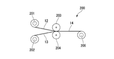
- FIG. 3 is a diagram illustrating a schematic configuration of an example of an annealing apparatus.
- the laminating apparatus 200 shown in FIG. 2 sequentially unwinds the first unwinding film 12 that unwinds the untreated film 12 wound up in a roll shape, and the substrate 13 with an adhesive layer that is wound up in a roll shape.
- a pair of laminating rolls 203 and 204 for laminating the unwinding roll 202, the untreated film 12 and the base material 13 with the adhesive layer to form the laminated body 14; and a winding roll 205 for winding the laminated body 14; Is provided.
- a pair of bonding rolls 203 and 204 bond them by sandwiching and pressing the untreated film 12 and the base material 13 with the adhesive layer between the rolls.
- the base material 13 with the adhesive layer is provided with an adhesive layer on one side of the base material, specifically, the side that comes into contact with the untreated film 12 when the base material passes through the bonding roll 203.
- An annealing apparatus 300 shown in FIG. 3 includes an unwinding roll 301 that sequentially unwinds the laminated body 14 wound up in a roll shape, a heating unit 302 that heats the laminated body 14, a plurality of conveying rolls 303, The laminated body 14, ie, the winding roll 304 which winds up the laminated body 15 of the roll film and the base material 13 with the adhesion layer is provided.
- a space S in which the stacked body 14 is transported is formed in the heating unit 302, and a plurality of transport rolls 303 are arranged in the space S.
- the heating unit 302 is provided with a heating mechanism (not shown) for heating the stacked body 14 introduced into the space S.
- the unwinding roll 301 and the winding roll 304 are used to control the unwinding speed and the unwinding speed of the stacked body 14, and the transport tension and the winding tension applied to the transported stacked body 14 are controlled. It can be controlled.
- the roll film is manufactured by the following procedure. First, in the bonding apparatus 200, the untreated film 12 is conveyed from the 1st unwinding roll 201 to the bonding rolls 203 and 204, and the base material 13 with the adhesive layer is transferred from the 2nd unwinding roll 202 to the bonding roll 203, It conveys to 204, the untreated film 12 and the base material 13 with an adhesion layer are bonded by the bonding rolls 203 and 204, and the obtained laminated body 14 is wound up by the winding roll 205.
- the wound laminate 14 is transferred to the unwinding roll 301 of the annealing apparatus 300, unwound from the unwinding roll 301, conveyed to the heating unit 302, and heated by the heating unit 302 to remove the untreated film 12.
- a roll film is formed, and the laminate 15 of the roll film and the base material 13 with the adhesive layer is wound around a winding roll 304. If necessary, the laminate 15 may be cut into a single sheet. You may peel the base material 13 with the adhesion layer from the laminated body 15 as needed.
- the base material 13 with the adhesive layer is usually peeled off during the production of the copper clad laminate.
- the copper clad laminate using the roll film of the present invention includes a dielectric layer formed by unwinding from the roll film, and a copper layer provided in contact with the dielectric layer.
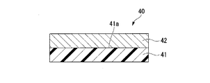
- FIG. 4 is a cross-sectional view schematically showing an example of a copper clad laminate.
- the copper clad laminate 40 shown in FIG. 4 includes a dielectric layer 41 made of an unrolled roll film and a copper layer 42 laminated on the first surface 41a in the thickness direction of the dielectric layer 41.
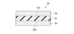
- FIG. 5 is a cross-sectional view schematically showing another example of a copper clad laminate.
- the copper clad laminate 50 shown in FIG. 5 includes a dielectric layer 51 made of an unrolled roll film, and a first copper layer 52 laminated on the first surface 51a in the thickness direction of the dielectric layer 51. And a second copper layer 53 laminated on the second surface 51b opposite to the first surface 51a of the dielectric layer 51.
- the thickness of the copper layer is preferably 3 to 18 ⁇ m. When forming a fine circuit, the thickness of the copper layer is preferably 12 ⁇ m or less.
- the copper layer is preferably formed using a copper foil. Examples of the copper foil include rolled copper foil and electrolytic copper foil.
- the roll film of the present invention (or a product film produced by the production method thereof) is unwound and a copper layer is formed on the surface thereof.
- the copper layer may be formed only on the first surface in the thickness direction of the roll film, or on both the first surface and the second surface opposite to the first surface.
- Examples of the method for forming a copper layer on the surface of the rolled film include a method of laminating (sticking) a copper foil on the surface of the roll film, a vapor deposition method, and a plating method.
- a method of laminating the copper foil a method by hot pressing can be mentioned.
- the hot pressing temperature is preferably from the melting point of the dielectric film + 20 ° C. to the melting point of the dielectric film + 100 ° C.
- the hot pressing time is, for example, 1 to 30 minutes.
- the pressure of the hot press is, for example, 0.1 to 10 MPa.
- the surface treatment includes plasma treatment, corona treatment, ultraviolet (UV) irradiation method, and the like.
- the obtained copper clad laminate can be used as a printed circuit board material.
- the printed circuit board is a plate-shaped component for electrically connecting electronic components such as a semiconductor and a capacitor chip, and at the same time, placing and fixing in a limited space.
- the structure of a well-known printed circuit board is employable.
- the printed circuit board may be a rigid board, a flexible board, or a rigid flexible board.
- the printed circuit board may be a single-sided board, a double-sided board, or a multilayer board (build-up board or the like).
- a copper clad laminate is produced by the copper clad laminate production method, and the copper layer is etched to form a pattern circuit.
- a method for etching the copper layer a known method can be adopted.
- an interlayer insulating film may be formed on the pattern circuit, and a pattern circuit may be further formed on the interlayer insulating film.
- a solder resist may be laminated on the pattern circuit.
- a coverlay film may be laminated.
- the coverlay film is typically composed of a base film and an adhesive layer formed on the surface, and the surface on the adhesive layer side is bonded to the printed circuit board. You may manufacture a buildup board
- the printed circuit board obtained by the printed circuit board manufacturing method of the present invention can be used for various electrical appliances and systems. Above all, it is useful as a board for electronic devices such as radar, network routers, backplanes, wireless infrastructure, etc., various sensor boards for automobiles, and engine management sensors that require high-frequency characteristics. It is suitable for applications intended to reduce loss.
- the contact thickness gauge OG-525H (manufactured by Ono Sokki Co., Ltd.) was used to determine the thickness using a measuring element AA-026 ( ⁇ 10 mm SR7).
- ⁇ Dimensional change rate [%]> A sample obtained by cutting the film into a length (MD) of 12 cm and a width (TD) of 12 cm was prepared and determined by the following method. At 25 ° C., a straight line having a length of about 10 cm is drawn on the sample one by one along the MD and TD directions, and the distance between the end points of each straight line is defined as the initial length L 0 . Next, after heat-treating the sample at 150 ° C. for 30 minutes and cooling to 25 ° C., the linear distance L 1 between the end points of the straight line drawn on the sample is measured, and the dimensional change rate (%) is calculated by the following equation 1. Asked.
- ⁇ Peel test> The produced copper layer laminated body was cut into a width of 1 cm to prepare an evaluation sample.
- the dielectric film and the copper foil were peeled from one end in the length direction of the evaluation sample to a position of 50 mm. Subsequently, it peeled so that it might become 90 degrees at the tensile speed of 100 mm / min using the tensile tester, and the average load of the measurement distance of 20 mm to 80 mm was made into peeling strength (N / cm).
- the room temperature was 25 ° C.
- Each comb pattern 60 includes a plurality of line portions 61 arranged in parallel, and a base portion 62 that extends in a direction orthogonal to the length direction of the line portions 61 and connects the line portions 61.
- a plurality of line portions 61 of one comb pattern 60 and a plurality of line portions 61 of the other comb pattern 60 are alternately arranged in a direction perpendicular to the length direction of the line portion 61,
- the comb patterns 60 are not in contact with each other.
- the length of the line portion 61 was 100 mm
- the width of the line portion 61 was 0.33 mm
- the number of the line portions 61 was 100.
- the interval between adjacent line portions 61 was 0.10 mm.
- a constant temperature and constant temperature of 85 ° C. and 85% RH is obtained using a general-purpose constant temperature and humidity oven (Tabbayespekk PL-1KTH).
- a sample 71 was obtained by holding the treatment time of 500 hours under wet conditions.
- the two comb patterns of the sample 71 are connected to the positive electrode and the negative electrode of the power source 72, respectively, the sample 71 is immersed in the electrolyte L (1 ⁇ mol / L HCl aqueous solution), and a voltage is applied. did.
- the applied current was 20 VDC, and the application time was 100 minutes.
- the sample 71 was taken out from the electrolytic solution L, and the AC resistance value ( ⁇ ⁇ cm) between the two comb patterns was measured under the conditions of 10 Hz and 1 A. From the measured AC resistance value, the stability in the electric corrosion test was determined according to the following criteria. When the two comb patterns come into contact with each other due to deformation or the like, the AC resistance value becomes small. The greater the AC resistance value, the better the stability in the electric corrosion test. ⁇ (Good): AC resistance value exceeds 10 ⁇ 9 ⁇ ⁇ cm. X (defect): AC resistance value is 10 ⁇ 9 ⁇ ⁇ cm or less.
- This PFA has a carboxylic anhydride group as the functional group i.
- the content of carboxylic anhydride groups was 1000 with respect to 1 ⁇ 10 6 carbon atoms in the main chain, the melting temperature was 300 ° C., and the melt flow rate was 17.0 g / 10 minutes.
- PFA2 “P-63P” manufactured by Asahi Glass Co., Ltd., PFA having no functional group i (MFR: 15.0 g / 10 min).
- PFA3 “P-62XP” manufactured by Asahi Glass Co., Ltd., PFA having no functional group i (MFR: 25.0 g / 10 min).
- ETFE1 “C88AX” manufactured by Asahi Glass Co., Ltd., ETFE having no functional group i (MFR: 15 g / 10 min).
- Copper foil “CF-T4X-SVR” manufactured by Fukuda Metal Industry Co., Ltd., electrolytic copper foil, thickness 12 ⁇ m.
- This film is unwound from the unwinding roll 301 using the annealing treatment apparatus 300 having the configuration shown in FIG. 3, transported to the heating unit 302 with a tension of 5 N / m, and 150 ° C. for 5 minutes in the heating unit 302.
- the film was heated under the above conditions and wound on a take-up roll 304 under a tension of 62.5 N / m to obtain a roll film having a thickness of 50 ⁇ m. That is, the annealing treatment conditions were a temperature of 150 ° C., a time of 5 minutes, and a conveyance tension of 5 N / m, and the winding conditions were a winding tension of 62.5 N / m.
- the obtained roll film was unwound and cut into a length of 15 cm and a width of 15 cm, a copper foil of the same size was placed on one surface, and using a vacuum press machine, 340 ° C., 15 minutes, 1.5 MPa
- a copper-clad laminate was obtained by hot pressing under conditions. Table 1 shows the results of the peel test and the electrolytic corrosion test on the obtained copper-clad laminate.
- Example 2 to 14 A roll film was obtained in the same manner as in Example 1 except that the type of fluorine resin, molding conditions, roll-to-roll annealing treatment conditions, and winding conditions were changed as shown in Table 1 to produce a copper clad laminate. The peel test and the electrolytic corrosion test were conducted. The results are summarized in Table 1.
- Example 10 the notation of “PFA1 (10), PFA2 (90)” in Example 10 indicates that PFA1 and PFA2 were used together in this order at a ratio of 10 mass% and 90 mass%.
- Other notations in other examples and tables are the same.
- This film is annealed by the following procedure using the bonding apparatus 200 having the configuration shown in FIG. 2 and the annealing apparatus 300 having the configuration shown in FIG. 3, and the film and the substrate are interposed via the adhesive layer.
- the bonding apparatus 200 the untreated film 12 is conveyed from the 1st unwinding roll 201 to the bonding rolls 203 and 204, and the base material 13 with the adhesive layer is transferred from the 2nd unwinding roll 202 to the bonding roll 203, The untreated film 12 and the base material 13 with the adhesive layer were bonded at room temperature with the bonding rolls 203 and 204, and the obtained laminate 14 was wound around the winding roll 205.
- the base material of the base material 13 with the adhesive layer As the base material of the base material 13 with the adhesive layer, a film having a thickness of 50 ⁇ m obtained by extruding PFA2 pellets in the same manner as described above was used.
- the adhesive layer was formed to a thickness of 2 ⁇ m using a urethane acrylate adhesive.
- the wound laminate 14 is transferred to the unwinding roll 301 of the annealing apparatus 300, unwound from the unwinding roll 301, transported to the heating unit 302 with a tension of 5 N / m, and heated by the heating unit 302. It heated on 150 degreeC and the conditions for 5 minutes, applied the tension
- the obtained roll film was unwound and cut into a length of 15 cm and a width of 15 cm, a copper foil having the same size was placed on the surface on the roll film side (the surface on the PFA 1 side), and the substrate with the adhesive layer was peeled off Then, it heat-pressed on conditions of 340 degreeC, 15 minutes, and 1.5 MPa using the vacuum press machine, and obtained the copper clad laminated body.
- Table 2 shows the results of the peel test and the electrolytic corrosion test on the obtained copper-clad laminate.
- Example 16 to 21 A roll film was obtained in the same manner as in Example 15 except that the type of fluororesin, the base material, and the annealing treatment conditions (temperature, time, transport tension) in the roll-to-roll method were changed as shown in Table 2, and a copper-clad A laminate was manufactured and subjected to a peel test and an electrolytic corrosion test. The results are summarized in Table 2.
- the substrate 13 in Examples 18 and 19 used a PFA2 film having a thickness of 75 ⁇ m instead of a PFA2 film having a thickness of 50 ⁇ m.
- Example 22 A two-layer coextruded film was prepared by the following procedure.
- PFA1 is melted at a set temperature of 340 ° C. using a 15 mm ⁇ single screw extruder (manufactured by Tanabe Plastic Machinery Co., Ltd.) and supplied to the first manifold of a 400 m wide two-layer multi-manifold die.
- ETFE1 was supplied by being melted at a set temperature of 340 ° C. using a 30 mm ⁇ single screw extruder (manufactured by Ikegai Co., Ltd.), and each molten resin was extruded from the multi-manifold die into a film at a molding speed of 2 m / min.
- a coextruded film having a thickness of the first layer (PFA1) of 25 ⁇ m, a thickness of the second layer (ETFE1) of 75 ⁇ m, and a width of 320 mm was obtained.
- This coextruded film was annealed in the same manner as in Example 1 to obtain a take-up roll film.
- the change rate MD of this roll film was 0.03, and the change rate TD was 0.02.
- the peel strength of the copper clad laminate obtained using this roll film was 8.4 N / m, the AC resistance value was 8.4 ⁇ 10 ⁇ 9 ⁇ ⁇ cm, and the determination was “ ⁇ ”.
Landscapes
- Chemical & Material Sciences (AREA)
- Engineering & Computer Science (AREA)
- Manufacturing & Machinery (AREA)
- Polymers & Plastics (AREA)
- Chemical Kinetics & Catalysis (AREA)
- Organic Chemistry (AREA)
- Medicinal Chemistry (AREA)
- Health & Medical Sciences (AREA)
- Materials Engineering (AREA)
- Microelectronics & Electronic Packaging (AREA)
- Physics & Mathematics (AREA)
- Thermal Sciences (AREA)
- General Chemical & Material Sciences (AREA)
- Spectroscopy & Molecular Physics (AREA)
- Laminated Bodies (AREA)
- Manufacture Of Macromolecular Shaped Articles (AREA)
- Storage Of Web-Like Or Filamentary Materials (AREA)
- Controlling Rewinding, Feeding, Winding, Or Abnormalities Of Webs (AREA)
- Treatments Of Macromolecular Shaped Articles (AREA)
- Processing And Handling Of Plastics And Other Materials For Molding In General (AREA)
- Extrusion Moulding Of Plastics Or The Like (AREA)
Abstract
Description
両面基板や多層基板の製造においては、層間接続のためにスルーホールめっきが多用されている。スルーホールめっきでは、一般に、パネルめっきと呼ばれる全面めっきで層間接続用の穴内と基板表面を銅めっき膜で被覆する。回路パターンは、銅箔とその上に形成された銅めっき膜を一括エッチングすることで形成される。最近の微細回路基板では、エッチング精度向上のため、厚さ12μm以下の薄銅箔が多用される。中でもライン幅50μm、スペース幅50μm程度のラインアンドスペースパターンのような微細回路の形成では、厚さ5μmの極薄めっき銅箔を用いることで、回路形成時の銅厚を低減し、エッチング精度向上を容易にしている。
スルーホールめっきされたプリント基板には、仕上り状態の評価及び信頼性試験が行われる。仕上り状態の評価は、めっき厚、めっき形状、めっき物性の3項目である。信頼性試験は、温度サイクルによる疲労寿命評価と、電食試験と呼ばれる恒温恒湿バイアス下での絶縁寿命評価が中心となる。電食試験では、くし型パターンを用いたパターン間絶縁信頼性試験が重要な信頼性試験であることが知られている(非特許文献1)。
フッ素樹脂フィルムは、誘電特性に優れることが知られている。しかし、そのロールフィルムを用いて製造されるプリント基板は電食試験での安定性が未だ充分ではない点と、その原因がロールフィルムの寸法安定性に起因する点とを、本発明者らは知見している。そのため、フッ素樹脂のロールフィルムを使用して、電食試験で優れた安定性を示すプリント基板を効率よく製造するのが困難である。
本発明の目的は、電食試験での安定性に優れたプリント基板の効率的な製造に適する、フッ素樹脂のロールフィルム及びその製造方法と、前記ロールフィルムを用いた、銅張積層体及びプリント基板の製造方法との提供である。
[1] 25℃における寸法を基準として150℃で30分間加熱し、その後25℃まで冷却した際のMD及びTD各々の寸法変化率の絶対値が1.0%未満である、熱溶融性フッ素樹脂を主成分とする、厚さが1~100μmのロールフィルム。
[2] 前記MDの寸法変化率の絶対値に対する巻き取りにおける張力の比が、100~1000000である、[1]に記載のロールフィルム。
[3] 銅張樹脂積層体に用いられる、[1]又は[2]に記載のロールフィルム。
[4] 前記熱溶融性フッ素樹脂が、テトラフルオロエチレンに由来する単位とペルフルオロ(アルキルビニルエーテル)に由来する単位とを含むフッ素樹脂である、[1]~[3]のいずれか1項に記載のロールフィルム。
[5] 前記熱溶融性フッ素樹脂が、イオン捕捉能を発揮する官能基を有するフッ素樹脂である、[1]~[4]のいずれか1項に記載のロールフィルム。
[6] イオン捕捉能を発揮する官能基を有する熱溶融性フッ素樹脂と該熱溶融性フッ素樹脂以外の熱溶融性フッ素樹脂とを主成分とする、[1]~[5]のいずれか1項に記載のロールフィルム。
[7] 熱溶融性フッ素樹脂の層とイオン捕捉能を発揮する官能基を有する熱溶融性フッ素樹脂の層とを有する、[1]~[6]のいずれか1項に記載のロールフィルム。
[8] イオン捕捉能を発揮する官能基が、カルボニル基、カルボキシ基、カルボン酸無水物基(-C(=O)-O-C(=O)-)、カルボン酸エステル基、スルフォニル基、スルホ基及びスルフォン酸無水物基(-S(=O)2-O-S(=O)2-)からなる群から選ばれる少なくとも1種である、[5]~[7]のいずれか1項に記載のロールフィルム。
[9] 厚さが、3~75μmである、[1]~[8]のいずれか1項に記載のロールフィルム。
[10] [1]~[9]のいずれか1項に記載のロールフィルムの製造方法であって、熱溶融性フッ素樹脂を主成分とする厚さが1~100μmのフィルムを、前記熱溶融性フッ素樹脂の溶融温度(Tm)より210℃低い温度からTmから20℃低い温度にてアニール処理してから巻き取る、方法。
[11] 前記フィルムにかかる張力を10N/m以下として前記アニール処理をする、[10]に記載の製造方法。
[12] 前記フィルムにかかる張力を500N/m以下として前記フィルムを巻き取る、[10]又は[11]に記載の製造方法。
[13] [1]~[9]のいずれか1項に記載のロールフィルムを巻き出し、巻き出されたフィルムの表面に銅層を形成する、銅張積層体の製造方法。
[14] 交流抵抗値が1.0×10⁻⁹Ω・cm超の銅層を形成する、[13]に記載の製造方法。
[15] [13]又は[14]に記載の製造方法により銅張積層体を製造し、前記銅層をエッチングしてパターン回路を形成する、プリント基板の製造方法。
「MD」は、流れ方向(Machine Direction)を意味し、「TD」は、MDと直交する方向(Transverse Direction)を意味する。
「寸法変化率」は、25℃における寸法を基準として150℃で30分間加熱し、その後25℃まで冷却した際の寸法の変化率であり、詳しくは後述する実施例に記載の方法により求められる。
「熱溶融性樹脂」とは、溶融流動性の樹脂を意味し、荷重49Nの条件下、樹脂の融点よりも20℃以上高い温度において、溶融流れ速度が0.1~1000g/10分となる温度が存在する樹脂を意味する。
「溶融流れ速度」とは、JIS K 7210:1999(ISO 1133:1997)に規定される、樹脂のメルトマスフローレート(MFR)を意味する。
「溶融温度」とは、示差走査熱量測定(DSC)法で測定した、樹脂の融解ピークの最大値に対応する温度を意味する。
「ガラス転移温度」(以下、Tgとも記す。)とは、樹脂のアモルファス領域の分子状態に起因する転移温度の一つで、Tgより低い温度では樹脂の主鎖の凍結が生じ、ガラス状態を示すようになる。Tgは、フィルムの固体動的粘弾性測定(DMA)法で測定したtanδピークの最大値を示す温度に対応する温度を意味する。
樹脂(重合体)における「単位」とは、単量体の重合により形成された前記単量体に由来する原子団を意味する。単位は、重合反応によって直接形成された単位であってもよく、重合体を処理することによって前記単位の一部が別の構造に変換された単位であってもよい。以下、単量体に由来する単位を、単に「単量体の単位」とも記す。
数値範囲を示す「~」は、その前後に記載された数値を下限値及び上限値として含むことを意味する。
図1~図7における寸法比は、説明の便宜上、実際のものとは異なったものである。
フッ素樹脂の溶融温度は、260~320℃が好ましく、280~310℃が特に好ましい。
フッ素樹脂のMFRは、荷重49Nの条件下、フッ素樹脂の溶融温度よりも20℃以上高い温度において、0.1~100g/10分が好ましく、1~40g/10分がより好ましく、5~30g/10分が特に好ましい。この場合、フッ素樹脂の成形加工性とロールフィルムの機械強度とがバランスしやすい。
フッ素樹脂の比誘電率は、例えば、フッ素樹脂に含まれるフルオロオレフィンの単位の種類や含有量により調整できる。
官能基iとは、80℃以上300℃以下の温度でアニール処理を行ったときにイオン性物質を捕捉する作用を有する官能基である。電食現象は、腐食現象が大きな要因と考えられる。腐食現象は、回路を形成する材料の電気化学的な反応又は変質により発生したイオンや、外部から表面付着等により取り込まれたイオン性物質(大気中の塩化水素、NOx,SOx等を吸着した粉塵や、油分等の付着物や、はんだフラックス、絶縁接着層等の他の基板構成材料に含まれる各種添加剤に由来するカウンターカチオン類。)が、マイグレーションや電気的な力によって移動し、電極作用をもつ物質表面にて電気化学的に反応して生じる。官能基iは、電食を引き起こす原因となりうるイオン性物質と反応し、不要なイオン性物質を固定化又は無害化すると考えられる。
官能基iを有する単量体としては、後述するカルボン酸無水物基を含む環状単量体、ペルフルオロ[2-(フルオロスルホニルエトキシ)プロピルビニルエーテル]、メチルペルフルオロ-5-オキシ-6-ヘプテノエート(以下、「MXM」とも記す。)等が挙げられる。
フッ素樹脂iは、含フッ素量と加工性を両立する観点から、官能基iを有するPFA、官能基iを有するFEP、TFE/MXM重合体が好ましい。
前記環状単量体は、IAH、CAH及びNAHが好ましく、前記密着性にさらに優れる観点から、IAH及びNAHが好ましい。
PAVEとしては、CF2=CFOCF2CF3、CF2=CFOCF2CF2CF3(PPVE)、CF2=CFOCF2CF2CF2CF3、CF2=CFO(CF2)8Fが挙げられ、PPVEが好ましい。
単位u1の割合は、90~99.89モル%が好ましく、95~99.47モル%がより好ましく、96~98.95モル%がさらに好ましい。
単位u2の割合は、0.01~3モル%が好ましく、0.03~2モル%がより好ましく、0.05~1モル%がさらに好ましい。この場合、フッ素樹脂iiにおける、巻き出したロールフィルムと銅層との界面における密着性にさらに優れる。
単位u3の割合は、0.1~9.99モル%が好ましく、0.5~9.97モル%がより好ましく、1~9.95モル%がさらに好ましい。この場合、フッ素樹脂iiの成形性、ロールフィルムの耐屈曲性等にさらに優れる。
他の単量体としては、オレフィン(エチレン、プロピレン、1-ブテン等)、ビニルエステル(酢酸ビニル等)等が挙げられる。他の単量体は、1種を単独で用いてもよく、2種以上を併用してもよい。この他の単量体としては、ロールフィルムの機械的強度等の観点から、エチレン、プロピレン、1-ブテンが好ましく、エチレンが特に好ましい。
他の樹脂としては、非熱溶融性フッ素樹脂、含フッ素エラストマー、フッ素原子を含まない樹脂等が挙げられる。
無機フィラーとしては、シリカ、中空シリカ、クレー、タルク、炭酸カルシウム、マイカ、珪藻土、アルミナ、酸化亜鉛、酸化チタン、酸化カルシウム、酸化マグネシウム、酸化鉄、酸化錫、酸化アンチモン、水酸化カルシウム、水酸化マグネシウム、水酸化アルミニウム、塩基性炭酸マグネシウム、炭酸マグネシウム、炭酸亜鉛、炭酸バリウム、ドーソナイト、ハイドロタルサイト、硫酸カルシウム、硫酸バリウム、珪酸カルシウム、モンモリロナイト、ベントナイト、活性白土、セピオライト、イモゴライト、セリサイト、ガラス繊維、ガラスビーズ、シリカ系バルーン、カーボンブラック、カーボンナノチューブ、カーボンナノホーン、グラファイト、炭素繊維、ガラスバルーン、炭素バルーン、木粉、ホウ酸亜鉛等が挙げられる。無機フィラーは、多孔質であってもよく、非多孔質であってもよい。無機フィラーは、樹脂への分散性の向上の点から、シランカップリング剤、チタネートカップリング剤等の表面処理剤による表面処理が施されてもよい。無機フィラーは、1種を単独で用いてもよく、2種以上を併用してもよい。
有機フィラーとしては、他の樹脂を主成分とする粒子フィラー、特に低誘電特性を有する材料からなる粒子フィラーが好ましく、PTFE、ポリスチレン又はポリオレフィンの粒子フィラーや、それらの樹脂の中空フィラー等が挙げられる。
前記態様において、フッ素樹脂iはフッ素樹脂iiが好ましく、フッ素樹脂i以外のフッ素樹脂は官能基iを有さないPFAが好ましい。
前記態様における、ロールフィルムのフッ素樹脂の全量に占める、フッ素樹脂iの割合は、0.1~49質量%が好ましく、5~40質量%がより好ましい。フッ素樹脂i以外のフッ素樹脂の割合は、51~99.9質量%が好ましく、60~95質量%がより好ましい。
ロールフィルムは、フッ素樹脂のフィルムのみからなっていてもよく、他の基材の表面に形成されていてもよい。前者の場合、1層のフッ素樹脂のフィルムからなっていてもよく、2層以上のフッ素樹脂のフィルムからなっていてもよい。後者の場合、他の基材として、フッ素樹脂のフィルムを使用してもよい。
通常の熱溶融性フッ素樹脂のロールフィルムは、その製法(押出成形による溶融成形法等)に起因する成形歪が残存する。そのため、そのロールフィルムの寸法変化率は1.0%を超える。そこで、本発明は、フッ素樹脂のフィルムの厚さと、後述する、アニール処理の条件やフィルムの巻取条件の調整とにより、ロールフィルムのMD及びTD各々の寸法変化率を所定の範囲に収束させつつ、電食現象を抑制している。そのため、本発明のロールフィルムを巻き出して銅層を形成すれば高精度な銅張積層体が得られ、電食現象が抑制されたプリント基板が得られる。
変化率TDは、0.5%未満が好ましく、0.1%以下が好ましく、0.08%以下がより好ましく、0.05%以下が特に好ましい。
さらに、変化率TDに対する変化率MDの比は、5以下が好ましく、3以下が特に好ましい。この場合、ロールフィルムが長尺であっても、より高精度なプリント基板を製造できる。前記比の下限は、通常、1である。
また、フッ素樹脂が官能基iを有すれば、ロールフィルムと銅層の密着性も高まる。
フッ素樹脂が官能基iを有すれば、イオン性物質が官能基iによってイオン性物質が固定化又は無害化されているため、電食試験での安定性により優れたプリント基板が得られる。また、官能基iがフッ素樹脂の主鎖に化学的に結合しているため、フッ素樹脂中に官能基iを含む低分子材料を含む場合に比べて、フィルム内での官能基iのモビリティが低い。そのため、回路通電時に生じる電場、磁場等によるイオン電導、拡散等を抑制でき、イオン性物質の固定化又は無害化効果が大きいと考えられる。
未処理フィルムは、変化率MDと変化率TDは各々1.0%超であり、典型的には、各々1.0%超5%以下である。
アニール処理においては、フィルムのMDに対して、張力をかけるのが好ましい。この際の張力は、10N/m以下が好ましく、5N/m以下が特に好ましい。この際の張力の下限は、通常、1N/mである。
アニール処理したフィルムの巻き取りにおいては、フィルムのMDに対して、張力(以下、「巻取張力」とも記す。)をかけるのが好ましい。巻取張力は、500N/m以下が好ましく、300N/m以下がより好ましく、150N/m以下が特に好ましい。この際の張力の下限は、通常、1N/mである。また、巻取張力は、変化率MDの絶対値に対する比が、100~1000000になるのが好ましく、300~10000になるのが特に好ましい。
図1は、未処理フィルムの製造装置100の一例を模式的に示す図である。
製造装置100は、押出機101と、押出機101に取り付けられたTダイ102と、急冷ロール103と、複数の冷却ロール104と、一対のニップロール105と、巻取ロール106とを備える。
複数の冷却ロール104は、Tダイ102から吐出されたフィルム状の溶融体11が、一対のニップロール105側に向かって複数の冷却ロール104を順次通過するように直列に配置されている。なお、ここでは3つの冷却ロール104を示したが、冷却ロール104の数は3つに限定されず、1つでもよい。
急冷ロール103は、複数の冷却ロール104のうち最もTダイ102に近い冷却ロール104(以下、「第1の冷却ロール」とも記す。)に対向配置されている。
押出機101によって、フッ素樹脂を含み、必要に応じて、フッ素樹脂以外の他の樹脂、添加剤等を含む材料を溶融し、押出機101から押し出された溶融樹脂をTダイ102に供給し、Tダイ102から溶融樹脂をフィルム状に吐出し、フィルム状の溶融体11を、急冷ロール103によって第1の冷却ロール104に押し付け、次いで残りの冷却ロール104に順次接触させて冷却し、一対のニップロール105の間を通過させて搬送し、未処理フィルム12とする。得られた未処理フィルム12は、巻取ロール106に巻き取る。必要に応じて、未処理フィルム12を裁断して枚葉状としてもよい。
成形速度、すなわちTダイ102からの溶融体11の吐出速度は、1~100m/分が好ましく、1~30m/分が特に好ましい。成形速度が前記範囲内であると、フィルム平坦性が優れる。成形速度が前記範囲の下限値未満であると、溶融体11が冷却ロールに接触する前に冷却されるので、フィルム平坦性が悪くなるおそれがある。成形速度が前記範囲の上限値超であると、フィルム冷却が遅れるので、フィルム平坦性が悪くなるおそれがある。
溶融体11がTダイ102から吐出されてから第1の冷却ロール104に接触点までの距離は、500mm以下が好ましく、300mm以下が特に好ましい。前記時間の下限は、例えば100mmである。
冷却ロール104の表面温度は、樹脂材料中のTm未満であり、室温以上かつ(Tm-20℃)以下が好ましい。
急冷ロール103の表面温度は、冷却ロール104の表面温度と同様であってよい。
未処理フィルムをロールツーロールでMDに搬送しながら加熱する場合、搬送時に未処理フィルムにかかる張力(以下、「搬送張力」とも記す。)は、アニール処理として加熱されている領域で1N/m以上が好ましい。搬送張力が前記下限値以上であると、フィルムを安定的に搬送できる。
樹脂フィルムを構成する樹脂としては、熱溶融性フッ素樹脂、非熱溶融性フッ素樹脂、非フッ素系樹脂等が挙げられる。非フッ素系樹脂としては、ポリエステル樹脂(ポリエチレンテレフタレート(PET)樹脂、ポリエチレンナフタレート樹脂(PEN)等)、ポリイミド樹脂等が挙げられる。
樹脂フィルムとしては、他の基材と未処理フィルムの線膨張係数が近く、アニール処理時にカールが発生しにくい点から、フッ素樹脂のフィルムが好ましい。フッ素樹脂のフィルムを構成するフッ素樹脂は、基材と未処理フィルムの線膨張係数がより近く、アニール処理時にカールがより発生しにくい点から、未処理フィルムに含まれるフッ素樹脂と同種のフッ素樹脂が好ましい。例えば、フッ素樹脂がPFAである場合、樹脂フィルムを構成する樹脂もPFAであることが好ましい。樹脂フィルムを構成するフッ素樹脂は、官能基iを有していなくてもよい。
基材の厚さは、25~100μmが好ましい。
基材と未処理フィルムとが直接積層された積層体は、例えば、前記製造方法において、熱溶融性フッ素樹脂を含む樹脂材料とともに、基材フィルムを構成する樹脂材料を共押し出しする方法により得られる。共押し出しの手法としては、フィードブロック法、マルチマニホールド法等が挙げられる。
基材と未処理フィルムとを粘着層を介して積層する場合、粘着層を構成する粘着剤は、特に限定されず、アクリル系、シリコーン系、ウレタン系、ポリオレフィン系等が挙げられる。
粘着層の厚さは、0.1~5μmが好ましく、0.5~2μmが特に好ましい。
一対の貼合ロール203,204は、それらのロール間に未処理フィルム12と粘着層付き基材13とを挟持して加圧することで、それらを貼合する。
粘着層付き基材13は、基材の片面、具体的には基材が貼合ロール203を通過する際に未処理フィルム12と接する側の面に粘着層が設けられたものである。
加熱部302には、積層体14が搬送な空間Sが形成されており、空間S内に複数の搬送ロール303が配置されている。また、加熱部302には、空間Sに導入された積層体14を加熱するための加熱機構(図示せず)が設けられている。
アニール処理装置300においては、巻出ロール301及び巻取ロール304により、積層体14の巻き出し速度及び巻き取り速度を制御して、搬送される積層体14にかかる搬送張力と巻取張力とを制御できるようになっている。
まず、貼合装置200にて、未処理フィルム12を第1巻出ロール201から貼合ロール203,204に搬送し、粘着層付き基材13を第2巻出ロール202から貼合ロール203,204に搬送し、貼合ロール203,204にて未処理フィルム12と粘着層付き基材13とを貼合し、得られた積層体14を巻取ロール205に巻き取る。
次に、巻き取った積層体14をアニール処理装置300の巻出ロール301に移し、巻出ロール301から巻き出して加熱部302に搬送し、加熱部302にて加熱して未処理フィルム12をロールフィルムとし、ロールフィルムと粘着層付き基材13との積層体15を巻取ロール304に巻き取る。必要に応じて、積層体15を裁断して枚葉状としてもよい。必要に応じて、積層体15から粘着層付き基材13を剥離してもよい。粘着層付き基材13は通常、銅張積層体の製造時に剥離される。
図5は、銅張積層体の他の一例を模式的に示す断面図である。図5に示す銅張積層体50は、巻き出されたロールフィルムからなる誘電体層51と、誘電体層51の厚さ方向の第1の表面51aに積層された第1の銅層52と、誘電体層51の第1の表面51aとは反対側の第2の表面51bに積層された第2の銅層53と、を備える。
銅層は、銅箔を用いて形成することが好ましい。銅箔としては、圧延銅箔、電解銅箔等が挙げられる。
銅層を形成するのは、ロールフィルムの厚さ方向の第1の表面のみでもよく、第1の表面及び第1の表面とは反対側の第2の表面の両方でもよい。
銅箔を積層する方法としては、熱プレスによる方法が挙げられる。熱プレスの温度は、誘電体フィルムの融点+20℃~誘電体フィルムの融点+100℃が好ましい。熱プレスの時間は、例えば1~30分間である。熱プレスの圧力は、例えば0.1~10MPaである。
プリント基板は、半導体やコンデンサチップ等の電子部品を電気的に接続すると同時に、限られた空間内に配置し固定するための板状部品である。
本銅張積層体から形成されるプリント基板の構成に特に制限はなく、公知のプリント基板の構成を採用できる。プリント基板は、リジッド基板、フレキシブル基板、リジッドフレキシブル基板のいずれであってもよい。プリント基板は、片面基板、両面基板、多層基板(ビルドアップ基板等)のいずれであってもよい。
銅層のエッチング方法としては、公知の方法を採用できる。
プリント基板の製造では、前記パターン回路上にソルダーレジストを積層してもよい。
プリント基板の製造では、カバーレイフィルムを積層してもよい。カバーレイフィルムは、典型的には、基材フィルムと、その表面に形成された接着剤層とから構成され、接着剤層側の面がプリント基板に貼り合わされる。
銅張積層体の銅層をエッチングして得られた基板を内層回路基板としてビルドアップ基板を製造してもよい。
各例で使用した測定又は試験方法、及び材料を以下に示す。
<MFR[g/10分]>
メルトインデクサー(テクノ・セブン社製)を用い、372℃、49N荷重下で、直径2mm、長さ8mmのノズルから10分間に流出するフッ素樹脂の質量(g)を測定して求めた。
接触式厚み計OG-525H(小野測器社製)にて、測定子AA-026(φ10mm SR7)を使用して求めた。
フィルムを長さ(MD)12cm×幅(TD)12cmに裁断した試料を調製し、下記の方法で求めた。
25℃において、試料に約10cmの長さの直線を、MD及びTDそれぞれの方向に沿って1本ずつ描き、各直線の端点間距離を初期長L0とする。次いで、前記試料を150℃で30分間熱処理し、25℃まで冷却した後、試料上に描かれた直線の端点間の直線距離L1を測定し、下式1により寸法変化率(%)を求めた。
寸法変化率(%)=(L1/L0-1)×100 ・・・式1
MDに沿った直線について求めた寸法変化率の絶対値をMDの寸法変化率(変化率MD)とし、TDに沿った直線について求めた寸法変化率の絶対値をTDの寸法変化率(変化率TD)とした。
作製した銅層積層体を幅1cmにカットし、評価サンプルを作成した。評価サンプルの長さ方向の一端から50mmの位置まで誘電体フィルムと銅箔との間を剥離した。ついで、引張試験機を用いて、室温下、引張速度100mm/分で90°となるように剥離し、測定距離20mmから80mmの平均荷重を剥離強度(N/cm)とした。室温は25℃であった。
“ガラス基材銅張積層板の絶縁信頼性”,サーキットテクノロジ Vol.3,No.4,p212-219(1988)に記載された簡易電食性評価法に従った。
電食試験では、図6に示す、2つのくし形パターン60が組み合わされたパターンを用いる。各くし形パターン60は、平行に配置された複数のライン部61と、それらのライン部61の長さ方向と直交する方向に延び、各ライン部61を接続する基部62とからなる。前記パターンにおいては、一方のくし形パターン60の複数のライン部61と他方のくし形パターン60の複数のライン部61とが、ライン部61の長さ方向と直交する方向に交互に配置され、かつ各くし型パターン60同士が接触していない。各くし形パターン60において、ライン部61の長さは100mm、ライン部61の幅は0.33mm、ライン部61の本数は100本とした。隣り合うライン部61間の間隔は0.10mmとした。
図7に示すように、試料71の2つのくし形パターンをそれぞれ電源72の+極、-極に接続し、試料71を電解液L(1μmol/LのHCl水溶液)に浸漬し、電圧を印加した。印加電流は20VDC、印加時間は100分とした。その後、試料71を電解液Lから取り出し、10Hz、1Aの条件で、2つのくし形パターン間の交流抵抗値(Ω・cm)を測定した。
測定された交流抵抗値から、電食試験での安定性を以下の基準で判定した。2つのくし形パターンが変形する等により相互に接触すると、交流抵抗値が小さくなる。交流抵抗値が大きいほど、電食試験での安定性に優れる。
〇(良好):交流抵抗値が10-9Ω・cm超。
×(不良):交流抵抗値が10-9Ω・cm以下。
PFA1:国際公開第2016/017801号の[0124]と同様に合成して得たPFA。各単位の割合はTFE/NAH/PPVE=97.9/0.1/2.0モル%である。このPFAは官能基iとしてカルボン酸無水物基を有する。カルボン酸無水物基の含有量は主鎖炭素数1×106個に対し1000個であり、溶融温度は300℃であり、溶融流れ速度は17.0g/10分であった。
PFA2:旭硝子社製「P-63P」、官能基iを有しないPFA(MFR:15.0g/10分)。
PFA3:旭硝子社製「P-62XP」、官能基iを有しないPFA(MFR:25.0g/10分)。
ETFE1:旭硝子社製「C88AX」、官能基iを有しないETFE(MFR:15g/10分)。
銅箔:福田金属工業社製「CF-T4X-SVR」、電解銅箔、厚さ12μm。
PFA1のペレットを、700mm幅のTダイを有する65mmφ単軸押出機(東芝機械社製、L/D=25、圧縮比3.1)を用い、成形温度340℃、成形速度3.5m/分でフィルム状に押出成形し、厚さ50μm、幅510mmのフィルム(ロール状に巻き取られた未処理フィルム)を得た。
得られたロールフィルムを巻き出して、長さ15cm×幅15cmにカットし、一方の表面に同じ大きさの銅箔を配置し、真空プレス機を用い、340℃、15分、1.5MPaの条件で熱プレスして銅張積層体を得た。
得られた銅張積層体について、剥離試験及び電食試験をした結果を、表1に示す。
フッ素樹脂の種類、成形条件、ロールtoロール方式でのアニール処理条件、巻取条件を表1に示すように変更した以外は例1と同様にしてロールフィルムを得て、銅張積層体を製造し、その剥離試験及び電食試験をした。結果をまとめて、表1に示す。

PFA1を、1900mm幅のTダイを有する65mmφ単軸押出機(東芝機械社製、L/D=25、圧縮比3.1)を用い、成形温度340℃、成形速度20m/分でフィルム状に押出成形し、厚さ25μm、幅1500mmのフィルムを得た。
まず、貼合装置200にて、未処理フィルム12を第1巻出ロール201から貼合ロール203,204に搬送し、粘着層付き基材13を第2巻出ロール202から貼合ロール203,204に搬送し、貼合ロール203,204にて、室温で、未処理フィルム12と粘着層付き基材13とを貼合し、得られた積層体14を巻取ロール205に巻き取った。
粘着層付き基材13の基材としては、PFA2のペレットを前記と同様に押出成形して得た厚さ50μmのフィルムを用いた。粘着層は、ウレタンアクリレート系粘着剤を用いて厚さ2μmに形成した。
次に、巻き取った積層体14をアニール処理装置300の巻出ロール301に移し、巻出ロール301から巻き出し、5N/mの張力をかけて加熱部302に搬送し、加熱部302にて150℃、5分の条件で加熱し、100N/m以下の張力をかけて巻取ロール304に巻き取ってロールフィルムを得た。つまり、アニール処理条件は温度150℃、時間5分、搬送張力5N/mとし、巻き取り条件は巻取張力100N/m以下とした。
得られた銅張積層体について、剥離試験及び電食試験をした結果を、表2に示す。
フッ素樹脂の種類、基材およびロールtoロール方式でのアニール処理条件(温度、時間、搬送張力)を表2に示すように変更した以外は例15と同様にしてロールフィルムを得て、銅張積層体を製造し、その剥離試験及び電食試験をした。結果をまとめて、表2に示す。

以下の手順で、2層構造の共押出フィルムを作成した。400m幅2層マルチマニホールドダイの第1のマニホールドに、PFA1を、15mmφ単軸押出機(田辺プラスチック機械社製)を用い、設定温度340℃にて溶融させて供給し、第2のマニホールドに、ETFE1を、30mmφ単軸押出機(池貝社製)を用い、設定温度340℃にて溶融させて供給し、各溶融樹脂を前記マルチマニホールドダイから成形速度2m/分でフィルム状に押出成形し、第1の層(PFA1)の厚さが25μm、第2の層(ETFE1)の厚さが75μm、幅320mmの共押出フィルムを得た。この共押出フィルムを例1と同様にして、アニール処理して巻き取りロールフィルムを得た。このロールフィルムの変化率MDは0.03であり、変化率TDは0.02であった。このロールフィルムを用いて得られる銅張積層体の剥離強度は8.4N/mであり、交流抵抗値は8.4×10-9Ω・cmであり、判定は「○」であった。
なお、2018年04月20日に出願された日本特許出願2018-081794号の明細書、特許請求の範囲、要約書及び図面の全内容をここに引用し、本発明の明細書の開示として、取り入れるものである。
Claims (15)
- 25℃における寸法を基準として150℃で30分間加熱し、その後25℃まで冷却した際のMD及びTD各々の寸法変化率の絶対値が1.0%未満である、熱溶融性フッ素樹脂を主成分とする、厚さが1~100μmのロールフィルム。
- 前記MDの寸法変化率の絶対値に対する巻き取りにおける張力の比が、100~1000000である、請求項1に記載のロールフィルム。
- 銅張樹脂積層体に用いられる、請求項1又は2に記載のロールフィルム。
- 前記熱溶融性フッ素樹脂が、テトラフルオロエチレンに由来する単位とペルフルオロ(アルキルビニルエーテル)に由来する単位とを含むフッ素樹脂である、請求項1~3のいずれか1項に記載のロールフィルム。
- 前記熱溶融性フッ素樹脂が、イオン捕捉能を発揮する官能基を有するフッ素樹脂である、請求項1~4のいずれか1項に記載のロールフィルム。
- イオン捕捉能を発揮する官能基を有する熱溶融性フッ素樹脂と該熱溶融性フッ素樹脂以外の熱溶融性フッ素樹脂とを主成分とする、請求項1~5のいずれか1項に記載のロールフィルム。
- 熱溶融性フッ素樹脂の層とイオン捕捉能を発揮する官能基を有する熱溶融性フッ素樹脂の層とを有する、請求項1~6のいずれか1項に記載のロールフィルム。
- イオン捕捉能を発揮する官能基が、カルボニル基、カルボキシ基、カルボン酸無水物基(-C(=O)-O-C(=O)-)、カルボン酸エステル基、スルフォニル基、スルホ基及びスルフォン酸無水物基(-S(=O)2-O-S(=O)2-)からなる群から選ばれる少なくとも1種である、請求項5~7のいずれか1項に記載のロールフィルム。
- 厚さが、3~75μmである、請求項1~8のいずれか1項に記載のロールフィルム。
- 請求項1~9のいずれか1項に記載のロールフィルムの製造方法であって、
熱溶融性フッ素樹脂を主成分とする厚さが1~100μmのフィルムを、前記熱溶融性フッ素樹脂の溶融温度(Tm)より210℃低い温度からTmから20℃低い温度にてアニール処理してから巻き取る、方法。 - 前記フィルムにかかる張力を10N/m以下として前記アニール処理をする、請求項10に記載の製造方法。
- 前記フィルムにかかる張力を500N/m以下として前記フィルムを巻き取る、請求項10又は11に記載の製造方法。
- 請求項1~9のいずれか1項に記載のロールフィルムを巻き出し、巻き出されたフィルムの表面に銅層を形成する、銅張積層体の製造方法。
- 交流抵抗値が1.0×10⁻⁹Ω・cm超の銅層を形成する、請求項13に記載の製造方法。
- 請求項13又は14に記載の製造方法により銅張積層体を製造し、前記銅層をエッチングしてパターン回路を形成する、プリント基板の製造方法。
Priority Applications (6)
| Application Number | Priority Date | Filing Date | Title |
|---|---|---|---|
| CN201980026793.5A CN111989358B (zh) | 2018-04-20 | 2019-04-16 | 卷膜、卷膜的制造方法、覆铜层叠体的制造方法、以及印刷基板的制造方法 |
| KR1020207022979A KR20210003084A (ko) | 2018-04-20 | 2019-04-16 | 롤 필름, 롤 필름의 제조 방법, 구리 피복 적층체의 제조 방법, 및 프린트 기판의 제조 방법 |
| JP2020514404A JP7338619B2 (ja) | 2018-04-20 | 2019-04-16 | ロールフィルム、ロールフィルムの製造方法、銅張積層体の製造方法、及びプリント基板の製造方法 |
| US17/021,054 US20200407524A1 (en) | 2018-04-20 | 2020-09-15 | Roll film, method for producing roll film, method for producing copper-clad laminate and method for producing printed board |
| JP2023135905A JP2023164464A (ja) | 2018-04-20 | 2023-08-23 | ロールフィルム、ロールフィルムの製造方法、銅張積層体の製造方法、及びプリント基板の製造方法 |
| US18/588,831 US12466927B2 (en) | 2018-04-20 | 2024-02-27 | Roll film, method for producing roll film, method for producing copper-clad laminate and method for producing printed board |
Applications Claiming Priority (2)
| Application Number | Priority Date | Filing Date | Title |
|---|---|---|---|
| JP2018081794 | 2018-04-20 | ||
| JP2018-081794 | 2018-04-20 |
Related Child Applications (1)
| Application Number | Title | Priority Date | Filing Date |
|---|---|---|---|
| US17/021,054 Continuation US20200407524A1 (en) | 2018-04-20 | 2020-09-15 | Roll film, method for producing roll film, method for producing copper-clad laminate and method for producing printed board |
Publications (1)
| Publication Number | Publication Date |
|---|---|
| WO2019203243A1 true WO2019203243A1 (ja) | 2019-10-24 |
Family
ID=68240341
Family Applications (1)
| Application Number | Title | Priority Date | Filing Date |
|---|---|---|---|
| PCT/JP2019/016355 Ceased WO2019203243A1 (ja) | 2018-04-20 | 2019-04-16 | ロールフィルム、ロールフィルムの製造方法、銅張積層体の製造方法、及びプリント基板の製造方法 |
Country Status (6)
| Country | Link |
|---|---|
| US (2) | US20200407524A1 (ja) |
| JP (2) | JP7338619B2 (ja) |
| KR (1) | KR20210003084A (ja) |
| CN (1) | CN111989358B (ja) |
| TW (1) | TWI841559B (ja) |
| WO (1) | WO2019203243A1 (ja) |
Cited By (8)
| Publication number | Priority date | Publication date | Assignee | Title |
|---|---|---|---|---|
| JPWO2021200627A1 (ja) * | 2020-03-31 | 2021-10-07 | ||
| JP2021160856A (ja) * | 2020-03-31 | 2021-10-11 | Agc株式会社 | フッ素樹脂フィルム及びその製法 |
| WO2022158524A1 (ja) | 2021-01-20 | 2022-07-28 | ダイキン工業株式会社 | フッ素樹脂フィルム、銅張積層体及び回路用基板 |
| WO2022259981A1 (ja) * | 2021-06-11 | 2022-12-15 | Agc株式会社 | 組成物、並びに、金属張積層体及びその製造方法 |
| US11781004B2 (en) | 2019-11-04 | 2023-10-10 | 3M Innovative Properties Company | Electronic telecommunications articles comprising crosslinked fluoropolymers and methods |
| US11866602B2 (en) | 2018-06-12 | 2024-01-09 | 3M Innovative Properties Company | Fluoropolymer compositions comprising fluorinated additives, coated substrates and methods |
| US12018144B2 (en) | 2018-06-12 | 2024-06-25 | 3M Innovative Properties Company | Fluoropolymer coating compositions comprising amine curing agents, coated substrates and related methods |
| US12291588B2 (en) | 2019-11-04 | 2025-05-06 | 3M Innovative Properties Company | Fluoropolymer compositions comprising a curing agent with ethylenically unsaturated and electron donor groups, and substrates coated therewith |
Families Citing this family (2)
| Publication number | Priority date | Publication date | Assignee | Title |
|---|---|---|---|---|
| CN116867849A (zh) * | 2021-01-20 | 2023-10-10 | 大金工业株式会社 | 氟树脂膜、覆铜层积体和电路用基板 |
| CN115036078A (zh) * | 2022-05-06 | 2022-09-09 | 苏州宇盛电子有限公司 | 一种高效型三层膜包生产线 |
Citations (8)
| Publication number | Priority date | Publication date | Assignee | Title |
|---|---|---|---|---|
| JPS63280618A (ja) * | 1987-05-12 | 1988-11-17 | Daikin Ind Ltd | 水蒸気透過性が小さいクロロトリフルオロエチレン重合体のフイルムの製法 |
| JPH0290692A (ja) * | 1988-09-28 | 1990-03-30 | Junkosha Co Ltd | 回路基板 |
| JP2002083978A (ja) * | 2000-09-05 | 2002-03-22 | Sanyo Electric Co Ltd | 太陽電池モジュールの製造方法 |
| WO2010084867A1 (ja) * | 2009-01-20 | 2010-07-29 | 東洋紡績株式会社 | 多層フッ素樹脂フィルムおよびプリント配線板 |
| JP2013237730A (ja) * | 2012-05-11 | 2013-11-28 | Tokyo Univ Of Agriculture & Technology | フッ素系樹脂フィルムの製造方法 |
| JP2014120532A (ja) * | 2012-12-13 | 2014-06-30 | Mitsubishi Plastics Inc | 太陽電池用保護材 |
| JP2015106629A (ja) * | 2013-11-29 | 2015-06-08 | 日本化薬株式会社 | 高周波回路用プリント配線基板 |
| WO2016104297A1 (ja) * | 2014-12-26 | 2016-06-30 | 旭硝子株式会社 | 積層板およびフレキシブルプリント基板の製造方法 |
Family Cites Families (17)
| Publication number | Priority date | Publication date | Assignee | Title |
|---|---|---|---|---|
| US4510300A (en) | 1982-04-08 | 1985-04-09 | E. I. Du Pont De Nemours And Company | Perfluorocarbon copolymer films |
| US4510301A (en) | 1982-06-01 | 1985-04-09 | E. I. Du Pont De Nemours And Company | Fluorocarbon copolymer films |
| JPS6164833A (ja) * | 1984-09-04 | 1986-04-03 | Toshiba Corp | 金属繊維強化型金属基複合材料の製造方法 |
| JPH07106603B2 (ja) * | 1987-09-07 | 1995-11-15 | 東洋紡績株式会社 | 長尺の低収縮フイルムの製造方法 |
| JP2595671B2 (ja) * | 1988-07-26 | 1997-04-02 | 栗田工業株式会社 | アニオン交換樹脂の性能劣化度合測定方法 |
| EP1172864A1 (en) | 2000-07-11 | 2002-01-16 | SANYO ELECTRIC Co., Ltd. | Solar cell module |
| JP2002240144A (ja) * | 2001-02-19 | 2002-08-28 | Asahi Glass Co Ltd | 低複屈折のフッ素樹脂フィルム |
| JP4880911B2 (ja) | 2004-03-15 | 2012-02-22 | 株式会社カネカ | 寸法安定性の良好なポリイミドフィルムおよびその利用 |
| DE602005016549D1 (de) | 2004-05-14 | 2009-10-22 | Teijin Dupont Films Japan Ltd | Gestreckte polyesterfolie für ein flexibles electronic-substrat |
| JP5443836B2 (ja) | 2009-06-04 | 2014-03-19 | 株式会社コーセー | 指圧用組成物 |
| WO2013094752A1 (ja) * | 2011-12-22 | 2013-06-27 | ダイキン工業株式会社 | 離型フィルム |
| JP5850082B2 (ja) * | 2013-04-19 | 2016-02-03 | ダイキン工業株式会社 | 金属張積層体及びプリント配線基板 |
| WO2015002251A1 (ja) * | 2013-07-04 | 2015-01-08 | 旭硝子株式会社 | 被覆用絶縁テープ、および構造体の製造方法 |
| JP2016027139A (ja) * | 2014-06-30 | 2016-02-18 | 積水化学工業株式会社 | 微多孔フィルムロール及びその製造方法 |
| CN106574055B (zh) * | 2014-08-01 | 2019-09-20 | Agc株式会社 | 树脂粉末、其制造方法、复合体、成形体、陶瓷成形体的制造方法、金属层叠板、印刷基板以及预浸料 |
| JP2015146469A (ja) | 2015-05-22 | 2015-08-13 | 株式会社クラレ | Lcp基板用カバー材およびそれを用いたlcp回路基板 |
| JP6855441B2 (ja) | 2016-03-03 | 2021-04-07 | 株式会社クラレ | 金属張積層板およびその製造方法 |
-
2019
- 2019-04-16 JP JP2020514404A patent/JP7338619B2/ja active Active
- 2019-04-16 KR KR1020207022979A patent/KR20210003084A/ko not_active Ceased
- 2019-04-16 WO PCT/JP2019/016355 patent/WO2019203243A1/ja not_active Ceased
- 2019-04-16 CN CN201980026793.5A patent/CN111989358B/zh active Active
- 2019-04-19 TW TW108113751A patent/TWI841559B/zh active
-
2020
- 2020-09-15 US US17/021,054 patent/US20200407524A1/en not_active Abandoned
-
2023
- 2023-08-23 JP JP2023135905A patent/JP2023164464A/ja active Pending
-
2024
- 2024-02-27 US US18/588,831 patent/US12466927B2/en active Active
Patent Citations (8)
| Publication number | Priority date | Publication date | Assignee | Title |
|---|---|---|---|---|
| JPS63280618A (ja) * | 1987-05-12 | 1988-11-17 | Daikin Ind Ltd | 水蒸気透過性が小さいクロロトリフルオロエチレン重合体のフイルムの製法 |
| JPH0290692A (ja) * | 1988-09-28 | 1990-03-30 | Junkosha Co Ltd | 回路基板 |
| JP2002083978A (ja) * | 2000-09-05 | 2002-03-22 | Sanyo Electric Co Ltd | 太陽電池モジュールの製造方法 |
| WO2010084867A1 (ja) * | 2009-01-20 | 2010-07-29 | 東洋紡績株式会社 | 多層フッ素樹脂フィルムおよびプリント配線板 |
| JP2013237730A (ja) * | 2012-05-11 | 2013-11-28 | Tokyo Univ Of Agriculture & Technology | フッ素系樹脂フィルムの製造方法 |
| JP2014120532A (ja) * | 2012-12-13 | 2014-06-30 | Mitsubishi Plastics Inc | 太陽電池用保護材 |
| JP2015106629A (ja) * | 2013-11-29 | 2015-06-08 | 日本化薬株式会社 | 高周波回路用プリント配線基板 |
| WO2016104297A1 (ja) * | 2014-12-26 | 2016-06-30 | 旭硝子株式会社 | 積層板およびフレキシブルプリント基板の製造方法 |
Cited By (19)
| Publication number | Priority date | Publication date | Assignee | Title |
|---|---|---|---|---|
| US12018144B2 (en) | 2018-06-12 | 2024-06-25 | 3M Innovative Properties Company | Fluoropolymer coating compositions comprising amine curing agents, coated substrates and related methods |
| US11866602B2 (en) | 2018-06-12 | 2024-01-09 | 3M Innovative Properties Company | Fluoropolymer compositions comprising fluorinated additives, coated substrates and methods |
| US12291588B2 (en) | 2019-11-04 | 2025-05-06 | 3M Innovative Properties Company | Fluoropolymer compositions comprising a curing agent with ethylenically unsaturated and electron donor groups, and substrates coated therewith |
| US11781004B2 (en) | 2019-11-04 | 2023-10-10 | 3M Innovative Properties Company | Electronic telecommunications articles comprising crosslinked fluoropolymers and methods |
| WO2021200627A1 (ja) * | 2020-03-31 | 2021-10-07 | Agc株式会社 | フッ素樹脂フィルム及びその製法 |
| JP2021160856A (ja) * | 2020-03-31 | 2021-10-11 | Agc株式会社 | フッ素樹脂フィルム及びその製法 |
| JP7782737B2 (ja) | 2020-03-31 | 2025-12-09 | Agc株式会社 | フッ素樹脂フィルム及びその製法 |
| JPWO2021200627A1 (ja) * | 2020-03-31 | 2021-10-07 | ||
| CN115335438A (zh) * | 2020-03-31 | 2022-11-11 | Agc株式会社 | 氟树脂膜及其制造方法 |
| JP7683598B2 (ja) | 2020-03-31 | 2025-05-27 | Agc株式会社 | フッ素樹脂フィルム及びその製法 |
| JP2025063322A (ja) * | 2020-03-31 | 2025-04-15 | Agc株式会社 | フッ素樹脂フィルム及びその製法 |
| TWI874631B (zh) * | 2020-03-31 | 2025-03-01 | 日商Agc股份有限公司 | 氟樹脂膜及其製法 |
| JP2022112028A (ja) * | 2021-01-20 | 2022-08-01 | ダイキン工業株式会社 | フッ素樹脂フィルム、銅張積層体及び回路用基板 |
| JP2025003640A (ja) * | 2021-01-20 | 2025-01-09 | ダイキン工業株式会社 | フッ素樹脂フィルム、銅張積層体及び回路用基板 |
| KR20230133887A (ko) | 2021-01-20 | 2023-09-19 | 다이킨 고교 가부시키가이샤 | 불소 수지 필름, 동장 적층체 및 회로용 기판 |
| JP2023022007A (ja) * | 2021-01-20 | 2023-02-14 | ダイキン工業株式会社 | フッ素樹脂フィルム、銅張積層体及び回路用基板 |
| JP7174305B2 (ja) | 2021-01-20 | 2022-11-17 | ダイキン工業株式会社 | フッ素樹脂フィルム、銅張積層体及び回路用基板 |
| WO2022158524A1 (ja) | 2021-01-20 | 2022-07-28 | ダイキン工業株式会社 | フッ素樹脂フィルム、銅張積層体及び回路用基板 |
| WO2022259981A1 (ja) * | 2021-06-11 | 2022-12-15 | Agc株式会社 | 組成物、並びに、金属張積層体及びその製造方法 |
Also Published As
| Publication number | Publication date |
|---|---|
| US20200407524A1 (en) | 2020-12-31 |
| CN111989358A (zh) | 2020-11-24 |
| TW201943771A (zh) | 2019-11-16 |
| TWI841559B (zh) | 2024-05-11 |
| US20240199829A1 (en) | 2024-06-20 |
| KR20210003084A (ko) | 2021-01-11 |
| JP7338619B2 (ja) | 2023-09-05 |
| CN111989358B (zh) | 2023-06-13 |
| JPWO2019203243A1 (ja) | 2021-06-10 |
| US12466927B2 (en) | 2025-11-11 |
| JP2023164464A (ja) | 2023-11-10 |
Similar Documents
| Publication | Publication Date | Title |
|---|---|---|
| JP7338619B2 (ja) | ロールフィルム、ロールフィルムの製造方法、銅張積層体の製造方法、及びプリント基板の製造方法 | |
| US7476434B2 (en) | Laminate for flexible printed wiring board | |
| JP6706013B1 (ja) | 銅張積層板および銅張積層板の製造方法 | |
| JP6590568B2 (ja) | 絶縁性フィルム、絶縁性フィルムの製造方法、および金属張積層板の製造方法 | |
| US11310917B2 (en) | Method for manufacturing substrate for flexible printed wiring board, and substrate for flexible printed wiring board | |
| JP5119401B2 (ja) | 熱可塑性ポリイミド層を有するフレキシブル積層板及びその製造方法 | |
| WO2016181936A1 (ja) | プリント基板用材料、金属積層板、それらの製造方法およびプリント基板の製造方法 | |
| JP4129627B2 (ja) | ビルドアップ配線板用積層フィルム及びビルドアップ配線板 | |
| WO2020158604A1 (ja) | 積層体及びその製造方法、複合積層体の製造方法、並びにポリマーフィルムの製造方法 | |
| JP4598408B2 (ja) | 接着シート | |
| CN102774079A (zh) | 挠性覆铜板及其制作方法 | |
| JP5119402B2 (ja) | 積層用フィルム | |
| JP6420569B2 (ja) | 高周波用プリント配線板 | |
| CN100503215C (zh) | 柔性多层板的制造方法 | |
| WO2019124268A1 (ja) | 処理回路基板、多層回路基板及びカバーレイフィルム付き回路基板の製造方法、並びに接着剤層付きフィルム | |
| TW202413500A (zh) | 氟樹脂長條膜、覆金屬積層板及電路用基板 | |
| JP2003305792A (ja) | 積層樹脂シート | |
| JPWO2020171024A1 (ja) | 積層体及び積層体の製造方法 | |
| WO2026100684A1 (ja) | 樹脂フィルム、金属張積層体、回路用基板、及び樹脂フィルムの製造方法 | |
| JP2026084096A (ja) | 樹脂フィルム、金属張積層体、回路用基板、及び樹脂フィルムの製造方法 | |
| JP2006245253A (ja) | フレキシブル銅張積層板 | |
| JP2006240117A (ja) | 耐熱性フレキシブル金属積層板の製造方法 | |
| WO2026100682A1 (ja) | 樹脂フィルム、金属張積層体、及び樹脂フィルムの製造方法 |
Legal Events
| Date | Code | Title | Description |
|---|---|---|---|
| 121 | Ep: the epo has been informed by wipo that ep was designated in this application |
Ref document number: 19788339 Country of ref document: EP Kind code of ref document: A1 |
|
| ENP | Entry into the national phase |
Ref document number: 20207022979 Country of ref document: KR Kind code of ref document: A |
|
| ENP | Entry into the national phase |
Ref document number: 2020514404 Country of ref document: JP Kind code of ref document: A |
|
| NENP | Non-entry into the national phase |
Ref country code: DE |
|
| 122 | Ep: pct application non-entry in european phase |
Ref document number: 19788339 Country of ref document: EP Kind code of ref document: A1 |
|
| WWR | Wipo information: refused in national office |
Ref document number: 1020207022979 Country of ref document: KR |