WO2019065701A1 - 検査位置の特定方法、3次元画像の生成方法、及び検査装置 - Google Patents
検査位置の特定方法、3次元画像の生成方法、及び検査装置 Download PDFInfo
- Publication number
- WO2019065701A1 WO2019065701A1 PCT/JP2018/035606 JP2018035606W WO2019065701A1 WO 2019065701 A1 WO2019065701 A1 WO 2019065701A1 JP 2018035606 W JP2018035606 W JP 2018035606W WO 2019065701 A1 WO2019065701 A1 WO 2019065701A1
- Authority
- WO
- WIPO (PCT)
- Prior art keywords
- inspection
- image
- substrate
- radiation
- unit
- Prior art date
Links
Images


Classifications
-
- G—PHYSICS
- G01—MEASURING; TESTING
- G01N—INVESTIGATING OR ANALYSING MATERIALS BY DETERMINING THEIR CHEMICAL OR PHYSICAL PROPERTIES
- G01N23/00—Investigating or analysing materials by the use of wave or particle radiation, e.g. X-rays or neutrons, not covered by groups G01N3/00 – G01N17/00, G01N21/00 or G01N22/00
- G01N23/02—Investigating or analysing materials by the use of wave or particle radiation, e.g. X-rays or neutrons, not covered by groups G01N3/00 – G01N17/00, G01N21/00 or G01N22/00 by transmitting the radiation through the material
- G01N23/04—Investigating or analysing materials by the use of wave or particle radiation, e.g. X-rays or neutrons, not covered by groups G01N3/00 – G01N17/00, G01N21/00 or G01N22/00 by transmitting the radiation through the material and forming images of the material
- G01N23/046—Investigating or analysing materials by the use of wave or particle radiation, e.g. X-rays or neutrons, not covered by groups G01N3/00 – G01N17/00, G01N21/00 or G01N22/00 by transmitting the radiation through the material and forming images of the material using tomography, e.g. computed tomography [CT]
-
- G—PHYSICS
- G01—MEASURING; TESTING
- G01N—INVESTIGATING OR ANALYSING MATERIALS BY DETERMINING THEIR CHEMICAL OR PHYSICAL PROPERTIES
- G01N23/00—Investigating or analysing materials by the use of wave or particle radiation, e.g. X-rays or neutrons, not covered by groups G01N3/00 – G01N17/00, G01N21/00 or G01N22/00
- G01N23/02—Investigating or analysing materials by the use of wave or particle radiation, e.g. X-rays or neutrons, not covered by groups G01N3/00 – G01N17/00, G01N21/00 or G01N22/00 by transmitting the radiation through the material
- G01N23/06—Investigating or analysing materials by the use of wave or particle radiation, e.g. X-rays or neutrons, not covered by groups G01N3/00 – G01N17/00, G01N21/00 or G01N22/00 by transmitting the radiation through the material and measuring the absorption
- G01N23/18—Investigating the presence of flaws defects or foreign matter
-
- G—PHYSICS
- G01—MEASURING; TESTING
- G01N—INVESTIGATING OR ANALYSING MATERIALS BY DETERMINING THEIR CHEMICAL OR PHYSICAL PROPERTIES
- G01N23/00—Investigating or analysing materials by the use of wave or particle radiation, e.g. X-rays or neutrons, not covered by groups G01N3/00 – G01N17/00, G01N21/00 or G01N22/00
- G01N23/02—Investigating or analysing materials by the use of wave or particle radiation, e.g. X-rays or neutrons, not covered by groups G01N3/00 – G01N17/00, G01N21/00 or G01N22/00 by transmitting the radiation through the material
- G01N23/04—Investigating or analysing materials by the use of wave or particle radiation, e.g. X-rays or neutrons, not covered by groups G01N3/00 – G01N17/00, G01N21/00 or G01N22/00 by transmitting the radiation through the material and forming images of the material
- G01N23/044—Investigating or analysing materials by the use of wave or particle radiation, e.g. X-rays or neutrons, not covered by groups G01N3/00 – G01N17/00, G01N21/00 or G01N22/00 by transmitting the radiation through the material and forming images of the material using laminography or tomosynthesis
-
- G—PHYSICS
- G01—MEASURING; TESTING
- G01N—INVESTIGATING OR ANALYSING MATERIALS BY DETERMINING THEIR CHEMICAL OR PHYSICAL PROPERTIES
- G01N23/00—Investigating or analysing materials by the use of wave or particle radiation, e.g. X-rays or neutrons, not covered by groups G01N3/00 – G01N17/00, G01N21/00 or G01N22/00
- G01N23/02—Investigating or analysing materials by the use of wave or particle radiation, e.g. X-rays or neutrons, not covered by groups G01N3/00 – G01N17/00, G01N21/00 or G01N22/00 by transmitting the radiation through the material
- G01N23/06—Investigating or analysing materials by the use of wave or particle radiation, e.g. X-rays or neutrons, not covered by groups G01N3/00 – G01N17/00, G01N21/00 or G01N22/00 by transmitting the radiation through the material and measuring the absorption
- G01N23/083—Investigating or analysing materials by the use of wave or particle radiation, e.g. X-rays or neutrons, not covered by groups G01N3/00 – G01N17/00, G01N21/00 or G01N22/00 by transmitting the radiation through the material and measuring the absorption the radiation being X-rays
-
- G—PHYSICS
- G06—COMPUTING; CALCULATING OR COUNTING
- G06T—IMAGE DATA PROCESSING OR GENERATION, IN GENERAL
- G06T15/00—3D [Three Dimensional] image rendering
- G06T15/08—Volume rendering
-
- G—PHYSICS
- G06—COMPUTING; CALCULATING OR COUNTING
- G06T—IMAGE DATA PROCESSING OR GENERATION, IN GENERAL
- G06T7/00—Image analysis
- G06T7/0002—Inspection of images, e.g. flaw detection
- G06T7/0004—Industrial image inspection
- G06T7/001—Industrial image inspection using an image reference approach
-
- G—PHYSICS
- G06—COMPUTING; CALCULATING OR COUNTING
- G06T—IMAGE DATA PROCESSING OR GENERATION, IN GENERAL
- G06T7/00—Image analysis
- G06T7/30—Determination of transform parameters for the alignment of images, i.e. image registration
- G06T7/33—Determination of transform parameters for the alignment of images, i.e. image registration using feature-based methods
- G06T7/337—Determination of transform parameters for the alignment of images, i.e. image registration using feature-based methods involving reference images or patches
-
- G—PHYSICS
- G01—MEASURING; TESTING
- G01N—INVESTIGATING OR ANALYSING MATERIALS BY DETERMINING THEIR CHEMICAL OR PHYSICAL PROPERTIES
- G01N2223/00—Investigating materials by wave or particle radiation
- G01N2223/10—Different kinds of radiation or particles
- G01N2223/101—Different kinds of radiation or particles electromagnetic radiation
- G01N2223/1016—X-ray
-
- G—PHYSICS
- G01—MEASURING; TESTING
- G01N—INVESTIGATING OR ANALYSING MATERIALS BY DETERMINING THEIR CHEMICAL OR PHYSICAL PROPERTIES
- G01N2223/00—Investigating materials by wave or particle radiation
- G01N2223/40—Imaging
- G01N2223/401—Imaging image processing
-
- G—PHYSICS
- G01—MEASURING; TESTING
- G01N—INVESTIGATING OR ANALYSING MATERIALS BY DETERMINING THEIR CHEMICAL OR PHYSICAL PROPERTIES
- G01N2223/00—Investigating materials by wave or particle radiation
- G01N2223/40—Imaging
- G01N2223/417—Imaging recording with co-ordinate markings
-
- G—PHYSICS
- G01—MEASURING; TESTING
- G01N—INVESTIGATING OR ANALYSING MATERIALS BY DETERMINING THEIR CHEMICAL OR PHYSICAL PROPERTIES
- G01N2223/00—Investigating materials by wave or particle radiation
- G01N2223/60—Specific applications or type of materials
- G01N2223/611—Specific applications or type of materials patterned objects; electronic devices
- G01N2223/6113—Specific applications or type of materials patterned objects; electronic devices printed circuit board [PCB]
-
- G—PHYSICS
- G01—MEASURING; TESTING
- G01N—INVESTIGATING OR ANALYSING MATERIALS BY DETERMINING THEIR CHEMICAL OR PHYSICAL PROPERTIES
- G01N2223/00—Investigating materials by wave or particle radiation
- G01N2223/60—Specific applications or type of materials
- G01N2223/629—Specific applications or type of materials welds, bonds, sealing compounds
-
- G—PHYSICS
- G01—MEASURING; TESTING
- G01N—INVESTIGATING OR ANALYSING MATERIALS BY DETERMINING THEIR CHEMICAL OR PHYSICAL PROPERTIES
- G01N2223/00—Investigating materials by wave or particle radiation
- G01N2223/60—Specific applications or type of materials
- G01N2223/648—Specific applications or type of materials voids
-
- G—PHYSICS
- G06—COMPUTING; CALCULATING OR COUNTING
- G06T—IMAGE DATA PROCESSING OR GENERATION, IN GENERAL
- G06T2207/00—Indexing scheme for image analysis or image enhancement
- G06T2207/30—Subject of image; Context of image processing
- G06T2207/30108—Industrial image inspection
- G06T2207/30141—Printed circuit board [PCB]
-
- G—PHYSICS
- G06—COMPUTING; CALCULATING OR COUNTING
- G06T—IMAGE DATA PROCESSING OR GENERATION, IN GENERAL
- G06T2207/00—Indexing scheme for image analysis or image enhancement
- G06T2207/30—Subject of image; Context of image processing
- G06T2207/30108—Industrial image inspection
- G06T2207/30152—Solder
Definitions
- the present invention relates to a method of specifying an inspection position when inspecting an object, a method of generating a three-dimensional image, and an inspection apparatus having these methods.
- tomosynthesis X-ray inspection apparatus as an inspection apparatus for measuring the solder shape on the front surface and the back surface of the substrate (see, for example, Patent Document 1).
- the position of the substrate surface or the back surface in the Z direction (X-ray projection direction or height direction with respect to the substrate surface) is specified in advance with a laser length measuring device or the like. It is necessary to reconstruct a cross-sectional image of the image or to extract an optimal Z-direction image in the reconstructed cross-sectional image, and there is a problem that the inspection time becomes long.
- the present invention has been made in view of such problems, and a method of specifying an inspection position capable of performing accurate inspection without specifying in advance the position of the inspection surface (Z direction position) in the inspection object, A method of generating a three-dimensional image capable of generating a three-dimensional image necessary for inspection and performing inspection without specifying in advance the position (Z direction position) of the inspection surface in the inspection object, and an inspection having these methods It aims at providing an apparatus.
- a first method of specifying an examination position is a method of specifying an examination position in a three-dimensional image generated from a radiation transmission image of a subject, In the image, the method comprises the steps of identifying the position of the transmission image of the inspection position, and identifying the inspection position in the three-dimensional image from the position of the transmission image.
- the step of specifying the position of the transmission image is performed using the shape of the transmission image of a specific pattern or mark near the inspection position or the inspection position. Is preferred.
- a storage unit for storing a radiation transmission image and a three-dimensional image, and a radiation transmission image taken out from the storage unit, the inspection position in the three-dimensional image
- a control unit to specify.
- the method of generating a three-dimensional image according to the second aspect of the present invention is a method of generating a three-dimensional image of the inspection object from a radiation transmission image of the inspection object, and the inspection object in the radiation transmission image Identifying the position of the transmission image of the inspection position of the subject, identifying the inspection position in the three-dimensional image from the position of the transmission image, and generating a three-dimensional image of the object including the inspection position from the radiation transmission image And the following steps:
- the step of specifying the position of the transmission image is preferably performed using the shape of the transmission image of a specific pattern or mark near the inspection position or inspection position. .
- the inspection apparatus further comprises a storage unit for storing a radiation transmission image and a three-dimensional image, and a radiation transmission image taken out from the storage unit, and the three-dimensional image generation method described above And a control unit that generates an image.
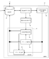
- the inspection apparatus 100 is configured to include a control unit 10 configured by a processing device such as a PC, a monitor 12, and an imaging unit 32. Further, the imaging unit 32 further includes a radiation quality changing unit 14, a radiation generator driving unit 16, a substrate holding unit driving unit 18, a detector driving unit 20, a radiation generator 22, a substrate holding unit 24, and a detector 26. have.
- the radiation generator 22 is a device that generates radiation such as X-rays, and generates radiation by causing accelerated electrons to collide with a target such as tungsten or diamond, for example.
- the substrate holding unit 24 holds a substrate which is an inspection object.
- the substrate held by the substrate holding unit 24 is irradiated with the radiation generated by the radiation generator 22, and the radiation transmitted through the substrate is imaged as an image by the detector 26.
- the radiation transmission image of the substrate captured by the detector 26 is referred to as a “transmission image”.
- the substrate holding unit 24 holding the substrate and the detector 26 are moved relative to the radiation generator 22 to obtain a plurality of transmission images, and a reconstructed image is obtained.
- the transmission image captured by the detector 26 is sent to the control unit 10, and, for example, using a known technique such as a filtered corrected backprojection method (Filtered-Backprojection method (FBP method)) Reconstructed into an image containing a shape. Then, the reconstructed image and the transmission image are stored in a storage in the control unit 10 or an external storage (not shown).
- FBP method Filtered-Backprojection method
- an image reconstructed into a three-dimensional image including the three-dimensional shape of the solder of the joint portion based on the transmission image is referred to as a “reconstructed image”.
- an image obtained by cutting an arbitrary cross section from the reconstructed image is referred to as a "cross-sectional image”.
- Such reconstructed image and cross-sectional image are output to the monitor 12.
- the reconstructed image in the present embodiment is also referred to as “planar CT” because it is reconstructed from the planar image captured by the detector 26 as described above.
- the radiation quality changing unit 14 changes the radiation quality of the radiation generated by the radiation generator 22.
- the radiation quality is determined by the voltage applied to accelerate the electrons to collide with the target (hereinafter referred to as “tube voltage”), and the current that determines the number of electrons (hereinafter referred to as “tube current”).
- the line quality change unit 14 is a device that controls the tube voltage and the tube current.
- the quality change unit 14 can be realized using a known technology such as a transformer or a rectifier.
- the radiation quality is determined by the brightness and hardness of the radiation (the spectral distribution of the radiation). If the tube current is increased, the number of electrons colliding with the target increases and the number of photons of generated radiation also increases. As a result, the luminance of the radiation is increased. For example, some components such as capacitors have a thickness compared to other components, and it is necessary to irradiate radiation with high brightness to capture transmission images of these components. In such a case, the brightness of the radiation is adjusted by adjusting the tube current. Also, when the tube voltage is increased, the energy of electrons colliding with the target is increased, and the energy (spectrum) of the generated radiation is increased. Generally, the greater the energy of the radiation, the greater the penetration of the material, and the less likely it is to be absorbed by the material. Transmission images taken with such radiation have low contrast. Thus, the tube voltage can be used to adjust the contrast of the transmitted image.
- the radiation generator drive unit 16 has a drive mechanism such as a motor (not shown), and can move the radiation generator 22 up and down along an axis passing through its focal point. Thereby, the distance between the radiation generator 22 and the inspection object (substrate) held by the substrate holding unit 24 is changed to change the irradiation field, and the enlargement ratio of the transmission image captured by the detector 26 is changed. It becomes possible.
- the detector drive unit 20 also has a drive mechanism such as a motor (not shown), and rotates the detector 26 along the detector rotation track 30.
- the substrate holding unit driving unit 18 also has a driving mechanism such as a motor (not shown) and moves the substrate holding unit 24 in parallel on the plane on which the substrate rotation track 28 is provided. Further, the substrate holding unit 24 is configured to be rotationally moved on the substrate rotation track 28 in conjunction with the rotational movement of the detector 26. This makes it possible to capture a plurality of transmission images having different projection directions and projection angles while changing the relative positional relationship between the substrate held by the substrate holding unit 24 and the radiation generator 22.
- the rotation radius of the substrate rotation track 28 and the detector rotation track 30 is not fixed but can be freely changed. Thereby, it becomes possible to change arbitrarily the irradiation angle of the radiation irradiated to the components arrange
- the control unit 10 controls all the operations of the inspection apparatus 100 described above. Hereinafter, various functions of the control unit 10 will be described with reference to FIG. Although not shown, the control unit 10 is connected to an input device such as a keyboard and a mouse.
- the control unit 10 includes a storage unit 34, a cross-sectional image generation unit 36, a substrate inspection surface detection unit 38, a pseudo cross-sectional image generation unit 40, and an inspection unit 42. Although not shown, the control unit 10 also includes an imaging control unit that controls the operation of the radiation quality changing unit 14, the radiation generator driving unit 16, the substrate holding unit driving unit 18, and the detector driving unit 20.
- Each of these functional blocks is realized by cooperation of a CPU that executes various arithmetic processing, hardware such as a RAM used as a work area for storing data and executing a program, and software. Therefore, these functional blocks can be realized in various forms by a combination of hardware and software.
- the storage unit 34 stores information such as imaging conditions for capturing a transmission image of a substrate, and a design of a substrate which is an inspection object.
- the storage unit 34 also stores transmission images and reconstructed images (cross-sectional images and pseudo-cross-sectional images) of the substrate, inspection results of the inspection unit 42 described later, and the like.
- the storage unit 34 further controls the speed at which the radiation generator driving unit 16 drives the radiation generator 22, the speed at which the substrate holding unit driving unit 18 drives the substrate holding unit 24, and the detector driving unit 20 drives the detector 26. The speed is also stored.
- the cross-sectional image generation unit 36 generates a cross-sectional image based on the plurality of transmission images acquired from the storage unit 34. This can be realized by using known techniques such as FBP method and maximum likelihood estimation method. Different reconstruction algorithms differ in the nature of the resulting reconstructed image and the time it takes to reconstruct it. Therefore, it is possible to prepare in advance a plurality of reconstruction algorithms and parameters used for the algorithms, and allow the user to select. In this way, it is possible to provide the user with a freedom of choice, such as giving priority to shortening of the time required for reconstruction, or prioritizing good image quality even if it takes time.
- the generated cross-sectional image is output to the storage unit 34 and recorded in the storage unit 34.
- the substrate inspection surface detection unit 38 detects, from among the plurality of cross-sectional images generated by the cross-sectional image generation unit 36, a position (cross-sectional image) showing a surface (for example, the surface of the substrate) on the substrate to be inspected. Identify.
- a cross-sectional image that reflects the inspection surface of the substrate is referred to as an “inspection surface image”. The details of the inspection surface image detection method will be described later.
- the pseudo cross-sectional image generation unit 40 images a region of a substrate thicker than the cross-sectional image by stacking a predetermined number of continuous cross-sectional images on the cross-sectional images generated by the cross-sectional image generation unit 36.
- the number of cross-sectional images to be stacked is determined by the thickness of the region of the substrate from which the cross-sectional image appears (hereinafter referred to as "slice thickness") and the slice thickness of the pseudo cross-sectional image.
- the inspection surface image specified by the substrate inspection surface detection unit 38 is used to specify the position of the solder.
- the inspection unit 42 is a solder joint state based on the cross-sectional image generated by the cross-sectional image generation unit 36, the inspection surface image specified by the substrate inspection surface detection unit 38, and the pseudo cross-sectional image generated by the pseudo cross-sectional image generation unit 40. To check. Since the solder for joining the substrate and the component is in the vicinity of the inspection surface of the substrate, the solder and the substrate are inspected by inspecting a cross-sectional image showing the region on the radiation generator 22 side on the inspection surface image and the inspection surface image. It can be determined whether or not the parts are properly joined.
- solder bonding state refers to whether or not the substrate and the component are bonded by solder and an appropriate conductive path is generated. Inspection of solder joint state includes bridge inspection, melt state inspection, and void inspection. “Bridge” refers to an undesirable conductive path between conductors created by the joining of solders. Further, the “melted state” refers to a state of whether bonding between the substrate and the component is insufficient due to insufficient melting of the solder, that is, a state of so-called “floating” or not. "Void” refers to a defect in the solder joint due to air bubbles in the solder joint. Therefore, the inspection unit 42 includes a bridge inspection unit 44, a molten state inspection unit 46, and a void inspection unit 48.
- the bridge inspection unit 44 and the void inspection unit 48 are based on the pseudo cross section image generated by the pseudo cross section image generation unit 40.
- the bridge and the void are inspected respectively, and the molten state inspection unit 46 inspects the molten state of the solder based on the inspection surface image specified by the substrate inspection surface detection unit 38.
- the inspection results in the bridge inspection unit 44, the molten state inspection unit 46, and the void inspection unit 48 are recorded in the storage unit 34.
- FIG. 3 is a flow chart showing a flow from imaging of a transmission image and generation of a reconstructed image and identification of an inspection surface image to inspection of a solder bonding state. The process in this flowchart starts, for example, when the control unit 10 receives an instruction to start an examination from an input device (not shown).
- control unit 10 sets the irradiation field of the radiation emitted by the radiation generator 22 by the radiation generator driving unit 16, moves the substrate holding unit 24 by the substrate holding unit driving unit 18, and detects
- the radiation quality is set by the radiation quality changing unit 14 while irradiating the radiation to the substrate to pick up a transmission image while changing the imaging position by moving the detector 26 by the drive unit 20 and changing the imaging position.
- the cross-sectional image generation unit 36 and the pseudo cross-sectional image generation unit 40 generate a reconstructed image (step S10).
- the substrate inspection surface detection unit 38 of the control unit 10 receives the transmission image or the reconstructed image (cross sectional image) from the cross sectional image generation unit 36, and specifies the inspection surface image from among them (step S12).
- the bridge inspection unit 44 acquires, from the pseudo cross-sectional image generation unit 40, a pseudo cross-sectional image having a slice thickness similar to that of the solder ball projecting the solder ball, and inspects for the presence or absence of a bridge (step S14). If the bridge is not detected (“N” in step S16), the molten state inspection unit 46 acquires an inspection surface image from the substrate inspection surface detection unit 38, and inspects whether the solder is molten (step S18). ).
- the void inspection unit 48 acquires a pseudo sectional image partially projecting the solder ball from the pseudo sectional image generation unit 40, and a void exists. It is checked whether or not it is (step S22). If no void is found (“N” in step S24), the void inspection unit 48 determines that the solder bonding state is normal (step S26), and outputs that effect to the storage unit 34.
- step S16 When a bridge is detected ("Y" in step S16), when the solder is not melted ("N” in step S20), or when a void exists ("Y” in step S24), The bridge inspection unit 44, the molten state inspection unit 46, and the void inspection unit 48 determine that the bonding state of the solder is abnormal (step S28), and outputs that effect to the storage unit 34. When the state of the solder is output to the storage unit 34, the process in this flowchart ends.
- a large range including the front surface and the back surface of the substrate (a range in which an error such as the above-described substrate warpage is considered)
- planar CT calculation a three-dimensional image (reconstructed image) including an error such as warpage of the substrate is acquired, and using cross-section design information of the substrate, a plurality of cross-sectional images from this three-dimensional image (reconstructed image)
- a specific pattern or mark shape (specific pattern or mark image) for specifying an inspection position is detected in the X, Y, and Z directions, and a substrate inspection surface (inspection surface image) is determined.
- design information of substrate refers to Gerber data and CAD (Computer Aided Design) data, and is stored in advance in the storage unit 34 described above.
- Information in which the coordinates of the solder joint portion are recorded is called Gerber data, and information in which the coordinates of the type of mounting component and the mounting position are recorded is called CAD data.
- the coordinates of the solder joint portion and the mounting position of the component are described as coordinates of an XY coordinate system set on the substrate.
- the inspection position (inspection surface image) can be specified.
- a substrate surface image serving as a template is registered on each of the front and back sides of the substrate for each FOV (field of view) of the transmission image or for each area obtained by dividing the FOV into 2 ⁇ 2 (Gerber data described above And CAD data can be used). Then, image matching with a template registered in a predetermined XYZ search range is performed for each FOV on each substrate to be imaged, and the position with the highest matching rate is used as the amount of deviation. By detecting the amount of deviation for each FOV or for each area obtained by dividing the FOV in this manner, one or four deviation amounts for one FOV can be obtained, as shown in FIG. The amount of deviation is expressed as the apex of a triangle with respect to the entire substrate.
- the correction amount is calculated from the deviation amount of the apex of the triangle (the deviation amount from the reference plane is calculated), and the inspection is performed based on this correction amount Determine the plane image.
- the displacement amount of the apex of the triangle it is possible to correct the shift in the XYZ directions and the rotation with respect to the XYZ axes.
- a cross-sectional image is determined from the above error according to each inspection point, a pseudo cross-sectional image is generated using it, inspection is performed, and the same processing is performed by moving to the next inspection point. Do.
- position correction is individually performed on an inspection target component that requires high-accuracy position correction. At this time, since the substrate surface is roughly detected by image matching in advance, the search range is limited and processing can be performed at high speed.
- a three-dimensional image reconstruction of a range in which an error such as warpage of the substrate is taken into consideration The image
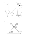
- the method of specifying the inspection position (substrate inspection surface) according to the second embodiment is as shown in FIG.
- a shape (transmission image) IA1, IA2 of an image of a specific pattern or mark is detected in two or more transmission images, and a three-dimensional image (reconstruction image) is detected based on the XYZ position of the transmission image in each of these transmission images.
- To determine the position of a specific pattern or mark shape an image of a specific pattern or mark in a three-dimensional image
- a method of specifying the position of A (the position where the three-dimensional image A of a specific pattern or mark is present in the reconstruction space (reconstruction image)) will be described.
- the substrate substrate holding unit 24
- the detector 26 with respect to the fixed radiation source (radiation generator 22).
- the radiation angle of the radiation is changed by moving the radiation relative to the substrate to capture a plurality of transmission images, but in FIG.
- the substrate to be inspected is fixed, and the radiation source It shows about the case where the device 22) and the detector 26 are moved.
- the positions (coordinates) in FIG. 6 indicate the positions of the radiation source (the radiation generator 22), the substrate (the substrate holding unit 24), and the detector 26 in the inspection apparatus 100 (the positions from the predetermined origin of the inspection apparatus 100). It can be obtained by calculation using Further, in FIG. 6, a position (reference point) as a reference is O.
- the position of the radiation source at the first projection angle (coordinates at which radiation is emitted from the radiation generator 22) is (SX1, SY1, SZ1), and the detector 26 detects the transmitted image IA1 of a specific pattern or mark Let the given position be (DX1, DY1, DZ1) and let the position of the image A of this particular pattern or mark in the reconstructed image be (OX, OY, OZ). Further, the position of the radiation source at the second projection angle is (SX2, SY2, SZ2), and the position of the transmission image IA2 at the detector 26 is (DX2, DY2, DZ2).
- the positions OX and OY of the image A of a specific pattern or mark in the reconstructed image in the X and Y directions are coordinates on the radiation source and detector on the XY plane, as shown in FIG.
- the point which intersects the straight line which connected with should just be calculated
- OY (SY1-DY1) / (SX1-DX1) OX + (SX1, DY1-SY1, DX1) / (SX1-DX1) (1)
- OY (SY2-DY2) / (SX2-DX2) OX + (SX2, DY2-SY2, DX2) / (SX2-DX2) (2)
- OZ which is the position in the Z direction of the image A of a specific pattern or mark in the reconstructed image
- the inspection position (inspection surface image in the reconstructed image) on the substrate is specified from the plurality of transmission images acquired in step S10. Specifically, the shape of the transmission image of a specific pattern or mark in the transmission image is detected by image matching or the like, and the position of the pattern or mark in the reconstructed image is determined from the position using the above equation to perform inspection.
- the inspection can be performed using the inspection plane image (sectional image) of the correct position.
- the inspection position (inspection surface image) is not specified from the entire three-dimensional image (reconstructed image), but is specified from the transmission image of a smaller amount of data, the time for specification is shortened.
- the shape of the specific pattern or mark (the shape of the transmission image) in the vicinity of each inspection position or inspection position is registered, and the position in the transmission image is specified by image matching for each. By doing this, the position (inspection surface image) in the reconstructed image can also be identified.
- a pseudo cross-sectional image can be generated in consideration of not only the Z direction but also the position in the XY directions and rotation with respect to the XYZ axes. Furthermore, a pseudo-cross-sectional image in consideration of the deflection of the object is generated by referring to the positions of four or more specific patterns or marks and using known interpolation methods such as linear interpolation, parabolic interpolation, cubic interpolation, etc. Can.
- a reconstruction image is generated, and in step S12 a substrate inspection surface using the transmission image or the reconstruction image
- the inspection position (substrate inspection surface) in the reconstruction space is identified from the transmission image, and the reconstructed image (the identified position) is identified (see FIG. 7). This is a configuration for reconstructing a reconstructed image (containing a specific pattern or mark).
- FIG. 8 shows a flowchart for inspecting the bonding state of the solder in the third embodiment, and the same processes as the processes described above are denoted by the same reference numerals and detailed description thereof will be omitted.
- the control unit 10 sets the radiation field of the radiation emitted by the radiation generator 22 by the radiation generator driving unit 16 as described above, and the substrate holding unit by the substrate holding unit driving unit 18 24 while moving the detector 26 and moving the detector 26 by the detector driving unit 20 to change the imaging position, the radiation quality of the radiation generator 22 is set by the radiation quality changing unit 14 and radiation is applied to the substrate A transmission image is taken (step S11).
- the position of the image to be inspected in these transmission images is specified by image matching or the like, and from the position thus specified, ,
- the position in the reconstruction space (reconstruction image) is specified (step S12).
- a reconstructed image (inspection surface image or cross-sectional image) including the position specified in step S12 is generated (step S13).
- the inspection of the bonding state of the solder based on this reconstructed image is as described above (steps S14 to S28).
- the generation of the reconstructed image is limited to the part including the inspection target, so the amount of data of the reconstructed image is reduced, which results in a time for generation of the reconstructed image. As a result, the entire examination time can be shortened.
Abstract
被検査対象における検査面の位置(Z方向位置)を予め特定することなく正確な検査を行うことができる検査位置の特定方法、及び、被検査対象における検査面の位置(Z方向位置)を予め特定することなく検査に必要な3次元画像を生成して検査を行うことができる3次元画像の生成方法、並びにこれらの方法を有する検査装置を提供する。 検査装置100は、被検査体(基板)の放射線透過画像及びこの放射線透過画像から生成された3次元画像を記憶する記憶部34と、制御部10と、を有し、制御部10の3次元画像における検査位置を特定する処理は、放射線透過画像において、検査位置の透過像の位置を特定するステップと、透過像の位置から、3次元画像における検査位置を特定するステップと、を有する。
Description
本発明は、被検査体を検査する際の検査位置の特定方法、3次元画像の生成方法、及び、これらの方法を有する検査装置に関する。
基板表面や裏面のはんだ形状を計測する検査装置として、トモシンセシス方式のX線検査装置がある(例えば、特許文献1参照)。
しかしながら、このようなX線検査装置では、予めレーザー測長器などでZ方向(X線投射方向若しくは基板表面に対する高さ方向)の基板表面や裏面の位置を特定しておき、その高さでの断面画像を再構成する、または、再構成された断面画像の中で最適なZ方向の画像を抽出する必要があり、検査時間が長くなるという課題があった。
本発明はこのような課題に鑑みてなされたものであり、被検査対象における検査面の位置(Z方向位置)を予め特定することなく正確な検査を行うことができる検査位置の特定方法、被検査対象における検査面の位置(Z方向位置)を予め特定することなく検査に必要な3次元画像を生成して検査を行うことができる3次元画像の生成方法、及び、これらの方法を有する検査装置を提供することを目的とする。
前記課題を解決するために、第1の本発明に係る検査位置の特定方法は、被検査体の放射線透過画像から生成された3次元画像における検査位置を特定する特定方法であって、放射線透過画像において、検査位置の透過像の位置を特定するステップと、透過像の位置から、3次元画像における検査位置を特定するステップと、を有することを特徴とする。
また、このような本発明に係る検査位置の特定方法において、透過像の位置を特定するステップは、検査位置または検査位置の近傍の特定のパターンやマークの透過像の形状を用いて特定することが好ましい。
また、本発明に係る検査装置は、放射線透過画像及び3次元画像を記憶する記憶部と、記憶部から放射線透過画像を取り出して、上述した検査位置の特定方法により、3次元画像における検査位置を特定する制御部と、を有することを特徴とする。
また、第2の本発明に係る3次元画像の生成方法は、被検査体の放射線透過画像から前記被検査体の3次元画像を生成する生成方法であって、放射線透過画像において、被検査体の検査位置の透過像の位置を特定するステップと、透過像の位置から、3次元画像における検査位置を特定するステップと、放射線透過画像から、検査位置を含む被検査体の3次元画像を生成するステップと、を有することを特徴とする。
また、本発明に係る3次元画像の生成方法において、透過像の位置を特定するステップは、検査位置または検査位置の近傍の特定のパターンやマークの透過像の形状を用いて特定することが好ましい。
また、本発明に係る検査装置は、放射線透過画像及び3次元画像を記憶する記憶部と、記憶部から放射線透過画像を取り出して、上述した3次元画像の生成方法により、被検査体の3次元画像を生成する制御部と、を有することを特徴とする。
本発明に係る検査位置の特定方法によれば、被検査対象における検査面の位置(Z方向位置)を予め特定することなく、正確な検査を行うことができる。
以下、本発明の好ましい実施形態について図面を参照して説明する。図1に示すように、本実施形態に係る検査装置100は、PC等の処理装置で構成される制御部10、モニタ12、及び、撮像部32を有して構成されている。また、撮像部32は、更に、線質変更部14、放射線発生器駆動部16、基板保持部駆動部18、検出器駆動部20、放射線発生器22、基板保持部24、及び、検出器26を有している。
放射線発生器22は、X線等の放射線を発生させる装置であり、例えば加速させた電子をタングステンやダイアモンド等のターゲットに衝突させることで放射線を発生するものである。
基板保持部24は、被検査体である基板を保持する。基板保持部24に保持された基板に放射線発生器22で発生させた放射線を照射し、基板を透過した放射線を検出器26で画像として撮像する。以下、検出器26で撮像された基板の放射線透過画像を「透過画像」と呼ぶ。なお、後述するように、本実施形態においては、基板を保持した基板保持部24と検出器26とを放射線発生器22に対して相対移動させて複数の透過画像を取得して、再構成画像を生成する。
検出器26で撮像された透過画像は、制御部10に送られ、例えば、フィルタ補正逆投影法(Filtered-Backprojection法(FBP法))等の既知の技術を用いて、接合部分のはんだの立体形状を含む画像に再構成される。そして、再構成された画像や透過画像は、制御部10内のストレージや、図示しない外部のストレージに記憶される。以下、透過画像に基づいて接合部分のはんだの立体形状を含む3次元画像に再構成された画像を「再構成画像」と呼ぶ。また、再構成画像から任意の断面を切り出した画像を「断面画像」と呼ぶ。このような再構成画像及び断面画像はモニタ12に出力される。なお、モニタ12には再構成画像や断面画像のみならず、後述するはんだの接合状態の検査結果等も表示される。また、本実施形態における再構成画像は、上述したように、検出器26で撮像された平面画像から再構成されるため「プラナーCT」とも呼ぶ。
線質変更部14は、放射線発生器22で発生される放射線の線質を変更する。放射線の線質は、ターゲットに衝突させる電子を加速するために印加する電圧(以下「管電圧」と呼ぶ)や、電子の数を決定する電流(以下「管電流」と呼ぶ)によって定まる。線質変更部14は、これら管電圧と管電流とを制御する装置である。この線質変更部14は変圧器や整流器等、既知の技術を用いて実現できる。
ここで、放射線の線質は、放射線の輝度と硬さ(放射線のスペクトル分布)とで定まる。管電流を大きくすればターゲットに衝突する電子の数が増え、発生する放射線の光子の数も増える。その結果、放射線の輝度が大きくなる。例えば、コンデンサ等の部品の中には他の部品と比較して厚みがあるものもあり、これらの部品の透過画像を撮像するには輝度の大きな放射線を照射する必要がある。このような場合に管電流を調整することで放射線の輝度を調整する。また、管電圧を高くすると、ターゲットに衝突する電子のエネルギーが大きくなり、発生する放射線のエネルギー(スペクトル)が大きくなる。一般に、放射線のエネルギーが大きいほど物質の貫通力が大きくなり、物質に吸収されにくくなる。そのような放射線を用いて撮像した透過画像はコントラストが低くなる。このため、管電圧は透過画像のコントラストを調整するのに利用できる。
放射線発生器駆動部16は、図示しないモータ等の駆動機構を有しており、放射線発生器22をその焦点を通る軸に沿って上下に移動させることができる。これにより放射線発生器22と基板保持部24に保持される被検査体(基板)との距離を変えて照射野を変更し、検出器26で撮像される透過画像の拡大率を変更することが可能となる。
検出器駆動部20も図示しないモータ等の駆動機構を有しており、検出器回転軌道30に沿って検出器26を回転移動させる。また、基板保持部駆動部18も図示しないモータ等の駆動機構を有しており、基板回転軌道28が設けられた平面上を、基板保持部24を平行移動させる。また、基板保持部24は、検出器26の回転移動と連動して、基板回転軌道28上を回転移動する構成となっている。これにより、基板保持部24が保持する基板と放射線発生器22との相対的な位置関係を変更させながら、投射方向及び投射角度が異なる複数の透過画像を撮像することが可能となる。
ここで、基板回転軌道28と検出器回転軌道30との回転半径は固定ではなく、自由に変更できる構成となっている。これにより、基板に配置される部品に照射する放射線の照射角度を任意に変更することが可能となる。
制御部10は、上述した検査装置100の全動作を制御する。以下、制御部10の諸機能について図2を用いて説明する。なお、図示されていないが、制御部10にはキーボードおよびマウスなどの入力装置が接続されている。
制御部10は、記憶部34、断面画像生成部36、基板検査面検出部38、疑似断面画像生成部40、及び検査部42を含む。なお、図示しないが制御部10は線質変更部14、放射線発生器駆動部16、基板保持部駆動部18、及び検出器駆動部20の作動を制御する撮像制御部も含む。また、これらの各機能ブロックは、各種演算処理を実行するCPU、データの格納やプログラム実行のためのワークエリアとして利用されるRAMなどのハードウェア、およびソフトウェアの連携によって実現される。したがって、これらの機能ブロックはハードウェアおよびソフトウェアの組み合わせによって様々な形で実現することができる。
記憶部34は、基板の透過画像を撮像するための撮像条件や、被検査体である基板の設計等の情報を記憶する。記憶部34はまた、基板の透過画像や再構成画像(断面画像、疑似断面画像)、及び後述する検査部42の検査結果等を記憶する。記憶部34はさらに、放射線発生器駆動部16が放射線発生器22を駆動する速度、基板保持部駆動部18が基板保持部24を駆動する速度および検出器駆動部20が検出器26を駆動する速度も格納されている。
断面画像生成部36は、記憶部34から取得した複数の透過画像に基づいて、断面画像を生成する。これは、例えばFBP法や最尤推定法等、既知の技術を用いて実現できる。再構成アルゴリズムが異なると、得られる再構成画像の性質や再構成に要する時間も異なる。そこで、あらかじめ複数の再構成アルゴリズムやアルゴリズムに用いられるパラメータを用意しておき、ユーザに選択させる構成としてもよい。これにより、再構成に要する時間が短くなることを優先したり、時間はかかっても画質の良さを優先したりするなどの選択の自由度をユーザに提供することができる。生成した断面画像は記憶部34に出力し、この記憶部34に記録される。
基板検査面検出部38は、断面画像生成部36が生成した複数の断面画像の中から、基板上の検査の対象となる面(例えば、基板の表面)を映し出している位置(断面画像)を特定する。以後、基板の検査面を映し出している断面画像を「検査面画像」という。検査面画像の検出方法についての詳細は後述する。
疑似断面画像生成部40は、断面画像生成部36が生成した断面画像について、連続する所定枚数の断面画像を積み上げることにより、断面画像よりも厚い基板の領域を画像化する。積み上げる断面画像の枚数は、断面画像が映し出す基板の領域の厚さ(以後、「スライス厚」という。)と、疑似断面画像のスライス厚とによって定める。例えば、断面画像のスライス厚が50μmで、疑似断面画像としてBGAのはんだボール(以後単に「はんだ」という。)の高さ(例えば500μm)をスライス厚としようとするならば、500/50=10枚の断面画像を積み上げればよい。この際、はんだの位置を特定するために、基板検査面検出部38が特定した検査面画像が用いられる。
検査部42は、断面画像生成部36が生成した断面画像、基板検査面検出部38が特定した検査面画像、及び疑似断面画像生成部40が生成した疑似断面画像に基づいて、はんだの接合状態を検査する。基板と部品とを接合するはんだは基板検査面付近にあるので、検査面画像及び検査面画像に対して放射線発生器22側の領域を映し出している断面画像を検査することで、はんだが基板と部品とを適切に接合しているか否かが判断できる。
ここで、「はんだの接合状態」とは、基板と部品とがはんだにより接合し、適切な導電経路が生成されているか否かのことをいう。はんだの接合状態の検査には、ブリッジ検査、溶融状態検査、及びボイド検査が含まれる。「ブリッジ(bridge)」とは、はんだが接合することにより生じた導体間の好ましくない導電経路のことをいう。また、「溶融状態」とは、はんだの溶融不足により、基板と部品との間の接合が不足しているか否かの状態、いわゆる「浮き」か否かの状態をいう。「ボイド(void)」とは、はんだ接合部内の気泡によるはんだ接合の不具合のことをいう。したがって検査部42は、ブリッジ検査部44、溶融状態検査部46、及びボイド検査部48を含む。
ブリッジ検査部44、溶融状態検査部46、及びボイド検査部48の動作の詳細は後述するが、ブリッジ検査部44およびボイド検査部48は、疑似断面画像生成部40が生成した疑似断面画像に基づいてそれぞれブリッジおよびボイドの検査をし、溶融状態検査部46は基板検査面検出部38が特定した検査面画像に基づいてはんだの溶融状態を検査する。なお、ブリッジ検査部44、溶融状態検査部46、及びボイド検査部48における検査結果は記憶部34に記録される。
図3は透過画像の撮像及び再構成画像の生成、及び、検査面画像の特定から、はんだの接合状態を検査するまでの流れを示したフローチャートである。本フローチャートにおける処理は、例えば、制御部10が図示しない入力装置から検査開始の指示を受け付けたときに開始する。
制御部10は、上述したように、放射線発生器駆動部16により放射線発生器22により放射される放射線の照射野を設定し、基板保持部駆動部18により基板保持部24を移動させるとともに、検出器駆動部20により検出器26を移動させて撮像位置を変更しながら、線質変更部14により放射線発生器22の線質を設定して放射線を基板に照射して透過画像を撮像し、さらに、このようにして撮像された複数枚の透過画像から、断面画像生成部36及び疑似断面画像生成部40により再構成画像を生成する(ステップS10)。
次に、制御部10の基板検査面検出部38は、断面画像生成部36から透過画像または再構成画像(断面画像)を受け取り、その中から検査面画像を特定する(ステップS12)。ブリッジ検査部44は、疑似断面画像生成部40からはんだボールを映し出しているはんだボールと同程度のスライス厚の疑似断面画像を取得し、ブリッジの有無を検査する(ステップS14)。ブリッジを検出しない場合には(ステップS16の「N」)、溶融状態検査部46は基板検査面検出部38から検査面画像を取得し、はんだが溶融しているか否かを検査する(ステップS18)。はんだが溶融している場合には(ステップS20の「Y」)、ボイド検査部48は疑似断面画像生成部40からはんだボールを部分的に映し出している疑似断面画像を取得し、ボイドが存在するか否かを検査する(ステップS22)。ボイドが見つからない場合には(ステップS24の「N」)、ボイド検査部48は、はんだの接合状態は正常と判断し(ステップS26)、その旨を記憶部34に出力する。また、ブリッジを検出した場合(ステップS16の「Y」)、はんだが溶融していない場合(ステップS20の「N」)、またはボイドが存在する場合には(ステップS24の「Y」)、それぞれブリッジ検査部44、溶融状態検査部46、およびボイド検査部48ははんだの接合状態は異常と判断して(ステップS28)その旨を記憶部34に出力する。はんだの状態が記憶部34に出力されると、本フローチャートにおける処理は終了する。
上述したように、透過画像から再構成された3次元画像である再構成画像(再構成空間)内には、傾き、ずれ、たわみ、回転、伸縮等を起因とする誤差を有した基板の画像データが存在している。そのため、自動検査を行うためには、これらの誤差を考慮した位置補正を行い、この位置補正に基づいて検査面画像を特定する必要がある。以下に、基板検査面検出処理S12における検査位置(基板検査面)の特定方法(誤差の補正方法)について説明する。
(第1の実施形態)
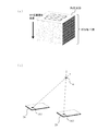
検査位置の特定方法の第1の実施形態は、上述した再構成画像の生成(ステップS10)において、基板の表面と裏面を含む大きな範囲(上述した基板の反り等の誤差を考慮した範囲)でプラナーCT演算を行うことで、基板の反り等の誤差を含む三次元画像(再構成画像)を取得し、基板の設計情報を用いて、この三次元画像(再構成画像)から複数の断面画像に跨がってXYZ方向に、検査位置を特定するための特定のパターンやマークの形状(特定のパターンやマークの像)を検出して、基板検査面(検査面画像)の決定を行う。
検査位置の特定方法の第1の実施形態は、上述した再構成画像の生成(ステップS10)において、基板の表面と裏面を含む大きな範囲(上述した基板の反り等の誤差を考慮した範囲)でプラナーCT演算を行うことで、基板の反り等の誤差を含む三次元画像(再構成画像)を取得し、基板の設計情報を用いて、この三次元画像(再構成画像)から複数の断面画像に跨がってXYZ方向に、検査位置を特定するための特定のパターンやマークの形状(特定のパターンやマークの像)を検出して、基板検査面(検査面画像)の決定を行う。
ここで「基板の設計情報」とは、ガーバーデータ(Gerber data)およびCAD(Computer Aided Design)データのことをいい、上述した記憶部34にあらかじめ記憶しておく。はんだ接合部分の座標を記録した情報をガーバーデータといい、搭載部品の種類および搭載位置の座標を記録した情報をCADデータという。はんだの接合部分および部品の搭載位置の座標は基板上に設定されたXY座標系の座標として記載される。ガーバーデータおよびCADデータを参照することで、再構成画像(断面画像)に対するイメージマッチング(パターンマッチング)等を行うことにより、基板上に存在する部品の種類やその大きさ、部品やはんだ接合部分の位置を得る、すなわち、検査位置(検査面画像)を特定することができる。
具体的には、透過画像のFOV(Field of View:視野)毎、またはFOVを2×2に4分割した領域毎にテンプレートとなる基板表面画像を基板の裏表それぞれで登録する(上述したガーバーデータやCADデータを用いることができる)。そして、撮像する各基板でFOV毎に所定のXYZサーチ範囲において登録したテンプレートとイメージマッチングを行い、最も一致率の高い位置をずれ量として用いる。このようにFOV毎、若しくはFOVを4分割した領域毎にずれ量を検出することにより、1枚のFOVに対して1個または4個のずれ量を有することになり、図4に示すように、このずれ量は、基板全体に対して、三角形の頂点として表現される。そして、それぞれの三角形で囲まれた領域の検査を行う際には三角形の頂点のずれ量から補正量を計算し(基準となる面からのずれ量を計算する)、この補正量に基づいて検査面画像を決定する。三角形の頂点のずれ量を用いることで、XYZ方向のシフト及びXYZ軸に対する回転の補正が可能となる。検査箇所が複数ある場合に、それぞれの検査箇所に応じて上記誤差から断面画像を決定し、それを用いて疑似断面画像を生成して、検査し、次の検査箇所に移って同様の処理を行う。また、更に、高精度な位置補正が必要な検査対象部品に関しては、個別に位置補正を行う。この際には先にイメージマッチングで大まかには基板表面を検出しているので、サーチ範囲は限られ高速に処理を行うことができる。
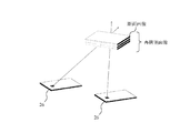
(第2の実施形態)
図5(a)に示すように、第1の実施形態に係る検査位置(基板検査面)の特定方法は、透過画像から、基板の反り等の誤差を考慮した範囲の3次元画像(再構成画像)を再構成し、この3次元画像を用いて特定していたが、この第2の実施形態に係る検査位置(基板検査面)の特定方法は、図5(b)に示すように、2以上の透過画像において特定のパターンやマークの像の形状(透過像)IA1,IA2を検出し、これらの透過画像の各々における透過像のXYZの位置に基づいて、3次元画像(再構成画像)における特定のパターンやマークの形状(3次元画像における特定のパターンやマークの像)Aの位置を特定して検査面画像を決定する方法である。
図5(a)に示すように、第1の実施形態に係る検査位置(基板検査面)の特定方法は、透過画像から、基板の反り等の誤差を考慮した範囲の3次元画像(再構成画像)を再構成し、この3次元画像を用いて特定していたが、この第2の実施形態に係る検査位置(基板検査面)の特定方法は、図5(b)に示すように、2以上の透過画像において特定のパターンやマークの像の形状(透過像)IA1,IA2を検出し、これらの透過画像の各々における透過像のXYZの位置に基づいて、3次元画像(再構成画像)における特定のパターンやマークの形状(3次元画像における特定のパターンやマークの像)Aの位置を特定して検査面画像を決定する方法である。
図6により、2枚の透過画像において、特定のパターンやマークの透過像(ここでは、点IA1,IA2として説明する)が検出された位置から、再構成画像上の特定のパターンやマークの像Aの位置(再構成空間(再構成画像)において、特定のパターンやマークの3次元像Aがある位置)を特定する方法について説明する。なお、図1に示すように、本実施形態に係る検査装置100においては、固定された放射線源(放射線発生器22)に対して、検査対象の基板(基板保持部24)と検出器26とを相対移動させることにより、基板に対する放射線の投射角を変化させて複数枚の透過画像を撮像しているが、図6(a)においては、検査対象の基板を固定とし、放射線源(放射線発生器22)及び検出器26を移動させた場合について示している。なお、この図6における位置(座標)は、放射線源(放射線発生器22)、基板(基板保持部24)及び検出器26の検査装置100における位置(検査装置100の所定の原点からの位置)を用いて、計算により求めることができる。また、図6において、基準となる位置(基準点)をOとする。
まず、第1の投射角における放射線源の位置(放射線発生器22から放射線が放射される座標)を(SX1,SY1,SZ1)とし、検出器26において特定のパターンやマークの透過像IA1が検出された位置を(DX1,DY1,DZ1)とし、再構成画像内のこの特定のパターンやマークの像Aの位置を(OX,OY,OZ)とする。また、第2の投射角における放射線源の位置を(SX2,SY2,SZ2)とし、検出器26における透過像IA2の位置を(DX2,DY2,DZ2)とする。再構成画像内の特定のパターンやマークの像AのX方向及びY方向の位置であるOX,OYは、図6(b)に示すように、XY平面上で放射線源と検出器上の座標とを結んだ直線を交わる点を求めればよく、以下の連立方程式(1),(2)をOX,OYについて解くことにより求められる。
OY = (SY1-DY1)/(SX1-DX1)・OX
+ (SX1・DY1-SY1・DX1)/(SX1-DX1) (1)
OY = (SY2-DY2)/(SX2-DX2)・OX
+ (SX2・DY2-SY2・DX2)/(SX2-DX2) (2)
+ (SX1・DY1-SY1・DX1)/(SX1-DX1) (1)
OY = (SY2-DY2)/(SX2-DX2)・OX
+ (SX2・DY2-SY2・DX2)/(SX2-DX2) (2)
また、再構成画像内の特定のパターンやマークの像AのZ方向の位置であるOZは、上述した式(1),(2)より求められたOXの値を用いて、次式(3)により求めることができる。
OZ = (SZ1-DZ1)/(SX1-DX1)・(OX-DX1) (3)
このように、この第2の実施形態の基板検査面検出処理S12においては、ステップS10で取得された複数の透過画像から、基板上の検査位置(再構成画像における検査面画像)を特定する、具体的には、透過画像において特定のパターンやマークの透過像の形状をイメージマッチング等で検出し、その位置から上述の式を用いて再構成画像内のパターンやマークの位置を決定して検査面画像を特定することにより、正確な位置の検査面画像(断面画像)を用いて検査を行うことができる。また、検査位置(検査面画像)を3次元画像(再構成画像)全体から特定するのではなく、より少ないデータ量の透過画像から特定しているため、特定のための時間が短くなり、結果として検査時間全体を短くすることができる。なお、検査対象が複数箇所ある場合は、それぞれの検査箇所または検査箇所近傍の特定のパターンやマークの形状(透過像の形状)を登録しておき、それぞれについてイメージマッチングで透過画像における位置を特定することにより、再構成画像における位置(検査面画像)も特定することができる。
なお、3点の特定のパターンやマークの位置を参照することにより、Z方向のみではなく、XY方向の位置およびXYZ軸に対する回転を考慮して擬似断面画像を生成することができる。さらに、4点以上の特定のパターンやマークの位置を参照し、線形補間、放物線補間、キュービック補間などの既知の補間方法を用いることにより、対象物のたわみを考慮した擬似断面画像を生成することができる。
(第3の実施形態)
第1及び第2の実施形態では、図3に示すように、ステップS10で透過画像を撮影したのち、再構成画像を生成し、ステップS12で、透過画像若しくは再構成画像を用いて基板検査面を特定していたが、第3の実施形態では、図7に示すように、透過画像から再構成空間内における検査位置(基板検査面)を特定し、特定された位置を含む再構成画像(特定のパターンやマークを含む再構成画像)を再構成する構成である。
第1及び第2の実施形態では、図3に示すように、ステップS10で透過画像を撮影したのち、再構成画像を生成し、ステップS12で、透過画像若しくは再構成画像を用いて基板検査面を特定していたが、第3の実施形態では、図7に示すように、透過画像から再構成空間内における検査位置(基板検査面)を特定し、特定された位置を含む再構成画像(特定のパターンやマークを含む再構成画像)を再構成する構成である。
図8は、この第3の実施形態におけるはんだの接合状態を検査するフローチャートを示しており、上述した処理と同じ処理は同じ符号を付すことにより詳細な説明は省略する。制御部10は、検査が開始されると、上述したように、放射線発生器駆動部16により放射線発生器22により放射される放射線の照射野を設定し、基板保持部駆動部18により基板保持部24を移動させるとともに、検出器駆動部20により検出器26を移動させて撮像位置を変更しながら、線質変更部14により放射線発生器22の線質を設定して放射線を基板に照射して透過画像を撮像する(ステップS11)。次に、これらの透過画像を用いて、第2の実施形態で説明したように、これらの透過画像における検査対象の像の位置をイメージマッチング等で特定し、このようにして特定された位置から、再構成空間(再構成画像)における位置を特定する(ステップS12)。そして、ステップS12で特定された位置が含まれる再構成画像(検査面画像または断面画像)を生成する(ステップS13)。この再構成画像によるはんだの接合状態の検査は、上述した通りである(ステップS14~S28)。
この第3の実施形態によると、再構成画像の生成は、検査対象が含まれる部分に限定されるため、再構成画像のデータ量が小さくなり、これにより再構成画像の生成のための時間が短くなり、結果として検査時間全体を短くすることができる。
10 制御部
34 記憶部
100 検査装置
34 記憶部
100 検査装置
Claims (6)
- 被検査体の放射線透過画像から生成された3次元画像における検査位置を特定する特定方法であって、
前記放射線透過画像において、前記検査位置の透過像の位置を特定するステップと、
前記透過像の位置から、前記3次元画像における前記検査位置を特定するステップと、を有することを特徴とする検査位置の特定方法。 - 前記透過像の位置を特定するステップは、前記検査位置または前記検査位置の近傍の特定のパターンやマークの透過像の形状を用いて特定することを特徴とする請求項1に記載の検査位置の特定方法。
- 前記放射線透過画像及び前記3次元画像を記憶する記憶部と、
前記記憶部から前記放射線透過画像を取り出して、請求項1または2に記載の検査位置の特定方法により、前記3次元画像における前記検査位置を特定する制御部と、を有することを特徴とする検査装置。 - 被検査体の放射線透過画像から前記被検査体の3次元画像を生成する生成方法であって、
前記放射線透過画像において、前記被検査体の検査位置の透過像の位置を特定するステップと、
前記透過像の位置から、前記3次元画像における前記検査位置を特定するステップと、
前記放射線透過画像から、前記検査位置を含む前記被検査体の3次元画像を生成するステップと、を有することを特徴とする3次元画像の生成方法。 - 前記透過像の位置を特定するステップは、前記検査位置または前記検査位置の近傍の特定のパターンやマークの透過像の形状を用いて特定することを特徴とする請求項4に記載の検査位置の特定方法。
- 前記放射線透過画像及び前記3次元画像を記憶する記憶部と、
前記記憶部から前記放射線透過画像を取り出して、請求項4または5に記載の3次元画像の生成方法により、前記被検査体の3次元画像を生成する制御部と、を有することを特徴とする検査装置。
Priority Applications (5)
| Application Number | Priority Date | Filing Date | Title |
|---|---|---|---|
| EP18861635.3A EP3690428A4 (en) | 2017-09-28 | 2018-09-26 | INSPECTION POSITION SPECIFICATION PROCESS, THREE-DIMENSIONAL IMAGE GENERATION PROCESS AND INSPECTION DEVICE |
| US16/652,016 US11422099B2 (en) | 2017-09-28 | 2018-09-26 | Inspection position identification method, three-dimensional image generation method, and inspection device |
| CN201880063370.6A CN111247424A (zh) | 2017-09-28 | 2018-09-26 | 检查位置确定方法、三维图像生成方法以及检查装置 |
| CN202311761937.6A CN117871557A (zh) | 2017-09-28 | 2018-09-26 | 检查装置、以及检查区域的确定方法 |
| US17/804,587 US11835475B2 (en) | 2017-09-28 | 2022-05-30 | Inspection position identification method, three-dimensional image generation method, and inspection device |
Applications Claiming Priority (4)
| Application Number | Priority Date | Filing Date | Title |
|---|---|---|---|
| JP2017187451A JP2019060809A (ja) | 2017-09-28 | 2017-09-28 | 3次元画像の生成方法及び検査装置 |
| JP2017-187451 | 2017-09-28 | ||
| JP2017-187450 | 2017-09-28 | ||
| JP2017187450A JP6676023B2 (ja) | 2017-09-28 | 2017-09-28 | 検査位置の特定方法及び検査装置 |
Related Child Applications (2)
| Application Number | Title | Priority Date | Filing Date |
|---|---|---|---|
| US16/652,016 A-371-Of-International US11422099B2 (en) | 2017-09-28 | 2018-09-26 | Inspection position identification method, three-dimensional image generation method, and inspection device |
| US17/804,587 Continuation US11835475B2 (en) | 2017-09-28 | 2022-05-30 | Inspection position identification method, three-dimensional image generation method, and inspection device |
Publications (1)
| Publication Number | Publication Date |
|---|---|
| WO2019065701A1 true WO2019065701A1 (ja) | 2019-04-04 |
Family
ID=65901892
Family Applications (1)
| Application Number | Title | Priority Date | Filing Date |
|---|---|---|---|
| PCT/JP2018/035606 WO2019065701A1 (ja) | 2017-09-28 | 2018-09-26 | 検査位置の特定方法、3次元画像の生成方法、及び検査装置 |
Country Status (4)
| Country | Link |
|---|---|
| US (2) | US11422099B2 (ja) |
| EP (1) | EP3690428A4 (ja) |
| CN (2) | CN117871557A (ja) |
| WO (1) | WO2019065701A1 (ja) |
Families Citing this family (3)
| Publication number | Priority date | Publication date | Assignee | Title |
|---|---|---|---|---|
| CN117871557A (zh) * | 2017-09-28 | 2024-04-12 | 株式会社先机 | 检查装置、以及检查区域的确定方法 |
| DE102019102231A1 (de) * | 2019-01-29 | 2020-08-13 | Senswork Gmbh | Vorrichtung zur Erfassung einer dreidimensionalen Struktur |
| CN113554626A (zh) * | 2021-07-26 | 2021-10-26 | 朗华全能自控设备(上海)股份有限公司 | 一种软性电路板瑕疵检测方法及装置 |
Citations (5)
| Publication number | Priority date | Publication date | Assignee | Title |
|---|---|---|---|---|
| JP2003514233A (ja) * | 1999-11-08 | 2003-04-15 | ニコレット イメージング システムズ | 垂直スライスイメージングを利用した検査方法 |
| JP2005233760A (ja) * | 2004-02-19 | 2005-09-02 | Toshiba It & Control Systems Corp | トモシンセシス装置 |
| JP2008026334A (ja) | 2007-09-04 | 2008-02-07 | Nagoya Electric Works Co Ltd | X線検査装置、x線検査方法およびx線検査プログラム |
| JP2011149737A (ja) * | 2010-01-19 | 2011-08-04 | Saki Corp:Kk | 検査装置 |
| JP2011247588A (ja) * | 2010-05-21 | 2011-12-08 | Hitachi Ltd | 配管検査装置および配管検査方法 |
Family Cites Families (23)
| Publication number | Priority date | Publication date | Assignee | Title |
|---|---|---|---|---|
| US5550376A (en) * | 1995-05-22 | 1996-08-27 | General Electric Company | Method of calibration of imaging devices |
| US6996265B1 (en) * | 1999-11-08 | 2006-02-07 | Teradyne, Inc. | Inspection method utilizing vertical slice imaging |
| US7013038B1 (en) * | 1999-11-08 | 2006-03-14 | Teradyne, Inc. | Method for inspecting a BGA joint |
| US6895073B2 (en) * | 2002-11-22 | 2005-05-17 | Agilent Technologies, Inc. | High-speed x-ray inspection apparatus and method |
| US7756567B2 (en) * | 2003-08-29 | 2010-07-13 | Accuray Incorporated | Image guided radiosurgery method and apparatus using registration of 2D radiographic images with digitally reconstructed radiographs of 3D scan data |
| JP4595979B2 (ja) * | 2007-09-27 | 2010-12-08 | 株式会社日立製作所 | 放射線非破壊検査システム及び配管の検査方法 |
| JP5365010B2 (ja) * | 2008-01-24 | 2013-12-11 | 株式会社島津製作所 | X線透視による3次元観測方法およびx線透視装置 |
| US20100034452A1 (en) * | 2008-08-08 | 2010-02-11 | Gines David L | Method And Apparatus For Reconstructing Solder Joints Using Constrained X-ray Photogrammetry |
| JP2010127810A (ja) * | 2008-11-28 | 2010-06-10 | Omron Corp | X線検査装置およびx線検査方法 |
| US7831013B2 (en) | 2009-01-16 | 2010-11-09 | Varian Medical Systems, Inc. | Real-time motion tracking using tomosynthesis |
| JP2011095227A (ja) * | 2009-11-02 | 2011-05-12 | Saki Corp:Kk | 被検査体の放射線検査装置 |
| JP5582841B2 (ja) * | 2010-03-29 | 2014-09-03 | 株式会社サキコーポレーション | 被検査体の放射線検査装置、放射線検査方法およびプログラム |
| JP5600272B2 (ja) * | 2010-07-16 | 2014-10-01 | 富士フイルム株式会社 | 放射線撮影装置および方法並びにプログラム |
| US9261441B2 (en) * | 2011-05-13 | 2016-02-16 | Koninklijke Philips N.V. | Generating a slicing scheme for slicing a specimen |
| JP5851254B2 (ja) * | 2012-01-16 | 2016-02-03 | 名古屋電機工業株式会社 | 検査装置、検査方法および検査プログラム |
| CN104783824B (zh) * | 2014-01-20 | 2020-06-26 | 上海联影医疗科技有限公司 | X射线成像系统的校正方法 |
| EP3673809A1 (en) * | 2014-09-16 | 2020-07-01 | Sirona Dental, Inc. | Methods, systems, apparatuses, and computer programs for processing tomographic images |
| JP6275030B2 (ja) * | 2014-12-24 | 2018-02-07 | 富士フイルム株式会社 | バイオプシ装置及びその作動方法 |
| JP6383707B2 (ja) * | 2015-07-06 | 2018-08-29 | 名古屋電機工業株式会社 | 撮影画像のずれ補正装置、撮影画像のずれ補正方法および撮影画像のずれ補正プログラム |
| FR3040867A1 (fr) * | 2015-09-11 | 2017-03-17 | Thales Sa | Mire et procede de calibration d'un systeme d'imagerie par rayons x |
| JP6436141B2 (ja) * | 2016-09-20 | 2018-12-12 | オムロン株式会社 | X線検査装置およびその制御方法 |
| WO2019008620A1 (ja) * | 2017-07-03 | 2019-01-10 | 株式会社島津製作所 | X線ct装置 |
| CN117871557A (zh) * | 2017-09-28 | 2024-04-12 | 株式会社先机 | 检查装置、以及检查区域的确定方法 |
-
2018
- 2018-09-26 CN CN202311761937.6A patent/CN117871557A/zh active Pending
- 2018-09-26 CN CN201880063370.6A patent/CN111247424A/zh active Pending
- 2018-09-26 EP EP18861635.3A patent/EP3690428A4/en active Pending
- 2018-09-26 WO PCT/JP2018/035606 patent/WO2019065701A1/ja unknown
- 2018-09-26 US US16/652,016 patent/US11422099B2/en active Active
-
2022
- 2022-05-30 US US17/804,587 patent/US11835475B2/en active Active
Patent Citations (5)
| Publication number | Priority date | Publication date | Assignee | Title |
|---|---|---|---|---|
| JP2003514233A (ja) * | 1999-11-08 | 2003-04-15 | ニコレット イメージング システムズ | 垂直スライスイメージングを利用した検査方法 |
| JP2005233760A (ja) * | 2004-02-19 | 2005-09-02 | Toshiba It & Control Systems Corp | トモシンセシス装置 |
| JP2008026334A (ja) | 2007-09-04 | 2008-02-07 | Nagoya Electric Works Co Ltd | X線検査装置、x線検査方法およびx線検査プログラム |
| JP2011149737A (ja) * | 2010-01-19 | 2011-08-04 | Saki Corp:Kk | 検査装置 |
| JP2011247588A (ja) * | 2010-05-21 | 2011-12-08 | Hitachi Ltd | 配管検査装置および配管検査方法 |
Non-Patent Citations (1)
| Title |
|---|
| See also references of EP3690428A4 |
Also Published As
| Publication number | Publication date |
|---|---|
| CN111247424A (zh) | 2020-06-05 |
| US20200264113A1 (en) | 2020-08-20 |
| EP3690428A1 (en) | 2020-08-05 |
| CN117871557A (zh) | 2024-04-12 |
| US11835475B2 (en) | 2023-12-05 |
| EP3690428A4 (en) | 2021-06-09 |
| US20220291147A1 (en) | 2022-09-15 |
| US11422099B2 (en) | 2022-08-23 |
Similar Documents
| Publication | Publication Date | Title |
|---|---|---|
| KR102052873B1 (ko) | 촬영 시스템을 사용하여 관심 영역의 3차원 모델을 생성하기 위한 방법 및 장치 | |
| JP4551919B2 (ja) | 断層撮影の検査システムおよびその方法 | |
| US11835475B2 (en) | Inspection position identification method, three-dimensional image generation method, and inspection device | |
| JP5104962B2 (ja) | X線検査方法およびx線検査装置 | |
| JP5125423B2 (ja) | X線断層画像によるはんだ電極の検査方法およびこの方法を用いた基板検査装置 | |
| US10054432B2 (en) | X-ray inspection apparatus and control method | |
| JPWO2009078415A1 (ja) | X線検査装置および方法 | |
| JP2010160071A (ja) | X線検査方法、x線検査装置およびx線検査プログラム | |
| JP6676023B2 (ja) | 検査位置の特定方法及び検査装置 | |
| US6977985B2 (en) | X-ray laminography system having a pitch, roll and Z-motion positioning system | |
| WO2011089658A1 (ja) | 補正用治具を用いた検査装置の補正方法、補正用治具を搭載した検査装置 | |
| JP5569061B2 (ja) | X線検査方法、x線検査装置およびx線検査プログラム | |
| JP2019060809A (ja) | 3次元画像の生成方法及び検査装置 | |
| JP4449596B2 (ja) | 実装基板検査装置 | |
| JP6805200B2 (ja) | 移動制御装置、移動制御方法および移動制御プログラム | |
| US20230175985A1 (en) | Inspection device | |
| JP2007121082A (ja) | X線画像出力装置、x線画像出力方法およびx線画像出力プログラム | |
| JP2011080944A (ja) | X線ct装置 | |
| JP2009036575A (ja) | X線検査装置およびx線検査方法 | |
| JP2006292462A (ja) | コンピュータ断層撮影装置 | |
| CN114026411B (zh) | X射线检查装置以及x射线检查方法 | |
| JP2022141454A (ja) | X線検査装置およびx線検査方法 | |
| JP2006275626A (ja) | X線検査装置、x線検査方法およびx線検査プログラム | |
| JP5851200B2 (ja) | 基板検査装置、基板検査方法および基板検査プログラム | |
| JP2023053558A (ja) | 検査装置 |
Legal Events
| Date | Code | Title | Description |
|---|---|---|---|
| 121 | Ep: the epo has been informed by wipo that ep was designated in this application |
Ref document number: 18861635 Country of ref document: EP Kind code of ref document: A1 |
|
| NENP | Non-entry into the national phase |
Ref country code: DE |
|
| ENP | Entry into the national phase |
Ref document number: 2018861635 Country of ref document: EP Effective date: 20200428 |