WO2019065462A1 - 炭化珪素半導体装置 - Google Patents
炭化珪素半導体装置 Download PDFInfo
- Publication number
- WO2019065462A1 WO2019065462A1 PCT/JP2018/034870 JP2018034870W WO2019065462A1 WO 2019065462 A1 WO2019065462 A1 WO 2019065462A1 JP 2018034870 W JP2018034870 W JP 2018034870W WO 2019065462 A1 WO2019065462 A1 WO 2019065462A1
- Authority
- WO
- WIPO (PCT)
- Prior art keywords
- gate
- insulating film
- interlayer insulating
- region
- silicon carbide
- Prior art date
- Legal status (The legal status is an assumption and is not a legal conclusion. Google has not performed a legal analysis and makes no representation as to the accuracy of the status listed.)
- Ceased
Links
Images

Classifications
-
- H—ELECTRICITY
- H01—ELECTRIC ELEMENTS
- H01L—SEMICONDUCTOR DEVICES NOT COVERED BY CLASS H10
- H01L21/00—Processes or apparatus adapted for the manufacture or treatment of semiconductor or solid state devices or of parts thereof
- H01L21/02—Manufacture or treatment of semiconductor devices or of parts thereof
- H01L21/02104—Forming layers
- H01L21/02107—Forming insulating materials on a substrate
-
- H—ELECTRICITY
- H10—SEMICONDUCTOR DEVICES; ELECTRIC SOLID-STATE DEVICES NOT OTHERWISE PROVIDED FOR
- H10D—INORGANIC ELECTRIC SEMICONDUCTOR DEVICES
- H10D12/00—Bipolar devices controlled by the field effect, e.g. insulated-gate bipolar transistors [IGBT]
- H10D12/01—Manufacture or treatment
- H10D12/031—Manufacture or treatment of IGBTs
- H10D12/032—Manufacture or treatment of IGBTs of vertical IGBTs
- H10D12/038—Manufacture or treatment of IGBTs of vertical IGBTs having a recessed gate, e.g. trench-gate IGBTs
-
- H—ELECTRICITY
- H10—SEMICONDUCTOR DEVICES; ELECTRIC SOLID-STATE DEVICES NOT OTHERWISE PROVIDED FOR
- H10D—INORGANIC ELECTRIC SEMICONDUCTOR DEVICES
- H10D30/00—Field-effect transistors [FET]
- H10D30/01—Manufacture or treatment
- H10D30/021—Manufacture or treatment of FETs having insulated gates [IGFET]
- H10D30/028—Manufacture or treatment of FETs having insulated gates [IGFET] of double-diffused metal oxide semiconductor [DMOS] FETs
- H10D30/0291—Manufacture or treatment of FETs having insulated gates [IGFET] of double-diffused metal oxide semiconductor [DMOS] FETs of vertical DMOS [VDMOS] FETs
- H10D30/0297—Manufacture or treatment of FETs having insulated gates [IGFET] of double-diffused metal oxide semiconductor [DMOS] FETs of vertical DMOS [VDMOS] FETs using recessing of the gate electrodes, e.g. to form trench gate electrodes
-
- H—ELECTRICITY
- H10—SEMICONDUCTOR DEVICES; ELECTRIC SOLID-STATE DEVICES NOT OTHERWISE PROVIDED FOR
- H10D—INORGANIC ELECTRIC SEMICONDUCTOR DEVICES
- H10D30/00—Field-effect transistors [FET]
- H10D30/60—Insulated-gate field-effect transistors [IGFET]
-
- H—ELECTRICITY
- H10—SEMICONDUCTOR DEVICES; ELECTRIC SOLID-STATE DEVICES NOT OTHERWISE PROVIDED FOR
- H10D—INORGANIC ELECTRIC SEMICONDUCTOR DEVICES
- H10D30/00—Field-effect transistors [FET]
- H10D30/60—Insulated-gate field-effect transistors [IGFET]
- H10D30/64—Double-diffused metal-oxide semiconductor [DMOS] FETs
- H10D30/66—Vertical DMOS [VDMOS] FETs
- H10D30/668—Vertical DMOS [VDMOS] FETs having trench gate electrodes, e.g. UMOS transistors
-
- H—ELECTRICITY
- H10—SEMICONDUCTOR DEVICES; ELECTRIC SOLID-STATE DEVICES NOT OTHERWISE PROVIDED FOR
- H10D—INORGANIC ELECTRIC SEMICONDUCTOR DEVICES
- H10D62/00—Semiconductor bodies, or regions thereof, of devices having potential barriers
- H10D62/10—Shapes, relative sizes or dispositions of the regions of the semiconductor bodies; Shapes of the semiconductor bodies
- H10D62/17—Semiconductor regions connected to electrodes not carrying current to be rectified, amplified or switched, e.g. channel regions
- H10D62/393—Body regions of DMOS transistors or IGBTs
-
- H—ELECTRICITY
- H10—SEMICONDUCTOR DEVICES; ELECTRIC SOLID-STATE DEVICES NOT OTHERWISE PROVIDED FOR
- H10D—INORGANIC ELECTRIC SEMICONDUCTOR DEVICES
- H10D62/00—Semiconductor bodies, or regions thereof, of devices having potential barriers
- H10D62/80—Semiconductor bodies, or regions thereof, of devices having potential barriers characterised by the materials
- H10D62/83—Semiconductor bodies, or regions thereof, of devices having potential barriers characterised by the materials being Group IV materials, e.g. B-doped Si or undoped Ge
- H10D62/832—Semiconductor bodies, or regions thereof, of devices having potential barriers characterised by the materials being Group IV materials, e.g. B-doped Si or undoped Ge being Group IV materials comprising two or more elements, e.g. SiGe
- H10D62/8325—Silicon carbide
-
- H—ELECTRICITY
- H10—SEMICONDUCTOR DEVICES; ELECTRIC SOLID-STATE DEVICES NOT OTHERWISE PROVIDED FOR
- H10D—INORGANIC ELECTRIC SEMICONDUCTOR DEVICES
- H10D64/00—Electrodes of devices having potential barriers
- H10D64/20—Electrodes characterised by their shapes, relative sizes or dispositions
- H10D64/27—Electrodes not carrying the current to be rectified, amplified, oscillated or switched, e.g. gates
- H10D64/311—Gate electrodes for field-effect devices
- H10D64/411—Gate electrodes for field-effect devices for FETs
- H10D64/511—Gate electrodes for field-effect devices for FETs for IGFETs
- H10D64/512—Disposition of the gate electrodes, e.g. buried gates
- H10D64/513—Disposition of the gate electrodes, e.g. buried gates within recesses in the substrate, e.g. trench gates, groove gates or buried gates
-
- H—ELECTRICITY
- H10—SEMICONDUCTOR DEVICES; ELECTRIC SOLID-STATE DEVICES NOT OTHERWISE PROVIDED FOR
- H10D—INORGANIC ELECTRIC SEMICONDUCTOR DEVICES
- H10D64/00—Electrodes of devices having potential barriers
- H10D64/20—Electrodes characterised by their shapes, relative sizes or dispositions
- H10D64/27—Electrodes not carrying the current to be rectified, amplified, oscillated or switched, e.g. gates
- H10D64/311—Gate electrodes for field-effect devices
- H10D64/411—Gate electrodes for field-effect devices for FETs
- H10D64/511—Gate electrodes for field-effect devices for FETs for IGFETs
- H10D64/517—Gate electrodes for field-effect devices for FETs for IGFETs characterised by the conducting layers
- H10D64/519—Gate electrodes for field-effect devices for FETs for IGFETs characterised by the conducting layers characterised by their top-view geometrical layouts
Definitions
- the present invention relates to a SiC semiconductor device having a trench gate type MOS structure semiconductor element formed of silicon carbide (hereinafter referred to as SiC) and a method of manufacturing the same.
- SiC silicon carbide
- an interlayer insulating film is formed in order to insulate and separate between the gate electrode and the source electrode (refer to JP 2011-101036 A).
- PSG Phosphorous Silicate Glass
- BPSG Bo-phospho silicate glass
- an electrode material is formed on the interlayer insulating film, and the electrode material is further patterned to form a source electrode.
- a structure in which the gate electrode and the source electrode are insulated and separated by the interlayer insulating film is configured.
- the interlayer insulating film has a shape protruding from the SiC surface, the interlayer insulating film is cracked due to a stress accompanying a temperature change and the like, which causes a leak between the gate and the source.
- An object of the present disclosure is to provide a SiC semiconductor device having a structure capable of accurately making contact of a source electrode while securing insulation isolation between a gate and a source, and a method of manufacturing the same.
- a first or second conductivity type substrate made of SiC, and a first conductivity type SiC formed on the substrate and having a lower impurity concentration than the substrate A first conductive type impurity layer formed on the drift region, the base region made of SiC of the second conductive type formed on the drift layer, and the base region, the first conductive type impurity concentration being higher than that of the drift layer;
- a gate insulating film covering an inner wall surface of the gate trench and a gate insulating film covering the inner wall surface of the source trench made of a conductive type of SiC and a gate trench formed deeper than the base region from the surface of the source region A trench gate structure configured to have a gate electrode doped with impurities, a gate electrode and a gate insulating film, as well as being disposed in the gate trench,
- the gate electrode and the source electrode are insulated by the thermal oxide film configured by thermally oxidizing a part of the gate electrode.
- the thermal oxide film formed by thermally oxidizing a part of the gate electrode does not protrude so much from the surface of SiC, so that it is difficult for a crack due to a stress caused by a temperature change or the like. Therefore, it is possible to secure gate-source insulation isolation.
- the gate-source can be insulated by a thermal oxide film obtained by thermally oxidizing a part of the gate electrode, an interlayer insulating film is not formed on the surface of the source region and the base region in the portion which functions as a semiconductor element. It is good to etch back. Therefore, the source electrode can be properly contacted on both sides of the gate electrode.
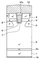
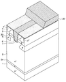
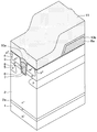
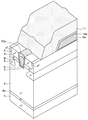
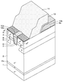
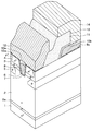
- FIG. 1 is a cross-sectional view of a semiconductor device according to a first embodiment.
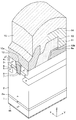
- FIG. 2 is a perspective sectional view of the semiconductor device shown in FIG.
- FIG. 7 is a cross-sectional view showing the manufacturing process of the semiconductor device shown in FIG. 1;
- 3C is a cross-sectional view showing the manufacturing process of the semiconductor device continued from FIG. 3A;
- FIG. 3C is a cross-sectional view showing the manufacturing process of the semiconductor device, following FIG. 3B;
- FIG. 3C is a cross-sectional view showing the manufacturing process of the semiconductor device, following FIG. 3C;
- FIG. 3D is a cross-sectional view showing the manufacturing process of the semiconductor device, following FIG. 3D;
- FIG. 3D is a cross-sectional view showing the manufacturing process of the semiconductor device, following FIG. 3D;
- FIG. 3E is a cross-sectional view showing the manufacturing process of the semiconductor device, following FIG. 3E;
- 3F is a cross-sectional view showing the manufacturing process of the semiconductor device, following FIG. 3F;
- FIG. 3G is a cross-sectional view showing the manufacturing process of the semiconductor device, following FIG. 3G;
- 3J is a cross-sectional view showing the manufacturing process of the semiconductor device, following FIG. 3H;
- FIG. 3E is a cross-sectional view showing the manufacturing process of the semiconductor device, following FIG. 3E;
- 3F is a cross-sectional view showing the manufacturing process of the semiconductor device, following FIG. 3F;
- 3G is a cross-sectional view showing the manufacturing process of the semiconductor device, following FIG. 3G;
- 3J is a cross-sectional view showing the manufacturing process of the semiconductor device, following FIG. 3H;
- FIG. 3H is a cross-sectional view showing the manufacturing process of the semiconductor device, following FIG. 3H;
- the semiconductor device according to the present embodiment is, as shown in FIGS. 1 and 2, formed with a vertical MOSFET as a semiconductor element having a MOS structure.
- the vertical MOSFET is formed in the cell region of the semiconductor device, and the outer peripheral breakdown voltage structure is formed so as to surround the cell region, but the semiconductor device is configured here. Only the gate lead-out portion in the MOSFET is shown.
- the horizontal direction in FIG. 1 and the X direction in FIG. 2 are taken as the width direction
- the vertical direction in FIG. 1 and the Y direction in FIG. 2 as the depth direction
- the Z direction in FIG. 2 will be described as the thickness direction or the depth direction.
- an n + -type substrate 1 made of SiC is used as a semiconductor substrate.
- the depth direction is made to coincide with the off direction.
- an off substrate having a (0001) Si surface and a predetermined off angle is used, and for example, the off direction is set to ⁇ 11-20>.
- the n-type impurity concentration of the n + -type substrate 1 is, eg, 1.0 ⁇ 10 19 / cm 3 .
- n -- type drift layer 2 made of SiC, p-type base region 3 and n + -type source region 4 are epitaxially grown in order.
- the n ⁇ -type drift layer 2 has, for example, an n-type impurity concentration of 0.5 to 2.0 ⁇ 10 16 / cm 3 and a thickness of 5 to 14 ⁇ m.
- n - the boundary between the n + -type substrate 1 of the type drift layer 2, optionally n - even each other by the type drift layer 2 to form a partially high concentration and buffer layer 2a good.
- the p-type base region 3 is a portion where the channel region is formed, and the p-type impurity concentration is, for example, about 2.0 ⁇ 10 17 / cm 3 and the thickness is 0.5 to 2 ⁇ m. Further, in the case of the present embodiment, the surface layer portion of the p-type base region 3 is a contact region in which the p-type impurity concentration is increased.
- the n + -type source region 4 has a higher impurity concentration than the n ⁇ -type drift layer 2 and has an n-type impurity concentration of, for example, 2.5 ⁇ 10 18 to 1.0 ⁇ 10 19 / cm 3 in the surface layer portion. It is composed of about 0.5 to 2 ⁇ m.
- a p-type deep layer 5 is formed in the surface layer portion of the n ⁇ -type drift layer 2, that is, below the p-type base region 3.
- the p-type deep layer 5 has a p-type impurity concentration higher than that of the p-type base region 3, and a plurality of the p-type deep layers 5 are arranged at equal intervals and separated from each other without intersecting each other. It is done.
- each p-type deep layer 5 has a p-type impurity concentration of 1.0 ⁇ 10 17 to 1.0 ⁇ 10 19 / cm 3 and a width of 0.7 ⁇ m.
- Each p-type deep layer 5 has a depth of 0.4 ⁇ m or more, and is formed to a position deeper than the trench gate structure described later, thereby suppressing entry of an electric field into the trench gate structure.
- the p-type deep layer 5 is formed only in the surface layer portion of the n ⁇ -type drift layer 2, but the n ⁇ -type source region 4 and the p-type base region 3 are penetrated to form the n ⁇ -type It may be formed to reach the drift layer 2.
- a trench can be formed from the surface of the n + -type source region 4 and the p-type deep layer 5 can be formed to be embedded in the trench.
- the width is 0.8 ⁇ m and the depth is p-type base region 3 and n + -type source region so as to penetrate p-type base region 3 and n + -type source region 4 to reach n ⁇ -type drift layer 2.
- a gate trench 6 which is 0.2 to 0.4 ⁇ m deeper than the total film thickness of 4 is formed.
- the p-type base region 3 and the n + -type source region 4 described above are arranged in contact with the side surfaces of the gate trench 6.
- the gate trench 6 is formed in a linear layout in which the width direction, the depth direction, and the thickness direction of the vertical MOSFET are respectively the width direction, the longitudinal direction, and the depth direction. Further, although only one is shown in FIGS. 1 and 2, a plurality of gate trenches 6 are arranged at equal intervals in the lateral direction of the paper surface of FIG. It is arranged in the form of stripes.
- a portion of the p-type base region 3 located on the side surface of the gate trench 6 is a channel region connecting the n + -type source region 4 and the n ⁇ -type drift layer 2 when the vertical MOSFET operates.
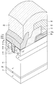
- a gate insulating film 7 is formed on the inner wall surface of the gate trench 6 including the channel region.
- a gate electrode 8 made of doped polysilicon is formed on the surface of the gate insulating film 7, and the inside of the gate trench 6 is buried with the gate insulating film 7 and the gate electrode 8.
- the gate insulating film 7 may be formed to the outside of the gate trench 6 but is preferably formed only in the gate trench 6.
- a thermal oxide film 10 a corresponding to a first interlayer insulating film formed by thermally oxidizing the surface of the gate electrode 8 is provided on the gate electrode 8.
- the thermal oxide film 10a is formed of a silicon oxide film formed by thermal oxidation, and contains therein an impurity serving as a dopant for the semiconductor. This impurity is the same as that contained in the gate electrode 8 and is, for example, phosphorus (P) or boron (B).
- the thermal oxide film 10a may contain either or both of phosphorus and boron as impurities.
- the thermal oxide film 10 a is formed in the gate trench 6 and is thicker than the portion on the inner wall surface of the gate trench 6 where the channel region is formed in the gate insulating film 7 and thinner than 500 nm. .
- insulation separation between the gate electrode 8 and the source electrode 12 described later can be surely performed.
- is made thinner than 500nm thermal oxide film 10a it can as a gate electrode 8 is accurately positioned on the opposite side to the n + -type source region 4 across the gate insulating film 7, n + -type source region It is not necessary to form 4 to a position deeper than necessary.
- thermal oxide film 10 a has a height of ⁇ 100 nm with respect to the surface of the n + -type source region 4 outside the gate trench 6.
- thermal oxide film 10a has a surface which is at the same height with respect to the surface of n + -type source region 4, or in the inside of gate trench 6 beyond that, or a gate trench further than that. It is in the state of protruding to the outside of 6. Then, if the surface of thermal oxide film 10 a is in a state in which gate trench 6 is inward of the surface of n + type source region 4, the amount of intrusion is 100 nm or less, and protrudes outside gate trench 6. If there is, the protrusion amount is 100 nm or less.
- thermal oxide film 10a As for the height of thermal oxide film 10a, the state in which the surface of thermal oxide film 10a is in the inside of gate trench 6 and the state in which it protrudes outward from the surface of n + type source region 4 are minus and plus, respectively. Is represented by.
- the thermal oxide film 10 a does not extend outside the gate trench 6 in the width direction of the gate trench 6, and is terminated at the inside of the gate trench 6 in the width direction. Therefore, the contact regions of the n + -type source region 4 and the p-type base region 3 are exposed from the thermal oxide film 10 a.
- a plurality of trench gate structures are arranged in a stripe shape.
- the gate electrode 8 is configured so as to connect the ends in the longitudinal direction of the respective trench gate structures, or to connect the intermediate positions in the longitudinal direction of the respective trench gate structures although not shown.
- a gate lead-out portion 8a in which doped polysilicon is left is formed.
- the gate lead-out portion 8 a is formed to protrude above the gate electrode 8, that is, from the SiC surface such as the n + -type source region 4.
- the thermal oxide film 10b is partially disposed on the gate lead-out portion 8a, and the thermal oxide film 10b is formed above the SiC surface such as the n + -type source region 4 in this portion. It has become.
- An interlayer insulating film 11 corresponding to the interlayer insulating film is formed.
- the interlayer insulating film 11 is formed of, for example, BPSG.
- the thickness of the interlayer insulating film 11 is, eg, 600 nm.
- Interlayer insulating film 11 is removed at a position other than on or in the vicinity of gate lead-out portion 8a in the cell region where the vertical MOSFET is formed. Therefore, the gate insulating film 7, the thermal oxide film 10a, the contact region of the p-type base region 3 and the n + -type source region 4 are exposed from the interlayer insulating film 11 at positions other than the gate lead-out portion 8a.
- the source electrode 12 is formed at this exposed position, and is electrically connected to the contact region of the p-type base region 3 and the n + -type source region 4.
- interlayer insulating film 11 is partially removed also on gate lead-out portion 8a.
- the thermal oxide film 10 b is also removed, and the contact hole 13 is formed.
- the gate wiring layer 14 is formed at the position where the contact hole 13 is formed, whereby the gate lead-out portion 8 a is connected.
- the source electrode 12 and the gate wiring layer 14 are made of a plurality of metals such as Ni / Al. Then, at least a portion of the plurality of metals in contact with the n-type SiC, specifically the n + -type source region 4 and the like, is made of a metal that can make an ohmic contact with the n-type SiC. Further, at least a portion of the plurality of metals in contact with the p-type SiC, specifically, the p-type deep layer 5, and the like are made of a metal capable of being in ohmic contact with the p-type SiC. The source electrode 12 and the gate wiring layer 14 are arranged separately from each other, and are electrically insulated by the thermal oxide films 10 a and 10 b and the interlayer insulating film 11.
- the surfaces of the source electrode 12, the gate wiring layer 14 and the interlayer insulating film 11 are covered and protected by a passivation film 15. Then, although not shown, the source electrode 12 and the gate wiring layer 14 are exposed by partially removing the passivation film 15, and are connected to the source pad and the gate pad for external connection.
- n + -type substrate 1 On the back side of the n + -type substrate 1 n + -type substrate 1 and electrically connected to the drain electrode 16 are formed.
- Such a structure constitutes an n-channel type inverted trench gate vertical MOSFET.
- a cell region is configured by arranging a plurality of such vertical MOSFETs in a plurality of cells.
- a semiconductor device is configured by configuring an outer peripheral withstand voltage structure such as a guard ring (not shown) so as to surround a cell region in which such a vertical MOSFET is formed.
- the SiC semiconductor device having the vertical MOSFET configured in this way has a gate voltage Vg of 20 V with respect to the gate electrode 8 in a state where the source voltage Vs is 0 V and the drain voltage Vd is 1 to 1.5 V, for example. It is made to operate by applying. That is, when the gate voltage Vg is applied to the vertical MOSFET, a channel region is formed in the p-type base region 3 in a portion in contact with the gate trench 6, and a current flows between the drain and the source.
- the thermal oxide film 10a is disposed in the gate trench 6. Therefore, it is possible to secure insulation isolation between the gate and the source by the thermal oxide film 10a. Further, while the thermal oxide film 10 a is disposed in the gate trench 6, the thermal oxide film 10 a is configured not to protrude from the gate trench 6 in the width direction of the gate trench 6. Thus, the source electrode 12 is properly brought into contact with the contact region of the p-type base region 3 and the n + -type source region 4. Therefore, the contact of the source electrode 12 can be properly performed.
- the thermal oxide film 10a does not project into the shape of the surface of the SiC, or even if it protrudes, the amount of projection is small. Therefore, it is possible to suppress the occurrence of the crack in the thermal oxide film 10a due to the stress accompanying the temperature change and the like, and it becomes possible to suppress the occurrence of the gate-source leak.
- n + -type substrate 1 is prepared as a semiconductor substrate.
- an n ⁇ -type drift layer 2 made of SiC is formed on the main surface of the n + -type substrate 1 using a chemical vapor deposition (hereinafter referred to as CVD) apparatus or the like.
- CVD chemical vapor deposition
- a buffer layer 2a in which the n ⁇ -type drift layer 2 has a partially high concentration may be formed.
- the p-type deep layer 5 is formed by ion-implanting p-type impurities.
- the mask is removed, and the p-type base region 3 and the n + -type source region 4 are formed on the n ⁇ -type drift layer 2 on which the p-type deep layer 5 is formed.
- the n + -type source region 4 is formed by ion implantation of an n-type impurity.
- the contact region of the p-type base region 3 is formed by ion implantation of a p-type impurity.
- a mask (not shown) is disposed on the surfaces of p type base region 3 and n + type source region 4 to open a region for forming a trench gate structure of the mask.
- the gate trench 6 is formed by performing anisotropic etching such as RIE (Reactive Ion Etching) using a mask. For example, etching is performed with a setting such that the depth of the gate trench 6 is 0.2 to 0.4 ⁇ m deeper than the total film thickness of the p-type base region 3 and the n + -type source region 4.
- RIE Reactive Ion Etching
- the gate insulating film 7 is formed, for example, by thermal oxidation, and the gate insulating film 7 covers the inner wall surface of the gate trench 6 and the surface of the n + -type source region 4.
- polysilicon 20 doped with, for example, an n-type impurity is deposited to form gate electrode 8 and gate lead-out portion 8a, and then this is etched back.
- a mask is disposed so as to cover a portion to be the gate lead-out portion 8a, and the polysilicon 20 is etched back.
- the polysilicon 20 is left in the gate trench 6, and the polysilicon 20 is left to project above the SiC surface at the planned formation position of the gate lead-out portion 8a.
- the polysilicon 20 is removed except in the gate trench 6 and the planned formation position of the gate lead-out portion 8a. Thereafter, the mask used at the time of etch back is removed.
- Step shown in FIG. 3D By heat treatment, the surface of the polysilicon 20 is thermally oxidized.
- the heat treatment is performed, for example, by wet oxidation at 1050 ° C. for 30 minutes.
- the thermal oxidation film 10 a is formed in the gate trench 6 by thermally oxidizing the polysilicon 20, and the remaining polysilicon 20 forms the gate electrode 8.
- the thermal oxide film 10b is also formed on the surface of the polysilicon 20 at the planned formation position of the gate lead-out portion 8a, and the remaining polysilicon 20 forms the gate lead-out portion 8a.
- the thickness of the thermal oxide films 10a and 10b is arbitrary, but the height of the thermal oxide film 10a with respect to the surface of the n + -type source region 4 outside the gate trench 6 after etch back in the step shown in FIG. Is set to be ⁇ 100 nm.
- thermal oxide films 10a and 10b can be formed.
- the thermal oxide films 10a and 10b formed in this manner are those obtained by thermally oxidizing the impurity-doped polysilicon 20, and thus include the impurity serving as the dopant for the semiconductor as the impurity. .
- the thermal oxide films 10a and 10b are higher in height than the polysilicon 20 before thermal oxidation due to volume expansion.
- the heat treatment is performed at a temperature at which the polysilicon 20 is thermally oxidized but the SiC is hardly oxidized. By doing this, the thermal oxide films 10a and 10b are formed while the thickness of the gate insulating film 7 is hardly increased.
- Step shown in FIG. 3E After depositing the interlayer insulating film 11 made of BPSG or the like on the surface of the thermal oxide films 10a and 10b and the gate insulating film 7 using a CVD apparatus or the like, reflow processing is performed.
- the film thickness of the interlayer insulating film 11 at this time is arbitrary, but is thicker than the thermal oxide films 10a and 10b.
- Step shown in FIG. 3F After arranging a mask (not shown) covering a portion corresponding to gate lead-out portion 8a of interlayer insulating film 11, a portion of interlayer insulating film 11 or gate insulating film 7 located outside gate trench 6 and a thermal oxide film Etch back the portion of 10 a that protrudes from the gate trench 6. Specifically, etch back is performed by chemical dry etching (hereinafter referred to as CDE).
- CDE chemical dry etching
- the etching rate at the time of etching back is that of the thermal oxide film 10a. Is slower than the interlayer insulating film 11. That is, the interlayer insulating film 11 is easily etched, and the thermal oxide film 10a can be etched back under the condition that etching is difficult.
- the thermal oxide film 10a is not so etched, which is preferable.
- chemical dry etching is used as chemical etching here, wet etching may be used.
- interlayer insulating film 11 can be completely removed while leaving thermal oxide film 10 a in gate trench 6.
- the gate insulating film 7 formed thinner than the thermal oxide film 10a is also completely or almost completely removed from the portion located outside the gate trench 6, and the n + -type source region 4 and the p-type are formed.
- the contact area of base area 3 is exposed.
- the thermal oxide film 10a functioning as an interlayer insulating film for insulating between the gate and the source remains in the gate trench 6 in a self-aligned manner and is not formed outside the gate trench 6 in the width direction. it can.
- a metal layer 12a for contact made of, for example, Ni is formed. Thereafter, heat treatment is performed as necessary.
- a Ni silicide layer can be formed.
- the planned formation position of the contact hole 13 in the mask is opened, and the interlayer insulating film 11 and the thermal oxide film 10 b are etched to form the contact hole 13.
- a metal layer is formed on the metal layer 12 a and the interlayer insulating film 11 including the inside of the contact hole 13 and patterned to form the source electrode 12 and the gate wiring layer 14.
- a passivation film 15 is formed to cover the source electrode 12 and the gate wiring layer 14 and then patterned to expose desired portions of the source electrode 12 and the gate wiring layer 14.
- insulation between the gate electrode 8 and the source electrode 12 can be performed by the thermal oxide film 10 a configured by thermally oxidizing a part of the gate electrode 8.
- the thermal oxide film 10a configured by thermally oxidizing a part of the gate electrode 8 does not have a shape protruding so much from the SiC surface, it is difficult for a crack due to a stress caused by a temperature change or the like. Therefore, it is possible to secure gate-source insulation isolation.
- the interlayer insulating film 11 is removed from above the contact regions of the n + -type source region 4 and the p-type base region 3 by etch back. Therefore, the source electrode 12 can be properly contacted on both sides of the gate electrode 8.
- the thermal oxide film 10a functioning as an interlayer insulating film for insulating between the gate and the source remains in the gate trench 6 in a self-aligned manner, and can not be formed outside the gate trench 6 in the width direction. Therefore, mass productivity of the SiC semiconductor device can be secured.
- the n-channel vertical MOSFET having the first conductivity type as n-type and the second conductivity type as p-type has been described as an example, but the conductivity type of each component is inverted. It may be a vertical p-channel type MOSFET.
- the vertical MOSFET is described as an example of the semiconductor element having the MOS structure.
- the present disclosure can be applied to an IGBT having a similar MOS structure.
- the conductivity type of the n + -type substrate 1 is merely changed from n-type to p-type in each of the above embodiments, and the other structure and manufacturing method are the same as in the above embodiments. It is.
- a bar (-) should normally be added above the desired number, but since there is a limitation in expression based on the electronic application, it is desirable in the present specification to be a desired one. A bar shall be put in front of the numbers.
Landscapes
- Engineering & Computer Science (AREA)
- Physics & Mathematics (AREA)
- Condensed Matter Physics & Semiconductors (AREA)
- General Physics & Mathematics (AREA)
- Manufacturing & Machinery (AREA)
- Computer Hardware Design (AREA)
- Microelectronics & Electronic Packaging (AREA)
- Power Engineering (AREA)
- Electrodes Of Semiconductors (AREA)
- Formation Of Insulating Films (AREA)
Priority Applications (2)
| Application Number | Priority Date | Filing Date | Title |
|---|---|---|---|
| CN201880061858.5A CN111149214B (zh) | 2017-09-27 | 2018-09-20 | 碳化硅半导体装置 |
| US16/804,565 US11171231B2 (en) | 2017-09-27 | 2020-02-28 | Silicon carbide semiconductor device and method for manufacturing the same |
Applications Claiming Priority (2)
| Application Number | Priority Date | Filing Date | Title |
|---|---|---|---|
| JP2017-186917 | 2017-09-27 | ||
| JP2017186917A JP6750590B2 (ja) | 2017-09-27 | 2017-09-27 | 炭化珪素半導体装置 |
Related Child Applications (1)
| Application Number | Title | Priority Date | Filing Date |
|---|---|---|---|
| US16/804,565 Continuation US11171231B2 (en) | 2017-09-27 | 2020-02-28 | Silicon carbide semiconductor device and method for manufacturing the same |
Publications (1)
| Publication Number | Publication Date |
|---|---|
| WO2019065462A1 true WO2019065462A1 (ja) | 2019-04-04 |
Family
ID=65903712
Family Applications (1)
| Application Number | Title | Priority Date | Filing Date |
|---|---|---|---|
| PCT/JP2018/034870 Ceased WO2019065462A1 (ja) | 2017-09-27 | 2018-09-20 | 炭化珪素半導体装置 |
Country Status (4)
| Country | Link |
|---|---|
| US (1) | US11171231B2 (enExample) |
| JP (1) | JP6750590B2 (enExample) |
| CN (1) | CN111149214B (enExample) |
| WO (1) | WO2019065462A1 (enExample) |
Cited By (2)
| Publication number | Priority date | Publication date | Assignee | Title |
|---|---|---|---|---|
| US20230009078A1 (en) * | 2021-07-06 | 2023-01-12 | Denso Corporation | Method of manufacturing silicon carbide semiconductor device |
| WO2025134220A1 (ja) * | 2023-12-19 | 2025-06-26 | 三菱電機株式会社 | 半導体装置、および、半導体装置の製造方法 |
Families Citing this family (5)
| Publication number | Priority date | Publication date | Assignee | Title |
|---|---|---|---|---|
| JP6981890B2 (ja) * | 2018-01-29 | 2021-12-17 | ルネサスエレクトロニクス株式会社 | 半導体装置 |
| US11004940B1 (en) * | 2020-07-31 | 2021-05-11 | Genesic Semiconductor Inc. | Manufacture of power devices having increased cross over current |
| JP7540334B2 (ja) * | 2020-12-25 | 2024-08-27 | 株式会社デンソー | 半導体装置の製造方法 |
| JP7513565B2 (ja) * | 2021-04-14 | 2024-07-09 | 株式会社デンソー | スイッチング素子の製造方法 |
| CN114695556A (zh) * | 2022-03-30 | 2022-07-01 | 南京芯长征科技有限公司 | 高可靠性SiC沟槽型功率半导体器件及制备方法 |
Citations (5)
| Publication number | Priority date | Publication date | Assignee | Title |
|---|---|---|---|---|
| JPH09129877A (ja) * | 1995-10-30 | 1997-05-16 | Toyota Central Res & Dev Lab Inc | 半導体装置の製造方法、絶縁ゲート型半導体装置の製造方法および絶縁ゲート型半導体装置 |
| JP2007150142A (ja) * | 2005-11-30 | 2007-06-14 | Toshiba Corp | 半導体装置 |
| WO2009122486A1 (ja) * | 2008-03-31 | 2009-10-08 | 三菱電機株式会社 | 半導体装置 |
| WO2012144271A1 (ja) * | 2011-04-19 | 2012-10-26 | 日産自動車株式会社 | 半導体装置およびその製造方法 |
| JP2016119392A (ja) * | 2014-12-22 | 2016-06-30 | 日産自動車株式会社 | 絶縁ゲート型半導体装置及びその製造方法 |
Family Cites Families (8)
| Publication number | Priority date | Publication date | Assignee | Title |
|---|---|---|---|---|
| JP4096569B2 (ja) * | 2002-01-31 | 2008-06-04 | 株式会社デンソー | 炭化珪素半導体装置とその製造方法 |
| JP2008098593A (ja) * | 2006-09-15 | 2008-04-24 | Ricoh Co Ltd | 半導体装置及びその製造方法 |
| EP2091083A3 (en) * | 2008-02-13 | 2009-10-14 | Denso Corporation | Silicon carbide semiconductor device including a deep layer |
| JP5588670B2 (ja) * | 2008-12-25 | 2014-09-10 | ローム株式会社 | 半導体装置 |
| JP2013105841A (ja) | 2011-11-11 | 2013-05-30 | Toshiba Corp | 半導体装置とその製造方法 |
| JP5884617B2 (ja) * | 2012-04-19 | 2016-03-15 | 株式会社デンソー | 炭化珪素半導体装置およびその製造方法 |
| JPWO2014054121A1 (ja) * | 2012-10-02 | 2016-08-25 | 三菱電機株式会社 | 半導体装置 |
| JP6354525B2 (ja) * | 2014-11-06 | 2018-07-11 | 株式会社デンソー | 炭化珪素半導体装置の製造方法 |
-
2017
- 2017-09-27 JP JP2017186917A patent/JP6750590B2/ja active Active
-
2018
- 2018-09-20 WO PCT/JP2018/034870 patent/WO2019065462A1/ja not_active Ceased
- 2018-09-20 CN CN201880061858.5A patent/CN111149214B/zh active Active
-
2020
- 2020-02-28 US US16/804,565 patent/US11171231B2/en active Active
Patent Citations (5)
| Publication number | Priority date | Publication date | Assignee | Title |
|---|---|---|---|---|
| JPH09129877A (ja) * | 1995-10-30 | 1997-05-16 | Toyota Central Res & Dev Lab Inc | 半導体装置の製造方法、絶縁ゲート型半導体装置の製造方法および絶縁ゲート型半導体装置 |
| JP2007150142A (ja) * | 2005-11-30 | 2007-06-14 | Toshiba Corp | 半導体装置 |
| WO2009122486A1 (ja) * | 2008-03-31 | 2009-10-08 | 三菱電機株式会社 | 半導体装置 |
| WO2012144271A1 (ja) * | 2011-04-19 | 2012-10-26 | 日産自動車株式会社 | 半導体装置およびその製造方法 |
| JP2016119392A (ja) * | 2014-12-22 | 2016-06-30 | 日産自動車株式会社 | 絶縁ゲート型半導体装置及びその製造方法 |
Cited By (2)
| Publication number | Priority date | Publication date | Assignee | Title |
|---|---|---|---|---|
| US20230009078A1 (en) * | 2021-07-06 | 2023-01-12 | Denso Corporation | Method of manufacturing silicon carbide semiconductor device |
| WO2025134220A1 (ja) * | 2023-12-19 | 2025-06-26 | 三菱電機株式会社 | 半導体装置、および、半導体装置の製造方法 |
Also Published As
| Publication number | Publication date |
|---|---|
| US20200203526A1 (en) | 2020-06-25 |
| CN111149214A (zh) | 2020-05-12 |
| CN111149214B (zh) | 2023-11-03 |
| JP6750590B2 (ja) | 2020-09-02 |
| US11171231B2 (en) | 2021-11-09 |
| JP2019062126A (ja) | 2019-04-18 |
Similar Documents
| Publication | Publication Date | Title |
|---|---|---|
| US11171231B2 (en) | Silicon carbide semiconductor device and method for manufacturing the same | |
| EP2755237B1 (en) | Trench MOS gate semiconductor device and method of fabricating the same | |
| JP6354525B2 (ja) | 炭化珪素半導体装置の製造方法 | |
| CN102403338B (zh) | SiC半导体器件及其制造方法 | |
| CN105304692B (zh) | 用于在沟槽功率mosfet中优化端接设计的不对称多晶硅栅极的制备方法 | |
| JP4577355B2 (ja) | 炭化珪素半導体装置およびその製造方法 | |
| JP5772842B2 (ja) | 炭化珪素半導体装置 | |
| JPH11103056A (ja) | 横型mos素子を含む半導体装置 | |
| CN210296383U (zh) | Mosfet器件和碳化硅mosfet器件 | |
| TW201801311A (zh) | 溝槽式功率半導體元件 | |
| JP2010045130A (ja) | 半導体装置および半導体装置の製造方法 | |
| TW201820469A (zh) | 複合屏蔽自對準的溝槽mosfet及其製備方法 | |
| US9178055B2 (en) | Semiconductor device | |
| US10141415B2 (en) | Combined gate and source trench formation and related structure | |
| TW201828478A (zh) | 半導體裝置及其製造方法 | |
| JP5616720B2 (ja) | 半導体装置およびその製造方法 | |
| CN113964038A (zh) | 沟槽栅mosfet器件的制造方法 | |
| KR101469343B1 (ko) | 수직 파워 mosfet 및 그 제조 방법 | |
| US7494876B1 (en) | Trench-gated MIS device having thick polysilicon insulation layer at trench bottom and method of fabricating the same | |
| US20160211349A1 (en) | Semiconductor device and a method for manufacturing a semiconductor device | |
| TWI588991B (zh) | 溝槽式功率半導體元件 | |
| TWI574405B (zh) | Silicon carbide semiconductor device, method for manufacturing silicon carbide semiconductor device, and design method of silicon carbide semiconductor device | |
| JP2008084901A (ja) | 半導体装置およびその製造方法 | |
| JP2012199468A (ja) | 半導体装置の製造方法 | |
| JP4623656B2 (ja) | 縦型ゲート半導体装置およびその製造方法 |
Legal Events
| Date | Code | Title | Description |
|---|---|---|---|
| 121 | Ep: the epo has been informed by wipo that ep was designated in this application |
Ref document number: 18863447 Country of ref document: EP Kind code of ref document: A1 |
|
| NENP | Non-entry into the national phase |
Ref country code: DE |
|
| 122 | Ep: pct application non-entry in european phase |
Ref document number: 18863447 Country of ref document: EP Kind code of ref document: A1 |