WO2019013000A1 - 端子及び端子付き基板 - Google Patents
端子及び端子付き基板 Download PDFInfo
- Publication number
- WO2019013000A1 WO2019013000A1 PCT/JP2018/024519 JP2018024519W WO2019013000A1 WO 2019013000 A1 WO2019013000 A1 WO 2019013000A1 JP 2018024519 W JP2018024519 W JP 2018024519W WO 2019013000 A1 WO2019013000 A1 WO 2019013000A1
- Authority
- WO
- WIPO (PCT)
- Prior art keywords
- terminal
- substrate
- plate
- projecting
- wall
- Prior art date
- Legal status (The legal status is an assumption and is not a legal conclusion. Google has not performed a legal analysis and makes no representation as to the accuracy of the status listed.)
- Ceased
Links
Images





Classifications
-
- H—ELECTRICITY
- H01—ELECTRIC ELEMENTS
- H01R—ELECTRICALLY-CONDUCTIVE CONNECTIONS; STRUCTURAL ASSOCIATIONS OF A PLURALITY OF MUTUALLY-INSULATED ELECTRICAL CONNECTING ELEMENTS; COUPLING DEVICES; CURRENT COLLECTORS
- H01R12/00—Structural associations of a plurality of mutually-insulated electrical connecting elements, specially adapted for printed circuits, e.g. printed circuit boards [PCB], flat or ribbon cables, or like generally planar structures, e.g. terminal strips, terminal blocks; Coupling devices specially adapted for printed circuits, flat or ribbon cables, or like generally planar structures; Terminals specially adapted for contact with, or insertion into, printed circuits, flat or ribbon cables, or like generally planar structures
- H01R12/50—Fixed connections
- H01R12/51—Fixed connections for rigid printed circuits or like structures
- H01R12/55—Fixed connections for rigid printed circuits or like structures characterised by the terminals
- H01R12/58—Fixed connections for rigid printed circuits or like structures characterised by the terminals terminals for insertion into holes
-
- H—ELECTRICITY
- H01—ELECTRIC ELEMENTS
- H01R—ELECTRICALLY-CONDUCTIVE CONNECTIONS; STRUCTURAL ASSOCIATIONS OF A PLURALITY OF MUTUALLY-INSULATED ELECTRICAL CONNECTING ELEMENTS; COUPLING DEVICES; CURRENT COLLECTORS
- H01R4/00—Electrically-conductive connections between two or more conductive members in direct contact, i.e. touching one another; Means for effecting or maintaining such contact; Electrically-conductive connections having two or more spaced connecting locations for conductors and using contact members penetrating insulation
- H01R4/02—Soldered or welded connections
- H01R4/027—Soldered or welded connections comprising means for positioning or holding the parts to be soldered or welded
-
- H—ELECTRICITY
- H01—ELECTRIC ELEMENTS
- H01R—ELECTRICALLY-CONDUCTIVE CONNECTIONS; STRUCTURAL ASSOCIATIONS OF A PLURALITY OF MUTUALLY-INSULATED ELECTRICAL CONNECTING ELEMENTS; COUPLING DEVICES; CURRENT COLLECTORS
- H01R12/00—Structural associations of a plurality of mutually-insulated electrical connecting elements, specially adapted for printed circuits, e.g. printed circuit boards [PCB], flat or ribbon cables, or like generally planar structures, e.g. terminal strips, terminal blocks; Coupling devices specially adapted for printed circuits, flat or ribbon cables, or like generally planar structures; Terminals specially adapted for contact with, or insertion into, printed circuits, flat or ribbon cables, or like generally planar structures
- H01R12/50—Fixed connections
- H01R12/51—Fixed connections for rigid printed circuits or like structures
- H01R12/55—Fixed connections for rigid printed circuits or like structures characterised by the terminals
- H01R12/57—Fixed connections for rigid printed circuits or like structures characterised by the terminals surface mounting terminals
-
- H—ELECTRICITY
- H01—ELECTRIC ELEMENTS
- H01R—ELECTRICALLY-CONDUCTIVE CONNECTIONS; STRUCTURAL ASSOCIATIONS OF A PLURALITY OF MUTUALLY-INSULATED ELECTRICAL CONNECTING ELEMENTS; COUPLING DEVICES; CURRENT COLLECTORS
- H01R12/00—Structural associations of a plurality of mutually-insulated electrical connecting elements, specially adapted for printed circuits, e.g. printed circuit boards [PCB], flat or ribbon cables, or like generally planar structures, e.g. terminal strips, terminal blocks; Coupling devices specially adapted for printed circuits, flat or ribbon cables, or like generally planar structures; Terminals specially adapted for contact with, or insertion into, printed circuits, flat or ribbon cables, or like generally planar structures
- H01R12/50—Fixed connections
- H01R12/59—Fixed connections for flexible printed circuits, flat or ribbon cables or like structures
- H01R12/65—Fixed connections for flexible printed circuits, flat or ribbon cables or like structures characterised by the terminal
-
- H—ELECTRICITY
- H01—ELECTRIC ELEMENTS
- H01R—ELECTRICALLY-CONDUCTIVE CONNECTIONS; STRUCTURAL ASSOCIATIONS OF A PLURALITY OF MUTUALLY-INSULATED ELECTRICAL CONNECTING ELEMENTS; COUPLING DEVICES; CURRENT COLLECTORS
- H01R13/00—Details of coupling devices of the kinds covered by groups H01R12/70 or H01R24/00 - H01R33/00
- H01R13/40—Securing contact members in or to a base or case; Insulating of contact members
- H01R13/42—Securing in a demountable manner
- H01R13/422—Securing in resilient one-piece base or case, e.g. by friction; One-piece base or case formed with resilient locking means
- H01R13/4223—Securing in resilient one-piece base or case, e.g. by friction; One-piece base or case formed with resilient locking means comprising integral flexible contact retaining fingers
-
- H—ELECTRICITY
- H01—ELECTRIC ELEMENTS
- H01R—ELECTRICALLY-CONDUCTIVE CONNECTIONS; STRUCTURAL ASSOCIATIONS OF A PLURALITY OF MUTUALLY-INSULATED ELECTRICAL CONNECTING ELEMENTS; COUPLING DEVICES; CURRENT COLLECTORS
- H01R4/00—Electrically-conductive connections between two or more conductive members in direct contact, i.e. touching one another; Means for effecting or maintaining such contact; Electrically-conductive connections having two or more spaced connecting locations for conductors and using contact members penetrating insulation
- H01R4/02—Soldered or welded connections
- H01R4/028—Soldered or welded connections comprising means for preventing flowing or wicking of solder or flux in parts not desired
-
- H—ELECTRICITY
- H01—ELECTRIC ELEMENTS
- H01R—ELECTRICALLY-CONDUCTIVE CONNECTIONS; STRUCTURAL ASSOCIATIONS OF A PLURALITY OF MUTUALLY-INSULATED ELECTRICAL CONNECTING ELEMENTS; COUPLING DEVICES; CURRENT COLLECTORS
- H01R13/00—Details of coupling devices of the kinds covered by groups H01R12/70 or H01R24/00 - H01R33/00
- H01R13/02—Contact members
- H01R13/10—Sockets for co-operation with pins or blades
Definitions
- Patent Document 1 describes a connector in which a plurality of plug terminals are fixed to a plug insulator, and the plurality of plug terminals extended from the back surface of the plug insulator have offset bent end portions of the circuit board. It is soldered to the connection electrode on the surface.
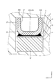
- the terminals to be soldered to the substrate are generally formed by plating a metal plate material and then punching it with a press. Therefore, as shown in FIG. 9, the plated layers 2A and 2B are formed on the upper and lower plate surfaces of the terminal 1, but the plated layers are formed on the left and right of the terminal 1 to be cut end faces 3A and 3B by a press machine. Is not formed.
- the copper foil 6 can be soldered to the lower surface of the terminal 1 on which the plating layer 2B is formed.
- the solder 7 does not spread on the left and right cut end surfaces 3A and 3B of the terminal 1 where the plating layer is not formed, there is a concern that the strength of the soldering may be reduced.
- the technology described in the present specification is completed based on the above-mentioned circumstances, and it is an object of the present invention to suppress a decrease in soldering strength of a terminal soldered to a substrate.
- the terminal described in the present specification is a terminal having a terminal connection portion connected to a mating terminal and a substrate connection portion connected to the conductive path of the substrate, and the substrate connection portion is the terminal connection portion.
- a plate-like plate-like portion disposed behind the plate and soldered to the conductive path of the substrate, and a plate-like member bent from an edge portion on the side of the plate-like portion and protruding to the side opposite to the substrate side And a plating layer is formed on the plate surface of the plate-like portion and the first protrusion wall.
- the conductive path of the substrate is soldered to the plate-like portion, and the first projecting wall is bent from the side edge of the plate-like portion and protrudes to the side opposite to the substrate.
- the solder for connecting the plate-like portion and the conductive path of the substrate can be spread on the bent portion where the plated layer on the base end side of the first projecting wall is formed and bent, so the side edge portion of the plate-like portion It is possible to suppress a decrease in soldering strength as compared to the configuration described above.
- the terminal connection portion extends in a direction intersecting with the plate surface of the plate-like portion, and has a pair of side walls disposed opposite to each other, and the counterpart terminal is configured to be inserted between the pair of side walls.
- the outer surface of the first projecting wall is disposed in the same plane as the outer surface of the side wall or inside the same plane. In this way, for example, when the terminal is inserted into the cavity of the connector housing, the first projecting wall is unlikely to be an obstacle to the insertion, so that the terminal can be easily inserted into the cavity of the connector housing.
- the terminal connection portion includes a pair of opposing walls extending along the plate surface of the plate-like portion and disposed to face each other, and the mating terminal is configured to be inserted between the pair of opposing walls.
- the projecting dimension of the first projecting wall is set so as not to project outward beyond the outer surface of the opposing wall. According to this configuration, when the terminal is inserted into the cavity of the connector housing, the first projecting wall does not easily interfere with the insertion, and therefore, the terminal can be easily inserted into the cavity of the connector housing.
- the plurality of first projecting walls are provided in the front-rear direction. In this way, it is possible to suppress the overall occurrence of cracks occurring in the soldered portion.
- the first projecting wall is provided in a pair at the left and right edge portions of the plate-like portion.
- the second projecting wall is disposed more rearward than the first projecting wall. In this way, it is possible to suppress the occurrence of defects in the solder on the rear side of the first projecting wall where stress is likely to occur in the solder.
- the terminal has a second projecting wall which is bent from a side edge of the plate-like portion and protrudes toward the substrate, and the substrate includes an insertion recess through which the second projecting wall is inserted. It is a substrate with terminals. In this way, by inserting the second projecting wall into the insertion recess, the terminal can be positioned relative to the substrate, and when the terminal is pulled backward with respect to the substrate, the second projecting wall Can be locked in the insertion recess to reduce the stress generated in the soldered portion.
- the first embodiment will be described with reference to FIGS. 1 to 7.
- the X direction in FIG. 3 will be described as the front, the Y direction as the left, and the Z direction as the upper.
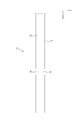
- the terminal-attached substrate 10 is mounted, for example, on a vehicle such as an automobile, and has a substrate 11 and a terminal 20 soldered to the substrate 11 as shown in FIG. 1.
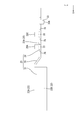
- the conductive path 13 made of copper foil or the like is formed on the insulating plate 12 via the adhesive layer 15 as shown in FIGS. There is.
- the substrate 11 for example, a flexible printed circuit (FPC) having flexibility capable of bending and deforming, or a rigid substrate having no flexibility can be used.
- the conductive paths 13 are formed only on the upper surface of the insulating plate 12.
- a conductive path may be formed on both upper and lower surfaces of the insulating plate 12 or a multilayer substrate having a plurality of conductive paths. It may be The rear side of the substrate 11 can be connected to the outside via, for example, a wire or the like.
- the left and right side edges of the substrate 11 are formed with insertion recesses 14 which are cut out in a rectangular shape. In the insertion recess 14, second protruding walls 30A and 30B of the terminal 20 described later are inserted.
- the terminal 20 is made of, for example, metal such as copper, copper alloy, aluminum, aluminum alloy, etc., and as shown in FIGS. 3 and 4, it is a female type and is connected to a male terminal (counter terminal) not shown.
- a terminal connection portion 21, a substrate connection portion 24 connected to the conductive path 13 of the substrate 11, and a connection portion 35 connecting the terminal connection portion 21 and the substrate connection portion 24 are provided.
- the terminal connection portion 21 extends inward from the inner wall of the rectangular cylindrical tube 22 having a rectangular rectangular shape in which the male terminal is inserted and the inner wall of the rectangular cylindrical portion 22 and is an elastic contact piece (not shown) contacting the male terminal. And.
- the rectangular tube portion 22 is formed by connecting a pair of upper and lower opposing walls 22A and 22C opposing each other and a pair of left and right side walls 22B and 22D connecting the pair of opposing walls 22A and 22C in an annular shape.
- the substrate connection portion 24 has a flat plate-like portion 25 and a plurality of projecting walls 28A to 28D, 30A, and 30B projecting upward and downward from the edge of the plate-like portion 25.
- the plate-like portion 25 has a strip-like portion 25A extending in a strip shape in the front-rear direction with a predetermined width dimension, and a plurality of extension pieces 26 flatly extended in the same plane from the side edge of the strip-like portion 25A.
- the plurality of extending pieces 26 are formed between the projecting walls 28A to 28D, 30A, and 30B adjacent to each other in the front and rear direction, and the tip in the extending direction of each extending piece 26 is the projecting walls 28A to 28D, 30A, and 30B. And the same position as the outer surface of.
- the tip of the extension piece 26 may be disposed inside the outer side surface of the projecting walls 28A to 28D, 30A, and 30B.
- the plurality of projecting walls 28A to 28D, 30A, and 30B project four (plural) first projecting walls 28A to 28D that project upward (opposite to the substrate 11) and the lower (substrate 11). It has two (plural) second protruding walls 30A, 30B.
- the first projecting walls 28A and 28B, the first projecting walls 28C and 28D, and the second projecting walls 30A and 30B are provided as a pair on the left and right, and the pair of left and right projecting walls are provided side by side in three sets (multiple sets) It is done.
- the projecting walls 28A to 28D, 30A, and 30B have a flat plate shape in a direction (intersecting direction) orthogonal to the strip 25A via the bending portion 31 bent from the side edges (edges on the side) of the strip 25A. Projected into The outer surface of the bent portion 31 is curved in a U-shape.
- the outer side surfaces 33 of the projecting walls 28A-28D, 30A, 30B are arranged in the same plane as the outer surfaces of the side walls 22B, 22D.
- the outer side surface 33 of the protruding walls 28A to 28D, 30A, and 30B may be disposed inside the outer surface of the side walls 22B and 22D.
- the tips of the first projecting walls 28A to 28D are disposed on the same plane as the upper surface of the opposing wall 22A of the rectangular tube portion 22.
- the tips of the first projecting walls 28A to 28D may be disposed below the same plane as the upper surface of the opposing wall 22A.
- the second projecting walls 30A, 30B project in the opposite direction to the first projecting walls 28A-28D, and the projecting dimensions of the second projecting walls 30A, 30B are smaller than the projecting dimensions of the first projecting walls 28A-28D. It is done.
- the corner of the tip (lower end) of the second projecting wall 30A, 30B is cut in a tapered shape and has a tapered shape.
- the connecting portion 35 extends in a state of being inclined with respect to the front and rear direction, and the front end is continuous with the facing wall 22A of the rectangular tube portion 22, and the rear end is continuous with the front end of the plate-like portion 25. Since the position of the plate-like portion 25 is disposed lower than the facing wall 22A by the connecting portion 35, the first projecting walls 28A to 28D are disposed above the plate-like portion 25 in the cavity 41 of the connector housing 40. Space is secured.
- the terminal 20 After forming the plating layer 37 which consists of tin etc. on the outer surface of a metal plate material, the terminal 20 is formed by giving stamping and bending process by a press (FIG. 3). In this state, the plated layer 37 is formed on the plate surface of the terminal 20 (see FIG. 7), but the cut end face of the terminal 20 by the press machine (the side end face of the plate-like portion 25 and the projecting walls 28A to 28D, The plating layer 37 is not formed on the tips 30A, 30B, etc., and the metal is exposed.
- solder paste is applied to the lower surface of the plate-like portion 25 or the upper surface of the substrate 11 and the terminals 20 are stacked on the substrate 11, the second projecting walls 30A and 30B are inserted into the insertion recesses 14 of the substrate 11. Then, the terminals 20 and the substrate 11 are subjected to reflow soldering, whereby the entire lower surface of the plate-like portion 25 is soldered to the conductive path 13 of the substrate 11, whereby the substrate 10 with terminals is formed. In this state, the solder S spreads from the plate-like portion 25 to the bending portion 31 on the base end side of the first projecting walls 28A to 28D, and a solder fillet is formed between the bending portion 31 and the conductive path 13 See Figure 7).
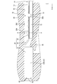
- the terminal-attached substrate 10 is accommodated in a synthetic resin connector housing 40 (only a part of the connector housing 40 is shown in FIG. 6).
- the connector housing 40 is to be fitted with the mating connector housing in which the male terminal is accommodated, and has a cavity 41 into which the terminal-attached substrate 10 is inserted.
- the cavity 41 has a rectangular side cross section and penetrates the connector housing 40 in the front-rear direction, and the front stop wall 42 annularly protrudes inward at the front end portion, and the rear end edge of the terminal connection portion 21
- a lance 44 is cantilevered from the inner wall of the cavity 41 to lock the terminal 20 and prevent the terminal 20 from being removed.
- the inside of the front blind wall 42 is a terminal insertion hole 43 into which the male terminal is inserted.
- the terminal connection portion 21 is held between the front stop wall 42 and the lance 44, and the substrate connection portion 24 is entirely accommodated in the cavity 41 and positioned. Be done. Although the rear side of the substrate 11 is led out from the cavity 41 in FIG. 6, the entire substrate 11 may be accommodated in the cavity 41.
- the terminal 20 has a terminal connection portion 21 connected to a mating terminal (male terminal) and a substrate connection portion 24 connected to the conductive path 13 of the substrate 11, and the substrate connection portion 24 is a terminal connection portion 21.
- a plate-like plate-like portion 25 which is disposed rearward and is soldered to the conductive path 13 of the substrate 11 and a plate which is bent from the side edge of the plate-like portion 25 and protrudes to the side opposite to the substrate 11 side ,
- a plating layer 37 is formed on the plate surfaces of the plate-like portion 25 and the first projecting walls 28A to 28D.
- the conductive path 13 of the substrate 11 is soldered to the plate-like portion 25 and the first projecting walls 28A to 28D are bent from the side edge of the plate-like portion 25 Protrudes on the opposite side.
- the solder S connecting the plate-like portion 25 and the conductive path 13 of the substrate 11 is formed on the base end side plating layer 37 of the first projecting walls 28A to 28D and is bent to the bent portion 31 having a bent plate surface. Since it can spread, it becomes possible to suppress the fall of intensity of soldering compared with the composition which makes the side edge of plate-like part 25 a cutting end face.
- the terminal connection portion 21 extends in a direction (crossing direction) orthogonal to the plate surface of the plate-like portion 25 and has a pair of side walls 22B and 22D disposed opposite to each other, and between the pair of side walls 22B and 22D
- the mating terminals are configured to be inserted therethrough, and the outer surfaces of the first projecting walls 28A to 28D are disposed on the same plane as the outer surfaces of the side walls 22B and 22D or inside the same plane. In this way, for example, when the terminals are inserted into the cavity 41 of the connector housing 40, the first projecting walls 28A to 28D are unlikely to be an obstacle to the insertion, so the insertion of the terminals into the cavity 41 of the connector housing 40 is facilitated. It can be carried out.
- the terminal connection portion 21 extends along the plate surface of the plate-like portion 25 and has a pair of opposing walls 22A and 22C disposed opposite to each other, and the mating terminal is inserted between the pair of opposing walls 22A and 22C.
- the projecting dimensions of the first projecting walls 28A to 28D are set so as not to project outward from the outer surfaces of the facing walls 22A and 22C. In this way, when the terminals are inserted into the cavity 41 of the connector housing 40, the first projecting walls 28A to 28D are unlikely to interfere with the insertion, so the terminals can be easily inserted into the cavity 41 of the connector housing 40. be able to.
- a plurality of first projecting walls 28A to 28D are provided in the front-rear direction. In this way, it is possible to suppress the overall occurrence of cracks occurring in the soldered portion.
- the second projecting walls 30A and 30B are disposed more rearward than the first projecting walls 28A to 28D. In this way, it is possible to suppress the occurrence of a defect in the solder on the rear side of the first projecting walls 28A to 28D in which stress is easily generated in the solder.
- the terminal 20 has second projecting walls 30A and 30B which are bent from the side edge of the plate-like portion 25 and project toward the substrate 11, and the substrate 11 is inserted with the second projecting walls 30A and 30B.
- the insertion recess 14 is provided. In this way, by inserting the second projecting walls 30A and 30B into the insertion recess 14, the terminal 20 can be positioned with respect to the substrate 11, and the terminal 20 is pulled backward with respect to the substrate 11. At this time, the second projecting walls 30A, 30B can be engaged with the insertion recess 14 to reduce the stress generated in the soldered portion.
- the terminal-attached substrate 50 of the second embodiment is obtained by changing the thickness of the substrate 11 with respect to the terminal-attached substrate 10 of the first embodiment. Since the other configuration is the same as that of the first embodiment, the same reference numerals are given to the same configuration as the first embodiment and the description will be omitted.
- the terminal-attached substrate 50 includes a terminal 20 and a substrate 51 to which the terminal 20 is soldered.
- the substrate 51 is, for example, a flexible printed circuit board, and is in the form of a long plate in the front-rear direction, and a conductive path 13 made of copper foil or the like is formed on the insulating plate 12 with the adhesive layer 15 interposed therebetween.
- the side edge portion of the substrate 11 is formed with an insertion recess 52 cut in a rectangular shape. In the insertion recess 52, the second projecting walls 30A and 30B of the terminal 20 are inserted, and the tip end of the second projecting walls 30A and 30B penetrates the insertion recess 52.
- the rear side of the substrate 51 is connected to the outside through, for example, a wire or the like.
- the thickness of the substrate 51 is formed to be equal to or slightly larger than the thickness of the plate-like portion 25.
- a reinforcing plate may be stacked on the substrate 51, or may be inserted into the cavity 41 in a state where the reinforcing plate is stacked on the substrate 51.
- first projecting walls 28A to 28D and the second projecting walls 30A and 30B project in the direction orthogonal to the plate surface of the plate-like portion 25, but the present invention is not limited thereto. For example, it may protrude in the direction inclined with respect to the plate surface of the plate-like part 25.
- the projecting dimensions of the first projecting walls 28A to 28D and the second projecting walls 30A and 30B are not limited to the dimensions of the above embodiment, and can be different projecting dimensions.
- the protrusion dimensions of the first projecting walls 28A to 28D may be reduced to at least the solder fillet to be formed in the bent portion 31.
- the number of the first projecting walls 28A to 28D and the second projecting walls 30A and 30B is not limited to the number in the above embodiment.
- the number of the first projecting walls 28A to 28D and the second projecting walls 30A and 30B may be one.
- only the first projecting walls 28A to 28D may be provided without providing the second projecting walls 30A and 30B.
- the first projecting wall may be provided along the entire length in the front-rear direction of the side edge portion of the plate-like portion 25 and soldered to the substrates 11 and 51.
- terminal-provided substrate 11 51: substrate 12: insulating plate 13: conductive path 14, 52: insertion recess 20: terminal 21: terminal connection portion 22: square tube portion 22A, 22C: facing wall 22B, 22D: side wall 24: Substrate connecting portion 25: Plate-like portions 28A to 28D: first projecting wall 30A, 30B: second projecting wall 31: bent portion 40: connector housing 41: cavity
Landscapes
- Coupling Device And Connection With Printed Circuit (AREA)
Abstract
相手側端子と接続される端子接続部21と基板11の導電路13に接続される基板接続部24とを有する端子20であって、基板接続部24は、端子接続部21の後方に配され、基板11の導電路13に半田付けされる板状の板状部25と、板状部25の側方側の縁部から曲がって基板11側とは反対側に突出する板状の第1突壁28A~28Dと、を有し、板状部25及び第1突壁28A~28Dの板面にはメッキ層37が形成されている。
Description
本明細書では、端子及び端子付き基板に関する技術を開示する。
従来、基板の導電路に端子が半田付けされる技術が知られている。特許文献1では、プラグ絶縁体に複数のプラグ端子が固定されたコネクタが記載されており、プラグ絶縁体の背面から延出された複数のプラグ端子は、オフセット曲げされた先端部が回路基板の表面の接続電極に半田付けされている。
ところで、基板に半田付けされる端子は、一般に、金属板材にメッキを施した後、プレス機により打ち抜き加工を施して形成されている。したがって、図9に示すように、端子1の上下の板面には、メッキ層2A,2Bが形成されているが、プレス機による切断端面3A,3Bとなる端子1の左右には、メッキ層が形成されていない。基板4上に接着剤8を介して重ねられた銅箔6に対して端子1を半田付けする場合、メッキ層2Bが形成された端子1の下面と銅箔6とは半田付けすることができるが、メッキ層が形成されていない端子1の左右の切断端面3A,3Bには半田7が広がらないため、半田付けの強度の低下が懸念される。
本明細書に記載された技術は、上記のような事情に基づいて完成されたものであって、基板に半田付けされる端子について半田付けの強度の低下を抑制することを目的とする。
本明細書に記載された端子は、相手側端子と接続される端子接続部と基板の導電路に接続される基板接続部とを有する端子であって、前記基板接続部は、前記端子接続部の後方に配され、前記基板の導電路に半田付けされる板状の板状部と、前記板状部の側方側の縁部から曲がって前記基板側とは反対側に突出する板状の第1突壁と、を有し、前記板状部及び前記第1突壁の板面には、メッキ層が形成されている。
上記構成によれば、基板の導電路は板状部に半田付けされるとともに、第1突壁が板状部の側方側の縁部から曲がって基板とは反対側に突出することにより、板状部と基板の導電路とを接続する半田は第1突壁の基端側のメッキ層が形成されて曲がった部分に広がることができるため、板状部の側縁部が切断端面とされる構成と比較して、半田付けの強度の低下を抑制することが可能になる。
本明細書に記載された技術の実施態様としては以下の態様が好ましい。
前記端子接続部は、前記板状部の板面と交差する方向に延び、互いに対向配置された一対の側壁を有し、前記一対の側壁間に前記相手側端子が挿通されるように構成されており、前記第1突壁の外面は、前記側壁の外面と同一平面又は前記同一平面よりも内側に配されている。
このようにすれば、例えばコネクタハウジングのキャビティに端子を挿入する際に第1突壁が挿入の障害になりにくいため、コネクタハウジングのキャビティへの端子の挿入を容易に行うことができる。
前記端子接続部は、前記板状部の板面と交差する方向に延び、互いに対向配置された一対の側壁を有し、前記一対の側壁間に前記相手側端子が挿通されるように構成されており、前記第1突壁の外面は、前記側壁の外面と同一平面又は前記同一平面よりも内側に配されている。
このようにすれば、例えばコネクタハウジングのキャビティに端子を挿入する際に第1突壁が挿入の障害になりにくいため、コネクタハウジングのキャビティへの端子の挿入を容易に行うことができる。
前記端子接続部は、前記板状部の板面に沿って延び、互いに対向配置された一対の対向壁を有し、前記一対の対向壁間に前記相手側端子が挿通されるように構成されており、前記第1突壁の突出寸法は、前記対向壁の外面よりも外方に突出しない寸法に設定されている。
このようにすれば、コネクタハウジングのキャビティに端子を挿入する際に第1突壁が挿入の障害になりにくいため、コネクタハウジングのキャビティへの端子の挿入を容易に行うことができる。
このようにすれば、コネクタハウジングのキャビティに端子を挿入する際に第1突壁が挿入の障害になりにくいため、コネクタハウジングのキャビティへの端子の挿入を容易に行うことができる。
前記第1突壁は、前後方向に複数設けられている。
このようにすれば、半田付けされた箇所に生じるクラックが全体に及ぶことを抑制することができる。
このようにすれば、半田付けされた箇所に生じるクラックが全体に及ぶことを抑制することができる。
前記第1突壁は、前記板状部の左右の縁部に一対設けられている。
前記板状部の側方側の縁部から曲がって前記基板側に突出する第2突壁を有する。
このようにすれば、第2突壁を基板に係止させることにより、基板に対して端子に力が加えられた際に、半田付けされた部分に生じる応力を低減することができる。
このようにすれば、第2突壁を基板に係止させることにより、基板に対して端子に力が加えられた際に、半田付けされた部分に生じる応力を低減することができる。
前記第2突壁は、前記第1突壁よりも後方側に配されている。
このようにすれば、半田にストレスが生じやすい第1突壁の後方側について半田に不具合が生じることを抑制することができる。
このようにすれば、半田にストレスが生じやすい第1突壁の後方側について半田に不具合が生じることを抑制することができる。
前記端子と、前記基板とを備える、端子付き基板とする。
前記端子は、前記板状部の側方側の縁部から曲がって前記基板側に突出する第2突壁を有し、前記基板は、前記第2突壁が挿通される挿通凹部を備える、端子付き基板とする。
このようにすれば、第2突壁が挿通凹部に挿通されることにより、基板に対する端子の位置決めをすることができるとともに、基板に対して端子が後方に引っ張られた際に、第2突壁が挿通凹部に係止し、半田付けされた部分に生じる応力を低減することが可能になる。
このようにすれば、第2突壁が挿通凹部に挿通されることにより、基板に対する端子の位置決めをすることができるとともに、基板に対して端子が後方に引っ張られた際に、第2突壁が挿通凹部に係止し、半田付けされた部分に生じる応力を低減することが可能になる。
本明細書に記載された技術によれば、基板に半田付けされる端子について半田付けの強度の低下を抑制することが可能になる。
<実施形態1>
実施形態1について、図1~図7を参照しつつ説明する。以下では、図3のX方向を前方、Y方向を左方、Z方向を上方として説明する。
(端子付き基板10)
端子付き基板10は、例えば自動車等の車両に搭載され、図1に示すように、基板11と、基板11に半田付けされる端子20とを有する。
実施形態1について、図1~図7を参照しつつ説明する。以下では、図3のX方向を前方、Y方向を左方、Z方向を上方として説明する。
(端子付き基板10)
端子付き基板10は、例えば自動車等の車両に搭載され、図1に示すように、基板11と、基板11に半田付けされる端子20とを有する。
(基板11)
基板11は、図1,図2に示すように、絶縁板12の上に接着剤層15を介して銅箔等からなる導電路13が形成されており、前後方向に長い板状とされている。この基板11としては、例えば、撓み変形可能な柔軟性を有するフレキシブルプリント基板(FPC)や、柔軟性を有さないリジッド基板を用いることができる。本実施形態では、絶縁板12の上面のみに導電路13が形成されているが、これに限られず、絶縁板12の上下両面に導電路を形成したり、複数層の導電路を有する多層基板としてもよい。基板11の後方側は、例えば電線等を介して外部と接続することができる。基板11の左右の側縁部は、長方形状に切り欠かれた挿通凹部14が形成されている。挿通凹部14は、後述する端子20の第2突壁30A,30Bが挿通される。
基板11は、図1,図2に示すように、絶縁板12の上に接着剤層15を介して銅箔等からなる導電路13が形成されており、前後方向に長い板状とされている。この基板11としては、例えば、撓み変形可能な柔軟性を有するフレキシブルプリント基板(FPC)や、柔軟性を有さないリジッド基板を用いることができる。本実施形態では、絶縁板12の上面のみに導電路13が形成されているが、これに限られず、絶縁板12の上下両面に導電路を形成したり、複数層の導電路を有する多層基板としてもよい。基板11の後方側は、例えば電線等を介して外部と接続することができる。基板11の左右の側縁部は、長方形状に切り欠かれた挿通凹部14が形成されている。挿通凹部14は、後述する端子20の第2突壁30A,30Bが挿通される。
(端子20)
端子20は、例えば、銅、銅合金、アルミニウム、アルミニウム合金等の金属からなり、図3,図4に示すように、雌型であって、図示しない雄端子(相手側端子)と接続される端子接続部21と、基板11の導電路13に接続される基板接続部24と、端子接続部21と基板接続部24とを連結する連結部35とを有する。
端子20は、例えば、銅、銅合金、アルミニウム、アルミニウム合金等の金属からなり、図3,図4に示すように、雌型であって、図示しない雄端子(相手側端子)と接続される端子接続部21と、基板11の導電路13に接続される基板接続部24と、端子接続部21と基板接続部24とを連結する連結部35とを有する。
端子接続部21は、雄端子が内部に挿通される長方形の角筒状の角筒部22と、角筒部22の内壁から内方に延び、雄端子に接触する弾性接触片(図示しない)とを有する。角筒部22は、互いに対向する上下一対の対向壁22A,22Cと、一対の対向壁22A,22C間を連結する左右一対の側壁22B,22Dとを環状に連ねて形成されている。
基板接続部24は、平板状の板状部25と、板状部25の縁部から上下に突出する複数の突壁28A~28D,30A,30Bとを有する。板状部25は、所定の幅寸法で前後方向に帯状に延びる帯状部25Aと、帯状部25Aの側縁から側方の同一平面に平板状に延出された複数の延出片26とを有する。
複数の延出片26は、前後に隣り合う突壁28A~28D,30A,30B間に形成されており、各延出片26の延出方向の先端は、突壁28A~28D,30A,30Bの外側面とほぼ同じ位置とされている。なお、延出片26の先端を突壁28A~28D,30A,30Bの外側面より内側に配する構成としてもよい。複数の突壁28A~28D,30A,30Bは、上方(基板11側とは反対側)に突出する4つ(複数)の第1突壁28A~28Dと、下方(基板11側)に突出する2つ(複数)の第2突壁30A,30Bとを有する。第1突壁28A,28B、第1突壁28C,28D及び第2突壁30A,30Bは、左右一対設けられており、左右一対の突壁は、前後に並んで3組(複数組)設けられている。突壁28A~28D,30A,30Bは、帯状部25Aの両側縁部(側方側の縁部)から曲がった曲げ部31を介して帯状部25Aと直交する方向(交差する方向)に平板状に突出している。曲げ部31の外面は、U字状に湾曲した形状とされている。
突壁28A~28D,30A,30Bの外側面33は、側壁22B,22Dの外面と同一平面に配されている。なお、他の実施形態として突壁28A~28D,30A,30Bの外側面33が側壁22B,22Dの外面よりも内側に配される構成としてもよい。第1突壁28A~28Dは、図5に示すように、先端が角筒部22の対向壁22Aの上面と同一平面に配されている。なお、他の実施形態として第1突壁28A~28Dの先端が対向壁22Aの上面と同一平面よりも下側に配される構成としてもよい。第2突壁30A,30Bは、第1突壁28A~28Dとは反対方向に突出しており、第2突壁30A,30Bの突出寸法は、第1突壁28A~28Dの突出寸法よりも小さくされている。第2突壁30A,30Bの先端部(下端部)の角部は、テーパ状に切り欠かれて先細形状となっている。
連結部35は、前後方向に対して傾斜した状態で延びており、前端が角筒部22の対向壁22Aに連なり、後端が板状部25の前端に連なっている。連結部35により、板状部25の位置が対向壁22Aよりも下側に配されるため、コネクタハウジング40のキャビティ41内において板状部25の上方に第1突壁28A~28Dが配されるスペースが確保される。
端子付き基板10の製造方法について説明する。
金属板材の外面に例えばスズ等からなるメッキ層37を形成した後、プレス機により、打ち抜き加工及び曲げ加工を施すことにより、端子20が形成される(図3)。この状態では、端子20の板面には、メッキ層37が形成されているが(図7参照)、プレス機による端子20の切断端面(板状部25の側端面や突壁28A~28D,30A,30Bの先端等)には、メッキ層37がされておらず、金属が露出した状態とされる。
金属板材の外面に例えばスズ等からなるメッキ層37を形成した後、プレス機により、打ち抜き加工及び曲げ加工を施すことにより、端子20が形成される(図3)。この状態では、端子20の板面には、メッキ層37が形成されているが(図7参照)、プレス機による端子20の切断端面(板状部25の側端面や突壁28A~28D,30A,30Bの先端等)には、メッキ層37がされておらず、金属が露出した状態とされる。
そして、板状部25の下面又は基板11の上面に半田ペーストを塗布し、基板11の上に端子20を重ねると、基板11の挿通凹部14に第2突壁30A,30Bが挿通される。そして、端子20と基板11とをリフロー半田付けをすることにより、板状部25の下面の全体が基板11の導電路13に半田付けされた状態となり、端子付き基板10が形成される。この状態では、板状部25から第1突壁28A~28Dの基端側の曲げ部31にまで半田Sが広がって曲げ部31と導電路13との間に半田フィレットが形成されている(図7参照)。
端子付き基板10は、図6に示すように、合成樹脂製のコネクタハウジング40(図6では、コネクタハウジング40の一部のみ図示)に収容される。コネクタハウジング40は、雄端子が収容された相手側コネクタハウジングと嵌合するものであり、端子付き基板10が挿通されるキャビティ41を有する。キャビティ41は、長方形状の側断面を有し、コネクタハウジング40を前後方向に貫通しており、前端部に前止まり壁42が内方に環状に突出するとともに、端子接続部21の後端縁に係止して端子20を抜け止めするランス44がキャビティ41の内壁から片持ち状に延びている。前止まり壁42の内側は、雄端子が挿通される端子挿通孔43とされている。
端子付き基板10がキャビティ41の正規位置に収容されると、端子接続部21が前止まり壁42とランス44との間に保持され、基板接続部24は、全体がキャビティ41に収容されて位置決めされる。なお、図6では基板11の後方側はキャビティ41から外部に導出されているが、基板11の全体をキャビティ41に収容してもよい。
本実施形態によれば、以下の作用、効果を奏する。
相手側端子(雄端子)と接続される端子接続部21と基板11の導電路13に接続される基板接続部24とを有する端子20であって、基板接続部24は、端子接続部21の後方に配され、基板11の導電路13に半田付けされる板状の板状部25と、板状部25の側方側の縁部から曲がって基板11側とは反対側に突出する板状の第1突壁28A~28Dと、を有し、板状部25及び第1突壁28A~28Dの板面にはメッキ層37が形成されている。
本実施形態によれば、基板11の導電路13は板状部25に半田付けされるとともに、第1突壁28A~28Dが板状部25の側方側の縁部から曲がって基板11とは反対側に突出する。これにより、板状部25と基板11の導電路13とを接続する半田Sは第1突壁28A~28Dの基端側のメッキ層37が形成されて曲がった板面を有する曲げ部31に広がることができるため、板状部25の側縁部が切断端面とされる構成と比較して、半田付けの強度の低下を抑制することが可能になる。
相手側端子(雄端子)と接続される端子接続部21と基板11の導電路13に接続される基板接続部24とを有する端子20であって、基板接続部24は、端子接続部21の後方に配され、基板11の導電路13に半田付けされる板状の板状部25と、板状部25の側方側の縁部から曲がって基板11側とは反対側に突出する板状の第1突壁28A~28Dと、を有し、板状部25及び第1突壁28A~28Dの板面にはメッキ層37が形成されている。
本実施形態によれば、基板11の導電路13は板状部25に半田付けされるとともに、第1突壁28A~28Dが板状部25の側方側の縁部から曲がって基板11とは反対側に突出する。これにより、板状部25と基板11の導電路13とを接続する半田Sは第1突壁28A~28Dの基端側のメッキ層37が形成されて曲がった板面を有する曲げ部31に広がることができるため、板状部25の側縁部が切断端面とされる構成と比較して、半田付けの強度の低下を抑制することが可能になる。
また、端子接続部21は、板状部25の板面と直交する方向(交差する方向)に延び、互いに対向配置された一対の側壁22B,22Dを有し、一対の側壁22B,22D間に相手側端子が挿通されるように構成されており、第1突壁28A~28Dの外面は、側壁22B,22Dの外面と同一平面又は同一平面よりも内側に配されている。
このようにすれば、例えばコネクタハウジング40のキャビティ41に端子を挿入する際に第1突壁28A~28Dが挿入の障害になりにくいため、コネクタハウジング40のキャビティ41への端子の挿入を容易に行うことができる。
このようにすれば、例えばコネクタハウジング40のキャビティ41に端子を挿入する際に第1突壁28A~28Dが挿入の障害になりにくいため、コネクタハウジング40のキャビティ41への端子の挿入を容易に行うことができる。
また、端子接続部21は、板状部25の板面に沿って延び、互いに対向配置された一対の対向壁22A,22Cを有し、一対の対向壁22A,22C間に相手側端子が挿通されるように構成されており、第1突壁28A~28Dの突出寸法は、対向壁22A,22Cの外面よりも外方に突出しない寸法に設定されている。
このようにすれば、コネクタハウジング40のキャビティ41に端子を挿入する際に第1突壁28A~28Dが挿入の障害になりにくいため、コネクタハウジング40のキャビティ41への端子の挿入を容易に行うことができる。
このようにすれば、コネクタハウジング40のキャビティ41に端子を挿入する際に第1突壁28A~28Dが挿入の障害になりにくいため、コネクタハウジング40のキャビティ41への端子の挿入を容易に行うことができる。
第1突壁28A~28Dは、前後方向に複数設けられている。
このようにすれば、半田付けされた箇所に生じるクラックが全体に及ぶことを抑制することができる。
このようにすれば、半田付けされた箇所に生じるクラックが全体に及ぶことを抑制することができる。
第2突壁30A,30Bは、第1突壁28A~28Dよりも後方側に配されている。
このようにすれば、半田にストレスが生じやすい第1突壁28A~28Dの後方側について半田に不具合が生じることを抑制することができる。
このようにすれば、半田にストレスが生じやすい第1突壁28A~28Dの後方側について半田に不具合が生じることを抑制することができる。
また、端子20は、板状部25の側方側の縁部から曲がって基板11側に突出する第2突壁30A,30Bを有し、基板11は、第2突壁30A,30Bが挿通される挿通凹部14を備える。
このようにすれば、第2突壁30A,30Bが挿通凹部14に挿通されることにより、基板11に対する端子20の位置決めをすることができるとともに、基板11に対して端子20が後方に引っ張られた際に、第2突壁30A,30Bが挿通凹部14に係止し、半田付けされた部分に生じる応力を低減することが可能になる。
このようにすれば、第2突壁30A,30Bが挿通凹部14に挿通されることにより、基板11に対する端子20の位置決めをすることができるとともに、基板11に対して端子20が後方に引っ張られた際に、第2突壁30A,30Bが挿通凹部14に係止し、半田付けされた部分に生じる応力を低減することが可能になる。
<実施形態2>
次に、実施形態2について図8を参照しつつ説明する。実施形態2の端子付き基板50は、実施形態1の端子付き基板10に対して基板11の厚みを変えたものである。他の構成は実施形態1と同一であるため、実施形態1と同一の構成については同一の符号を付して説明を省略する。
次に、実施形態2について図8を参照しつつ説明する。実施形態2の端子付き基板50は、実施形態1の端子付き基板10に対して基板11の厚みを変えたものである。他の構成は実施形態1と同一であるため、実施形態1と同一の構成については同一の符号を付して説明を省略する。
端子付き基板50は、端子20と、端子20が半田付けされる基板51とを備える。基板51は、例えば、フレキシブルプリント基板であって、前後方向に長い板状とされ、絶縁板12の上に接着剤層15を介して銅箔等からなる導電路13が形成されている。基板11の側縁部は、長方形状に切り欠かれた挿通凹部52が形成されている。挿通凹部52は、端子20の第2突壁30A,30Bが挿通されて、第2突壁30A,30Bの先端が挿通凹部52を貫通する。基板51の後方側は、例えば電線等を介して外部と接続される。基板51の厚みは、板状部25の厚みと同等か板状部25よりもわずかに厚く形成されている。なお、図示はしないが、基板51に補強板を重ねてもよく、基板51に補強板を重ねた状態でキャビティ41に挿通されるようにしてもよい。
<他の実施形態>
本明細書に記載された技術は上記記述及び図面によって説明した実施形態に限定されるものではなく、例えば次のような実施形態も本明細書に記載された技術の技術的範囲に含まれる。
(1)第1突壁28A~28D及び第2突壁30A,30Bは、板状部25の板面に対して直交する方向に突出していたが、これに限られない。例えば、板状部25の板面に対して傾斜した方向に突出していてもよい。
本明細書に記載された技術は上記記述及び図面によって説明した実施形態に限定されるものではなく、例えば次のような実施形態も本明細書に記載された技術の技術的範囲に含まれる。
(1)第1突壁28A~28D及び第2突壁30A,30Bは、板状部25の板面に対して直交する方向に突出していたが、これに限られない。例えば、板状部25の板面に対して傾斜した方向に突出していてもよい。
(2)第1突壁28A~28D及び第2突壁30A,30Bの突出寸法は、上記実施形態の寸法に限られず、異なる突出寸法とすることができる。例えば、第1突壁28A~28Dの突出寸法を小さくして、少なくとも半田フィレットが曲げ部31に形成される突出寸法としてもよい。
(3)第1突壁28A~28D及び第2突壁30A,30Bの数は、上記実施形態の数に限られない。例えば、第1突壁28A~28Dや第2突壁30A,30Bの数を1つとしてもよい。また、第2突壁30A,30Bを設けず、第1突壁28A~28Dのみを設けてもよい。また、板状部25の側縁部について前後方向の全長に亘って第1突壁を設けて基板11,51に半田付けするようにしてもよい。
10,50: 端子付き基板
11,51: 基板
12: 絶縁板
13: 導電路
14,52: 挿通凹部
20: 端子
21: 端子接続部
22: 角筒部
22A,22C: 対向壁
22B,22D: 側壁
24: 基板接続部
25: 板状部
28A~28D: 第1突壁
30A,30B: 第2突壁
31: 曲げ部
40: コネクタハウジング
41: キャビティ
11,51: 基板
12: 絶縁板
13: 導電路
14,52: 挿通凹部
20: 端子
21: 端子接続部
22: 角筒部
22A,22C: 対向壁
22B,22D: 側壁
24: 基板接続部
25: 板状部
28A~28D: 第1突壁
30A,30B: 第2突壁
31: 曲げ部
40: コネクタハウジング
41: キャビティ
Claims (9)
- 相手側端子と接続される端子接続部と基板の導電路に接続される基板接続部とを有する端子であって、
前記基板接続部は、前記端子接続部の後方に配され、前記基板の導電路に半田付けされる板状の板状部と、前記板状部の側方側の縁部から曲がって前記基板側とは反対側に突出する板状の第1突壁と、を有し、
前記板状部及び前記第1突壁の板面には、メッキ層が形成されている、端子。 - 前記端子接続部は、前記板状部の板面と交差する方向に延び、互いに対向配置された一対の側壁を有し、前記一対の側壁間に前記相手側端子が挿通されるように構成されており、
前記第1突壁の外面は、前記側壁の外面と同一平面又は前記同一平面よりも内側に配されている請求項1に記載の端子。 - 前記端子接続部は、前記板状部の板面に沿って延び、互いに対向配置された一対の対向壁を有し、前記一対の対向壁間に前記相手側端子が挿通されるように構成されており、
前記第1突壁の突出寸法は、前記対向壁の外面よりも外方に突出しない寸法に設定されている請求項1又は請求項2に記載の端子。 - 前記第1突壁は、前後方向に複数設けられている請求項1から請求項3のいずれか一項に記載の端子。
- 前記第1突壁は、前記板状部の左右の縁部に一対設けられている請求項1から請求項4のいずれか一項に記載の端子。
- 前記板状部の側方側の縁部から曲がって前記基板側に突出する第2突壁を有する請求項1から請求項5のいずれか一項に記載の端子。
- 前記第2突壁は、前記第1突壁よりも後方側に配されている請求項6に記載の端子。
- 請求項1から請求項7のいずれか一項に記載の端子と、前記基板とを備える、端子付き基板。
- 前記端子は、前記板状部の側方側の縁部から曲がって前記基板側に突出する第2突壁を有し、前記基板は、前記第2突壁が挿通される挿通凹部を備える、請求項8に記載の端子付き基板。
Priority Applications (2)
| Application Number | Priority Date | Filing Date | Title |
|---|---|---|---|
| CN201880044486.5A CN110832705A (zh) | 2017-07-13 | 2018-06-28 | 端子及带有端子的基板 |
| US16/630,067 US10965046B2 (en) | 2017-07-13 | 2018-06-28 | Board with terminal |
Applications Claiming Priority (2)
| Application Number | Priority Date | Filing Date | Title |
|---|---|---|---|
| JP2017-137177 | 2017-07-13 | ||
| JP2017137177A JP2019021443A (ja) | 2017-07-13 | 2017-07-13 | 端子及び端子付き基板 |
Publications (1)
| Publication Number | Publication Date |
|---|---|
| WO2019013000A1 true WO2019013000A1 (ja) | 2019-01-17 |
Family
ID=65001288
Family Applications (1)
| Application Number | Title | Priority Date | Filing Date |
|---|---|---|---|
| PCT/JP2018/024519 Ceased WO2019013000A1 (ja) | 2017-07-13 | 2018-06-28 | 端子及び端子付き基板 |
Country Status (4)
| Country | Link |
|---|---|
| US (1) | US10965046B2 (ja) |
| JP (1) | JP2019021443A (ja) |
| CN (1) | CN110832705A (ja) |
| WO (1) | WO2019013000A1 (ja) |
Families Citing this family (1)
| Publication number | Priority date | Publication date | Assignee | Title |
|---|---|---|---|---|
| CN114097309A (zh) * | 2019-07-10 | 2022-02-25 | 住友电工印刷电路株式会社 | 柔性印刷配线板、电池配线模块及柔性印刷配线板的制造方法 |
Citations (6)
| Publication number | Priority date | Publication date | Assignee | Title |
|---|---|---|---|---|
| JP2003187916A (ja) * | 2001-12-20 | 2003-07-04 | Tyco Electronics Amp Kk | シールド型コネクタ |
| JP2007087930A (ja) * | 2005-08-25 | 2007-04-05 | Kyoshin Kogyo Co Ltd | ねじ端子 |
| JP2010251135A (ja) * | 2009-04-16 | 2010-11-04 | Hosiden Corp | メス側端子及び基板間接続構造 |
| JP2013534032A (ja) * | 2010-07-06 | 2013-08-29 | 日本圧着端子製造株式会社 | 確実にはんだ付けが可能な電気部品 |
| JP2015118872A (ja) * | 2013-12-19 | 2015-06-25 | 株式会社デンソー | 電子基板 |
| JP2016096021A (ja) * | 2014-11-14 | 2016-05-26 | 住友電装株式会社 | 基板端子付プリント基板およびそれを用いた電気接続箱 |
Family Cites Families (15)
| Publication number | Priority date | Publication date | Assignee | Title |
|---|---|---|---|---|
| JP2913359B2 (ja) * | 1993-12-14 | 1999-06-28 | 本多通信工業株式会社 | Pcカード用コネクタ |
| JP2928987B2 (ja) * | 1995-03-31 | 1999-08-03 | 日本航空電子工業株式会社 | コンタクト及びその製造方法 |
| JP3085572B2 (ja) * | 1995-10-13 | 2000-09-11 | エスエムケイ株式会社 | 接続用端子 |
| JPH11121114A (ja) | 1997-08-12 | 1999-04-30 | Fujitsu Takamisawa Component Ltd | 基板実装用コネクタ |
| JP2001319715A (ja) * | 2000-05-09 | 2001-11-16 | Moldec Kk | 表面実装用電子部品及び回路基板の電極 |
| JP4135890B2 (ja) * | 2002-10-02 | 2008-08-20 | ローム株式会社 | フラットフレキシブルケーブルの耐熱性回路基板に対する半田接続方法 |
| US7309252B2 (en) * | 2005-02-22 | 2007-12-18 | Tyco Electronics Corporation | Low profile surface mount connector |
| JP4854471B2 (ja) * | 2006-10-27 | 2012-01-18 | 京セラ株式会社 | ラグ端子及び回路基板並びに電子モジュール |
| JP5541991B2 (ja) * | 2010-07-20 | 2014-07-09 | タイコエレクトロニクスジャパン合同会社 | 表面実装型コンタクト及びそれを用いたコネクタ |
| JP5638934B2 (ja) * | 2010-12-24 | 2014-12-10 | 矢崎総業株式会社 | 端子 |
| JP5683284B2 (ja) * | 2011-01-14 | 2015-03-11 | 矢崎総業株式会社 | 基板接続用端子 |
| JP5129372B1 (ja) * | 2011-08-01 | 2013-01-30 | イリソ電子工業株式会社 | 電気接続用端子及びその実装方法 |
| EP2833480B1 (en) * | 2012-03-28 | 2018-09-12 | Japan Aviation Electronics Industry, Ltd. | Electric wire-substrate connector |
| JP6033164B2 (ja) * | 2013-05-23 | 2016-11-30 | オムロンオートモーティブエレクトロニクス株式会社 | 端子、電子制御装置 |
| JP6806482B2 (ja) * | 2016-07-21 | 2021-01-06 | 日本航空電子工業株式会社 | コネクタ |
-
2017
- 2017-07-13 JP JP2017137177A patent/JP2019021443A/ja active Pending
-
2018
- 2018-06-28 WO PCT/JP2018/024519 patent/WO2019013000A1/ja not_active Ceased
- 2018-06-28 US US16/630,067 patent/US10965046B2/en not_active Expired - Fee Related
- 2018-06-28 CN CN201880044486.5A patent/CN110832705A/zh active Pending
Patent Citations (6)
| Publication number | Priority date | Publication date | Assignee | Title |
|---|---|---|---|---|
| JP2003187916A (ja) * | 2001-12-20 | 2003-07-04 | Tyco Electronics Amp Kk | シールド型コネクタ |
| JP2007087930A (ja) * | 2005-08-25 | 2007-04-05 | Kyoshin Kogyo Co Ltd | ねじ端子 |
| JP2010251135A (ja) * | 2009-04-16 | 2010-11-04 | Hosiden Corp | メス側端子及び基板間接続構造 |
| JP2013534032A (ja) * | 2010-07-06 | 2013-08-29 | 日本圧着端子製造株式会社 | 確実にはんだ付けが可能な電気部品 |
| JP2015118872A (ja) * | 2013-12-19 | 2015-06-25 | 株式会社デンソー | 電子基板 |
| JP2016096021A (ja) * | 2014-11-14 | 2016-05-26 | 住友電装株式会社 | 基板端子付プリント基板およびそれを用いた電気接続箱 |
Also Published As
| Publication number | Publication date |
|---|---|
| US20200366009A1 (en) | 2020-11-19 |
| JP2019021443A (ja) | 2019-02-07 |
| US10965046B2 (en) | 2021-03-30 |
| CN110832705A (zh) | 2020-02-21 |
Similar Documents
| Publication | Publication Date | Title |
|---|---|---|
| JP5221313B2 (ja) | 端子金具 | |
| JP6006356B2 (ja) | コンタクト及び該コンタクトを使用するコネクタ | |
| JP5737361B2 (ja) | コネクタ端子 | |
| US7341462B2 (en) | Connector terminal fabrication process and connector terminal | |
| CN104103925B (zh) | 电触头和包括其的电连接器组件 | |
| JP6225313B2 (ja) | 圧着接続端子及びその製造方法 | |
| JP5614484B1 (ja) | 電気コネクタの接合部材およびその製造方法 | |
| US11088476B2 (en) | Board connector with chained terminals | |
| US20180248291A1 (en) | Board connector | |
| US20140287604A1 (en) | Terminal, terminal module and method of manufacuring the terminal module | |
| JP2016149336A (ja) | ピン端子、端子群及びコネクタ | |
| JP7210186B2 (ja) | 回路基板組立体 | |
| WO2019013000A1 (ja) | 端子及び端子付き基板 | |
| JP2013149578A (ja) | 接続端子 | |
| JP5799697B2 (ja) | コンタクト部材およびその製造方法 | |
| JP2015177039A (ja) | プリント基板およびそれを用いた端子付プリント基板 | |
| WO2021192889A1 (ja) | 端子、基板用コネクタ、及び端子の製造方法 | |
| JP6988745B2 (ja) | コネクタ | |
| US20170346203A1 (en) | Board terminal | |
| KR20050050581A (ko) | 억지 끼워맞춤용 컨택트 및 이것을 이용한 억지 끼워맞춤커넥터 | |
| JP6506876B1 (ja) | 圧着接続端子 | |
| US20160190714A1 (en) | Terminal and connection structure using terminal | |
| JP4187217B2 (ja) | コネクタ | |
| TWM495013U (zh) | 卡緣連接器及卡緣連接器組合 | |
| JP2012190708A (ja) | 接続端子 |
Legal Events
| Date | Code | Title | Description |
|---|---|---|---|
| 121 | Ep: the epo has been informed by wipo that ep was designated in this application |
Ref document number: 18831540 Country of ref document: EP Kind code of ref document: A1 |
|
| NENP | Non-entry into the national phase |
Ref country code: DE |
|
| 122 | Ep: pct application non-entry in european phase |
Ref document number: 18831540 Country of ref document: EP Kind code of ref document: A1 |