WO2018230233A1 - マスクブランク、位相シフトマスク及び半導体デバイスの製造方法 - Google Patents
マスクブランク、位相シフトマスク及び半導体デバイスの製造方法 Download PDFInfo
- Publication number
- WO2018230233A1 WO2018230233A1 PCT/JP2018/018872 JP2018018872W WO2018230233A1 WO 2018230233 A1 WO2018230233 A1 WO 2018230233A1 JP 2018018872 W JP2018018872 W JP 2018018872W WO 2018230233 A1 WO2018230233 A1 WO 2018230233A1
- Authority
- WO
- WIPO (PCT)
- Prior art keywords
- phase shift
- film
- light
- lower layer
- upper layer
- Prior art date
- Legal status (The legal status is an assumption and is not a legal conclusion. Google has not performed a legal analysis and makes no representation as to the accuracy of the status listed.)
- Ceased
Links
Images
Classifications
-
- G—PHYSICS
- G03—PHOTOGRAPHY; CINEMATOGRAPHY; ANALOGOUS TECHNIQUES USING WAVES OTHER THAN OPTICAL WAVES; ELECTROGRAPHY; HOLOGRAPHY
- G03F—PHOTOMECHANICAL PRODUCTION OF TEXTURED OR PATTERNED SURFACES, e.g. FOR PRINTING, FOR PROCESSING OF SEMICONDUCTOR DEVICES; MATERIALS THEREFOR; ORIGINALS THEREFOR; APPARATUS SPECIALLY ADAPTED THEREFOR
- G03F1/00—Originals for photomechanical production of textured or patterned surfaces, e.g., masks, photo-masks, reticles; Mask blanks or pellicles therefor; Containers specially adapted therefor; Preparation thereof
- G03F1/26—Phase shift masks [PSM]; PSM blanks; Preparation thereof
- G03F1/32—Attenuating PSM [att-PSM], e.g. halftone PSM or PSM having semi-transparent phase shift portion; Preparation thereof
-
- G—PHYSICS
- G03—PHOTOGRAPHY; CINEMATOGRAPHY; ANALOGOUS TECHNIQUES USING WAVES OTHER THAN OPTICAL WAVES; ELECTROGRAPHY; HOLOGRAPHY
- G03F—PHOTOMECHANICAL PRODUCTION OF TEXTURED OR PATTERNED SURFACES, e.g. FOR PRINTING, FOR PROCESSING OF SEMICONDUCTOR DEVICES; MATERIALS THEREFOR; ORIGINALS THEREFOR; APPARATUS SPECIALLY ADAPTED THEREFOR
- G03F1/00—Originals for photomechanical production of textured or patterned surfaces, e.g., masks, photo-masks, reticles; Mask blanks or pellicles therefor; Containers specially adapted therefor; Preparation thereof
- G03F1/54—Absorbers, e.g. of opaque materials
- G03F1/58—Absorbers, e.g. of opaque materials having two or more different absorber layers, e.g. stacked multilayer absorbers
-
- G—PHYSICS
- G03—PHOTOGRAPHY; CINEMATOGRAPHY; ANALOGOUS TECHNIQUES USING WAVES OTHER THAN OPTICAL WAVES; ELECTROGRAPHY; HOLOGRAPHY
- G03F—PHOTOMECHANICAL PRODUCTION OF TEXTURED OR PATTERNED SURFACES, e.g. FOR PRINTING, FOR PROCESSING OF SEMICONDUCTOR DEVICES; MATERIALS THEREFOR; ORIGINALS THEREFOR; APPARATUS SPECIALLY ADAPTED THEREFOR
- G03F1/00—Originals for photomechanical production of textured or patterned surfaces, e.g., masks, photo-masks, reticles; Mask blanks or pellicles therefor; Containers specially adapted therefor; Preparation thereof
- G03F1/68—Preparation processes not covered by groups G03F1/20 - G03F1/50
- G03F1/82—Auxiliary processes, e.g. cleaning or inspecting
- G03F1/84—Inspecting
-
- G—PHYSICS
- G03—PHOTOGRAPHY; CINEMATOGRAPHY; ANALOGOUS TECHNIQUES USING WAVES OTHER THAN OPTICAL WAVES; ELECTROGRAPHY; HOLOGRAPHY
- G03F—PHOTOMECHANICAL PRODUCTION OF TEXTURED OR PATTERNED SURFACES, e.g. FOR PRINTING, FOR PROCESSING OF SEMICONDUCTOR DEVICES; MATERIALS THEREFOR; ORIGINALS THEREFOR; APPARATUS SPECIALLY ADAPTED THEREFOR
- G03F7/00—Photomechanical, e.g. photolithographic, production of textured or patterned surfaces, e.g. printing surfaces; Materials therefor, e.g. comprising photoresists; Apparatus specially adapted therefor
- G03F7/20—Exposure; Apparatus therefor
-
- H—ELECTRICITY
- H10—SEMICONDUCTOR DEVICES; ELECTRIC SOLID-STATE DEVICES NOT OTHERWISE PROVIDED FOR
- H10P—GENERIC PROCESSES OR APPARATUS FOR THE MANUFACTURE OR TREATMENT OF DEVICES COVERED BY CLASS H10
- H10P76/00—Manufacture or treatment of masks on semiconductor bodies, e.g. by lithography or photolithography
- H10P76/40—Manufacture or treatment of masks on semiconductor bodies, e.g. by lithography or photolithography of masks comprising inorganic materials
- H10P76/405—Manufacture or treatment of masks on semiconductor bodies, e.g. by lithography or photolithography of masks comprising inorganic materials characterised by their composition, e.g. multilayer masks
-
- H—ELECTRICITY
- H10—SEMICONDUCTOR DEVICES; ELECTRIC SOLID-STATE DEVICES NOT OTHERWISE PROVIDED FOR
- H10P—GENERIC PROCESSES OR APPARATUS FOR THE MANUFACTURE OR TREATMENT OF DEVICES COVERED BY CLASS H10
- H10P76/00—Manufacture or treatment of masks on semiconductor bodies, e.g. by lithography or photolithography
- H10P76/40—Manufacture or treatment of masks on semiconductor bodies, e.g. by lithography or photolithography of masks comprising inorganic materials
- H10P76/408—Manufacture or treatment of masks on semiconductor bodies, e.g. by lithography or photolithography of masks comprising inorganic materials characterised by their sizes, orientations, dispositions, behaviours or shapes
- H10P76/4085—Manufacture or treatment of masks on semiconductor bodies, e.g. by lithography or photolithography of masks comprising inorganic materials characterised by their sizes, orientations, dispositions, behaviours or shapes characterised by the processes involved to create the masks
Definitions
- the present invention relates to a mask blank for a phase shift mask, a phase shift mask, and a method for manufacturing a semiconductor device using the phase shift mask.
- a fine pattern is formed using a photolithography method.
- a number of substrates called transfer masks are used.
- This transfer mask is generally a transparent glass substrate provided with a fine pattern made of a metal thin film or the like.
- a photolithography method is also used in the production of the transfer mask.
- a halftone phase shift mask is known in addition to a binary mask having a light-shielding film pattern made of a chromium-based material on a conventional translucent substrate.
- This halftone type phase shift mask is provided with a phase shift film pattern on a translucent substrate.
- This phase shift film transmits light at an intensity that does not substantially contribute to exposure, and causes the light transmitted through the phase shift film to have a predetermined phase difference with respect to light that has passed through the air by the same distance. It has a function, and this causes a so-called phase shift effect.
- Patent Document 1 when an exposure apparatus is used to perform exposure transfer of a transfer mask pattern onto a resist film on a single semiconductor wafer, the transfer mask pattern is different from that of the resist film.
- exposure transfer is repeatedly performed at a position.
- the repeated exposure transfer to the resist film is performed without any interval.
- the exposure apparatus is provided with an aperture so that exposure light is irradiated only to a region (transfer region) where a transfer pattern of the transfer mask is formed.
- there is a limit to the accuracy with which the exposure light is covered (shielded) by the aperture and it is difficult to avoid that the exposure light leaks outside the transfer region of the transfer mask.
- the outer peripheral area of the area where the transfer pattern is formed in the transfer mask is affected by the exposure light transmitted through the outer peripheral area when the exposure film is exposed and transferred to the resist film on the semiconductor wafer. Therefore, it is required to ensure an optical density (OD: Optical Dimension) that is equal to or higher than a predetermined value.
- OD Optical Dimension
- the OD is 3 or more (transmittance of about 0.1% or less), and at least about 2.8 (transmittance of about 0.16%) is required. Has been.
- the phase shift film of the halftone phase shift mask has a function of transmitting the exposure light with a predetermined transmittance, and this phase shift film alone is an optical element required for the outer peripheral region of the transfer mask. It is difficult to ensure the concentration.
- a light semi-transmissive layer is formed by laminating a light shielding layer (light shielding band) on the light semi-transmissive layer in the outer peripheral region. An optical density equal to or higher than the above predetermined value is ensured by a laminated structure of a layer and a light shielding layer.
- Patent Document 2 as a mask blank of a halftone phase shift mask, a halftone phase shift film made of a metal silicide-based material on a translucent substrate, a light-shielding film made of a chromium-based material, A mask blank having a structure in which an etching mask film made of an inorganic material is laminated has been known.
- an etching mask film is patterned by dry etching with a fluorine-based gas using a resist pattern formed on the surface of the mask blank as a mask.
- the light shielding film is patterned by dry etching with a mixed gas of chlorine and oxygen using the etching mask film pattern as a mask, and the phase shift film is patterned by dry etching with a fluorine-based gas using the light shielding film pattern as a mask.
- the conventional light-shielding film is based on the assumption that exposure light that has passed through the phase-shift film at a predetermined transmittance enters from the surface of the light-shielding film on the phase-shift film side and exits from the surface opposite to the phase-shift film.
- the light shielding performance (optical density) is determined as follows. However, when the exposure light of the above complicated illumination system is irradiated to the phase shift mask, the exposure light that has passed through the phase shift film and has entered from the surface of the light shielding film on the phase shift film side has a light shielding band. It has been found that the emission from the pattern side wall is more likely to occur than in the past.
- the amount of exposure light (leakage light) emitted from the pattern side wall is not sufficiently attenuated, so that the resist film provided on the semiconductor wafer or the like is slightly exposed. If the region where the transfer pattern of the resist film is arranged is exposed to light even slightly, the CD (Critical Dimension) of the resist pattern formed by developing the transfer pattern exposed in the region is greatly reduced.
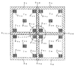
- FIG. 3 is an explanatory diagram when the transfer pattern of the phase shift mask is transferred four times to the resist film on the semiconductor wafer.
- the image I 1 is an image transferred when the transfer pattern of the phase shift mask is transferred once by exposure. The same applies to the images I 2 , I 3 , and I 4 .
- Image p 1a ⁇ p 1e is a pattern transferred on the same exposure and transfer the same image p 2a ⁇ p 2e, the image p 3a ⁇ p 3e, even image p 4a ⁇ p 4e.
- Images S 1 , S 2 , S 3 , and S 4 are images to which the light shielding band pattern of the phase shift mask is transferred. As shown in FIG.
- S 12 , S 13 , S 24 , and S 34 are areas where the transfer images of the two light-shielding bands are superimposed and transferred, and S 1234 is the image where the transfer images of the four light-shielding bands are superimposed and transferred. Area.
- the transfer pattern of the phase shift film can be arranged up to the vicinity of the light-shielding band (image S 1 ). It is increasing.
- the arrangement of the plurality of transfer patterns that are repeatedly transferred to the resist film on the semiconductor wafer has a positional relationship in which adjacent light-shielding band patterns overlap.
- the region where the light-shielding band pattern is overlapped and exposed and transferred is used as a cutting allowance when the chip is formed after each chip is formed on the semiconductor wafer.
- the phase shift film is often formed of a material containing silicon, and the light shielding film is formed of a material containing chromium (chromium-based material) having high etching selectivity with the phase shift film.
- the light shielding film made of a chromium-based material is patterned by dry etching using a mixed gas of chlorine-based gas and oxygen gas, but the resist film has low resistance to dry etching using a mixed gas of chlorine-based gas and oxygen gas. For this reason, when the thickness of the light shielding film is increased, the thickness of the resist film needs to be significantly increased. However, when a fine pattern is formed on such a resist film, problems such as collapse or missing of the resist pattern are likely to occur.
- Patent Document 2 it is possible to reduce the thickness of the resist film by providing a hard mask film made of a material containing silicon on a light shielding film made of a chromium-based material. .
- a light shielding film made of a chromium-based material is patterned by dry etching using a mixed gas of chlorine-based gas and oxygen gas, the etching tends to proceed toward the pattern side wall.
- dry etching using a hard mask film having a fine pattern as a mask is performed on the light shielding film, if the thickness of the light shielding film is large, the amount of side etching tends to increase, and the fineness formed on the light shielding film.
- the CD accuracy of the pattern tends to decrease.
- a decrease in CD accuracy of the fine pattern of the light shielding film leads to a decrease in CD accuracy of the fine pattern formed on the phase shift film by dry etching using the fine pattern of the light shielding film as a mask.
- a cleaning process is performed on the light-shielding film after patterning.
- the film thickness of the light-shielding film is large, there is a problem that the pattern of the light-shielding film tends to fall during the cleaning.
- the present invention is such that a phase shift film formed of a material containing silicon and a light shielding film including a layer formed of a material containing chromium are stacked in this order on a light-transmitting substrate.
- a mask blank having a structure a phase shift mask manufactured from the mask blank is set in an exposure apparatus of a complicated illumination system to which SMO is applied and provided on a semiconductor wafer or the like to be transferred. Even when the transferred resist film is exposed and transferred, the optical density higher than the conventional one is shielded from the phase shift film so that the fine pattern formed on the resist film after the development processing has high CD accuracy.
- a first object is to provide a mask blank having a laminated structure of films.
- the second object of the present invention is to provide a mask blank in which the CD accuracy of the fine pattern formed on the light shielding film by dry etching is high and the occurrence of the tilting of the light shielding film pattern is suppressed.
- the present invention also relates to a phase shift mask manufactured using this mask blank. Even when the phase shift mask is set in an exposure apparatus of a complicated illumination system and exposure transfer is performed on a resist film, the development is performed. It is possible to form a light-shielding band with a higher optical density than before so that the fine pattern formed on the resist film after processing has high CD accuracy, and it is possible to form a fine pattern with high precision on the phase shift film.
- An object of the present invention is to provide a simple phase shift mask.
- Another object of the present invention is to provide a semiconductor device manufacturing method using the phase shift mask.
- the present invention has the following configuration as means for solving the above problems.
- the optical density with respect to the exposure light of the ArF excimer laser in the laminated structure of the phase shift film and the light shielding film is 3.5 or more
- the light-shielding film has a structure in which a lower layer and an upper layer are laminated from the translucent substrate side,
- the lower layer is made of a material containing chromium and having a total content of chromium, oxygen, nitrogen and carbon of 90 atomic% or more
- the upper layer is made of a material containing metal and silicon, and the total content of metal and silicon is 80 atomic% or more,
- the upper layer the extinction coefficient k U with respect to the exposure light, the mask blank and greater than the extinction coefficient k L with respect to the lower layer of the exposure light.
- the optical density with respect to the exposure light of the ArF excimer laser in the laminated structure of the phase shift film and the light shielding film is 3.5 or more
- the light-shielding film has a structure in which a lower layer and an upper layer are laminated from the translucent substrate side,
- the lower layer is made of a material containing chromium and having a total content of chromium, oxygen, nitrogen and carbon of 90 atomic% or more
- the upper layer is made of a material containing metal and silicon, and the total content of metal and silicon is 80 atomic% or more,
- the upper layer the extinction coefficient k U with respect to the exposure light in a phase shift mask being larger than the extinction coefficient k L with respect to the lower layer of the exposure light.
- (Configuration 12) Refractive index n U with respect to the exposure light of the upper layer, the lower layer of the smaller than the refractive index n L with respect to the exposure light, the refractive index n of the refractive index n U with respect to the exposure light of the upper layer with respect to the exposure light of the lower layer phase shift mask according to any one of configurations 9, wherein 11 of the ratio n U / n L divided by L is 0.8 or more.
- the refractive index n L of the lower layer is 2.0 or less
- a phase shift mask according to the structure 12 refractive index n U of the upper layer is characterized in that less than 2.0.
- (Configuration 14) 14 14.
- the mask blank of the present invention Since the mask blank of the present invention has a high optical density suitable for SMO with an optical density of 3.5 or more with respect to the exposure light of the ArF excimer laser in the laminated structure of the phase shift film and the light shielding film, this mask blank is used. Even when the manufactured phase shift mask is set in an exposure apparatus of a complicated illumination system to which SMO is applied and exposure transfer is performed on a resist film to be transferred, the resist after development processing The CD accuracy of a fine pattern formed on the film can be increased.
- the mask blank of the present invention has a high CD accuracy of the formed fine pattern when the fine pattern is formed on the light shielding film by dry etching, and the fine pattern of the formed light shielding film falls down by washing or the like. Can be sufficiently suppressed.
- the phase shift mask of the present invention is manufactured using the mask blank of the present invention. Therefore, even when the phase shift mask is set in an exposure apparatus of a complicated illumination system to which SMO is applied and the exposure transfer is performed on the resist film of the transfer target, The CD accuracy of the fine pattern formed on the resist film can be increased. Moreover, since the phase shift mask of this invention manufactures a phase shift mask using the mask blank of this invention, a fine pattern can be accurately formed in a phase shift film. Furthermore, the semiconductor device manufacturing method using the phase shift mask of the present invention makes it possible to transfer a fine pattern to a resist film on a semiconductor wafer with good CD accuracy.
- the inventor sets a phase shift mask in an exposure apparatus of a complicated illumination system to which SMO is applied, and performs exposure transfer on a resist film provided on a semiconductor wafer or the like to be transferred.
- the optical density in the laminated structure of the phase shift film and the light-shielding film necessary for the fine pattern formed on the resist film after the development processing to have high CD accuracy was studied.
- an optical density (hereinafter simply referred to as optical density) with respect to ArF excimer laser exposure light (hereinafter referred to as ArF exposure light) in the laminated structure of the phase shift film and the light shielding film is required to be 3.5 or more. I found out.
- the transmittance of the phase shift film with respect to ArF exposure light is 6% (optical density is about 1.2), which is a widely used transmittance.
- the optical density of the light shielding film with respect to ArF exposure light needs to be 2.3 or more.
- the optical density was increased to 2.3 or more by increasing the thickness of the light-shielding film, it was necessary to significantly increase the thickness of the resist pattern, so that a fine pattern was formed on the light-shielding film by dry etching. It was difficult.
- a hard mask film made of a silicon-based material was provided on the light shielding film, and an attempt was made to form a fine pattern on the light shielding film by dry etching using the hard mask film on which the fine pattern was formed as a mask.
- the amount of side etching generated when a fine pattern is formed on the light shielding film is large, and the CD accuracy of the fine pattern formed on the light shielding film is lowered.
- the fine pattern is formed on the light shielding film and then washed, a phenomenon that the light shielding film pattern is detached occurs, and it is difficult to form the fine pattern on the light shielding film with this method. It was.
- a light-shielding film is formed with a material having an extremely high chromium content such that the optical density is 2.3 or more, a hard mask film of a silicon-based material is laminated on the light-shielding film, and a fine pattern is formed on the light-shielding film.
- this light-shielding film has a very slow etching rate for dry etching with a mixed gas of chlorine-based gas and oxygen gas, resulting in low CD uniformity in the plane of the pattern formed on the light-shielding film.
- the light shielding film a laminated structure of a lower layer of a chromium-based material and an upper layer of a metal silicide-based material.
- the lower layer of the light-shielding film By forming the lower layer of the light-shielding film on the phase shift film side with a chromium-based material, it has high etching resistance against dry etching with a fluorine-based gas performed when forming a fine pattern on the phase shift film. It can have a function as a hard mask.
- the phase shift film has high etching resistance against dry etching with a mixed gas of chlorine-based gas and oxygen gas, which is performed when removing the light shielding film, and therefore the influence on the phase shift film when removing the light shielding film.
- the upper layer of the light shielding film by forming the upper layer of the light shielding film with a metal silicide material, it has high etching resistance against dry etching with a mixed gas of chlorine gas and oxygen gas, which is performed when forming a fine pattern below the light shielding film. It can have a function as a hard mask.
- the upper layer of the light shielding film can be removed at the same time during dry etching with a fluorine-based gas performed when forming a fine pattern on the phase shift film.
- the lower layer of the light shielding film contains an element (such as silicon) that greatly reduces the etching rate with respect to dry etching with a mixed gas of chlorine-based gas and oxygen gas.
- the lower layer of the light-shielding film is made of a material containing chromium and having a total content of chromium, oxygen, nitrogen and carbon of 90 atomic% or more. From the above situation, it is difficult to increase the chromium content in the chromium-based material forming the lower layer of the light-shielding film, and the extinction coefficient k L for the lower ArF exposure light (hereinafter simply referred to as the extinction coefficient k L ).
- the upper layer of the light shielding film is often made of a material having a smaller extinction coefficient k than the lower layer in consideration of providing an antireflection function.
- recent improvements in the performance of exposure apparatuses have eased restrictions on surface reflectance in regions outside the transfer pattern region (including regions where light-shielding bands are formed). Therefore, we decided to such larger configurations also upper layer of the extinction coefficient k U lower layer of the extinction coefficient k L of the light-shielding film.
- the upper layer of the light shielding film is required to function as a hard mask when the lower layer of the chromium-based material is patterned by dry etching using a mixed gas of chlorine-based gas and oxygen gas.
- a conventional hard mask film made of a silicon-based material has been emphasized to improve etching selectivity with respect to a thin film of a chromium-based material, and a silicon material containing a relatively large amount of oxygen or nitrogen is used.
- the content of oxygen and nitrogen in the upper layer of the metal silicide material is lower than that of the conventional material, and etching for dry etching with a mixed gas of chlorine gas and oxygen gas between the lower layer of the chromium material. The selectivity was verified.
- the upper layer of the light-shielding film is made of a material containing metal and silicon, and the total content of metal and silicon is 80 atomic%.
- the mask blank of the present invention has been completed. Specifically, it is a mask blank having a structure in which a phase shift film and a light shielding film are laminated in this order on a translucent substrate, and the exposure light of the ArF excimer laser in the laminated structure of the phase shift film and the light shielding film.
- the optical density is 3.5 or more
- the light shielding film has a structure in which a lower layer and an upper layer are laminated from the translucent substrate side, the lower layer contains chromium, and the total content of chromium, oxygen, nitrogen, and carbon is
- the upper layer contains a metal and silicon, the total content of the metal and silicon is 80 atom% or more, and the extinction coefficient k U for the exposure light of the upper layer is: It is characterized by being larger than the extinction coefficient k L for the exposure light of the lower layer.
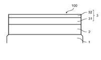
- FIG. 1 shows a schematic configuration of an embodiment of a mask blank.
- a mask blank 100 shown in FIG. 1 has a configuration in which a phase shift film 2, a lower layer 31 of a light shielding film 3, and an upper layer 32 of the light shielding film 3 are laminated in this order on one main surface of the translucent substrate 1.
- the mask blank 100 may have a configuration in which a resist film is laminated on the upper layer 32 as necessary.
- the mask blank 100 is at least required to have a laminated structure of the phase shift film 2 and the light shielding film 3 and have an optical density of 3.5 or more with respect to ArF exposure light.
- the mask blank 100 is a laminated structure of the phase shift film 2 and the light-shielding film 3, and the optical density with respect to ArF exposure light is more preferably 3.8 or more, and further preferably 4.0 or more.
- the optical density with respect to ArF exposure light is more preferably 3.8 or more, and further preferably 4.0 or more.
- the translucent substrate 1 is made of a material having good transparency to exposure light used in an exposure process in lithography.
- synthetic quartz glass, aluminosilicate glass, soda lime glass, low thermal expansion glass (such as SiO 2 —TiO 2 glass), and other various glass substrates can be used.
- a substrate using synthetic quartz glass has high transparency to ArF exposure light, it can be suitably used as the light-transmitting substrate 1 of the mask blank 100.
- the exposure process in lithography mentioned here is an exposure process in lithography performed using the phase shift mask produced using this mask blank 100, and exposure light is ArF used in this exposure process below.
- Excimer laser (wavelength: 193 nm).
- the phase shift film 2 transmits ArF exposure light with an intensity that does not substantially contribute to exposure, and exposure light that has passed through the air at the same distance as the thickness of the phase shift film 2 with respect to the transmitted ArF exposure light. Has a function of causing a predetermined phase difference between the two. Specifically, by patterning the phase shift film 2, a portion where the phase shift film 2 remains and a portion where the phase shift film 2 does not remain are formed, and the phase shift is applied to the exposure light transmitted through the portion where the phase shift film 2 is not present. The phase of the light transmitted through the film 2 (light with an intensity that does not substantially contribute to exposure) is substantially reversed.
- the phase shift film 2 has a transmittance with respect to ArF exposure light of preferably 1% or more, and more preferably 2% or more.
- the phase shift film 2 preferably has a transmittance with respect to ArF exposure light of 35% or less, and more preferably 30% or less.
- the phase shift film 2 preferably has the above phase difference of 150 degrees or more, and more preferably 160 degrees or more. Further, the phase shift film 2 preferably has a phase difference of 200 degrees or less, and more preferably 190 degrees or less.
- the phase shift film 2 is made of a material containing silicon (Si).
- the phase shift film 2 is preferably formed of a material containing nitrogen (N) in addition to silicon.
- Such a phase shift film 2 can be patterned by dry etching using a fluorine-based gas, and has sufficient etching selectivity with respect to a lower layer 31 of a Cr-based material constituting a light shielding film 3 described later.
- the phase shift film 2 is preferably formed of a material made of silicon and nitrogen, or a material containing one or more elements selected from a metalloid element and a nonmetal element in a material made of silicon and nitrogen.
- the phase shift film 2 may contain any metalloid element in addition to silicon and nitrogen. Among these metalloid elements, inclusion of one or more elements selected from boron (B), germanium (Ge), antimony (Sb), and tellurium (Te) can increase the conductivity of silicon used as a sputtering target. It is preferable because it can be expected.
- the phase shift film 2 may contain any nonmetallic element in addition to silicon and nitrogen.
- the nonmetallic element in the present invention includes a nonmetallic element in a narrow sense (nitrogen (N), carbon (C), oxygen (O), phosphorus (P), sulfur (S), selenium (Se)), halogen, and The thing containing noble gas.
- these nonmetallic elements it is preferable to include one or more elements selected from carbon, fluorine (F), and hydrogen (H).
- the phase shift film 2 may contain a noble gas (also referred to as a rare gas; hereinafter the same in this specification).
- the noble gas is an element that can increase the deposition rate and improve the productivity by being present in the deposition chamber when the phase shift film 2 is deposited by reactive sputtering.
- this noble gas is turned into plasma and collides with the target, the target constituent element pops out from the target and reaches the translucent substrate 1 while adhering to the translucent substrate 1 while taking in the reactive gas.
- a phase shift film 2 is formed on the conductive substrate 1.
- the noble gas in the film formation chamber is slightly taken in until the target constituent element jumps out of the target and adheres to the translucent substrate 1.
- Preferred examples of the noble gas required for this reactive sputtering include argon (Ar), krypton (Kr), and xenon (Xe).
- Ar argon
- Kr krypton
- Xe xenon
- helium (He) and neon (Ne) having a small atomic weight can be actively incorporated into the phase shift film.
- the phase shift film 2 may further contain a metal element as long as it can be patterned by dry etching using a fluorine-based gas.
- the metal elements to be contained are molybdenum (Mo), tungsten (W), titanium (Ti), tantalum (Ta), zirconium (Zr), hafnium (Hf), niobium (Nb), vanadium (V), cobalt (Co ), Chromium (Cr), nickel (Ni), ruthenium (Ru), tin (Sn), and aluminum (Al).
- the thickness of the phase shift film 2 is preferably 90 nm or less. If the thickness of the phase shift film 2 is greater than 90 nm, the time required for patterning by dry etching with a fluorine-based gas becomes longer.
- the phase shift film 2 is more preferably 80 nm or less in thickness.
- the phase shift film 2 preferably has a thickness of 40 nm or more. If the thickness of the phase shift film 2 is less than 40 nm, the predetermined transmittance and phase difference required for the phase shift film may not be obtained.
- the light shielding film 3 has a configuration in which a lower layer 31 and an upper layer 32 are laminated in this order from the phase shift film 2 side.
- the lower layer 31 contains chromium and is formed of a material having a total content of chromium, oxygen, nitrogen, and carbon of 90 atomic% or more.
- the lower layer 31 is preferably formed of a material having a total content of chromium, oxygen, nitrogen, and carbon of 95 atomic% or more, and more preferably formed of a material having 98 atomic% or more. This is because in order to increase the etching rate for dry etching using a mixed gas of chlorine-based gas and oxygen gas, it is preferable to reduce the content of elements other than the above (particularly silicon).
- the lower layer 31 may contain a metal element, a semi-metal element, and a non-metal element other than the above constituent elements as long as it satisfies the above-mentioned total content range.
- the metal element in this case include molybdenum, indium, and tin.
- the metalloid element in this case include boron and germanium.
- the nonmetallic element in this case include non-metallic elements in a narrow sense (phosphorus, sulfur, selenium), halogen (fluorine, chlorine, etc.), and noble gases (helium, neon, argon, krypton, xenon, etc.).
- the noble gas is an element that is slightly taken into the film when the lower layer 31 is formed by a sputtering method, and is also an element that may be beneficial if it is actively contained in the layer.
- content in the lower layer 31 is calculated
- the lower layer 31 is preferably formed of a material containing chromium and having a total content of chromium, oxygen, and carbon of 90 atomic% or more.
- the lower layer 31 is preferably formed of a material having a total content of chromium, oxygen and carbon of 95 atomic% or more, and more preferably formed of a material having 98 atomic% or more.
- the nitrogen content in the lower layer 31 increases, the etching rate for dry etching using a mixed gas of chlorine-based gas and oxygen gas increases, but the side etching amount also increases.
- the lower layer 31 preferably has a nitrogen content of less than 10 atomic%, more preferably 5 atomic% or less, and even more preferably 2 atomic% or less.
- the lower layer 31 is substantially composed of chromium, oxygen, and carbon, and includes an embodiment that does not substantially contain nitrogen.
- the lower layer 31 preferably has a chromium content of 50 atomic% or more.
- a material having a high optical density is selected for the upper layer 32, but it is preferable to secure a certain level of optical density for the lower layer 31. Another reason is to suppress side etching that occurs when the lower layer 31 is patterned by dry etching.
- the lower layer 31 preferably has a chromium content of 80 atomic% or less, and more preferably 75 atomic% or less. This is to ensure a sufficient etching rate when the light shielding film 3 is patterned by dry etching.
- the lower layer 31 preferably has an oxygen content of 10 atomic% or more, and more preferably 15 atomic% or more. This is to ensure a sufficient etching rate when the light shielding film 3 is patterned by dry etching.
- the lower layer 31 preferably has an oxygen content of 50 atomic% or less, more preferably 40 atomic% or less, and even more preferably 35 atomic% or less. This is because, similarly to the above, it is preferable to secure a certain optical density in the lower layer 31 as well. Another reason is to suppress side etching that occurs when the lower layer 31 is patterned by dry etching.
- the lower layer 31 preferably has a carbon content of 10 atomic% or more. This is to suppress side etching that occurs when the lower layer 31 is patterned by dry etching.
- the lower layer 31 preferably has a carbon content of 30 atomic% or less, more preferably 25 atomic% or less, and even more preferably 20 atomic% or less. This is to ensure a sufficient etching rate when the light shielding film 3 is patterned by dry etching.
- the lower layer 31 preferably has a difference in content of each element constituting the lower layer 31 in the film thickness direction of less than 10%. This is to reduce variations in the etching rate in the film thickness direction when the lower layer 31 is patterned by dry etching.
- the lower layer 31 preferably has a thickness larger than 15 nm, more preferably 18 nm or more, and further preferably 20 nm or more. On the other hand, the lower layer 31 preferably has a thickness of 60 nm or less, more preferably 50 nm or less, and further preferably 45 nm or less.
- a material having a high optical density is selected for the upper layer 32, but there is a limit to increasing the contribution of the upper layer 32 to the optical density required for the entire light shielding film 3. For this reason, it is necessary to ensure a certain optical density even in the lower layer 31.
- the lower layer 31 needs to increase the etching rate for dry etching using a mixed gas of chlorine-based gas and oxygen gas, there is a limit to improving the light shielding performance. Therefore, the lower layer 31 needs to have a predetermined thickness or more. On the other hand, if the lower layer 31 is too thick, it is difficult to suppress the occurrence of side etching. The range of the thickness of the lower layer 31 takes these restrictions into consideration.
- the upper layer 32 includes a metal and silicon, and is formed of a material having a total content of metal and silicon of 80 atomic% or more.
- the upper layer 32 is preferably formed of a material having a total content of metal and silicon of 85 atomic% or more, and more preferably formed of a material of 90 atomic% or more.
- metal and silicon are elements that enhance the light shielding performance of the upper layer 32 against ArF exposure light.
- high resistance to dry etching by a mixed gas of chlorine-based gas and oxygen gas which is performed when forming a fine pattern in the lower layer 31. It has been found that it can function as a hard mask.
- the upper layer 32 opposite to the phase shift film 2 is a surface that comes into contact with the atmosphere, the surface layer including the surface is likely to be oxidized. For this reason, it is difficult to form the entire upper layer 32 with only metal and silicon.
- the upper layer 32 has a higher light shielding performance than the lower layer 31.
- the upper layer 32 is required to be formed of a material having a total content of metal and silicon of 80 atomic% or more in the average of the entire layer, and is preferably 85 atomic% or more, More preferably, it is 90 atomic% or more.
- the metal elements contained in the upper layer 32 are molybdenum (Mo), tungsten (W), titanium (Ti), tantalum (Ta), zirconium (Zr), hafnium (Hf), niobium (Nb), vanadium (V), One or more metal elements from cobalt (Co), chromium (Cr), nickel (Ni), ruthenium (Ru), rhodium (Rh), palladium (Pd), indium (In), tin (Sn), and aluminum (Al) Is preferably selected.
- the metal element contained in the upper layer 32 is more preferably tantalum.
- Tantalum has a high atomic weight and high light shielding performance, and has a high resistance to a cleaning liquid used in a cleaning process performed in the course of manufacturing a phase shift mask from a mask blank and a cleaning liquid used in cleaning performed on a phase shift mask. It is.
- the upper layer 32 is preferably formed of a material having a total content of tantalum and silicon of 80 atomic% or more, more preferably 85 atomic% or more, and further preferably 90 atomic% or more.
- the upper layer 32 may contain a metalloid element and a nonmetal element other than the above constituent elements as long as the above total content range is satisfied.
- the metalloid element in this case include boron and germanium.
- Nonmetallic elements in this case include nonmetallic elements in a narrow sense (oxygen, nitrogen, carbon, phosphorus, sulfur, selenium), halogens (fluorine, chlorine, etc.), noble gases (helium, neon, argon, krypton, xenon, etc.) .
- the noble gas is an element that is slightly incorporated into the film when the upper layer 32 is formed by a sputtering method, and is also an element that may be beneficial when actively contained in the layer.
- the upper layer 32 is obtained by dividing the metal content [atomic%] by the total content of metal and silicon [atomic%] (that is, the total content [M + Si] [atomic%] of metal and silicon in the upper layer 32 is 100).
- the ratio of the metal content M [atomic%] when expressed as [%], hereinafter referred to as the M / [M + Si] ratio) is preferably 5% or more, and preferably 10% or more. And more preferably 15% or more.
- the upper layer 32 preferably has an M / [M + Si] ratio of 60% or less, more preferably 55% or less, and even more preferably 50% or less.
- a thin film of a metal silicide-based material has a tendency that the light shielding performance (optical density) increases as the content ratio of metal and silicon approaches a stoichiometrically stable ratio.
- the ratio is stoichiometrically stable when metal: silicon is 1: 2, and the M / [M + Si] ratio of the upper layer 32 takes the tendency into consideration. It is what.
- the thickness of the upper layer 32 is preferably 5 nm or more, more preferably 7 nm or more, and further preferably 10 nm or more. On the other hand, the thickness of the upper layer 32 is preferably 40 nm or less, more preferably 35 nm or less, and further preferably 30 nm or less.
- the contribution of the upper layer 32 to the optical density required for the entire light shielding film 3 needs to be higher than the contribution of the lower layer 31. Further, there is a limit to increasing the optical density per unit film thickness of the upper layer 32.
- the upper layer 32 since it is necessary for the upper layer 32 to be able to form a fine pattern by dry etching using a resist film having a fine pattern as a mask, there is a limit to increasing the thickness of the upper layer 32. .
- the thickness range of the upper layer 32 takes these restrictions into consideration.
- the upper layer 32 is preferably thinner than the lower layer 31.
- the upper layer 32 forms a fine pattern by dry etching using a resist film on which a fine pattern is formed as a mask, but the surface of the upper layer 32 tends to have low adhesion with a resist film made of an organic material. For this reason, it is preferable that the surface of the upper layer 32 is subjected to HMDS (Hexamethyldisilazane) treatment to improve surface adhesion.
- HMDS Hexamethyldisilazane
- the extinction coefficient k U of the upper layer 32 of the light shielding film 3 is required to be larger than the extinction coefficient k L of the lower layer 31.
- the extinction coefficient k L of the lower layer 31 is preferably 2.00 or less, more preferably 1.95 or less, and even more preferably 1.90 or less. Further, the extinction coefficient k L of the lower layer 31 is preferably 1.20 or more, more preferably 1.25 or more, and further preferably 1.30 or more. In contrast, the extinction coefficient k U of the upper layer 32 is preferably greater than 2.00, more preferable to be 2.10 or more and further preferably 2.20 or more. Further, the extinction coefficient k U of the upper layer 32 is preferably 3.20 or less, more preferable to be 3.10 or less, further preferably 3.00 or less.
- the phase shift film 2 needs to have both a function of transmitting exposure light that is transmitted with a predetermined transmittance and a function of generating a predetermined phase difference. Since the phase shift film 2 is required to realize these functions with a thinner film thickness, the phase shift film 2 is often formed of a material having a high refractive index n.
- the lower layer 31 of the light-shielding film 3 has a relatively high chromium content due to the above circumstances, and a low content of nitrogen, which is an element that tends to increase the refractive index n of the material when contained in the material. . For this reason, the lower layer 31 has a refractive index n smaller than that of the phase shift film 2.
- the upper layer 32 of the light-shielding film 3 is required to greatly improve the light-shielding performance as described above. From these circumstances, the mask blank 100 has a laminated structure in which the refractive index n decreases in the order of the phase shift film 2, the lower layer 31, and the upper layer 32.
- the exposure light traveling at a predetermined angle from the direction perpendicular to the interface of the phase shift film 2 enters the lower layer 31 of the light shielding film 3 from the phase shift film 2 with respect to the interface.
- the inclination angle from the vertical direction will increase. Furthermore, when the exposure light that has entered the lower layer 31 enters the upper layer 32, the inclination angle from the direction perpendicular to the interface is further expanded.
- the refractive index n U of the upper layer 32 is smaller than the refractive index n L of the lower layer 31 (i.e., the refractive index n U of the upper layer 32 in refractive index n L of the lower layer 31 less than divided by the ratio n U / n L is 1.0), the refractive index n U of the upper layer 32 the ratio n U / n L obtained by dividing the refractive index n L of the lower layer 31 is better to be a 0.8 or higher .
- the ratio n U / n L obtained by dividing the refractive index n U of the upper layer 32 by the refractive index n L of the lower layer 31 is more preferably 0.85 or more, and further preferably 0.9 or more.
- the refractive index n L of the lower layer 31 is preferably 2.00 or less, more preferably 1.98 or less, and even more preferably 1.95 or less. Further, the refractive index n L of the lower layer 31 is preferably 1.45 or more, more preferably 1.50 or more, and further preferably 1.55 or more. In contrast, the refractive index n U of the upper layer 32 is preferably less than 2.00, more preferable to be 1.95 or less, further preferably 1.90 or less. The refractive index n U of the upper layer 32 is preferably 1.30 or more, more preferably 1.35 or more and further preferably 1.40 or more.
- the surface reflectance of the exposure light on both main surfaces of the phase shift mask is not too high in order to prevent exposure transfer defects due to reflection of ArF exposure light.
- the reflectance on the surface side (surface farthest from the translucent substrate) of the light-shielding film, which receives the reflected light of the exposure light from the reduction optical system of the exposure apparatus is, for example, 60% or less (preferably 55%). It is desirable that This is to suppress stray light generated by multiple reflection between the surface of the light shielding film and the lens of the reduction optical system.
- the thickness of the light-shielding film 3 in the laminated structure of the lower layer 31 and the upper layer 32 is preferably 80 nm or less, more preferably 75 nm or less, and further preferably 70 nm or less. Further, the thickness of the light-shielding film 3 in the laminated structure of the lower layer 31 and the upper layer 32 is preferably 30 nm or more, more preferably 35 nm or more, and further preferably 40 nm or more. If the entire thickness of the light shielding film 3 is too thick, it is difficult to form a fine pattern on the light shielding film 3 with high accuracy. On the other hand, if the total thickness of the light shielding film 3 is too thin, it is difficult for the light shielding film 3 to satisfy the required optical density.
- the lower layer 31 and the upper layer 32 of the phase shift film 2 and the light shielding film 3 can be formed by sputtering.
- Sputtering may be performed using a direct current (DC) power source or a radio frequency (RF) power source, and may be a magnetron sputtering method or a conventional method.
- DC sputtering is preferred because the mechanism is simple.
- the film forming apparatus may be an in-line type or a single-wafer type.
- a resist film made of an organic material is preferably formed with a thickness of 100 nm or less in contact with the surface of the upper layer 32 of the light shielding film 3.
- the upper layer 32 is formed of a material capable of patterning a fine pattern by dry etching with fluorine gas. Since the upper layer 32 functions as a hard mask at the time of dry etching with a mixed gas of chlorine-based gas and oxygen gas, which is performed when patterning a fine pattern on the lower layer 31, the light shielding film 3 even if the resist film is 100 nm or less. It is possible to form a fine pattern. More preferably, the resist film has a thickness of 80 nm or less.
- the resist film is preferably a resist for electron beam drawing exposure, and more preferably, the resist is a chemical amplification type.
- the mask blank 100 as described above has a high optical density suitable for SMO having an optical density of 3.5 or more with respect to the exposure light of the ArF excimer laser in the laminated structure of the phase shift film 2 and the light shielding film 3. For this reason, when a phase shift mask manufactured from the mask blank 100 is set in an exposure apparatus of a complicated illumination system to which SMO is applied, and exposure transfer is performed on a resist film to be transferred. In addition, the CD accuracy of the fine pattern formed on the resist film after the development process can be increased. Further, when a fine pattern is formed on the light shielding film 3 by dry etching, the mask blank 100 has a high CD accuracy of the formed fine pattern, and the formed fine pattern of the light shielding film 3 is tilted by cleaning or the like. Can be sufficiently suppressed.
- the mask blank 100 having the above configuration is manufactured by the following procedure.
- the translucent substrate 1 is prepared.
- the translucent substrate 1 has its end face and main surface polished to a predetermined surface roughness (for example, a root mean square roughness Rq of 0.2 nm or less in a square inner region having a side of 1 ⁇ m), and then a predetermined surface roughness.
- a predetermined surface roughness for example, a root mean square roughness Rq of 0.2 nm or less in a square inner region having a side of 1 ⁇ m
- a phase shift film 2 is formed on the translucent substrate 1 by a sputtering method. After the phase shift film 2 is formed, an annealing process at a predetermined heating temperature is performed as a post process. Next, the lower layer 31 of the light shielding film 3 is formed on the phase shift film 2 by sputtering. Then, the upper layer 32 is formed on the lower layer 31 by sputtering. In the formation of each layer by sputtering, a sputtering target and a sputtering gas containing the material constituting each layer in a predetermined composition ratio are used, and if necessary, a mixed gas of the above-mentioned noble gas and reactive gas is sputtered. Film formation using gas is performed.
- the mask blank 100 has a resist film
- the surface of the upper layer 32 is subjected to HMDS treatment as necessary.
- a resist film is formed on the surface of the upper layer 32 that has been subjected to the HMDS process by a coating method such as a spin coating method, and the mask blank 100 is completed.
- HMDS treatment is performed on the surface of the upper layer 32 of the light shielding film 3 in the mask blank 100.
- a resist film is formed on the upper layer 32 after the HMDS treatment by a spin coating method.
- a first pattern (phase shift pattern, transfer pattern) to be formed on the phase shift film 2 is exposed and drawn on the resist film with an electron beam.
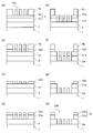
- the resist film is subjected to predetermined processing such as PEB (post-exposure baking) processing, development processing, post-baking processing, and the like to form a first pattern (phase shift pattern) (resist pattern 4a) on the resist film ( (See FIG. 2 (a)).
- PEB post-exposure baking
- the upper layer 32 of the light shielding film 3 is dry-etched using a fluorine-based gas to form a first pattern (upper layer pattern 32a) on the upper layer 32 (see FIG. 2B). ). Thereafter, the resist pattern 4a is removed (see FIG. 2C).
- dry etching of the lower layer 31 of the light-shielding film 3 may be performed with the resist pattern 4a remaining without being removed. In this case, the resist pattern 4a disappears when the lower layer 31 is dry etched.
- the dry etching for the lower layer 31 uses an etching gas having a higher mixing ratio of chlorine-based gas than conventional.
- the anisotropy of dry etching can be increased.
- the bias voltage applied from the back side of the translucent substrate 1 is also made higher than before.
- the power when applying this bias voltage is preferably 15 [W] or more, more preferably 20 [W] or more, and 30 [W] or more is more preferable.
- a resist film is formed on the upper layer pattern 32a and the phase shift film 2 by a spin coating method.
- a second pattern (a pattern including a light shielding band pattern) to be formed on the light shielding film 3 is exposed and drawn on the resist film with an electron beam.
- a predetermined process such as a development process is performed to form a resist film having a second pattern (light-shielding pattern) (resist pattern 5b) (see FIG. 2E).
- etching using a fluorine-based gas is performed to form a first pattern (phase shift pattern 2a) on the phase shift film 2 using the lower layer pattern 31a as a mask, and to the upper layer pattern 32a using the resist pattern 5b as a mask.
- a second pattern (upper layer pattern 32b) is formed (see FIG. 2F).
- the resist pattern 5b is removed.
- a second pattern (lower layer pattern 31b) in the lower layer pattern 31a (FIG. 2G). (See (h)).
- the dry etching of the lower layer pattern 31a may be performed under the conventional conditions of the mixing ratio of the chlorine-based gas and the oxygen gas and the bias voltage.
- a phase shift mask 200 is obtained through a predetermined process such as cleaning (see FIG. 2H).
- the chlorine-based gas used in the dry etching during the manufacturing process is not particularly limited as long as it contains Cl.
- a chlorine-based gas Cl 2, SiH 2 Cl 2 , CHCl 3, CH 2 Cl 2, CCl 4, BCl 3 and the like.
- the fluorine-based gas used in the dry etching in the manufacturing process is not particularly limited as long as F is contained.
- a fluorine-based gas CHF 3, CF 4, C 2 F 6, C 4 F 8, SF 6 and the like.
- the fluorine-based gas not containing C has a relatively low etching rate with respect to the glass substrate, damage to the glass substrate can be further reduced.
- the phase shift film (phase shift pattern 2a) having a transfer pattern and the light shielding film (light shielding pattern 3b) having a light shielding pattern are arranged in this order on the translucent substrate 1. It has a laminated structure (see FIG. 2 (h)). Since this phase shift mask is manufactured from the mask blank 100, it has the same characteristics as the mask blank 100. That is, the phase shift mask 200 is a phase shift mask having a structure in which a phase shift film 2 having a transfer pattern and a light shielding film 3 having a light shielding band pattern are laminated in this order on a light transmitting substrate 1.
- the optical density of the ArF excimer laser with respect to the exposure light in the laminated structure of the shift film 2 and the light shielding film 3 is 3.5 or more, and the light shielding film 3 is formed by laminating the lower layer 31 and the upper layer 32 from the translucent substrate 1 side.
- the lower layer 31 is made of a material containing chromium and having a total content of chromium, oxygen, nitrogen and carbon of 90 atomic% or more, and the upper layer 32 contains metal and silicon. It consists total content is 80 atomic% or more materials, the extinction coefficient k U with respect to the exposure light of the upper layer 32, especially greater than the extinction coefficient k L with respect to the exposure light of the lower layer 31 It is set to.
- This phase shift mask 200 is manufactured using the mask blank 100. For this reason, this phase shift mask 200 is set in an exposure apparatus of a complicated illumination system to which SMO is applied, and development processing is performed even when exposure transfer is performed on a resist film to be transferred. The CD accuracy of a fine pattern formed on the subsequent resist film can be increased.
- phase shift pattern 2a the transfer pattern of the phase shift mask 200 is exposed and transferred to the resist film on the semiconductor substrate using the phase shift mask 200 described above.
- the manufacturing method of such a semiconductor device is performed as follows.
- a substrate for forming a semiconductor device is prepared.
- This substrate may be, for example, a semiconductor substrate, a substrate having a semiconductor thin film, or a microfabricated film formed thereon.
- a resist film is formed on the prepared substrate, and the resist film is repeatedly subjected to reduced transfer exposure using the phase shift mask 200 described above. Thereby, the transfer pattern formed on the phase shift mask 200 is arranged without a gap with respect to the resist film.
- the exposure apparatus used at this time is capable of irradiating ArF exposure light with an optimal illumination system to the phase shift mask 200 to which the phase shift pattern 2a is optimized by applying SMO.
- the resist film to which the transfer pattern is exposed and transferred is developed to form a resist pattern, the surface pattern of the substrate is etched using this resist pattern as a mask, and impurities are introduced. . After the processing is completed, the resist pattern is removed.
- the semiconductor device is completed by repeatedly performing the above processing on the substrate while exchanging the transfer mask, and further performing necessary processing.
- an exposure apparatus that can irradiate ArF exposure light with a complex but optimal illumination system is applied to the phase shift mask 200 to which the phase shift pattern 2a is optimized by applying SMO.
- the phase shift mask 200 has an optical density with respect to ArF exposure light of 3.5 or more, which is significantly higher than the conventional one, in the laminated structure of the phase shift pattern 2a and the light shielding pattern 3b constituting the light shielding band.
- extinction coefficient k U of upper layer pattern 32b and 3b are larger than the extinction coefficient k L of the lower layer pattern 31b, and has a so as to sufficiently suppress constituting the leakage light from the light-shielding band.
- the extinction coefficient k U of upper layer pattern 32b and 3b are larger than the extinction coefficient k L of the lower layer pattern 31b, and has a so as to sufficiently suppress constituting the leakage light from the light-shielding band.
- Example 1 Manufacture of mask blanks
- a translucent substrate 1 made of synthetic quartz glass having a main surface dimension of about 152 mm ⁇ about 152 mm and a thickness of about 6.35 mm was prepared.
- the translucent substrate 1 has its end face and main surface polished to a predetermined surface roughness (root mean square roughness Rq of 0.2 nm or less), and then subjected to a predetermined cleaning process and drying process.
- Argon (Ar), nitrogen (N 2 ), and helium (He) mixed gas as a sputtering gas by reactive sputtering (DC sputtering), a phase shift made of molybdenum, silicon, and nitrogen on the light-transmitting substrate 1 Film 2 was formed with a thickness of 69 nm.
- a heat treatment for reducing the film stress of the phase shift film 2 and forming an oxide layer on the surface layer was performed on the translucent substrate 1 on which the phase shift film 2 was formed.
- a heating furnace electric furnace
- heat treatment was performed in the atmosphere at a heating temperature of 450 ° C. and a heating time of 1 hour.
- a phase shift amount measuring apparatus MPM193, manufactured by Lasertec Corporation
- the transmittance and phase difference of the phase shift film 2 after the heat treatment with respect to light having a wavelength of 193 nm were measured. As a result, the transmittance was 6.0% and the phase difference was It was 177.0 degrees (deg).
- phase shift film 2 is formed in the DC sputtering apparatus, using a chromium (Cr) target, an argon (Ar), carbon dioxide (CO 2) and helium Reactive sputtering (DC sputtering) was performed in a mixed gas atmosphere of (He).
- a chromium (Cr) target an argon (Ar), carbon dioxide (CO 2) and helium Reactive sputtering (DC sputtering) was performed in a mixed gas atmosphere of (He).
- the lower layer 31 of the light-shielding film (CrOC film) 3 made of chromium, oxygen and carbon was formed in a thickness of 43 nm in contact with the phase shift film 2.
- the translucent substrate 1 in which the phase shift film 2 and the lower layer 31 are laminated is placed in a single wafer DC sputtering apparatus, and a tantalum silicide (TaSi 2 ) target is used and argon (Ar) gas is sputtered.
- the upper layer 32 of the light shielding film 3 made of tantalum and silicon was formed to a thickness of 8 nm on the lower layer 31 of the light shielding film 3 by DC sputtering.
- the light-transmitting substrate 1 on which the lower layer (CrOC film) 31 and the upper layer (TaSi film) 32 were formed was subjected to heat treatment. Specifically, using a hot plate, heat treatment was performed in the atmosphere at a heating temperature of 280 ° C. and a heating time of 5 minutes. After the heat treatment, an ArF excimer having a laminated structure of the phase shift film 2 and the light-shielding film 3 is used for the translucent substrate 1 on which the phase shift film 2 and the light-shielding film 3 are laminated, using a spectrophotometer (Cary 4000 manufactured by Agilent Technologies) The optical density at the wavelength of the laser beam (about 193 nm) was measured and found to be 4.12. Further, the surface reflectance of the light shielding film 3 opposite to the phase shift film 2 was measured and found to be 51%. Finally, a predetermined cleaning process was performed to manufacture the mask blank 100 of Example 1.
- a spectrophotometer Cary 4000 manufactured by Agilent Technologies
- phase shift film 2 and the light shielding film 3 were laminated on the main surface of another translucent substrate 1 under the same conditions.
- the phase shift film 2 and the light shielding film 3 of this mask blank were analyzed by X-ray photoelectron spectroscopy (XPS) (with RBS correction).
- XPS X-ray photoelectron spectroscopy
- the composition of the inner region excluding the surface layer (region from the surface opposite to the translucent substrate 1 to a depth of 3 nm) where oxidation of the phase shift film 2 proceeds is Mo: 6 atomic%, Si : 45 atomic%, N: 49 atomic%.
- the composition of the lower layer 31 of the light-shielding film 3 is Cr: 71 atomic%, O: 15 atomic%, C: 14 atomic%, and the upper layer 32 is oxidized (opposite to the translucent substrate 1).
- the composition of the inner region excluding the region from the side surface to a depth of 3 nm was Ta: 32 atomic% and Si: 68 atomic%.
- the difference between the constituent elements in the thickness direction was 3 atomic% or less, and it was confirmed that there was substantially no composition gradient in the thickness direction.
- the difference of each constituent element in the thickness direction in the inner region of the upper layer 32 was 3 atomic% or less, and it was confirmed that there was substantially no composition gradient in the thickness direction in the inner region.
- the total content of tantalum (Ta) and silicon (Si) in the entire upper layer 32 was 80 atomic% or more.
- the refractive index n and the extinction coefficient k for light having a wavelength of 193 nm in the lower layer 31 and the upper layer 32 of the light shielding film 3 were measured using a spectroscopic ellipsometer (M-2000D manufactured by JA Woollam).
- M-2000D manufactured by JA Woollam
- the refractive index n L at the wavelength 193 nm of the lower layer 31 is 1.82 and the extinction coefficient k L is 1.83
- the refractive index n U at the wavelength 193 nm of the upper layer 32 is 1.78
- the extinction coefficient k U. was 2.84.
- the ratio n U / n L obtained by dividing the refractive index n U of the upper layer 32 at a wavelength of 193 nm by the refractive index n L of the lower layer 31 at a wavelength of 193 nm was 0.978.
- the halftone phase shift mask 200 of Example 1 was manufactured by the following procedure. First, the surface of the upper layer 32 of the light shielding film 3 was subjected to HMDS treatment. Subsequently, a resist film made of a chemically amplified resist for electron beam drawing was formed with a film thickness of 100 nm in contact with the surface of the upper layer 32 by spin coating. Next, a first pattern which is a phase shift pattern to be formed on the phase shift film 2 is drawn on the resist film by electron beam, a predetermined development process and a cleaning process are performed, and the resist having the first pattern A pattern 4a was formed (see FIG. 2A). The first pattern drawn by exposure was optimized by applying SMO. Further, the first pattern has a fine pattern in the vicinity of the light shielding band, as indicated by p 1a to p 1d in FIG.
- a resist film was formed on the upper layer pattern 32a and the phase shift film 2 by a spin coating method.
- a second pattern (a pattern including a light shielding band pattern) to be formed on the light shielding film 3 was exposed and drawn with an electron beam on the resist film.
- predetermined processing such as development processing was performed to form a resist film (resist pattern 5b) having a second pattern (light-shielding pattern) (see FIG. 2E).
- phase shift mask 200 of Example 1 was subjected to mask inspection using a mask inspection apparatus (Teron 600 Series manufactured by KLA-Tencor), no defects were found in the phase shift pattern 2a. From this, it was confirmed that even the light-shielding film 3 having higher light-shielding performance than the conventional one sufficiently functions as a hard mask for forming the fine pattern of the resist pattern 4a on the phase shift film 2. Further, even if the total content of metal and silicon in the upper layer 32 is increased, it has high resistance to dry etching with a mixed gas of chlorine-based gas and oxygen gas that is performed when forming a fine pattern in the lower layer 31; It was confirmed that it functions as a hard mask.
- the CD accuracy of the fine pattern formed on the phase shift film 2 is lowered, and the CD accuracy of the fine pattern formed on the phase shift film 2 has been concerned about the light shielding film 3 having higher light shielding performance than before. It has been confirmed that the problem of deterioration of the light shielding film and the occurrence of pattern collapse of the light shielding film 3 are not a problem at all, the CD accuracy of these fine patterns is high, and the occurrence of pattern collapse of the light shielding film 3 can be suppressed. .
- the phase shift mask 200 of Example 1 is set on a mask stage of an exposure apparatus that can irradiate the phase shift mask 200 with ArF exposure light with an illumination system optimized by SMO, and a resist on a semiconductor substrate.
- the film was repeatedly exposed and transferred in the arrangement as shown in FIG.
- the resist film on the semiconductor substrate after exposure and transfer was subjected to development processing and the like to form a resist pattern.
- the resist pattern was observed by SEM, it was confirmed that the resist pattern was formed with high CD accuracy.
- the fine patterns p 1d , p 2c , p 3b , and p 4a in the vicinity of the image S 1234 in the region where the shading band shown in FIG. It was confirmed that it was formed. From this result, it can be said that the circuit pattern can be formed with high accuracy by dry etching using the resist pattern as a mask.
- Example 2 Manufacture of mask blanks
- the mask blank 100 of Example 2 was manufactured in the same procedure as in Example 1 except that the lower layer 31 of the light shielding film 3 was formed with a thickness of 18 nm and the upper layer 32 was formed with a thickness of 24 nm.
- a spectrophotometer Cary 4000 manufactured by Agilent Technologies
- the optical density at the wavelength of light (about 193 nm) of an ArF excimer laser having a laminated structure of the phase shift film 2 and the light shielding film 3. was 412.
- the surface reflectance of the light shielding film 3 on the side opposite to the phase shift film 2 was measured and found to be 55%.
- phase shift mask 200 of Example 2 was manufactured in the same procedure as in Example 1.
- the phase shift mask 200 of the second embodiment is subjected to mask inspection with a mask inspection apparatus (Teron600 Series manufactured by KLA-Tencor), and no defect is found in the phase shift pattern 2a. It was. From this, the same thing as Example 1 has been confirmed.
- the phase shift mask 200 of the second embodiment is applied to the mask stage of the exposure apparatus that can irradiate the phase shift mask 200 with ArF exposure light with an illumination system optimized by SMO.
- the resist film on the semiconductor substrate was repeatedly exposed and transferred in an arrangement as shown in FIG.
- the resist film on the semiconductor substrate after exposure and transfer was subjected to development processing and the like to form a resist pattern.
- the resist pattern was observed by SEM, it was confirmed that the resist pattern was formed with high CD accuracy.
- the fine patterns p 1d , p 2c , p 3b , and p 4a in the vicinity of the image S 1234 in the region where the shading band shown in FIG. It was confirmed that it was formed. From this result, it can be said that the circuit pattern can be formed with high accuracy by dry etching using the resist pattern as a mask.
- Example 3 Manufacture of mask blanks
- the mask blank 100 of Example 3 was manufactured in the same procedure as Example 1 except for the light shielding film 3.
- the lower layer 32 is formed of a CrOCN film, and the thickness of the upper layer 31 is changed with the same composition as that of Example 1.
- the translucent substrate 1 on which the phase shift film 2 is formed is installed in a single-wafer DC sputtering apparatus, and using a chromium (Cr) target, argon (Ar), carbon dioxide (CO 2 ).
- Reactive sputtering (DC sputtering) in a mixed gas atmosphere of nitrogen (N 2 ) and helium (He) was performed.
- the lower layer 31 of the light shielding film (CrOCN film) 3 made of chromium, oxygen, carbon and nitrogen was formed in a thickness of 43 nm in contact with the phase shift film 2.
- the translucent substrate 1 in which the phase shift film 2 and the lower layer 31 are laminated is placed in a single wafer DC sputtering apparatus, and a tantalum silicide (TaSi 2 ) target is used and argon (Ar) gas is sputtered.
- the upper layer 32 of the light shielding film 3 made of tantalum and silicon was formed to a thickness of 12 nm on the lower layer 31 of the light shielding film 3 by DC sputtering.
- Example 1 a mask blank in which the phase shift film 2 and the light shielding film 3 were laminated on the main surface of another translucent substrate 1 under the same conditions was manufactured.
- the lower layer 31 and the upper layer 32 of the mask blank of Example 3 were analyzed by X-ray photoelectron spectroscopy (with XPS and RBS correction).
- the composition of the lower layer 31 was Cr: 55 atomic%, O: 22 atomic%, C: 12 atomic%, and N: 11 atomic%.
- the difference of each constituent element in the thickness direction in the inner region of the lower layer 31 was 3 atomic% or less, and it was confirmed that there was substantially no composition gradient in the thickness direction in the inner region.
- the upper layer 32 was almost the same as the upper layer 32 of Example 1.
- the refractive index n and the extinction coefficient k for light having a wavelength of 193 nm in the lower layer 31 of the mask blank of Example 3 were measured using a spectroscopic ellipsometer (M-2000D manufactured by JA Woollam).
- M-2000D manufactured by JA Woollam
- the refractive index n L of the lower layer 31 at a wavelength of 193 nm was 1.93
- the extinction coefficient k L was 1.50.
- the upper layer 32 was almost the same as the upper layer of Example 1.
- the ratio n U / n L obtained by dividing the refractive index n U of the upper layer 32 at a wavelength of 193 nm by the refractive index n L of the lower layer 31 at a wavelength of 193 nm was 0.922.
- the optical density at the wavelength of light (about 193 nm) of the ArF excimer laser having the laminated structure of the phase shift film 2 and the light shielding film 3 was measured. It was 4.06 when measured. Further, the surface reflectance of the light shielding film 3 on the side opposite to the phase shift film 2 was measured and found to be 52%.
- phase shift mask 200 of Example 3 was manufactured in the same procedure as in Example 1.
- the phase shift mask 200 of the third embodiment is subjected to mask inspection with a mask inspection apparatus (Teron 600 Series manufactured by KLA-Tencor), and no defect is found in the phase shift pattern 2a. It was. From this, the same thing as Example 1 has been confirmed.
- the phase shift mask 200 of the third embodiment is applied to a mask stage of an exposure apparatus that can irradiate the phase shift mask 200 with ArF exposure light by an illumination system optimized by SMO.
- the resist film on the semiconductor substrate was repeatedly exposed and transferred in an arrangement as shown in FIG.
- the resist film on the semiconductor substrate after exposure and transfer was subjected to development processing and the like to form a resist pattern.
- the resist pattern was observed by SEM, it was confirmed that the resist pattern was formed with high CD accuracy.
- the fine patterns p 1d , p 2c , p 3b , and p 4a in the vicinity of the image S 1234 in the region where the shading band shown in FIG. It was confirmed that it was formed. From this result, it can be said that the circuit pattern can be formed with high accuracy by dry etching using the resist film as a mask.
- Comparative Example 1 Manufacture of mask blanks
- the mask blank of Comparative Example 1 was manufactured in the same procedure as in Example 1 except for the light shielding film 3.
- the lower layer is formed of a CrOCN film and the upper layer is formed of a SiO 2 film.
- a translucent substrate on which a phase shift film is formed is installed in a single-wafer DC sputtering apparatus, and using a chromium (Cr) target, argon (Ar), carbon dioxide (CO 2 ), nitrogen Reactive sputtering (DC sputtering) was performed in a mixed gas atmosphere of (N 2 ) and helium (He).
- Cr chromium
- Ar argon
- CO 2 carbon dioxide
- DC sputtering nitrogen Reactive sputtering
- a lower layer of a light shielding film (CrOCN film) made of chromium, oxygen, and carbon was formed in a thickness of 43 nm in contact with the phase shift film.
- a translucent substrate in which a lower layer of a phase shift film and a light shielding film is stacked is installed in a single wafer RF sputtering apparatus, and a silicon dioxide (SiO 2 ) target is used, and argon (Ar) gas is sputtered.
- the upper layer of the light shielding film made of silicon and oxygen was formed to a thickness of 12 nm on the lower layer of the light shielding film by RF sputtering.
- Example 2 In the same manner as in Example 1, a mask blank in which a phase shift film and a light-shielding film were laminated on the main surface of another translucent substrate under the same conditions was manufactured.
- the lower layer and the upper layer of the light shielding film of the mask blank in Comparative Example 1 were analyzed by X-ray photoelectron spectroscopy (with XPS and RBS correction).
- the composition of the lower layer is Cr: 55 atomic%, O: 22 atomic%, C: 12 atomic%, N: 11 atomic%
- the composition of the upper layer is Si: 35 atomic%, O: 65 atomic% Met.
- the difference of each constituent element in the thickness direction in the inner region of the lower layer and the upper layer was 3 atomic% or less, and it was confirmed that there was substantially no composition gradient in the thickness direction in the inner region.
- the refractive index n and extinction coefficient k for light having a wavelength of 193 nm in the lower layer of the mask blank of Comparative Example 1 were measured using a spectroscopic ellipsometer (M-2000D manufactured by JA Woollam). did.
- the refractive index n L at the lower layer wavelength of 193 nm was 1.93, and the extinction coefficient k L was 1.50.
- the refractive index n U in the upper layer of the wavelength of 193nm is 1.59, extinction coefficient k U was 0.00.
- the ratio n U / n L obtained by dividing the refractive index n U of the upper layer 32 at a wavelength of 193 nm by the refractive index n L of the lower layer 31 at a wavelength of 193 nm was 0.824.
- an optical density at a wavelength of light (about 193 nm) of an ArF excimer laser having a laminated structure of a phase shift film and a light shielding film was measured using a spectrophotometer (Cary4000 manufactured by Agilent Technologies). However, it was 3.01. Further, when the surface reflectance of the light shielding film on the side opposite to the phase shift film was measured, it was 11%.
- the phase shift mask 200 of Comparative Example 1 was manufactured in the same procedure as in Example 1.
- a mask inspection was performed on the phase shift mask of Comparative Example 1 using a mask inspection apparatus (Teron600 Series manufactured by KLA-Tencor)
- no defects were found in the phase shift pattern 2a.
- the light-shielding film 3 having the same light-shielding performance thickness is also equivalent to the conventional one
- the light-shielding performance is not increased by the composition, and the optical density is not secured by increasing the thickness. It was confirmed that it sufficiently functions as a hard mask for forming the fine pattern of the resist pattern 4a on the phase shift film.
- the phase shift mask of the first comparative example is applied to the mask stage of the exposure apparatus that can irradiate the phase shift mask 200 with ArF exposure light with an illumination system optimized by SMO.
- the resist film on the semiconductor substrate was set and repeatedly exposed and transferred in an arrangement as shown in FIG.
- the resist film on the semiconductor substrate after exposure and transfer was subjected to development processing and the like to form a resist pattern.
- the fine pattern p 1d , p 2c , p 3b in the vicinity of the image S 1234 in the region where the shading band shown in FIG. , P 4a was found to have particularly low CD accuracy. From this result, it can be said that when a circuit pattern is formed by dry etching using this resist film as a mask, a circuit defect or the like may occur.
- Phase shift film 2a Phase shift pattern 3 Light shielding film 31 Lower layer 32 Upper layer 3b Light shielding pattern 31a, 31b Lower layer pattern 32a, 32b Upper layer pattern 4a, 5b Resist pattern 100 Mask blank 200 Phase shift mask
Landscapes
- Physics & Mathematics (AREA)
- General Physics & Mathematics (AREA)
- Preparing Plates And Mask In Photomechanical Process (AREA)
- Physical Vapour Deposition (AREA)
- Exposure And Positioning Against Photoresist Photosensitive Materials (AREA)
- Thin Film Transistor (AREA)
Abstract
マスクブランク(100)は、透光性基板(1)上に、位相シフト膜(2)と遮光膜(3)がこの順に積層した構造を備える。位相シフト膜と遮光膜の積層構造でのArFエキシマレーザーの露光光に対する光学濃度は3.5以上であり、遮光膜は、透光性基板側から下層(31)および上層(32)が積層した構造を備える。下層は、クロム、酸素、窒素および炭素の合計含有量が90原子%以上である材料からなり、上層は、金属およびケイ素の合計含有量が80原子%以上である材料からなる。上層の露光光に対する消衰係数kUは、下層の露光光に対する消衰係数kLよりも大きい。
Description
本発明は、位相シフトマスク用のマスクブランク、位相シフトマスク及びこの位相シフトマスクを用いる半導体デバイスの製造方法に関する。
一般に、半導体デバイスの製造工程では、フォトリソグラフィー法を用いて微細パターンの形成が行われている。この微細パターンの形成には、通常何枚もの転写用マスクと呼ばれている基板が使用される。この転写用マスクは、一般に透光性のガラス基板上に、金属薄膜等からなる微細パターンを設けたものである。この転写用マスクの製造においてもフォトリソグラフィー法が用いられている。
転写用マスクの種類としては、従来の透光性基板上にクロム系材料からなる遮光膜パターンを備えたバイナリマスクの他に、ハーフトーン型位相シフトマスクが知られている。このハーフトーン型位相シフトマスクは、透光性基板上に位相シフト膜のパターンを備えたものである。この位相シフト膜は、実質的に露光に寄与しない強度で光を透過させ、かつその位相シフト膜を透過した光に、同じ距離だけ空気中を通過した光に対して所定の位相差を生じさせる機能を有しており、これにより、いわゆる位相シフト効果を生じさせている。
特許文献1に開示されているように、露光装置を用いて転写用マスクのパターンを1枚の半導体ウェハ上のレジスト膜に露光転写を行う場合、その転写用マスクのパターンをそのレジスト膜の異なる位置に繰り返し露光転写を行うのが一般的である。また、そのレジスト膜への繰り返し露光転写は、間隔を置かずに行われる。露光装置には、転写用マスクの転写パターンが形成されている領域(転写領域)だけに露光光が照射されるようにアパーチャーが設けられている。しかし、アパーチャーによって露光光を被覆(遮蔽)する精度には限界があり、転写用マスクの転写領域よりも外側に露光光が漏れてしまうことは避け難い。このため、転写用マスクにおける転写パターンが形成される領域の外周領域は、露光装置を用いて半導体ウェハ上のレジスト膜に露光転写した際に、上記外周領域を透過した露光光による影響をレジスト膜が受けないように、所定値以上の光学濃度(OD:Optical Dimension)を確保することが求められている。通常、転写用マスクの外周領域では、ODが3以上(透過率 約0.1%以下)であると望ましいとされており、少なくとも2.8程度(透過率 約0.16%)は必要とされている。
しかし、ハーフトーン型位相シフトマスクの位相シフト膜は、露光光を所定の透過率で透過させる機能を有しており、この位相シフト膜だけでは、転写用マスクの外周領域に求められている光学濃度を確保することが困難である。このため、特許文献1に開示されているように、ハーフトーン型位相シフトマスクの場合、外周領域の光半透光層の上に遮光層(遮光帯)を積層することで、光半透光層と遮光層の積層構造で上記の所定値以上の光学濃度を確保することが行われている。
一方、特許文献2に開示されているように、ハーフトーン型位相シフトマスクのマスクブランクとして、透光性基板上に金属シリサイド系材料からなるハーフトーン位相シフト膜、クロム系材料からなる遮光膜、無機系材料からなるエッチングマスク膜が積層した構造を有するマスクブランクが以前より知られている。このマスクブランクを用いて位相シフトマスクを製造する場合、先ず、マスクブランクの表面に形成したレジストパターンをマスクとしてフッ素系ガスによるドライエッチングでエッチングマスク膜をパターニングする。次に、エッチングマスク膜パターンをマスクとして塩素と酸素の混合ガスによるドライエッチングで遮光膜をパターニングし、さらに遮光膜パターンをマスクとしてフッ素系ガスによるドライエッチングで位相シフト膜をパターニングする。
近年、ArFエキシマレーザ(波長193nm)を露光光とする露光技術においては、転写パターンの微細化が進み、露光光の波長よりも小さいパターン線幅に対応することが求められている。NA(Numerical Aperture)=1以上の超高NA技術(液浸露光等)に加え、露光装置の照明をマスク上の全てのパターンに対して最適化する光源とマスクの最適化技術であるSMO(Source Mask Optimization)が適用されはじめている。このSMOが適用された露光装置の照明系は複雑化しており、露光装置に位相シフトマスクをセットして露光光が照射されたとき、その露光光が位相シフトマスクの遮光膜(遮光帯)に対して多方向から入射するような状態になる場合がある。
従来の遮光膜は、位相シフト膜を所定の透過率で透過した露光光が、その遮光膜の位相シフト膜側の表面から入射して位相シフト膜とは反対側の表面から出射することを前提として遮光性能(光学濃度)が決められている。しかし、上記の複雑化された照明系の露光光が位相シフトマスクに対して照射された場合、位相シフト膜を通過して遮光膜の位相シフト膜側の表面から入射した露光光が遮光帯のパターン側壁から出射してしまうことが従来よりも発生しやすくなっていることが判明した。このようなパターン側壁から出射してしまった露光光(漏れ光)は、十分に光量が減衰されていないため、半導体ウェハ上などに設けられたレジスト膜を少しではあるが感光させてしまう。レジスト膜の転写パターンが配置される領域が少しでも感光してしまうと、その領域に露光された転写パターンを現像して形成されたレジストパターンのCD(Critical Dimension)が大きく低下する。
図3は、半導体ウェハ上のレジスト膜に対して位相シフトマスクの転写パターンを4回繰り返し転写した場合の説明図である。像I1は、位相シフトマスクの転写パターンを1回露光転写したときに転写された像であり、像I2、I3、I4も同様である。像p1a~p1eは、同じ露光転写で転写されたパターンであり、像p2a~p2e、像p3a~p3e、像p4a~p4eも同様である。像S1、S2、S3、S4は、位相シフトマスクの遮光帯パターンが転写された像である。図3に示すように、露光装置による位相シフトマスクの転写パターンのレジスト膜への繰り返し露光転写は、間隔を置かずに行われる。このため、隣接する転写像の遮光帯パターンは重複して転写されている。図3中のS12、S13、S24、S34は、2つの遮光帯の転写像が重なって転写された領域であり、S1234は、4つの遮光帯の転写像が重なって転写された領域である。
近年では、半導体デバイスの微細化が著しいこともあって、図3の像p1a~p1dのように、位相シフト膜の転写パターンを遮光帯(像S1)の近傍にまで配置することが増えてきている。半導体ウェハ上のレジスト膜に繰り返し転写する複数の転写パターンの配置は、隣接する遮光帯パターンが重複する位置関係になる。この遮光帯パターンが重複して露光転写された領域は、半導体ウェハに各チップが形成された後に切り離すときの切り取り代として利用される。
このような場合、遮光帯から発生する露光光の漏れ光によって、遮光帯の近傍に配置された微細パターンがレジスト膜に露光転写され、現像処理等を行ってレジストパターンが形成されたときに、CD精度が低下する現象が発生しやすくなっており、問題となっていた。特に、遮光帯パターンの露光転写を4回受けるレジスト膜の領域S1234の近傍に配置されている微細パターン(図3中で一点鎖線の円で囲まれているパターンp1d、p2c、p3b、p4a)は漏れ光の積算照射量が多くなりやすく、特に問題となっていた。
これらの問題を解決する方法としては、単純に遮光膜の膜厚を厚くして遮光帯の光学濃度(OD)を上げることが考えられる。しかし、遮光膜の膜厚を厚くすると、遮光膜に転写パターンを形成するためのエッチングを行う時のマスクとなるレジストパターン(レジスト膜)の膜厚を厚くする必要が生じる。従来、位相シフト膜はケイ素を含有する材料で形成されている場合が多く、遮光膜はこの位相シフト膜との間で高いエッチング選択性を有するクロムを含有する材料(クロム系材料)で形成される場合が多い。クロム系材料からなる遮光膜は、塩素系ガスと酸素ガスの混合ガスによるドライエッチングでパターニングするが、レジスト膜は塩素系ガスと酸素ガスの混合ガスによるドライエッチングに対する耐性が低い。このため、遮光膜の膜厚を厚くするとレジスト膜の膜厚も大幅に厚くする必要が生じるが、このようなレジスト膜に微細パターンを形成するとレジストパターンの倒れや欠落の問題が生じやすくなる。
一方、特許文献2に開示されているように、クロム系材料からなる遮光膜の上にケイ素を含有する材料からなるハードマスク膜を設けることでレジスト膜の膜厚を薄くすることは可能である。しかし、クロム系材料の遮光膜は、塩素系ガスと酸素ガスの混合ガスによるドライエッチングでパターニングするとき、パターン側壁方向へのエッチングが進みやすい傾向がある。このため、微細パターンを有するハードマスク膜をマスクとするドライエッチングを遮光膜に対して行った場合、その遮光膜の膜厚が厚いとサイドエッチング量が大きくなりやすく、遮光膜に形成された微細パターンのCD精度が低下しやすい。遮光膜の微細パターンのCD精度の低下は、この遮光膜の微細パターンをマスクとするドライエッチングで位相シフト膜に形成される微細パターンのCD精度の低下につながり、問題となる。さらに、パターニング後の遮光膜に対して洗浄工程が行われるが、遮光膜の膜厚が厚いとこの洗浄時に遮光膜のパターンに倒れが発生しやすいという問題もある。
上述した問題の解決のため、本発明は、透光性基板上にケイ素を含有する材料で形成された位相シフト膜とクロムを含有する材料で形成された層を含む遮光膜がこの順に積層した構造を備えるマスクブランクに関し、そのマスクブランクから製造された位相シフトマスクをSMOが適用されるような複雑な照明系の露光装置にセットして、被転写対象物である半導体ウェハなどの上に設けられたレジスト膜に対して露光転写を行った場合においても、現像処理後のそのレジスト膜に形成される微細パターンが高いCD精度となるような、従来よりも高い光学濃度を位相シフト膜と遮光膜の積層構造で有するマスクブランクを提供することを第一の目的としている。
それに加えて本発明は、ドライエッチングによって遮光膜に形成される微細パターンのCD精度が高く、遮光膜パターンの倒れの発生も抑制されたマスクブランクを提供することを第二の目的としている。
それに加えて本発明は、ドライエッチングによって遮光膜に形成される微細パターンのCD精度が高く、遮光膜パターンの倒れの発生も抑制されたマスクブランクを提供することを第二の目的としている。
また、本発明は、このマスクブランクを用いて製造される位相シフトマスクに関し、その位相シフトマスクを複雑な照明系の露光装置にセットしてレジスト膜に対して露光転写を行った場合でも、現像処理後のそのレジスト膜に形成される微細パターンが高いCD精度となるような、従来よりも高い光学濃度の遮光帯を形成でき、かつ位相シフト膜に精度よく微細なパターンを形成することが可能な位相シフトマスクを提供することを目的としている。
本発明はさらに、その位相シフトマスクを用いる半導体デバイスの製造方法を提供することを目的としている。
本発明はさらに、その位相シフトマスクを用いる半導体デバイスの製造方法を提供することを目的としている。
本発明は上記の課題を解決する手段として、以下の構成を有する。
(構成1)
透光性基板上に、位相シフト膜と遮光膜がこの順に積層した構造を備えるマスクブランクであって、
前記位相シフト膜と前記遮光膜の積層構造でのArFエキシマレーザーの露光光に対する光学濃度は3.5以上であり、
前記遮光膜は、前記透光性基板側から下層および上層が積層した構造を備え、
前記下層は、クロムを含有し、クロム、酸素、窒素および炭素の合計含有量が90原子%以上である材料からなり、
前記上層は、金属およびケイ素を含有し、金属およびケイ素の合計含有量が80原子%以上である材料からなり、
前記上層の前記露光光に対する消衰係数kUは、前記下層の前記露光光に対する消衰係数kLよりも大きいことを特徴とするマスクブランク。
透光性基板上に、位相シフト膜と遮光膜がこの順に積層した構造を備えるマスクブランクであって、
前記位相シフト膜と前記遮光膜の積層構造でのArFエキシマレーザーの露光光に対する光学濃度は3.5以上であり、
前記遮光膜は、前記透光性基板側から下層および上層が積層した構造を備え、
前記下層は、クロムを含有し、クロム、酸素、窒素および炭素の合計含有量が90原子%以上である材料からなり、
前記上層は、金属およびケイ素を含有し、金属およびケイ素の合計含有量が80原子%以上である材料からなり、
前記上層の前記露光光に対する消衰係数kUは、前記下層の前記露光光に対する消衰係数kLよりも大きいことを特徴とするマスクブランク。
(構成2)
前記位相シフト膜は、前記露光光に対する透過率が1%以上であることを特徴とする構成1に記載のマスクブランク。
(構成3)
前記下層の消衰係数kLは2.0以下であり、前記上層の消衰係数kUは2.0よりも大きいことを特徴とする構成1または2に記載のマスクブランク。
前記位相シフト膜は、前記露光光に対する透過率が1%以上であることを特徴とする構成1に記載のマスクブランク。
(構成3)
前記下層の消衰係数kLは2.0以下であり、前記上層の消衰係数kUは2.0よりも大きいことを特徴とする構成1または2に記載のマスクブランク。
(構成4)
前記上層の前記露光光に対する屈折率nUは、前記下層の前記露光光に対する屈折率nLよりも小さく、前記上層の前記露光光に対する屈折率nUを前記下層の前記露光光に対する屈折率nLで除した比率nU/nLが0.8以上であることを特徴とする構成1から3のいずれかに記載のマスクブランク。
(構成5)
前記下層の屈折率nLは2.0以下であり、前記上層の屈折率nUは2.0よりも小さいことを特徴とする構成4に記載のマスクブランク。
(構成6)
前記下層は、クロム、酸素および炭素の合計含有量が90原子%以上である材料からなることを特徴とする構成1から5のいずれかに記載のマスクブランク。
前記上層の前記露光光に対する屈折率nUは、前記下層の前記露光光に対する屈折率nLよりも小さく、前記上層の前記露光光に対する屈折率nUを前記下層の前記露光光に対する屈折率nLで除した比率nU/nLが0.8以上であることを特徴とする構成1から3のいずれかに記載のマスクブランク。
(構成5)
前記下層の屈折率nLは2.0以下であり、前記上層の屈折率nUは2.0よりも小さいことを特徴とする構成4に記載のマスクブランク。
(構成6)
前記下層は、クロム、酸素および炭素の合計含有量が90原子%以上である材料からなることを特徴とする構成1から5のいずれかに記載のマスクブランク。
(構成7)
前記上層は、タンタルおよびケイ素の合計含有量が80原子%以上である材料からなることを特徴とする構成1から6のいずれかに記載のマスクブランク。
(構成8)
前記位相シフト膜は、ケイ素を含有する材料からなることを特徴とする構成1から7のいずれかに記載のマスクブランク。
前記上層は、タンタルおよびケイ素の合計含有量が80原子%以上である材料からなることを特徴とする構成1から6のいずれかに記載のマスクブランク。
(構成8)
前記位相シフト膜は、ケイ素を含有する材料からなることを特徴とする構成1から7のいずれかに記載のマスクブランク。
(構成9)
透光性基板上に、転写パターンを有する位相シフト膜と遮光帯パターンを有する遮光膜がこの順に積層した構造を備える位相シフトマスクであって、
前記位相シフト膜と前記遮光膜の積層構造でのArFエキシマレーザーの露光光に対する光学濃度は3.5以上であり、
前記遮光膜は、前記透光性基板側から下層および上層が積層した構造を備え、
前記下層は、クロムを含有し、クロム、酸素、窒素および炭素の合計含有量が90原子%以上である材料からなり、
前記上層は、金属およびケイ素を含有し、金属およびケイ素の合計含有量が80原子%以上である材料からなり、
前記上層の前記露光光に対する消衰係数kUは、前記下層の前記露光光に対する消衰係数kLよりも大きいことを特徴とする位相シフトマスク。
透光性基板上に、転写パターンを有する位相シフト膜と遮光帯パターンを有する遮光膜がこの順に積層した構造を備える位相シフトマスクであって、
前記位相シフト膜と前記遮光膜の積層構造でのArFエキシマレーザーの露光光に対する光学濃度は3.5以上であり、
前記遮光膜は、前記透光性基板側から下層および上層が積層した構造を備え、
前記下層は、クロムを含有し、クロム、酸素、窒素および炭素の合計含有量が90原子%以上である材料からなり、
前記上層は、金属およびケイ素を含有し、金属およびケイ素の合計含有量が80原子%以上である材料からなり、
前記上層の前記露光光に対する消衰係数kUは、前記下層の前記露光光に対する消衰係数kLよりも大きいことを特徴とする位相シフトマスク。
(構成10)
前記位相シフト膜は、前記露光光に対する透過率が1%以上であることを特徴とする構成9に記載の位相シフトマスク。
(構成11)
前記下層の消衰係数kLは2.0以下であり、前記上層の消衰係数kUは2.0よりも大きいことを特徴とする構成9または10に記載の位相シフトマスク。
前記位相シフト膜は、前記露光光に対する透過率が1%以上であることを特徴とする構成9に記載の位相シフトマスク。
(構成11)
前記下層の消衰係数kLは2.0以下であり、前記上層の消衰係数kUは2.0よりも大きいことを特徴とする構成9または10に記載の位相シフトマスク。
(構成12)
前記上層の前記露光光に対する屈折率nUは、前記下層の前記露光光に対する屈折率nLよりも小さく、前記上層の前記露光光に対する屈折率nUを前記下層の前記露光光に対する屈折率nLで除した比率nU/nLが0.8以上であることを特徴とする構成9から11のいずれかに記載の位相シフトマスク。
(構成13)
前記下層の屈折率nLは2.0以下であり、前記上層の屈折率nUは2.0よりも小さいことを特徴とする構成12に記載の位相シフトマスク。
(構成14)
前記下層は、クロム、酸素および炭素の合計含有量が90原子%以上である材料からなることを特徴とする構成9から13のいずれかに記載の位相シフトマスク。
前記上層の前記露光光に対する屈折率nUは、前記下層の前記露光光に対する屈折率nLよりも小さく、前記上層の前記露光光に対する屈折率nUを前記下層の前記露光光に対する屈折率nLで除した比率nU/nLが0.8以上であることを特徴とする構成9から11のいずれかに記載の位相シフトマスク。
(構成13)
前記下層の屈折率nLは2.0以下であり、前記上層の屈折率nUは2.0よりも小さいことを特徴とする構成12に記載の位相シフトマスク。
(構成14)
前記下層は、クロム、酸素および炭素の合計含有量が90原子%以上である材料からなることを特徴とする構成9から13のいずれかに記載の位相シフトマスク。
(構成15)
前記上層は、タンタルおよびケイ素の合計含有量が80原子%以上である材料からなることを特徴とする構成9から14のいずれかに記載の位相シフトマスク。
(構成16)
前記位相シフト膜は、ケイ素を含有する材料からなることを特徴とする構成9から15のいずれかに記載の位相シフトマスク。
前記上層は、タンタルおよびケイ素の合計含有量が80原子%以上である材料からなることを特徴とする構成9から14のいずれかに記載の位相シフトマスク。
(構成16)
前記位相シフト膜は、ケイ素を含有する材料からなることを特徴とする構成9から15のいずれかに記載の位相シフトマスク。
(構成17)
構成9から16のいずれかに記載の位相シフトマスクを用い、半導体基板上のレジスト膜に転写パターンを露光転写する工程を備えることを特徴とする半導体デバイスの製造方法。
構成9から16のいずれかに記載の位相シフトマスクを用い、半導体基板上のレジスト膜に転写パターンを露光転写する工程を備えることを特徴とする半導体デバイスの製造方法。
本発明のマスクブランクは、位相シフト膜と遮光膜の積層構造でのArFエキシマレーザーの露光光に対する光学濃度が3.5以上というSMOに適した高い光学濃度を有するため、このマスクブランクを用いて製造された位相シフトマスクをSMOが適用されるような複雑な照明系の露光装置にセットして、被転写対象物のレジスト膜に対して露光転写を行った場合においても、現像処理後のレジスト膜に形成される微細パターンのCD精度を高くすることができる。
また、本発明のマスクブランクは、遮光膜に対してドライエッチングで微細パターンを形成したとき、その形成された微細パターンのCD精度が高く、形成された遮光膜の微細パターンが洗浄等によって倒れることを十分に抑制することができる。
また、本発明のマスクブランクは、遮光膜に対してドライエッチングで微細パターンを形成したとき、その形成された微細パターンのCD精度が高く、形成された遮光膜の微細パターンが洗浄等によって倒れることを十分に抑制することができる。
本発明の位相シフトマスクは、本発明のマスクブランクを用いて製造されたものである。このため、その位相シフトマスクは、SMOが適用されるような複雑な照明系の露光装置にセットして、被転写対象物のレジスト膜に対して露光転写を行った場合においても、現像処理後のレジスト膜に形成される微細パターンのCD精度を高くすることができる。
また、本発明の位相シフトマスクは、本発明のマスクブランクを用いて位相シフトマスクを製造するため、位相シフト膜に精度よく微細なパターンを形成することができる。
さらに、本発明の位相シフトマスクを用いた半導体デバイスの製造方法は、半導体ウェハ上のレジスト膜に良好なCD精度で微細パターンを転写することが可能になる。
また、本発明の位相シフトマスクは、本発明のマスクブランクを用いて位相シフトマスクを製造するため、位相シフト膜に精度よく微細なパターンを形成することができる。
さらに、本発明の位相シフトマスクを用いた半導体デバイスの製造方法は、半導体ウェハ上のレジスト膜に良好なCD精度で微細パターンを転写することが可能になる。
まず、本発明の完成に至った経緯について説明する。本発明者は、SMOが適用されるような複雑な照明系の露光装置に位相シフトマスクをセットして、被転写対象物である半導体ウェハなどの上に設けられたレジスト膜に対して露光転写を行った場合においても、現像処理後のそのレジスト膜に形成される微細パターンが高いCD精度になるために必要な位相シフト膜と遮光膜の積層構造での光学濃度について研究を行った。その結果、位相シフト膜と遮光膜の積層構造でのArFエキシマレーザーの露光光(以下、ArF露光光という。)に対する光学濃度(以下、単に光学濃度という。)が3.5以上は必要であることを突き止めた。
次に、位相シフト膜のArF露光光に対する透過率を、広く用いられている透過率である6%(光学濃度で約1.2)に仮定して更なる研究を行った。この場合、遮光膜のArF露光光に対する光学濃度は2.3以上である必要がある。光学濃度が2.3以上である遮光膜をクロム系材料で形成することを試みた。遮光膜の膜厚を厚くすることで光学濃度を2.3以上にしてみたところ、レジストパターンの厚さを大幅に厚くする必要が生じたことにより、ドライエッチングで遮光膜に微細パターンを形成することが困難であった。また、この遮光膜の上にケイ素系材料のハードマスク膜を設け、微細パターンが形成されたハードマスク膜をマスクとするドライエッチングで遮光膜に微細パターンを形成することを試みた。しかし、遮光膜に微細パターンを形成するときに生じるサイドエッチング量が大きく、遮光膜に形成された微細パターンのCD精度が低くなってしまうことが判明した。さらに、この遮光膜に微細パターンが形成された後に洗浄を行ったところ、遮光膜のパターンが脱離する現象が発生し、この方法でも遮光膜に微細パターンを精度よく形成することは困難であった。
クロム系材料の薄膜は、クロム含有量が多くなるにつれて単位膜厚当たりの光学濃度が高くなる傾向がある。そこで、光学濃度が2.3以上になるようなクロム含有量が大幅に多い材料で遮光膜を形成し、その遮光膜の上にケイ素系材料のハードマスク膜を積層し、遮光膜に微細パターンを形成することが可能であるか確かめた。しかし、この遮光膜は塩素系ガスと酸素ガスの混合ガスによるドライエッチングに対するエッチングレートが非常に遅く、遮光膜に形成されたパターンの面内でのCD均一性が低いという結果になった。これらの研究の結果、クロム系材料のみでは光学濃度が2.3以上の遮光膜を形成することは実用的に困難であることが判明した。
そこで、遮光膜をクロム系材料の下層と、金属シリサイド系材料の上層の積層構造とすることを試みた。遮光膜の位相シフト膜側に配置される下層をクロム系材料で形成することにより、位相シフト膜に微細パターンを形成するときに行われるフッ素系ガスによるドライエッチングに対して高いエッチング耐性を有し、ハードマスクとしての機能を持たせることができる。また、遮光膜を除去するときに行われる塩素系ガスと酸素ガスの混合ガスによるドライエッチングに対し、位相シフト膜は高いエッチング耐性を有するため、遮光膜を除去するときの位相シフト膜に与える影響を小さくすることができる。一方、遮光膜の上層を金属シリサイド系材料で形成することにより、遮光膜の下層に微細パターンを形成するときに行われる塩素系ガスと酸素ガスの混合ガスによるドライエッチングに対して高いエッチング耐性を有し、ハードマスクとしての機能を持たせることができる。また、位相シフト膜に微細パターンを形成するときに行われるフッ素系ガスによるドライエッチングのときに、遮光膜の上層を同時に除去することができる。
遮光膜の下層は、塩素系ガスと酸素ガスの混合ガスによるドライエッチングに対するエッチングレートが大きく低下するような元素(ケイ素など)を含有することは好ましくない。この点を考慮して、遮光膜の下層は、クロムを含有し、クロム、酸素、窒素および炭素の合計含有量が90原子%以上である材料で形成することにした。上述の事情から、遮光膜の下層を形成するクロム系材料中のクロム含有量を多くすることは難しく、下層のArF露光光に対する消衰係数kL(以下、単に消衰係数kLという。)を高めることには限界がある。上述の事情に対し、クロム系材料の薄膜の塩素系ガスと酸素ガスの混合ガスによるドライエッチングに対するエッチングレートを高めるには酸素を多く含有させることが効果的であるが、酸素は薄膜の消衰係数kを大きく低下させる要因となる。
従来、遮光膜の上層は、反射防止機能を持たせることを考慮して下層よりも消衰係数kが小さい材料を用いることが多い。しかし、近年の露光装置の性能向上によって、転写パターン領域の外側の領域(遮光帯が形成される領域を含む領域。)における表面反射率の制約が緩和されてきている。そこで、遮光膜の上層の消衰係数kUを下層の消衰係数kLよりも大きくなるような構成とすることにした。
遮光膜の上層は、クロム系材料の下層を塩素系ガスと酸素ガスの混合ガスによるドライエッチングでパターニングするときにハードマスクとして機能することが求められる。従来のケイ素系材料のハードマスク膜は、クロム系材料の薄膜に対するエッチング選択性を高めることが重視されていたこともあり、酸素や窒素を比較的多く含有させたケイ素材料が用いられている。
本発明では、金属シリサイド系材料の上層に対し、酸素および窒素の含有量を従来よりも少なくし、クロム系材料の下層との間での塩素系ガスと酸素ガスの混合ガスによるドライエッチングに対するエッチング選択性を検証した。その結果、酸素および窒素を実質的に含有しない金属シリサイド系材料の上層(ただし、大気中に接する表層は酸化が進んでいる。)であっても、塩素系ガスと酸素ガスの混合ガスによるドライエッチングでクロム系材料の下層をパターニングするときに上層がハードマスクとして十分に機能することがわかった。上層を積層することによる遮光膜の全体膜厚の増加を抑制するには、上層の消衰係数kUを十分に高める必要がある。これらの研究から、遮光膜の上層は、金属及びケイ素を含有し、金属及びケイ素の合計含有量が80原子%である材料で形成することにした。
本発明では、金属シリサイド系材料の上層に対し、酸素および窒素の含有量を従来よりも少なくし、クロム系材料の下層との間での塩素系ガスと酸素ガスの混合ガスによるドライエッチングに対するエッチング選択性を検証した。その結果、酸素および窒素を実質的に含有しない金属シリサイド系材料の上層(ただし、大気中に接する表層は酸化が進んでいる。)であっても、塩素系ガスと酸素ガスの混合ガスによるドライエッチングでクロム系材料の下層をパターニングするときに上層がハードマスクとして十分に機能することがわかった。上層を積層することによる遮光膜の全体膜厚の増加を抑制するには、上層の消衰係数kUを十分に高める必要がある。これらの研究から、遮光膜の上層は、金属及びケイ素を含有し、金属及びケイ素の合計含有量が80原子%である材料で形成することにした。
以上の鋭意研究の結果、本発明のマスクブランクを完成させるに至った。具体的には、透光性基板上に、位相シフト膜と遮光膜がこの順に積層した構造を備えるマスクブランクであって、位相シフト膜と遮光膜の積層構造でのArFエキシマレーザーの露光光に対する光学濃度は3.5以上であり、遮光膜は、透光性基板側から下層および上層が積層した構造を備え、下層は、クロムを含有し、クロム、酸素、窒素および炭素の合計含有量が90原子%以上である材料からなり、上層は、金属およびケイ素を含有し、金属およびケイ素の合計含有量が80原子%以上である材料からなり、上層の露光光に対する消衰係数kUは、下層の露光光に対する消衰係数kLよりも大きいことを特徴とするものである。
以下、図面に基づいて、上述した本発明の詳細な構成を説明する。なお、各図において同様の構成要素には同一の符号を付して説明を行う。
〈マスクブランク〉
図1は、マスクブランクの実施形態の概略構成を示す。図1に示すマスクブランク100は、透光性基板1における一方の主表面上に、位相シフト膜2、遮光膜3の下層31、及び遮光膜3の上層32がこの順に積層された構成である。マスクブランク100は、上層32上に、必要に応じてレジスト膜を積層させた構成であってもよい。また、上記の理由から、マスクブランク100は、位相シフト膜2と遮光膜3との積層構造でArF露光光に対する光学濃度が3.5以上であることが少なくとも求められる。マスクブランク100は、位相シフト膜2と遮光膜3との積層構造でArF露光光に対する光学濃度が3.8以上であるとより好ましく、4.0以上であるとさらに好ましい。以下、マスクブランク100の主要構成部の詳細を説明する。
図1は、マスクブランクの実施形態の概略構成を示す。図1に示すマスクブランク100は、透光性基板1における一方の主表面上に、位相シフト膜2、遮光膜3の下層31、及び遮光膜3の上層32がこの順に積層された構成である。マスクブランク100は、上層32上に、必要に応じてレジスト膜を積層させた構成であってもよい。また、上記の理由から、マスクブランク100は、位相シフト膜2と遮光膜3との積層構造でArF露光光に対する光学濃度が3.5以上であることが少なくとも求められる。マスクブランク100は、位相シフト膜2と遮光膜3との積層構造でArF露光光に対する光学濃度が3.8以上であるとより好ましく、4.0以上であるとさらに好ましい。以下、マスクブランク100の主要構成部の詳細を説明する。
[透光性基板]
透光性基板1は、リソグラフィーにおける露光工程で用いられる露光光に対して透過性が良好な材料からなる。このような材料としては、合成石英ガラス、アルミノシリケートガラス、ソーダライムガラス、低熱膨張ガラス(SiO2-TiO2ガラス等)、その他各種のガラス基板を用いることができる。特に、合成石英ガラスを用いた基板は、ArF露光光に対する透明性が高いので、マスクブランク100の透光性基板1として好適に用いることができる。
透光性基板1は、リソグラフィーにおける露光工程で用いられる露光光に対して透過性が良好な材料からなる。このような材料としては、合成石英ガラス、アルミノシリケートガラス、ソーダライムガラス、低熱膨張ガラス(SiO2-TiO2ガラス等)、その他各種のガラス基板を用いることができる。特に、合成石英ガラスを用いた基板は、ArF露光光に対する透明性が高いので、マスクブランク100の透光性基板1として好適に用いることができる。
なお、ここで言うリソグラフィーにおける露光工程とは、このマスクブランク100を用いて作製された位相シフトマスクを用いて行われるリソグラフィーにおける露光工程であり、以下において露光光とはこの露光工程で用いられるArFエキシマレーザー(波長:193nm)であることとする。
[位相シフト膜]
位相シフト膜2は、ArF露光光を実質的に露光に寄与しない強度で透過させるとともに、その透過したArF露光光に対し、空気中を位相シフト膜2の厚さと同じ距離で通過した露光光との間で所定の位相差を生じさせる機能を有する。具体的には、この位相シフト膜2をパターニングすることにより、位相シフト膜2が残る部分と残らない部分とを形成し、位相シフト膜2が無い部分を透過した露光光に対して、位相シフト膜2を透過した光(実質的に露光に寄与しない強度の光)の位相が実質的に反転した関係になるようにする。こうすることにより、回折現象によって互いに相手の領域に回り込んだ光が打ち消しあうようにし、位相シフト膜2のパターン境界部における光強度をほぼゼロとしパターン境界部のコントラスト即ち解像度を向上させる効果、いわゆる位相シフト効果が得られる。
位相シフト膜2は、ArF露光光を実質的に露光に寄与しない強度で透過させるとともに、その透過したArF露光光に対し、空気中を位相シフト膜2の厚さと同じ距離で通過した露光光との間で所定の位相差を生じさせる機能を有する。具体的には、この位相シフト膜2をパターニングすることにより、位相シフト膜2が残る部分と残らない部分とを形成し、位相シフト膜2が無い部分を透過した露光光に対して、位相シフト膜2を透過した光(実質的に露光に寄与しない強度の光)の位相が実質的に反転した関係になるようにする。こうすることにより、回折現象によって互いに相手の領域に回り込んだ光が打ち消しあうようにし、位相シフト膜2のパターン境界部における光強度をほぼゼロとしパターン境界部のコントラスト即ち解像度を向上させる効果、いわゆる位相シフト効果が得られる。
位相シフト膜2は、ArF露光光に対する透過率が1%以上であると好ましく、2%以上であるとより好ましい。また、位相シフト膜2は、ArF露光光に対する透過率が35%以下であると好ましく、30%以下であるとより好ましい。位相シフト膜2は、上記の位相差が150度以上であることが好ましく、160度以上であるとより好ましい。また、位相シフト膜2は、上記の位相差が200度以下であることが好ましく、190度以下であるとより好ましい。
このような位相シフト膜2は、ここではケイ素(Si)を含有する材料で形成されていることとする。また位相シフト膜2は、ケイ素の他に、窒素(N)を含有する材料で形成されていることが好ましい。このような位相シフト膜2は、フッ素系ガスを用いたドライエッチングによってパターニングが可能であり、後述の遮光膜3を構成するCr系材料の下層31に対し、十分なエッチング選択性を有する。
位相シフト膜2は、ケイ素及び窒素からなる材料、またはケイ素及び窒素からなる材料に半金属元素及び非金属元素から選ばれる1以上の元素を含有する材料で形成されることが好ましい。位相シフト膜2は、ケイ素及び窒素に加え、いずれの半金属元素を含有してもよい。この半金属元素の中でも、ホウ素(B)、ゲルマニウム(Ge)、アンチモン(Sb)及びテルル(Te)から選ばれる1以上の元素を含有させると、スパッタリングターゲットとして用いるケイ素の導電性を高めることが期待できるため、好ましい。位相シフト膜2は、ケイ素及び窒素に加え、いずれの非金属元素を含有してもよい。ここで、本発明における非金属元素は、狭義の非金属元素(窒素(N)、炭素(C)、酸素(O)、リン(P)、硫黄(S)、セレン(Se))、ハロゲンおよび貴ガスを含むものをいう。この非金属元素の中でも、炭素、フッ素(F)及び水素(H)から選ばれる1以上の元素を含有させると好ましい。
位相シフト膜2は、貴ガス(希ガスともいう。以下本明細書において同様。)を含有してもよい。貴ガスは、反応性スパッタリングで位相シフト膜2を成膜する際に成膜室内に存在することによって成膜速度を大きくし、生産性を向上させることができる元素である。この貴ガスがプラズマ化し、ターゲットに衝突することでターゲットからターゲット構成元素が飛び出し、透光性基板1に到達する途中、反応性ガスを取りこみつつ透光性基板1に付着することにより、透光性基板1上に位相シフト膜2が形成される。このターゲット構成元素がターゲットから飛び出し、透光性基板1に付着するまでの間に成膜室内の貴ガスがわずかに取り込まれる。この反応性スパッタリングで必要とされる貴ガスとして好ましいものとしては、アルゴン(Ar)、クリプトン(Kr)、キセノン(Xe)が挙げられる。また、位相シフト膜2の応力を緩和するために、原子量の小さいヘリウム(He)、ネオン(Ne)を位相シフト膜に積極的に取りこませることができる。
位相シフト膜2は、フッ素系ガスを用いたドライエッチングによってパターニングが可能であれば、さらに、金属元素を含有していてもよい。含有する金属元素としては、モリブデン(Mo)、タングステン(W)、チタン(Ti)、タンタル(Ta)、ジルコニウム(Zr)、ハフニウム(Hf)、ニオブ(Nb)、バナジウム(V)、コバルト(Co)、クロム(Cr)、ニッケル(Ni)、ルテニウム(Ru)、スズ(Sn)、アルミニウム(Al)が例示される。
位相シフト膜2は、厚さが90nm以下であることが好ましい。位相シフト膜2の厚さが90nmよりも厚いとフッ素系ガスによるドライエッチングでパターニングするのに要する時間が長くなる。位相シフト膜2は、厚さが80nm以下であるとより好ましい。一方、位相シフト膜2は、厚さが40nm以上であることが好ましい。位相シフト膜2の厚さが40nm未満であると、位相シフト膜として求められる所定の透過率と位相差が得られない恐れがある。
[遮光膜]
遮光膜3は、位相シフト膜2側から下層31と上層32がこの順に積層された構成を備える。下層31は、クロムを含有し、クロム、酸素、窒素および炭素の合計含有量が90原子%以上である材料で形成される。下層31は、クロム、酸素、窒素および炭素の合計含有量が95原子%以上である材料で形成されることが好ましく、98原子%以上である材料で形成されることがより好ましい。これは、塩素系ガスと酸素ガスの混合ガスを用いたドライエッチングに対するエッチングレートを速くするには、上記以外の元素(特に、ケイ素)の含有量を少なくすることが好ましいためである。
遮光膜3は、位相シフト膜2側から下層31と上層32がこの順に積層された構成を備える。下層31は、クロムを含有し、クロム、酸素、窒素および炭素の合計含有量が90原子%以上である材料で形成される。下層31は、クロム、酸素、窒素および炭素の合計含有量が95原子%以上である材料で形成されることが好ましく、98原子%以上である材料で形成されることがより好ましい。これは、塩素系ガスと酸素ガスの混合ガスを用いたドライエッチングに対するエッチングレートを速くするには、上記以外の元素(特に、ケイ素)の含有量を少なくすることが好ましいためである。
下層31は、上記の合計含有量の範囲を満たすのであれば、上記構成元素以外の金属元素、半金属元素および非金属元素を含有してもよい。この場合の金属元素としては、モリブデン、インジウム、スズなどが挙げられる。この場合の半金属元素としては、ホウ素、ゲルマニウムなどが挙げられる。この場合の非金属元素としては、狭義の非金属元素(リン、硫黄、セレン)、ハロゲン(フッ素、塩素等)、貴ガス(ヘリウム、ネオン、アルゴン、クリプトン、キセノン等)、が挙げられる。特に、貴ガスは、下層31をスパッタリング法で成膜するときに膜中にわずかに取り込まれる元素であり、層中に積極的に含有させると有益な場合がある元素でもある。ただし、ケイ素については、下層31中の含有量は3原子%以下であることが求められ、1原子%以下であることが好ましく、検出限界値以下であることがより好ましい。
下層31は、クロムを含有し、クロム、酸素および炭素の合計含有量が90原子%以上である材料で形成されることが好ましい。下層31は、クロム、酸素および炭素の合計含有量が95原子%以上である材料で形成されることが好ましく、98原子%以上である材料で形成されることがより好ましい。下層31中の窒素含有量が多くなるにつれて、塩素系ガスと酸素ガスの混合ガスを用いたドライエッチングに対するエッチングレートが速くなるが、サイドエッチング量も大きくなる。下層31に酸素を含有させる場合よりも塩素系ガスと酸素ガスの混合ガスを用いたドライエッチングに対するエッチングレートは速くならないことを考慮すると、下層31中の窒素含有量は少なくした方が好ましいといえる。下層31は、窒素の含有量が10原子%未満であることが好ましく、5原子%以下であるとより好ましく、2原子%以下であるとさらに好ましい。下層31は、クロム、酸素および炭素で実質的に構成され、窒素を実質的に含まない態様が含まれる。
下層31は、クロム含有量が50原子%以上であることが好ましい。遮光膜3は、上層32に光学濃度が高い材料を選定するが、下層31でもある程度の光学濃度を確保することが好ましいためである。また、下層31をドライエッチングでパターニングするときに生じるサイドエッチングを抑制するためである。一方、下層31は、クロム含有量が80原子%以下であることが好ましく、75原子%以下であるとさらに好ましい。これは、遮光膜3をドライエッチングでパターニングするときに十分なエッチングレートを確保するためである。
下層31は、酸素の含有量が10原子%以上であることが好ましく、15原子%以上であるとより好ましい。これは、遮光膜3をドライエッチングでパターニングするときに十分なエッチングレートを確保するためである。一方、下層31は、酸素の含有量が50原子%以下であることが好ましく、40原子%以下であるとより好ましく、35原子%以下であるとさらに好ましい。上記と同様、下層31でもある程度の光学濃度を確保することが好ましいためである。また、下層31をドライエッチングでパターニングするときに生じるサイドエッチングを抑制するためである。
下層31は、炭素の含有量が10原子%以上であることが好ましい。これは、下層31をドライエッチングでパターニングするときに生じるサイドエッチングを抑制するためである。一方、下層31は、炭素の含有量が30原子%以下であることが好ましく、25原子%以下であるとより好ましく、20原子%以下であるとさらに好ましい。これは、遮光膜3をドライエッチングでパターニングするときに十分なエッチングレートを確保するためである。下層31は、その下層31を構成する各元素の含有量の膜厚方向での差が、いずれも10%未満であることが好ましい。これは、下層31をドライエッチングでパターニングするときの膜厚方向のエッチングレートのバラつきを小さくするためである。
下層31は、厚さが15nmよりも大きいことが好ましく、18nm以上であるとより好ましく、20nm以上であるとさらに好ましい。一方、下層31は、厚さが60nm以下であると好ましく、50nm以下であるとより好ましく、45nm以下であるとさらに好ましい。遮光膜3は、上層32に光学濃度が高い材料を選定するが、遮光膜3の全体で求められている光学濃度に対する上層32の寄与度を高めることも限界がある。このため、下層31でもある程度の光学濃度を確保する必要がある。また、下層31は、塩素系ガスと酸素ガスの混合ガスを用いたドライエッチングに対するエッチングレートを速くする必要があるため、遮光性能を高めることには限界がある。このため、下層31は所定の厚さ以上とする必要がある。一方、下層31の厚さを厚くしすぎると、サイドエッチングの発生を抑制することが難しくなる。下層31の厚さの範囲は、これらの制約を考慮したものである。
上層32は、金属およびケイ素を含有し、金属およびケイ素の合計含有量が80原子%以上である材料で形成される。上層32は、金属およびケイ素の合計含有量が85原子%以上である材料で形成されることが好ましく、90原子%以上である材料で形成されることがより好ましい。上層32を構成する元素の中で、金属とケイ素はArF露光光に対する上層32の遮光性能を高める元素である。また、上述の通り、上層32の金属とケイ素の合計含有量を大きくしても下層31に微細パターンを形成するときに行われる塩素系ガスと酸素ガスの混合ガスによるドライエッチングに対して高い耐性を有し、ハードマスクとして機能することができることが判明している。一方、上層32の位相シフト膜2とは反対側の表面は、大気中に触れる面であるため、その表面を含む表層は酸化が進みやすい。このため、上層32の全体を金属とケイ素のみで形成することは困難である。他方、上層32は、下層31よりも高い遮光性能を持たせることが望まれる。これらのことを考慮すると、上層32は、層全体の平均における、金属およびケイ素の合計含有量が80原子%以上である材料で形成されることが求められ、85原子%以上であると好ましく、90原子%以上であるとより好ましい。
上層32に含有される金属元素は、モリブデン(Mo)、タングステン(W)、チタン(Ti)、タンタル(Ta)、ジルコニウム(Zr)、ハフニウム(Hf)、ニオブ(Nb)、バナジウム(V)、コバルト(Co)、クロム(Cr)、ニッケル(Ni)、ルテニウム(Ru)、ロジウム(Rh)、パラジウム(Pd)、インジウム(In)、スズ(Sn)、アルミニウム(Al)から1以上の金属元素を選択することが好ましい。上層32に含有される金属元素は、タンタルであるとより好ましい。タンタルは、原子量が大きく遮光性能が高く、マスクブランクから位相シフトマスクを製造する途上で行われる洗浄工程で用いられる洗浄液や、位相シフトマスクに対して行われる洗浄で用いられる洗浄液に対する耐性が高い元素である。上層32は、タンタルおよびケイ素の合計含有量が80原子%以上である材料で形成されることが好ましく、85原子%以上であるとより好ましく、90原子%以上であるとさらに好ましい。
上層32は、上記の合計含有量の範囲を満たすのであれば、上記構成元素以外の半金属元素および非金属元素を含有してもよい。この場合の半金属元素としては、ホウ素、ゲルマニウムなどが挙げられる。この場合の非金属元素としては、狭義の非金属元素(酸素、窒素、炭素、リン、硫黄、セレン)、ハロゲン(フッ素、塩素等)、貴ガス(ヘリウム、ネオン、アルゴン、クリプトン、キセノン等)、が挙げられる。特に、貴ガスは、上層32をスパッタリング法で成膜するときに膜中にわずかに取り込まれる元素であり、層中に積極的に含有させると有益な場合がある元素でもある。
上層32は、金属の含有量[原子%]を金属とケイ素の合計含有量[原子%]で除した比率(すなわち、上層32における金属とケイ素の合計含有量[M+Si][原子%]を100としたときの金属の含有量M[原子%]の比率を[%]で表したもの。以下、M/[M+Si]比率という。)が5%以上であることが好ましく、10%以上であるとより好ましく、15%以上であるとさらに好ましい。また、上層32は、M/[M+Si]比率が60%以下であることが好ましく、55%以下であるとより好ましく、50%以下であるとさらに好ましい。金属シリサイド系材料の薄膜は、金属とケイ素の含有比率が化学量論的に安定な比率に近づくにつれて遮光性能(光学濃度)が大きくなる傾向を有する場合が多い。金属シリサイド系材料の薄膜の場合、金属:ケイ素が1:2のときに化学量論的に安定な比率である場合が多く、上記の上層32のM/[M+Si]比率は、その傾向を考慮したものである。
上層32は、厚さが5nm以上であることが好ましく、7nm以上であるとより好ましく、10nm以上であるとさらに好ましい。一方、上層32は、厚さが40nm以下であると好ましく、35nm以下であるとより好ましく、30nm以下であるとさらに好ましい。遮光膜3の全体で求められている光学濃度に対する上層32の寄与度は下層31の寄与度よりも高い必要がある。また、上層32の単位膜厚当たりの光学濃度を高めることには限界がある。一方、上層32は、微細パターンが形成されたレジスト膜をマスクとするドライエッチングで微細パターンを形成することが可能である必要があるため、上層32の厚さを厚くすることには限界がある。上層32の厚さの範囲は、これらの制約を考慮したものである。なお、上層32の厚さは、下層31の厚さよりも薄いことが好ましい。
上層32は、微細パターンが形成されたレジスト膜をマスクとするドライエッチングで微細パターンを形成するが、この上層32の表面は有機系材料のレジスト膜との間で密着性が低い傾向がある。このため、上層32の表面にHMDS(Hexamethyldisilazane)処理を施し、表面の密着性を向上させることが好ましい。
上述の理由から、遮光膜3の上層32の消衰係数kUは、下層31の消衰係数kLよりも大きいことが求められる。下層31の消衰係数kLは、2.00以下であることが好ましく、1.95以下であるとより好ましく、1.90以下であるとさらに好ましい。また、下層31の消衰係数kLは、1.20以上であることが好ましく、1.25以上であるとより好ましく、1.30以上であるとさらに好ましい。これに対し、上層32の消衰係数kUは、2.00よりも大きいことが好ましく、2.10以上であるとより好ましく、2.20以上であるとさらに好ましい。また、上層32の消衰係数kUは、3.20以下であることが好ましく、3.10以下であるとより好ましく、3.00以下であるとさらに好ましい。
位相シフト膜2は、透過する露光光に対して所定の透過率で透過する機能と所定の位相差を生じさせる機能を兼ね備える必要がある。位相シフト膜2には、これらの機能をより薄い膜厚で実現することが求められるため、位相シフト膜2は屈折率nが大きい材料で形成されることが多い。一方、遮光膜3の下層31は、上記の事情からクロム含有量が比較的多く、材料中に含有することによってその材料の屈折率nが大きくなる傾向を有する元素である窒素の含有量が少ない。このため、下層31は、位相シフト膜2よりも屈折率nが小さくなる。他方、遮光膜3の上層32は、上記の通り、遮光性能を大幅に高めることが求められるため、窒素の含有量は下層31よりも少ないことが望まれる。これらの事情から、マスクブランク100は、位相シフト膜2、下層31、上層32の順に屈折率nが小さくなる積層構造を有する。
一般に、屈折率nの大きい膜と屈折率nの小さい膜が積層した構造体において、屈折率nの大きい膜の内部を通過する光が、屈折率nの大きい膜と屈折率の小さい膜の界面にその界面に対して垂直な方向から所定の入射角で入射したとき、その光は入射角よりも大きな出射角で界面から屈折率nの小さな膜に侵入する。また、屈折率nの大きい膜と屈折率nの小さい膜との間における屈折率差が大きいほど、入射角と出射角との差は拡大する。このため、位相シフト膜2の界面に対して垂直な方向から所定の角度で傾斜して進行する露光光は、位相シフト膜2から遮光膜3の下層31に侵入する際に、界面に対して垂直な方向からの傾斜角度が拡大することになる。さらに、その下層31に侵入した露光光は、上層32に侵入する際、界面に対して垂直な方向からの傾斜角度がより拡大することになる。
このような遮光膜3に遮光帯を形成した場合、SMOによって照射角度が複雑化した露光光が下層31から上層32に進行したときにその界面に対して垂直な方向からの傾斜角度が拡大することによって、遮光帯が形成された上層32の側壁から光量が十分に減衰されないまま漏れ光として出射する現象が発生しやすくなる。この現象に起因する漏れ光を低減するには、上層32の屈折率nUが下層31の屈折率nLよりも小さく(すなわち、上層32の屈折率nUを下層31の屈折率nLで除した比率nU/nLが1.0未満)、上層32の屈折率nUを下層31の屈折率nLで除した比率nU/nLが0.8以上であるようにするとよい。なお、上層32の屈折率nUを下層31の屈折率nLで除した比率nU/nLが0.85以上であるとより好ましく、0.9以上であるとさらに好ましい。
上述の理由から、下層31の屈折率nLは、2.00以下であることが好ましく、1.98以下であるとより好ましく、1.95以下であるとさらに好ましい。また、下層31の屈折率nLは、1.45以上であることが好ましく、1.50以上であるとより好ましく、1.55以上であるとさらに好ましい。これに対し、上層32の屈折率nUは、2.00より小さいことが好ましく、1.95以下であるとより好ましく、1.90以下であるとさらに好ましい。また、上層32の屈折率nUは、1.30以上であることが好ましく、1.35以上であるとより好ましく、1.40以上であるとさらに好ましい。
リソグラフィーにおける露光工程において、ArF露光光の反射による露光転写の不具合を防止するため、位相シフトマスクの両側主表面においての露光光の表面反射率が高過ぎないことが望まれる。特に、露光装置の縮小光学系からの露光光の反射光が当たる、遮光膜における表面側(透光性基板から最も遠い側の表面)の反射率は、例えば60%以下(好ましくは、55%以下)であることが望まれる。これは、遮光膜の表面と縮小光学系のレンズの間での多重反射で生じる迷光を抑制するためである。
遮光膜3は、下層31と上層32の積層構造での厚さが80nm以下であることが好ましく、75nm以下であるとより好ましく、70nm以下であるとさらに好ましい。また、遮光膜3は、下層31と上層32の積層構造での厚さが、30nm以上であることが好ましく、35nm以上であるとより好ましく、40nm以上であるとさらに好ましい。遮光膜3の全体膜厚が厚すぎると、遮光膜3に微細パターンを高精度に形成することが難しくなる。他方、遮光膜3の全体膜厚が薄すぎると、遮光膜3が要求される光学濃度を満たすことが難しくなる。
位相シフト膜2、遮光膜3の下層31および上層32は、スパッタリング法により形成することができる。スパッタリングとしては、直流(DC)電源を用いたものでも、高周波(RF)電源を用いたものでもよく、またマグネトロンスパッタリング方式であっても、コンベンショナル方式であってもよい。DCスパッタリングの方が、機構が単純である点で好ましい。また、マグネトロンを用いた方が、成膜レートが速くなり、生産性が向上する点から好ましい。なお、成膜装置はインライン式でも枚葉式でも構わない。
[レジスト膜]
マスクブランク100において、遮光膜3の上層32の表面に接して、有機系材料のレジスト膜が100nm以下の膜厚で形成されていることが好ましい。この場合、上層32の表面に対してHMDS処理を施してから、レジスト膜を塗布形成することが好ましい。上層32はフッ素ガスによるドライエッチングで微細パターンをパターニングすることが可能な材料で形成されている。その上層32は下層31に微細パターンをパターニングするときに行われる塩素系ガスと酸素ガスの混合ガスによるドライエッチングのときにハードマスクとして機能するため、レジスト膜は100nm以下であっても遮光膜3に微細パターンを形成することが可能である。レジスト膜は、膜厚が80nm以下であることがより好ましい。レジスト膜は、電子線描画露光用のレジストであると好ましく、さらにそのレジストが化学増幅型であるとより好ましい。
マスクブランク100において、遮光膜3の上層32の表面に接して、有機系材料のレジスト膜が100nm以下の膜厚で形成されていることが好ましい。この場合、上層32の表面に対してHMDS処理を施してから、レジスト膜を塗布形成することが好ましい。上層32はフッ素ガスによるドライエッチングで微細パターンをパターニングすることが可能な材料で形成されている。その上層32は下層31に微細パターンをパターニングするときに行われる塩素系ガスと酸素ガスの混合ガスによるドライエッチングのときにハードマスクとして機能するため、レジスト膜は100nm以下であっても遮光膜3に微細パターンを形成することが可能である。レジスト膜は、膜厚が80nm以下であることがより好ましい。レジスト膜は、電子線描画露光用のレジストであると好ましく、さらにそのレジストが化学増幅型であるとより好ましい。
以上のようなマスクブランク100は、位相シフト膜2と遮光膜3の積層構造でのArFエキシマレーザーの露光光に対する光学濃度が3.5以上というSMOに適した高い光学濃度を有する。このため、マスクブランク100から製造された位相シフトマスクをSMOが適用されるような複雑な照明系の露光装置にセットして、被転写対象物のレジスト膜に対して露光転写を行った場合においても、現像処理後のレジスト膜に形成される微細パターンのCD精度を高くすることができる。また、マスクブランク100は、遮光膜3に対してドライエッチングで微細パターンを形成したとき、その形成された微細パターンのCD精度が高く、形成された遮光膜3の微細パターンが洗浄等によって倒れることを十分に抑制することができる。
〈マスクブランクの製造方法〉
以上の構成のマスクブランク100は、次のような手順で製造する。先ず、透光性基板1を用意する。この透光性基板1は、端面及び主表面が所定の表面粗さ(例えば、一辺が1μmの四角形の内側領域内において自乗平均平方根粗さRqが0.2nm以下)に研磨され、その後、所定の洗浄処理及び乾燥処理を施されたものである。
以上の構成のマスクブランク100は、次のような手順で製造する。先ず、透光性基板1を用意する。この透光性基板1は、端面及び主表面が所定の表面粗さ(例えば、一辺が1μmの四角形の内側領域内において自乗平均平方根粗さRqが0.2nm以下)に研磨され、その後、所定の洗浄処理及び乾燥処理を施されたものである。
次に、この透光性基板1上に、スパッタリング法によって位相シフト膜2を成膜する。位相シフト膜2を成膜した後には、後処理として所定の加熱温度でのアニール処理を行う。次に、位相シフト膜2上に、スパッタリング法によって上記の遮光膜3の下層31を成膜する。そして、下層31上にスパッタリング法によって、上記の上層32を成膜する。スパッタ法による各層の成膜においては、各層を構成する材料を所定の組成比で含有するスパッタリングターゲット及びスパッタガスを用い、さらに必要に応じて上述の貴ガスと反応性ガスとの混合ガスをスパッタガスとして用いた成膜を行う。この後、このマスクブランク100がレジスト膜を有するものである場合には、必要に応じて上層32の表面に対してHMDS処理を施す。そして、HMDS処理が施された上層32の表面上に、スピンコート法のような塗布法によってレジスト膜を形成し、マスクブランク100を完成させる。
〈位相シフトマスクの製造方法および位相シフトマスク〉
次に、図1に示す構成のマスクブランク100を用いたハーフトーン型位相シフトマスクの製造方法を、図2の位相シフトマスクの製造工程を示す断面概略図を参照しながら説明する。
次に、図1に示す構成のマスクブランク100を用いたハーフトーン型位相シフトマスクの製造方法を、図2の位相シフトマスクの製造工程を示す断面概略図を参照しながら説明する。
先ず、マスクブランク100における遮光膜3の上層32の表面に対し、HMDS処理を施す。次に、そのHMDS処理後の上層32上にレジスト膜をスピン塗布法によって形成する。次に、そのレジスト膜に対して、位相シフト膜2に形成すべき第1のパターン(位相シフトパターン、転写パターン)を電子線で露光描画する。その後、レジスト膜に対してPEB(露光後ベーク)処理、現像処理、ポストベーク処理等の所定の処理を行い、レジスト膜に第1のパターン(位相シフトパターン)(レジストパターン4a)を形成する(図2(a)参照)。なお、この露光描画された第1のパターンは、SMOを適用して最適化されたパターンである。
次に、レジストパターン4aをマスクとして、フッ素系ガスを用いて遮光膜3の上層32のドライエッチングを行い、上層32に第1のパターン(上層パターン32a)を形成する(図2(b)参照)。この後、レジストパターン4aを除去する(図2(c)参照)。なお、ここで、レジストパターン4aを除去せず残存させたまま、遮光膜3の下層31のドライエッチングを行ってもよい。この場合には、下層31のドライエッチングの際にレジストパターン4aが消失する。
次に、上層パターン32aをマスクとして、塩素系ガスと酸素ガスの混合ガスを用いた高バイアスエッチングを行い、下層31に第1のパターン(下層パターン31a)を形成する(図2(d)参照)。下層31に対するドライエッチングは、従来よりも塩素系ガスの混合比率の高いエッチングガスを用いる。下層31のドライエッチングにおける塩素系ガスと酸素ガスとの混合ガスの混合比率は、エッチング装置内でのガス流量比で、塩素系ガス:酸素ガス=10以上:1であることが好ましく、15以上:1であるとより好ましく、20以上:1であるとより好ましい。塩素系ガスの混合比率の高いエッチングガスを用いることにより、ドライエッチングの異方性を高めることができる。また、下層31のドライエッチングにおいて、塩素系ガスと酸素ガスとの混合ガスの混合比率は、エッチングチャンバー内でのガス流量比で、塩素系ガス:酸素ガス=40以下:1であることが好ましい。
また、この下層31に対するドライエッチングでは、透光性基板1の裏面側から掛けるバイアス電圧も従来よりも高くする。エッチング装置によって、バイアス電圧を高める効果に差はあるが、例えば、このバイアス電圧を印加するときの電力は、15[W]以上であると好ましく、20[W]以上であるとより好ましく、30[W]以上であるとより好ましい。バイアス電圧を高めることにより、塩素系ガスと酸素ガスの混合ガスによるドライエッチングの異方性を高めることができる。
次に、上層パターン32aおよび位相シフト膜2上にレジスト膜をスピン塗布法によって形成する。そのレジスト膜に対して、遮光膜3に形成すべき第2のパターン(遮光帯パターンを含むパターン)を電子線で露光描画する。その後、現像処理等の所定の処理を行い、第2のパターン(遮光パターン)(レジストパターン5b)を有するレジスト膜を形成する(図2(e)参照)。
続いて、フッ素系ガスを用いたドライエッチングを行い、下層パターン31aをマスクとして位相シフト膜2に第1のパターン(位相シフトパターン2a)を形成するとともに、レジストパターン5bをマスクとして上層パターン32aに第2のパターン(上層パターン32b)を形成する(図2(f)参照)。この後、レジストパターン5bを除去する。なお、ここで、レジストパターン5bを除去せず残存させたまま、後述する、遮光膜3の下層パターン31aのドライエッチングを行ってもよい。この場合には、下層パターン31aのドライエッチングの際にレジストパターン5bが消失する。
次に、上層パターン32bをマスクとして、塩素系ガスと酸素ガスの混合ガスを用いたドライエッチングを行い、下層パターン31aに第2のパターン(下層パターン31b)を形成する(図2(g)、(h)参照)。なお、このときの下層パターン31aのドライエッチングは、塩素系ガスと酸素ガスとの混合比率及びバイアス電圧は従来の条件で行ってもよい。最後に、洗浄等の所定の処理を経て、位相シフトマスク200を得る(図2(h)参照)。
なお、上記の製造工程中のドライエッチングで使用される塩素系ガスとしては、Clが含まれていれば特に制限はない。たとえば、塩素系ガスとして、Cl2、SiH2Cl2、CHCl3、CH2Cl2、CCl4、BCl3等があげられる。また、上記の製造工程中のドライエッチングで使用されるフッ素系ガスとしては、Fが含まれていれば特に制限はない。たとえば、フッ素系ガスとして、CHF3、CF4、C2F6、C4F8、SF6等があげられる。特に、Cを含まないフッ素系ガスは、ガラス基板に対するエッチングレートが比較的低いため、ガラス基板へのダメージをより小さくすることができる。
以上の工程により製造された位相シフトマスク200は、透光性基板1上に、転写パターンを有する位相シフト膜(位相シフトパターン2a)、及び遮光パターンを有する遮光膜(遮光パターン3b)がこの順に積層した構成を有する(図2(h)参照)。この位相シフトマスクは、マスクブランク100から製造されたため、マスクブランク100と同じ特徴を有する。すなわち、この位相シフトマスク200は、透光性基板1上に、転写パターンを有する位相シフト膜2と遮光帯パターンを有する遮光膜3がこの順に積層した構造を備える位相シフトマスクであって、位相シフト膜2と遮光膜3の積層構造でのArFエキシマレーザーの露光光に対する光学濃度は3.5以上であり、遮光膜3は、前記透光性基板1側から下層31および上層32が積層した構造を備え、下層31は、クロムを含有し、クロム、酸素、窒素および炭素の合計含有量が90原子%以上である材料からなり、上層32は、金属およびケイ素を含有し、金属およびケイ素の合計含有量が80原子%以上である材料からなり、上層32の露光光に対する消衰係数kUは、下層31の露光光に対する消衰係数kLよりも大きいことを特徴としている。
この位相シフトマスク200は、マスクブランク100を用いて製造されたものである。このため、この位相シフトマスク200は、SMOが適用されるような複雑な照明系の露光装置にセットして、被転写対象物のレジスト膜に対して露光転写を行った場合においても、現像処理後のレジスト膜に形成される微細パターンのCD精度を高くすることができる。
〈半導体デバイスの製造方法〉
次に、上述の位相シフトマスク200を用いる半導体デバイスの製造方法について説明する。半導体デバイスの製造方法は、上述の位相シフトマスク200を用いて、半導体基板上のレジスト膜に対して位相シフトマスク200の転写パターン(位相シフトパターン2a)を露光転写することを特徴としている。このような半導体デバイスの製造方法は、次のように行う。
次に、上述の位相シフトマスク200を用いる半導体デバイスの製造方法について説明する。半導体デバイスの製造方法は、上述の位相シフトマスク200を用いて、半導体基板上のレジスト膜に対して位相シフトマスク200の転写パターン(位相シフトパターン2a)を露光転写することを特徴としている。このような半導体デバイスの製造方法は、次のように行う。
先ず、半導体デバイスを形成する基板を用意する。この基板は、例えば半導体基板であってもよいし、半導体薄膜を有する基板であってもよいし、さらにこれらの上部に微細加工膜が成膜されていてもよい。そして、用意した基板上にレジスト膜を成膜し、このレジスト膜に対して、上述の位相シフトマスク200を用いて繰り返し縮小転写露光を行う。これにより、位相シフトマスク200に形成された転写パターンをレジスト膜に対して隙間なく配置する。なお、このとき用いられる露光装置は、SMOが適用されて位相シフトパターン2aが最適化された位相シフトマスク200に対して最適な照明系でArF露光光を照射することが可能なものである。
さらに、転写パターンが露光転写されたレジスト膜を現像処理してレジストパターンを形成したり、このレジストパターンをマスクにして基板の表層に対してエッチング加工を施したり、不純物を導入する処理等を行う。処理が終了した後には、レジストパターンを除去する。以上のような処理を、転写用マスクを交換しつつ基板上において繰り返し行い、さらに必要な加工処理を行うことにより、半導体デバイスを完成させる。
以上のような半導体デバイスの製造は、SMOが適用されて位相シフトパターン2aが最適化された位相シフトマスク200に対し、複雑であるが最適な照明系でArF露光光を照射できる露光装置を用いて、半導体基板上のレジスト膜に繰り返し露光転写するため、微細なパターンをレジスト膜に高精度に露光転写することができる。さらに、位相シフトマスク200は、遮光帯を構成する位相シフトパターン2aと遮光パターン3bの積層構造でのArF露光光に対する光学濃度が3.5以上と従来よりも大幅に高いことに加え、遮光パターン3bの上層パターン32bの消衰係数kUが下層パターン31bの消衰係数kLよりも大きくなっており、遮光帯からの漏れ光を十分に抑制するような構成となっている。これにより、位相シフトマスク200に対して複雑な照明系でArF露光光が照射されても、漏れ光によって半導体基板上のレジスト膜に露光転写された微細パターンのCD精度が低下することを十分抑制することができる。このため、このレジスト膜のパターンをマスクとして、下層膜をドライエッチングして回路パターンを形成した場合、精度不足に起因する配線短絡や断線のない高精度の回路パターンを形成することができる。
以下、実施例により、本発明の実施形態をさらに具体的に説明する。
(実施例1)
[マスクブランクの製造]
図1を参照し、主表面の寸法が約152mm×約152mmで、厚さが約6.35mmの合成石英ガラスからなる透光性基板1を準備した。この透光性基板1は、端面及び主表面が所定の表面粗さ(二乗平均平方根粗さRqで0.2nm以下)に研磨され、その後、所定の洗浄処理及び乾燥処理が施されている。
[マスクブランクの製造]
図1を参照し、主表面の寸法が約152mm×約152mmで、厚さが約6.35mmの合成石英ガラスからなる透光性基板1を準備した。この透光性基板1は、端面及び主表面が所定の表面粗さ(二乗平均平方根粗さRqで0.2nm以下)に研磨され、その後、所定の洗浄処理及び乾燥処理が施されている。
次に、枚葉式DCスパッタ装置内に透光性基板1を設置し、モリブデン(Mo)とケイ素(Si)との混合焼結ターゲット(Mo:Si=11原子%:89原子%)を用い、アルゴン(Ar)、窒素(N2)およびヘリウム(He)の混合ガスをスパッタリングガスとする反応性スパッタリング(DCスパッタリング)により、透光性基板1上に、モリブデン、ケイ素および窒素からなる位相シフト膜2を69nmの厚さで形成した。
次に、この位相シフト膜2が形成された透光性基板1に対して、位相シフト膜2の膜応力を低減するため、および表層に酸化層を形成するための加熱処理を行った。具体的には、加熱炉(電気炉)を用いて、大気中で加熱温度を450℃、加熱時間を1時間として、加熱処理を行った。位相シフト量測定装置(レーザーテック社製 MPM193)を用いて、加熱処理後の位相シフト膜2の波長193nmの光に対する透過率と位相差を測定したところ、透過率が6.0%、位相差が177.0度(deg)であった。
次に、枚葉式DCスパッタ装置内に位相シフト膜2が形成された透光性基板1を設置し、クロム(Cr)ターゲットを用いて、アルゴン(Ar)、二酸化炭素(CO2)及びヘリウム(He)の混合ガス雰囲気での反応性スパッタリング(DCスパッタリング)を行なった。これにより、位相シフト膜2に接して、クロム、酸素及び炭素からなる遮光膜(CrOC膜)3の下層31を43nmの膜厚で形成した。
次に、枚葉式DCスパッタ装置内に、位相シフト膜2および下層31が積層された透光性基板1を設置し、タンタルシリサイド(TaSi2)ターゲットを用い、アルゴン(Ar)ガスをスパッタリングガスとし、DCスパッタリングにより遮光膜3の下層31上に、タンタルおよびケイ素からなる遮光膜3の上層32を8nmの厚さで形成した。
次に、上記下層(CrOC膜)31および上層(TaSi膜)32が形成された透光性基板1に対して、加熱処理を施した。具体的には、ホットプレートを用いて、大気中で加熱温度を280℃、加熱時間を5分として、加熱処理を行った。加熱処理後、位相シフト膜2および遮光膜3が積層した透光性基板1に対し、分光光度計(アジレントテクノロジー社製 Cary4000)を用い、位相シフト膜2と遮光膜3の積層構造のArFエキシマレーザーの光の波長(約193nm)における光学濃度を測定したところ、4.12であった。また、遮光膜3の位相シフト膜2とは反対側の表面反射率を測定したところ、51%であった。最後に、所定の洗浄処理を施し、実施例1のマスクブランク100を製造した。
別の透光性基板1の主表面上に同条件で位相シフト膜2、遮光膜3が積層したマスクブランクを製造した。このマスクブランクの位相シフト膜2および遮光膜3に対し、X線光電子分光法(XPS)(RBS補正有り)で分析を行った。その結果、位相シフト膜2の酸化が進んでいる表層(透光性基板1とは反対側の表面から3nmの深さまでの領域)を除いた内部領域の組成は、Mo:6原子%、Si:45原子%、N:49原子%であった。また、遮光膜3の下層31の組成は、Cr:71原子%、O:15原子%、C:14原子%であり、上層32の酸化が進んでいる表層(透光性基板1とは反対側の表面から3nmの深さまでの領域)を除いた内部領域の組成は、Ta:32原子%、Si:68原子%であった。この下層31は、厚さ方向における各構成元素の差は、いずれも3原子%以下であり、厚さ方向の組成傾斜は実質的にないことが確認できた。また、上層32の内部領域での厚さ方向における各構成元素の差は、いずれも3原子%以下であり、内部領域における厚さ方向の組成傾斜は実質的にないことが確認できた。さらに、上層32の層全体でのタンタル(Ta)とケイ素(Si)の合計含有量は、80原子%以上であることも確認できた。
遮光膜3の下層31と上層32における波長193nmの光に対する屈折率nと消衰係数kを分光エリプソメーター(J.A.Woollam社製 M-2000D)を用いて測定した。その結果、下層31の波長193nmにおける屈折率nLは1.82、消衰係数kLは1.83であり、上層32の波長193nmにおける屈折率nUは1.78、消衰係数kUは2.84であった。また、上層32の波長193nmにおける屈折率nUを下層31の波長193nmにおける屈折率nLで除した比率nU/nLは0.978であった。
[位相シフトマスクの製造]
次に、この実施例1のマスクブランク100を用い、以下の手順で実施例1のハーフトーン型の位相シフトマスク200を製造した。最初に、遮光膜3の上層32の表面にHMDS処理を施した。続いて、スピン塗布法によって、上層32の表面に接して、電子線描画用化学増幅型レジストからなるレジスト膜を膜厚100nmで形成した。次に、このレジスト膜に対して、位相シフト膜2に形成すべき位相シフトパターンである第1のパターンを電子線描画し、所定の現像処理および洗浄処理を行い、第1のパターンを有するレジストパターン4aを形成した(図2(a)参照)。この露光描画された第1のパターンは、SMOを適用して最適化されたパターンであった。また、第1のパターンは、図3のp1a~p1dに示すように、遮光帯の近傍に微細パターンを有している。
次に、この実施例1のマスクブランク100を用い、以下の手順で実施例1のハーフトーン型の位相シフトマスク200を製造した。最初に、遮光膜3の上層32の表面にHMDS処理を施した。続いて、スピン塗布法によって、上層32の表面に接して、電子線描画用化学増幅型レジストからなるレジスト膜を膜厚100nmで形成した。次に、このレジスト膜に対して、位相シフト膜2に形成すべき位相シフトパターンである第1のパターンを電子線描画し、所定の現像処理および洗浄処理を行い、第1のパターンを有するレジストパターン4aを形成した(図2(a)参照)。この露光描画された第1のパターンは、SMOを適用して最適化されたパターンであった。また、第1のパターンは、図3のp1a~p1dに示すように、遮光帯の近傍に微細パターンを有している。
次に、レジストパターン4aをマスクとし、フッ素系ガス(SF6+He)を用いたドライエッチングを上層32に対して行い、上層32に第1のパターン(上層パターン32a)を形成した(図2(b)参照)。次に、レジストパターン4aを除去した(図2(c)参照)。続いて、上層パターン32aをマスクとし、塩素ガス(Cl2)と酸素ガス(O2)の混合ガス(ガス流量比 Cl2:O2=13:1)を用いたドライエッチング(バイアス電圧を印加したときの電力が50[W]の高バイアスエッチング)を下層31に対して行い、下層31に第1のパターン(下層パターン31a)を形成した(図2(d)参照)。
次に、上層パターン32aおよび位相シフト膜2上にレジスト膜をスピン塗布法によって形成した。そのレジスト膜に対して、遮光膜3に形成すべき第2のパターン(遮光帯パターンを含むパターン)を電子線で露光描画した。その後、現像処理等の所定の処理を行い、第2のパターン(遮光パターン)を有するレジスト膜(レジストパターン5b)を形成した(図2(e)参照)。
次に、フッ素系ガス(SF6+He)を用いたドライエッチングを行い、下層パターン31aをマスクとして位相シフト膜2に第1のパターン(位相シフトパターン2a)を形成するとともに、レジストパターン5bをマスクとして上層パターン32aに第2のパターン(上層パターン32b)を形成した(図2(f)参照)。その後、レジストパターン5bを除去した(図2(g)参照)。次に、上層パターン32bをマスクとして、塩素ガス(Cl2)と酸素ガス(O2)の混合ガス(ガス流量比 Cl2:O2=4:1)を用いたドライエッチングを行い、下層パターン31aに第2のパターン(下層パターン31b)を形成した(図2(g)、(h)参照)。最後に、洗浄等の所定の処理を経て、実施例1の位相シフトマスク200を得た(図2(h)参照)。
この実施例1の位相シフトマスク200に対し、マスク検査装置(KLA-Tencor社製 Teron600Series)でマスク検査を行ったところ、位相シフトパターン2aに欠陥は発見されなかった。このことから、従来よりも遮光性能が高い遮光膜3であっても、レジストパターン4aの微細パターンを位相シフト膜2に形成するハードマスクとして十分に機能することが確認できた。また、上層32の金属とケイ素の合計含有量を大きくしても下層31に微細パターンを形成するときに行われる塩素系ガスと酸素ガスの混合ガスによるドライエッチングに対して高い耐性を有し、ハードマスクとして機能することが確認できた。さらに、従来よりも遮光性能が高い遮光膜3とすることで懸念されていた、遮光膜3に形成される微細パターンのCD精度の低下、ひいては位相シフト膜2に形成される微細パターンのCD精度の低下の問題、および、遮光膜3のパターン倒れの発生の問題が、全く問題とならず、これらの微細パターンのCD精度が高く、遮光膜3のパターン倒れの発生も抑制できることが確認できた。
[パターン転写性能の評価]
SMOによって最適化した照明系でArF露光光を位相シフトマスク200に対して照射することが可能な露光装置のマスクステージに、この実施例1の位相シフトマスク200をセットし、半導体基板上のレジスト膜に対して、図3に示すような配置での繰り返し露光転写を行った。露光転写後の半導体基板上のレジスト膜に対し、現像処理等を行い、レジストパターンを形成した。そのレジストパターンをSEMで観察したところ、高いCD精度でレジストパターンが形成されていることが確認できた。CD精度の低下が懸念されていた、図3に示す遮光帯が4回露光転写された領域の像S1234の近傍の微細パターンp1d、p2c、p3b、p4aについても高いCD精度で形成されていることが確認できた。この結果から、このレジストパターンをマスクとしたドライエッチングで回路パターンを高精度に形成できるといえる。
SMOによって最適化した照明系でArF露光光を位相シフトマスク200に対して照射することが可能な露光装置のマスクステージに、この実施例1の位相シフトマスク200をセットし、半導体基板上のレジスト膜に対して、図3に示すような配置での繰り返し露光転写を行った。露光転写後の半導体基板上のレジスト膜に対し、現像処理等を行い、レジストパターンを形成した。そのレジストパターンをSEMで観察したところ、高いCD精度でレジストパターンが形成されていることが確認できた。CD精度の低下が懸念されていた、図3に示す遮光帯が4回露光転写された領域の像S1234の近傍の微細パターンp1d、p2c、p3b、p4aについても高いCD精度で形成されていることが確認できた。この結果から、このレジストパターンをマスクとしたドライエッチングで回路パターンを高精度に形成できるといえる。
(実施例2)
[マスクブランクの製造]
実施例2のマスクブランク100は、遮光膜3の下層31の厚さを18nmで形成し、上層32の厚さを24nmで形成したこと以外については、実施例1と同様の手順で製造した。この実施例2のマスクブランク100に対し、分光光度計(アジレントテクノロジー社製 Cary4000)を用い、位相シフト膜2と遮光膜3の積層構造のArFエキシマレーザーの光の波長(約193nm)における光学濃度を測定したところ、4.12であった。また、遮光膜3の位相シフト膜2とは反対側の表面反射率を測定したところ、55%であった。
[マスクブランクの製造]
実施例2のマスクブランク100は、遮光膜3の下層31の厚さを18nmで形成し、上層32の厚さを24nmで形成したこと以外については、実施例1と同様の手順で製造した。この実施例2のマスクブランク100に対し、分光光度計(アジレントテクノロジー社製 Cary4000)を用い、位相シフト膜2と遮光膜3の積層構造のArFエキシマレーザーの光の波長(約193nm)における光学濃度を測定したところ、4.12であった。また、遮光膜3の位相シフト膜2とは反対側の表面反射率を測定したところ、55%であった。
[位相シフトマスクの製造]
次に、この実施例2のマスクブランク100を用い、実施例1と同様の手順で、実施例2の位相シフトマスク200を製造した。実施例1の場合と同様に、この実施例2の位相シフトマスク200に対し、マスク検査装置(KLA―Tencor社製 Teron600Series)でマスク検査を行ったところ、位相シフトパターン2aに欠陥は発見されなかった。このことから、実施例1と同様のことが確認できた。
次に、この実施例2のマスクブランク100を用い、実施例1と同様の手順で、実施例2の位相シフトマスク200を製造した。実施例1の場合と同様に、この実施例2の位相シフトマスク200に対し、マスク検査装置(KLA―Tencor社製 Teron600Series)でマスク検査を行ったところ、位相シフトパターン2aに欠陥は発見されなかった。このことから、実施例1と同様のことが確認できた。
[パターン転写性能の評価]
実施例1の場合と同様に、SMOによって最適化した照明系でArF露光光を位相シフトマスク200に対して照射することが可能な露光装置のマスクステージに、この実施例2の位相シフトマスク200をセットし、半導体基板上のレジスト膜に対して、図3に示すような配置での繰り返し露光転写を行った。露光転写後の半導体基板上のレジスト膜に対し、現像処理等を行い、レジストパターンを形成した。そのレジストパターンをSEMで観察したところ、高いCD精度でレジストパターンが形成されていることが確認できた。CD精度の低下が懸念されていた、図3に示す遮光帯が4回露光転写された領域の像S1234の近傍の微細パターンp1d、p2c、p3b、p4aについても高いCD精度で形成されていることが確認できた。この結果から、このレジストパターンをマスクとしたドライエッチングで回路パターンを高精度に形成できるといえる。
実施例1の場合と同様に、SMOによって最適化した照明系でArF露光光を位相シフトマスク200に対して照射することが可能な露光装置のマスクステージに、この実施例2の位相シフトマスク200をセットし、半導体基板上のレジスト膜に対して、図3に示すような配置での繰り返し露光転写を行った。露光転写後の半導体基板上のレジスト膜に対し、現像処理等を行い、レジストパターンを形成した。そのレジストパターンをSEMで観察したところ、高いCD精度でレジストパターンが形成されていることが確認できた。CD精度の低下が懸念されていた、図3に示す遮光帯が4回露光転写された領域の像S1234の近傍の微細パターンp1d、p2c、p3b、p4aについても高いCD精度で形成されていることが確認できた。この結果から、このレジストパターンをマスクとしたドライエッチングで回路パターンを高精度に形成できるといえる。
(実施例3)
[マスクブランクの製造]
実施例3のマスクブランク100は、遮光膜3以外については、実施例1と同様の手順で製造した。この実施例3の遮光膜3は、下層32をCrOCN膜で形成し、上層31を実施例1と同じ組成で膜厚を変えている。具体的には、枚葉式DCスパッタ装置内に位相シフト膜2が形成された透光性基板1を設置し、クロム(Cr)ターゲットを用いて、アルゴン(Ar)、二酸化炭素(CO2)、窒素(N2)及びヘリウム(He)の混合ガス雰囲気での反応性スパッタリング(DCスパッタリング)を行なった。これにより、位相シフト膜2に接して、クロム、酸素、炭素及び窒素からなる遮光膜(CrOCN膜)3の下層31を43nmの膜厚で形成した。次に、枚葉式DCスパッタ装置内に、位相シフト膜2および下層31が積層された透光性基板1を設置し、タンタルシリサイド(TaSi2)ターゲットを用い、アルゴン(Ar)ガスをスパッタリングガスとし、DCスパッタリングにより遮光膜3の下層31の上に、タンタルおよびケイ素からなる遮光膜3の上層32を12nmの厚さで形成した。
[マスクブランクの製造]
実施例3のマスクブランク100は、遮光膜3以外については、実施例1と同様の手順で製造した。この実施例3の遮光膜3は、下層32をCrOCN膜で形成し、上層31を実施例1と同じ組成で膜厚を変えている。具体的には、枚葉式DCスパッタ装置内に位相シフト膜2が形成された透光性基板1を設置し、クロム(Cr)ターゲットを用いて、アルゴン(Ar)、二酸化炭素(CO2)、窒素(N2)及びヘリウム(He)の混合ガス雰囲気での反応性スパッタリング(DCスパッタリング)を行なった。これにより、位相シフト膜2に接して、クロム、酸素、炭素及び窒素からなる遮光膜(CrOCN膜)3の下層31を43nmの膜厚で形成した。次に、枚葉式DCスパッタ装置内に、位相シフト膜2および下層31が積層された透光性基板1を設置し、タンタルシリサイド(TaSi2)ターゲットを用い、アルゴン(Ar)ガスをスパッタリングガスとし、DCスパッタリングにより遮光膜3の下層31の上に、タンタルおよびケイ素からなる遮光膜3の上層32を12nmの厚さで形成した。
実施例1と同様に、別の透光性基板1の主表面上に同条件で位相シフト膜2、遮光膜3が積層したマスクブランクを製造した。この実施例3のマスクブランクの下層31及び上層32に対し、X線光電子分光法(XPS,RBS補正有り)で分析を行った。その結果、下層31の組成は、Cr:55原子%、O:22原子%、C:12原子%、N:11原子%であった。また、下層31の内部領域での厚さ方向における各構成元素の差は、いずれも3原子%以下であり、内部領域における厚さ方向の組成傾斜は実質的にないことが確認できた。なお、上層32は、実施例1の上層32と概ね同じ結果であった。
この実施例3のマスクブランクの下層31における波長193nmの光に対する屈折率nと消衰係数kを分光エリプソメーター(J.A.Woollam社製 M-2000D)を用いて測定した。その結果、下層31の波長193nmにおける屈折率nLは1.93、消衰係数kLは1.50であった。なお、上層32は、実施例1の上層と概ね同じ結果であった。また、上層32の波長193nmにおける屈折率nUを下層31の波長193nmにおける屈折率nLで除した比率nU/nLは0.922であった。この実施例3のマスクブランクに対し、分光光度計(アジレントテクノロジー社製 Cary4000)を用い、位相シフト膜2と遮光膜3の積層構造のArFエキシマレーザーの光の波長(約193nm)における光学濃度を測定したところ、4.06であった。また、遮光膜3の位相シフト膜2とは反対側の表面反射率を測定したところ、52%であった。
[位相シフトマスクの製造]
次に、この実施例3のマスクブランク100を用い、実施例1と同様の手順で、実施例3の位相シフトマスク200を製造した。実施例1の場合と同様に、この実施例3の位相シフトマスク200に対し、マスク検査装置(KLA―Tencor社製 Teron600Series)でマスク検査を行ったところ、位相シフトパターン2aに欠陥は発見されなかった。このことから、実施例1と同様のことが確認できた。
次に、この実施例3のマスクブランク100を用い、実施例1と同様の手順で、実施例3の位相シフトマスク200を製造した。実施例1の場合と同様に、この実施例3の位相シフトマスク200に対し、マスク検査装置(KLA―Tencor社製 Teron600Series)でマスク検査を行ったところ、位相シフトパターン2aに欠陥は発見されなかった。このことから、実施例1と同様のことが確認できた。
[パターン転写性能の評価]
実施例1の場合と同様に、SMOによって最適化した照明系でArF露光光を位相シフトマスク200に対して照射することが可能な露光装置のマスクステージに、この実施例3の位相シフトマスク200をセットし、半導体基板上のレジスト膜に対して、図3に示すような配置での繰り返し露光転写を行った。露光転写後の半導体基板上のレジスト膜に対し、現像処理等を行い、レジストパターンを形成した。そのレジストパターンをSEMで観察したところ、高いCD精度でレジストパターンが形成されていることが確認できた。CD精度の低下が懸念されていた、図3に示す遮光帯が4回露光転写された領域の像S1234の近傍の微細パターンp1d、p2c、p3b、p4aについても高いCD精度で形成されていることが確認できた。この結果から、このレジスト膜をマスクとしたドライエッチングで回路パターンを高精度に形成できるといえる。
実施例1の場合と同様に、SMOによって最適化した照明系でArF露光光を位相シフトマスク200に対して照射することが可能な露光装置のマスクステージに、この実施例3の位相シフトマスク200をセットし、半導体基板上のレジスト膜に対して、図3に示すような配置での繰り返し露光転写を行った。露光転写後の半導体基板上のレジスト膜に対し、現像処理等を行い、レジストパターンを形成した。そのレジストパターンをSEMで観察したところ、高いCD精度でレジストパターンが形成されていることが確認できた。CD精度の低下が懸念されていた、図3に示す遮光帯が4回露光転写された領域の像S1234の近傍の微細パターンp1d、p2c、p3b、p4aについても高いCD精度で形成されていることが確認できた。この結果から、このレジスト膜をマスクとしたドライエッチングで回路パターンを高精度に形成できるといえる。
(比較例1)
[マスクブランクの製造]
比較例1のマスクブランクは、遮光膜3以外については、実施例1と同様の手順で製造した。この比較例1の遮光膜は、下層をCrOCN膜で形成し、上層をSiO2膜で形成している。具体的には、枚葉式DCスパッタ装置内に位相シフト膜が形成された透光性基板を設置し、クロム(Cr)ターゲットを用いて、アルゴン(Ar)、二酸化炭素(CO2)、窒素(N2)及びヘリウム(He)の混合ガス雰囲気での反応性スパッタリング(DCスパッタリング)を行なった。これにより、位相シフト膜に接して、クロム、酸素及び炭素からなる遮光膜(CrOCN膜)の下層を43nmの膜厚で形成した。次に、枚葉式RFスパッタ装置内に、位相シフト膜および遮光膜の下層が積層された透光性基板を設置し、二酸化ケイ素(SiO2)ターゲットを用い、アルゴン(Ar)ガスをスパッタリングガスとし、RFスパッタリングにより遮光膜の下層の上に、ケイ素および酸素からなる遮光膜の上層を12nmの厚さで形成した。
[マスクブランクの製造]
比較例1のマスクブランクは、遮光膜3以外については、実施例1と同様の手順で製造した。この比較例1の遮光膜は、下層をCrOCN膜で形成し、上層をSiO2膜で形成している。具体的には、枚葉式DCスパッタ装置内に位相シフト膜が形成された透光性基板を設置し、クロム(Cr)ターゲットを用いて、アルゴン(Ar)、二酸化炭素(CO2)、窒素(N2)及びヘリウム(He)の混合ガス雰囲気での反応性スパッタリング(DCスパッタリング)を行なった。これにより、位相シフト膜に接して、クロム、酸素及び炭素からなる遮光膜(CrOCN膜)の下層を43nmの膜厚で形成した。次に、枚葉式RFスパッタ装置内に、位相シフト膜および遮光膜の下層が積層された透光性基板を設置し、二酸化ケイ素(SiO2)ターゲットを用い、アルゴン(Ar)ガスをスパッタリングガスとし、RFスパッタリングにより遮光膜の下層の上に、ケイ素および酸素からなる遮光膜の上層を12nmの厚さで形成した。
実施例1と同様に、別の透光性基板の主表面上に同条件で位相シフト膜、遮光膜が積層したマスクブランクを製造した。この比較例1におけるマスクブランクの遮光膜の下層及び上層に対し、X線光電子分光法(XPS,RBS補正有り)で分析を行った。その結果、下層の組成は、Cr:55原子%、O:22原子%、C:12原子%、N:11原子%であり、上層の組成は、Si:35原子%、O:65原子%であった。また、下層および上層の内部領域での厚さ方向における各構成元素の差は、いずれも3原子%以下であり、内部領域における厚さ方向の組成傾斜は実質的にないことが確認できた。
実施例1と同様に、この比較例1のマスクブランクの下層における波長193nmの光に対する屈折率nと消衰係数kを分光エリプソメーター(J.A.Woollam社製 M-2000D)を用いて測定した。その結果、下層の波長193nmにおける屈折率nLは1.93、消衰係数kLは1.50であった。また、上層の波長193nmにおける屈折率nUは1.59、消衰係数kUは0.00であった。さらに、上層32の波長193nmにおける屈折率nUを下層31の波長193nmにおける屈折率nLで除した比率nU/nLは0.824であった。この比較例1のマスクブランクに対し、分光光度計(アジレントテクノロジー社製 Cary4000)を用い、位相シフト膜と遮光膜の積層構造のArFエキシマレーザーの光の波長(約193nm)における光学濃度を測定したところ、3.01であった。また、遮光膜の位相シフト膜とは反対側の表面反射率を測定したところ、11%であった。
[位相シフトマスクの製造]
次に、この比較例1のマスクブランクを用い、実施例1と同様の手順で、比較例1の位相シフトマスク200を製造した。実施例1の場合と同様に、この比較例1の位相シフトマスクに対し、マスク検査装置(KLA―Tencor社製 Teron600Series)でマスク検査を行ったところ、位相シフトパターン2aに欠陥は発見されなかった。このことから、従来と同等の遮光性能(厚さも従来と同等)の遮光膜3(組成により遮光性能を高めることをせず、かつ、厚さを厚くして光学濃度を確保することもしていない。)は、レジストパターン4aの微細パターンを位相シフト膜に形成するハードマスクとして十分に機能することが確認できた。
次に、この比較例1のマスクブランクを用い、実施例1と同様の手順で、比較例1の位相シフトマスク200を製造した。実施例1の場合と同様に、この比較例1の位相シフトマスクに対し、マスク検査装置(KLA―Tencor社製 Teron600Series)でマスク検査を行ったところ、位相シフトパターン2aに欠陥は発見されなかった。このことから、従来と同等の遮光性能(厚さも従来と同等)の遮光膜3(組成により遮光性能を高めることをせず、かつ、厚さを厚くして光学濃度を確保することもしていない。)は、レジストパターン4aの微細パターンを位相シフト膜に形成するハードマスクとして十分に機能することが確認できた。
[パターン転写性能の評価]
実施例1の場合と同様に、SMOによって最適化した照明系でArF露光光を位相シフトマスク200に対して照射することが可能な露光装置のマスクステージに、この比較例1の位相シフトマスクをセットし、半導体基板上のレジスト膜に対して、図3に示すような配置での繰り返し露光転写を行った。露光転写後の半導体基板上のレジスト膜に対し、現像処理等を行い、レジストパターンを形成した。そのレジストパターンをSEMで観察したところ、CD精度の低下が懸念されていた図3に示す遮光帯が4回露光転写された領域の像S1234の近傍の微細パターンp1d、p2c、p3b、p4aで特にCD精度が低いことが判明した。この結果から、このレジスト膜をマスクとしたドライエッチングで回路パターンを形成した場合、回路不良等が発生する恐れがあるといえる。
実施例1の場合と同様に、SMOによって最適化した照明系でArF露光光を位相シフトマスク200に対して照射することが可能な露光装置のマスクステージに、この比較例1の位相シフトマスクをセットし、半導体基板上のレジスト膜に対して、図3に示すような配置での繰り返し露光転写を行った。露光転写後の半導体基板上のレジスト膜に対し、現像処理等を行い、レジストパターンを形成した。そのレジストパターンをSEMで観察したところ、CD精度の低下が懸念されていた図3に示す遮光帯が4回露光転写された領域の像S1234の近傍の微細パターンp1d、p2c、p3b、p4aで特にCD精度が低いことが判明した。この結果から、このレジスト膜をマスクとしたドライエッチングで回路パターンを形成した場合、回路不良等が発生する恐れがあるといえる。
1 透光性基板
2 位相シフト膜
2a 位相シフトパターン
3 遮光膜
31 下層
32 上層
3b 遮光パターン
31a,31b 下層パターン
32a,32b 上層パターン
4a,5b レジストパターン
100 マスクブランク
200 位相シフトマスク
2 位相シフト膜
2a 位相シフトパターン
3 遮光膜
31 下層
32 上層
3b 遮光パターン
31a,31b 下層パターン
32a,32b 上層パターン
4a,5b レジストパターン
100 マスクブランク
200 位相シフトマスク
Claims (17)
- 透光性基板上に、位相シフト膜と遮光膜がこの順に積層した構造を備えるマスクブランクであって、
前記位相シフト膜と前記遮光膜の積層構造でのArFエキシマレーザーの露光光に対する光学濃度は3.5以上であり、
前記遮光膜は、前記透光性基板側から下層および上層が積層した構造を備え、
前記下層は、クロムを含有し、クロム、酸素、窒素および炭素の合計含有量が90原子%以上である材料からなり、
前記上層は、金属およびケイ素を含有し、金属およびケイ素の合計含有量が80原子%以上である材料からなり、
前記上層の前記露光光に対する消衰係数kUは、前記下層の前記露光光に対する消衰係数kLよりも大きいことを特徴とするマスクブランク。 - 前記位相シフト膜は、前記露光光に対する透過率が1%以上であることを特徴とする請求項1に記載のマスクブランク。
- 前記下層の消衰係数kLは2.0以下であり、前記上層の消衰係数kUは2.0よりも大きいことを特徴とする請求項1または2に記載のマスクブランク。
- 前記上層の前記露光光に対する屈折率nUは、前記下層の前記露光光に対する屈折率nLよりも小さく、前記上層の前記露光光に対する屈折率nUを前記下層の前記露光光に対する屈折率nLで除した比率nU/nLが0.8以上であることを特徴とする請求項1から3のいずれかに記載のマスクブランク。
- 前記下層の屈折率nLは2.0以下であり、前記上層の屈折率nUは2.0よりも小さいことを特徴とする請求項4に記載のマスクブランク。
- 前記下層は、クロム、酸素および炭素の合計含有量が90原子%以上である材料からなることを特徴とする請求項1から5のいずれかに記載のマスクブランク。
- 前記上層は、タンタルおよびケイ素の合計含有量が80原子%以上である材料からなることを特徴とする請求項1から6のいずれかに記載のマスクブランク。
- 前記位相シフト膜は、ケイ素を含有する材料からなることを特徴とする請求項1から7のいずれかに記載のマスクブランク。
- 透光性基板上に、転写パターンを有する位相シフト膜と遮光帯パターンを有する遮光膜がこの順に積層した構造を備える位相シフトマスクであって、
前記位相シフト膜と前記遮光膜の積層構造でのArFエキシマレーザーの露光光に対する光学濃度は3.5以上であり、
前記遮光膜は、前記透光性基板側から下層および上層が積層した構造を備え、
前記下層は、クロムを含有し、クロム、酸素、窒素および炭素の合計含有量が90原子%以上である材料からなり、
前記上層は、金属およびケイ素を含有し、金属およびケイ素の合計含有量が80原子%以上である材料からなり、
前記上層の前記露光光に対する消衰係数kUは、前記下層の前記露光光に対する消衰係数kLよりも大きいことを特徴とする位相シフトマスク。 - 前記位相シフト膜は、前記露光光に対する透過率が1%以上であることを特徴とする請求項9に記載の位相シフトマスク。
- 前記下層の消衰係数kLは2.0以下であり、前記上層の消衰係数kUは2.0よりも大きいことを特徴とする請求項9または10に記載の位相シフトマスク。
- 前記上層の前記露光光に対する屈折率nUは、前記下層の前記露光光に対する屈折率nLよりも小さく、前記上層の前記露光光に対する屈折率nUを前記下層の前記露光光に対する屈折率nLで除した比率nU/nLが0.8以上であることを特徴とする請求項9から11のいずれかに記載の位相シフトマスク。
- 前記下層の屈折率nLは2.0以下であり、前記上層の屈折率nUは2.0よりも小さいことを特徴とする請求項12に記載の位相シフトマスク。
- 前記下層は、クロム、酸素および炭素の合計含有量が90原子%以上である材料からなることを特徴とする請求項9から13のいずれかに記載の位相シフトマスク。
- 前記上層は、タンタルおよびケイ素の合計含有量が80原子%以上である材料からなることを特徴とする請求項9から14のいずれかに記載の位相シフトマスク。
- 前記位相シフト膜は、ケイ素を含有する材料からなることを特徴とする請求項9から15のいずれかに記載の位相シフトマスク。
- 請求項9から16のいずれかに記載の位相シフトマスクを用い、半導体基板上のレジスト膜に転写パターンを露光転写する工程を備えることを特徴とする半導体デバイスの製造方法。
Priority Applications (5)
| Application Number | Priority Date | Filing Date | Title |
|---|---|---|---|
| KR1020197035396A KR102592274B1 (ko) | 2017-06-14 | 2018-05-16 | 마스크 블랭크, 위상 시프트 마스크 및 반도체 디바이스의 제조 방법 |
| CN201880039083.1A CN110770652B (zh) | 2017-06-14 | 2018-05-16 | 掩模坯料、相移掩模及半导体器件的制造方法 |
| SG11201912030PA SG11201912030PA (en) | 2017-06-14 | 2018-05-16 | Mask blank, phase shift mask and method for manufacturing semiconductor device |
| US16/622,802 US11048160B2 (en) | 2017-06-14 | 2018-05-16 | Mask blank, phase shift mask and method for manufacturing semiconductor device |
| US17/331,955 US20210286254A1 (en) | 2017-06-14 | 2021-05-27 | Mask blank, transfer mask, and method for manufacturing semiconductor device |
Applications Claiming Priority (2)
| Application Number | Priority Date | Filing Date | Title |
|---|---|---|---|
| JP2017116510 | 2017-06-14 | ||
| JP2017-116510 | 2017-06-14 |
Related Child Applications (2)
| Application Number | Title | Priority Date | Filing Date |
|---|---|---|---|
| US16/622,802 A-371-Of-International US11048160B2 (en) | 2017-06-14 | 2018-05-16 | Mask blank, phase shift mask and method for manufacturing semiconductor device |
| US17/331,955 Continuation US20210286254A1 (en) | 2017-06-14 | 2021-05-27 | Mask blank, transfer mask, and method for manufacturing semiconductor device |
Publications (1)
| Publication Number | Publication Date |
|---|---|
| WO2018230233A1 true WO2018230233A1 (ja) | 2018-12-20 |
Family
ID=64660555
Family Applications (1)
| Application Number | Title | Priority Date | Filing Date |
|---|---|---|---|
| PCT/JP2018/018872 Ceased WO2018230233A1 (ja) | 2017-06-14 | 2018-05-16 | マスクブランク、位相シフトマスク及び半導体デバイスの製造方法 |
Country Status (7)
| Country | Link |
|---|---|
| US (2) | US11048160B2 (ja) |
| JP (2) | JP6506449B2 (ja) |
| KR (1) | KR102592274B1 (ja) |
| CN (1) | CN110770652B (ja) |
| SG (2) | SG11201912030PA (ja) |
| TW (2) | TWI744533B (ja) |
| WO (1) | WO2018230233A1 (ja) |
Cited By (1)
| Publication number | Priority date | Publication date | Assignee | Title |
|---|---|---|---|---|
| TWI707195B (zh) * | 2020-02-14 | 2020-10-11 | 力晶積成電子製造股份有限公司 | 相位轉移光罩的製造方法 |
Families Citing this family (8)
| Publication number | Priority date | Publication date | Assignee | Title |
|---|---|---|---|---|
| JP7303077B2 (ja) * | 2019-09-10 | 2023-07-04 | アルバック成膜株式会社 | マスクブランクスの製造方法及びフォトマスクの製造方法、マスクブランクス及びフォトマスク |
| JP7354032B2 (ja) * | 2020-03-19 | 2023-10-02 | Hoya株式会社 | マスクブランク、転写用マスク、及び半導体デバイスの製造方法 |
| CN112666789B (zh) * | 2020-12-02 | 2024-05-24 | 湖南普照信息材料有限公司 | 一种衰减型高均匀的相移光掩膜坯料及其制备方法 |
| US20240053672A1 (en) * | 2021-01-26 | 2024-02-15 | Hoya Corporation | Mask blank, method for manufacturing transfer mask, and method for manufacturing semiconductor device |
| KR102503790B1 (ko) * | 2021-10-07 | 2023-02-23 | 에스케이엔펄스 주식회사 | 블랭크 마스크 및 이를 이용한 포토마스크 |
| KR20230090601A (ko) * | 2021-12-15 | 2023-06-22 | 에스케이엔펄스 주식회사 | 블랭크 마스크, 블랭크 마스크 성막장치 및 블랭크 마스크의 제조방법 |
| JP7375065B2 (ja) * | 2022-02-24 | 2023-11-07 | Hoya株式会社 | マスクブランク、転写用マスクの製造方法、及び表示装置の製造方法 |
| TWI861711B (zh) * | 2023-02-07 | 2024-11-11 | 日商凸版光掩模有限公司 | 空白光罩、光罩及光罩之製造方法 |
Citations (8)
| Publication number | Priority date | Publication date | Assignee | Title |
|---|---|---|---|---|
| JP2006146151A (ja) * | 2004-10-22 | 2006-06-08 | Shin Etsu Chem Co Ltd | フォトマスクブランクおよびフォトマスクならびにこれらの製造方法 |
| JP2007241065A (ja) * | 2006-03-10 | 2007-09-20 | Shin Etsu Chem Co Ltd | フォトマスクブランク及びフォトマスク |
| JP2007241137A (ja) * | 2006-03-10 | 2007-09-20 | Toppan Printing Co Ltd | ハーフトーン型位相シフトマスク及びその製造方法 |
| JP2009265508A (ja) * | 2008-04-28 | 2009-11-12 | Sharp Corp | フォトマスク、フォトマスクの修正方法、レジストパターン形状の修正方法、フォトマスクの製造方法及び露光転写方法 |
| JP2015111212A (ja) * | 2013-12-06 | 2015-06-18 | 信越化学工業株式会社 | フォトマスクブランク |
| JP2015184672A (ja) * | 2014-03-23 | 2015-10-22 | 株式会社エスアンドエス テック | ブランクマスク及びこれを用いるフォトマスク |
| JP2016191877A (ja) * | 2015-03-31 | 2016-11-10 | 信越化学工業株式会社 | ハーフトーン位相シフトマスクブランクス、ハーフトーン位相シフトマスク及びハーフトーン位相シフトマスクブランクスの製造方法 |
| JP2017033016A (ja) * | 2013-09-24 | 2017-02-09 | Hoya株式会社 | マスクブランク、転写用マスクの製造方法および半導体デバイスの製造方法 |
Family Cites Families (22)
| Publication number | Priority date | Publication date | Assignee | Title |
|---|---|---|---|---|
| JP3445329B2 (ja) | 1993-11-02 | 2003-09-08 | Hoya株式会社 | ハーフトーン型位相シフトマスク及びハーフトーン型位相シフトマスクブランク |
| WO2004090635A1 (ja) | 2003-04-09 | 2004-10-21 | Hoya Corporation | フォトマスクの製造方法及びフォトマスクブランク |
| TWI375114B (en) | 2004-10-22 | 2012-10-21 | Shinetsu Chemical Co | Photomask-blank, photomask and fabrication method thereof |
| DE602006021102D1 (de) * | 2005-07-21 | 2011-05-19 | Shinetsu Chemical Co | Photomaskenrohling, Photomaske und deren Herstellungsverfahren |
| KR100972860B1 (ko) | 2007-09-18 | 2010-07-28 | 주식회사 하이닉스반도체 | 포토마스크의 제조 방법 |
| JP5702920B2 (ja) * | 2008-06-25 | 2015-04-15 | Hoya株式会社 | 位相シフトマスクブランク、位相シフトマスクおよび位相シフトマスクブランクの製造方法 |
| WO2010038444A1 (ja) * | 2008-09-30 | 2010-04-08 | Hoya株式会社 | フォトマスクブランク、フォトマスク及びその製造方法 |
| JP5653888B2 (ja) * | 2010-12-17 | 2015-01-14 | Hoya株式会社 | マスクブランク、転写用マスク、転写用マスクの製造方法、及び半導体デバイスの製造方法 |
| JP6058318B2 (ja) * | 2011-09-14 | 2017-01-11 | Hoya株式会社 | マスクブランク、転写用マスク、転写用マスクの製造方法、および半導体デバイスの製造方法 |
| JP5690023B2 (ja) * | 2012-07-13 | 2015-03-25 | Hoya株式会社 | マスクブランク及び位相シフトマスクの製造方法 |
| JP6324756B2 (ja) | 2013-03-19 | 2018-05-16 | Hoya株式会社 | 位相シフトマスクブランク及びその製造方法、位相シフトマスクの製造方法、並びに表示装置の製造方法 |
| JP5686216B1 (ja) * | 2013-08-20 | 2015-03-18 | 大日本印刷株式会社 | マスクブランクス、位相シフトマスク及びその製造方法 |
| JP5779290B1 (ja) * | 2014-03-28 | 2015-09-16 | Hoya株式会社 | マスクブランク、位相シフトマスクの製造方法、位相シフトマスク、および半導体デバイスの製造方法 |
| JP6544943B2 (ja) * | 2014-03-28 | 2019-07-17 | Hoya株式会社 | マスクブランク、位相シフトマスクの製造方法、位相シフトマスク、および半導体デバイスの製造方法 |
| JP6292581B2 (ja) * | 2014-03-30 | 2018-03-14 | Hoya株式会社 | マスクブランク、転写用マスクの製造方法及び半導体装置の製造方法 |
| JP6150299B2 (ja) * | 2014-03-30 | 2017-06-21 | Hoya株式会社 | マスクブランク、転写用マスクの製造方法及び半導体装置の製造方法 |
| JP6104852B2 (ja) * | 2014-07-14 | 2017-03-29 | Hoya株式会社 | マスクブランクの製造方法、位相シフトマスクの製造方法および半導体デバイスの製造方法 |
| WO2016103843A1 (ja) * | 2014-12-26 | 2016-06-30 | Hoya株式会社 | マスクブランク、位相シフトマスク、位相シフトマスクの製造方法および半導体デバイスの製造方法 |
| JP6544964B2 (ja) * | 2015-03-31 | 2019-07-17 | Hoya株式会社 | マスクブランク、位相シフトマスクの製造方法、及び、半導体デバイスの製造方法 |
| JP6087401B2 (ja) * | 2015-08-14 | 2017-03-01 | Hoya株式会社 | マスクブランク、位相シフトマスクおよび半導体デバイスの製造方法 |
| TWI684822B (zh) | 2015-09-30 | 2020-02-11 | 日商Hoya股份有限公司 | 空白遮罩、相位移轉遮罩及半導體元件之製造方法 |
| JP6271780B2 (ja) | 2017-02-01 | 2018-01-31 | Hoya株式会社 | マスクブランク、位相シフトマスクおよび半導体デバイスの製造方法 |
-
2018
- 2018-05-16 KR KR1020197035396A patent/KR102592274B1/ko active Active
- 2018-05-16 WO PCT/JP2018/018872 patent/WO2018230233A1/ja not_active Ceased
- 2018-05-16 SG SG11201912030PA patent/SG11201912030PA/en unknown
- 2018-05-16 SG SG10202103395QA patent/SG10202103395QA/en unknown
- 2018-05-16 US US16/622,802 patent/US11048160B2/en active Active
- 2018-05-16 CN CN201880039083.1A patent/CN110770652B/zh active Active
- 2018-05-25 JP JP2018100930A patent/JP6506449B2/ja active Active
- 2018-06-12 TW TW107120116A patent/TWI744533B/zh active
- 2018-06-12 TW TW110136182A patent/TWI784733B/zh active
-
2019
- 2019-03-28 JP JP2019062521A patent/JP7029423B2/ja active Active
-
2021
- 2021-05-27 US US17/331,955 patent/US20210286254A1/en not_active Abandoned
Patent Citations (8)
| Publication number | Priority date | Publication date | Assignee | Title |
|---|---|---|---|---|
| JP2006146151A (ja) * | 2004-10-22 | 2006-06-08 | Shin Etsu Chem Co Ltd | フォトマスクブランクおよびフォトマスクならびにこれらの製造方法 |
| JP2007241065A (ja) * | 2006-03-10 | 2007-09-20 | Shin Etsu Chem Co Ltd | フォトマスクブランク及びフォトマスク |
| JP2007241137A (ja) * | 2006-03-10 | 2007-09-20 | Toppan Printing Co Ltd | ハーフトーン型位相シフトマスク及びその製造方法 |
| JP2009265508A (ja) * | 2008-04-28 | 2009-11-12 | Sharp Corp | フォトマスク、フォトマスクの修正方法、レジストパターン形状の修正方法、フォトマスクの製造方法及び露光転写方法 |
| JP2017033016A (ja) * | 2013-09-24 | 2017-02-09 | Hoya株式会社 | マスクブランク、転写用マスクの製造方法および半導体デバイスの製造方法 |
| JP2015111212A (ja) * | 2013-12-06 | 2015-06-18 | 信越化学工業株式会社 | フォトマスクブランク |
| JP2015184672A (ja) * | 2014-03-23 | 2015-10-22 | 株式会社エスアンドエス テック | ブランクマスク及びこれを用いるフォトマスク |
| JP2016191877A (ja) * | 2015-03-31 | 2016-11-10 | 信越化学工業株式会社 | ハーフトーン位相シフトマスクブランクス、ハーフトーン位相シフトマスク及びハーフトーン位相シフトマスクブランクスの製造方法 |
Cited By (2)
| Publication number | Priority date | Publication date | Assignee | Title |
|---|---|---|---|---|
| TWI707195B (zh) * | 2020-02-14 | 2020-10-11 | 力晶積成電子製造股份有限公司 | 相位轉移光罩的製造方法 |
| US11194245B2 (en) | 2020-02-14 | 2021-12-07 | Powerchip Semiconductor Manufacturing Corporation | Method of manufacturing phase-shifting photomask |
Also Published As
| Publication number | Publication date |
|---|---|
| SG10202103395QA (en) | 2021-05-28 |
| KR102592274B1 (ko) | 2023-10-23 |
| JP2019133178A (ja) | 2019-08-08 |
| TWI784733B (zh) | 2022-11-21 |
| TWI744533B (zh) | 2021-11-01 |
| US11048160B2 (en) | 2021-06-29 |
| SG11201912030PA (en) | 2020-01-30 |
| TW201921090A (zh) | 2019-06-01 |
| JP6506449B2 (ja) | 2019-04-24 |
| US20210149293A1 (en) | 2021-05-20 |
| JP7029423B2 (ja) | 2022-03-03 |
| TW202205006A (zh) | 2022-02-01 |
| US20210286254A1 (en) | 2021-09-16 |
| CN110770652A (zh) | 2020-02-07 |
| JP2019003178A (ja) | 2019-01-10 |
| CN110770652B (zh) | 2023-03-21 |
| KR20200017399A (ko) | 2020-02-18 |
Similar Documents
| Publication | Publication Date | Title |
|---|---|---|
| JP7029423B2 (ja) | マスクブランク、転写用マスクおよび半導体デバイスの製造方法 | |
| JP6297734B2 (ja) | マスクブランク、位相シフトマスクおよび半導体デバイスの製造方法 | |
| JP6575957B2 (ja) | マスクブランク、反射型マスクの製造方法、及び半導体デバイスの製造方法 | |
| JP6495496B2 (ja) | マスクブランク、転写用マスク及び半導体デバイスの製造方法 | |
| JP6759486B2 (ja) | マスクブランク、位相シフトマスク及び半導体デバイスの製造方法 | |
| TW201719270A (zh) | 光罩基底、相位偏移光罩、相位偏移光罩之製造方法及半導體裝置之製造方法 | |
| JP6999482B2 (ja) | マスクブランク、位相シフトマスク、位相シフトマスクの製造方法及び半導体デバイスの製造方法 | |
| JP6430155B2 (ja) | マスクブランク、位相シフトマスク、位相シフトマスクの製造方法および半導体デバイスの製造方法 | |
| KR102587661B1 (ko) | 마스크 블랭크, 전사용 마스크 및 반도체 디바이스의 제조 방법 | |
| TW201635008A (zh) | 光罩基底、相移光罩、相移光罩之製造方法及半導體裝置之製造方法 | |
| TW201800834A (zh) | 光罩基底、光罩基底之製造方法、轉印用光罩之製造方法及半導體裝置之製造方法 | |
| JP2023149342A (ja) | マスクブランク、位相シフトマスク及び半導体デバイスの製造方法 | |
| JP7354032B2 (ja) | マスクブランク、転写用マスク、及び半導体デバイスの製造方法 | |
| JP6505891B2 (ja) | マスクブランク、位相シフトマスクおよびこれらの製造方法 | |
| JP6929656B2 (ja) | マスクブランク、転写用マスク、転写用マスクの製造方法および半導体デバイスの製造方法 | |
| JP6720360B2 (ja) | マスクブランク、位相シフトマスクおよびこれらの製造方法 | |
| WO2023276398A1 (ja) | マスクブランク、位相シフトマスクの製造方法および半導体デバイスの製造方法 |
Legal Events
| Date | Code | Title | Description |
|---|---|---|---|
| 121 | Ep: the epo has been informed by wipo that ep was designated in this application |
Ref document number: 18817333 Country of ref document: EP Kind code of ref document: A1 |
|
| ENP | Entry into the national phase |
Ref document number: 20197035396 Country of ref document: KR Kind code of ref document: A |
|
| NENP | Non-entry into the national phase |
Ref country code: DE |
|
| 122 | Ep: pct application non-entry in european phase |
Ref document number: 18817333 Country of ref document: EP Kind code of ref document: A1 |