WO2018083918A1 - 保持装置、検査装置、検査方法、樹脂封止装置、樹脂封止方法及び樹脂封止品の製造方法 - Google Patents
保持装置、検査装置、検査方法、樹脂封止装置、樹脂封止方法及び樹脂封止品の製造方法 Download PDFInfo
- Publication number
- WO2018083918A1 WO2018083918A1 PCT/JP2017/035027 JP2017035027W WO2018083918A1 WO 2018083918 A1 WO2018083918 A1 WO 2018083918A1 JP 2017035027 W JP2017035027 W JP 2017035027W WO 2018083918 A1 WO2018083918 A1 WO 2018083918A1
- Authority
- WO
- WIPO (PCT)
- Prior art keywords
- substrate
- inspection
- resin
- sealed
- sealing
- Prior art date
- Legal status (The legal status is an assumption and is not a legal conclusion. Google has not performed a legal analysis and makes no representation as to the accuracy of the status listed.)
- Ceased
Links
Images



Classifications
-
- H—ELECTRICITY
- H10—SEMICONDUCTOR DEVICES; ELECTRIC SOLID-STATE DEVICES NOT OTHERWISE PROVIDED FOR
- H10P—GENERIC PROCESSES OR APPARATUS FOR THE MANUFACTURE OR TREATMENT OF DEVICES COVERED BY CLASS H10
- H10P72/00—Handling or holding of wafers, substrates or devices during manufacture or treatment thereof
- H10P72/70—Handling or holding of wafers, substrates or devices during manufacture or treatment thereof for supporting or gripping
- H10P72/78—Handling or holding of wafers, substrates or devices during manufacture or treatment thereof for supporting or gripping using vacuum or suction, e.g. Bernoulli chucks
-
- H—ELECTRICITY
- H10—SEMICONDUCTOR DEVICES; ELECTRIC SOLID-STATE DEVICES NOT OTHERWISE PROVIDED FOR
- H10P—GENERIC PROCESSES OR APPARATUS FOR THE MANUFACTURE OR TREATMENT OF DEVICES COVERED BY CLASS H10
- H10P72/00—Handling or holding of wafers, substrates or devices during manufacture or treatment thereof
- H10P72/04—Apparatus for manufacture or treatment
- H10P72/0441—Apparatus for sealing, encapsulating, glassing, decapsulating or the like
-
- H—ELECTRICITY
- H10—SEMICONDUCTOR DEVICES; ELECTRIC SOLID-STATE DEVICES NOT OTHERWISE PROVIDED FOR
- H10P—GENERIC PROCESSES OR APPARATUS FOR THE MANUFACTURE OR TREATMENT OF DEVICES COVERED BY CLASS H10
- H10P72/00—Handling or holding of wafers, substrates or devices during manufacture or treatment thereof
- H10P72/06—Apparatus for monitoring, sorting, marking, testing or measuring
-
- H—ELECTRICITY
- H10—SEMICONDUCTOR DEVICES; ELECTRIC SOLID-STATE DEVICES NOT OTHERWISE PROVIDED FOR
- H10P—GENERIC PROCESSES OR APPARATUS FOR THE MANUFACTURE OR TREATMENT OF DEVICES COVERED BY CLASS H10
- H10P72/00—Handling or holding of wafers, substrates or devices during manufacture or treatment thereof
- H10P72/70—Handling or holding of wafers, substrates or devices during manufacture or treatment thereof for supporting or gripping
-
- H—ELECTRICITY
- H10—SEMICONDUCTOR DEVICES; ELECTRIC SOLID-STATE DEVICES NOT OTHERWISE PROVIDED FOR
- H10P—GENERIC PROCESSES OR APPARATUS FOR THE MANUFACTURE OR TREATMENT OF DEVICES COVERED BY CLASS H10
- H10P72/00—Handling or holding of wafers, substrates or devices during manufacture or treatment thereof
- H10P72/70—Handling or holding of wafers, substrates or devices during manufacture or treatment thereof for supporting or gripping
- H10P72/74—Handling or holding of wafers, substrates or devices during manufacture or treatment thereof for supporting or gripping using temporarily an auxiliary support
-
- H—ELECTRICITY
- H10—SEMICONDUCTOR DEVICES; ELECTRIC SOLID-STATE DEVICES NOT OTHERWISE PROVIDED FOR
- H10P—GENERIC PROCESSES OR APPARATUS FOR THE MANUFACTURE OR TREATMENT OF DEVICES COVERED BY CLASS H10
- H10P74/00—Testing or measuring during manufacture or treatment of wafers, substrates or devices
- H10P74/20—Testing or measuring during manufacture or treatment of wafers, substrates or devices characterised by the properties tested or measured, e.g. structural or electrical properties
- H10P74/203—Structural properties, e.g. testing or measuring thicknesses, line widths, warpage, bond strengths or physical defects
-
- H—ELECTRICITY
- H10—SEMICONDUCTOR DEVICES; ELECTRIC SOLID-STATE DEVICES NOT OTHERWISE PROVIDED FOR
- H10P—GENERIC PROCESSES OR APPARATUS FOR THE MANUFACTURE OR TREATMENT OF DEVICES COVERED BY CLASS H10
- H10P74/00—Testing or measuring during manufacture or treatment of wafers, substrates or devices
- H10P74/23—Testing or measuring during manufacture or treatment of wafers, substrates or devices characterised by multiple measurements, corrections, marking or sorting processes
- H10P74/238—Testing or measuring during manufacture or treatment of wafers, substrates or devices characterised by multiple measurements, corrections, marking or sorting processes comprising acting in response to an ongoing measurement without interruption of processing, e.g. endpoint detection or in-situ thickness measurement
-
- H—ELECTRICITY
- H10—SEMICONDUCTOR DEVICES; ELECTRIC SOLID-STATE DEVICES NOT OTHERWISE PROVIDED FOR
- H10W—GENERIC PACKAGES, INTERCONNECTIONS, CONNECTORS OR OTHER CONSTRUCTIONAL DETAILS OF DEVICES COVERED BY CLASS H10
- H10W74/00—Encapsulations, e.g. protective coatings
- H10W74/01—Manufacture or treatment
-
- H—ELECTRICITY
- H10—SEMICONDUCTOR DEVICES; ELECTRIC SOLID-STATE DEVICES NOT OTHERWISE PROVIDED FOR
- H10W—GENERIC PACKAGES, INTERCONNECTIONS, CONNECTORS OR OTHER CONSTRUCTIONAL DETAILS OF DEVICES COVERED BY CLASS H10
- H10W74/00—Encapsulations, e.g. protective coatings
- H10W74/01—Manufacture or treatment
- H10W74/016—Manufacture or treatment using moulds
Definitions
- the present invention relates to a holding device, an inspection device, an inspection method, a resin sealing device, a resin sealing method, and a resin sealing product manufacturing method.
- Patent Document 1 describes a holding device that sucks a substrate through a plurality of suction holes.
- the substrate may be bent (distorted or warped) by the mounting.
- the substrate after resin sealing, when the substrate after resin sealing is cooled and contracted after removal from the mold, due to the difference in thermal expansion coefficient (linear expansion coefficient) between the substrate and the sealing resin
- the substrate may be curved.
- the substrate when the substrate is bent, the substrate may not be stably held.
- “substrate is deformed” may be expressed including “the substrate is curved”, “the substrate is distorted”, and “the substrate is warped”.
- a holding device includes: A table on which the object is placed; A plurality of suction holes provided in the table for sucking the object; A sealing material provided on the table and surrounding the periphery of the plurality of suction holes; A pressing member for pressing the periphery of the object against the table at a position where the sealing material is disposed; A pressure reducing mechanism connected to the plurality of suction holes; Is provided.
- an inspection apparatus includes: A table on which the object is placed; A plurality of suction holes provided in the table for sucking objects; A sealing material provided on the table and surrounding the periphery of the plurality of suction holes; A pressing member for pressing the periphery of the object against the table at a position where the sealing material is disposed; A pressure reducing mechanism connected to the plurality of suction holes; An inspection mechanism that inspects the object in a state where the periphery of the object is pressed by the pressing member and the object is sucked through the plurality of suction holes by the decompression mechanism; Is provided.
- an inspection method includes: Placing an object on a table provided with a plurality of suction holes and a sealing material surrounding the plurality of suction holes; Pressing the periphery of the object against the table by a pressing member at a position where the sealing material is disposed; Forming a space between the table and the object by pressing around the object; and Drawing the air through the plurality of suction holes to bring the object into close contact with the table; and Inspecting the object using an inspection mechanism with the object in close contact with the table; including.
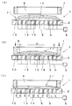
- FIG. 1A and 1B are schematic views showing a holding device according to Embodiment 1, wherein FIG. 3A is a plan view, and FIG. (A)-(c) is a schematic sectional drawing which shows the process in which the sealed board
- FIG. FIG. 3 is a schematic diagram illustrating a holding device according to a second embodiment, where (a) is a plan view and (b) is a cross-sectional view taken along line BB.
- (A)-(b) is a schematic sectional drawing which shows the process of measuring the thickness of the board
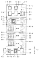
- FIG. 6 it is a top view which shows the outline
- A)-(d) is a schematic sectional drawing which shows the process of resin-sealing using the resin molding apparatus of Embodiment 6.
- the “object” includes a substrate and a composite in which an insulator or a conductor is formed on the substrate.
- the “substrate” includes a general substrate such as a glass epoxy laminate, a printed substrate, a glass substrate, a metal substrate, a semiconductor wafer, and the like.
- the “resin-sealed product” is a resin-sealed object and includes a sealed substrate described later.
- Embodiment 1 (Configuration of holding device) The structure of the holding device according to the present invention will be described with reference to FIG.
- the holding device is a holding device that holds an object in close contact with the table by vacuum suction.
- the object to be held is a substrate or a complex in which an insulator, metal, or the like is formed on the substrate.
- Embodiment 1 shows an example in which a substrate having a rectangular shape as an object is held in close contact with a table.
- the substrate for example, a glass epoxy laminated plate, a printed substrate, a ceramic substrate, a lead frame, or the like is used. Alternatively, a sealed substrate in which a sealing resin is molded on these substrates is used.
- the holding device 1 includes a table 2 on which a substrate is placed and a plurality of suction holes 3 provided in the table 2.
- a plurality of suction holes 3 are formed in the table 2 in a lattice shape. In FIG. 1, ten suction holes 3 are formed along the longitudinal direction, and five suction holes 3 are formed along the lateral direction. Therefore, a total of 50 suction holes 3 are formed in the table 2. As shown in FIG. 1B, each suction hole 3 penetrates from the front surface to the back surface of the table 2.
- the number of the suction holes 3 is arbitrarily set according to the size of the substrate 4 to be held (portion indicated by a two-dot chain line in the drawing) and the deformed state of the substrate 4 (for example, the state of distortion or warpage of the substrate). can do.
- the plurality of suction holes 3 are connected to the decompression mechanism 6 via pipes 5 connected to the respective suction holes 3.
- a vacuum pump or the like is used as the decompression mechanism 6.
- the holding device 1 is provided with a pressing member 7 for pressing the periphery of the substrate 4 against the table 2 in accordance with the shape and size of the substrate 4.
- the pressing member 7 is configured by, for example, a frame-shaped member having an opening 8 in the vertical direction.
- the pressing member 7 is a pressing member that presses only the periphery of the substrate 4 and does not press the central portion of the substrate 4.
- the pressing member 7 is raised and lowered by a drive mechanism (not shown) provided in the holding device 1.
- PEEK Poly Ether Ether Ketone
- a buffer member or an elastic member may be provided on the bottom surface of the pressing member 7.
- the table 2 is provided with sealing grooves 9 surrounding the plurality of suction holes 3.
- a sealing material 10 such as an O-ring is disposed in the sealing groove 9.
- the sealing material 10 is disposed so that the upper portion of the sealing material 10 protrudes from the surface of the table 2.
- the sealing material 10 it is preferable to use silicone rubber, fluorine rubber, or the like.
- the sealing material 10 is preferably made of a material having an appropriate hardness and easily stretched.
- a frame-shaped pressing member 7 is disposed above the position where the sealing material 10 is disposed.
- the sealing material 10 is enclosed in the frame-shaped pressing member 7 in plan view.
- FIG. 1A when the state in which the pressing member 7 and the sealing material 10 overlap is drawn as a plan view, the sealing material 10 is completely included in the pressing member 7. Therefore, as will be described later, as shown in FIG. 2B, the periphery of the substrate 4 (the sealed substrate 11 in FIG. 2) is sandwiched between the sealing material 10 and the pressing member 7 disposed on the table 2. In this state, it is pressed against the table 2. (Operation of holding device)
- FIGS. 1 and 2 With reference to FIGS. 1 and 2, the operation of holding the object in close contact with the table 2 in the holding device 1 will be described.
- FIG. 2 an example will be described in which, as an object, for example, a sealed substrate in which a sealing resin is molded on the substrate is held in close contact with the table 2.
- the sealed substrate 11 is placed at a predetermined position on the table 2.
- the sealed substrate 11 includes, for example, a substrate 12 made of a printed circuit board or a lead frame, a plurality of chip-like components (not shown) mounted in a plurality of regions of the substrate 12, and a plurality of regions collectively. And a sealing resin 13 molded so as to be covered. If the difference between the thermal expansion coefficient of the substrate 12 and the thermal expansion coefficient of the sealing resin 13 is large, the sealed substrate 11 is deformed when the sealed substrate 11 is taken out of the mold and brought to a room temperature lower than the molding temperature. There are things to do. In FIG. 2, as an example in which the sealed substrate 11 is deformed, for example, an example in which a warp that is convex on the surface side (the side on which the sealing resin 13 is molded) of the sealed substrate 11 occurs. Show.
- the sealed substrate 11 having a warp that is convex on the surface side is placed on the table 2, the sealed substrate 11 and the table 2 are brought into close contact with each other.
- a gap 14 is generated between the sealed substrate 11 and the table 2. If the gap 14 is large, the suction force is weak even if the sealed substrate 11 is sucked by the decompression mechanism 6, and the sealed substrate 11 may not be attracted to the table 2. Further, even if the sealed substrate 11 is sucked by the decompression mechanism 6, if the air leaks between the sealed substrate 11 and the table 2, the sealed substrate 11 may not be sufficiently adsorbed to the table 2. is there. This phenomenon becomes particularly remarkable in the sealed substrate 11 having a large area. The fact that the sealed substrate 11 cannot be attracted to the table 2 means that the warped of the sealed substrate 11 can be corrected to be flat and the sealed substrate 11 cannot be brought into close contact with the table 2.
- the pressing member 7 is lowered from a predetermined position by using a drive mechanism (not shown) provided in the holding device 1.
- the bottom surface of the pressing member 7 is brought into contact with the periphery of the sealed substrate 11, and the periphery of the sealed substrate 11 is brought into close contact with the sealing material 10 by the pressing member 7.
- the sealed substrate 11 is further pressed in a state where the periphery of the sealed substrate 11 is in close contact with the sealing material 10.
- a sealed space 15 can be formed between the sealed substrate 11 and the table 2 via the sealing material 10. Therefore, it is possible to prevent air from leaking to the outside from the sealed space 15 formed between the sealed substrate 11 and the table 2.
- the pressure-reducing mechanism 6 and the sealed substrate 11 are pressed with the pressing member 7 pressed against the table 2 through the sealing material 10 around the sealed substrate 11.
- Air present in the sealed space 15 formed between the table 2 is sucked.
- the pressure in the sealed space 15 changes from atmospheric pressure to negative pressure (vacuum). Since the pressure in the sealed space 15 is smaller than the atmospheric pressure, a force for pressing the sealed substrate 11 against the table 2 is generated by the atmospheric pressure.
- the sealed substrate 11 is attracted to the table 2 by the vacuum mechanism 6 sucking the sealed substrate 11. Thereby, the warp of the sealed substrate 11 can be corrected to be flat and the sealed substrate 11 can be brought into close contact with the table 2.
- sucking the sealed substrate 11 to the table 2 through the plurality of suction holes 3 the sealed substrate 11 can be held in close contact with the table 2.
- the area occupied by the sealed space 15 formed between the sealed substrate 11 and the table 2 corresponds to a vacuum adsorption area (pressure receiving area).
- the area of the spatial region in the region indicated by A in FIG. 2B in other words, the surface area on the substrate 12 side of the pre-sealing substrate 11 not in contact with the table 2 corresponds to the pressure receiving area.
- the larger the pressure receiving area the larger the force received from the atmospheric pressure, and the suction force for sucking the sealed substrate 11 to the table 2 increases. Therefore, even when the area of the sealed substrate 11 is large or the warp of the sealed substrate 11 is large, the warp of the sealed substrate 11 is corrected to be flat and the sealed substrate 11 is brought into close contact with the table 2.
- the holding device 1 includes a table 2 on which a sealed substrate 11 as an object is placed, a plurality of suction holes 3 provided on the table 2 for sucking the sealed substrate 11, and the table 2.
- a sealing member 10 that surrounds the periphery of the plurality of suction holes 3, a pressing member 7 that presses the periphery of the sealed substrate 11 against the table 2 at a position where the sealing member 10 is disposed, and a plurality of suction holes 3.
- the pressure reducing mechanism 6 to be connected is provided.
- a sealed space 15 is formed between the sealed substrate 11 and the table 2, and the air existing in the sealed space 15 is sucked to place the sealed substrate 11 on the table 2. Pull and stick. Therefore, the warped of the sealed substrate 11 can be corrected to be flat and the sealed substrate 11 can be held in close contact with the table 2.
- the table 2 is provided with a plurality of suction holes 3 for sucking the sealed substrate 11 as a target object and the sealing material 10 surrounding the suction holes 3.
- a pressing member 7 that presses the periphery of the sealed substrate 11 against the table 2 is provided at a position where the sealing material 10 is disposed. Even when warpage occurs in the sealed substrate 11, by pressing the periphery of the sealed substrate 11 with the pressing member 7, the sealed substrate 11, the table 2, A sealed space 15 can be formed between the two.
- the pressure reduction mechanism 6 is used to suck the air present in the sealed space 15.
- the pressure in the sealed space 15 becomes smaller than the atmospheric pressure, and a force for pressing the sealed substrate 11 against the table 2 is generated by the atmospheric pressure.
- the decompression mechanism 6 sucks the sealed substrate 11, the sealed substrate 11 is attracted to and brought into close contact with the table 2. Therefore, the warp of the sealed substrate 11 can be corrected to be flat, and the sealed substrate 11 can be held in close contact with the table 2.
- the sealed substrate 11 is brought into close contact with the table 2 by sucking the air present in the sealed space 15 formed between the sealed substrate 11 and the table 2. Since the area occupied by the sealed space 15 corresponds to the vacuum pressure receiving area, the suction force for sucking the sealed substrate 11 to the table 2 increases as the area occupied by the sealed space 15 increases. Therefore, even when the area of the sealed substrate 11 is large or the warp of the sealed substrate 11 is large, the warp of the sealed substrate 11 is corrected to be flat and the sealed substrate 11 is brought into close contact with the table 2. Can be held in a state of being allowed to enter.
- a force for pressing the sealed substrate 11 against the table 2 is generated by atmospheric pressure.
- the warp of the sealed substrate 11 is corrected to be flat, and the sealed substrate 11 is brought into close contact with the table 2.
- the sealed substrate 11 may slide on the sealing material 10 by loosening the pressing force of the pressing member 7 or making the sealing material 10 easy to slide. Thereby, it is possible to prevent the sealed substrate 11 from being damaged by correcting the warpage of the sealed substrate 11.
- the holding device 16 is a holding device that holds a substrate (object) having a circular shape in close contact with the table.
- a wafer or a wafer level package in which a sealing resin is molded on the wafer is used.
- the holding device 16 includes a table 17 on which a circular substrate is placed and a plurality of suction holes 3 provided in the table 17.
- a plurality of suction holes 3 are formed in a circumferential shape.
- the number of the suction holes 3 is arbitrarily set according to the size of the substrate 18 to be held (portion indicated by a two-dot chain line in the drawing), the deformed state of the substrate 18 (the state of distortion or warpage of the substrate), and the like. Can do.
- the plurality of suction holes 3 are connected to the decompression mechanism 6 via pipes 5 connected to the respective suction holes 3.
- As the decompression mechanism 6, a vacuum pump or the like is used.
- the holding device 16 is provided with a pressing member 19 for pressing the periphery of the substrate 18 against the table 17 in accordance with the size of the substrate 18.
- the pressing member 19 is configured by an annular member having an opening 20 in the vertical direction.
- polyether ether ketone: PEEK (PolyPoEther Ether Ketone) or the like is used as the pressing member 19.
- a buffer member or an elastic member may be provided on the bottom surface of the pressing member 19.
- the pressing member 19 is moved up and down by a drive mechanism (not shown) provided in the holding device 16.
- the table 17 is provided with a sealing groove 21 that surrounds the periphery of the plurality of suction holes 3.
- a sealing material 22 is disposed in the sealing groove 21. Therefore, the periphery of the substrate 18 is pressed against the table 17 while being sandwiched between the sealing material 22 and the pressing member 19 disposed on the table 17.
- a wafer such as a silicon wafer or a compound semiconductor wafer, or a wafer level package that is resin-sealed in a wafer state can be held on the table 17.
- the holding device 16 may be provided with an annular pressing member that presses the periphery of the wafer corresponding to the diameter of the wafer.
- a plurality of suction holes 3 are formed in the table 17 in a circumferential shape.
- the position of the plurality of suction holes 3 can be set arbitrarily.
- the suction holes 3 may be formed so as to correspond to the respective chip regions where the manufacturing process in the semiconductor pre-process is completed and the wafer is divided and separated into individual pieces.
- the holding device 16 Since the operation of the holding device 16 is the same as that of the holding device 1 shown in the first embodiment, the description thereof is omitted.
- the holding device 16 has the same effect as the holding device 1 shown in the first embodiment.
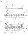
- Embodiment 3 (Configuration of inspection equipment) With reference to FIG. 4, the inspection apparatus used in Embodiment 3 will be described.
- the inspection device is obtained by adding an inspection mechanism to the holding device 1 shown in the first embodiment or the holding device 16 shown in the second embodiment.
- the holding device can be used as an inspection device.
- the inspection mechanism for example, a mechanism for measuring the thickness of the substrate and a mechanism for inspecting the surface state of the substrate are added. Since the configuration and operation other than the inspection mechanism are the same as those of the holding device 1 of the first embodiment or the holding device 16 of the second embodiment, description thereof is omitted.
- the inspection device 23 has a configuration in which, for example, an inspection mechanism such as a contact displacement sensor, an optical displacement sensor, and an image processing system is further added to the holding device 1.
- an inspection mechanism such as a contact displacement sensor, an optical displacement sensor, and an image processing system is further added to the holding device 1.
- a contact displacement sensor or an optical displacement sensor as the inspection mechanism, the thickness of the substrate held in close contact with the table 2 can be accurately measured.
- an image processing system equipped with a CMOS (Complementary Metal Oxide Semiconductor) image sensor or CCD (Charge Coupled Device) image sensor as the inspection mechanism, substrate surface inspection, defect inspection, pattern inspection, etc. can be performed it can. Since the substrate is held in close contact with the table 2, an accurate inspection can be performed in a state in which the influence of deformation such as warpage or distortion is removed.
- the thickness of the substrate held on the table 2 can also be measured by applying an image recognition system.
- image processing general image processing such as binarization of an image captured by a camera and
- the inspection device 23 includes a contact-type displacement sensor 24 above the table 2.
- the contact-type displacement sensor 24 can be moved in the X direction, the Y direction, and the Z direction by a moving mechanism (not shown) provided in the inspection device 23.
- the thickness of the substrate can be measured at an arbitrary position.
- the pressing member 7 is configured to press only the periphery of the substrate and not the central portion of the substrate. In other words, the entire region of the sealing resin on the sealed substrate, which is important for inspection, or the entire region of the region where the semiconductor chip of the substrate before sealing is mounted can be inspected. Therefore, the contact-type displacement sensor 24 moves in the X direction, the Y direction, and the Z direction in the opening 8 of the pressing member 7. This makes it possible to measure the thickness of the substrate at an arbitrary position on the substrate.
- the pre-sealing substrate prevents the semiconductor chip and the like from being damaged by the pressing member.
- the contact-type displacement sensor 24 is lowered and the predetermined position P ⁇ b> 1 of the table 2 without the sealed substrate 11 being placed on the table 2.
- the predetermined position P1 of the table 2 corresponds to a position P2 (see FIG. 4B) where the thickness of the substrate 12 included in the sealed substrate 11 is measured.
- the height displacement h1 of the table surface is measured by the contact type displacement sensor 24.
- the measured height position h1 of the table surface is stored in a memory or the like as the reference height of the table 2.
- the contact-type displacement sensor 24 is raised to stand by above the predetermined position P1.
- the sealed substrate 11 having warpage is placed at a predetermined position of the table 2.
- the pressing member 7 is lowered to press the periphery of the sealed substrate 11 against the table 2.
- a sealed space 15 is formed between the sealed substrate 11 and the table 2 via the sealing material.
- the warp of the sealed substrate 11 is corrected to be flat, and the sealed substrate 11 is held in close contact with the table 2. In this state, the warped substrate 11 is corrected to be warped and adheres flatly on the table 2.
- the contact-type displacement sensor 24 is lowered and brought into contact with a predetermined position P2 of the substrate 12 included in the sealed substrate 11.
- the height position h2 of the substrate 12 is measured by the contact displacement sensor 24. Since the sealed substrate 11 is held in flat contact with the table 2, the height position h2 of the substrate 12 can be accurately measured.
- a difference (h2 ⁇ h1) between the measured height position h2 of the substrate 12 and the height position h1 of the table surface stored in advance is obtained. This difference (h2 ⁇ h1) corresponds to the thickness of the substrate 12 included in the sealed substrate 11 at the predetermined position P2 of the sealed substrate 11.
- the predetermined position P2 of the substrate 12 and the predetermined position P1 of the table 2 are the same measurement position in plan view. Therefore, the thickness of the substrate 2 at the predetermined position P2 can be accurately obtained by obtaining the difference (h2-h1) between the two height positions measured by the contact type displacement sensor 24. In this manner, the thickness of the substrate 12 included in the sealed substrate 11 can be accurately measured using the inspection apparatus 23 in a state where the sealed substrate 11 is adhered flatly on the table 2. it can. (Function and effect)
- the inspection apparatus 23 includes a table 2 on which the sealed substrate 11 as an object is placed, a plurality of suction holes 3 provided on the table 2 for sucking the sealed substrate 11, and the table 2.
- a contact displacement sensor 24 which is an inspection mechanism for inspecting the finished substrate 11 is provided.
- a sealed space 15 is formed between the sealed substrate 11 having warpage and the table 2 through the sealing material 10.
- the sealed substrate 11 is attracted to and brought into close contact with the table 2.
- the warp of the sealed substrate 11 can be corrected to be flat and the sealed substrate 11 can be held in close contact with the table 2. Therefore, the thickness of the substrate 12 included in the sealed substrate 11 can be accurately measured using the contact-type displacement sensor 24 in a state in which the influence of deformation such as warpage or distortion is removed.
- the inspection device 23 measures the thickness of the sealed substrate 11 and the pressing member 7 that presses the periphery of the sealed substrate 11 against the table 2 corresponding to the sealed substrate 11.
- a contact-type displacement sensor 24 is provided. Even when the sealed substrate 11 is deformed such as warping or distortion, the sealed substrate 11 is pressed via the sealing material 10 by pressing the periphery of the sealed substrate 11 with the pressing member 7. A sealed space 15 can be formed between 11 and the table 2.
- the pressure reduction mechanism 6 is used to suck the air present in the sealed space 15.
- the deformation of the sealed substrate 11 can be corrected and the sealed substrate 11 can be brought into close contact with the table 2.
- the thickness of the substrate 12 included in the sealed substrate 11 is measured using the contact displacement sensor 24. Therefore, the thickness of the substrate 12 included in the sealed substrate 11 can be accurately measured in a state in which the influence of deformation such as warpage or distortion is removed.
- the sealed substrate 11 is placed on the table 2, the warpage of the sealed substrate 11 is corrected to be flat, and the sealed substrate 11 is brought into close contact with the table 2.
- the contact-type displacement sensor 24 is used to measure the height position h2 of the substrate 12 at the predetermined position P2 of the sealed substrate 11.
- the thickness of the substrate 12 included in the sealed substrate 11 can be accurately obtained. . Therefore, the thickness of the substrate 12 included in the sealed substrate 11 can be accurately measured in a state in which the influence of deformation such as warpage or distortion is removed.
- the sealed substrate 11 is brought into close contact with the table 2 by sucking the air present in the sealed space 15 formed between the sealed substrate 11 and the table 2. Since the area occupied by the sealed space 15 corresponds to a vacuum pressure receiving area, even when the area of the sealed substrate 11 is large or the warp of the sealed substrate 11 is large, the warp of the sealed substrate 11 is flat. And the sealed substrate 11 can be brought into close contact with the table 2. Therefore, even in the sealed substrate 11 having a large area or the sealed substrate 11 having a large warp, the substrate 12 of the sealed substrate 11 has the sealed substrate 11 in close contact with the table 2. Thickness can be measured accurately.
- the case where only one thickness of the substrate 12 included in the sealed substrate 11 is measured is shown for convenience. Not only this but the thickness of the board
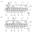
- the sealed substrate 11 having warpage is placed on a predetermined position of the table 2.
- the periphery of the sealed substrate 11 is pressed against the table 2 by lowering the pressing member 7.
- the warpage of the sealed substrate 11 is corrected to be flat and the sealed substrate 11 is brought into close contact with the table 2. In this state, the sealed substrate 11 is held flat on the table 2.
- the contact-type displacement sensor 24 is lowered and brought into contact with the predetermined position P2 of the sealed substrate 11.
- the height position h2 of the substrate 12 included in the sealed substrate 11 is measured by the contact-type displacement sensor 24.
- the measured height position h2 of the substrate 12 is stored in a memory or the like as the relative height of the substrate 12 included in the sealed substrate 11.
- the contact-type displacement sensor 24 is raised, and the contact-type displacement sensor 24 is moved to a predetermined position above the sealing resin 13 of the sealed substrate 11.
- the contact-type displacement sensor 24 is lowered and brought into contact with the predetermined position P3 of the sealed substrate 11.
- the height position h3 of the sealed substrate 11 is measured by the contact displacement sensor 24.
- the difference (h3 ⁇ h2) between the measured height position h3 of the sealed substrate 11 and the relative height position h2 of the substrate 12 stored in advance is obtained.
- This difference (h3 ⁇ h2) corresponds to the relative thickness of the sealing resin 13 included in the sealed substrate 11.
- the sealed substrate 11 is held in close contact with the table 2 in a state where the warpage is corrected to be flat. Therefore, the height position h2 of the substrate 12 included in the sealed substrate 11 and the height position h3 of the sealed substrate 11 using the contact-type displacement sensor 24 in a state where the influence of deformation such as warpage and distortion is removed. Both of them can be measured. Therefore, by obtaining the difference (h3 ⁇ h2) in the measured height position, it is possible to easily obtain the thickness of the sealing resin 13 that has conventionally been difficult to measure.
- the sealed substrate 11 is adsorbed to the table 2 by sucking the air present in the sealed space 15 formed between the sealed substrate 11 and the table 2. Since the area occupied by the sealed space 15 corresponds to a vacuum pressure receiving area, even when the area of the sealed substrate 11 is large or the warp of the sealed substrate 11 is large, the warp of the sealed substrate 11 is flat. And the sealed substrate 11 can be held in close contact with the table 2. Therefore, even in the sealed substrate 11 having a large area or the sealed substrate 11 having a large warp, the sealing resin included in the sealed substrate 11 with the sealed substrate 11 in close contact with the table 2. The thickness of 13 can be determined relatively.
- the thickness of the sealing resin 13 of the sealed substrate 11 that is resin-sealed in the resin molding apparatus can be relatively determined. Therefore, it is possible to easily manage the film thickness of the sealing resin 13, which has been difficult in the past, in other words, to manage the thickness of the package that will eventually become a product. As a result, the molding process in the resin molding apparatus can be managed stably and easily.
- the case where only one thickness of the sealing resin 13 included in the sealed substrate 11 is measured is shown for convenience.
- the thickness of the substrate 12 and the sealed substrate 11 at a plurality of positions can be similarly measured using the contact displacement sensor 24. In that case, the average value and variation of the relative thickness of the sealing resin 13 included in the sealed substrate 11 can be obtained.
- Emodiment 5 With reference to FIG. 6, the operation
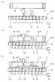
- the contact-type displacement sensor 24 is moved above the measurement position in a state where nothing is placed on the table 2 in the inspection device 23.
- the contact-type displacement sensor 24 is lowered and brought into contact with a predetermined position P4 of the table 2.
- the predetermined position P4 of the table 2 includes a position P5 (see FIG. 6B) for measuring the thickness of the substrate 12 included in the pre-sealing substrate 26 and a position P6 (see FIG. 6) for measuring the thickness of the sealed substrate 11. (C)).
- the height displacement h4 of the table surface is measured by the contact type displacement sensor 24.
- the measured height h4 of the table surface is stored in a memory or the like as a reference height.
- the contact-type displacement sensor 24 is raised to stand by above the predetermined position P4.
- the pre-sealing substrate 26 on which the plurality of semiconductor chips 25 are mounted is placed at a predetermined position on the table 2.
- the periphery of the substrate 26 before sealing is pressed against the table 2 by lowering the pressing member 7.
- the deformation of the pre-sealing substrate 26 is corrected and the pre-sealing substrate 26 is brought into close contact with the table 2. In this state, the deformation of the pre-sealing substrate 26 is corrected and held flat on the table 2.
- the contact type displacement sensor 24 is lowered and brought into contact with a predetermined position P5 of the substrate 26 before sealing.
- the predetermined position P5 of the substrate 26 before sealing is a region where the semiconductor chip 25 is not mounted and the upper surface of the substrate 12 is exposed.
- the height position h5 of the substrate 26 before sealing is measured by the contact displacement sensor 24.
- a difference (h5 ⁇ h4) between the measured height position h5 of the substrate 26 before sealing and the reference height position h4 of the table surface stored in advance is obtained.
- This difference (h5 ⁇ h4) corresponds to the thickness of the substrate 12 included in the pre-sealing substrate 26 at the predetermined position P5 of the pre-sealing substrate 26.
- the height position h5 of the substrate 26 before sealing is stored in a memory or the like.
- the contact-type displacement sensor 24 is raised and waited above the predetermined position P5.
- the pressing member 7 is raised and stopped at the original position.
- the substrate 26 before sealing is taken out from the table 2.
- the inspection apparatus 23 returns to the initial standby state.
- the sealed substrate 11 is placed at a predetermined position on the table 2.
- This sealed substrate 11 is a sealed substrate obtained by resin-sealing the unsealed substrate 26 whose height position h5 is measured at the predetermined position P5 described above. Therefore, the pre-sealing substrate 26 and the sealed substrate 11 are placed at the same position on the table 2 of the inspection apparatus 23.
- the periphery of the sealed substrate 11 is pressed against the table 2 by lowering the pressing member 7.
- sucking the sealed substrate 11 using the decompression mechanism 6 the deformation of the sealed substrate 11 is corrected and the sealed substrate 11 is brought into close contact with the table 2. In this state, the sealed substrate 11 is held flat on the table 2.
- the contact-type displacement sensor 24 is lowered and brought into contact with the predetermined position P6 of the sealed substrate 11.
- the height position h6 of the sealed substrate 11 is measured by the contact displacement sensor 24.
- a difference (h6 ⁇ h5) between the measured height position h6 of the sealed substrate 11 and the height position h5 of the pre-sealing substrate 26 stored in advance is obtained.
- This difference (h6 ⁇ h5) corresponds to the thickness of the sealing resin 13 of the sealed substrate 11 at the predetermined position P6 of the sealed substrate 11.
- the sealed substrate 11 has the same position as the sealed substrate 11 in a state where the deformation of the pre-sealed substrate 26 and the sealed substrate 11 is corrected and held flat on the table 2.
- the thickness of the substrate 12 and the thickness of the sealing resin 13 can be accurately measured.
- the pre-sealing substrate 26 and the sealed substrate 11 are held in close contact with the table 2 in a state where the deformation is corrected. Therefore, in a state in which the influence of deformation such as warpage and distortion is removed, the contact-type displacement sensor 24 is used, and the height position h5 of the substrate 12 of the sealed substrate 11 at the same position and the sealed substrate 11 The height position h6 can be accurately measured. Therefore, from these height positions h6 and h5 and the reference height position h4 of the table surface at the same position, the thickness of the substrate 12 included in the sealed substrate 11 and the thickness of the sealing resin 13 are accurately measured. Can do.
- the deformation of the pre-sealing substrate 26 and the sealed substrate 11 is corrected and held in close contact with the table 2. be able to. Therefore, even in the sealed substrate 11 having a large area or the sealed substrate 11 having a large warp, the thickness of the substrate 12 and the thickness of the sealing resin 13 included in the sealed substrate 11 are accurately measured. be able to.
- the contact-type displacement sensor 24 can be used to measure the thickness of the substrate 12 and the thickness of the sealing resin 13 included in the sealed substrate 11 at a plurality of positions. In that case, the average value and variation of the thickness of the substrate 12 and the thickness of the sealing resin 13 included in the sealed substrate 11 can be obtained.
- the reference height position h4 of the table surface at the same position, the height position h5 of the substrate 12 included in the sealed substrate 11, and the sealed substrate 11
- the height position h6 was measured, and the thickness of the substrate 12 included in the sealed substrate 11 and the thickness of the sealing resin 13 were obtained.
- the measurement of the reference height position h4 on the table surface can be performed at the start of production, and the value can be shared.
- the reference height position h4 of the table surface is measured, and the value is shared according to the number of times of resin sealing. In this way, the number of measurements of the reference height position h4 can be reduced.
- the thickness of the substrate 12 and the thickness of the sealing resin 13 were determined for the sealed substrate 11 having a two-layer structure including the substrate 12 and the sealing resin 13. Not only this but the board
- the height position of the pre-sealing substrate 26 is measured by the contact displacement sensor 24 in a state where the pre-sealing substrate 26 is in close contact with the table 2.
- the state of the chip of the semiconductor chip 25 can be inspected in the state where the substrate 26 before sealing is in close contact with the table 2. In this case, it is determined whether the semiconductor chip 25 is normally disposed on the substrate 12 using the contact displacement sensor, the optical displacement sensor, the image recognition system, the line sensor, or the like, and there is no chipping. Can be inspected. When the semiconductor chip 25 is missing, the amount of resin supplied when resin molding can be adjusted.
- Embodiment 6 (Configuration of resin molding equipment) With reference to FIG. 7, the resin molding apparatus of Embodiment 6 is demonstrated.
- the resin molding apparatus shown in FIG. 7 is a resin molding apparatus provided with the inspection apparatus 23 described so far. In FIG. 7, for example, a resin molding apparatus using a compression molding method is shown.
- the resin molding apparatus 27 includes a substrate supply / storage module 28, an inspection module 29, three molding modules 30A, 30B, and 30C, and a resin supply module 31 as components.
- the substrate supply / storage module 28, the inspection module 29, the molding modules 30A, 30B, and 30C, and the resin supply module 31, which are constituent elements, can be attached to and detached from other constituent elements, respectively. And can be exchanged.
- the substrate supply / storage module 28 includes a pre-sealing substrate supply unit 32 for supplying the pre-sealing substrate 26, a sealed substrate storage unit 33 for storing the sealed substrate 11, the pre-sealing substrate 26 and the sealing.
- a substrate platform 34 for delivering the stopped substrate 11 and a substrate transport mechanism 35 for transporting the pre-sealing substrate 26 and the sealed substrate 11 are provided.
- the substrate platform 34 moves in the Y direction within the substrate supply / storage module 28.
- the substrate transport mechanism 35 moves in the X direction, the Y direction, and the Z direction in the substrate supply / storage module 28, the inspection module 29, and the molding modules 30A, 30B, and 30C.
- the predetermined position S1 is a position to stand by when the substrate transport mechanism 35 does not operate.
- the inspection module 29 is provided with the inspection device 23 shown in the third to fifth embodiments.
- the inspection device 23 includes a table 2, a decompression mechanism 6, a pressing member 7, and a contact displacement sensor 24. Using the inspection apparatus 23, the height position serving as the reference of the table 2, the height position of the substrate 12 included in the pre-sealing substrate 26, the height position of the substrate 12 included in the sealed substrate 11, and the sealed substrate 11 is inspected as necessary, such as the height position of 11 and the arrangement state of the semiconductor chips on the substrate 26 before sealing.
- Each molding module 30A, 30B, 30C is provided with a lower mold 36 that can be moved up and down, and an upper mold (see FIG. 8) that is disposed to face the lower mold 36.
- the lower mold 36 is provided with a cavity 37 to which a resin material is supplied.
- a release film supply mechanism 38 (a rectangular portion indicated by a two-dot chain line in FIG. 7) for supplying a long release film to the lower mold 36 is provided.
- Each of the molding modules 30A, 30B, and 30C includes a mold clamping mechanism 39 (circular portion indicated by a two-dot chain line in FIG. 7) that molds and clamps the upper mold and the lower mold 36.
- the resin supply module 31 includes an XY table 40, a resin container 41 placed on the XY table 40, a resin material loading mechanism 42 for loading a resin material into the resin container 41, a resin A resin transport mechanism 43 that transports the accommodating portion 41 is provided.
- the XY table 40 moves in the X direction and the Y direction in the resin supply module 31.
- the resin transport mechanism 43 moves in the X direction, the Y direction, and the Z direction within the resin supply module 31 and the respective molding modules 30A, 30B, and 30C.
- the predetermined position R1 is a position to stand by when the resin transport mechanism 43 does not operate.
- the substrate supply / storage module 28 is provided with a control unit CTL.
- the control unit CTL performs transport of the pre-sealing substrate 26 and the sealed substrate 11, transport of the resin material, mold clamping and mold opening, thickness measurement of the pre-sealing substrate 26 and the sealed substrate 11, and the like. Control.
- the control unit CTL may be provided in the inspection module 29, each molding module 30A, 30B, 30C, or the resin supply module 31. (Operation of resin molding equipment) With reference to FIGS. 7 to 8, the operation of resin sealing using the resin molding device 27 will be described.
- the unsealed substrate 26 is sent from the unsealed substrate supply unit 32 to the substrate mounting unit 34.
- the substrate transport mechanism 35 is moved in the ⁇ Y direction from the predetermined position S1, and the substrate transport mechanism 35 receives the pre-sealing substrate 26 from the substrate platform 34.
- the substrate transport mechanism 35 is returned to the predetermined position S1.
- the substrate transport mechanism 35 is moved in the + X direction to the predetermined position M1 of the molding module 30B.
- the substrate transport mechanism 35 is moved in the ⁇ Y direction to stop at a predetermined position C1 above the lower die 36.
- a release film 44 (see FIG. 8A) is supplied from the release film supply mechanism 38 to the lower mold 36.
- the substrate transport mechanism 35 is raised to supply the pre-sealing substrate 26 to the upper mold 45 (see FIG. 8A).
- the substrate transport mechanism 35 is returned to the predetermined position S1 of the substrate supply / storage module 28.
- the XY table 40 is moved in the ⁇ Y direction, and the n resin accommodating portion 41 is stopped at a predetermined position below the resin material charging mechanism 42.
- a predetermined amount of resin material is supplied from the resin material charging mechanism 42 to the resin accommodating portion 41.
- the XY table 40 is returned to its original position.
- the resin transport mechanism 43 is moved in the ⁇ Y direction from the predetermined position R1.
- the resin transport mechanism 43 receives the resin container 41 placed on the XY table 40.
- the resin transport mechanism 43 is returned to the predetermined position R1.
- the resin transport mechanism 43 is moved in the ⁇ X direction to the predetermined position M1 of the molding module 30B.
- the resin transport mechanism 43 is moved in the ⁇ Y direction and stopped at a predetermined position C1 above the lower die 36.
- the resin transport mechanism 43 is lowered and the resin material 46 (see FIG. 8A) is supplied from the resin container 41 to the cavity 37.
- the resin transport mechanism 43 is returned to the predetermined position R1.
- FIG. 8A shows a case where a granular resin is supplied as the resin material 46.
- the resin material 46 is melted to produce a fluid resin 47.
- the lower mold 36 is raised by the mold clamping mechanism 39 (see FIG. 7), and the upper mold 45 and the lower mold 36 are clamped.
- the semiconductor chip 25 mounted on the pre-sealing substrate 26 is immersed in the fluid resin 47 melted in the cavity 37.
- the fluid resin 47 is heated only for the time necessary to cure the fluid resin 47.
- the fluid resin 47 is cured to form the cured resin 48.
- the semiconductor chip 25 mounted on the pre-sealing substrate 26 is resin-sealed with the cured resin 48 molded corresponding to the shape of the cavity 37.
- the substrate transport mechanism 35 is moved from the predetermined position S1 of the substrate supply / storage module 28 to the predetermined position M1 of the molding module 30B. Further, the substrate transport mechanism 35 is moved to a predetermined position C1 above the lower mold 36, and the sealed substrate 11 is received by the substrate transport mechanism 35.
- the substrate transport mechanism 35 is moved from the molding module 30B to the inspection module 29, and stopped at a predetermined position E1 above the table 2 of the inspection apparatus 23.
- the sealed substrate 11 is delivered from the substrate transport mechanism 35 to the inspection apparatus 23.
- the substrate transport mechanism 35 is returned to the predetermined position S1.
- the control unit CTL compares these height positions to determine the relative thickness of the sealing resin 13 included in the sealed substrate 11.
- the substrate transport mechanism 35 is moved to a predetermined position E1 above the table 2 of the inspection apparatus 23, and the sealed substrate 11 is received from the inspection apparatus 23.
- the substrate transport mechanism 35 is moved to deliver the sealed substrate 11 to the substrate platform 34.
- the sealed substrate 11 is stored in the sealed substrate storage unit 33 from the substrate platform 34.
- the resin sealing is completed by the steps so far.
- the inspection device 23 is provided in the inspection module 29 of the resin molding device 27.
- the inspection device 23 uses the inspection device 23, the height position of the substrate 12 included in the pre-sealing substrate 26 and the sealing in a state where the deformation of the pre-sealing substrate 26 or the sealed substrate 11 is corrected and brought into close contact with the table 2
- the height position of the substrate 12 included in the finished substrate 11 and the height position of the sealed substrate 11 can be measured.
- the thickness of the sealing resin 13 included in the sealed substrate 11 can be accurately obtained. Therefore, the resin molding process in the resin molding device 27 can be steadily managed. This makes it possible to operate the resin molding device 27 stably.
- the inspection device 23 is provided in the resin molding device 27 using the compression molding method.
- the inspection apparatus 23 of the present invention can be provided not only in this but also in a resin molding apparatus using a transfer molding method or an injection molding method.
- the inspection device 23 is integrated with the inspection module 29 of the resin molding device 27. Not limited to this, the inspection device 23 may be installed separately from the resin molding device 27. In this case, the thickness of the sealing resin molded in the plurality of resin molding apparatuses can be measured by one inspection apparatus 23.
- the height position of the table 2 the height position of the substrate 12 included in the pre-sealing substrate 26, and the substrate included in the sealed substrate 11 are used.
- the case where the contact type displacement sensor 24 is provided in the inspection device 23 as the inspection mechanism is shown.
- both the contact-type displacement sensor 24 and the image processing system can be provided in the inspection apparatus 23.
- the thickness measurement of the substrate 12 included in the sealed substrate 11, the thickness measurement of the sealing resin 13 included in the sealed substrate 11, and the surface inspection and defect inspection of the sealed substrate 11 are performed. This can be done using the inspection device 23. Further, the chip state of the semiconductor chip can be inspected on the pre-sealing substrate 26.
- the holding device surrounds the table on which the object is placed, the plurality of suction holes provided on the table for sucking the object, and the periphery of the plurality of suction holes provided on the table.
- the seal member is configured to include a pressing member that presses the periphery of the object against the table at a position where the seal member is disposed, and a decompression mechanism connected to the plurality of suction holes.
- the deformation of the object can be corrected and the object can be held in close contact with the table.
- the inspection apparatus includes a table on which an object is placed, a plurality of suction holes provided on the table for sucking the object, a sealing material provided on the table and surrounding the plurality of suction holes, and a seal At the position where the material is disposed, a pressing member that presses the periphery of the object against the table, a decompression mechanism connected to the plurality of suction holes, and the periphery of the object is pressed by the pressing member, and a plurality of suction is performed by the decompression mechanism An inspection mechanism that inspects the object in a state in which the object is sucked through the hole.
- the inspection mechanism includes any one of a contact displacement sensor, an optical displacement sensor, and an image processing system.
- the resin molding apparatus is configured to include the inspection apparatus of the above embodiment.
- the inspection method includes a step of placing an object on a table provided with a plurality of suction holes and a sealing material surrounding the plurality of suction holes, and a pressing member at a position where the sealing material is disposed. Pressing the periphery of the object against the table, forming the space between the table and the object by pressing the periphery of the object, and sucking the air in the space through the plurality of suction holes. This includes a step of bringing the object into close contact with the table and a step of inspecting the object using the inspection mechanism while the object is in close contact with the table.
- the object is a pre-sealing substrate or a sealed substrate, and the object is inspected by using an inspection mechanism.
- the inspection step includes the step of measuring the reference height information of the table using the inspection mechanism in a state where the object is not placed on the table, and the table of the object. Measuring the height information of the object using an inspection mechanism in close contact with the object, and comparing the height information of the object with the reference height information of the table. Ask for.
- the reference thickness information of the table and the height information of the object measured with the object in close contact with the table are compared at the same position, whereby the thickness of the object is obtained more accurately. be able to.
- the object has a substrate and an insulator formed on the substrate, and the inspection step uses an inspection mechanism in a state where the object is in close contact with the table. And measuring the substrate height information and the insulator height information, and comparing the insulator height information with the substrate height information to determine the thickness of the insulator.
- the relative thickness of the insulator is obtained by comparing the height information of the substrate with the height information of the insulator in a state where the object having the substrate and the insulator is in close contact with the table. Can be easily obtained.
- the inspection mechanism is any one of a contact displacement sensor, an optical displacement sensor, and an image recognition system, and the thickness of the object is measured by using the inspection mechanism.
- the thickness of an object can be accurately obtained by using any one of a contact displacement sensor, an optical displacement sensor, and an image recognition system while the object is in close contact with the table. .
- the resin sealing method performs the inspection by the inspection method of the above embodiment after the resin sealing.
- the thickness of the substrate or the thickness of the sealing resin can be accurately obtained after the resin sealing.
- the resin sealing method performs inspection by the inspection method of the above embodiment before resin sealing, and performs inspection by the inspection method of the above embodiment even after resin sealing.
- the thickness of the substrate can be accurately determined before resin sealing, and the thickness of the sealing resin can be accurately determined after resin sealing.
- the resin-sealed product is manufactured by using the resin-sealed method of the above embodiment.
- a resin-sealed product can be manufactured by performing an inspection before and after resin sealing.
Landscapes
- Container, Conveyance, Adherence, Positioning, Of Wafer (AREA)
- Encapsulation Of And Coatings For Semiconductor Or Solid State Devices (AREA)
- Supply And Installment Of Electrical Components (AREA)
Abstract
変形した対象物であっても対象物の変形を矯正し安定してテーブルに保持するために、保持装置は、対象物が載置されるテーブルと、テーブルに設けられ対象物を吸引する複数の吸引孔と、テーブルに設けられ複数の吸引孔の周囲を取り囲むシール材と、シール材が配置された位置において、対象物の周囲をテーブルに押圧する押圧部材と、複数の吸引孔に接続される減圧機構とを備える。
Description
本発明は、保持装置、検査装置、検査方法、樹脂封止装置、樹脂封止方法及び樹脂封止品の製造方法に関する。
近年、樹脂封止された封止済基板(樹脂封止された封止済ウェーハを含む)などに要求される精度(寸法精度等)が高まってきている。そのため、樹脂封止前又は樹脂封止後に(あるいは、その両方で)、基板(ウェーハを含む)などを保持し、測定等をすることが増えてきている。
特許文献1には、複数の吸着穴で基板を吸着する保持装置が記載されている。
しかしながら、例えば、樹脂封止前に、基板に電子部品等が搭載される場合、その搭載により基板が湾曲する(歪む、反る)ことがある。
また、樹脂封止後においては、成形型からの取り出し後に樹脂封止後の基板が冷却されて収縮する際に、基板と封止樹脂との間の熱膨張係数(線膨張係数)の違いにより、基板が湾曲することがある。
従来の特許文献1に記載の保持装置では、基板が湾曲した場合、安定して基板を保持することができないことがあった。以下、本出願書類において、「基板が湾曲する」、「基板が歪む」、「基板が反る」ということを含めて「基板が変形する」と表現することがある。
上記の課題を解決するために、本発明に係る保持装置は、
対象物が載置されるテーブルと、
前記テーブルに設けられ前記対象物を吸引する複数の吸引孔と、
前記テーブルに設けられ前記複数の吸引孔の周囲を取り囲むシール材と、
前記シール材が配置された位置において、前記対象物の周囲を前記テーブルに押圧する押圧部材と、
前記複数の吸引孔に接続される減圧機構と、
を備える。
対象物が載置されるテーブルと、
前記テーブルに設けられ前記対象物を吸引する複数の吸引孔と、
前記テーブルに設けられ前記複数の吸引孔の周囲を取り囲むシール材と、
前記シール材が配置された位置において、前記対象物の周囲を前記テーブルに押圧する押圧部材と、
前記複数の吸引孔に接続される減圧機構と、
を備える。
上記の課題を解決するために、本発明に係る検査装置は、
対象物が載置されるテーブルと、
前記テーブルに設けられ対象物を吸引する複数の吸引孔と、
前記テーブルに設けられ前記複数の吸引孔の周囲を取り囲むシール材と、
前記シール材が配置された位置において、前記対象物の周囲を前記テーブルに押圧する押圧部材と、
前記複数の吸引孔に接続される減圧機構と、
前記押圧部材により前記対象物の周囲が押圧され、前記減圧機構により前記複数の吸引孔を介して前記対象物が吸引された状態において、前記対象物を検査する検査機構と、
を備える。
対象物が載置されるテーブルと、
前記テーブルに設けられ対象物を吸引する複数の吸引孔と、
前記テーブルに設けられ前記複数の吸引孔の周囲を取り囲むシール材と、
前記シール材が配置された位置において、前記対象物の周囲を前記テーブルに押圧する押圧部材と、
前記複数の吸引孔に接続される減圧機構と、
前記押圧部材により前記対象物の周囲が押圧され、前記減圧機構により前記複数の吸引孔を介して前記対象物が吸引された状態において、前記対象物を検査する検査機構と、
を備える。
上記の課題を解決するために、本発明に係る検査方法は、
複数の吸引孔と前記複数の吸引孔の周囲を取り囲むシール材とが設けられたテーブルに対象物を載置する工程と、
前記シール材が配置された位置において、押圧部材によって前記対象物の周囲を前記テーブルに押圧する工程と、
前記対象物の周囲を押圧することによって前記テーブルと前記対象物との間に空間を形成する工程と、
前記空間の空気を前記複数の吸引孔を介して吸引することによって前記対象物を前記テーブルに引き寄せて密着させる工程と、
前記対象物を前記テーブルに密着させた状態で検査機構を使用して前記対象物を検査する工程と、
を含む。
複数の吸引孔と前記複数の吸引孔の周囲を取り囲むシール材とが設けられたテーブルに対象物を載置する工程と、
前記シール材が配置された位置において、押圧部材によって前記対象物の周囲を前記テーブルに押圧する工程と、
前記対象物の周囲を押圧することによって前記テーブルと前記対象物との間に空間を形成する工程と、
前記空間の空気を前記複数の吸引孔を介して吸引することによって前記対象物を前記テーブルに引き寄せて密着させる工程と、
前記対象物を前記テーブルに密着させた状態で検査機構を使用して前記対象物を検査する工程と、
を含む。
本発明によれば、変形した(湾曲した、歪んだ、反った)対象物であっても、対象物の変形を矯正し安定してテーブルに保持することができる。
以下、本発明に係る実施形態について、図面を参照して説明する。本出願書類におけるいずれの図についても、わかりやすくするために、適宜省略し又は誇張して模式的に描かれている。同一の構成要素については、同一の符号を付して説明を適宜省略する。なお、本出願書類において、「対象物」とは、基板及び基板の上に絶縁体や導電体などが形成された複合体を含むものである。「基板」には、ガラスエポキシ積層板、プリント基板、ガラス基板、金属基板などの一般的な基板や半導体ウェーハなどが含まれる。「樹脂封止品」とは、樹脂封止された対象物であって、後述の封止済基板を含むものである。
〔実施形態1〕
(保持装置の構成)
本発明に係る保持装置の構成について、図1を参照して説明する。保持装置は、真空吸着によってテーブルの上に対象物を密着させて保持する保持装置である。保持する対象物は、基板又は基板の上に絶縁体や金属などが形成された複合体である。実施形態1においては、対象物として矩形状の形状を有する基板をテーブルの上に密着させて保持する例を示す。基板としては、例えば、ガラスエポキシ積層板、プリント基板、セラミックス基板、リードフレームなどが使用される。又は、これらの基板の上に封止樹脂が成形された封止済基板などが使用される。
〔実施形態1〕
(保持装置の構成)
本発明に係る保持装置の構成について、図1を参照して説明する。保持装置は、真空吸着によってテーブルの上に対象物を密着させて保持する保持装置である。保持する対象物は、基板又は基板の上に絶縁体や金属などが形成された複合体である。実施形態1においては、対象物として矩形状の形状を有する基板をテーブルの上に密着させて保持する例を示す。基板としては、例えば、ガラスエポキシ積層板、プリント基板、セラミックス基板、リードフレームなどが使用される。又は、これらの基板の上に封止樹脂が成形された封止済基板などが使用される。
図1(a)に示されるように、保持装置1は、基板が載置されるテーブル2とテーブル2に設けられた複数の吸引孔3とを備える。テーブル2には、複数の吸引孔3が格子状に形成される。図1においては、長手方向に沿って10個の吸引孔3が形成され、短手方向に沿って5個の吸引孔3が形成される。したがって、テーブル2には合計して50個の吸引孔3が形成される。図1(b)に示されるように、それぞれの吸引孔3はテーブル2の表面から裏面まで貫通する。吸引孔3の数は、保持する基板4(図において二点鎖線で示す部分)の大きさ及び基板4の変形した状態(例えば、基板の歪みや反りの状態)などに対応して任意に設定することができる。複数の吸引孔3は、それぞれの吸引孔3につながる配管5を介して減圧機構6に接続される。減圧機構6としては、例えば、真空ポンプなどが使用される。
保持装置1には、基板4の形状及び大きさに対応して基板4の周囲をテーブル2に押圧するための押圧部材7が設けられる。押圧部材7は、例えば、上下方向に開口部8を有する枠状部材によって構成される。押圧部材7は、基板4の周囲のみを押圧し、基板4の中央部などを押圧しない押圧部材である。押圧部材7は、保持装置1に設けられた駆動機構(図示なし)によって昇降する。押圧部材7としては、基板4に与える機械的なダメージを抑制する材料を用いることが好ましい。例えば、ポリエーテルエーテルケトン:PEEK(Poly Ether Ether Ketone )などが用いられる。押圧部材7の底面に緩衝部材又は弾性部材などを設けても良い。
図1(b)に示されるように、テーブル2には、複数の吸引孔3の周囲を取り囲むシール用の溝9が設けられる。シール用の溝9には、例えば、Oリングなどのシール材10が配置される。シール材10は、シール材10の上部がテーブル2の表面から突出するように配置される。シール材10としては、シリコーンゴムやフッ素ゴムなどを使用することが好ましい。シール材10は適度な硬度を有し伸張しやすい材質であることが好ましい。
シール材10が配置される位置の上方に枠状の押圧部材7が配置される。平面視して、シール材10は枠状の押圧部材7に内包される。図1(a)に示されるように、押圧部材7とシール材10とが重なった状態を平面図として描く場合において、シール材10は押圧部材7に完全に含まれる。したがって、後述するが、図2(b)に示されるように、基板4(図2においては封止済基板11)の周辺は、テーブル2に配置されたシール材10と押圧部材7とによって挟まれた状態でテーブル2に押圧される。
(保持装置の動作)
図1~2を参照して、保持装置1において、対象物をテーブル2に密着させて保持する動作について説明する。図2においては、対象物として、例えば、基板の上に封止樹脂が成形された封止済基板をテーブル2に密着させて保持する例を説明する。
(保持装置の動作)
図1~2を参照して、保持装置1において、対象物をテーブル2に密着させて保持する動作について説明する。図2においては、対象物として、例えば、基板の上に封止樹脂が成形された封止済基板をテーブル2に密着させて保持する例を説明する。
まず、図2(a)に示されるように、封止済基板11をテーブル2の所定位置に載置する。封止済基板11は、例えば、プリント基板やリードフレームなどからなる基板12と、基板12が有する複数の領域に装着された複数のチップ状部品(図示なし)と、複数の領域が一括して覆われるようにして成形された封止樹脂13とを有する。基板12の熱膨張係数と封止樹脂13の熱膨張係数との差が大きいと、封止済基板11を成形型から取り出し成形温度よりも低い常温の状態にすると、封止済基板11が変形することがある。図2においては、封止済基板11が変形した例として、例えば、封止済基板11の表面側(封止樹脂13が成形されている側)に凸となるような反りが発生した例を示す。
図2(a)に示されるように、表面側に凸となるような反りが発生した封止済基板11をテーブル2の上に載置すると、封止済基板11とテーブル2とが密着せず封止済基板11とテーブル2との間に隙間14が発生する。この隙間14が大きいと、減圧機構6によって封止済基板11を吸引しても吸引力が弱く、封止済基板11をテーブル2に吸着できないことがある。また、減圧機構6によって封止済基板11を吸引しても、封止済基板11とテーブル2との間に空気の漏れが発生すると、封止済基板11をテーブル2に十分吸着できないことがある。大面積を有する封止済基板11ではこの現象が特に顕著になる。封止済基板11をテーブル2に吸着できないということは、封止済基板11の反りを平坦に矯正して封止済基板11をテーブル2に密着させることができないことを意味する。
次に、図2(b)に示されるように、保持装置1に設けられた駆動機構(図示なし)を使用して押圧部材7を所定位置から下降させる。押圧部材7の底面を封止済基板11の周囲に接触させ、押圧部材7によって封止済基板11の周囲をシール材10に密着させる。封止済基板11の周囲をシール材10に密着させた状態で、封止済基板11を更に押圧する。このことにより、シール材10を介して、封止済基板11とテーブル2との間に密閉された密閉空間15を形成することができる。したがって、封止済基板11とテーブル2との間に形成された密閉空間15から外部に空気が漏れることを防止できる。この状態においては、シール材10を介して、封止済基板11とテーブル2との間に密閉された密閉空間15を形成することが重要であり、封止済基板11の周囲が必ずしもテーブル2に密着していなくてもよい。
次に、図2(c)に示されるように、押圧部材7によって封止済基板11の周囲をシール材10を介してテーブル2に押圧した状態で、減圧機構6によって封止済基板11とテーブル2との間に形成された密閉空間15に存在する空気を吸引する。密閉空間15に存在する空気を吸引することによって、密閉空間15内の圧力が大気圧から負圧(真空)になる。密閉空間15内の圧力が大気圧より小さくなるので、大気圧によって封止済基板11をテーブル2に押し付ける力が発生する。言い換えれば、減圧機構6が封止済基板11を吸引することによって封止済基板11はテーブル2に引き寄せられる。このことによって、封止済基板11の反りを平坦に矯正して封止済基板11をテーブル2に密着させることができる。封止済基板11を複数の吸引孔3を介してテーブル2に吸引することによって、封止済基板11をテーブル2に密着させた状態で保持することができる。
図2(b)に示されるように、封止済基板11とテーブル2との間に形成された密閉空間15が占める面積が、真空の吸着面積(受圧面積)に相当する。具体的には、図2(b)のAで示す領域における空間領域の面積、言い換えれば、テーブル2に接触していない封止前基板11の基板12側における表面積が受圧面積に相当する。この受圧面積が大きいほど大気圧から受ける力が大きくなり、封止済基板11をテーブル2に吸引する吸引力が大きくなる。したがって、封止済基板11の面積が大きい場合、又は、封止済基板11の反りが大きい場合でも、封止済基板11の反りを平坦に矯正して封止済基板11をテーブル2に密着させた状態で保持することができる。
(作用効果)
本実施形態では、保持装置1は、対象物である封止済基板11が載置されるテーブル2と、テーブル2に設けられ封止済基板11を吸引する複数の吸引孔3と、テーブル2に設けられ複数の吸引孔3の周囲を取り囲むシール材10と、シール材10が配置された位置において封止済基板11の周囲をテーブル2に押圧する押圧部材7と、複数の吸引孔3に接続される減圧機構6とを備える構成としている。
(作用効果)
本実施形態では、保持装置1は、対象物である封止済基板11が載置されるテーブル2と、テーブル2に設けられ封止済基板11を吸引する複数の吸引孔3と、テーブル2に設けられ複数の吸引孔3の周囲を取り囲むシール材10と、シール材10が配置された位置において封止済基板11の周囲をテーブル2に押圧する押圧部材7と、複数の吸引孔3に接続される減圧機構6とを備える構成としている。
このような構成とすることにより、封止済基板11とテーブル2との間に密閉空間15を形成し、密閉空間15に存在する空気を吸引することによって、封止済基板11をテーブル2に引き寄せて密着させる。したがって、封止済基板11の反りを平坦に矯正して封止済基板11をテーブル2に密着させた状態で保持することができる。
本実施形態によれば、保持装置1において、対象物である封止済基板11を吸引する複数の吸引孔3と吸引孔3の周囲を取り囲むシール材10とをテーブル2に設ける。シール材10が配置された位置において、封止済基板11の周囲をテーブル2に押圧する押圧部材7を設ける。封止済基板11に反りが発生している場合であっても、押圧部材7により封止済基板11の周囲を押圧することによって、シール材10を介して封止済基板11とテーブル2との間に密閉された密閉空間15を形成することができる。
この状態で、減圧機構6を使用して密閉空間15に存在する空気を吸引する。このことによって、密閉空間15内の圧力が大気圧より小さくなり、大気圧によって封止済基板11をテーブル2に押し付ける力が発生する。減圧機構6が封止済基板11を吸引することによって封止済基板11はテーブル2に引き寄せられて密着する。したがって、封止済基板11の反りを平坦に矯正して、封止済基板11をテーブル2に密着させた状態で保持することができる。
本実施形態によれば、封止済基板11とテーブル2との間に形成された密閉空間15に存在する空気を吸引することによって、封止済基板11をテーブル2に密着させる。密閉空間15が占める面積が真空の受圧面積に相当するので、密閉空間15が占める面積大きいほど封止済基板11をテーブル2に吸引する吸引力が大きくなる。したがって、封止済基板11の面積が大きい場合、又は、封止済基板11の反りが大きい場合でも、封止済基板11の反りを平坦に矯正して封止済基板11をテーブル2に密着させた状態で保持することができる。
本実施形態においては、大気圧によって封止済基板11をテーブル2に押し付ける力を発生させる。このことによって、封止済基板11の反りを平坦に矯正して封止済基板11をテーブル2に密着させる。この場合に、押圧部材7の押圧力をゆるめる、又は、シール材10をすべりやすい材質にする等をして、封止済基板11がシール材10の上をすべるようにしてもよい。このことによって、封止済基板11の反りを矯正することによる封止済基板11の破損を防止することができる。
〔実施形態2〕
(保持装置の構成)
図3を参照して、実施形態2の保持装置について説明する。図3に示されるように、保持装置16は、円形状の形状を有する基板(対象物)をテーブルの上に密着させて保持する保持装置である。基板としては、ウェーハやウェーハの上に封止樹脂が成形されたウェーハレベルパッケージなどが使用される。
〔実施形態2〕
(保持装置の構成)
図3を参照して、実施形態2の保持装置について説明する。図3に示されるように、保持装置16は、円形状の形状を有する基板(対象物)をテーブルの上に密着させて保持する保持装置である。基板としては、ウェーハやウェーハの上に封止樹脂が成形されたウェーハレベルパッケージなどが使用される。
図3(a)に示されるように、保持装置16は、円形状の基板が載置されるテーブル17とテーブル17に設けられた複数の吸引孔3とを備える。テーブル17には、例えば、複数の吸引孔3が円周状に形成される。吸引孔3の数は、保持する基板18(図において二点鎖線で示す部分)の大きさ及び基板18の変形した状態(基板の歪みや反りの状態)などに対応して任意に設定することができる。複数の吸引孔3は、それぞれの吸引孔3につながる配管5を介して減圧機構6に接続される。減圧機構6としては、真空ポンプなどが使用される。
実施形態1と同様に、保持装置16には、基板18の大きさに対応して基板18の周囲をテーブル17に押圧するための押圧部材19が設けられる。押圧部材19は、上下方向に開口部20を有する円環状の部材によって構成される。押圧部材19としては、ポリエーテルエーテルケトン:PEEK(Poly Ether Ether Ketone )などが用いられる。押圧部材19の底面に緩衝部材又は弾性部材などを設けても良い。押圧部材19は、保持装置16に設けられた駆動機構(図示なし)によって昇降する。
図3(b)に示されるように、テーブル17には、複数の吸引孔3の周囲を取り囲むシール用の溝21が設けられる。シール用の溝21には、シール材22が配置される。したがって、基板18の周辺は、テーブル17に配置されたシール材22と押圧部材19とによって挟まれた状態でテーブル17に押圧される。
基板18として、例えば、シリコンウェーハや化合物半導体ウェーハなどのウェーハ、又は、ウェーハの状態で樹脂封止されたウェーハレベルパッケージなどをテーブル17に保持することができる。これらの場合には、ウェーハの口径に対応してウェーハの周囲を押圧するような円環状の押圧部材を保持装置16に設ければよい。
本実施形態においては、テーブル17に複数の吸引孔3を円周状に形成した。これに限らず、複数の吸引孔3の位置は、任意に設定することができる。例えば、半導体前工程における製造工程が完了し、ウェーハが分割されて個片化されるそれぞれのチップ領域に対応するように吸引孔3を形成してもよい。
保持装置16の動作は、実施形態1で示した保持装置1の動作と同じなので説明を省略する。保持装置16は、実施形態1で示した保持装置1と同様の効果を奏する。
〔実施形態3〕
(検査装置の構成)
図4を参照して、実施形態3において使用される検査装置について説明する。検査装置は、実施形態1で示した保持装置1又は実施形態2で示した保持装置16に検査機構を追加したものである。保持装置に検査機構を追加することによって、保持装置を検査装置として使用することができる。検査機構として、例えば、基板の厚さを測定する機構や基板の表面状態を検査する機構などが追加される。検査機構以外の構成及び動作は、実施形態1の保持装置1又は実施形態2の保持装置16と同じなので説明を省略する。
〔実施形態3〕
(検査装置の構成)
図4を参照して、実施形態3において使用される検査装置について説明する。検査装置は、実施形態1で示した保持装置1又は実施形態2で示した保持装置16に検査機構を追加したものである。保持装置に検査機構を追加することによって、保持装置を検査装置として使用することができる。検査機構として、例えば、基板の厚さを測定する機構や基板の表面状態を検査する機構などが追加される。検査機構以外の構成及び動作は、実施形態1の保持装置1又は実施形態2の保持装置16と同じなので説明を省略する。
検査装置23は、例えば、保持装置1に、接触式変位センサ、光学式変位センサ、画像処理システムなどの検査機構を更に追加した構成としている。検査機構として接触式変位センサ又は光学式変位センサを設けることによって、テーブル2の上に密着して保持された状態の基板の厚さを正確に測定することができる。検査機構としてCMOS(Complementary Metal Oxide Semiconductor )イメージセンサ、又は、CCD(Charge Coupled Device )イメージセンサなどを搭載した画像処理システムを設けることによって、基板の表面検査、欠陥検査、パターン検査などを行うことができる。基板をテーブル2の上に密着させた状態で保持しているので、反りや歪などの変形の影響を取り除いた状態で正確な検査を行うことができる。なお、画像認識システムを応用して、テーブル2に保持された基板の厚さを測定することも可能である。画像処理としては、カメラにより撮像した画像を2値化してエッジ検出を行うなど、一般的な画像処理を用いることができる。
図4においては、例えば、検査機構として接触式変位センサを設けた場合について説明する。図4に示されるように、検査装置23は、テーブル2の上方に接触式変位センサ24を備える。接触式変位センサ24は、検査装置23に設けられた移動機構(図示なし)によってX方向、Y方向及びZ方向に移動可能である。接触式変位センサ24を使用することによって、任意の位置において基板の厚さを測定することができる。
なお、検査装置23において、押圧部材7は基板の周囲のみを押圧し、基板の中央部などを押圧しない構成としている。すなわち、検査において重要な封止済基板の封止樹脂の全域、又は、封止前基板の半導体チップが実装されている領域の全域を検査可能な構成としている。したがって、接触式変位センサ24は、押圧部材7が有する開口部8において、X方向、Y方向及びZ方向に移動する。このことにより、基板における任意の位置において基板の厚さを測定することが可能となる。
本実施形態においては、押圧部材によって基板の中央部などを押圧しない構成としている。このことにより、テーブルの剛性が弱かったとしても、基板の中央部を押圧することによって基板の中央部がテーブルごと撓むことを防止している。加えて、封止前基板においては、押圧部材によって半導体チップなどを傷つけることを防止している。
(検査装置の動作)
図4を参照して、基板(対象物)として図2で示した反りを有する封止済基板11を検査する場合を示す。本実施形態においては、例えば、検査装置23を使用して封止済基板11が有する基板12の厚さを測定する動作について説明する。なお、以下の実施形態においても、基板として反りを有する封止済基板11を検査する場合を示す。
(検査装置の動作)
図4を参照して、基板(対象物)として図2で示した反りを有する封止済基板11を検査する場合を示す。本実施形態においては、例えば、検査装置23を使用して封止済基板11が有する基板12の厚さを測定する動作について説明する。なお、以下の実施形態においても、基板として反りを有する封止済基板11を検査する場合を示す。
まず、図4(a)に示されるように、検査装置23において、テーブル2の上に封止済基板11を載置しない状態で、接触式変位センサ24を下降させてテーブル2の所定位置P1に接触させる。テーブル2の所定位置P1は、封止済基板11が有する基板12の厚さを測定する位置P2(図4(b)参照)に対応する。テーブル2の所定位置P1において、接触式変位センサ24によってテーブル面の高さ位置h1を測定する。この測定したテーブル面の高さ位置h1を、テーブル2の基準高さとしてメモリなどに記憶しておく。接触式変位センサ24を上昇させて、所定位置P1の上方において待機させる。
次に、図4(b)に示されるように、反りを有する封止済基板11をテーブル2の所定位置に載置する。次に、押圧部材7を下降させて封止済基板11の周囲をテーブル2に押圧する。このことにより、シール材を介して、封止済基板11とテーブル2との間に密閉空間15(図2参照)を形成する。次に、減圧機構6により封止済基板11を吸引することによって、封止済基板11の反りを平坦に矯正して封止済基板11をテーブル2に密着させて保持する。この状態で、封止済基板11は反りが矯正されてテーブル2の上に平坦に密着する。
次に、接触式変位センサ24を下降させて封止済基板11が有する基板12の所定位置P2に接触させる。基板12の所定位置P2において、接触式変位センサ24によって基板12の高さ位置h2を測定する。封止済基板11がテーブル2の上に平坦に密着して保持されているので、基板12の高さ位置h2を正確に測定することができる。この測定した基板12の高さ位置h2と、予め記憶しておいたテーブル面の高さ位置h1との差分(h2-h1)を求める。この差分(h2-h1)が、封止済基板11の所定位置P2において、封止済基板11が有する基板12の厚さに相当する。基板12の所定位置P2とテーブル2の所定位置P1とは平面視して同一の測定位置になる。したがって、接触式変位センサ24によって測定した2点の高さ位置の差分(h2-h1)を求めることによって、所定位置P2における基板2の厚さを正確に求めることができる。このようにして、封止済基板11をテーブル2の上に平坦に密着させた状態で、検査装置23を使用して封止済基板11が有する基板12の厚さを正確に測定することができる。
(作用効果)
本実施形態では、検査装置23は、対象物である封止済基板11が載置されるテーブル2と、テーブル2に設けられ封止済基板11を吸引する複数の吸引孔3と、テーブル2に設けられ複数の吸引孔3の周囲を取り囲むシール材10と、シール材10が配置された位置において、封止済基板11の周囲をテーブル2に押圧する押圧部材7と、複数の吸引孔3に接続される減圧機構6と、押圧部材7により封止済基板11の周囲が押圧され、減圧機構6により複数の吸引孔3を介して封止済基板11が吸引された状態において、封止済基板11を検査する検査機構である接触式変位センサ24とを備える構成としている。
(作用効果)
本実施形態では、検査装置23は、対象物である封止済基板11が載置されるテーブル2と、テーブル2に設けられ封止済基板11を吸引する複数の吸引孔3と、テーブル2に設けられ複数の吸引孔3の周囲を取り囲むシール材10と、シール材10が配置された位置において、封止済基板11の周囲をテーブル2に押圧する押圧部材7と、複数の吸引孔3に接続される減圧機構6と、押圧部材7により封止済基板11の周囲が押圧され、減圧機構6により複数の吸引孔3を介して封止済基板11が吸引された状態において、封止済基板11を検査する検査機構である接触式変位センサ24とを備える構成としている。
このような構成とすることにより、シール材10を介して、反りを有する封止済基板11とテーブル2との間に密閉空間15を形成する。密閉空間15に存在する空気を吸引することによって、封止済基板11をテーブル2に引き寄せて密着させる。封止済基板11の反りを平坦に矯正して封止済基板11をテーブル2に密着させて保持することができる。したがって、反りや歪などの変形の影響を取り除いた状態で、接触式変位センサ24を使用して封止済基板11が有する基板12の厚さを正確に測定することができる。
本実施形態によれば、検査装置23に、封止済基板11に対応して封止済基板11の周囲をテーブル2に押圧する押圧部材7と、封止済基板11の厚さを測定する接触式変位センサ24とを設ける。封止済基板11に反りや歪などの変形が発生している場合であっても、押圧部材7により封止済基板11の周囲を押圧することによって、シール材10を介して封止済基板11とテーブル2との間に密閉された密閉空間15を形成することができる。
この状態で、減圧機構6を使用して密閉空間15に存在する空気を吸引する。このことにより、封止済基板11の変形を矯正して封止済基板11をテーブル2に密着させることができる。封止済基板11をテーブル2に密着させた状態で、接触式変位センサ24を使用して封止済基板11が有する基板12の厚さを測定する。したがって、反りや歪などの変形の影響を取り除いた状態で、封止済基板11が有する基板12の厚さを正確に測定することができる。
本実施形態によれば、検査装置23において、最初にテーブル2の上に封止済基板11を載置しない状態で、接触式変位センサ24を使用して所定位置P1におけるテーブル面の高さ位置h1を測定する。次に、テーブル2の上に封止済基板11を載置し、封止済基板11の反りを平坦に矯正して封止済基板11をテーブル2に密着させる。この状態で、接触式変位センサ24を使用して封止済基板11の所定位置P2における基板12の高さ位置h2を測定する。測定された基板12の高さ位置h2と予め測定しておいたテーブル面の高さ位置h1とを比較することによって、封止済基板11が有する基板12の厚さを正確に求めることができる。したがって、反りや歪などの変形の影響を取り除いた状態で、封止済基板11が有する基板12の厚さを正確に測定することができる。
本実施形態によれば、封止済基板11とテーブル2との間に形成された密閉空間15に存在する空気を吸引することによって、封止済基板11をテーブル2に密着させる。密閉空間15が占める面積が真空の受圧面積に相当するので、封止済基板11の面積が大きい場合、又は、封止済基板11の反りが大きい場合でも、封止済基板11の反りを平坦に矯正して封止済基板11をテーブル2に密着させることができる。したがって、大面積を有する封止済基板11、又は、反りが大きい封止済基板11においても、封止済基板11をテーブル2に密着させた状態で、封止済基板11が有する基板12の厚さを正確に測定することができる。
本実施形態においては、便宜上、封止済基板11が有する基板12の厚さを1点のみ測定する場合を示した。これに限らず、接触式変位センサ24を使用して複数の位置において基板12の厚さを同様に測定することができる。その場合には、封止済基板11が有する基板12の厚さの平均値及びばらつきを求めることができる。
〔実施形態4〕
図5を参照して、検査装置23を使用して、封止済基板11が有する封止樹脂13の厚さを相対的に測定する動作について説明する。
〔実施形態4〕
図5を参照して、検査装置23を使用して、封止済基板11が有する封止樹脂13の厚さを相対的に測定する動作について説明する。
まず、図5(a)に示されるように、反りを有する封止済基板11をテーブル2の所定位置に載置する。次に、押圧部材7を下降させることによって封止済基板11の周囲をテーブル2に押圧する。次に、減圧機構6を使用して封止済基板11を吸引することによって、封止済基板11の反りを平坦に矯正して封止済基板11をテーブル2に密着させる。この状態で、封止済基板11はテーブル2の上に平坦に保持される。
次に、接触式変位センサ24を下降させて封止済基板11の所定位置P2に接触させる。封止済基板11の所定位置P2において、接触式変位センサ24によって封止済基板11が有する基板12の高さ位置h2を測定する。この測定した基板12の高さ位置h2を封止済基板11が有する基板12の相対的な高さとしてメモリなどに記憶しておく。
次に、接触式変位センサ24を上昇させ、封止済基板11が有する封止樹脂13の上方の所定位置に接触式変位センサ24を移動させる。接触式変位センサ24を下降させて封止済基板11の所定位置P3に接触させる。封止済基板11の所定位置P3において、接触式変位センサ24によって封止済基板11の高さ位置h3を測定する。この測定した封止済基板11の高さ位置h3と、予め記憶しておいた基板12の相対的な高さ位置h2との差分(h3-h2)を求める。この差分(h3-h2)が、封止済基板11が有する封止樹脂13の相対的な厚さに相当する。封止済基板11がテーブル2の上に平坦に保持された状態で、封止済基板11が有する基板12の高さ位置h2及び封止済基板11の高さ位置h3を測定することによって、封止済基板11が有する封止樹脂13の厚さを相対的に求めることができる。
本実施形態によれば、封止済基板11は反りが平坦に矯正された状態でテーブル2の上に密着して保持される。したがって、反りや歪などの変形の影響を取り除いた状態で、接触式変位センサ24を使用して封止済基板11が有する基板12の高さ位置h2及び封止済基板11の高さ位置h3の双方を測定することができる。したがって、測定された高さ位置の差分(h3-h2)を求めることによって、従来は測定が困難であった封止樹脂13の厚さを容易に求めることができる。
本実施形態によれば、封止済基板11とテーブル2との間に形成された密閉空間15に存在する空気を吸引することによって、封止済基板11をテーブル2に吸着させる。密閉空間15が占める面積が真空の受圧面積に相当するので、封止済基板11の面積が大きい場合、又は、封止済基板11の反りが大きい場合でも、封止済基板11の反りを平坦に矯正して封止済基板11をテーブル2に密着させて保持することができる。したがって、大面積を有する封止済基板11、又は、反りが大きい封止済基板11においても、封止済基板11をテーブル2に密着させた状態で、封止済基板11が有する封止樹脂13の厚さを相対的に求めることができる。
本実施形態によれば、樹脂成形装置において樹脂封止された封止済基板11が有する封止樹脂13の厚さを相対的に求めることができる。したがって、従来は困難であった封止樹脂13の膜厚管理、言い換えれば、最終的に製品となるパッケージの厚さ管理を容易にすることができる。このことによって、樹脂成形装置における成形処理工程を安定にかつ容易に管理することができる。
本実施形態においては、便宜上、封止済基板11が有する封止樹脂13の厚さを1点のみ測定する場合を示した。これに限らず、接触式変位センサ24を使用して複数の位置における基板12及び封止済基板11の厚さを同様に測定することができる。その場合には、封止済基板11が有する封止樹脂13の相対的な厚さの平均値及びばらつきを求めることができる。
〔実施形態5〕
図6を参照して、検査装置23を使用して、封止済基板11の同一位置において基板12の厚さ及び封止樹脂13の厚さをそれぞれ測定する動作について説明する。
〔実施形態5〕
図6を参照して、検査装置23を使用して、封止済基板11の同一位置において基板12の厚さ及び封止樹脂13の厚さをそれぞれ測定する動作について説明する。
まず、図6(a)に示されるように、検査装置23においてテーブル2の上に何も載置しない状態で、接触式変位センサ24を測定位置の上方へ移動させる。次に、接触式変位センサ24を下降させてテーブル2の所定位置P4に接触させる。テーブル2の所定位置P4は、封止前基板26が有する基板12の厚さを測定する位置P5(図6(b)参照)及び封止済基板11の厚さを測定する位置P6(図6(c)参照)に対応する。テーブル2の所定位置P4において、接触式変位センサ24によってテーブル面の高さ位置h4を測定する。この測定したテーブル面の高さ位置h4を基準高さとしてメモリなどに記憶しておく。接触式変位センサ24を上昇させて、所定位置P4の上方において待機させる。
次に、図6(b)に示されるように、複数の半導体チップ25が装着された封止前基板26をテーブル2の所定位置に載置する。次に、押圧部材7を下降させることによって封止前基板26の周囲をテーブル2に押圧する。次に、減圧機構6を使用して封止前基板26を吸引することによって、封止前基板26の変形を矯正して封止前基板26をテーブル2に密着させる。この状態で、封止前基板26は変形が矯正されてテーブル2の上に平坦に保持される。
次に、接触式変位センサ24を下降させて封止前基板26の所定位置P5に接触させる。封止前基板26の所定位置P5は、半導体チップ25が装着されず基板12の上面が露出している領域である。封止前基板26の所定位置P5において、接触式変位センサ24によって封止前基板26の高さ位置h5を測定する。この測定した封止前基板26の高さ位置h5と、予め記憶しておいたテーブル面の基準高さ位置h4との差分(h5-h4)を求める。この差分(h5-h4)が、封止前基板26の所定位置P5において、封止前基板26が有する基板12の厚さに相当する。封止前基板26の高さ位置h5をメモリなどに記憶しておく。
次に、接触式変位センサ24を上昇させて、所定位置P5の上方において待機させる。押圧部材7を上昇させ元の位置で停止させる。封止前基板26をテーブル2から取り出す。この状態で、検査装置23は初期の待機状態に戻る。
次に、図6(c)に示されるように、封止済基板11をテーブル2の所定位置に載置する。この封止済基板11は、上述した所定位置P5において高さ位置h5を測定した封止前基板26を樹脂封止した封止済基板である。したがって、封止前基板26と封止済基板11とは、検査装置23のテーブル2において同じ位置に載置される。次に、押圧部材7を下降させることによって封止済基板11の周囲をテーブル2に押圧する。次に、減圧機構6を使用して封止済基板11を吸引することによって、封止済基板11の変形を矯正して封止済基板11をテーブル2に密着させる。この状態で、封止済基板11はテーブル2の上に平坦に保持される。
次に、接触式変位センサ24を下降させて封止済基板11の所定位置P6に接触させる。封止済基板11の所定位置P6において、接触式変位センサ24によって封止済基板11の高さ位置h6を測定する。この測定した封止済基板11の高さ位置h6と、予め記憶しておいた封止前基板26の高さ位置h5との差分(h6-h5)を求める。この差分(h6-h5)が、封止済基板11の所定位置P6において、封止済基板11が有する封止樹脂13の厚さに相当する。このようにして、封止前基板26及び封止済基板11の変形を矯正してテーブル2の上に平坦に保持した状態で、封止済基板11の同一位置において封止済基板11が有する基板12の厚さ及び封止樹脂13の厚さを正確に測定することができる。
本実施形態によれば、検査装置23において、封止前基板26及び封止済基板11は変形が矯正された状態でテーブル2の上に密着して保持される。したがって、反りや歪などの変形の影響を取り除いた状態で、接触式変位センサ24を使用して、同一位置における封止済基板11が有する基板12の高さ位置h5及び封止済基板11の高さ位置h6を正確に測定することができる。したがって、これらの高さ位置h6、h5及び同一位置におけるテーブル面の基準高さ位置h4から、封止済基板11が有する基板12の厚さ及び封止樹脂13の厚さを正確に測定することができる。
本実施形態によれば、基板の面積が大きい場合、又は、基板の反りが大きい場合でも、封止前基板26及び封止済基板11の変形を矯正して、テーブル2に密着させて保持することができる。したがって、大面積を有する封止済基板11、又は、反りが大きい封止済基板11においても、封止済基板11が有する基板12の厚さ及び封止樹脂13の厚さを正確に測定することができる。
本実施形態においては、便宜上、封止済基板11が有する基板12の厚さ及び封止樹脂13の厚さを1点のみ測定する場合を示した。これに限らず、接触式変位センサ24を使用して複数の位置において封止済基板11が有する基板12の厚さ及び封止樹脂13の厚さを測定することができる。その場合には、封止済基板11が有する基板12の厚さ及び封止樹脂13の厚さの平均値及びばらつきを求めることができる。
本実施形態においては、接触式変位センサ24を使用して、同一位置におけるテーブル面の基準高さ位置h4、封止済基板11が有する基板12の高さ位置h5、及び封止済基板11の高さ位置h6をそれぞれ測定し、封止済基板11が有する基板12の厚さ及び封止樹脂13の厚さをそれぞれ求めた。これに限らず、テーブル面の基準高さ位置h4の測定を、例えば、生産開始時に行い、その値を共有することも可能である。テーブル面の基準高さ位置h4の測定を行い、樹脂封止する回数に応じてその値を共有する。このようにすれば、基準高さ位置h4の測定回数を減らすことができる。
本実施形態においては、基板12及び封止樹脂13を有する2層構造の封止済基板11において、基板12の厚さ及び封止樹脂13の厚さをそれぞれ求めた。これに限らず、3層以上の構造を有する基板(対象物)であっても、それぞれの層において高さ位置を測定することができる。これらの測定した高さ位置の差分をそれぞれ求めることによって、各層の厚さを正確に求めることができる。
なお、本実施形態においては、封止前基板26をテーブル2に密着させた状態で、接触式変位センサ24によって封止前基板26の高さ位置を測定した。封止前基板26の高さ位置の測定に限らず、封止前基板26をテーブル2に密着させた状態で、例えば、半導体チップ25の欠け状態などを検査することができる。この場合には、接触式変位センサ、光学式変位センサ、画像認識システム、又はラインセンサなどを使用して基板12の上に半導体チップ25が正常に配置されているか、欠けがないかどうかなどを検査することができる。半導体チップ25が欠けているような場合には、樹脂成形する際に供給する樹脂量を調整することができる。このことによって、封止前基板に半導体チップが欠けている場合であっても所定のパッケージ厚さに樹脂成形することが可能となる。
〔実施形態6〕
(樹脂成形装置の構成)
図7を参照して、実施形態6の樹脂成形装置について説明する。図7に示される樹脂成形装置は、ここまで説明してきた検査装置23を備えた樹脂成形装置である。図7においては、例えば、圧縮成形法を使用した樹脂成形装置を示す。
〔実施形態6〕
(樹脂成形装置の構成)
図7を参照して、実施形態6の樹脂成形装置について説明する。図7に示される樹脂成形装置は、ここまで説明してきた検査装置23を備えた樹脂成形装置である。図7においては、例えば、圧縮成形法を使用した樹脂成形装置を示す。
樹脂成形装置27は、基板供給・収納モジュール28と、検査モジュール29と、3つの成形モジュール30A、30B、30Cと、樹脂供給モジュール31とを、それぞれ構成要素として備える。構成要素である基板供給・収納モジュール28と、検査モジュール29と、成形モジュール30A、30B、30Cと、樹脂供給モジュール31とは、それぞれ他の構成要素に対して、互いに着脱されることができ、かつ、交換されることができる。
基板供給・収納モジュール28には、封止前基板26を供給する封止前基板供給部32と、封止済基板11を収納する封止済基板収納部33と、封止前基板26及び封止済基板11を受け渡しする基板載置部34と、封止前基板26及び封止済基板11を搬送する基板搬送機構35とが設けられる。基板載置部34は、基板供給・収納モジュール28内において、Y方向に移動する。基板搬送機構35は、基板供給・収納モジュール28、検査モジュール29及びそれぞれの成形モジュール30A、30B、30C内において、X方向、Y方向及びZ方向に移動する。所定位置S1は、基板搬送機構35が動作しない状態において待機する位置である。
検査モジュール29には、実施形態3~5で示した検査装置23が設けられる。検査装置23は、テーブル2と減圧機構6と押圧部材7と接触式変位センサ24とを備える。検査装置23を使用して、テーブル2の基準となる高さ位置、封止前基板26が有する基板12の高さ位置、封止済基板11が有する基板12の高さ位置及び封止済基板11の高さ位置、封止前基板26における半導体チップの配置状態などが必要に応じて検査される。
各成形モジュール30A、30B、30Cには、昇降可能な下型36と、下型36に対向して配置される上型(図8参照)とが設けられる。下型36には樹脂材料が供給されるキャビティ37が設けられる。下型36に長尺状の離型フィルムを供給する離型フィルム供給機構38(図7において二点鎖線によって示される矩形の部分)が設けられる。各成形モジュー30A、30B、30Cは、上型と下型36とを型開き及び型締めする型締機構39(図7において二点鎖線によって示される円形の部分)を備える。
樹脂供給モジュール31には、X-Yテーブル40と、X-Yテーブル40の上に載置される樹脂収容部41と、樹脂収容部41に樹脂材料を投入する樹脂材料投入機構42と、樹脂収容部41を搬送する樹脂搬送機構43とが設けられる。X-Yテーブル40は、樹脂供給モジュール31内において、X方向及びY方向に移動する。樹脂搬送機構43は、樹脂供給モジュール31及びそれぞれの成形モジュール30A、30B、30C内において、X方向、Y方向及びZ方向に移動する。所定位置R1は、樹脂搬送機構43が動作しない状態において待機する位置である。
基板供給・収納モジュール28には制御部CTLが設けられる。制御部CTLは、封止前基板26及び封止済基板11の搬送、樹脂材料の搬送、成形型の型締め及び型開き、封止前基板26及び封止済基板11の厚さ測定などを制御する。制御部CTLは、検査モジュール29、各成形モジュール30A、30B、30C、又は、樹脂供給モジュール31に設けられてもよい。
(樹脂成形装置の動作)
図7~8を参照して、樹脂成形装置27を使用して樹脂封止する動作について説明する。まず、基板供給・収納モジュール28において、封止前基板供給部32から基板載置部34に封止前基板26を送り出す。基板搬送機構35を所定位置S1から-Y方向に移動させて、基板搬送機構35が基板載置部34から封止前基板26を受け取る。基板搬送機構35を所定位置S1に戻す。
(樹脂成形装置の動作)
図7~8を参照して、樹脂成形装置27を使用して樹脂封止する動作について説明する。まず、基板供給・収納モジュール28において、封止前基板供給部32から基板載置部34に封止前基板26を送り出す。基板搬送機構35を所定位置S1から-Y方向に移動させて、基板搬送機構35が基板載置部34から封止前基板26を受け取る。基板搬送機構35を所定位置S1に戻す。
次に、例えば、成形モジュール30Bの所定位置M1まで、+X方向に基板搬送機構35を移動させる。成形モジュール30Bにおいて、基板搬送機構35を-Y方向に移動させて下型36の上方の所定位置C1に停止させる。離型フィルム供給機構38から離型フィルム44(図8(a)参照)を下型36に供給する。基板搬送機構35を上昇させて封止前基板26を上型45(図8(a)参照)に供給する。基板搬送機構35を、基板供給・収納モジュール28の所定位置S1まで戻す。
次に、樹脂供給モジュール31において、X-Yテーブル40を-Y方向に移動させて、n樹脂収容部41を樹脂材料投入機構42の下方の所定位置に停止させる。X-Yテーブル40をX方向及びY方向に移動させることにより、樹脂材料投入機構42から樹脂収容部41に所定量の樹脂材料を供給する。樹脂収容部41に樹脂材料を供給した後に、X-Yテーブル40を元の位置に戻す。
次に、樹脂搬送機構43を、所定位置R1から-Y方向に移動させる。樹脂搬送機構43が、X-Yテーブル40に載置されている樹脂収容部41を受け取る。樹脂搬送機構43を所定位置R1に戻す。樹脂搬送機構43を、成形モジュール30Bの所定位置M1まで-X方向に移動させる。
次に、成形モジュール30Bにおいて、樹脂搬送機構43を-Y方向に移動させて下型36の上方の所定位置C1に停止させる。樹脂搬送機構43を下降させて、樹脂収容部41から樹脂材料46(図8(a)参照)をキャビティ37に供給する。樹脂搬送機構43を所定位置R1まで戻す。なお、図8(a)においては、樹脂材料46として顆粒状の樹脂を供給する場合を示す。
次に、図8(b)に示されるように、樹脂材料46を溶融して流動性樹脂47を生成する。型締機構39(図7参照)によって下型36を上昇させ、上型45と下型36とを型締めする。型締めすることによって、封止前基板26に装着された半導体チップ25を、キャビティ37内で溶融した流動性樹脂47に浸漬させる。
次に、図8(c)に示されるように、流動性樹脂47を硬化させるために必要な時間だけ、流動性樹脂47を加熱する。流動性樹脂47を硬化させて硬化樹脂48を成形する。このことによって、封止前基板26に装着された半導体チップ25を、キャビティ37の形状に対応して成形された硬化樹脂48によって樹脂封止する。
次に、図8(d)に示されるように、所定時間が経過した後、上型45と下型36とを型開きする。上型45の型面には樹脂封止された封止済基板11が固定されている。
次に、基板供給・収納モジュール28の所定位置S1から成形モジュール30Bの所定位置M1に基板搬送機構35を移動させる。更に、下型36の上方の所定位置C1に基板搬送機構35を移動させて、基板搬送機構35によって封止済基板11を受け取る。
次に、基板搬送機構35を成形モジュール30Bから検査モジュール29に移動させて、検査装置23のテーブル2の上方の所定位置E1に停止させる。基板搬送機構35から検査装置23に封止済基板11を受け渡す。基板搬送機構35を所定位置S1に戻す。
次に、検査装置23を使用して、例えば、樹脂封止された封止済基板11が有する基板12の高さ位置h2と封止済基板11の高さ位置h3とをそれぞれ測定する(図5参照)。制御部CTLがこれらの高さ位置を比較して封止済基板11が有する封止樹脂13の相対的な厚さを求める。
次に、基板搬送機構35を検査装置23のテーブル2の上方の所定位置E1に移動させて、検査装置23から封止済基板11を受け取る。基板搬送機構35を移動させて、基板載置部34に封止済基板11を受け渡す。基板載置部34から封止済基板収納部33に封止済基板11を収納する。ここまでの工程によって、樹脂封止が完了する。
本実施形態によれば、樹脂成形装置27の検査モジュール29に検査装置23を設ける。検査装置23を使用して、封止前基板26又は封止済基板11の変形を矯正してテーブル2に密着させた状態で、封止前基板26が有する基板12の高さ位置、封止済基板11が有する基板12の高さ位置及び封止済基板11の高さ位置などを測定することができる。このことにより、封止済基板11が有する封止樹脂13の厚さを正確に求めることができる。したがって、樹脂成形装置27において樹脂成形する工程を定常的に管理することができる。このことにより、樹脂成形装置27を安定して稼働させることが可能となる。
本実施形態においては、圧縮成形法を使用した樹脂成形装置27に検査装置23を設けた場合を示した。これに限らず、トランスファ成形法又は射出成形法を使用した樹脂成形装置においても、本発明の検査装置23を設けることができる。
本実施形態においては、樹脂成形装置27の検査モジュール29に検査装置23を一体化して設けた。これに限らず、検査装置23を樹脂成形装置27とは切り離して設置してもよい。この場合には、複数の樹脂成形装置において成形された封止樹脂の厚さを、1台の検査装置23によって測定することができる。
各実施形態においては、検査装置23が有する接触式変位センサ24を使用して、テーブル2の高さ位置、封止前基板26が有する基板12の高さ位置、封止済基板11が有する基板12の高さ位置及び封止済基板11の高さ位置などを測定した。これに限らず、光学式変位センサ又は画像認識システムを使用して、同様の測定をすることができる。
各実施形態においては、検査装置23に検査機構として接触式変位センサ24を設ける場合を示した。これに限らず、検査装置23に接触式変位センサ24及び画像処理システムの双方を設けることができる。この場合には、封止済基板11が有する基板12の厚さ測定、封止済基板11が有する封止樹脂13の厚さ測定、及び、封止済基板11の表面検査、欠陥検査などを検査装置23を使用して行うことができる。更に、封止前基板26において、半導体チップの欠け状態などについても検査することができる。
以上のように、上記実施形態の保持装置は、対象物が載置されるテーブルと、テーブルに設けられ対象物を吸引する複数の吸引孔と、テーブルに設けられ複数の吸引孔の周囲を取り囲むシール材と、シール材が配置された位置において、対象物の周囲をテーブルに押圧する押圧部材と、複数の吸引孔に接続される減圧機構とを備える構成としている。
この構成によれば、対象物の変形を矯正して対象物をテーブルに密着させて保持することができる。
上記実施形態の検査装置は、対象物が載置されるテーブルと、テーブルに設けられ対象物を吸引する複数の吸引孔と、テーブルに設けられ複数の吸引孔の周囲を取り囲むシール材と、シール材が配置された位置において、対象物の周囲をテーブルに押圧する押圧部材と、複数の吸引孔に接続される減圧機構と、押圧部材により対象物の周囲が押圧され、減圧機構により複数の吸引孔を介して対象物が吸引された状態において、対象物を検査する検査機構とを備える構成としている。
この構成によれば、対象物をテーブルに密着させて反りや歪などの変形の影響を取り除いた状態で、検査機構を使用して対象物の検査を正確にすることができる。
さらに、上記実施形態の検査装置では、検査機構は接触式変位センサ、光学式変位センサ、画像処理システムのいずれかを含む構成としている。
この構成によれば、対象物の厚さ測定又は対象物の表面検査などを正確にすることができる。
さらに、樹脂成形装置は、上記実施形態の検査装置を備える構成としている。
この構成によれば、樹脂成形装置において樹脂成形する工程を定常的に管理することができる。したがって、樹脂成形装置を安定して稼働させることができる。
上記実施形態の検査方法は、複数の吸引孔と複数の吸引孔の周囲を取り囲むシール材とが設けられたテーブルに対象物を載置する工程と、シール材が配置された位置において、押圧部材によって対象物の周囲をテーブルに押圧する工程と、対象物の周囲を押圧することによってテーブルと対象物との間に空間を形成する工程と、空間の空気を複数の吸引孔を介して吸引することによって対象物をテーブルに引き寄せて密着させる工程と、対象物をテーブルに密着させた状態で検査機構を使用して対象物を検査する工程とを含む。
この方法によれば、対象物をテーブルに密着させて反りや歪などの変形の影響を取り除いた状態で、検査機構を使用して対象物の検査を正確にすることができる。
さらに、上記実施形態の検査方法では、対象物は、封止前基板又は封止済基板であって、検査機構を使用することによって対象物を検査する。
この方法によれば、封止前基板又は封止済基板をテーブルに密着させた状態で、正確に検査をすることができる。
さらに、上記実施形態の検査方法では、検査する工程は、対象物をテーブルに載置しない状態にお2いて検査機構を使用してテーブルの基準高さ情報を測定する工程と、対象物をテーブルに密着させた状態で検査機構を使用して対象物の高さ情報を測定する工程とを備え、対象物の高さ情報とテーブルの基準高さ情報とを比較することによって対象物の厚さを求める。
この方法によれば、テーブルの基準高さ情報と対象物をテーブルに密着させた状態で測定した対象物の高さ情報とを同一位置において比較することによって対象物の厚さをより正確に求めることができる。
さらに、上記実施形態の検査方法では、対象物は、基板と基板の上に形成された絶縁体とを有し、検査する工程は、対象物をテーブルに密着させた状態で検査機構を使用して基板の高さ情報と絶縁体の高さ情報とを測定する工程を含み、絶縁体の高さ情報と基板の高さ情報とを比較することによって絶縁体の厚さを求める。
この方法によれば、基板と絶縁体とを有する対象物をテーブルに密着させた状態で、基板の高さ情報と絶縁体の高さ情報とを比較することによって絶縁体の相対的な厚さを容易に求めることができる。
さらに、上記実施形態の検査方法では、検査機構は、接触式変位センサ、光学式変位センサ、画像認識システムのいずれかであって、検査機構を使用することによって対象物の厚さを測定する。
この方法によれば、対象物をテーブルに密着させた状態で、接触式変位センサ、光学式変位センサ、画像認識システムのいずれかを使用することによって対象物の厚さを正確に求めることができる。
さらに、樹脂封止方法は、樹脂封止後に上記実施形態の検査方法による検査を行う。
この方法によれば、樹脂封止後に基板の厚さ又は封止樹脂の厚さを正確に求めることができる。
さらに、樹脂封止方法は、樹脂封止前に上記実施形態の検査方法による検査を行い、樹脂封止後にも上記実施形態の検査方法による検査を行う。
この方法によれば、樹脂封止前に基板の厚さを正確に求めることができ、樹脂封止後に封止樹脂の厚さを正確に求めることができる。
さらに、樹脂封止品の製造方法は、上記実施形態の樹脂封止方法を用いて樹脂封止品を製造する。
この製造方法によれば、樹脂封止前及び樹脂封止後に検査を行って、樹脂封止品を製造することができる。
本発明は、上述した各実施形態に限定されるものではなく、本発明の趣旨を逸脱しない範囲内で、必要に応じて、任意にかつ適宜に組み合わせ、変更し、又は選択して採用できるものである。
1、16 保持装置
2、17 テーブル
3 吸引孔
4、18 基板(対象物)
5 配管
6 減圧機構
7、19 押圧部材
8、20 開口部
9、21 シール用の溝
10、22 シール材
11 封止済基板(対象物)
12 基板(対象物)
13 封止樹脂(絶縁体)
14 隙間
15 密閉空間(空間)
23 検査装置
24 接触式変位センサ(検査機構)
25 半導体チップ
26 封止前基板(対象物)
27 樹脂成形装置(樹脂封止装置)
28 基板供給・収納モジュール
29 検査モジュール
30A、30B、30C 成形モジュール
31 樹脂供給モジュール
32 封止前基板供給部
33 封止済基板収納部
34 基板載置部
35 基板搬送機構
36 下型
37 キャビティ
38 離型フィルム供給機構
39 型締機構
40 X-Yテーブル
41 樹脂収容部
42 樹脂材料投入機構
43 樹脂搬送機構
44 離型フィルム
45 上型
46 樹脂材料
47 流動性樹脂
48 硬化樹脂
A 密閉空間が占める面積
P1、P2、P3、P4、P5、P6 所定位置
h1、h2、h3、h4、h5、h6 高さ位置
CTL 制御部
S1、R1、M1、C1、E1 所定位置
2、17 テーブル
3 吸引孔
4、18 基板(対象物)
5 配管
6 減圧機構
7、19 押圧部材
8、20 開口部
9、21 シール用の溝
10、22 シール材
11 封止済基板(対象物)
12 基板(対象物)
13 封止樹脂(絶縁体)
14 隙間
15 密閉空間(空間)
23 検査装置
24 接触式変位センサ(検査機構)
25 半導体チップ
26 封止前基板(対象物)
27 樹脂成形装置(樹脂封止装置)
28 基板供給・収納モジュール
29 検査モジュール
30A、30B、30C 成形モジュール
31 樹脂供給モジュール
32 封止前基板供給部
33 封止済基板収納部
34 基板載置部
35 基板搬送機構
36 下型
37 キャビティ
38 離型フィルム供給機構
39 型締機構
40 X-Yテーブル
41 樹脂収容部
42 樹脂材料投入機構
43 樹脂搬送機構
44 離型フィルム
45 上型
46 樹脂材料
47 流動性樹脂
48 硬化樹脂
A 密閉空間が占める面積
P1、P2、P3、P4、P5、P6 所定位置
h1、h2、h3、h4、h5、h6 高さ位置
CTL 制御部
S1、R1、M1、C1、E1 所定位置
Claims (12)
- 対象物が載置されるテーブルと、
前記テーブルに設けられ前記対象物を吸引する複数の吸引孔と、
前記テーブルに設けられ前記複数の吸引孔の周囲を取り囲むシール材と、
前記シール材が配置された位置において、前記対象物の周囲を前記テーブルに押圧する押圧部材と、
前記複数の吸引孔に接続される減圧機構と、
を備える、保持装置。 - 対象物が載置されるテーブルと、
前記テーブルに設けられ前記対象物を吸引する複数の吸引孔と、
前記テーブルに設けられ前記複数の吸引孔の周囲を取り囲むシール材と、
前記シール材が配置された位置において、前記対象物の周囲を前記テーブルに押圧する押圧部材と、
前記複数の吸引孔に接続される減圧機構と、
前記押圧部材により前記対象物の周囲が押圧され、前記減圧機構により前記複数の吸引孔を介して前記対象物が吸引された状態において、前記対象物を検査する検査機構と、
を備える、検査装置。 - 請求項2に記載された検査装置において、
前記検査機構は接触式変位センサ、光学式変位センサ、画像処理システムのいずれかを含む、
検査装置。 - 請求項2又は3に記載の検査装置を備える、
樹脂封止装置。 - 複数の吸引孔と前記複数の吸引孔の周囲を取り囲むシール材とが設けられたテーブルに対象物を載置する工程と、
前記シール材が配置された位置において、押圧部材によって前記対象物の周囲を前記テーブルに押圧する工程と、
前記対象物の周囲を押圧することによって前記テーブルと前記対象物との間に空間を形成する工程と、
前記空間の空気を前記複数の吸引孔を介して吸引することによって前記対象物を前記テーブルに引き寄せて密着させる工程と、
前記対象物を前記テーブルに密着させた状態で検査機構を使用して前記対象物を検査する工程と、
を含む、検査方法。 - 請求項5に記載された検査方法において、
前記対象物は、封止前基板又は封止済基板であって、
前記検査機構を使用することによって前記対象物を検査する、
検査方法。 - 請求項5に記載された検査方法において、
前記検査する工程は、前記対象物を前記テーブルに載置しない状態において前記検査機構を使用して前記テーブルの基準高さ情報を測定する工程と、
前記対象物を前記テーブルに密着させた状態で前記検査機構を使用して前記対象物の高さ情報を測定する工程と、
を含み、
前記対象物の高さ情報と前記テーブルの基準高さ情報とを比較することによって前記対象物の厚さを求める、
検査方法。 - 請求項5に記載された検査方法において、
前記対象物は、基板と前記基板の上に形成された絶縁体とを有し、
前記検査する工程は、前記対象物を前記テーブルに密着させた状態で前記検査機構を使用して前記基板の高さ情報と前記絶縁体の高さ情報とを測定する工程を含み、
前記絶縁体の高さ情報と前記基板の高さ情報とを比較することによって前記絶縁体の厚さを求める、
検査方法。 - 請求項7又は8に記載された検査方法において、
前記検査機構は、接触式変位センサ、光学式変位センサ、画像認識システムのいずれかであって、
前記検査機構を使用することによって前記対象物の厚さを測定する、
検査方法。 - 樹脂封止後に請求項5~9のいずれか1項に記載の検査方法による検査を行う、
樹脂封止方法。 - 樹脂封止前に請求項5又は7に記載の検査方法による検査を行い、樹脂封止後に請求項5~9のいずれか1項に記載の検査方法による検査を行う、
樹脂封止方法。 - 請求項10又は11に記載の樹脂封止方法を用いて、樹脂封止品を製造する、
樹脂封止品の製造方法。
Priority Applications (2)
| Application Number | Priority Date | Filing Date | Title |
|---|---|---|---|
| CN201780055053.5A CN109716503B (zh) | 2016-11-04 | 2017-09-27 | 保持装置、检查装置、检查方法、树脂封装装置、树脂封装方法及树脂封装品的制造方法 |
| KR1020197007624A KR102299836B1 (ko) | 2016-11-04 | 2017-09-27 | 유지 장치, 검사 장치, 검사 방법, 수지 밀봉 장치, 수지 밀봉 방법 및 수지 밀봉품의 제조 방법 |
Applications Claiming Priority (2)
| Application Number | Priority Date | Filing Date | Title |
|---|---|---|---|
| JP2016215799A JP6284996B1 (ja) | 2016-11-04 | 2016-11-04 | 検査方法、樹脂封止装置、樹脂封止方法及び樹脂封止品の製造方法 |
| JP2016-215799 | 2016-11-04 |
Publications (1)
| Publication Number | Publication Date |
|---|---|
| WO2018083918A1 true WO2018083918A1 (ja) | 2018-05-11 |
Family
ID=61282655
Family Applications (1)
| Application Number | Title | Priority Date | Filing Date |
|---|---|---|---|
| PCT/JP2017/035027 Ceased WO2018083918A1 (ja) | 2016-11-04 | 2017-09-27 | 保持装置、検査装置、検査方法、樹脂封止装置、樹脂封止方法及び樹脂封止品の製造方法 |
Country Status (5)
| Country | Link |
|---|---|
| JP (1) | JP6284996B1 (ja) |
| KR (1) | KR102299836B1 (ja) |
| CN (1) | CN109716503B (ja) |
| TW (1) | TWI635560B (ja) |
| WO (1) | WO2018083918A1 (ja) |
Cited By (1)
| Publication number | Priority date | Publication date | Assignee | Title |
|---|---|---|---|---|
| CN113262951A (zh) * | 2020-02-14 | 2021-08-17 | 株式会社斯库林集团 | 基板处理装置及基板处理方法 |
Families Citing this family (6)
| Publication number | Priority date | Publication date | Assignee | Title |
|---|---|---|---|---|
| JP6722246B2 (ja) * | 2018-09-20 | 2020-07-15 | 株式会社Screenホールディングス | 加熱装置および加熱方法 |
| JP6952737B2 (ja) * | 2019-05-24 | 2021-10-20 | Towa株式会社 | 保持部材、検査機構、切断装置、保持対象物の製造方法及び保持部材の製造方法 |
| JP2021093479A (ja) * | 2019-12-12 | 2021-06-17 | 株式会社Screenホールディングス | 冷却装置、冷却方法および半導体パッケージの製造方法 |
| JP7003184B2 (ja) * | 2020-06-22 | 2022-01-20 | Towa株式会社 | 樹脂成形装置、及び、樹脂成形品の製造方法 |
| CN113437199A (zh) * | 2021-06-29 | 2021-09-24 | 顺德职业技术学院 | 一种提高led显示器视效的封装胶的成模装置 |
| EP4333585A1 (en) * | 2022-08-31 | 2024-03-06 | Nexperia B.V. | Carrier positioning device |
Citations (9)
| Publication number | Priority date | Publication date | Assignee | Title |
|---|---|---|---|---|
| JPS62193139A (ja) * | 1986-02-19 | 1987-08-25 | Canon Inc | ボ−ル接触型ウエハチヤツク |
| JPH09181153A (ja) * | 1995-12-14 | 1997-07-11 | Samsung Electron Co Ltd | 半導体ウェーハ固定装置 |
| JP2003158173A (ja) * | 2001-11-20 | 2003-05-30 | Oki Electric Ind Co Ltd | ウェハホルダ |
| JP2006170733A (ja) * | 2004-12-15 | 2006-06-29 | Sharp Corp | 基板位置決め保持方法及び装置 |
| JP2008171996A (ja) * | 2007-01-11 | 2008-07-24 | Ulvac Japan Ltd | 搬送トレー及びこの搬送トレーを用いた真空処理装置 |
| JP2009188169A (ja) * | 2008-02-06 | 2009-08-20 | Ulvac Japan Ltd | 基板ヒーター、真空処理装置、及び基板処理方法 |
| JP2010199227A (ja) * | 2009-02-24 | 2010-09-09 | Disco Abrasive Syst Ltd | 研削装置 |
| WO2013069496A1 (ja) * | 2011-11-08 | 2013-05-16 | アピックヤマダ株式会社 | 樹脂封止装置 |
| JP2015233039A (ja) * | 2014-06-09 | 2015-12-24 | Towa株式会社 | 樹脂封止装置及び樹脂封止方法 |
Family Cites Families (12)
| Publication number | Priority date | Publication date | Assignee | Title |
|---|---|---|---|---|
| JP4408351B2 (ja) * | 2002-10-24 | 2010-02-03 | リンテック株式会社 | アライメント装置 |
| JP2007201275A (ja) | 2006-01-27 | 2007-08-09 | Fuji Mach Mfg Co Ltd | 基板吸着移送装置 |
| US20080302481A1 (en) * | 2007-06-07 | 2008-12-11 | Tru-Si Technologies, Inc. | Method and apparatus for debonding of structures which are bonded together, including (but not limited to) debonding of semiconductor wafers from carriers when the bonding is effected by double-sided adhesive tape |
| KR200463459Y1 (ko) * | 2008-01-23 | 2012-11-05 | 세크론 주식회사 | 반도체 소자 두께 측정 유닛을 구비하는 수지 몰딩 장치 |
| CN101393885A (zh) * | 2008-10-31 | 2009-03-25 | 中茂电子(深圳)有限公司 | 晶圆检测机台用固定/释放辅助装置、该检测机台及方法 |
| JP5411094B2 (ja) * | 2010-08-27 | 2014-02-12 | Towa株式会社 | 樹脂封止済基板の冷却装置、冷却方法及び搬送装置、並びに樹脂封止装置 |
| CN202473871U (zh) * | 2012-02-09 | 2012-10-03 | 青岛嘉星晶电科技股份有限公司 | 晶片表面平整度测量装置 |
| JP2015126035A (ja) * | 2013-12-25 | 2015-07-06 | ルネサスエレクトロニクス株式会社 | 半導体装置の製造方法 |
| US20150235871A1 (en) * | 2014-02-18 | 2015-08-20 | Shin-Etsu Chemical Co., Ltd. | Vacuum laminating apparatus and method for manufacturing semiconductor apparatus |
| JP6423660B2 (ja) * | 2014-09-09 | 2018-11-14 | 東京エレクトロン株式会社 | ウエハ検査装置における検査用圧力設定値決定方法 |
| JP5897686B1 (ja) * | 2014-10-24 | 2016-03-30 | Towa株式会社 | ワーク吸着板、ワーク切断装置、ワーク切断方法、およびワーク吸着板の製造方法 |
| JP2016127086A (ja) * | 2014-12-26 | 2016-07-11 | 東京エレクトロン株式会社 | 基板吸着補助部材及び基板搬送装置 |
-
2016
- 2016-11-04 JP JP2016215799A patent/JP6284996B1/ja active Active
-
2017
- 2017-09-27 WO PCT/JP2017/035027 patent/WO2018083918A1/ja not_active Ceased
- 2017-09-27 CN CN201780055053.5A patent/CN109716503B/zh active Active
- 2017-09-27 KR KR1020197007624A patent/KR102299836B1/ko active Active
- 2017-11-02 TW TW106137992A patent/TWI635560B/zh active
Patent Citations (9)
| Publication number | Priority date | Publication date | Assignee | Title |
|---|---|---|---|---|
| JPS62193139A (ja) * | 1986-02-19 | 1987-08-25 | Canon Inc | ボ−ル接触型ウエハチヤツク |
| JPH09181153A (ja) * | 1995-12-14 | 1997-07-11 | Samsung Electron Co Ltd | 半導体ウェーハ固定装置 |
| JP2003158173A (ja) * | 2001-11-20 | 2003-05-30 | Oki Electric Ind Co Ltd | ウェハホルダ |
| JP2006170733A (ja) * | 2004-12-15 | 2006-06-29 | Sharp Corp | 基板位置決め保持方法及び装置 |
| JP2008171996A (ja) * | 2007-01-11 | 2008-07-24 | Ulvac Japan Ltd | 搬送トレー及びこの搬送トレーを用いた真空処理装置 |
| JP2009188169A (ja) * | 2008-02-06 | 2009-08-20 | Ulvac Japan Ltd | 基板ヒーター、真空処理装置、及び基板処理方法 |
| JP2010199227A (ja) * | 2009-02-24 | 2010-09-09 | Disco Abrasive Syst Ltd | 研削装置 |
| WO2013069496A1 (ja) * | 2011-11-08 | 2013-05-16 | アピックヤマダ株式会社 | 樹脂封止装置 |
| JP2015233039A (ja) * | 2014-06-09 | 2015-12-24 | Towa株式会社 | 樹脂封止装置及び樹脂封止方法 |
Cited By (4)
| Publication number | Priority date | Publication date | Assignee | Title |
|---|---|---|---|---|
| CN113262951A (zh) * | 2020-02-14 | 2021-08-17 | 株式会社斯库林集团 | 基板处理装置及基板处理方法 |
| JP2021129034A (ja) * | 2020-02-14 | 2021-09-02 | 株式会社Screenホールディングス | 基板処理装置および基板処理方法 |
| JP7368263B2 (ja) | 2020-02-14 | 2023-10-24 | 株式会社Screenホールディングス | 基板処理装置および基板処理方法 |
| CN113262951B (zh) * | 2020-02-14 | 2024-11-15 | 株式会社斯库林集团 | 基板处理装置及基板处理方法 |
Also Published As
| Publication number | Publication date |
|---|---|
| TWI635560B (zh) | 2018-09-11 |
| TW201818497A (zh) | 2018-05-16 |
| JP6284996B1 (ja) | 2018-02-28 |
| KR102299836B1 (ko) | 2021-09-09 |
| KR20190073353A (ko) | 2019-06-26 |
| JP2018074093A (ja) | 2018-05-10 |
| CN109716503B (zh) | 2023-04-14 |
| CN109716503A (zh) | 2019-05-03 |
Similar Documents
| Publication | Publication Date | Title |
|---|---|---|
| JP6284996B1 (ja) | 検査方法、樹脂封止装置、樹脂封止方法及び樹脂封止品の製造方法 | |
| KR101739199B1 (ko) | 워크 흡착판, 워크 절단 장치, 워크 절단 방법 및 워크 흡착판의 제조 방법 | |
| KR101313000B1 (ko) | 캐리어 조립장치 | |
| TWI573200B (zh) | 電子零件之製造方法、帶有突起電極之板狀構件、電子零件及帶有突起電極之板狀構件之製造方法 | |
| TWI653693B (zh) | 半導體裝置之製造方法 | |
| KR20070010013A (ko) | 기판 접합 장치 및 방법 | |
| US20150017782A1 (en) | Bonding device and bonding method | |
| CN111216302B (zh) | 树脂成形装置及树脂成形品的制造方法 | |
| TWI726230B (zh) | 保持構件、保持構件的製造方法、保持機構以及製品的製造裝置 | |
| KR101659686B1 (ko) | 검사용 지그, 절단 장치 및 절단 방법 | |
| TW201801886A (zh) | 樹脂封裝裝置及樹脂封裝方法以及樹脂封裝用成型模 | |
| TWI657227B (zh) | 厚度測定器 | |
| CN110249215A (zh) | 用于生成物体的3d合成图像并基于该3d合成图像确定物体特性的方法和系统 | |
| JP6180206B2 (ja) | 樹脂封止方法および圧縮成形装置 | |
| TW201923991A (zh) | 樹脂成型裝置及樹脂成型品的製造方法 | |
| KR102186384B1 (ko) | 다이 본딩 장치 및 반도체 장치의 제조 방법 | |
| US20180065281A1 (en) | Method of manufacturing a cover member suitable for a fingerprint sensor | |
| JP6549531B2 (ja) | 樹脂成形装置及び樹脂成形品の製造方法 | |
| US20190333757A1 (en) | Imprint apparatus and method of manufacturing article | |
| TW201423834A (zh) | 接合系統、接合方法及電腦記憶媒體 | |
| US20210387389A1 (en) | Mould Half and Mould Method for Transfer Moulding Encapsulating Electronic Components Mounted on a Carrier Including a Dual Support Surface and a Method for Using Such | |
| KR100920042B1 (ko) | 와이어 본딩 검사 장치 | |
| US7241414B2 (en) | Method and apparatus for molding a semiconductor device | |
| KR20220120319A (ko) | 기판 공급용 로딩 유닛 | |
| JP7761739B1 (ja) | 樹脂成形装置及び樹脂成形品の製造方法 |
Legal Events
| Date | Code | Title | Description |
|---|---|---|---|
| 121 | Ep: the epo has been informed by wipo that ep was designated in this application |
Ref document number: 17867421 Country of ref document: EP Kind code of ref document: A1 |
|
| ENP | Entry into the national phase |
Ref document number: 20197007624 Country of ref document: KR Kind code of ref document: A |
|
| NENP | Non-entry into the national phase |
Ref country code: DE |
|
| 122 | Ep: pct application non-entry in european phase |
Ref document number: 17867421 Country of ref document: EP Kind code of ref document: A1 |